WO2010053178A1 - 撮像装置および画像処理方法 - Google Patents
撮像装置および画像処理方法 Download PDFInfo
- Publication number
- WO2010053178A1 WO2010053178A1 PCT/JP2009/069053 JP2009069053W WO2010053178A1 WO 2010053178 A1 WO2010053178 A1 WO 2010053178A1 JP 2009069053 W JP2009069053 W JP 2009069053W WO 2010053178 A1 WO2010053178 A1 WO 2010053178A1
- Authority
- WO
- WIPO (PCT)
- Prior art keywords
- photoelectric conversion
- image
- microlens
- conversion element
- imaging
- Prior art date
- Legal status (The legal status is an assumption and is not a legal conclusion. Google has not performed a legal analysis and makes no representation as to the accuracy of the status listed.)
- Ceased
Links
Images





Classifications
-
- H—ELECTRICITY
- H04—ELECTRIC COMMUNICATION TECHNIQUE
- H04N—PICTORIAL COMMUNICATION, e.g. TELEVISION
- H04N23/00—Cameras or camera modules comprising electronic image sensors; Control thereof
- H04N23/80—Camera processing pipelines; Components thereof
- H04N23/815—Camera processing pipelines; Components thereof for controlling the resolution by using a single image
-
- G—PHYSICS
- G06—COMPUTING OR CALCULATING; COUNTING
- G06T—IMAGE DATA PROCESSING OR GENERATION, IN GENERAL
- G06T1/00—General purpose image data processing
-
- H—ELECTRICITY
- H04—ELECTRIC COMMUNICATION TECHNIQUE
- H04N—PICTORIAL COMMUNICATION, e.g. TELEVISION
- H04N23/00—Cameras or camera modules comprising electronic image sensors; Control thereof
- H04N23/58—Means for changing the camera field of view without moving the camera body, e.g. nutating or panning of optics or image sensors
-
- H—ELECTRICITY
- H04—ELECTRIC COMMUNICATION TECHNIQUE
- H04N—PICTORIAL COMMUNICATION, e.g. TELEVISION
- H04N23/00—Cameras or camera modules comprising electronic image sensors; Control thereof
- H04N23/60—Control of cameras or camera modules
- H04N23/67—Focus control based on electronic image sensor signals
- H04N23/672—Focus control based on electronic image sensor signals based on the phase difference signals
-
- H—ELECTRICITY
- H04—ELECTRIC COMMUNICATION TECHNIQUE
- H04N—PICTORIAL COMMUNICATION, e.g. TELEVISION
- H04N23/00—Cameras or camera modules comprising electronic image sensors; Control thereof
- H04N23/95—Computational photography systems, e.g. light-field imaging systems
- H04N23/951—Computational photography systems, e.g. light-field imaging systems by using two or more images to influence resolution, frame rate or aspect ratio
Definitions
- the present invention relates to an imaging apparatus and an image processing method for performing image composition.
- An imaging optical system a photoelectric conversion element array in which a plurality of photoelectric conversion elements are arranged behind each of the plurality of microlenses, and the plurality of microlenses arranged between the imaging optical system and the photoelectric conversion element array
- An image synthesizing camera is known in which a focused image is synthesized at an arbitrary position in the optical axis direction of a photographing optical system by using a microlens array in which are arranged (see Patent Document 1).
- the above-described conventional image synthesizing camera uses an image pickup device composed of a microlens array and a photoelectric conversion element array.
- a subject optical image is formed on a substantially microlens apex surface of the microlens array by a photographing optical system.
- Light from the lens is received on a photoelectric conversion element arranged almost at the focal position, and digital image data is generated.
- the captured image has pixels of the size of the microlens, and the minimum resolution of the image becomes the size of the microlens.
- the above-described conventional image composition camera has the position of the image composition plane in the depth direction of the captured image, that is, the position of the image composition plane perpendicular to the optical axis of the photographing optical system, to each microlens on the microlens array. Fine adjustment becomes possible as the number of corresponding photoelectric conversion elements increases. However, there is a limit to increasing the number of photoelectric conversion elements per microlens by reducing the size of the microlens and reducing the size of each photoelectric conversion element on the photoelectric conversion element array.
- an imaging apparatus includes an imaging optical system, a photoelectric conversion element array in which a plurality of photoelectric conversion elements that receive a light beam transmitted through the imaging optical system and output a signal, and imaging optical A microlens array disposed between the system and the photoelectric conversion element array, wherein a plurality of microlenses are arranged, and a plurality of photoelectric conversion elements are arranged in the photoelectric conversion element array behind each of the plurality of microlenses.
- a data creation unit for creating pixel data of a plurality of pixels on a predetermined imaging plane by a photographing optical system for each of the plurality of microlenses by applying filter matrix data to output signals of the plurality of photoelectric conversion elements;
- An image synthesis unit that synthesizes an image on a predetermined imaging plane at an arbitrary position in the optical axis direction of the imaging optical system based on the pixel data created by the creation unit.
- the filter matrix data is two-dimensional according to a predetermined intensity distribution centered on an element corresponding to the center position of the projected image of each of the plurality of pixels formed on the photoelectric conversion element array by each of the plurality of microlenses. Has a data array.
- the center position depends on the position of the predetermined imaging plane in the optical axis direction, and the predetermined intensity distribution varies depending on the center position. Is preferred.
- the photographing optical system has a focus adjustment function for changing a position in the optical axis direction of a predetermined imaging plane for focusing the subject image. It is preferable to have.
- the predetermined intensity distribution is preferably a Gaussian distribution having a maximum intensity at the distribution center.
- the photographing optical system is configured such that the distance between the position of the predetermined imaging plane in the optical axis direction and the microlens array is equal to each of the plurality of microlenses. It is preferable to change the position of the predetermined imaging plane in the optical axis direction by the focus adjustment function so that it is included in the range of about 1 to 3 times the focal length of.
- the image composition unit includes the imaging position variable unit that changes the position of the predetermined imaging surface, and the data creation unit includes the predetermined unit.
- the imaging position variable unit is configured such that the distance between the position of the predetermined imaging surface and the microlens array is the focal point of each of the plurality of microlenses. It is preferable to change the position of the predetermined image plane so that it falls within a range of about 1 to 3 times the distance.
- an imaging optical system, a photoelectric conversion element array in which a plurality of photoelectric conversion elements that receive a light beam transmitted through the imaging optical system and output a signal, an imaging optical system, and a photoelectric conversion are arranged.
- An image processing method for processing an image picked up by an image pickup apparatus that is arranged between an element array and has a microlens array in which a plurality of microlenses are arranged is formed on the photoelectric conversion element array by each of the plurality of microlenses.
- Filter matrix data having a two-dimensional data array according to a predetermined intensity distribution with the element corresponding to the center position of the projected image of each of the plurality of pixels as distribution centers acting on the output signals of the plurality of photoelectric conversion elements
- FIG. 1 is a diagram illustrating a configuration of a digital camera according to an embodiment.
- FIG. 2 is a diagram in which the outer periphery of one microlens of the microlens array is projected onto the photoelectric conversion element array.
- FIG. 3 is a cross-sectional view of a part of the microlens array and the photoelectric conversion element array taken along a plane including the optical axis of the photographing lens.
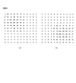
- FIG. 4 is a diagram illustrating an example of a two-dimensional filter matrix.
- FIG. 5 is a diagram illustrating an example of a two-dimensional filter matrix.
- FIG. 6 is a diagram illustrating an example of a two-dimensional filter matrix.
- FIG. 1 is a diagram illustrating a configuration of a digital camera according to an embodiment.
- FIG. 2 is a diagram in which the outer periphery of one microlens of the microlens array is projected onto the photoelectric conversion element array.
- FIG. 3 is a cross-sectional view of
- FIG. 7 is a diagram illustrating a positional relationship between virtual pixels on the focal plane and a projection image projected onto the photoelectric conversion element array via the microlens.
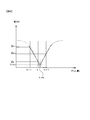
- FIG. 8 is a diagram for explaining the principle of three-point interpolation processing in focus detection calculation.
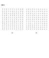
- FIG. 9 is a diagram illustrating an example of a modified two-dimensional filter matrix.
- FIG. 10 is a diagram illustrating a relationship between a microlens of a microlens array in a hexagonal close-packed array and a photoelectric conversion element corresponding to the microlens.
- FIG. 11 is a diagram illustrating an example of a mask matrix for obtaining a photoelectric conversion element output matrix corresponding to a microlens when a hexagonal close-packed microlens array is used.
- FIG. 12 is a diagram for explaining a virtual photoelectric conversion element.
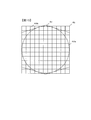
- FIG. 13 is a diagram illustrating the position of a virtual pixel on the focal plane and the center position of the blurred image of the virtual pixel
- FIG. 1 is a diagram showing a configuration of a digital camera according to an embodiment. The configuration of the embodiment will be described with reference to FIG. FIG. 1 shows only devices and units that are directly related to the present invention.
- a photographing lens 3 is attached to a camera body 2.
- the camera body 2 includes an image sensor 4, a drive control device 5, a memory 6, and the like.
- the imaging device 4 includes a microlens array 4a in which minute microlenses 40a are densely arranged on a plane, and a photoelectric conversion element array 4b in which minute photoelectric conversion elements are densely arranged on a plane.
- the microlenses are densely arranged in a two-dimensional square lattice.
- the arrangement of the microlenses is not limited to a square arrangement, and may be a staggered arrangement or a honeycomb arrangement (hexagonal close arrangement).
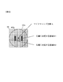
- FIG. 2 is a diagram in which the outer periphery of one microlens 40a of the microlens array 4a is projected onto the photoelectric conversion element array 4b.
- minute photoelectric conversion elements 40b are arranged in a square lattice pattern on the light receiving surface at the focal length of the microlens 40a.
- each microlens 40a of the microlens array 4a includes a plurality of photoelectric conversion elements 40b constituting the photoelectric conversion element array 4b within its outer peripheral range. That is, the light beam that has passed through one microlens is received by the plurality of photoelectric conversion elements 40b.
- the diameter of the microlens 40a is set to the length of 11 photoelectric conversion elements, and a photoelectric conversion element matrix arranged in a square lattice of 11 vertical and 11 horizontal for one microlens is supported. I am letting.
- the number of photoelectric conversion elements 40b corresponding to one microlens 40a is not limited to 11 ⁇ 11 in this embodiment.
- the “right pupil”, “left pupil”, and “microlens optical axis L” described in FIG. 2 will be described later.
- a drive control device 5 includes peripheral components such as a microcomputer (not shown), a memory, an A / D converter, and a drive circuit, and various arithmetic controls, sequence control, lens drive control, and aperture drive control of the camera 1. , And mirror drive control.
- the drive control device 5 includes a pupil data extraction unit 5a, a data string formation unit 5b, a focus calculation unit 5c, an image synthesis unit 5d, a lens drive control unit 5e, and the like that are functionally realized by microcomputer software. ing. Details of these units 5a to 5e will be described later.
- the memory 6 stores various data and images.
- the image memory 6 a stores an image captured by the image sensor 4.
- the optical axis data memory 6b is a memory for storing position data of the optical axis L of each microlens 40a constituting the microlens array 4a.
- the optical axis position data of the optical axis L of the microlens 40a represents the coordinates expressed by the position of the photoelectric conversion element 40b in the photoelectric conversion element array 4b in which the optical axis L of each microlens 40a is located in a decimal order. Is. That is, the position of the optical axis L is accurately represented by a value smaller than a unit in which one photoelectric conversion element 40b is set to 1, for example, 0.5 photoelectric conversion element 40b is 0.5. is there.
- FIG. 2 showing an embodiment, the center of the photoelectric conversion element array 4b having 11 squares and 11 squares in a square lattice arrangement (the position to which X is given in FIG. 2), that is, the photoelectric conversion element array 4b.
- An example is shown in which the center of the photoelectric conversion element 40b at the center is the position of the optical axis L of the microlens 40a.
- the photoelectric conversion element 40b corresponding to each microlens 40a outputs. From the signal, the output of the virtual photoelectric conversion element 400b in which the optical axis L of the microlens 40a passes through the center is obtained by calculation. A matrix of eleven vertical and eleven horizontal squares of virtual photoelectric conversion elements having outputs from these virtual photoelectric conversion elements 400b is created and used for image composition in an embodiment described later. If the virtual photoelectric conversion element output matrix thus obtained is included in the photoelectric conversion element matrix in the following description, the optical axis L of the microlens 40a as shown in FIG. It can be understood in the same way as the centrally located example. Hereinafter, in order to simplify the description, it is assumed that the optical axis L of the microlens 40a is located at the center of the photoelectric conversion element 40b.
- the filter memory 6c is a memory for storing a two-dimensional filter for acting on the photoelectric conversion element matrix when an image is synthesized on a plane perpendicular to the optical axis of the photographing lens 3. This two-dimensional filter will be described later.
- the synthesized image has pixels of the size of the micro lens, and the minimum resolution of the image is the size of the micro lens.
- the synthesized image has pixels smaller than the size of the microlens and having a minimum resolution smaller than that of the microlens.
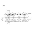
- FIG. 3 is a cross-sectional view of a part of the microlens array 4a and the photoelectric conversion element array 4b cut along a plane including the optical axis of the photographing lens 3.
- the imaging plane of the photographic lens 3 that is, the focal plane S is at a position of a distance y from the plane to which the apex of the microlens 40a included in the microlens array 4a belongs (hereinafter referred to as “microlens apex plane”). Show the case. In this example, the case where the distance y is slightly longer than the focal length f of the microlens 40a included in the microlens array 4a (y> f) is shown.
- the thickness of the microlens 40a is assumed to be almost zero and can be ignored.
- the subject image formed by the taking lens 3 formed on the focal plane S is synthesized based on the output of the photoelectric conversion element array 4b. Note that the subject image formed on the focal plane S has a two-dimensional spread on the focal plane S, but in FIG. 3, a single plane including the optical axis of the photographic lens 3 (hereinafter referred to as “plane shown in FIG. 3”).
- the image composition method of an embodiment will be conceptually described only above.
- the focal length of the photographic lens 3 is approximately equal to the focal length of the microlens 40a.
- each microlens 40a the light beam that passes through each point P1 and is guided to the photoelectric conversion element array 4b via each microlens 40a is the photoelectric conversion element array 4b.
- a blurred image is formed for each microlens 40a.
- the center position of this blurred image is the optical axis position P1 ′ of each micro lens 40a (the position where the optical axis L of the micro lens 40a intersects the light receiving surface of the photoelectric conversion element array 4b), and the photoelectric conversion at the position of the point P1 ′. It has a light quantity distribution centering on the element 40b.
- the photoelectric conversion element array 4b outputs an image signal corresponding to the light amount distribution for each microlens 40a.
- an image of each point P1 formed on the focal plane S is synthesized by an image signal for each microlens 40a.
- a subject image having pixels in units of microlenses 40a around each point P1 on the focal plane S is synthesized.
- a plurality of points on the focal plane S here two points P2 and P3 are arranged at equal intervals and on the optical axis L of each microlens 40a. Place them symmetrically.
- the microlens array 4a and a part of the photoelectric conversion element array 4b are formed by a plane (not shown) obtained by rotating the plane shown in FIG. 3 by 90 degrees about the optical axis of the photographing lens 3.
- a plurality of points, here two points P4 and P5 are arranged on the focal plane S at equal intervals and symmetrically with respect to the optical axis L of each microlens.
- FIG. 13A shows the relationship among points P2, P3, P4, and P5 on the focal plane S.
- FIG. 13A only a part of the focal plane S is shown.
- the outer edge of the microlens 40a located behind the focal plane S is also illustrated.
- a subject image having four pixels is synthesized for each microlens 40a.
- an image having one point P1 as a pixel is synthesized for each microlens 40a, whereas in this embodiment, four points P2 and P3 are made for each microlens 40a. , P4, and P5 are combined as images. Therefore, according to this embodiment, the number of pixels is four times that of a conventional image composition camera, and an image with a resolution four times larger can be synthesized.
- the image composition method in the plane shown in FIG. 3 will be described, but the image composition method in the plane obtained by rotating the plane shown in FIG. 3 about the optical axis of the photographing lens 3 by 90 degrees is also the same.
- the light beam that has passed through the point P2 on the focal plane S and led to the photoelectric conversion element array 4b via each microlens 40a is directed to the position P2 ′ on the photoelectric conversion element array 4b for each microlens 40a. Tying a blurred image. Further, the light beam that has passed through the point P3 on the focal plane S and led to the photoelectric conversion element array 4b through each microlens 40a is blurred at each position of the microlens 40a at the position P3 ′ on the photoelectric conversion element array 4b. Tie.
- These blurred images have a light quantity distribution G with the center positions P2 ′ and P3 ′ as the distribution center, and the photoelectric conversion element array 4b outputs an image signal corresponding to the light quantity distribution G for each microlens 40a. Output.
- the light amount distribution of the blurred image of the points P2 and P3 projected on the photoelectric conversion element array 4b by each microlens 40a shows different point image distributions depending on the curved surface state of the microlens 40a. In order to make it easier to understand, it will be described as a blurred image having a Gaussian light quantity distribution.
- the focal plane S When the focal plane S is between, for example, a position away from the microlens apex plane by the focal length f of the microlens (0 ⁇ y ⁇ f), the focal plane S is smaller than the example shown in FIG. It approaches the lens array 4a. As a result, the angle ⁇ formed by the centers of the light beams exiting the points P2 and P3 becomes gradually larger than the example shown in FIG. Therefore, the blurred images of the points P2 and P3 are diffused beyond the range of the photoelectric conversion element 40b covered by each microlens 40a shown in FIG. 2 to the photoelectric conversion element 40b covered by the adjacent microlens 40a. It becomes difficult to synthesize a blurred image of P3.
- the focal plane S is located on the photographing lens 3 side from the microlens apex surface at a position away from the focal length f of the microlens 40a (y> f)
- the amount of separation (y) increases.
- the angle ⁇ formed by the centers of the light fluxes exiting the points P2 and P3 becomes gradually smaller than the example shown in FIG. Therefore, the blurred images of the points P2 and P3 are reduced and approach on the photoelectric conversion element array 4b, but are within the range of the photoelectric conversion elements 40b covered by the microlenses 40a shown in FIG. 2, and the points P2 and P3 It is possible to synthesize a blurred image.
- the position of the focal plane S has an optimum range that can be combined. Details of this point will be described later.
- the points P2 and P3 are alternately and equally spaced on the focal plane S shown in FIG. 3, so the distance is d / 2. . Therefore, the distance between point P2 or point P3 and point P1 (optical axis L) is both d / 4.
- the center of the light amount distribution of the blurred image on the photoelectric conversion element array 4b at the point P2 or the point P3 The distance x from P2 ′ or the center P3 ′ to the optical axis position P1 ′ of the microlens 40a is both d / 4.
- an image formed at the points P2 and P3 on the focal plane S by the photographing lens 3 is positioned at a position P2 at a distance x from the optical axis position P1 ′ of the microlens 40a on the photoelectric conversion element array 4b by each microlens 40a. It is projected as a blurred image of the light amount distribution G centered on ', P3'.
- the position P2 at a distance x from the optical axis position P1 ′ of each microlens 40a is positioned at a position P2 at a distance x from the optical axis position P1 ′ of each microlens 40a.
- the image data is imaged at points P2 and P3 on the focal plane S at a distance y from the apex surface of the microlens.
- the image data corresponds to the image.
- the distance y from the top surface of the microlens to the focal plane S that is, the possible range of the focal position
- the distance y is smaller than the focal length f of the microlens 40a
- the blurred images at the points P2 and P3 are diffused beyond the range of the photoelectric conversion element 40b covered by each microlens 40a. Becomes impossible.
- the distance y is made larger than the focal length f
- the blurred images at the points P2 and P3 become smaller and overlap on the photoelectric conversion element 40b near the optical axis of each microlens 40a, and the light amount distribution G of the blurred image.
- the image composition method according to the embodiment is effective when the distance y is within a predetermined range from approximately f to 3f with the focal length f of the microlens 40a as a unit.
- the predetermined range (f to 3f) is not necessarily determined uniquely, but is determined according to the specifications such as the diameter and curvature of the microlens 40a, the specifications of the photographing lens 3, and the like.
- the microlens 40a is within the range of the photoelectric conversion element matrix corresponding to each microlens 40a.
- the distance x from the optical axis position P1 ′ to the distribution centers P2 ′ and P3 ′ of the light amount distribution G of the blurred images at the points P2 and P3 is determined by the above equation (1).
- the photographing lens 3 is driven so that the focal plane S falls within the predetermined range (y ⁇ f to 3f). There must be.
- the method of detecting the focus adjustment state of the photographing lens 3 at an arbitrary position in the photographing screen based on the photoelectric conversion element output of the photoelectric conversion element array 4b will be described later in detail.
- the photoelectric conversion element output matrix corresponding to one microlens 40a is subjected to two-dimensional filtering, and an output matrix corresponding to the light quantity distribution G as shown in FIG. 3 is extracted.
- Filter matrix data (hereinafter simply referred to as a filter matrix) used for two-dimensional filter processing is a matrix in which the value of each element decreases along a Gaussian distribution from the center to the periphery as shown in FIG. Thus, a matrix normalized with 256 levels of element values from 0 to 255 is used.
- the filter matrix represents a distribution of weighting factors, and each element of the filter matrix represents a weighting factor.
- the photoelectric conversion element output matrix corresponding to each microlens 40a is composed of eleven vertical elements and eleven horizontal elements
- the two-dimensional filter matrix also includes eleven vertical elements and eleven horizontal elements. Use what you have.
- the matrix of the two-dimensional filter shown in FIG. 4 has the distribution center of the light quantity distribution of the blurred image at the optical axis position P1 ′ of the microlens 40a shown in FIG. 3, and this filter matrix is output to the photoelectric conversion element for each microlens 40a.
- an image of the point P1 on the focal plane S can be synthesized. That is, it is possible to obtain a composite image by the above-described conventional image composition camera.
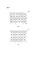
- the two-dimensional shown in FIG. A filter matrix is used in order to generate a composite image in which the point P2 on the focal plane S shown in FIG. 3 (see FIG. 13A) is a virtual pixel. Further, in order to generate a composite image in which a point P3 (see FIG. 13A) on the focal plane S shown in FIG. 3 is a virtual pixel, a two-dimensional filter matrix shown in FIG. 5B is used. On the other hand, in a plane (not shown) obtained by rotating the plane shown in FIG. 3 by 90 degrees about the optical axis of the photographic lens 3, a point P4 (see FIG. 13A) on the focal plane S is a virtual pixel. A two-dimensional filter matrix shown in FIG.
- 3 is a virtual image obtained by using a point P5 on the focal plane S (see FIG. 13A) as a virtual pixel on a plane obtained by rotating the plane shown in FIG. 3 by 90 degrees about the optical axis of the photographing lens 3.
- FIG. 13B shows the relationship between points P1 ', P2', P3 ', P4', and P5 'on the photoelectric conversion element array 4b.
- FIG. 13B only a part of the photoelectric conversion element array 4b is illustrated.
- the outer edge of the microlens 40a included in the microlens array 4a covering the photoelectric conversion element array 4b is also illustrated.
- the two-dimensional filters shown in FIGS. 5A and 5B correspond to positions P2 ′ and P3 ′ that are separated from the optical axis position P1 ′ of the microlens 40a on the photoelectric conversion element array 4b by a distance x in FIG.
- the matrix shown in FIG. 5B is obtained by rotating the matrix shown in FIG. 5A by 180 degrees around the optical axis position P1 'of the micro lens 40a.
- the two-dimensional filter shown in FIGS. 6A and 6B has a photoelectric conversion function in a plane (not shown) obtained by rotating the plane shown in FIG. 3 about 90 degrees around the optical axis of the photographing lens 3.
- Elements corresponding to positions P4 ′ and P5 ′ (both not shown) separated from the optical axis position P1 ′ of the microlens 40a on the element array 4b by a distance x have a maximum value 255, and from the positions P4 ′ and P5 ′.
- This is a matrix filter in which the value of each element decreases along a Gaussian distribution as it moves away from the periphery.
- the matrix shown in FIG. 6B is obtained by rotating the matrix shown in FIG. 6A by 180 degrees around the optical axis position P1 'of the microlens 40a.
- the two-dimensional filter matrix since four virtual pixels are uniformly arranged for each microlens 40a, four contrasting two-dimensional filter matrices are required. That is, in the two-dimensional filter matrix according to the embodiment, one matrix is converted into the optical axis position P1 of the microlens 40a in the order of FIGS. 5A, 6B, 5B, and 6A. It is rotated 90 degrees around '.
- the position where the element of the matrix has the maximum value 255 that is, the position that becomes the distribution center of the blurred image distribution is obtained by the above formula (1) according to the position of the focal plane, that is, the distance y from the apex plane of the microlens to the focal plane. It is done.
- the two-dimensional filter matrix differs depending on the arrangement and number of virtual pixels and the position of the focal plane, and the two-dimensional filter for each arrangement and number of virtual pixels and the position of the focal plane in advance.
- the focus y is assumed to be within a predetermined range (y ⁇ f to 3f)
- the pixel output corresponding to the focus position is obtained, and a high-definition, that is, high-resolution image at the focus position is obtained.
- the image composition unit 5d of the drive control device 5 reads the image data picked up by the image pickup device 4 and stored in the image memory 6a, and creates an output matrix of photoelectric conversion elements corresponding to each microlens.
- the pupil data extraction unit 5a, the data string formation unit 5b, and the focus calculation unit 5c of the drive control device 5 detect the focus adjustment state of the photographing lens 3 at the manually or automatically set focus detection position in the captured image. To do.
- the focus detection position is manually adjusted by moving the cursor to an arbitrary subject position to be focused by operating the operation member while viewing the captured image projected on the monitor (not shown) on the back of the camera. It may be set with. Alternatively, the captured image may be processed to recognize the face portion of a person from the image, and the face portion may be automatically set as a position to be focused.
- the image composition unit 5d Based on the focus detection result at the focus detection position in the image, the image composition unit 5d detects the position y of the focal plane, that is, the distance y from the apex surface of the microlens, and the distance y is a substantially predetermined range with respect to the focal length f of the microlens. It is determined whether or not it is within (y ⁇ f to 3f). If not within the predetermined range, the lens driving control unit 5e of the drive control device 5 adjusts the focus of the photographic lens 3 by controlling the motor of the photographic lens 3 or the like, and the focal plane at the focus detection position is the above-described focal plane. Make sure that it falls within the specified range.
- a filter corresponding to the virtual pixel and the focal plane position is selected from the two-dimensional filters stored in the filter memory 6c. Search for. Then, a two-dimensional filter matrix is applied to the photoelectric conversion element output matrix corresponding to each microlens, the products for each element are integrated, and the integrated value is normalized to a level suitable for the pixel output.
- the image composition unit 5d performs the above processing for each virtual pixel of each microlens, and obtains four virtual pixel outputs for each microlens. Finally, four virtual pixel outputs for each microlens are developed on a two-dimensional plane according to the arrangement of the microlens and the virtual pixel to generate a composite image.
- P4, P4 ′, P5, and P5 ′ are planes obtained by rotating the plane shown in FIG. 3 by 90 degrees about the optical axis of the photographing lens 3, and the microlens array 4a and the photoelectric conversion element array. It is a point in a cross section obtained by cutting a part of 4b (see FIG. 13).
- regions R1 and R2 each consisting of three photoelectric conversion elements 40b that are symmetric with respect to the optical axis position L of the microlens 40a are placed on the exit pupil of the photographing lens 3 by the corresponding microlens 40a. Projected to form a pair of projection areas on the exit pupil. A pair of luminous fluxes passing through the pair of projection areas on the exit pupil of the photographing lens 3 are respectively three photoelectric conversions at symmetrical positions around the optical axis position of the microlens through the photographing lens 3 and the microlens.
- the light is guided to regions R1 and R2 including the element 40b, and images of a pair of pupils (right pupil and left pupil) are formed on the regions R1 and R2, respectively.
- the phase difference between the pair of pupil images that is, the amount of image shift varies depending on the focus adjustment state of the taking lens 3. Therefore, if the image shift amount is calculated based on a pair of image data (a pair of pupil data) corresponding to a pair of pupil images output from each of the three photoelectric conversion elements 40a included in the regions R1 and R2,
- the so-called pupil division phase difference detection method can detect the focus adjustment state of the photographic lens 3, that is, the amount of defocus from the planned focal plane.
- the position and number of photoelectric conversion elements that extract a pair of left and right pupil data are not limited to the position and number of the embodiment shown in FIG. Further, in the above extraction example of a pair of pupil data, an example in which image data is extracted from photoelectric conversion elements at left and right symmetrical positions has been shown. However, depending on the focus detection direction, photoelectric conversion elements at vertical symmetry positions or photoelectric conversion elements at oblique symmetry positions. Image data can be extracted from a conversion element or the like.
- the data string forming unit 5b of the drive control device 5 divides a pair of left and right pupil data corresponding to a predetermined number of microlenses arranged in the left-right direction into right pupil data and left pupil data and arranges them in the order of microlenses.
- a right pupil data string and a left pupil data string are formed.
- the focus calculation unit 5c of the drive control device 5 reads a pair of left and right pupil data strings from the image memory 6a, performs focus detection calculation (correlation calculation) by the above-described pupil division phase difference detection method, and adjusts the focus adjustment state of the photographing lens 3 Is detected.
- the focus detection calculation based on a pair of data strings is well known, but the outline thereof will be described here.
- N 1, 2,..., N
- D (k) ⁇
- the shift amount k that minimizes the difference D (k) is obtained from Equation (2). Since the pair of data strings A and B are discrete numbers, it is not possible to obtain a true shift amount k at which the difference D (k) becomes the minimum value with a resolution equal to or higher than the microlens interval.
- the pair of data strings A and B can be regarded as a combination of sine waves.
- the expression (2) is regarded as the following expression (3).
- D ( ⁇ ) K ⁇
- Equation (4) can also be applied to other spatial frequencies, all of which are independently multiplied by a term related to ⁇ , and it can be seen that the difference equation changes with the absolute value of the sine wave. Further, since the sine wave is linear when ⁇ is near 0, it can be considered that the bottom of the valley sandwiched between straight lines with the same inclination as shown in FIG. 8 is the minimum value.
- a true shift amount k that minimizes the difference D is obtained by the following three-point interpolation calculation.
- the larger difference D is, for example, D (j ⁇ 1).
- the true minimum value Dmin of D (k) is set, and the shift amount k that gives the true minimum difference Dmin is set as the true shift amount kmin .
- the true shift amount kmin is multiplied by a predetermined conversion coefficient m, and the defocus amount DEF from the planned focal plane (microlens apex surface) of the subject image plane by the photographing lens 3, that is, the defocus amount DEF is expressed by the equation (5).
- Ask for. DEF m ⁇ k min (5)
- the distance x to the center positions P2 ′ and P3 ′ and the position of the maximum value of the elements of the two-dimensional filter matrix change.
- a virtual pixel (P2, P3, P4, P5) and a two-dimensional filter corresponding to the position of the focal plane S are stored in advance in the filter memory 6c (see FIG. 1).
- the blur state of the blur image of the virtual pixel changes.
- the focal plane S moves away from the microlens array 4a, that is, the distance y increases, the image of the points P2, P3, P4, and P5 projected onto the photoelectric conversion element array 4b by each microlens 40a becomes less blurred. It approaches the image formation state without any. Therefore, it is necessary to change the position of the maximum value of the element of the two-dimensional filter matrix so as to approach the optical axis position P1 ′ of the microlens, and to reduce the size of the element value set according to the Gaussian distribution. There is.
- the size of the element value distribution according to the Gaussian distribution on the two-dimensional filter matrix is the position of the focal plane where the distance x from the microlens optical axis position P1 ′ to the distribution centers P2 ′ and P3 ′ is considered to be 0, In other words, the distance y from the apex surface of the microlens to the focal plane S is minimized at the position of the focal plane that is considered infinite.
- the diameter D of the blurred image is determined by the diffraction limit, and assuming that the wavelength of light is 540 nm and the F number of the microlens is F / 2.8, the diameter D of the blurred image can be obtained by Expression (6).
- D 2.44 ⁇ ⁇ ⁇ F (6)
- the minimum diameter D is 3.7 ⁇ m, which is about the size of the photoelectric conversion element of the assumed photoelectric conversion element array 4b. It is assumed that there is no blur at the focal position where the distance x from the microlens optical axis position P1 ′ to the distribution centers P2 ′ and P3 ′ is assumed to be 0.
- the matrix of the two-dimensional filter has an element with a value of 255 as the distribution. There is one in the center and all remaining elements can be zero.
- the diameter D of the blurred image when the distance x from the microlens optical axis position P1 ′ to the distribution centers P2 ′ and P3 ′ is 0 is set to 0, and the diameter D of the blurred image is increased as the distance x increases.
- a two-dimensional filter that obtains a more accurate virtual pixel output can be set, and the image quality of the composite image can be improved using such a two-dimensional filter.
- the optically effective shape of the microlens 40a is circular, while the matrix is rectangular (square or rectangular). Therefore, when considering the photoelectric conversion element matrix corresponding to the microlens 40a, the shape between the two is the same. do not do.
- the microlenses 40a are square, the microlens and the photoelectric conversion element matrix can be associated with each other.
- the photoelectric conversion element matrix corresponding to a certain microlens 40a is adjacent.
- the photoelectric conversion element matrix element corresponding to the microlens 40a may be included.
- the range of the photoelectric conversion element 40b corresponding to each microlens 40a is set as a range inscribed in the frame of the hexagon 4c including the microlens 40a as shown in FIG.
- a mask matrix as shown in FIG. 6 is applied to the photoelectric conversion element output matrix.
- the region of the element having a value of 1 indicates the optically effective region of the microlens 40a.
- the digital camera 1 can exhibit the following operational effects.
- the digital camera 1 includes a photographing lens 3, an image sensor 4, and an image composition unit 5d.
- the imaging element 4 includes a microlens array 4a in which a plurality of microlenses 40a are arranged on a plane, and a photoelectric conversion element array 4b in which a plurality of photoelectric conversion elements 40b are arranged on a plane.
- the photoelectric conversion element array 4b receives the light beam from the subject that has passed through the photographing lens 3 through the micro lens array 4a, and outputs an image signal. Based on the image data picked up by the image pickup device 4 in this way, the image composition unit 5 d composes an image on an arbitrary focal plane S of the photographing lens 3.
- a plurality of virtual pixels P2 to P4 are defined for each microlens 40a, and a two-dimensional filter for each of the plurality of virtual pixels P2 to P4 is stored in the filter memory 6c in advance.
- a filter process using a two-dimensional filter is performed on the output matrix of the plurality of photoelectric conversion elements 40b corresponding to each microlens 40a, and the output of each virtual pixel P2 to P4 is calculated to synthesize the image on the focal plane S. I did it. Thereby, it is possible to synthesize a high-definition image with high resolution at an arbitrary focal plane S of the photographing lens 3 based on the data of one captured image.
- the two-dimensional filter has a different matrix element distribution for each focal plane S, and focuses on the distance x between the distribution center position of the element distribution on the matrix and the optical axis position of the microlens 40a on the photoelectric conversion element array 4b. It was made to change according to the surface S. As a result, the projected image on the photoelectric conversion element array 4b of each virtual pixel P2 to P4 on an arbitrary focal plane S can be accurately obtained, and a high-definition image with high resolution can be accurately synthesized.
- the pupil data extraction unit 5a, the data string formation unit 5b, and the focus calculation unit 5c are photographed based on the outputs of a pair of photoelectric conversion elements among the plurality of photoelectric conversion elements 40b corresponding to the respective microlenses 40a.
- a displacement amount of the pair of images by the pair of light beams that have passed through the pupil of the lens 3 is detected.
- the position of the focal plane S of the photographing lens 3 in the image captured by the image sensor 4 is detected.
- the focal plane S can take an arbitrary position.
- the image composition unit 5d composes an image corresponding to the position of the focal plane S thus detected. Therefore, an image corresponding to the focal plane S of the photographing lens 3 that can take an arbitrary position can be synthesized based on the data of one captured image.
- the lens drive control unit 5e adjusts the focus of the photographing lens 3 based on the focus detection results by the pupil data extraction unit 5a, the data string formation unit 5b, and the focus calculation unit 5c.
- a predetermined range for example, a range of f to 3f with respect to the focal length f of the microlens 40a
- the focal plane S falls within the predetermined range. In this way, the focus of the photographic lens 3 is adjusted. Therefore, the image synthesis unit 5d can synthesize a high-resolution image corresponding to the focal plane S of the photographing lens 3 that can take an arbitrary position based on the data of one captured image.
- the matrix of the two-dimensional filter is a matrix having a Gaussian distribution element value centered on the projection position on the photoelectric conversion element array 4b by the microlens 40a of each of the virtual pixels P2 to P4.
- the image composition unit 5d sets the element corresponding to the photoelectric conversion element 40b in the optical effective area of each microlens 40a to 1 and sets the element corresponding to the photoelectric conversion element 40b outside the effective area to 0. It has a matrix mask filter. Prior to the filtering process using the two-dimensional filter, the filtering process using the mask filter is performed on the output matrix of the plurality of photoelectric conversion elements 40b corresponding to each microlens 40a. Therefore, irrespective of the outer diameter shape of the microlens 40a, the photoelectric conversion element 40b in the optically effective area of the microlens 40a can be accurately extracted to obtain a photoelectric conversion element output matrix. The projected image on the photoelectric conversion element array 4b of each of the virtual pixels P2 to P4 can be accurately obtained.
- the filter memory 6c for storing the two-dimensional filter Since the filter memory 6c for storing the two-dimensional filter is provided, it is not necessary to obtain a two-dimensional filter by calculation for each of the focal plane S and the virtual pixels P2 to P4, and the image composition processing can be simplified. .
Landscapes
- Engineering & Computer Science (AREA)
- Multimedia (AREA)
- Signal Processing (AREA)
- Theoretical Computer Science (AREA)
- Physics & Mathematics (AREA)
- General Physics & Mathematics (AREA)
- Computing Systems (AREA)
- Studio Devices (AREA)
- Transforming Light Signals Into Electric Signals (AREA)
- Image Input (AREA)
- Automatic Focus Adjustment (AREA)
Abstract
撮像装置は、撮影光学系と、撮影光学系を透過した光束を受光して信号を出力する複数の光電変換素子を配列した光電変換素子アレイと、撮影光学系と光電変換素子アレイとの間に配置され、かつ複数のマイクロレンズが配列され、複数のマイクロレンズの各々の背後に複数の光電変換素子が光電変換素子アレイに配列されているマイクロレンズアレイと、複数の光電変換素子の出力信号にフィルターマトリクスデータを作用させて、複数のマイクロレンズの各々について撮影光学系による所定の結像面における複数の画素の画素データを作成するデータ作成部と、データ作成部の作成した画素データに基づいて撮影光学系の光軸方向の任意の位置における所定の結像面上の画像を合成する画像合成部とを有し、フィルターマトリクスデータは、複数のマイクロレンズの各々によって光電変換素子アレイ上に形成される複数の画素の各々の投影像の中心位置に対応する要素を分布中心とする所定の強度分布に従った二次元データ配列を有する。
Description
本発明は画像合成を行う撮像装置および画像処理方法に関する。
撮影光学系と、複数のマイクロレンズの各々の背後に複数の光電変換素子を配列した光電変換素子アレイと、その撮影光学系とその光電変換素子アレイとの間に配置され、その複数のマイクロレンズを配列したマイクロレンズアレイとを用いて撮影光学系の光軸方向の任意の位置に焦点の合った画像を合成するようにした画像合成カメラが知られている(特許文献1参照)。
上述した従来の画像合成カメラでは、マイクロレンズアレイと光電変換素子アレイとからなる撮像素子を用いており、撮影光学系によりマイクロレンズアレイの略マイクロレンズ頂点面に被写体像を結像し、各マイクロレンズからの光をそのほぼ焦点位置に配列した光電変換素子上で受光し、デジタル画像データを生成する。その結果、上述した従来の画像合成カメラでは、撮像画像がマイクロレンズの大きさの画素を有することになり、画像の最小分解能はマイクロレンズの大きさになる。
また、上述した従来の画像合成カメラは、撮像画像の奥行き方向の画像合成面の位置、つまり撮影光学系の光軸と垂直に交わる画像合成面の位置は、マイクロレンズアレイ上の各マイクロレンズに対応する光電変換素子の数が多いほど微調整が可能になる。しかし、マイクロレンズを小さくし、かつ光電変換素子アレイ上の各光電変換素子の大きさを縮小してマイクロレンズ1個当たりの光電変換素子数を多くするには限界がある。
本発明の第1の態様によると、撮像装置は、撮影光学系と、撮影光学系を透過した光束を受光して信号を出力する複数の光電変換素子を配列した光電変換素子アレイと、撮影光学系と光電変換素子アレイとの間に配置され、かつ複数のマイクロレンズが配列され、複数のマイクロレンズの各々の背後に複数の光電変換素子が光電変換素子アレイに配列されているマイクロレンズアレイと、複数の光電変換素子の出力信号にフィルターマトリクスデータを作用させて、複数のマイクロレンズの各々について撮影光学系による所定の結像面における複数の画素の画素データを作成するデータ作成部と、データ作成部の作成した画素データに基づいて撮影光学系の光軸方向の任意の位置における所定の結像面上の画像を合成する画像合成部とを有し、フィルターマトリクスデータは、複数のマイクロレンズの各々によって光電変換素子アレイ上に形成される複数の画素の各々の投影像の中心位置に対応する要素を分布中心とする所定の強度分布に従った二次元データ配列を有する。
本発明の第2の態様によると、第1の態様の撮像装置において、中心位置は、所定の結像面の光軸方向の位置に依存し、所定の強度分布は、中心位置に応じて異なるのが好ましい。
本発明の第3の態様によると、第1または第2の態様による撮像装置において、撮影光学系は、被写体像を合焦させる所定の結像面の光軸方向の位置を変化させる焦点調節機能を有しているのが好ましい。
本発明の第4の態様によると、第1または第2の態様による撮像装置において、所定の強度分布は、分布中心における強度が最大となるガウス分布であるのが好ましい。
本発明の第5の態様によると、第3の態様による撮像装置において、撮影光学系は、所定の結像面の光軸方向の位置とマイクロレンズアレイとの距離が、複数のマイクロレンズの各々の焦点距離の略1~3倍の範囲に含まれるように、焦点調節機能により、所定の結像面の光軸方向の位置を変化させるのが好ましい。
本発明の第6の態様によると、第1の態様による撮像装置において、画像合成部は、所定の結像面の位置を変化させる結像位置可変部を有し、データ作成部は、所定の結像面の位置に応じて変化する中心位置に合わせて所定の強度分布を異ならせるのが好ましい。
本発明の第7の態様によると、第6の態様による撮像装置において、結像位置可変部は、所定の結像面の位置とマイクロレンズアレイとの距離が、複数のマイクロレンズの各々の焦点距離の略1~3倍の範囲に含まれるように、所定の結像面の位置を変化させるのが好ましい。
本発明の第8の態様によると、撮影光学系と、撮影光学系を透過した光束を受光して信号を出力する複数の光電変換素子を配列した光電変換素子アレイと、撮影光学系と光電変換素子アレイとの間に配置され、複数のマイクロレンズを配列したマイクロレンズアレイとを有する撮像装置により撮像した画像を処理する画像処理方法は、複数のマイクロレンズの各々によって光電変換素子アレイ上に形成される複数の画素の各々の投影像の中心位置に対応する要素を分布中心とする所定の強度分布に従った二次元データ配列を有するフィルターマトリクスデータを、複数の光電変換素子の出力信号に作用させて、複数のマイクロレンズの各々について撮影光学系による所定の結像面における複数の画素の画素データを作成し、画素データに基づいて撮影光学系の光軸方向の任意の位置における所定の結像面上の画像を合成する。
本発明の第2の態様によると、第1の態様の撮像装置において、中心位置は、所定の結像面の光軸方向の位置に依存し、所定の強度分布は、中心位置に応じて異なるのが好ましい。
本発明の第3の態様によると、第1または第2の態様による撮像装置において、撮影光学系は、被写体像を合焦させる所定の結像面の光軸方向の位置を変化させる焦点調節機能を有しているのが好ましい。
本発明の第4の態様によると、第1または第2の態様による撮像装置において、所定の強度分布は、分布中心における強度が最大となるガウス分布であるのが好ましい。
本発明の第5の態様によると、第3の態様による撮像装置において、撮影光学系は、所定の結像面の光軸方向の位置とマイクロレンズアレイとの距離が、複数のマイクロレンズの各々の焦点距離の略1~3倍の範囲に含まれるように、焦点調節機能により、所定の結像面の光軸方向の位置を変化させるのが好ましい。
本発明の第6の態様によると、第1の態様による撮像装置において、画像合成部は、所定の結像面の位置を変化させる結像位置可変部を有し、データ作成部は、所定の結像面の位置に応じて変化する中心位置に合わせて所定の強度分布を異ならせるのが好ましい。
本発明の第7の態様によると、第6の態様による撮像装置において、結像位置可変部は、所定の結像面の位置とマイクロレンズアレイとの距離が、複数のマイクロレンズの各々の焦点距離の略1~3倍の範囲に含まれるように、所定の結像面の位置を変化させるのが好ましい。
本発明の第8の態様によると、撮影光学系と、撮影光学系を透過した光束を受光して信号を出力する複数の光電変換素子を配列した光電変換素子アレイと、撮影光学系と光電変換素子アレイとの間に配置され、複数のマイクロレンズを配列したマイクロレンズアレイとを有する撮像装置により撮像した画像を処理する画像処理方法は、複数のマイクロレンズの各々によって光電変換素子アレイ上に形成される複数の画素の各々の投影像の中心位置に対応する要素を分布中心とする所定の強度分布に従った二次元データ配列を有するフィルターマトリクスデータを、複数の光電変換素子の出力信号に作用させて、複数のマイクロレンズの各々について撮影光学系による所定の結像面における複数の画素の画素データを作成し、画素データに基づいて撮影光学系の光軸方向の任意の位置における所定の結像面上の画像を合成する。
本発明の撮像装置をデジタルカメラに適用した一実施の形態を説明する。図1は一実施の形態のデジタルカメラの構成を示す図であり、この図により一実施の形態の構成を説明する。なお、図1では本発明に直接関係のある装置およびユニットのみを図示する。
一実施の形態のデジタルカメラ1には、カメラボディ2に撮影レンズ3が装着されている。カメラボディ2は撮像素子4、駆動制御装置5、メモリ6などを備えている。撮像素子4は、微小なマイクロレンズ40aを平面上に稠密に配列したマイクロレンズアレイ4aと、微小な光電変換素子を平面上に稠密に配列した光電変換素子アレイ4bとから構成される。
一実施の形態のマイクロレンズアレイ4aでは、マイクロレンズが二次元状に稠密に正方格子配列されている。なお、マイクロレンズの配列は正方配列に限定されず、千鳥状配列やハニカム状配列(六方稠密配列)としてもよい。
図2は、マイクロレンズアレイ4aの一つのマイクロレンズ40aの外周を光電変換素子アレイ4b上に投影した図である。一実施の形態の光電変換素子アレイ4bでは、微小な光電変換素子40bがマイクロレンズ40aの焦点距離の位置にある受光面に正方格子状に配列されている。マイクロレンズアレイ4aの各マイクロレンズ40aは、図2に示すように光電変換素子アレイ4bを構成する複数の光電変換素子40bをその外周範囲内に包含している。すなわち、一つのマイクロレンズを通った光束は複数の光電変換素子40bで受光される。
この一実施の形態では、マイクロレンズ40aの直径を光電変換素子11個分の長さとし、マイクロレンズ1個に対し縦11個、横11個の正方格子状に配列された光電変換素子マトリクスを対応させている。なお、1個のマイクロレンズ40aに対応する光電変換素子40bの個数はこの一実施の形態の11×11個に限定されない。また、図2の中に記載した“右瞳”、“左瞳”および“マイクロレンズ光軸L”については後述する。
図1において、駆動制御装置5は、図示しないマイクロコンピューターとメモリ、A/Dコンバーター、および駆動回路などの周辺部品を含み、カメラ1の種々の演算制御、シーケンス制御、レンズ駆動制御、絞り駆動制御、およびミラー駆動制御などを実行する。駆動制御装置5は、マイクロコンピューターのソフトウエアにより機能的に実現された瞳データ抽出部5a、データ列形成部5b、焦点演算部5c、画像合成部5d、およびレンズ駆動制御部5eなどを有している。これらの各部5a~5eの詳細については後述する。
メモリ6は種々のデータや画像を記憶する。画像メモリ6aは撮像素子4により撮像された画像を記憶する。光軸データメモリ6bは、図2に示すように、マイクロレンズアレイ4aを構成する各マイクロレンズ40aの光軸Lの位置データを記憶するメモリである。このマイクロレンズ40aの光軸Lの光軸位置データは、各マイクロレンズ40aの光軸Lが位置する光電変換素子アレイ4bにおける光電変換素子40bの位置で表される座標を小数のオーダで表したものである。つまり、1個の光電変換素子40bを1とした単位よりも小さい値、例えば0.5個の光電変換素子40bを0.5というようにして、光軸Lの位置を正確に表したものである。
なお、一実施の形態を示す図2では、縦11個、横11個の正方格子配列の光電変換素子アレイ4bの中心(図2において、×印を付与した位置)、すなわち光電変換素子アレイ4bの中央にある光電変換素子40bの中心を、マイクロレンズ40aの光軸Lの位置とする例を示す。しかし、実際にはマイクロレンズ40aの光軸Lが光電変換素子40bの中心に位置するようにマイクロレンズアレイ4aと光電変換素子アレイ4bを製作することは難しい。
そこで、図12に示すように、光軸データメモリ6bに記憶されている各マイクロレンズ40aの光軸Lの光軸位置データに基づいて、各マイクロレンズ40aに対応する光電変換素子40bの出力する信号から、マイクロレンズ40aの光軸Lが中心を通る仮想的な光電変換素子400bの出力を演算により求める。これらの仮想的な光電変換素子400bの出力を有する縦11個、横11個の正方格子配列の仮想的な光電変換素子出力のマトリクスを作成し、後述する一実施の形態の画像合成に用いる。なお、こうして求めた仮想的な光電変換素子出力のマトリクスを以下の説明における光電変換素子マトリクスに含まれるものとすれば、図2に示すようなマイクロレンズ40aの光軸Lが光電変換素子40bの中心に位置する例と同様に理解することができる。以下においては、説明を簡単にするため、マイクロレンズ40aの光軸Lは光電変換素子40bの中心に位置するものとする。
フィルターメモリ6cは、撮影レンズ3の光軸に対して垂直な面において画像を合成する際に、光電変換素子マトリクスに作用させるための二次元フィルターを記憶するメモリである。この二次元フィルターについては後述する。
次に、高分解能な画像を合成する原理について説明する。上述したように、従来の画像合成カメラでは、合成された画像がマイクロレンズの大きさの画素を有し、画像の最小分解能はマイクロレンズの大きさになっていた。この一実施の形態では、マイクロレンズの大きさよりも小さい画素を有し、最小分解能がマイクロレンズよりも小さい高精細な画像を合成する。
図3は、マイクロレンズアレイ4aと光電変換素子アレイ4bの一部分を、撮影レンズ3の光軸を含む平面で切った断面図である。図3において、撮影レンズ3の結像面、すなわち焦点面Sがマイクロレンズアレイ4aに含まれるマイクロレンズ40aの頂点の属する平面(以下、「マイクロレンズ頂点面」という)から距離yの位置にある場合を示す。この例では、距離yがマイクロレンズアレイ4aに含まれるマイクロレンズ40aの焦点距離fよりわずかに長い距離(y>f)とした場合を示す。マイクロレンズ40aは極めて薄いため、以下の説明においては、マイクロレンズ40aの厚さはほぼ0として無視できるものとして説明する。この一実施の形態では、焦点面Sに結像された撮影レンズ3による被写体像を、光電変換素子アレイ4bの出力に基づいて合成する。なお、焦点面Sに結像された被写体像は、焦点面Sにおいて二次元的な広がりを有するが、図3では撮影レンズ3の光軸を含む一つの平面(以下、「図3に示す平面」という)上においてのみ、一実施の形態の画像合成法を概念的に説明する。撮影レンズ3の焦点距離は、マイクロレンズ40aの焦点距離と略等しいものとする。
焦点面Sと各マイクロレンズの光軸Lとが交わる点をP1とすると、各点P1を通り、各マイクロレンズ40aを介して光電変換素子アレイ4bへ導かれた光束は、光電変換素子アレイ4b上において各マイクロレンズ40aごとにボケ像を結像する。このボケ像の中心位置は各マイクロレンズ40aの光軸位置P1’(マイクロレンズ40aの光軸Lが光電変換素子アレイ4bの受光面と交わる位置)であり、点P1’の位置にある光電変換素子40bを分布中心とした光量分布を有する。光電変換素子アレイ4bは各マイクロレンズ40aごとに光量分布に応じた画像信号を出力する。上述した従来の画像合成カメラでは、各マイクロレンズ40aごとの画像信号により焦点面S上に結像された各点P1の像を合成する。これにより、焦点面S上の各点P1を中心としたマイクロレンズ40a単位の画素を有する被写体像が合成される。
これに対しこの一実施の形態では、図3に示すように焦点面S上に複数の点、ここでは2個の点P2、P3を等間隔に、かつ、各マイクロレンズ40aの光軸Lに対して対称な位置に配置する。また、この一実施の形態では、図3に示す平面を撮影レンズ3の光軸を中心にして90度回転させた平面(不図示)で、マイクロレンズアレイ4aと光電変換素子アレイ4bの一部分を切った断面において、焦点面S上に複数の点、ここでは2個の点P4、P5を等間隔に、かつ、各マイクロレンズの光軸Lに対して対称な位置に配置する。図13(a)に焦点面S上における点P2、P3、P4、P5の関係を示す。図13(a)において、焦点面Sはその一部分のみを図示している。説明の便宜上、焦点面Sの背後に位置するマイクロレンズ40aの外縁をも図示している。これらの点P2、P3、P4、P5を仮想的な画素とし、マイクロレンズ40aごとに4個の画素を有する被写体像を合成する。
上述した従来の画像合成カメラでは、マイクロレンズ40aごとに1個の点P1を画素とする画像を合成するのに対し、この一実施の形態では、マイクロレンズ40aごとに4個の点P2、P3、P4、P5を仮想的な画素とする画像を合成する。したがって、この一実施の形態によれば、従来の画像合成カメラに比べ画素数が4倍になり、4倍の分解能の画像を合成することができる。なお、以下では、図3に示す平面における画像合成法を説明するが、図3に示す平面を撮影レンズ3の光軸を中心にして90度回転した平面における画像合成法も同様である。
図3において、焦点面S上の点P2を通り、各マイクロレンズ40aを介して光電変換素子アレイ4bへ導かれた光束は、光電変換素子アレイ4b上の位置P2’に各マイクロレンズ40aごとにボケ像を結ぶ。また、焦点面S上の点P3を通り、各マイクロレンズ40aを介して光電変換素子アレイ4bへ導かれた光束は、光電変換素子アレイ4b上の位置P3’に各マイクロレンズ40aごとにボケ像を結ぶ。これらのボケ像は、それらの中心位置P2’、P3’を分布中心とした光量分布Gを有し、光電変換素子アレイ4bは各マイクロレンズ40aごとにこれらの光量分布Gに応じた画像信号を出力する。
各マイクロレンズ40aにより光電変換素子アレイ4b上に投影される点P2、P3のボケ像の光量分布は、マイクロレンズ40aの曲面の状態により異なる点像分布を示すが、この一実施の形態では説明を解りやすくするためにガウス分布の光量分布を有するボケ像とみなして説明する。
焦点面Sが、例えばマイクロレンズ頂点面からマイクロレンズの焦点距離fだけ離れた位置までの間にある場合には(0<y<f)、焦点面Sが図3に示した例よりもマイクロレンズアレイ4aに近づいてくる。その結果、点P2、P3を出た光束の中心のなす角度αが図3に示した例よりも徐々に大きくなる。したがって、点P2、P3のボケ像は図2に示す各マイクロレンズ40aが覆う光電変換素子40bの範囲を超えて、隣接するマイクロレンズ40aが覆う光電変換素子40bにまで拡散するため、点P2、P3のボケ像を合成することが困難になる。
一方、焦点面Sが、マイクロレンズ頂点面から撮影レンズ3側に、マイクロレンズ40aの焦点距離fよりも離れた位置にある場合には(y>f)、離れる量(y)が大きくなるにつれ、点P2、P3を出た光束の中心のなす角度αは図3に示した例よりも徐々に小さくなる。したがって、点P2、P3のボケ像は縮小し、光電変換素子アレイ4b上で近づいてくるが、図2に示す各マイクロレンズ40aが覆う光電変換素子40bの範囲に収まっていて、点P2、P3のボケ像を合成することが可能である。離れる量(y)がさらに大きくなると、点P2、P3のボケ像は光電変換素子アレイ4b上で近づきすぎ、両者を分離できなくなる。したがって、焦点面Sの位置には合成できる最適な範囲がある。この点については詳細を後述する。
マイクロレンズ40aの配列ピッチをdとすると、上述したように、点P2および点P3は、図3に示す焦点面S上において交互にかつ等間隔に位置するので、その間隔はd/2となる。したがって、点P2または点P3と点P1(光軸L)との距離は、ともにd/4である。マイクロレンズ頂点面から焦点面Sまでの距離yが、マイクロレンズ40aの焦点距離fと等しい(y=f)場合、点P2または点P3の光電変換素子アレイ4b上のボケ像の光量分布の中心P2’または中心P3’からマイクロレンズ40aの光軸位置P1’までの距離xは、ともにd/4となる。マイクロレンズ頂点面から焦点面Sまでの距離yが変化する場合、点P2、P3の光電変換素子アレイ4b上のボケ像の光量分布の中心P2’またはP3’からマイクロレンズ40aの光軸位置P1’までの距離xは、上述したようにマイクロレンズ40aの厚さを0とみなすと、式(1)で表される。
x=d・f/(4・y) (1)
x=d・f/(4・y) (1)
つまり、撮影レンズ3により焦点面S上の点P2、P3に結像された像は、各マイクロレンズ40aによって光電変換素子アレイ4b上のマイクロレンズ40aの光軸位置P1’から距離xの位置P2’、P3’を中心とする光量分布Gのボケ像として投影される。換言すれば、撮像素子4により撮像された被写体像の画像データの内の、各マイクロレンズ40aに対応する光電変換素子出力マトリクスから、各マイクロレンズ40aの光軸位置P1’から距離xの位置P2’,P3’を分布中心とするガウス分布に相当する画像データを抽出すれば、その画像データはマイクロレンズ頂点面から距離yの位置にある焦点面S上の点P2、P3に結像された像に対応する画像データとなる。
ここで、マイクロレンズ頂点面から焦点面Sまでの距離y、すなわち焦点位置の取り得る範囲について考察する。上述したように、距離yがマイクロレンズ40aの焦点距離fより小さい場合には、点P2、P3のボケ像が各マイクロレンズ40aが覆う光電変換素子40bの範囲を超えて拡散するため、画像合成が不可能になる。逆に、距離yを焦点距離fより大きくしていくと、点P2、P3のボケ像が小さくなって各マイクロレンズ40aの光軸付近の光電変換素子40b上に重なり、ボケ像の光量分布Gが光軸付近に集中して光電変換素子40b単位での分離と解析が困難になる。したがって、一実施の形態による画像合成法は、距離yがマイクロレンズ40aの焦点距離fを単位とする略fから3fまでの所定範囲内にある場合に有効である。
なお、この所定範囲(f~3f)は必ずしも一義的に決定されるものではなく、マイクロレンズ40aの径や曲率などの仕様、撮影レンズ3の仕様などに応じて決定されるものである。
マイクロレンズ頂点面から焦点面Sまでの距離yが略上記所定範囲(y≒f~3f)内にある場合には、各マイクロレンズ40aに対応する光電変換素子マトリクスの範囲内において、マイクロレンズ40aの光軸位置P1’から点P2、P3のボケ像の光量分布Gの分布中心P2’、P3’までの距離xを上記式(1)により決定する。そして、各マイクロレンズ40aに対応する光電変換素子出力マトリクスから位置P2’,P3’を中心とするガウス分布に相当する画像データを抽出すれば、焦点面S上の点P2、P3の像を合成することができる。
しかし、焦点面Sの位置が上記所定範囲(y≒f~3f)を超える場合には、撮影レンズ3を駆動して焦点面Sが上記所定範囲(y≒f~3f)内に入るようにしなければならない。なお、光電変換素子アレイ4bの光電変換素子出力に基づいて撮影画面内の任意の位置の撮影レンズ3の焦点調節状態を検出する方法については、詳細を後述する。
次に、図1に示す画像合成部5dによる画像合成の具体的な方法について説明する。ここでは、ある一つのマイクロレンズ40aとそのマイクロレンズ40aに対応する光電変換素子マトリクスに対する画像合成処理を説明するが、他のマイクロレンズ40aと対応する光電変換素子マトリクスに対する処理も同様である。
この一実施の形態では、一つのマイクロレンズ40aに対応する光電変換素子出力マトリクスに対して二次元フィルター処理を施し、図3に示すような光量分布Gに相当する出力マトリクスを抽出する。二次元フィルター処理に用いられるフィルターマトリクスデータ(以下、単にフィルターマトリクスという)は、例えば図4に示すように、中心から周辺に向かって各要素の値がガウス分布に沿って斬減するマトリクスであって、要素の値が0~255の256段階に正規化されたマトリクスを用いる。換言すると、フィルターマトリクスは重み係数の分布を表しており、フィルターマトリクスの各要素は重み係数を表している。上述したように、各マイクロレンズ40aに対応する光電変換素子出力マトリクスは縦11個、横11個の要素から構成されているので、二次元フィルターのマトリクスも縦11個、横11個の要素を有するものを用いる。
このような二次元フィルターのマトリクスを、一つのマイクロレンズ40aに対応する光電変換素子出力マトリクスに作用させ、要素ごとに積算した後、画素の出力レベルに正規化すれば、焦点面S上の対応する点、すなわち仮想的な画素の像を合成することができる。
例えば図4に示す二次元フィルターのマトリクスは、図3に示すマイクロレンズ40aの光軸位置P1’にボケ像の光量分布の分布中心があり、このフィルターマトリクスをマイクロレンズ40aごとの光電変換素子出力マトリクスに作用させると、焦点面S上の点P1の像を合成することができる。つまり、上述した従来の画像合成カメラによる合成画像を得ることができる。
この一実施の形態では、図3に示す焦点面S上の点P2(図13(a)参照)を仮想的な画素とする合成画像を生成するために、図5(a)に示す二次元フィルターマトリクスを用いる。また、図3に示す焦点面S上の点P3(図13(a)参照)を仮想的な画素とする合成画像を生成するために、図5(b)に示す二次元フィルターマトリクスを用いる。一方、図3に示す平面を撮影レンズ3の光軸を中心にして90度回転した平面(不図示)において、焦点面S上の点P4(図13(a)参照)を仮想的な画素とする合成画像を生成するために、図6(a)に示す二次元フィルターマトリクスを用いる。また、図3に示す平面を撮影レンズ3の光軸を中心にして90度回転した平面において、焦点面S上の点P5(図13(a)参照)を仮想的な画素とする合成画像を生成するために、図6(b)に示す二次元フィルターマトリクスを用いる。
図13(b)に光電変換素子アレイ4b上における点P1’、P2’、P3’、P4’、P5’の関係を示す。図13(b)において、光電変換素子アレイ4bはその一部分のみを図示している。説明の便宜上、光電変換素子アレイ4bを覆うマイクロレンズアレイ4aに含まれるマイクロレンズ40aの外縁をも図示している。図5(a)、(b)に示す二次元フィルターは、図3において光電変換素子アレイ4b上のマイクロレンズ40aの光軸位置P1’から距離xだけ離れた位置P2’、P3’に対応する要素が最大値255を有し、位置P2’、P3’から周辺に遠ざかるにしたがって各要素の値がガウス分布に沿って斬減するマトリクスのフィルターである(図13(b)参照)。図5(b)に示すマトリクスは、マイクロレンズ40aの光軸位置P1’を中心に図5(a)に示すマトリクスを180度回転させたものである。
同様に、図6(a)、(b)に示す二次元フィルターは、図3に示す平面を撮影レンズ3の光軸を中心にして90度回転させた平面(不図示)おいて、光電変換素子アレイ4b上のマイクロレンズ40aの光軸位置P1’から距離xだけ離れた位置P4’、P5’(ともに不図示)に対応する要素が最大値255を有し、位置P4’、P5’から周辺に遠ざかるにしたがって各要素の値がガウス分布に沿って斬減するマトリクスのフィルターである。図6(b)に示すマトリクスは、マイクロレンズ40aの光軸位置P1’を中心に図6(a)に示すマトリクスを180度回転させたものである。
この一実施の形態では、各マイクロレンズ40aに対して4個の仮想的な画素を均等に配置しているので、互いに対照的な4個の二次元フィルターマトリクスが必要になる。つまり、一実施の形態の二次元フィルターマトリクスは、1つのマトリクスを図5(a)、図6(b)、図5(b)、図6(a)の順にマイクロレンズ40aの光軸位置P1’を中心にして90度ずつ回転させたものである。マトリクスの要素が最大値255になる位置、つまりボケ像分布の分布中心になる位置は、焦点面の位置、すなわちマイクロレンズ頂点面から焦点面までの距離yに応じて上記式(1)により求められる。
換言すれば、仮想的な画素の配置と個数、および焦点面の位置ごとに二次元フィルターマトリクスが異なることになり、予め仮想的な画素の配置と個数、および焦点面の位置ごとの二次元フィルターをフィルターメモリ6c(図1参照)に記憶させておく必要がある。これにより、上述した距離yが略所定範囲(y≒f~3f)内において、焦点の位置を想定するとそれに応じた画素出力が得られ、その焦点位置における高精細な、つまり高分解能な画像を合成することができる。
なお、この一実施の形態では、各マイクロレンズ40aに対して任意の焦点面S上に4個の仮想的な画素を均等に配置する例を示すが、仮想画素の個数と配置はこの一実施の形態に限定されるものではない。
図1において、駆動制御装置5の画像合成部5dは、撮像素子4により撮像され画像メモリ6aに記憶された画像データを読み出し、各マイクロレンズごとに対応する光電変換素子の出力マトリクスを作成する。一方、駆動制御装置5の瞳データ抽出部5a、データ列形成部5bおよび焦点演算部5cは、撮像画像の中の手動または自動で設定された焦点検出位置における撮影レンズ3の焦点調節状態を検出する。
なお、この焦点検出位置はカメラ背面のモニター(不図示)に写し出された上記撮像画像を見ながら、撮影者が操作部材を操作してピントを合わせたい任意の被写体位置にカーソルを移動して手動で設定してもよい。あるいは、撮像画像を処理して画像内から人物の顔の部分を認識し、顔の部分をピントを合わせたい位置として自動で設定するものであってもよい。
画像合成部5dは、画像内の焦点検出位置における焦点検出結果に基づいて、焦点面の位置すなわちマイクロレンズ頂点面からの距離yを検出し、距離yがマイクロレンズの焦点距離fに関して略所定範囲(y≒f~3f)内にあるか否かを判別する。当該所定範囲内にない場合には、駆動制御装置5のレンズ駆動制御部5eにより撮影レンズ3のモータを駆動させる等の制御により撮影レンズ3の焦点調節を行い、焦点検出位置の焦点面が上記所定範囲内に入るようにする。
設定された焦点検出位置の焦点面の位置が上記所定範囲内にある場合には、フィルターメモリ6cに記憶されている二次元フィルターの中から、仮想的な画素と焦点面の位置に対応するフィルターを検索する。そして、各マイクロレンズごとに対応する光電変換素子出力マトリクスに対して二次元フィルターマトリクスを作用させ、要素ごとの積を積算した後、積算値を画素出力にふさわしいレベルに正規化する。
画像合成部5dは、以上の処理を各マイクロレンズの仮想画素ごとに行い、マイクロレンズごとに4個の仮想画素出力を得る。最後に、これらのマイクロレンズごとの4個の仮想画素出力をマイクロレンズと仮想画素の配置にしたがって二次元平面上に展開し、合成画像を生成する。
マイクロレンズごとの4個の仮想画素出力を平面上に展開して合成画像を生成する際には、次のような仮想画素出力の整列処理を行う。図3に示すように、焦点面S上の点P2、P3と、マイクロレンズアレイ4b上の位置P2’、P3’に投影されるボケ像とは、マイクロレンズごとに位置関係が反転している。そのため、図7(a)に示す光電変換素子アレイ4b上の位置P2’、P3’,P4’,P5’のボケ像の配列を、図7(b)に示すように焦点面S上の点P2、P3、P4、P5の配列に合わせて整列させる。なお、図7において、P4、P4’、P5、P5’は、図3に示す平面を撮影レンズ3の光軸を中心にして90度回転させた平面で、マイクロレンズアレイ4aと光電変換素子アレイ4bの一部分を切った断面における点である(図13参照)。
次に、図1に示す瞳データ抽出部5a、データ列形成部5bおよび焦点演算部5cによる焦点検出方法を説明する。図2において、マイクロレンズ40aの光軸位置Lに対して左右対称位置にあるそれぞれ3個の光電変換素子40bからなる領域R1、R2は、対応するマイクロレンズ40aにより撮影レンズ3の射出瞳上に投影され、射出瞳上に一対の投影領域を形成する。撮影レンズ3の射出瞳上のこの一対の投影領域を通過する一対の光束は、撮影レンズ3およびマイクロレンズを介してマイクロレンズ光軸位置を中心とする左右対称位置にあるそれぞれ3個の光電変換素子40bからなる領域R1、R2へ導かれ、それぞれ領域R1、R2上に一対の瞳(右瞳および左瞳)の像が結像される。
この一対の瞳の像の位相差、すなわち像ずれ量は撮影レンズ3の焦点調節状態に応じて変化する。そのため、領域R1、R2に含まれるそれぞれ3個の光電変換素子40aから出力される一対の瞳の像に対応する一対の画像データ(一対の瞳データ)に基づいて像ずれ量を演算すれば、いわゆる瞳分割位相差検出方式により撮影レンズ3の焦点調節状態、つまり予定焦点面からの焦点の外れ量を検出することができる。
なお、左右一対の瞳データを抽出する光電変換素子の位置および個数は、図2に示す一実施の形態の位置および個数に限定されない。また、一対の瞳データの上記抽出例では左右対称位置の光電変換素子から画像データを抽出する例を示したが、焦点検出方向に応じて上下対称位置の光電変換素子、あるいは斜め対称位置の光電変換素子などから画像データを抽出することができる。
駆動制御装置5のデータ列形成部5bは、左右方向に配列されている所定数のマイクロレンズに対応する左右一対の瞳データを、右瞳データと左瞳データに分けてマイクロレンズの順に並べ、右瞳データ列と左瞳データ列を構成する。
駆動制御装置5の焦点演算部5cは、画像メモリ6aから左右一対の瞳データ列を読み出し、上述した瞳分割位相差検出方式により焦点検出演算(相関演算)を行い、撮影レンズ3の焦点調節状態を検出する。
一対のデータ列に基づく焦点検出演算については周知であるが、ここでその概要を説明する。上述した左右一対の瞳データ列をA{ai}、B{bi}とし、データの個数をそれぞれN個(i=1,2,・・・,N)とする。一対のデータ列A、Bのずらし量をkとしたとき、データ列AとBの差分D(k)は式(2)で表される。
D(k)=Σ|ai+k-bi| (2)
D(k)=Σ|ai+k-bi| (2)
式(2)により差分D(k)が最も小さくなるずらし量kを求める。一対のデータ列A、Bは離散的な数列であるから、マイクロレンズの間隔以上の分解能で差分D(k)が最小値となる真のずらし量kを得ることはできない。
ここで、一対のデータ列A、Bを正弦波の合成とみなすことができ、その内のある空間周波数ωを持つ正弦波信号に注目すると、式(2)は次式(3)とみなすことができる。
D(θ)=K∫|sin(ωx+θ)-sinωx|dx (3)
D(θ)=K∫|sin(ωx+θ)-sinωx|dx (3)
さらに式(3)を変形すると次式が得られる。
D(θ)=K’|sin(θ/2)・sin(ωx+φ)| (4)
D(θ)=K’|sin(θ/2)・sin(ωx+φ)| (4)
式(4)は他の空間周波数にも適用でき、これらもすべてθに関する項が独立に乗ぜられていることから、差分式は正弦波の絶対値で変化することがわかる。また、θが0付近では正弦波は線形であるから、図8に示すように左右同じ傾きの直線に挟まれた、谷間の底が最小値であると見なせる。
以下の三点内挿演算により差分Dが最小となる真のずらし量kを求める。まず、式(2)により差分D(k)の最小値D(j)とその時のずらし量k=jを求める。次に、最小値D(j)を与えるずらし量k=jに隣接するずらし量k=(j-1)とk=(j+1)とに対する差分D(j-1)、D(j+1)の内、差分Dが大きい方が、たとえばD(j-1)であるとする。この場合において、二点(k,D(k))=(j,D(j)),(j-1,D(j-1))を結ぶ直線を引き、この直線の傾きをaとする。二番目に小さい差分D(j+1)を与えるずらし量k=(j+1)に対応する点(j+1,D(j+1))を通る傾き(-a)の直線を引き、2本の直線の交点を差分D(k)の真の最小値Dminとし、その真の最小差分Dminを与えるずらし量kを真のずらし量kminとする。
この真のずらし量kminに所定の変換係数mを乗じ、撮影レンズ3による被写体像面の予定焦点面(マイクロレンズ頂点面)からの焦点の外れ量、すなわちデフォーカス量DEFを式(5)により求める。
DEF=m・kmin (5)
DEF=m・kmin (5)
以上の方法により、撮像画像の中の手動または自動で設定された焦点検出位置における撮影レンズ3の焦点調節状態を検出することができる。
次に、仮想的な画素に対するボケ像について説明する。図3に示すように、焦点面Sの位置、すなわちマイクロレンズ頂点面から焦点面Sまでの距離yに応じて、光電変換素子アレイ4b上のマイクロレンズ光軸位置P1’から仮想画素のボケ像の中心位置P2’、P3’までの距離xと、二次元フィルターマトリクスの要素の最大値の位置とが変化する。この一実施の形態では、仮想的な画素(P2、P3、P4、P5)と焦点面Sの位置に応じた二次元フィルターをフィルターメモリ6c(図1参照)に予め記憶しておく例を示したが、仮想的な画素と焦点面の位置に応じてその都度演算により求めてもよい。
ところで、焦点面Sの位置が移動すると、仮想画素のボケ像のボケ状態が変化する。焦点面Sがマイクロレンズアレイ4aから遠ざかる、つまり距離yが大きくなるほど、各マイクロレンズ40aにより光電変換素子アレイ4b上に投影される点P2、P3、P4、P5の像はボケが小さくなってボケの無い結像状態に近づいていく。したがって、二次元フィルターマトリクスの要素の最大値の位置をマイクロレンズの光軸位置P1’に近づくように変えると同時に、ガウス分布に応じて設定された要素の値の分布の大きさを小さくする必要がある。二次元フィルターマトリクス上のガウス分布に応じた要素の値の分布の大きさは、マイクロレンズ光軸位置P1’から分布中心P2’、P3’までの距離xが0とみなされる焦点面の位置、すなわちマイクロレンズ頂点面から焦点面Sまでの距離yが無限とみなされる焦点面の位置において最小になる。
ボケ像の径Dは回折限界で決まると考え、光の波長を540nm、マイクロレンズのFナンバーをF/2.8とすると、ボケ像の径Dは、式(6)により求められる。
D=2.44・λ・F (6)
D=2.44・λ・F (6)
式(6)によると、最小の径Dは3.7μmとなり、想定している光電変換素子アレイ4bの光電変換素子程度の大きさになる。マイクロレンズ光軸位置P1’から分布中心P2’、P3’までの距離xが0とみなされる焦点位置においてボケがなくなるとし、このときの二次元フィルターのマトリクスは、値が255の要素が分布の中心に一つあって残りの要素はすべて0とすることができる。つまり、マイクロレンズ光軸位置P1’から分布中心P2’、P3’までの距離xが0のときのボケ像の径Dを0とし、距離xが大きくなるにしたがってボケ像の径Dを大きくすれば、より正確な仮想画素出力を得る二次元フィルターを設定することができ、このような二次元フィルターを用いて合成画像の画質を向上させることができる。
なお、マイクロレンズ光軸位置P1’から分布中心P2’、P3’までの距離xが変化してもボケ像の径Dを変えずに一定とするか、あるいは、さらに簡略化してボケがないものとしても、ある程度の画質の合成画像を得ることができる。つまり、図3において点P2、P3がマイクロレンズ40aにより投射される位置P2’、P3’の光電変換素子出力のみを点P2、P3に対応する仮想画素出力としてもよい。この場合、図9(a)、(b)に示すようなマトリクス、つまり点P2、P3がマイクロレンズ40aにより投射される位置P2’、P3’に対応する要素のみ0以外の値を持ち、他の要素の値をすべて0としたマトリクスの二次元フィルターとする。
次に、マイクロレンズ40aの外径形状とマトリクスとの整合について説明する。マイクロレンズ40aの光学的に有効な形状は円形であり、一方、マトリクスは矩形(正方形または長方形)であるから、マイクロレンズ40aに対応する光電変換素子マトリクスを考える場合に両者の間の形状は一致しない。マイクロレンズ40aを正方配列とした場合には、マイクロレンズと光電変換素子マトリクスとを対応づけることができる。
しかし、マイクロレンズ40aをハニカム状配列(六方稠密配列)とする場合には、マイクロレンズ40aと光電変換素子40bとの対応関係によっては、あるマイクロレンズ40aに対応する光電変換素子マトリクスが、隣接するマイクロレンズ40aに対応する光電変換素子マトリクスの要素を含んでしまうことがある。このような不具合をなくすために、各マイクロレンズ40aに対応する光電変換素子40bの範囲を、図10に示すようなマイクロレンズ40aを包含する六角形4cの枠内に内接する範囲とし、図11に示すようなマスクマトリクスを光電変換素子出力マトリクスに作用させる。図11に示すマスクマトリクスでは、値が1の要素の領域がマイクロレンズ40aの光学的な有効領域を示す。
なお、上述した実施の形態とそれらの変形例において、実施の形態と変形例とのあらゆる組み合わせが可能である。
上述した実施の形態とその変形例によれば、デジタルカメラ1は以下のような作用効果を奏することができる。
(1)デジタルカメラ1は、撮影レンズ3と、撮像素子4と、画像合成部5dとを有する。撮像素子4は、複数のマイクロレンズ40aを平面上に配列したマイクロレンズアレイ4aと、複数の光電変換素子40bを平面上に配列した光電変換素子アレイ4bとを含む。光電変換素子アレイ4bは、撮影レンズ3を透過した被写体からの光束をマイクロレンズアレイ4aを介して受光し、画像信号を出力することにより、。こうして撮像素子4により撮像した画像データに基づいて、画像合成部5dは撮影レンズ3の任意の焦点面Sにおける画像を合成する。焦点面Sにおいて、マイクロレンズ40aごとに複数の仮想画素P2~P4を規定し、複数の仮想画素P2~P4のそれぞれに対する二次元フィルターを予めフィルターメモリ6cに記憶させておく。それぞれのマイクロレンズ40aに対応する複数の光電変換素子40bの出力マトリクスに対して二次元フィルターによるフィルター処理を施し、それぞれの仮想画素P2~P4の出力を算出して焦点面Sにおける画像を合成するようにした。これにより、一枚の撮像画像のデータに基づいて撮影レンズ3の任意の焦点面Sにおける分解能の高い高精細な画像を合成することができる。
(2)二次元フィルターは、焦点面Sごとにマトリクスの要素分布が異なり、マトリクス上の要素分布の分布中心位置と光電変換素子アレイ4b上のマイクロレンズ40aの光軸位置との距離xを焦点面Sに応じて変えるようにした。これにより、任意の焦点面S上における各仮想画素P2~P4の光電変換素子アレイ4b上の投影像を正確に求めることができ、分解能の高い高精細な画像を正確に合成することができる。
(3)瞳データ抽出部5a、データ列形成部5bおよび焦点演算部5cは、それぞれのマイクロレンズ40aに対応する複数の光電変換素子40bの内の一対の光電変換素子の出力に基づいて、撮影レンズ3の瞳を通過した一対の光束による一対の像のズレ量を検出する。検出した一対の像のズレ量に基づき、撮像素子4により撮像された画像における撮影レンズ3の焦点面Sの位置を検出する。なお、焦点面Sは任意の位置を取り得る。画像合成部5dは、こうして検出された焦点面Sの位置に対応する画像を合成する。したがって、1枚の撮像画像のデータに基づいて、任意の位置を取り得る撮影レンズ3の焦点面Sに対応する画像を合成することができる。
(4)レンズ駆動制御部5eは、瞳データ抽出部5a、データ列形成部5bおよび焦点演算部5cによる焦点検出結果に基づいて撮影レンズ3の焦点調節を行う。上記焦点検出により検出された焦点面Sの位置が所定範囲(例えばマイクロレンズ40aの焦点距離fに対して、f~3fの範囲)にない場合には、焦点面Sがその所定範囲内に入るように撮影レンズ3の焦点調節を行う。したがって、画像合成部5dは、1枚の撮像画像のデータに基づいて、任意の位置を取り得る撮影レンズ3の焦点面Sに対応する高分解能な画像を合成することができる。
(5)二次元フィルターのマトリクスは、それぞれの仮想画素P2~P4のマイクロレンズ40aによる光電変換素子アレイ4b上の投影位置を分布中心とするガウス分布の要素値を有するマトリクスとした。これにより、任意の焦点面S上における各仮想画素P2~P4の光電変換素子アレイ4b上における投影像を正確に求めることができ、分解能の高い高精細な画像を正確に合成することができる。
(6)二次元フィルターのマトリクスにおいては、それぞれの仮想画素P2~P4のマイクロレンズ40aによる光電変換素子アレイ4b上の投影位置の要素のみが1以上の値を有し、他の要素の値は0であることとした。これにより、フィルター処理を簡略化して画像合成時間を短縮しながら、高分解能な画像を合成することができる。
(7)画像合成部5dは、それぞれのマイクロレンズ40aの光学的な有効領域内の光電変換素子40bに対応する要素を1とし、有効領域外の光電変換素子40bに対応する要素を0とするマトリクスのマスクフィルターを有する。二次元フィルターによるフィルター処理に先立ち、それぞれのマイクロレンズ40aに対応する複数の光電変換素子40bの出力マトリクスに対してマスクフィルターによるフィルター処理を施すようにした。したがって、マイクロレンズ40aの外径形状に拘わらず、マイクロレンズ40aの光学的な有効領域内の光電変換素子40bを正確に抽出して光電変換素子出力マトリクスを得ることができ、任意の焦点面S上における各仮想画素P2~P4の光電変換素子アレイ4b上の投影像を正確に求めることができる。
(8)二次元フィルターを記憶するフィルターメモリ6cを設けたので、焦点面Sと仮想画素P2~P4ごとに二次元フィルターを演算により求める必要がなく、画像合成処理の簡略化を図ることができる。
次の優先権基礎出願の開示内容は引用文としてここに組み込まれる。
日本国特許出願2008年第286800号(2008年11月7日出願)
日本国特許出願2008年第286800号(2008年11月7日出願)
Claims (8)
- 撮像装置であって、
撮影光学系と、
前記撮影光学系を透過した光束を受光して信号を出力する複数の光電変換素子を配列した光電変換素子アレイと、
前記撮影光学系と前記光電変換素子アレイとの間に配置され、かつ複数のマイクロレンズが配列され、前記複数のマイクロレンズの各々の背後に前記複数の光電変換素子が前記光電変換素子アレイに配列されているマイクロレンズアレイと、
前記複数の光電変換素子の出力信号にフィルターマトリクスデータを作用させて、前記複数のマイクロレンズの各々について前記撮影光学系による所定の結像面における複数の画素の画素データを作成するデータ作成部と、
前記データ作成部の作成した前記画素データに基づいて前記撮影光学系の光軸方向の任意の位置における前記所定の結像面上の画像を合成する画像合成部とを有し、
前記フィルターマトリクスデータは、前記複数のマイクロレンズの各々によって前記光電変換素子アレイ上に形成される前記複数の画素の各々の投影像の中心位置に対応する要素を分布中心とする所定の強度分布に従った二次元データ配列を有する撮像装置。 - 請求項1に記載の撮像装置において、
前記中心位置は、前記所定の結像面の光軸方向の位置に依存し、
前記所定の強度分布は、前記中心位置に応じて異なる撮像装置。 - 請求項1または請求項2に記載の撮像装置において、
前記撮影光学系は、被写体像を合焦させる前記所定の結像面の光軸方向の位置を変化させる焦点調節機能を有している撮像装置。 - 請求項1または請求項2に記載の撮像装置において、
前記所定の強度分布は、前記分布中心における強度が最大となるガウス分布である撮像装置。 - 請求項3に記載の撮像装置において、
前記撮影光学系は、前記所定の結像面の光軸方向の位置と前記マイクロレンズアレイとの距離が、前記複数のマイクロレンズの各々の焦点距離の略1~3倍の範囲に含まれるように、前記焦点調節機能により、前記所定の結像面の光軸方向の位置を変化させる撮像装置。 - 請求項1に記載の撮像装置において、
前記画像合成部は、前記所定の結像面の位置を変化させる結像位置可変部を有し、
前記データ作成部は、前記所定の結像面の位置に応じて変化する前記中心位置に合わせて前記所定の強度分布を異ならせる撮像装置。 - 請求項6に記載の撮像装置において、
前記結像位置可変部は、前記所定の結像面の位置と前記マイクロレンズアレイとの距離が、前記複数のマイクロレンズの各々の焦点距離の略1~3倍の範囲に含まれるように、前記所定の結像面の位置を変化させる撮像装置。 - 撮影光学系と、前記撮影光学系を透過した光束を受光して信号を出力する複数の光電変換素子を配列した光電変換素子アレイと、前記撮影光学系と前記光電変換素子アレイとの間に配置され、複数のマイクロレンズを配列したマイクロレンズアレイとを有する撮像装置により撮像した画像を処理する画像処理方法であって、
前記複数のマイクロレンズの各々によって前記光電変換素子アレイ上に形成される前記複数の画素の各々の投影像の中心位置に対応する要素を分布中心とする所定の強度分布に従った二次元データ配列を有するフィルターマトリクスデータを、前記複数の光電変換素子の出力信号に作用させて、前記複数のマイクロレンズの各々について前記撮影光学系による所定の結像面における複数の画素の画素データを作成し、
前記画素データに基づいて前記撮影光学系の光軸方向の任意の位置における前記所定の結像面上の画像を合成する画像処理方法。
Priority Applications (3)
| Application Number | Priority Date | Filing Date | Title |
|---|---|---|---|
| US13/127,163 US8749657B2 (en) | 2008-11-07 | 2009-11-09 | Image-capturing device and image processing method |
| US14/263,540 US9794477B2 (en) | 2008-11-07 | 2014-04-28 | Image-capturing device and image processing method |
| US15/704,717 US10230894B2 (en) | 2008-11-07 | 2017-09-14 | Image-capturing device and image processing method |
Applications Claiming Priority (2)
| Application Number | Priority Date | Filing Date | Title |
|---|---|---|---|
| JP2008286800A JP5187145B2 (ja) | 2008-11-07 | 2008-11-07 | 画像合成装置および方法 |
| JP2008-286800 | 2008-11-07 |
Related Child Applications (2)
| Application Number | Title | Priority Date | Filing Date |
|---|---|---|---|
| US13/127,163 A-371-Of-International US8749657B2 (en) | 2008-11-07 | 2009-11-09 | Image-capturing device and image processing method |
| US14/263,540 Continuation US9794477B2 (en) | 2008-11-07 | 2014-04-28 | Image-capturing device and image processing method |
Publications (1)
| Publication Number | Publication Date |
|---|---|
| WO2010053178A1 true WO2010053178A1 (ja) | 2010-05-14 |
Family
ID=42152983
Family Applications (1)
| Application Number | Title | Priority Date | Filing Date |
|---|---|---|---|
| PCT/JP2009/069053 Ceased WO2010053178A1 (ja) | 2008-11-07 | 2009-11-09 | 撮像装置および画像処理方法 |
Country Status (3)
| Country | Link |
|---|---|
| US (3) | US8749657B2 (ja) |
| JP (1) | JP5187145B2 (ja) |
| WO (1) | WO2010053178A1 (ja) |
Families Citing this family (24)
| Publication number | Priority date | Publication date | Assignee | Title |
|---|---|---|---|---|
| JP5187145B2 (ja) | 2008-11-07 | 2013-04-24 | 株式会社ニコン | 画像合成装置および方法 |
| JP5229060B2 (ja) * | 2009-03-31 | 2013-07-03 | ソニー株式会社 | 撮像装置および焦点検出方法 |
| JP5273033B2 (ja) * | 2009-12-25 | 2013-08-28 | 株式会社ニコン | 撮像装置および画像再生装置 |
| JP5671842B2 (ja) * | 2010-06-03 | 2015-02-18 | 株式会社ニコン | 画像処理装置および撮像装置 |
| JP5506574B2 (ja) * | 2010-07-02 | 2014-05-28 | キヤノン株式会社 | 画像処理装置および方法、プログラム。 |
| WO2012037343A1 (en) * | 2010-09-15 | 2012-03-22 | Ascentia Imaging, Inc. | Imaging, fabrication, and measurement systems and methods |
| US10132925B2 (en) | 2010-09-15 | 2018-11-20 | Ascentia Imaging, Inc. | Imaging, fabrication and measurement systems and methods |
| JP6232108B2 (ja) * | 2011-03-24 | 2017-11-15 | キヤノン株式会社 | 撮像素子および撮像装置 |
| CN107861102B (zh) | 2012-01-03 | 2021-08-20 | 阿森蒂亚影像有限公司 | 编码定位系统、方法和装置 |
| US9739864B2 (en) | 2012-01-03 | 2017-08-22 | Ascentia Imaging, Inc. | Optical guidance systems and methods using mutually distinct signal-modifying |
| JP6102061B2 (ja) * | 2012-02-28 | 2017-03-29 | 株式会社ニコン | 画像処理装置 |
| US9838618B2 (en) * | 2012-07-12 | 2017-12-05 | Nikon Corporation | Image processing device configured to correct output data based upon a point spread function |
| JP6220125B2 (ja) * | 2012-12-28 | 2017-10-25 | キヤノン株式会社 | 撮像装置およびその制御方法 |
| JP6103969B2 (ja) * | 2013-02-07 | 2017-03-29 | キヤノン株式会社 | 撮像装置、その制御方法およびプログラム |
| GB2516486A (en) * | 2013-07-24 | 2015-01-28 | Nokia Corp | Auto focus determination apparatus |
| JP6114228B2 (ja) * | 2014-04-24 | 2017-04-12 | 日本電信電話株式会社 | 画像処理装置、画像処理方法及び画像処理プログラム |
| JP6351364B2 (ja) * | 2014-05-12 | 2018-07-04 | キヤノン株式会社 | 情報処理装置、情報処理方法およびプログラム |
| US10126114B2 (en) | 2015-05-21 | 2018-11-13 | Ascentia Imaging, Inc. | Angular localization system, associated repositionable mechanical structure, and associated method |
| KR102557087B1 (ko) * | 2016-10-20 | 2023-07-20 | 삼성전자주식회사 | 이미지 생성을 위한 전자 장치 및 저장 매체 |
| CN106488148B (zh) * | 2016-11-01 | 2019-09-17 | 首都师范大学 | 一种超分辨率图像传感器及其构造方法 |
| JP6376206B2 (ja) * | 2016-11-04 | 2018-08-22 | 株式会社ニコン | 画像処理装置および撮像装置 |
| US10677896B2 (en) * | 2017-06-02 | 2020-06-09 | Qualcomm Incorporated | Resolution enhancement for scanning LIDAR/LADAR |
| KR102088631B1 (ko) * | 2018-10-11 | 2020-03-16 | (주)이미지스테크놀로지 | 가변렌즈 어레이를 이용한 광각 촬상장치 |
| KR102130960B1 (ko) * | 2019-05-07 | 2020-07-08 | (주) 솔 | 가상의 그리드 선을 이용한 미세 입자 계수용 이미지 센서 패키지, 미세 입자 계수 시스템 및 방법 |
Citations (2)
| Publication number | Priority date | Publication date | Assignee | Title |
|---|---|---|---|---|
| WO2006137481A1 (ja) * | 2005-06-23 | 2006-12-28 | Nikon Corporation | 画像入力装置、光検出装置、画像合成方法 |
| JP2007074079A (ja) * | 2005-09-05 | 2007-03-22 | Ricoh Co Ltd | 画像入力装置 |
Family Cites Families (12)
| Publication number | Priority date | Publication date | Assignee | Title |
|---|---|---|---|---|
| US5076687A (en) * | 1990-08-28 | 1991-12-31 | Massachusetts Institute Of Technology | Optical ranging apparatus |
| US7236304B2 (en) * | 2003-11-04 | 2007-06-26 | Matsushita Electric Industrial Co., Ltd. | Imaging Device |
| WO2006039486A2 (en) * | 2004-10-01 | 2006-04-13 | The Board Of Trustees Of The Leland Stanford Junior University | Imaging arrangements and methods therefor |
| EP1941314A4 (en) * | 2005-10-07 | 2010-04-14 | Univ Leland Stanford Junior | ARRANGEMENTS AND APPROACHES FOR MICROSCOPY |
| WO2007092581A2 (en) * | 2006-02-07 | 2007-08-16 | The Board Of Trustees Of The Leland Stanford Junior University | Correction of optical aberrations |
| JP4866147B2 (ja) | 2006-05-22 | 2012-02-01 | 株式会社リコー | 画像シフト検出方法および装置および画像入力装置 |
| US7792423B2 (en) * | 2007-02-06 | 2010-09-07 | Mitsubishi Electric Research Laboratories, Inc. | 4D light field cameras |
| JP4967873B2 (ja) * | 2007-07-13 | 2012-07-04 | ソニー株式会社 | 撮像装置 |
| US20090122148A1 (en) * | 2007-09-14 | 2009-05-14 | Fife Keith G | Disjoint light sensing arrangements and methods therefor |
| US7962033B2 (en) * | 2008-01-23 | 2011-06-14 | Adobe Systems Incorporated | Methods and apparatus for full-resolution light-field capture and rendering |
| JP4483951B2 (ja) * | 2008-01-28 | 2010-06-16 | ソニー株式会社 | 撮像装置 |
| JP5187145B2 (ja) * | 2008-11-07 | 2013-04-24 | 株式会社ニコン | 画像合成装置および方法 |
-
2008
- 2008-11-07 JP JP2008286800A patent/JP5187145B2/ja not_active Expired - Fee Related
-
2009
- 2009-11-09 US US13/127,163 patent/US8749657B2/en active Active
- 2009-11-09 WO PCT/JP2009/069053 patent/WO2010053178A1/ja not_active Ceased
-
2014
- 2014-04-28 US US14/263,540 patent/US9794477B2/en not_active Expired - Fee Related
-
2017
- 2017-09-14 US US15/704,717 patent/US10230894B2/en not_active Expired - Fee Related
Patent Citations (2)
| Publication number | Priority date | Publication date | Assignee | Title |
|---|---|---|---|---|
| WO2006137481A1 (ja) * | 2005-06-23 | 2006-12-28 | Nikon Corporation | 画像入力装置、光検出装置、画像合成方法 |
| JP2007074079A (ja) * | 2005-09-05 | 2007-03-22 | Ricoh Co Ltd | 画像入力装置 |
Also Published As
| Publication number | Publication date |
|---|---|
| US20180007261A1 (en) | 2018-01-04 |
| US8749657B2 (en) | 2014-06-10 |
| US9794477B2 (en) | 2017-10-17 |
| US10230894B2 (en) | 2019-03-12 |
| US20140232897A1 (en) | 2014-08-21 |
| JP5187145B2 (ja) | 2013-04-24 |
| JP2010114758A (ja) | 2010-05-20 |
| US20110205388A1 (en) | 2011-08-25 |
Similar Documents
| Publication | Publication Date | Title |
|---|---|---|
| WO2010053178A1 (ja) | 撮像装置および画像処理方法 | |
| JP5375010B2 (ja) | 撮像装置 | |
| JP4961993B2 (ja) | 撮像素子、焦点検出装置および撮像装置 | |
| JP6004235B2 (ja) | 撮像装置および撮像システム | |
| CN106461929B (zh) | 内窥镜系统 | |
| JP5829365B2 (ja) | 内視鏡用撮像装置 | |
| JP4112165B2 (ja) | 光学系の調整方法及び調整装置 | |
| WO2011152531A1 (ja) | 撮像装置 | |
| JP2009290157A (ja) | 撮像素子および撮像装置 | |
| JP5569132B2 (ja) | 測距装置および撮像装置 | |
| JP4983271B2 (ja) | 撮像装置 | |
| CN105827922A (zh) | 一种摄像装置及其拍摄方法 | |
| JP2008299184A (ja) | 撮像装置および焦点検出装置 | |
| JP5448731B2 (ja) | 焦点検出装置 | |
| JP6090607B2 (ja) | 共焦点スキャナ、共焦点顕微鏡 | |
| JP2008176114A (ja) | 焦点検出装置および撮像装置 | |
| US7847226B2 (en) | Focus detection device and method with honeycomb lens array and imaging device | |
| JP2017207695A (ja) | 光学装置 | |
| JP2009198771A (ja) | 焦点検出装置および撮像装置 | |
| JP2018186508A (ja) | 画像処理装置 | |
| JP2010109921A (ja) | 画像合成装置 | |
| JP2017034722A (ja) | 画像処理装置および撮像装置 | |
| KR102275570B1 (ko) | 결상 렌즈 배열체 및 이를 구비하는 광간섭 단층 영상 시스템 | |
| JP2007010951A (ja) | 焦点検出装置及び撮像装置 | |
| JP6006633B2 (ja) | 立体画像取得装置および立体画像取得方法 |
Legal Events
| Date | Code | Title | Description |
|---|---|---|---|
| 121 | Ep: the epo has been informed by wipo that ep was designated in this application |
Ref document number: 09824875 Country of ref document: EP Kind code of ref document: A1 |
|
| WWE | Wipo information: entry into national phase |
Ref document number: 13127163 Country of ref document: US |
|
| NENP | Non-entry into the national phase |
Ref country code: DE |
|
| 122 | Ep: pct application non-entry in european phase |
Ref document number: 09824875 Country of ref document: EP Kind code of ref document: A1 |