WO2010052854A1 - 荷電粒子線装置 - Google Patents
荷電粒子線装置 Download PDFInfo
- Publication number
- WO2010052854A1 WO2010052854A1 PCT/JP2009/005694 JP2009005694W WO2010052854A1 WO 2010052854 A1 WO2010052854 A1 WO 2010052854A1 JP 2009005694 W JP2009005694 W JP 2009005694W WO 2010052854 A1 WO2010052854 A1 WO 2010052854A1
- Authority
- WO
- WIPO (PCT)
- Prior art keywords
- light
- wavelength band
- charged particle
- particle beam
- layer
- Prior art date
- Legal status (The legal status is an assumption and is not a legal conclusion. Google has not performed a legal analysis and makes no representation as to the accuracy of the status listed.)
- Ceased
Links
Images


Classifications
-
- H—ELECTRICITY
- H01—ELECTRIC ELEMENTS
- H01J—ELECTRIC DISCHARGE TUBES OR DISCHARGE LAMPS
- H01J37/00—Discharge tubes with provision for introducing objects or material to be exposed to the discharge, e.g. for the purpose of examination or processing thereof
- H01J37/26—Electron or ion microscopes; Electron or ion diffraction tubes
- H01J37/28—Electron or ion microscopes; Electron or ion diffraction tubes with scanning beams
-
- H—ELECTRICITY
- H01—ELECTRIC ELEMENTS
- H01J—ELECTRIC DISCHARGE TUBES OR DISCHARGE LAMPS
- H01J37/00—Discharge tubes with provision for introducing objects or material to be exposed to the discharge, e.g. for the purpose of examination or processing thereof
- H01J37/02—Details
- H01J37/22—Optical, image processing or photographic arrangements associated with the tube
- H01J37/224—Luminescent screens or photographic plates for imaging; Apparatus specially adapted therefor, e. g. cameras, TV-cameras, photographic equipment or exposure control; Optical subsystems specially adapted therefor, e. g. microscopes for observing image on luminescent screen
-
- H—ELECTRICITY
- H01—ELECTRIC ELEMENTS
- H01J—ELECTRIC DISCHARGE TUBES OR DISCHARGE LAMPS
- H01J2237/00—Discharge tubes exposing object to beam, e.g. for analysis treatment, etching, imaging
- H01J2237/245—Detection characterised by the variable being measured
- H01J2237/24507—Intensity, dose or other characteristics of particle beams or electromagnetic radiation
-
- H—ELECTRICITY
- H01—ELECTRIC ELEMENTS
- H01J—ELECTRIC DISCHARGE TUBES OR DISCHARGE LAMPS
- H01J2237/00—Discharge tubes exposing object to beam, e.g. for analysis treatment, etching, imaging
- H01J2237/245—Detection characterised by the variable being measured
- H01J2237/24592—Inspection and quality control of devices
-
- H—ELECTRICITY
- H01—ELECTRIC ELEMENTS
- H01J—ELECTRIC DISCHARGE TUBES OR DISCHARGE LAMPS
- H01J2237/00—Discharge tubes exposing object to beam, e.g. for analysis treatment, etching, imaging
- H01J2237/248—Components associated with the control of the tube
- H01J2237/2482—Optical means
-
- H—ELECTRICITY
- H01—ELECTRIC ELEMENTS
- H01J—ELECTRIC DISCHARGE TUBES OR DISCHARGE LAMPS
- H01J2237/00—Discharge tubes exposing object to beam, e.g. for analysis treatment, etching, imaging
- H01J2237/26—Electron or ion microscopes
- H01J2237/28—Scanning microscopes
- H01J2237/2813—Scanning microscopes characterised by the application
- H01J2237/2814—Measurement of surface topography
-
- H—ELECTRICITY
- H01—ELECTRIC ELEMENTS
- H01J—ELECTRIC DISCHARGE TUBES OR DISCHARGE LAMPS
- H01J2237/00—Discharge tubes exposing object to beam, e.g. for analysis treatment, etching, imaging
- H01J2237/26—Electron or ion microscopes
- H01J2237/28—Scanning microscopes
- H01J2237/2813—Scanning microscopes characterised by the application
- H01J2237/2817—Pattern inspection
-
- H—ELECTRICITY
- H10—SEMICONDUCTOR DEVICES; ELECTRIC SOLID-STATE DEVICES NOT OTHERWISE PROVIDED FOR
- H10P—GENERIC PROCESSES OR APPARATUS FOR THE MANUFACTURE OR TREATMENT OF DEVICES COVERED BY CLASS H10
- H10P74/00—Testing or measuring during manufacture or treatment of wafers, substrates or devices
- H10P74/20—Testing or measuring during manufacture or treatment of wafers, substrates or devices characterised by the properties tested or measured, e.g. structural or electrical properties
- H10P74/203—Structural properties, e.g. testing or measuring thicknesses, line widths, warpage, bond strengths or physical defects
Definitions
- the present invention relates to a charged particle beam apparatus technology using a charged particle beam, and more particularly to an inspection technology for detecting an abnormal pattern shape of a semiconductor wafer substrate and an electrical defect of a device in a semiconductor inspection device using a charged particle beam.
- the device structure is increasingly miniaturized and multilayered, and the structure is becoming more complex.
- a technique for detecting an electrical defect such as a conduction defect directly connected to the defect of the semiconductor device with high sensitivity is required.
- Defects that need to be detected are diversified such as resist pattern exposure pattern defects, contact hole conduction defects, plug embedding defects, and alignment errors during stacking.
- There is a defect inspection technique using an electron beam for the needs in the manufacturing process of such a semiconductor device. This defect inspection technique acquires a secondary electron image of a circuit pattern by detecting secondary electrons emitted from a wafer when the electron beam is focused and scanned on a semiconductor wafer.
- the detection of the normal part and the defective part utilizes the charging of the semiconductor wafer that occurs when the electron beam is irradiated. A difference in charge amount occurs between the normal part and the defective part, and the detected amount of secondary electrons changes, so that a contrast can be obtained between the normal part and the defective part. This contrast is called defect contrast.
- a voltage is applied to the charge control electrode placed on the semiconductor wafer, and the secondary electrons generated during electron beam irradiation are used to adjust the polarity and amount of charge.
- a control method and a method in which a wafer is charged in advance using an electron source capable of irradiating a large current and a large area and then inspected using an inspection electron beam. For example, when the wafer surface is positively charged, secondary electrons emitted from the hole bottom of the opened contact hole are extracted from the hole bottom by the positive charge of the surface. The opened contact hole in the normal part becomes brighter than the surrounding insulating film, and a pattern contrast can be formed.
- the insulating film on the bottom of the hole is positively charged in the same manner as the wafer surface, so that the electric field drawn from the bottom of the hole is weakened.
- the non-open contact hole has the same brightness as the surrounding insulating film, and the contrast between the normal part and the defective part becomes the defect contrast.
- Patent Document 1 Japanese Patent Laid-Open No. 2003-151483 is known as a method for improving defect contrast using a charge control technique other than electron beams.
- a charge control technique other than electron beams.
- the amount of charge changes depending on the resistance value of the device. Therefore, it is necessary to obtain the pattern contrast by switching the polarity of the voltage applied to the electrode for charge control according to the type of bonding.
- the variation in resistance value of the junction becomes variation in the pattern contrast of the plug, and the defect contrast deteriorates.
- Patent Document 1 discloses a method of reducing pattern resistance by irradiating a bonding layer with ultraviolet light to improve pattern contrast.
- the ultraviolet light uses a wavelength that is transmitted through the insulating film and absorbed by Si.
- the irradiated ultraviolet light passes through the insulating film formed on the wafer and reaches the Si layer.
- Ultraviolet light absorbed by the Si layer creates electron-hole pairs at the junction and makes the junction conductive, thus reducing the resistance. Since the junction resistance is negligible, a uniform pattern contrast can be obtained regardless of the type of junction. In addition, since variations can be ignored by reducing the resistance of the joint, the pattern contrast is stable and high-sensitivity defect inspection is possible.
- the conventional semiconductor inspection method using an electron beam has the following problems.
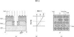
- FIG. 8A shows a cross-sectional view of a sample in which contact holes are formed in a three-layer structure.
- the electron beam 102 irradiates the layer surface of the sample with the electron beam 102 and the layer surface is charged by secondary electrons emitted from each layer.
- FIG. thus, in the charging control method using the electron beam 102, a substantially uniform electric field strength (strength proportional to the slope of the graph of FIG. 8A (b)) is formed from the hole bottom of the hole pattern to the wafer surface.
- FIG. 4B is a diagram showing the relationship between the depth direction of the sample and the potential in the depth direction in a state where the lowermost layer is grounded and the uppermost layer is charged to 10 V by an electron beam.
- the amount of signal from the hole depends on the electric field strength distribution generated in the vertical direction of the hole.
- the electric field strength distribution is uniform from the hole bottom to the surface, secondary electrons from each layer can be obtained uniformly.
- the contrast was weak, and it was difficult to extract only the pattern contrast of a specific layer included in the middle. That is, the pattern contrast between the intermediate layer 104 and the lowermost layer 105 is weak as shown in FIG. 5C, which is a secondary electron image obtained by observing the contact hole from the upper surface of the sample, and it is difficult to clearly identify it.
- FIG. 4A is a cross-sectional view taken along the line AA ′ in FIG.
- the pattern contrast of a specific layer it is important to control the charge distribution from the specific layer to the surface and increase the electric field strength from the specific layer to the surface layer.
- pattern contrast is improved by utilizing conduction by ultraviolet light irradiation, only the sidewall layer can be made conductive and charging can be suppressed.
- sufficient pattern contrast cannot be obtained only by conduction.
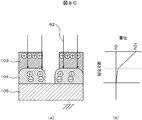
- the intermediate layer is formed by irradiating light 62 that is transmitted through the hole upper layer and absorbed by the intermediate layer as shown in FIG. 8C (a). Only the sidewall layer can be made conductive to suppress charging.
- the electric field strength can be reduced to almost zero by reducing the resistance of the sidewall layer as shown in FIG.
- the electric field strength from the sidewall layer to which the pattern contrast is to be improved to the upper surface of the hole can be made larger than the conventional one ((b) in FIG. 8A), and at the same time, the electric field strength from the sidewall layer to the hole surface is increased. It can be made lower than the conventional one ((b) in FIG. 8A).
- secondary electrons emitted from the sidewall layer are easily drawn out to the detector side, and secondary electrons emitted from the hole surface are hardly drawn out to the detector side, and the pattern contrast is larger than the conventional one. It is considered to be.
- it is possible to improve the pattern contrast compared to the conventional method by conducting the intermediate layer with ultraviolet light there is a problem that it is very difficult to determine the defect because a sufficient pattern contrast cannot be obtained as before.
- An object of the present invention is to solve the above-mentioned problems, and to provide a charged particle beam apparatus that can control charging of a sample having various structures at high speed and stably and detect a specific defect with high sensitivity.
- a typical apparatus of the present invention is as follows.
- the charged particle beam apparatus includes a light irradiation system capable of simultaneously irradiating light in a first wavelength band and light in a second wavelength band, which are different from each other in the same region.
- Another representative apparatus includes a charged particle gun, a sample holder for placing a sample, and a charged particle beam irradiated from the charged particle gun to the sample placed on the sample holder.
- a particle optical system a detector for detecting secondary electrons generated by irradiating the charged particle beam to the sample, and an image processing unit for image processing of the secondary electron signal detected by the detector;
- a light irradiation system for irradiating the sample placed on the sample holder with light, and the light irradiation system integrates the optical paths of the light in the first wavelength band and the light in the second wavelength band having different wavelength bands from each other
- a charged particle beam apparatus including a beam splitter.
- Another representative apparatus is a charged particle beam apparatus that inspects a sample having a structure in which at least a first layer, a second layer, and a third layer are sequentially stacked from above.
- a sample holder for mounting, light in a first wavelength band absorbed by the first layer, and a first light transmitted through the first layer and the second layer and absorbed by the third layer
- a light irradiation system for simultaneously irradiating light in the second wavelength band, the first layer positively charged by irradiation with light in the first wavelength band, and the third layer by irradiation with light in the second wavelength band
- a charged particle optical system that irradiates a charged particle beam emitted from a charged particle gun to the second layer that is negatively charged by the photoelectron and is generated by the photoelectron, and the charged particle beam is the first layer and the second layer.
- a detector for detecting secondary electrons generated by irradiating the layer, and a signal of the secondary electrons detected by the detector.
- a plurality of wavelengths can be irradiated simultaneously, and the pattern contrast can be improved.
- the pattern contrast it is possible to provide an apparatus capable of observation, measurement, and inspection using a highly accurate and sensitive charged particle beam.
- the block diagram which shows an example of the semiconductor inspection apparatus of this invention The block diagram which shows an example of the light irradiation optical system of this invention.
- Explanatory drawing which shows an example of the effect in this invention
- Explanatory diagram showing an example of the effect of the studied technology
- Explanatory drawing which shows the method of determining an irradiation wavelength with an absorptance curve.
- Explanatory drawing which shows an example of the effect of the layer structure of a test object.
- the block diagram which shows the flow which determines irradiation conditions using a database.
- the block diagram which shows GUI which sets light irradiation conditions.
- Explanatory drawing which shows an example of the effect of the layer structure of a test object.
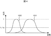
- the wavelength means the wavelength of the peak of the intensity distribution in the output intensity distribution of the light
- the wavelength band means the output of 1 / e or more with respect to the peak output obtained by standardizing the output intensity distribution of the light. Is the range of wavelengths.
- Example 1 In this embodiment, an example will be described in which an alignment failure of an intermediate layer is detected when a hole pattern is formed on a wafer to be inspected as a sample with an electron beam (charged particle beam) apparatus.
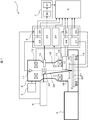
- the electron beam apparatus 1 includes an electron optical system 2, a stage mechanism system 3, a wafer transfer system 4, a vacuum exhaust system 5, a control system 6, an image processing system 7, an operation unit 8, a light irradiation system 9, and a light irradiation condition measurement system 10. It is configured.
- the electron optical system 2 includes an electron gun 11, a condenser lens 12, an objective lens 13, a detector 14, a deflector 15, and an electrode 16 on the wafer.
- the light irradiation condition measurement system 10 includes an absorptivity meter 17 and a surface potential meter 18.
- the stage mechanism 3 includes an XY stage 19, a wafer holder (sample holder) 20, and a wafer 21.
- the control system 6 includes a beam control unit 22, a detection system control unit 23, a deflection control unit 24, an electron lens control unit 25, a retarding voltage control unit 26, an electrode control unit 27, a light irradiation condition measurement control unit 28, and a light irradiation control unit. It is composed of 29.
- the image processing system 7 includes an image processing unit 30 and an image storage unit 31.
- the light 32 introduced into the vacuum in the housing covering the electron optical system is irradiated to the wafer 21 which is the inspection target sample, and at the same time, the electron beam is irradiated, and the defect is detected from the detected secondary electron image. Perform an inspection.
- a configuration example of the light irradiation system 9 is shown in FIG.
- the light source 34 a light source including a wavelength of 133 nm or more and 1064 nm or less was used.
- a mercury lamp, an excimer lamp, a wavelength tunable laser, or the like can be used.
- the light emitted from the light source is split into two lights by splitting the light path of the light into two using the beam splitter 35.
- the divided light can be controlled by changing the wavelength band using the wavelength selection filters 36 and 37 disposed in the respective optical paths.
- An etalon filter was used as the filter.
- An etalon filter is a general filter that can select a wavelength according to the angle of light incident on the filter. These filters can individually control the angle with respect to the incident light, and can set the wavelength band for each light divided by the control from the light irradiation control unit 29.
- the wavelength selection filters 36 and 37 use etalon filters having different filter widths, and the wavelength selection width is changed by changing the selection wavelength range. In this embodiment, an etalon filter is used. However, a combination of wavelength selection filters and a spectroscopic element can be used, and the present invention is not limited to this embodiment.
- light energy control elements 38 and 39 are arranged in the respective optical paths, and continuous ND (Neutral-Density) filters are used as these control elements.
- the continuous ND filter is a filter whose transmittance varies depending on the position of light to be irradiated, and energy can be controlled by moving the filter position. Not only a continuous type but also a revolver type ND filter can be used. In this embodiment, an ND filter is used. However, an attenuator or a wedge plate can be used, and the present invention is not limited to this embodiment.
- shutters 40 and 41 for shielding light are arranged in the respective light paths.
- the irradiation time of light passing through each optical path and the presence or absence of irradiation can be controlled by opening and closing the shutters 40 and 41.
- An optical chopper can also be used as a device for controlling the irradiation time.
- These wavelength selection filter, energy adjustment element, and shutter can be controlled independently by the light irradiation controller 29.
- the individually set light is integrated into one optical path by the beam splitter 42, and the beam shape of the light to be irradiated can be collectively controlled using the beam shape control element 43.
- a microlens array is used for the beam shape control element 43.
- the beam shape can be arbitrarily set regardless of the electron beam scanning region.
- Other beam shape control elements include a down collimating optical system using a mirror lens, and the present embodiment is not particularly limited to a microlens array or a down collimating optical system.
- the light emitted from the single light source is branched by the beam splitter 35, and after the wavelength band, energy, and presence / absence of irradiation of each branched light are controlled, the light path is changed by the beam splitter 42. It is configured so that the inspection sample (wafer) in the vacuum can be irradiated as light 32.
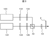
- FIG. 2 a configuration example of a light irradiation system 9 different from that shown in FIG. 2 is shown in FIG.
- two types of light sources 130 and 131 for example, a halogen lamp and a mercury lamp
- Control elements 132 and 133 and shutters 134 and 135 are included. Since the configuration and role of each energy control element and shutter have been described with reference to FIG. 2, description thereof is omitted here.
- laser light is used as the light source, there are a method using higher-order wavelength conversion and a method using parametric oscillation.
- One type of light source may be provided as 130 and 131, and wavelength selective filters 36 and 37 may be provided as shown in FIG.
- Light 32 is introduced into a vacuum using a high transmittance vacuum window to ultraviolet region, such as quartz or MgF 2.
- the light introduced into the vacuum can be incident on the wafer substantially coaxially with the electron optical system by the reflector 33 installed on the axis of the electron optical system 2.
- the reflecting plate 33 is configured by applying an aluminum coating or a coating with high reflectivity by a dielectric multilayer film. In this embodiment, an optical system that vertically irradiates light is employed.
- the absorptivity meter 17 that measures the absorptance of each layer formed on the wafer is configured to measure the amplitude and polarization angle of the light when the irradiated light is reflected by the wafer.
- the absorption coefficient can be calculated from the measurement results of the amplitude and the polarization angle based on the principle of spectroscopic ellipsometry.
- a spectroscope is used as means for measuring the amplitude of light for each wavelength, and the polarization angle can be measured using a polarizer.
- the surface potential system 18 a non-contact surface potential meter was used.
- the absorptivity meter 17 is not an indispensable component of the present apparatus. For example, there are cases where the absorption coefficient has already been measured outside the apparatus and is already known, or the absorption coefficient is empirically determined by process conditions. . In this case, it is not necessary to determine the absorption coefficient in a vacuum in the inspection apparatus, and the absorption rate meter 17 can be omitted from the apparatus configuration. Further, as an example of the light irradiation system, an example in which a beam splitter 42 for integrating optical paths as shown in FIGS. 2 and 3 is provided.
- the beam splitter 42 may not be provided. It is also possible to adopt a configuration in which different light sources are used and the light is incident on the wafer from different directions. In other words, any light irradiation system capable of simultaneously irradiating light having different wavelength bands to a predetermined same region on the surface of the wafer may be used, and the optical paths may not be integrated before being irradiated into the vacuum. However, when the optical paths are integrated, it is not necessary to control the light irradiation area and the beam shape control element independently, so that there is an advantage that the light irradiation control can be easily and highly accurately performed. .
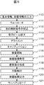
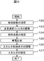
- FIG. 5 shows an inspection flow.
- the basic information of the wafer includes a layout pattern and the inspection information includes an inspection area, an inspection condition, and a light irradiation condition.
- Inspection conditions include an electron beam current to be irradiated, incident energy, scanning speed, and scanning area.
- the light irradiation conditions include wavelength, irradiation energy, irradiation pulse, irradiation region, light absorption rate of the material to be inspected, etc. (step 110).
- the wafer 21 is introduced into the preliminary sample chamber (not shown) by the transfer system 4 and evacuated and then introduced into the inspection chamber ( Step 111).
- the light irradiation control unit 29 sets the light irradiation condition based on the light irradiation condition which is the inspection information input in step 111 (step 112).
- the electron beam irradiation conditions are set based on the inspection conditions input in step 112. At the time of this setting, the electron beam focal point, astigmatism, and the like are also calibrated using the electron beam calibration pattern (step 113). After calibration of the electron beam, the wafer position is detected, and the wafer position and rotation amount are aligned (step 114). After the alignment, the shutters 40 and 41 in the light irradiation system 9 are opened, and adjustment of the brightness and contrast of the secondary electron image acquired by the detection system 14 while irradiating light, so-called calibration is performed (step 115).
- step 116 inspection is started based on the inspection area (step 116), the shutters 40 and 41 in the light irradiation system 9 are opened, and light is emitted from the irradiated area by moving the stage while irradiating light.
- the secondary electron image is acquired as an inspection image (step 117).
- the image processing system 7 acquires secondary electron images from two identical pattern layout portions in different areas, and performs image comparison inspection using one of the secondary electron images as a reference image corresponding to a normal portion and the other as an inspection image.
- the difference image of each image is acquired (step 118).
- both images need not be secondary electron images, and a difference image may be acquired using CAD data as a reference image.
- a defect position is extracted from the abnormal brightness of the difference image (step 119), and an inspection result is output (step 120). That is, when the difference signal of the difference image is equal to or greater than a certain value, it is determined that the position of the difference signal is defective. On the other hand, when the difference signal is less than the certain value, it is assumed that there is no defect. Determined. In this way, the presence or absence of a defect is determined from the value of the difference signal of the difference image, that is, the abnormal brightness, and is output as the inspection result. After the inspection is completed, the wafer 21 is unloaded by the transfer system 4 and the process is completed (step 121).
- the wafer 32 is irradiated with light 32, and the absorption rate (absorption coefficient) is measured by the absorption rate meter 17 (step 122).
- the filter angle of the wavelength selection filters 36 and 37 is changed by a signal from the light irradiation control unit 29 so as to be equal to or less than the absorption rate set in the light irradiation condition, and the wavelength band of each light to be irradiated is adjusted (step 123).
- the irradiation wavelength is set (step 124).
- the irradiation energy is calibrated by measuring the surface potential of the irradiation area with the surface potentiometer 18 (step 125) and setting the light energy control elements 38 and 39 to the light irradiation control unit so as to satisfy the surface potential set in the light irradiation conditions. Rotate at 29 to adjust and set the irradiation energy (steps 126, 127). In addition, the light irradiation area is also adjusted in this series of flows. Thereafter, electron beam irradiation conditions are set (step 113). As described above, when the light absorption rate of the material to be inspected is known, the measurement of the absorption rate can be omitted.
- each member of the light irradiation system 9 is controlled through the light irradiation control unit 29, and the light wavelength band, irradiation energy, and irradiation region suitable for the inspection wafer are set. Further, the presence / absence of irradiation of light of different wavelength bands and the irradiation time can also be set by controlling the shutter of the light irradiation control unit 29.
- FIG. 7 shows the layer structure of a sample wafer.
- the surface layer 44 has a three-layer structure of an intermediate layer 45 and a lowermost layer 46.
- the surface layer 44 is SiO 2
- the intermediate layer 45 is Si 3 N 4
- the lowermost layer 46 is Si.
- This drawing SiO 2 is selectively etched using the resist pattern pattern of the contact hole is formed on the SiO 2 surface layer 44 as a mask, after further Si 3 N 4 intermediate layer 45 is selectively etched It is sectional drawing of the wafer at the time of contact hole formation.
- this is a well-known layer structure used when a contact is made with a diffusion layer to a transistor of a DRAM memory cell.
- the Si 3 N 4 intermediate layer 45 by selective etching to be smaller than the hole diameter of the SiO 2 surface layer 44, than the hole diameter of the SiO 2 surface layer 44 the Si 3 N 4 intermediate layer 45 The hole diameter is shown to be small.
- FIG. 8A shows the potential distribution on the hole axis (see FIG. 8A (b)) and the resulting secondary electron image (see FIG. 8A (c)) when the electron beam 102 is irradiated to charge the sample surface.
- charge formation with an electron beam charges are accumulated on the surface of the sample. Therefore, the potential gradient from the intermediate layer 104 to the surface layer 103 is weak, and the electric field strength is small. Therefore, the contrast of the region 49 showing the intermediate layer in the hole in the secondary electron image is weak, and pattern recognition is difficult.
- FIG. 8A shows the potential distribution on the hole axis (see FIG. 8A (b)) and the resulting secondary electron image (see FIG. 8A (c)) when the electron beam 102 is irradiated to charge the sample surface.
- the potential gradient from the intermediate layer 104 to the surface layer 103 is weak, and the electric field strength is small. Therefore, the contrast of the region 49 showing the intermediate layer in the hole in the secondary electron image is weak, and pattern recognition is difficult.
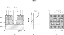
- FIG. 8B is a schematic diagram of a sample cross section when the light irradiation of a plurality of wavelength bands is performed by the charged particle beam apparatus of the present invention, the potential distribution on the Hall axis (see FIG. 8B (b)), and the obtained secondary.
- An electronic image see FIG. 8B (c) is shown.
- light 50 in the first wavelength band having a wavelength absorbed by the surface layer 103, the surface layer 103, and the intermediate layer 104 are transmitted and absorbed by the lowermost layer 105.
- the sample is irradiated with second light 51 having a wavelength band different from the first wavelength band.
- the light of the first wavelength band is absorbed by the surface layer 103 to form a positive charge on the surface layer 103, and the light of the second wavelength band is absorbed by the lowermost layer 105 to absorb photoelectrons from the lowermost layer 105.
- the photoelectrons are emitted and injected into the intermediate layer 104, thereby negatively charging the intermediate layer 104.
- FIG. 8B (b) shows the relationship between the sample depth direction and the charged potential when such a phenomenon occurs and the surface layer 103 is positively charged and the intermediate layer 104 is negatively charged. This figure is a relationship diagram when the surface of the surface layer 103 is positively charged to 10V.
- the intermediate layer 104 is negatively charged, so that the potential in the layer becomes negative compared to the lowermost layer 105 at a specific location (for example, ⁇ 2 V). Therefore, the potential gradient from the intermediate layer 104 to the surface layer 103 is larger than the conventional potential gradient, and the electric field strength can be larger than the conventional one.
- the potential gradient from the lowermost layer 105 to the intermediate layer 104 can be a negative gradient, and the direction of the electric field can be reversed.
- the potential gradient from the lowermost layer 105 to the intermediate layer 104 can be a negative gradient, and the direction of the electric field can be reversed.
- the contrast between the region 104 indicating the intermediate layer in the hole and the region 105 indicating the lowest layer in the hole is increased, and the defective portion 106 that is poorly aligned is obtained in the prior art. It can be easily recognized as compared to the secondary electron image. As a result, defects in the intermediate layer can be detected with high sensitivity.
- the shutters 40 and 41 switch the presence / absence of irradiation of the light in the first wavelength band and the light in the second wavelength band with the shutters 40 and 41, thereby changing the first wavelength. It is possible to inspect the surface layer 103 by positively charging the surface layer 103 with band light, and to inspect the intermediate layer 104 by simultaneously irradiating light in the first and second wavelength bands. It is also possible to perform defect inspection of different layers with this apparatus by switching the presence or absence of irradiation from the design data.
- the surface layer 103 is SiO 2
- the intermediate layer 104 is Si 3 N 4
- the lowermost layer 105 is Si.
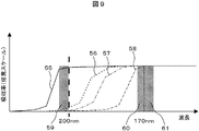
- the absorption rate was measured by the absorption rate meter 17 using the configuration of this example.
- the vertical axis represents the normalized absorption rate of an arbitrary case, and the horizontal axis represents the wavelength. The higher the absorption rate, the easier the light having a specific wavelength is absorbed.
- the horizontal axis is the axis whose wavelength increases as it goes to the left.
- This measurement result shows that the light absorptance depends on the wavelength depending on the material, and also shows that the light absorptance depends on the wavelength depending on the film formation method even for the same material. I understand.
- the light of the first wavelength band selects the wavelength band 60 of 170 to 180 nm, and when the surface layer 103 is created by thermal oxidation, the first wavelength As the band light, a wavelength band 61 of 133 to 170 nm is selected.
- the wavelength band 59 of 200 to 220 nm is selected.
- the wavelength band to be selected is determined by the relationship between the wavelength and the absorptance.
- a wavelength band having a high absorption rate that is easily absorbed by the surface layer 103 is selected, and as the light in the second wavelength band, the surface layer 103 and the intermediate layer 104 are selected.
- a wavelength band that is not easily absorbed (is easily transmitted), has a low absorption rate, and is easily absorbed by the lowermost layer 105 is selected.
- the measurement of the absorptance and the result were demonstrated, as above-mentioned, it is not necessary to measure an absorptivity with this apparatus, and the combination of the wavelength band suitable for the relationship between the absorptivity and the wavelength of each layer, or this inspection. If known, the first wavelength band and the second wavelength band can be determined using known information.
- the irradiation energy setting for each wavelength band in step 126 will be described here. While irradiating only the light in the first wavelength band and measuring the surface potential using the charging potentiometer 18, the irradiation energy is adjusted so as to reach the target charging potential. Thereafter, the light of the second wavelength band is irradiated, and the irradiation energy of the second light is adjusted so that the pattern contrast of the layer to be detected is greater than or equal to a certain value. In this way, the surface potential can be set to the target value by adjusting in two steps, such as the adjustment of the irradiation energy of the light in the second wavelength band after the adjustment of the irradiation energy of the light in the first wavelength band. It is possible to adjust the irradiation energy of light so as to obtain a satisfactory pattern contrast.
- the light irradiation system 9 has a structure in which the combination of the first wavelength band and the second wavelength band can be changed in order to support an arbitrary layer structure. .
- the structure can change the combination of the first wavelength band and the second wavelength band. .
- the irradiation energy can be set independently.
- wavelength bands when inspecting a sample having a specific layer structure or a structure having only a specific film formation method, it is suitable for the layer structure in advance without changing the wavelength band combination. It can also be fixed to a combination of different wavelength bands.
- the first wavelength band is within a range of 133 to 180 nm. What is necessary is just to set it as the combination of a predetermined wavelength band and the light of a predetermined wavelength band from the range of 200 to 220 nm as a 2nd wavelength band.
- the wavelength range of light is assumed to be a wavelength with a peak wavelength of 100 nm to 1064 nm in consideration of materials used in semiconductors. The effects of the present invention can be obtained even when a laminated film is formed with layers of various materials.
- the first wavelength band 100 and the second wavelength band light 101 are light including a plurality of long and short wavelengths with a peak wavelength as shown in FIG. 4 as the center.
- a broad wavelength band having a wavelength width of several tens to several hundreds of nm, or light having a narrow wavelength band of several nm to several tens of nm such as laser light can be used.
- the wavelength band in the output range of 1 / e or more with respect to the standardized peak output is shown.
- light having different wavelength bands means light in a wavelength band that does not overlap each other with an output of 1 / e or more with respect to the peak output of each light.
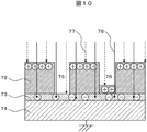
- FIG. 10 shows the layer structure of the wafer to be inspected.
- a surface layer 72, an intermediate layer 73, and a lowermost layer 74 have a three-layer structure.
- the surface layer 72 is a resist film
- the intermediate layer 73 is an antireflection film (BARC)
- the lowermost layer 74 is Si.
- the sample differs from the sample described in Example 1 in that the intermediate layer 73 is not opened.
- the alignment defect inspection has been described.
- the second embodiment is an example adapted to the inspection of the defective opening.
- the normal portion 75 is exposed and opened leaving the BARC layer, and the defect portion 76 shows a state of defective opening because the resist film remains.
- both the resist layer and the BARC layer are insulative, and are similarly charged. Therefore, the hole bottom is charged in both the normal part and the defective part.
- it is a secondary electron image with almost no difference in brightness only by the charge control method using an electron beam. It was difficult to obtain contrast.
- the defect contrast can be improved by using the light 77 in the first wavelength band and the light 78 in the second wavelength band of the apparatus described in the first embodiment for this defective opening.
- the light 77 in the first wavelength band selects light in the wavelength band that is easily absorbed by the surface layer 72, and the light 78 in the second wavelength band is hardly absorbed by the surface layer 72 and the intermediate layer 73 (is easily transmitted). And light having a wavelength band that is easily absorbed by the lowermost layer 74 is selected.
- the surface layer 72 can be positively charged and the intermediate layer 73 can be negatively charged. In the prior art, it is difficult to obtain defect contrast because the normal part and the defective part are positively charged.
- the normal part can be negatively charged and the defective part can be positively charged. Therefore, secondary electrons from the normal part are easily drawn out to the detector side, the contrast with the defective part is improved, and the defect of the opening defect can be detected with high accuracy.
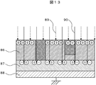
- Example 3 the inspection of a sample to be inspected, which is different from the first and second embodiments, will be described using the apparatus described in the first embodiment.
- the layer structure of the wafer is shown in FIG.
- the surface layer 86 has a three-layer structure of an intermediate layer 87 and a lowermost layer 88.
- the surface layer 86 is SiO 2
- the intermediate layer 87 is a diffusion (bonding) layer
- the lowermost layer 88 is Si.
- the intermediate (bonding) layer 87 is a diffusion layer and a plug is embedded in the contact hole.
- the alignment defect inspection is described.
- the opening defect inspection is described.
- the third embodiment is an example adapted to the detection of the plug short defect of the wafer on which the plug pattern is formed.
- the normal portion is a plug portion embedded in the surface layer 86 on the left side of FIG. 13 and the plug and the intermediate layer 87 are electrically connected.
- the defective portion is a plug portion embedded in the surface layer 86 on the right side of the figure, and the plug is not electrically connected to the intermediate layer 87 because the plug is embedded in the contact hole having a defective opening. .
- the defect contrast can be improved by using the light 89 in the first wavelength band and the light 84 in the second wavelength band of the apparatus described in the first embodiment for this plug short defect.
- the light in the first wavelength band is selected from the light in the wavelength band that is easily absorbed by the surface layer 86, and the light 90 in the second wavelength band is difficult to be absorbed by the surface layer 86 (is easily transmitted) and is intermediate.
- Light having a wavelength band that is easily absorbed by the layer 87 is selected.
- photoelectrons can be emitted from the surface layer, the surface can be positively charged, and the intermediate layer 87, which is a junction, can be obtained using light 84 in the second wavelength band.
- the charging of the plug in the defective part it is difficult for the charging to be eased because electrons do not easily flow due to a defect. Therefore, when the electron beam for inspection is irradiated due to the difference in charge amount, the detected amount of secondary electrons emitted from the plug surface is different, and the brightness difference between the normal part and the defective part can be obtained. And the defect portion are improved, and defects such as plug short-circuit defects can be detected with high accuracy.
- the energy of the light 90 in the second wavelength band is adjusted first to adjust the conductive energy of an appropriate bonding layer. Whether the bonding layer is conductive or not is determined by measuring the current flowing through the bonding layer using a current meter mounted on the retarding voltage control unit 26 to determine whether the energy is appropriate.
- the light 89 in the first wavelength band is irradiated while irradiating the light 90 in the adjusted second wavelength band, and the light 89 in the first wavelength band is set so that the pattern contrast is greater than or equal to a certain value. The energy is adjusted.
- Example 4 a means for selecting a wavelength band of light irradiated by the apparatus described in Embodiment 1 will be described.
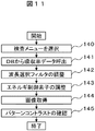
- the selection flow of the wavelength band of the irradiation light when the information on the absorptivity for each layer material is previously databased will be described.
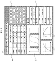
- FIG. 12 shows a GUI (Graphical User Interface) registered in the workstation mounted on the operation unit 8.
- the type of defect to be inspected can be input. For example, an opening failure or alignment failure.
- the layer structure of the sample to be inspected can be input. For example, a three-layer structure or a four-layer structure.
- a layer to be inspected can be input. For example, a surface layer and an intermediate layer.
- the layer structure and the induced phenomenon are registered and automatically called to the layer structure setting window 80 (step 140).
- “Photoelectron” indicates that light is absorbed by the corresponding layer
- “transmission” indicates that light is transmitted by the corresponding layer.
- the absorption rate data is called from the database in which the absorption rate for each material is registered in advance (step 141), and the filter angles of the wavelength selection filters 36 and 37 are changed by a signal from the light irradiation control unit 29. (Step 142).
- the irradiation amount is calculated from the quantum efficiency registered in the database and the irradiation area of each wavelength band, and the light energy control elements 38 and 39 are rotated from the light irradiation control unit 29 to determine the energy (step 143). ). Further, a secondary electron image 84 is acquired, and it is confirmed by image analysis that a desired pattern contrast is obtained.
- the absorptance data display window 81 displays each absorptance data (for example, wavelength-absorptivity data in FIG. 9), and the wavelength band irradiated on the display window can be adjusted.
- each absorptance data for example, wavelength-absorptivity data in FIG. 9
- the wavelength band irradiated on the display window can be adjusted.
- the pattern contrast of the layer to be inspected is insufficient, the energy is adjusted. The energy adjustment is determined from the charge amount and the pattern contrast as described in the first embodiment.
- the energy of light in the first wavelength band is set so that the potential falls within an error range of 0.5 V or less with respect to the set charging potential.
- the energy of light in the second wavelength band is adjusted while measuring the pattern contrast, and the maximum value at which the pattern contrast is maximized is determined and set.
- the energy of light in the second wavelength band may be adjusted first depending on the layer structure of the inspection sample and the inspection defect to be processed.
- the setting result is displayed in the charge amount data display window 82 and the pattern contrast data display window 83.
- the charge amount of the layer can be grasped from the charge amount data display window.
- the pattern contrast data display window shows the dependence of the contrast energy on the energy of the light so that the contrast in the adjusted energy of the light is an appropriate contrast or the energy of the light that further improves the contrast. It is possible to grasp whether there is.
- the charge amount data display and pattern contrast data display can confirm the increase in irradiation energy amount and the deterioration of the light source and optical system from abnormal characteristic curves.
- the degraded optical path can be identified depending on whether there is an abnormality.
- the condition of the irradiating light is displayed in the condition result display window 85 and incorporated in the inspection flow.
- the secondary electron image 84 is displayed in real time as a GUI. Therefore, it is possible to grasp the contrast state of the secondary electron image 84 in the result of the condition of the light to be irradiated. Further, in the condition result display window 85, the operator can input an arbitrary numerical value, and the light irradiation system 9 can be controlled by the input number. Further, the secondary electron image 84 under the input conditions is also displayed in real time, so that the contrast can be adjusted.
- the inspection for the defective opening in the second embodiment will be described as an example.
- the defect type setting window 79 a mode for inspecting a defective opening of a wafer having a three-layer structure was selected, and in the layer structure setting window 80, a three-layer structure of resist, BARC, and Si was selected.
- the phenomenon induced by light for each layer is configured to be automatically determined by the type of defect and the designation of the layer, but can be changed by the operator in the layer structure setting window 80.
- the wavelength at which photoelectrons are emitted from the resist the wavelength absorbed by the resist
- the surface layer is positively charged.
- the Si layer absorbs the light in the second wavelength band, thereby releasing photoelectrons from the Si layer and negatively charging the BARC layer. And a method of making the BARC layer conductive by absorbing light in the second wavelength band.
- the absorption rate data display window 81 can call up and display the absorption rate data for each material and manufacturing method registered from the database.
- the results measured with the absorptivity meter 17 and the surface potential meter 18 for each material and manufacturing method, and data disclosed by the material manufacturer are registered in the database.
- the absorption data shows that the wavelength that makes BARC conductive is high in the resist, so it is difficult for the resist to absorb, and there is no appropriate wavelength that is easily absorbed by BARC. It can be judged that improvement cannot be expected.
- the wavelength of light that passes through the resist and BARC and is absorbed by Si and emits photoelectrons from Si has a low absorptance at resist and BARC, and can effectively suppress the charging of BARC. It can be judged from the absorption rate data displayed in 81. For this reason, a wavelength that transmits the resist and BARC as light in the second wavelength band, is absorbed by Si, and emits photoelectrons from Si is selected.
- the wavelength bands of the first light and the second light are automatically extracted from the absorptivity database.
- the first light is light in the wavelength band of 160 to 180 nm
- the second light is 240 to 300 nm. It became light of the wavelength band.
- Examples 1 to 4 have been described.
- the wavelength band to be selected is selected from an ultraviolet region of 100 nm to 400 nm or less absorbed by SiO 2 or Si, visible light of 400 nm to 700 nm or less that transmits SiO 2, and a near infrared of 700 nm to 1100 nm or less that transmits Si.
- the pattern contrast can be controlled according to the layer from which the defect is to be extracted and the type of the defect to be detected.
- the absorptance changes depending on the material constituting the wafer layer and the manufacturing method, there is a problem that it is difficult to select the light irradiation conditions. Therefore, means for measuring the absorption rate of each layer and means for measuring the charge amount formed by light irradiation are provided.
- the wavelength band to irradiate can be selected according to the result of the absorptance measured for each wavelength for each layer.
- the irradiation energy can be controlled according to the measurement result of the charge amount of the light irradiation unit, the stability and reproducibility of the pattern contrast can be improved.
- Electron beam apparatus 2 ... Electro-optic system, 3 ... Stage mechanism system, 4 ... Wafer conveyance system, 5 ... Vacuum exhaust system, 6 ... Control system, 7 ... Image processing system, 8 ... Operation part, 9 ... Light irradiation System: 10 ... Light irradiation condition measurement system, 11 ... Electron gun, 12 ... Condenser lens, 13 ... Objective lens, 14 ... Detector, 15 ... Deflector, 16 ... Electrode on wafer, 17 ... Absorbance meter, 18 ... Surface potentiometer, 19 ... XY stage, 20 ... Wafer holder, 21 ... Wafer, 22 ... Beam control unit, 23 ...
- defect type setting window 80 ... layer structure 81 ... Absorption rate data display window, 82 ... Charge amount data display window, 83 ... Pattern contrast data display window, 84 ... Secondary electron image, 85 ... Condition result display Window, 86 ... Surface layer, 87 ... Intermediate layer, 88 ... Bottom layer, 89 ... First wavelength band, 90 ... Second wavelength band, 100 ... First wavelength band, 101 ... Second wavelength Wavelength band, 102 ... electron beam, 103 ... surface layer, 104 ... intermediate layer, 105 ... bottom layer, 106 ... defect, 130 ... light source, 131 ... light source, 132 ... energy control element, 133 ... energy control element, 134 ... Shutter, 135 ... Shutter.
Landscapes
- Chemical & Material Sciences (AREA)
- Analytical Chemistry (AREA)
- Testing Or Measuring Of Semiconductors Or The Like (AREA)
- Analysing Materials By The Use Of Radiation (AREA)
Abstract
Description
(実施例1)
本実施例では、電子線(荷電粒子線)装置で、試料として被検査ウェハにホールパターンが形成されている場合の、中間層のアライメント不良を検出する一例について述べる。本実施例における電子線装置の構成例を図1に示す。電子線装置1は電子光学系2、ステージ機構系3、ウェハ搬送系4、真空排気系5、制御系6、画像処理系7、操作部8、光照射系9、光照射条件測定系10により構成されている。電子光学系2は、電子銃11、コンデンサレンズ12、対物レンズ13、検出器14、偏向器15、ウェハ上の電極16により構成されている。光照射条件測定系10は吸収率計17、表面電位計18により構成されている。ステージ機構系3はXYステージ19、ウェハホルダ(試料ホルダ)20、ウェハ21により構成されている。制御系6はビーム制御部22、検出系制御部23、偏向制御部24、電子レンズ制御部25、リターディング電圧制御部26、電極制御部27、光照射条件測定制御部28、光照射制御部29により構成されている。画像処理系7は画像処理部30、画像記憶部31により構成されている。
図5に検査フローを示す。操作部8から、あらかじめ作成、登録したウェハの基本情報、検査情報を入力する。ウェハの基本情報はレイアウトパターン等があり、検査情報は検査領域、検査条件、光照射条件がある。検査条件は照射する電子ビーム電流、入射エネルギ、走査速度、走査領域がある。光照射条件は波長、照射エネルギ、照射パルス、照射領域、検査対象となる材料の光の吸収率等がある(ステップ110)。ウェハの基本情報、検査情報の入力(検査条件設定)の後、ウェハ21は搬送系4により、予備試料室(図示せず)に導入され、真空排気された後に、検査室に導入される(ステップ111)。ウェハロード後、ステップ111で入力した検査情報である光照射条件に基づき光照射制御部29により光の照射条件が設定される(ステップ112)。
(実施例2)
本実施例では、実施例1で説明した装置を用いて、実施例1とは異なる検査対象の試料の検査について説明する。検査対象となるウェハの層構造について図10示した。表面層72、中間層73、最下層74の三層構造で構成されており、表面層72はレジスト膜、中間層73は反射防止膜(BARC)、最下層74はSiである。中間層73が開口していない点において、実施例1で説明した試料とは異なる。実施例1ではアライメント欠陥の検査について説明したが、本実施例2では開口不良の検査に適応した例である。正常部75はBARC層を残して露出され開口している状態であり、欠陥部76はレジストの膜が残存しており開口不良の状態を示している。通常の電子線による帯電ではレジスト層もBARC層も絶縁層であるため同様に帯電する。そのため、正常部、欠陥部ともに穴底が帯電することになる。開口不良の検査の場合には、穴底の帯電の有無によって正常部と欠陥部の明度差を得るため、電子線を用いた帯電制御法のみではほとんど明度差がない二次電子画像であり欠陥コントラストを得ることが困難であった。
(実施例3)
本実施例では、実施例1で説明した装置を用いて、実施例1及び2とは異なる検査対象の試料の検査について説明する。ウェハの層構造について図13に示した。表面層86、中間層87、最下層88の三層構造で構成されており、表面層86はSiO2、中間層87は拡散(接合)層、最下層88はSiである。中間(接合)層87が拡散層である点及びコンタクトホールにプラグが埋め込まれている点において、実施例1及び2で説明した試料とは異なる。実施例1ではアライメント欠陥の検査、実施例2では開口不良の検査について説明したが、実施例3ではプラグパターンが形成されているウェハのプラグショート不良の検出に適応した例である。正常部は図13左側の表面層86に埋め込まれたプラグ部分でありプラグと中間層87とが電気的に接続されている。一方、欠陥部は図右側の表面層86に埋め込まれたプラグ部分であり開口不良のコンタクトホールにプラグが埋め込まれた状態になっているためプラグと中間層87とが電気的に接続されていない。
(実施例4)
本実施例では、実施例1で説明した装置の照射する光の波長帯の選択手段について、説明する。この実施例では特に吸収率計17を用いる代わりに、層材料毎の吸収率の情報を予めデータベース化した場合における照射光の波長帯の選択フローについて説明する。データベースを用いることで、二次電子画像の取得の際に逐一所定の材料における光の吸収率を測定することなく光照射系9の制御をデータベースに蓄積された情報に基づき高いコントラストの二次電子画像の取得を行うことができる。この選択フローを図11に示す。また、操作部8に搭載されているワークステーションに登録されているGUI(Graphical User Interface)を図12に示す。
図12に示す欠陥種類の設定ウィンドウ79で、検査する欠陥の種類を入力することができるようになっている。例えば開口不良やアライメント不良などである。また、検査する試料の層構造が入力することができるようになっている。例えば三層構造、四層構造などである。また、検査対象となる層を入力することができるようになっている。例えば表面層、中間層などである。このように、検査する欠陥の種類と層の指定ができるようになっている。そして、その欠陥の種類や工程に応じて、層構造や誘起現象が登録されており、層構造の設定ウィンドウ80に自動的に呼び出される(ステップ140)。なお、「光電子」は対応する層で光が吸収されることを示し、「透過」は対応する層で光が透過することを示す。そして、予め装置と接続され、材料毎の吸収率が登録されているデータベースから吸収率データを呼び出し(ステップ141)、波長選択フィルタ36、37のフィルタ角度を光照射制御部29からの信号により変更する(ステップ142)。エネルギ調整はデータベースに登録されている量子効率と各波長帯の照射面積から照射量を算出し、光照射制御部29から光のエネルギ制御素子38、39を回転させ、エネルギを決定する(ステップ143)。さらに二次電子画像84を取得し、所望のパターンコントラストが得られていることを画像解析により確認する。
設定時の結果は帯電量データ表示ウィンドウ82、パターンコントラストデータ表示ウィンドウ83に表示される。帯電量データ表示ウィンドウのより、層の帯電量が把握できるようになっている。また、パターンコントラストデータ表示ウィンドウにより、コントラストの光のエネルギの依存性が分かるようになっており、調整された光のエネルギにおけるコントラストが適切なコントラストとなっているか、さらにコントラストを向上させる光のエネルギが存在するかを把握できるようになっている。また、帯電量のデータ表示やパターンコントラストのデータ表示によって、照射エネルギ量の増加や、異常な特性カーブから光源や光学系の劣化を確認することができ、帯電量データとパターンコントラストデータのどちらに異常があるかによって、劣化している光路を特定することができる。照射する光の条件は条件結果表示ウィンドウ85に表示され、検査フローの中に組み込まれる。
Claims (20)
- 荷電粒子銃と、
試料を載置するための試料ホルダと、
前記試料ホルダに載置された該試料に前記荷電粒子銃から照射される荷電粒子線を照射する荷電粒子光学系と、
該荷電粒子線が該試料に照射されることにより発生する二次電子を検出する検出器と、
前記検出器により検出される該二次電子の信号を画像処理する画像処理部と、
前記試料ホルダに載置された該試料の同一領域に互いに波長帯の異なる第1の波長帯の光と第2の波長帯の光とを同時に照射可能な光照射系とを備えることを特徴とする荷電粒子線装置。 - 請求項1記載の荷電粒子線装置において、
前記光照射系は、前記第1の波長帯の光と前記第2の波長帯の光の光路を統合するビームスプリッタを備えることを特徴とする荷電粒子線装置。 - 請求項1記載の荷電粒子線装置において、
前記第1の波長帯と前記第2の波長帯との波長帯の組み合わせは、変更可能であることを特徴とする荷電粒子線装置。 - 請求項1記載の荷電粒子線装置において、
前記第1の波長帯の光と前記第2の波長帯の光は、それぞれの光のピーク出力に対し1/e以上の出力で互いに重ならない波長帯の光であることを特徴とする荷電粒子線装置。 - 請求項4記載の荷電粒子線装置において、
前記第1の波長帯の光と前記第2の波長帯の光は、それぞれ133nm以上180nm以下、200nm以上266nm以下の波長帯の光であることを特徴とする荷電粒子線装置。 - 請求項1記載の荷電粒子線装置において、
前記光照射系は、光源と、前記光源から放出された光の光路を分岐する第1のビームスプリッタと、前記第1のビームスプリッタにより分岐された夫々の光の光路に設けられた波長帯の変更を行うフィルタと、前記夫々の光の光路を統合する第2のビームスプリッタとを備え、前記第1の波長帯の光と前記第2の波長帯の光は、前記第2のビームスプリッタから照射される光であることを特徴とする荷電粒子線装置。 - 請求項6記載の荷電粒子線装置において、
前記第1のビームスプリッタと前記第2のビームスプリッタとの間の前記第1の波長帯の光と前記第2の波長帯の光の光路の夫々に、光の出力エネルギを調節するフィルタと、光を遮蔽するシャッタとを備えることを特徴とする荷電粒子線装置。 - 請求項1記載の荷電粒子線装置において、
さらに、前記光照射系から照射される光により該試料の所定の層における光の吸収率を測定する吸収率計を備えることを特徴とする荷電粒子線装置。 - 請求項1記載の荷電粒子線装置において、
さらに、該試料を構成する層情報を入力する表示装置と、前記第1の波長帯と前記第2の波長帯との組み合わせを制御する光照射制御部を有し、前記表示装置により入力された層情報に基づき、前記光照射制御部は、前記第1の波長帯と前記第2の波長帯とが所望の組み合わせとなるよう前記光照射系を制御することを特徴とする荷電粒子線装置。 - 請求項9記載の荷電粒子線装置において、
さらに、所定の層材料と光の波長に対する吸収率との情報を蓄積されたデータベースを有し、前記光照射系の制御は、前記データベースに蓄積された該情報に基づき行われることを特徴とする荷電粒子線装置。 - 請求項1記載の荷電粒子線装置において、
前記第1の波長帯の光と前記第2の波長帯の光の一方は、該試料に含まれる所定の層の対して負帯電させる光であることを特徴とする荷電粒子線装置。 - 荷電粒子銃と、
試料を載置するための試料ホルダと、
前記試料ホルダに載置された該試料に前記荷電粒子銃から照射される荷電粒子線を照射する荷電粒子光学系と、
該荷電粒子線が該試料に照射されることにより発生する二次電子を検出する検出器と、
前記検出器により検出される該二次電子の信号を画像処理する画像処理部と、
前記試料ホルダに載置された該試料に光を照射する光照射系とを備え、
前記光照射系は、互いに波長帯の異なる第1波長帯の光と第2波長帯の光との光路を統合するビームスプリッタを備えることを特徴とする荷電粒子線装置。 - 請求項12記載の荷電粒子線装置において、
前記光照射系は、光源と、前記光源から放出された光の光路を分岐する前記ビームスプリッタとは異なる第2のビームスプリッタと、前記第2のビームスプリッタにより分岐された夫々の光の光路に設けられた波長帯の変更を行うフィルタと、を備え、前記光照射系は、前記第1の波長帯の光と前記第2の波長帯の光とを統合して該試料に光を照射することを特徴とする荷電粒子線装置。 - 請求項12記載の荷電粒子線装置において、前記ビームスプリッタと前記第2のビームスプリッタとの間の前記第1の波長帯の光と前記第2の波長帯の光の光路の夫々に、光の出力エネルギを調節するフィルタと、光を遮蔽するシャッタとを備えることを特徴とする荷電粒子線装置。
- 請求項12記載の荷電粒子線装置において、
前記第1の波長帯の光と前記第2の波長帯の光は、それぞれの光のピーク出力に対し1/e以上の出力で互いに重ならない波長帯の光であることを特徴とする荷電粒子線装置。 - 請求項12記載の荷電粒子線装置において、
前記第1の波長帯の光と前記第2の波長帯の光の一方は、該試料に含まれる所定の層の対して負帯電させる光であることを特徴とする荷電粒子線装置。 - 少なくとも第1層、第2層、第3層が上方から順に積層された構造を有する試料を検査する荷電粒子線装置において、
荷電粒子銃と、
該試料を載置するための試料ホルダと、
該第1層に吸収される第1の波長帯の光と、該第1層および該第2層を透過し、かつ、該第3層に吸収される第2の波長帯の光とを同時に照射する光照射系と、
前記第1の波長帯の光の照射により正に帯電した該第1層と、前記第2の波長帯の光の照射により該第3層に光電子が発生し該光電子により負に帯電した該第2層とに前記荷電粒子銃から照射される荷電粒子線を照射する荷電粒子光学系と、
該荷電粒子線が該第1層および該第2層に照射されることにより発生する二次電子を検出する検出器と、
前記検出器により検出される該二次電子の信号を画像処理する画像処理部とを有することを特徴とする荷電粒子線装置。 - 請求項17記載の荷電粒子線装置において、
さらに、該第1層~第3層を構成する材料を夫々入力する表示装置と、前記第1の波長帯と前記第2の波長帯との組み合わせを制御する光照射制御部を有し、前記表示装置により入力された該材料の情報に基づき、前記光照射制御部は、前記第1の波長帯と前記第2の波長帯とが所望の組み合わせとなるよう前記光照射系を制御することを特徴とする荷電粒子線装置。 - 請求項17記載の荷電粒子線装置において、
前記画像処理部により画像処理された画像により欠陥検査を行うことを特徴とする荷電粒子線装置。 - 請求項17記載の荷電粒子線装置において、
前記第1の波長帯の光と前記第2の波長帯の光は、それぞれの光のピーク出力に対し1/e以上の出力で互いに重ならない波長帯の光であることを特徴とする荷電粒子線装置。
Priority Applications (2)
| Application Number | Priority Date | Filing Date | Title |
|---|---|---|---|
| US13/126,198 US8586920B2 (en) | 2008-11-05 | 2009-10-28 | Charged particle beam apparatus |
| JP2010536656A JP5190119B2 (ja) | 2008-11-05 | 2009-10-28 | 荷電粒子線装置 |
Applications Claiming Priority (2)
| Application Number | Priority Date | Filing Date | Title |
|---|---|---|---|
| JP2008-284554 | 2008-11-05 | ||
| JP2008284554 | 2008-11-05 |
Publications (1)
| Publication Number | Publication Date |
|---|---|
| WO2010052854A1 true WO2010052854A1 (ja) | 2010-05-14 |
Family
ID=42152667
Family Applications (1)
| Application Number | Title | Priority Date | Filing Date |
|---|---|---|---|
| PCT/JP2009/005694 Ceased WO2010052854A1 (ja) | 2008-11-05 | 2009-10-28 | 荷電粒子線装置 |
Country Status (3)
| Country | Link |
|---|---|
| US (1) | US8586920B2 (ja) |
| JP (1) | JP5190119B2 (ja) |
| WO (1) | WO2010052854A1 (ja) |
Cited By (4)
| Publication number | Priority date | Publication date | Assignee | Title |
|---|---|---|---|---|
| WO2014021019A1 (ja) * | 2012-08-03 | 2014-02-06 | 株式会社 日立ハイテクノロジーズ | 荷電粒子線装置 |
| WO2020194575A1 (ja) * | 2019-03-27 | 2020-10-01 | 株式会社日立ハイテク | 荷電粒子線装置 |
| JP2021039826A (ja) * | 2019-08-30 | 2021-03-11 | 株式会社日立ハイテク | 荷電粒子線装置 |
| WO2025253595A1 (ja) * | 2024-06-06 | 2025-12-11 | 株式会社日立ハイテク | 光照射装置、計測装置、および荷電粒子線装置 |
Families Citing this family (14)
| Publication number | Priority date | Publication date | Assignee | Title |
|---|---|---|---|---|
| JP5506560B2 (ja) * | 2010-06-18 | 2014-05-28 | キヤノン株式会社 | 描画装置及びデバイス製造方法 |
| JP5963453B2 (ja) | 2011-03-15 | 2016-08-03 | 株式会社荏原製作所 | 検査装置 |
| US8421007B2 (en) * | 2011-05-18 | 2013-04-16 | Tohoku University | X-ray detection system |
| KR20160081423A (ko) * | 2014-12-31 | 2016-07-08 | 삼성전자주식회사 | 결함 검출 방법 및 결함 검출 시스템 |
| US9673023B2 (en) * | 2015-05-12 | 2017-06-06 | Applied Materials Israel Ltd. | System for discharging an area that is scanned by an electron beam |
| WO2016191712A1 (en) * | 2015-05-28 | 2016-12-01 | Kla-Tencor Corporation | System and method for production line monitoring |
| JP6770428B2 (ja) * | 2016-12-28 | 2020-10-14 | 株式会社Screenホールディングス | 除電装置および除電方法 |
| DE102017201706B4 (de) * | 2017-02-02 | 2025-10-23 | Carl Zeiss Microscopy Gmbh | Teilchenstrahlgerät mit einer Abbildungseinrichtung zur Abbildung eines Objekts und zur Abbildung einer Baueinheit in dem Teilchenstrahlgerät sowie Verfahren zum Betrieb des Teilchenstrahlgeräts |
| US10168614B1 (en) * | 2017-06-14 | 2019-01-01 | Applied Materials Israel Ltd. | On-axis illumination and alignment for charge control during charged particle beam inspection |
| US10777383B2 (en) * | 2017-07-10 | 2020-09-15 | Fei Company | Method for alignment of a light beam to a charged particle beam |
| JP6957641B2 (ja) * | 2017-11-27 | 2021-11-02 | 株式会社日立ハイテク | 荷電粒子線装置およびそれを用いた試料観察方法 |
| TWI910679B (zh) | 2019-08-30 | 2026-01-01 | 荷蘭商Asml荷蘭公司 | 掃描電子顯微鏡及非暫時性電腦可讀媒體 |
| WO2021078819A1 (en) * | 2019-10-24 | 2021-04-29 | Asml Netherlands B.V. | Charged particle inspection system and method using multi-wavelength charge controllers |
| TWI767779B (zh) | 2021-07-02 | 2022-06-11 | 台灣電鏡儀器股份有限公司 | 檢測和中和電荷裝置與其檢測和中和電荷的方法 |
Citations (4)
| Publication number | Priority date | Publication date | Assignee | Title |
|---|---|---|---|---|
| JPS5798840A (en) * | 1980-12-12 | 1982-06-19 | Fujitsu Ltd | Devide for measuring concentration of semiconductor impurity |
| JP2000340160A (ja) * | 1999-05-27 | 2000-12-08 | Nikon Corp | 写像型電子顕微鏡 |
| JP2003151483A (ja) * | 2001-11-19 | 2003-05-23 | Hitachi Ltd | 荷電粒子線を用いた回路パターン用基板検査装置および基板検査方法 |
| JP2007071804A (ja) * | 2005-09-09 | 2007-03-22 | Hitachi High-Technologies Corp | 欠陥検査方法及びこれを用いた装置 |
Family Cites Families (2)
| Publication number | Priority date | Publication date | Assignee | Title |
|---|---|---|---|---|
| US7612321B2 (en) * | 2004-10-12 | 2009-11-03 | Dcg Systems, Inc. | Optical coupling apparatus for a dual column charged particle beam tool for imaging and forming silicide in a localized manner |
| JP4979246B2 (ja) * | 2006-03-03 | 2012-07-18 | 株式会社日立ハイテクノロジーズ | 欠陥観察方法および装置 |
-
2009
- 2009-10-28 US US13/126,198 patent/US8586920B2/en active Active
- 2009-10-28 JP JP2010536656A patent/JP5190119B2/ja active Active
- 2009-10-28 WO PCT/JP2009/005694 patent/WO2010052854A1/ja not_active Ceased
Patent Citations (4)
| Publication number | Priority date | Publication date | Assignee | Title |
|---|---|---|---|---|
| JPS5798840A (en) * | 1980-12-12 | 1982-06-19 | Fujitsu Ltd | Devide for measuring concentration of semiconductor impurity |
| JP2000340160A (ja) * | 1999-05-27 | 2000-12-08 | Nikon Corp | 写像型電子顕微鏡 |
| JP2003151483A (ja) * | 2001-11-19 | 2003-05-23 | Hitachi Ltd | 荷電粒子線を用いた回路パターン用基板検査装置および基板検査方法 |
| JP2007071804A (ja) * | 2005-09-09 | 2007-03-22 | Hitachi High-Technologies Corp | 欠陥検査方法及びこれを用いた装置 |
Cited By (8)
| Publication number | Priority date | Publication date | Assignee | Title |
|---|---|---|---|---|
| WO2014021019A1 (ja) * | 2012-08-03 | 2014-02-06 | 株式会社 日立ハイテクノロジーズ | 荷電粒子線装置 |
| US9177757B2 (en) | 2012-08-03 | 2015-11-03 | Hitachi High-Technologies Corporation | Charged particle beam apparatus |
| WO2020194575A1 (ja) * | 2019-03-27 | 2020-10-01 | 株式会社日立ハイテク | 荷電粒子線装置 |
| JPWO2020194575A1 (ja) * | 2019-03-27 | 2021-11-18 | 株式会社日立ハイテク | 荷電粒子線装置 |
| US11869745B2 (en) | 2019-03-27 | 2024-01-09 | Hitachi High-Tech Corporation | Charged particle beam device |
| JP2021039826A (ja) * | 2019-08-30 | 2021-03-11 | 株式会社日立ハイテク | 荷電粒子線装置 |
| US11631568B2 (en) | 2019-08-30 | 2023-04-18 | Hitachi High-Tech Corporation | Device defect detection method using a charged particle beam |
| WO2025253595A1 (ja) * | 2024-06-06 | 2025-12-11 | 株式会社日立ハイテク | 光照射装置、計測装置、および荷電粒子線装置 |
Also Published As
| Publication number | Publication date |
|---|---|
| JP5190119B2 (ja) | 2013-04-24 |
| US8586920B2 (en) | 2013-11-19 |
| US20110204228A1 (en) | 2011-08-25 |
| JPWO2010052854A1 (ja) | 2012-04-05 |
Similar Documents
| Publication | Publication Date | Title |
|---|---|---|
| JP5190119B2 (ja) | 荷電粒子線装置 | |
| US6853204B2 (en) | Wafer inspection method of charging wafer with a charged particle beam then measuring electric properties thereof, and inspection device based thereon | |
| KR101013346B1 (ko) | 컨택 홀 제조의 모니터링 | |
| US6700122B2 (en) | Wafer inspection system and wafer inspection process using charged particle beam | |
| US6462817B1 (en) | Method of monitoring ion implants by examination of an overlying masking material | |
| JP2003151483A (ja) | 荷電粒子線を用いた回路パターン用基板検査装置および基板検査方法 | |
| JP2020508568A (ja) | 厚膜及び高アスペクト比構造の計測方法及びシステム | |
| IL267920B1 (en) | Testing and metrology using broadband infrared radiation | |
| CN101416295A (zh) | 孔检查装置和使用该孔检查装置的孔检查方法 | |
| WO2011001586A1 (ja) | 荷電粒子線装置及び荷電粒子線画像を安定に取得する方法 | |
| JP2007500954A (ja) | 高電流電子ビーム検査 | |
| TW201909303A (zh) | 用於高效處理窗口探索之混合檢測系統 | |
| JP4606443B2 (ja) | 荷電粒子線を用いた回路パターン用基板検査方法および基板検査装置 | |
| CN102460126B (zh) | 使用非均匀光激发的材料或器件特征 | |
| JP4728361B2 (ja) | 荷電粒子線を用いた基板検査装置および基板検査方法 | |
| US7473911B2 (en) | Specimen current mapper | |
| JP7385054B2 (ja) | 半導体検査装置および半導体試料の検査方法 | |
| TWI856467B (zh) | 檢查裝置及膜質檢查方法 | |
| JP2011014798A (ja) | 半導体検査装置および半導体検査方法 | |
| TW202524062A (zh) | 半導體計量之入射角及方位角解析光譜橢偏 | |
| JP4130901B2 (ja) | 半導体検査用標準ウエハ、半導体の検査方法および半導体検査装置 | |
| KR100807218B1 (ko) | 웨이퍼 검사 장치 및 방법 | |
| JP2007128738A (ja) | 帯電制御装置及び帯電制御装置を備えた荷電粒子線応用装置 | |
| JP4320308B2 (ja) | 欠陥検査方法 | |
| KR102914857B1 (ko) | 엑스선 광전자 분광법을 이용한 콘택홀 검사 방법 |
Legal Events
| Date | Code | Title | Description |
|---|---|---|---|
| 121 | Ep: the epo has been informed by wipo that ep was designated in this application |
Ref document number: 09824555 Country of ref document: EP Kind code of ref document: A1 |
|
| WWE | Wipo information: entry into national phase |
Ref document number: 2010536656 Country of ref document: JP |
|
| WWE | Wipo information: entry into national phase |
Ref document number: 13126198 Country of ref document: US |
|
| NENP | Non-entry into the national phase |
Ref country code: DE |
|
| 122 | Ep: pct application non-entry in european phase |
Ref document number: 09824555 Country of ref document: EP Kind code of ref document: A1 |