WO2010029772A1 - 試験装置および試験方法 - Google Patents
試験装置および試験方法 Download PDFInfo
- Publication number
- WO2010029772A1 WO2010029772A1 PCT/JP2009/004547 JP2009004547W WO2010029772A1 WO 2010029772 A1 WO2010029772 A1 WO 2010029772A1 JP 2009004547 W JP2009004547 W JP 2009004547W WO 2010029772 A1 WO2010029772 A1 WO 2010029772A1
- Authority
- WO
- WIPO (PCT)
- Prior art keywords
- current
- power supply
- device under
- under test
- voltage level
- Prior art date
- Legal status (The legal status is an assumption and is not a legal conclusion. Google has not performed a legal analysis and makes no representation as to the accuracy of the status listed.)
- Ceased
Links
Images

Classifications
-
- G—PHYSICS
- G01—MEASURING; TESTING
- G01R—MEASURING ELECTRIC VARIABLES; MEASURING MAGNETIC VARIABLES
- G01R31/00—Arrangements for testing electric properties; Arrangements for locating electric faults; Arrangements for electrical testing characterised by what is being tested not provided for elsewhere
- G01R31/28—Testing of electronic circuits, e.g. by signal tracer
- G01R31/317—Testing of digital circuits
- G01R31/3181—Functional testing
- G01R31/319—Tester hardware, i.e. output processing circuits
- G01R31/31917—Stimuli generation or application of test patterns to the device under test [DUT]
- G01R31/31924—Voltage or current aspects, e.g. driver, receiver
-
- G—PHYSICS
- G01—MEASURING; TESTING
- G01R—MEASURING ELECTRIC VARIABLES; MEASURING MAGNETIC VARIABLES
- G01R31/00—Arrangements for testing electric properties; Arrangements for locating electric faults; Arrangements for electrical testing characterised by what is being tested not provided for elsewhere
- G01R31/28—Testing of electronic circuits, e.g. by signal tracer
- G01R31/30—Marginal testing, e.g. by varying supply voltage
- G01R31/3004—Current or voltage test
Definitions
- the present invention relates to a test apparatus and a test method.
- This application is related to the following US applications and claims priority from the following US applications: For designated countries where incorporation by reference of documents is permitted, the contents described in the following application are incorporated into this application by reference and made a part of this application.
- Patent Document 1 discloses a test apparatus that determines pass / fail of a device under test based on a static power supply current of the device under test.
- the test apparatus includes a power source that supplies power to drive the device under test to the device under test, a pattern generation unit that supplies a setting vector for setting a circuit of the device under test to a predetermined state to the device under test, A power supply current measuring unit that measures a quiescent power supply current supplied from a power supply to the device under test when the device under test is set to the predetermined state by a setting vector, and a temperature sensor provided in the device under test And a determination unit that obtains the temperature of the device under test and determines the pass / fail of the device under test based on the static power source current measured by the power source current measurement unit and the temperature of the device under test.
- the pass / fail judgment based on the quiescent current (IDDQ) of the device under test utilizes the feature that a CMOSFET (complementary metal oxide silicon field effect transistor) consumes little power when quiescent, that is, no power supply current flows.
- CMOSFET complementary metal oxide silicon field effect transistor
- failure modes have become diversified. For example, test patterns in functional tests have become complicated, and test coverage tends to be reduced. In such a situation, the quality determination based on IDDQ that can easily detect a wide range of defects can be expected to be an effective test method that can effectively improve the test coverage in combination with other test methods.
- an object of one aspect of the present invention is to provide a test apparatus and a test method that can solve the above-described problems. This object is achieved by a combination of features described in the independent claims.
- the dependent claims define further advantageous specific examples of the present invention.
- a test apparatus for testing a device under test, wherein the power supply unit supplies power to the power supply terminal of the device under test, and the power supply unit outputs power at a plurality of voltage levels.
- the power supply current of the device under test supplied to the power supply terminal from the power supply control unit, and at rest when a predetermined time has elapsed since the transition of the logic pattern input to the device under test
- a current measurement unit that measures current for each voltage level
- an analysis unit that analyzes the presence or absence of a defect in the device under test using at least three current values among the current values for each voltage level measured by the current measurement unit And a test method related to the test apparatus.
- test apparatus 100 of this embodiment An outline of the test apparatus 100 of this embodiment is shown together with a device under test (DUT) 200.
- DUT device under test
- the circuit model of the device under test 200 in consideration of defects is shown.
- FIG. 1 shows an outline of a test apparatus 100 of this embodiment together with a device under test (DUT) 200.
- the test apparatus 100 applies a predetermined voltage to the power supply terminal of the device under test 200 and measures the power supply current when the device under test 200 is in an inoperative state, that is, a stationary current IDDQ. To do.
- the quiescent current may be a power supply current at a time when a predetermined time has elapsed since the transition of the logic pattern input to the device under test 200. When the predetermined time has elapsed, the logic state of the device under test 200 is maintained.
- the predetermined time may be a time required for the power supply current to stabilize within a predetermined range after the logic pattern input to the device under test 200 transitions.
- the test apparatus 100 includes a power supply unit 110, a power supply control unit 120, a current measurement unit 130, an analysis unit 140, and a pattern generation unit 150.
- the power supply unit 110 supplies power of the power supply voltage Vdd to the power supply terminal of the device under test 200.
- the potential Vss of the other power supply terminal of the device under test 200 is grounded.
- the power supply control unit 120 controls the power supply unit 110 so that the power supply unit 110 outputs power at a plurality of voltage levels Vdd.
- the current measuring unit 130 measures a stationary current IDDQ of the device under test 200 supplied from the power source unit 110 to the power supply terminal of the device under test 200.
- the current measurement unit 130 measures a current value for each voltage level controlled by the power supply control unit 120, that is, a stationary current IDDQ.
- the analyzing unit 140 analyzes the presence / absence of a defect in the device under test 200 using at least three values among the current values for each voltage level measured by the current measuring unit 130, that is, the stationary current IDDQ.
- the analysis unit 140 stores in advance a relationship between a normal current and a voltage level that flows as a quiescent current in a device without a predetermined defect, and a relationship between an abnormal current and a voltage level that flows as a quiescent current in a device with a predetermined defect. You can.
- the abnormal current may refer to a stationary current that flows through the defect when a bridge defect or a passive defect, which will be described later, has occurred in the device under test 200.
- the normal current may refer to a stationary current that flows through the device under test 200 when no bridge defect or passive defect occurs in the device under test 200.
- the analyzing unit 140 analyzes the presence / absence of a defect in the device under test based on at least three current values, a relationship between a normal current and a voltage level, and a relationship between an abnormal current and a voltage level.
- the relationship between the normal current and the voltage level is a relationship represented by an exponential function, and the relationship between the abnormal current and the voltage level may be a linear relationship.
- the analysis unit 140 determines a quiescent current that changes linearly with respect to the voltage level based on at least three current values, a relationship between the normal current and the voltage level, and a relationship between the abnormal current and the voltage level. Are separated from the exponential component of the quiescent current that varies exponentially with voltage level. Since the normal current and abnormal current change exponentially and linearly with respect to the voltage level, they can be separated by measuring the value of the quiescent current at at least three voltage levels.
- the analysis unit 140 analyzes the presence or absence of a defect in the device under test 200 based on the separated linear component of the stationary current.
- the defect may be a bridge defect or a passive defect as described above.
- the analysis unit 140 stores an equation representing a quiescent current supplied to the power supply terminal, that is, a quiescent current equation, and obtains a resistance value related to the defect based on the equation.
- the quiescent current equation has a value proportional to the first current term whose value increases exponentially with respect to the voltage applied to the power supply voltage Vdd at the power supply terminal and the voltage applied to the power supply voltage Vdd at the power supply terminal. It has a second current term that increases. That is, the first current term in the quiescent current formula corresponds to the relationship between the normal current and the voltage level, and the second current term in the quiescent current formula corresponds to the relationship between the abnormal current and the voltage level.
- the analysis unit 140 has a first equation in which the first current value corresponding to the first voltage level is substituted into the stationary current equation, and a second equation in which the second current value corresponding to the second voltage level is substituted into the stationary current equation. From the relational expression obtained by erasing the first current term by mutually calculating the expression and the third expression obtained by substituting the third current value corresponding to the third voltage level into the quiescent current expression, the resistance value is Can be sought.
- the stationary current formula will be described in detail later.
- the pattern generation unit 150 generates a pattern to be given to the device under test 200.
- the current measurement unit 130 measures the quiescent current IDDQ for each voltage level in a state where the pattern generated by the pattern generation unit 150 is applied to the device under test 200.
- the quiescent current IDDQ includes a current component that depends on the pattern. Therefore, the quiescent current IDDQ is preferably measured for each pattern.
- the current measurement unit 130 can measure the stationary current IDDQ for each of the plurality of patterns.
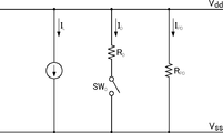
- FIG. 2 shows a circuit model of the device under test 200 in consideration of defects.
- a stationary current IDDQ flows between the power supply voltage Vdd of the power supply terminal and the ground potential Vss. Note that Vss does not need to be a ground potential.
- Vss does not need to be a ground potential.
- the pattern-dependent defect may refer to a defect due to a so-called bridge failure.
- a bridge failure is a failure in which internal wiring in a circuit is short-circuited with a certain resistance value. When there is no bridge failure, the resistance value can be regarded as infinite. When such a bridge fault exists, an abnormal current determined by the power supply voltage and the resistance value flows between the internal wirings according to the logic state of the logic circuit connected to the internal wiring.
- one NAND circuit when two internal wirings are respectively connected to the output ends of the NAND circuit, one NAND circuit outputs a logical value 1 and the other NAND circuit outputs a logical value 0, two internal wirings A current corresponding to the bridge resistance value flows between them. Also, in a state where both NAND circuits output a logical value 0, no abnormal current flows between the two internal wirings.
- the logic state of each logic circuit is determined by the pattern input to the device under test 200, and an abnormal power supply current corresponding to the pattern flows.
- the abnormal power supply current changes in proportion to the power supply voltage according to the bridge resistance value when the power supply voltage is changed.
- the passive defect may refer to a defect that acts like a resistor due to a failure of the CMOS itself. Even in this case, an abnormal power supply current proportional to the power supply voltage flows through the device under test 200.
- normal current I L is constant current flows not generally depend on Vdd.
- Normal current I L as but miniaturization is described later progress also changes depending on the power supply voltage Vdd.
- the pattern-dependent defect current ID varies depending on the state of the switch SW D that is the pattern state, a current proportional to Vdd flows if the pattern state does not change. Therefore, the pattern-dependent defect current ID can be expressed by a circuit having the resistance RD . Since the passive defect current I PD also flows a current proportional to Vdd represented by a resistor circuit having a resistance R PD.
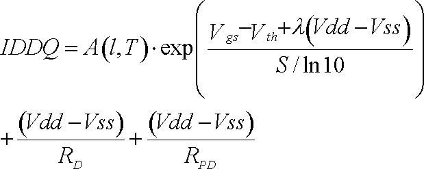
- Equation 1 may be an example of a stationary current equation.
- the first term on the right side (corresponding to the current first term described above) is the normal current IL
- the second term and the third term (corresponding to the current second term described above) are the pattern dependent defect current I. D and passive defect current IPD .
- a (l, T) is a parameter depending on the pattern l and the temperature T
- Vgs is a gate-source voltage
- Vth is a threshold voltage of the MOSFET.
- ⁇ indicates a barrier lowering effect (Drain-Induced-Barrier Lowering: DIBL) due to an increase in the drain voltage (Vdd), and indicates the Vdd dependence of the threshold voltage Vth .
- S is a subthreshold slope and is shown in Equation 2.
- Equation 2 k is the Boltzmann constant
- T denotes the temperature
- q is the unit charge
- C D is the depletion layer capacitance
- C OX oxide capacitance.
- normal current I L does not depend on Vdd.
- the normal current IL is a constant current source.
- lambda is now have significant value, can not be ignored Vdd dependence of the normal current I L.
- Defect or pattern dependent defect current I D and the passive defect current I PD due to failure also because it has a Vdd dependence simply measures the IDDQ by changing the Vdd can not be separated normal current and an abnormal current.
- the normal current I L may vary depending on the Vdd, Vdd to changes exponentially as shown in Equation 1.
- Equation 1 since the stationary current IDDQ shown in Equation 1 includes both normal current and abnormal current, it is necessary to separate the normal current from the abnormal current, but since both have Vdd dependency, they are simply separated. Can not. However, since the normal current changes exponentially with respect to Vdd, and the abnormal current changes in proportion to Vdd, both can be separated using this. That is, the equation of Equation 1 is modified as shown in Equation 3, and the terms related to the normal current are collected on the right side. Equation 3 may be an example of a stationary current equation. In Equation 3, the resistance R represents a parallel resistance of R D and R PD .
- Equation 4 may be an example of a stationary current equation.
- the power supply control unit 120 is controlled so that the first voltage V1 is output from the power supply unit 110, and the first voltage V1 is applied to the device under test 200.
- the current measurement unit 130 measures the stationary current IDDQ1.
- the output of the power supply unit 110 is changed to the second voltage V2, and the quiescent current IDDQ2 is measured.
- the output of the power supply unit 110 is changed to the third voltage V3, and the stationary current IDDQ3 is measured.
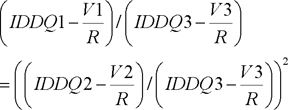
- the value of the resistance R can be obtained by using IDDQ1 corresponding to the first voltage V1, IDDQ2 corresponding to the second voltage V2, IDDQ3 corresponding to the third voltage V3, and Equation 4. That is, the first equation in which IDDQ1 corresponding to the first voltage V1 is substituted into Equation 4, the second equation in which IDDQ2 corresponding to the second voltage V2 is substituted into Equation 4, and the IDDQ3 corresponding to the third voltage V3 is The value of the resistance R can be obtained from the relational expression obtained by computing the third expression assigned to 4 with each other. The value of the resistance R can be obtained by the following procedure, for example.
- Equation 7 may be an example of a relational expression obtained by eliminating the first current term by calculating the first expression, the second expression, and the third expression.
- the value of the resistance R related to the defect can be obtained.
- the device under test 200 can be determined as a non-defective product, and when the resistance R is less than the predetermined value, it can be determined that the device under test 200 is defective.
- the test apparatus 100 of the present embodiment normalization and abnormal current with high accuracy can be achieved even when the miniaturization progresses and a leakage current depending on Vdd occurs even in a normal element.
- the IDDQ test of the device under test 200 can be performed.
- the test coverage can be improved without increasing the test pattern.
Landscapes
- Engineering & Computer Science (AREA)
- General Engineering & Computer Science (AREA)
- Physics & Mathematics (AREA)
- General Physics & Mathematics (AREA)
- Tests Of Electronic Circuits (AREA)
- Testing Of Individual Semiconductor Devices (AREA)
Abstract
Description
出願番号12/209,213 出願日 2008年9月12日


Claims (9)
- 被試験デバイスを試験する試験装置であって、
前記被試験デバイスの電源端子に電力を供給する電源部と、
複数の電圧レベルで前記電源部が前記電力を出力するよう制御する電源制御部と、
前記電源部から前記電源端子に供給される前記被試験デバイスの電源電流であって、前記被試験デバイスに入力される論理パターンが遷移してから所定の時間が経過した時点における静止時電流を、前記複数の電圧レベルごとに測定する電流測定部と、
前記電流測定部が測定した電圧レベルごとの電流値のうち少なくとも3つの電流値を利用して、前記被試験デバイスの欠陥の有無を解析する解析部と、
を備えた試験装置。 - 前記解析部は、
所定の欠陥の無いデバイスに前記静止時電流として流れる正常電流および前記電圧レベルの関係と、所定の欠陥の有るデバイスに前記静止時電流として流れる異常電流および前記電圧レベルの関係とを予め格納し、
前記少なくとも3つの電流値と、前記正常電流および前記電圧レベルの関係と、前記異常電流および前記電圧レベルの関係とに基づいて、前記被試験デバイスの欠陥の有無を解析する
請求項1に記載の試験装置。 - 前記解析部は、前記正常電流および前記電圧レベルの関係として、指数関数で表わされる関係を格納し、前記異常電流および前記電圧レベルの関係として、線形な関係を格納する
請求項2に記載の試験装置。 - 前記解析部は、前記少なくとも3つの電流値と、前記正常電流および前記電圧レベルの関係と、前記異常電流および前記電圧レベルの関係とに基づいて、前記電圧レベルに対して線形に変化する前記静止時電流の線形成分と、前記電圧レベルに対して指数関数的に変化する前記静止時電流の指数成分とを分離し、前記静止時電流の線形成分に基づいて、前記被試験デバイスの欠陥の有無を解析する
請求項3に記載の試験装置。 - 前記解析部は、前記電源端子に供給される静止時電流を表す式であって、印加される電圧に対して指数関数的に値が増加する第1電流項および印加される電圧に比例して値が増加する第2電流項を有する静止時電流式に基づき、前記欠陥に関連する抵抗値を求める、
請求項1に記載の試験装置。 - 前記解析部は、第1電圧レベルに対応する第1電流値を前記静止時電流式に代入した第1式、第2電圧レベルに対応する第2電流値を前記静止時電流式に代入した第2式、および、第3電圧レベルに対応する第3電流値を前記静止時電流式に代入した第3式、を互いに演算することにより前記第1電流項を消去して得た関係式から、前記抵抗値を求める、
請求項5に記載の試験装置。 - 前記被試験デバイスに与えるパターンを生成するパターン生成部をさらに備え、
前記電流測定部は、前記パターン生成部で生成した前記パターンが前記被試験デバイスに加えられている状態で、前記電圧レベルごとの前記静止時電流を測定する、
請求項1に記載の試験装置。 - 前記パターン生成部は、複数のパターンを生成し、
前記電流測定部は、前記複数のパターンごとに前記静止時電流を測定する、
請求項7に記載の試験装置。 - 被試験デバイスを試験する試験方法であって、
前記被試験デバイスの電源端子に第1電圧を印加して、電源部から前記電源端子に供給される前記被試験デバイスの電源電流であって、前記被試験デバイスに入力される論理パターンが遷移してから所定の時間が経過した時点における静止時電流を、前記第1電圧に対応する第1電流値として測定する段階と、
前記被試験デバイスの電源端子に第2電圧を印加して、前記電源端子に供給される前記被試験デバイスの前記静止時電流を、前記第2電圧に対応する第2電流値として測定する段階と、
前記被試験デバイスの電源端子に第3電圧を印加して、前記電源端子に供給される前記被試験デバイスの前記静止時電流を、前記第3電圧に対応する第3電流値として測定する段階と、
前記第1電流値、前記第2電流値および前記第3電流値を利用して、前記被試験デバイスの欠陥の有無を解析する段階と、
を備えた試験方法。
Priority Applications (2)
| Application Number | Priority Date | Filing Date | Title |
|---|---|---|---|
| CN2009801332571A CN102132165B (zh) | 2008-09-12 | 2009-09-11 | 测试装置及测试方法 |
| JP2010528665A JPWO2010029772A1 (ja) | 2008-09-12 | 2009-09-11 | 試験装置および試験方法 |
Applications Claiming Priority (2)
| Application Number | Priority Date | Filing Date | Title |
|---|---|---|---|
| US12/209,213 US7859288B2 (en) | 2008-09-12 | 2008-09-12 | Test apparatus and test method for testing a device based on quiescent current |
| US12/209,213 | 2008-09-12 |
Publications (1)
| Publication Number | Publication Date |
|---|---|
| WO2010029772A1 true WO2010029772A1 (ja) | 2010-03-18 |
Family
ID=42005036
Family Applications (1)
| Application Number | Title | Priority Date | Filing Date |
|---|---|---|---|
| PCT/JP2009/004547 Ceased WO2010029772A1 (ja) | 2008-09-12 | 2009-09-11 | 試験装置および試験方法 |
Country Status (5)
| Country | Link |
|---|---|
| US (1) | US7859288B2 (ja) |
| JP (1) | JPWO2010029772A1 (ja) |
| CN (1) | CN102132165B (ja) |
| TW (1) | TW201013202A (ja) |
| WO (1) | WO2010029772A1 (ja) |
Families Citing this family (3)
| Publication number | Priority date | Publication date | Assignee | Title |
|---|---|---|---|---|
| TWI483104B (zh) * | 2011-12-20 | 2015-05-01 | Hon Hai Prec Ind Co Ltd | 電子裝置測試系統及方法 |
| JP2013181831A (ja) * | 2012-03-01 | 2013-09-12 | Advantest Corp | 試験装置 |
| US10082856B1 (en) * | 2016-09-29 | 2018-09-25 | Juniper Networks, Inc. | Performing a health check on power supply modules that operate in a current sharing mode |
Citations (4)
| Publication number | Priority date | Publication date | Assignee | Title |
|---|---|---|---|---|
| JPH10332775A (ja) * | 1997-06-02 | 1998-12-18 | Nec Corp | 電界効果トランジスタの寄生ソース抵抗評価方法 |
| JP2000171529A (ja) * | 1998-12-01 | 2000-06-23 | Agilent Technol Inc | 回路欠陥検出システム及び回路欠陥検出方法 |
| JP2004219115A (ja) * | 2003-01-09 | 2004-08-05 | Sony Corp | 欠陥検出装置及び方法、並びに欠陥検出プログラム |
| WO2006041064A1 (ja) * | 2004-10-12 | 2006-04-20 | Advantest Corporation | 試験装置、試験方法、電子デバイス、及びデバイス生産方法 |
Family Cites Families (4)
| Publication number | Priority date | Publication date | Assignee | Title |
|---|---|---|---|---|
| JPH06308197A (ja) * | 1993-04-27 | 1994-11-04 | Fujitsu Ltd | Ic素子試験装置 |
| JP2001091568A (ja) * | 1999-09-17 | 2001-04-06 | Advantest Corp | 半導体集積回路の試験装置及び試験方法 |
| JP3696507B2 (ja) * | 2000-12-28 | 2005-09-21 | 株式会社アドバンテスト | 試験装置、試験方法、及び生産方法 |
| JP4630122B2 (ja) | 2005-05-11 | 2011-02-09 | 株式会社アドバンテスト | 試験装置、及び試験方法 |
-
2008
- 2008-09-12 US US12/209,213 patent/US7859288B2/en active Active
-
2009
- 2009-09-11 CN CN2009801332571A patent/CN102132165B/zh active Active
- 2009-09-11 JP JP2010528665A patent/JPWO2010029772A1/ja not_active Ceased
- 2009-09-11 TW TW098130793A patent/TW201013202A/zh unknown
- 2009-09-11 WO PCT/JP2009/004547 patent/WO2010029772A1/ja not_active Ceased
Patent Citations (4)
| Publication number | Priority date | Publication date | Assignee | Title |
|---|---|---|---|---|
| JPH10332775A (ja) * | 1997-06-02 | 1998-12-18 | Nec Corp | 電界効果トランジスタの寄生ソース抵抗評価方法 |
| JP2000171529A (ja) * | 1998-12-01 | 2000-06-23 | Agilent Technol Inc | 回路欠陥検出システム及び回路欠陥検出方法 |
| JP2004219115A (ja) * | 2003-01-09 | 2004-08-05 | Sony Corp | 欠陥検出装置及び方法、並びに欠陥検出プログラム |
| WO2006041064A1 (ja) * | 2004-10-12 | 2006-04-20 | Advantest Corporation | 試験装置、試験方法、電子デバイス、及びデバイス生産方法 |
Also Published As
| Publication number | Publication date |
|---|---|
| US7859288B2 (en) | 2010-12-28 |
| CN102132165B (zh) | 2013-07-03 |
| TW201013202A (en) | 2010-04-01 |
| CN102132165A (zh) | 2011-07-20 |
| JPWO2010029772A1 (ja) | 2012-02-02 |
| US20100066403A1 (en) | 2010-03-18 |
Similar Documents
| Publication | Publication Date | Title |
|---|---|---|
| US10481204B2 (en) | Methods and systems to measure a signal on an integrated circuit die | |
| US20200072897A1 (en) | Optimization of integrated circuit reliability | |
| TWI392887B (zh) | 測試裝置、測試方法以及記錄媒體 | |
| Biswas et al. | An industrial study of system-level test | |
| JPWO2010029772A1 (ja) | 試験装置および試験方法 | |
| US7283918B2 (en) | Apparatus for analyzing fault of semiconductor integrated circuit, method for the same, and computer readable medium for the same | |
| US7539589B2 (en) | Testing radio frequency and analogue circuits | |
| TWI384241B (zh) | 測量設備、測試系統以及測量方法 | |
| JP2001249161A (ja) | 集積回路試験方法 | |
| WO2018026696A1 (en) | Activity coverage assessment of circuit designs under test stimuli | |
| Devarakond et al. | Concurrent device/specification cause–effect monitoring for yield diagnosis using alternate diagnostic signatures | |
| US20170220706A1 (en) | Systems, methods and apparatus that employ statistical analysis of structural test information to identify yield loss mechanisms | |
| US20100079163A1 (en) | Measurement equipment, test system, and measurement method | |
| JP2006119101A (ja) | 半導体試験装置及び半導体集積回路の試験方法 | |
| JPWO2008069025A1 (ja) | 半導体装置 | |
| JP3372488B2 (ja) | 半導体cmos集積回路の試験装置 | |
| Tenentes et al. | Leakage current analysis for diagnosis of bridge defects in power-gating designs | |
| Kundu et al. | On detection of resistive bridging defects by low-temperature and low-voltage testing | |
| JP2004257815A (ja) | 半導体集積回路の検査方法および半導体集積回路装置 | |
| Suenaga et al. | Built-in IDDT appearance time sensor for detecting open faults in 3D IC | |
| Wen et al. | Functional OBIRCH strategy in analyzing complex functional failures including logic failures | |
| Nakanishi et al. | A BIC sensor capable of adjusting IDDQ limit in tests | |
| CN113030712A (zh) | 电路检查方法及电子设备 | |
| TW202124983A (zh) | 電路檢查方法及電子設備 | |
| Kaltchenko et al. | Temperature dependence of I DDQ distribution: application for thermal delta I DDQ testing |
Legal Events
| Date | Code | Title | Description |
|---|---|---|---|
| WWE | Wipo information: entry into national phase |
Ref document number: 200980133257.1 Country of ref document: CN |
|
| 121 | Ep: the epo has been informed by wipo that ep was designated in this application |
Ref document number: 09812921 Country of ref document: EP Kind code of ref document: A1 |
|
| WWE | Wipo information: entry into national phase |
Ref document number: 2010528665 Country of ref document: JP |
|
| NENP | Non-entry into the national phase |
Ref country code: DE |
|
| 122 | Ep: pct application non-entry in european phase |
Ref document number: 09812921 Country of ref document: EP Kind code of ref document: A1 |