WO2010029634A1 - 抵抗変化素子及び情報記録再生装置 - Google Patents
抵抗変化素子及び情報記録再生装置 Download PDFInfo
- Publication number
- WO2010029634A1 WO2010029634A1 PCT/JP2008/066471 JP2008066471W WO2010029634A1 WO 2010029634 A1 WO2010029634 A1 WO 2010029634A1 JP 2008066471 W JP2008066471 W JP 2008066471W WO 2010029634 A1 WO2010029634 A1 WO 2010029634A1
- Authority
- WO
- WIPO (PCT)
- Prior art keywords
- layer
- resistance change
- resistance
- variable resistance
- voltage
- Prior art date
- Legal status (The legal status is an assumption and is not a legal conclusion. Google has not performed a legal analysis and makes no representation as to the accuracy of the status listed.)
- Ceased
Links
Images



















Classifications
-
- G—PHYSICS
- G11—INFORMATION STORAGE
- G11B—INFORMATION STORAGE BASED ON RELATIVE MOVEMENT BETWEEN RECORD CARRIER AND TRANSDUCER
- G11B9/00—Recording or reproducing using a method not covered by one of the main groups G11B3/00 - G11B7/00; Record carriers therefor
- G11B9/04—Recording or reproducing using a method not covered by one of the main groups G11B3/00 - G11B7/00; Record carriers therefor using record carriers having variable electric resistance; Record carriers therefor
-
- B—PERFORMING OPERATIONS; TRANSPORTING
- B82—NANOTECHNOLOGY
- B82Y—SPECIFIC USES OR APPLICATIONS OF NANOSTRUCTURES; MEASUREMENT OR ANALYSIS OF NANOSTRUCTURES; MANUFACTURE OR TREATMENT OF NANOSTRUCTURES
- B82Y10/00—Nanotechnology for information processing, storage or transmission, e.g. quantum computing or single electron logic
-
- G—PHYSICS
- G11—INFORMATION STORAGE
- G11C—STATIC STORES
- G11C11/00—Digital stores characterised by the use of particular electric or magnetic storage elements; Storage elements therefor
- G11C11/56—Digital stores characterised by the use of particular electric or magnetic storage elements; Storage elements therefor using storage elements with more than two stable states represented by steps, e.g. of voltage, current, phase, frequency
-
- G—PHYSICS
- G11—INFORMATION STORAGE
- G11C—STATIC STORES
- G11C13/00—Digital stores characterised by the use of storage elements not covered by groups G11C11/00, G11C23/00, or G11C25/00
- G11C13/0002—Digital stores characterised by the use of storage elements not covered by groups G11C11/00, G11C23/00, or G11C25/00 using resistive RAM [RRAM] elements
- G11C13/0021—Auxiliary circuits
- G11C13/003—Cell access
-
- G—PHYSICS
- G11—INFORMATION STORAGE
- G11C—STATIC STORES
- G11C16/00—Erasable programmable read-only memories
- G11C16/02—Erasable programmable read-only memories electrically programmable
- G11C16/04—Erasable programmable read-only memories electrically programmable using variable threshold transistors, e.g. FAMOS
- G11C16/0483—Erasable programmable read-only memories electrically programmable using variable threshold transistors, e.g. FAMOS comprising cells having several storage transistors connected in series
-
- H—ELECTRICITY
- H10—SEMICONDUCTOR DEVICES; ELECTRIC SOLID-STATE DEVICES NOT OTHERWISE PROVIDED FOR
- H10B—ELECTRONIC MEMORY DEVICES
- H10B63/00—Resistance change memory devices, e.g. resistive RAM [ReRAM] devices
-
- H—ELECTRICITY
- H10—SEMICONDUCTOR DEVICES; ELECTRIC SOLID-STATE DEVICES NOT OTHERWISE PROVIDED FOR
- H10N—ELECTRIC SOLID-STATE DEVICES NOT OTHERWISE PROVIDED FOR
- H10N70/00—Solid-state devices having no potential barriers, and specially adapted for rectifying, amplifying, oscillating or switching
- H10N70/20—Multistable switching devices, e.g. memristors
-
- H—ELECTRICITY
- H10—SEMICONDUCTOR DEVICES; ELECTRIC SOLID-STATE DEVICES NOT OTHERWISE PROVIDED FOR
- H10N—ELECTRIC SOLID-STATE DEVICES NOT OTHERWISE PROVIDED FOR
- H10N70/00—Solid-state devices having no potential barriers, and specially adapted for rectifying, amplifying, oscillating or switching
- H10N70/801—Constructional details of multistable switching devices
- H10N70/881—Switching materials
- H10N70/883—Oxides or nitrides
-
- G—PHYSICS
- G11—INFORMATION STORAGE
- G11C—STATIC STORES
- G11C2211/00—Indexing scheme relating to digital stores characterized by the use of particular electric or magnetic storage elements; Storage elements therefor
- G11C2211/56—Indexing scheme relating to G11C11/56 and sub-groups for features not covered by these groups
- G11C2211/564—Miscellaneous aspects
- G11C2211/565—Multilevel memory comprising elements in triple well structure
-
- G—PHYSICS
- G11—INFORMATION STORAGE
- G11C—STATIC STORES
- G11C2213/00—Indexing scheme relating to G11C13/00 for features not covered by this group
- G11C2213/10—Resistive cells; Technology aspects
- G11C2213/17—Memory cell being a nanowire transistor
-
- G—PHYSICS
- G11—INFORMATION STORAGE
- G11C—STATIC STORES
- G11C2213/00—Indexing scheme relating to G11C13/00 for features not covered by this group
- G11C2213/30—Resistive cell, memory material aspects
- G11C2213/35—Material including carbon, e.g. graphite, grapheme
-
- G—PHYSICS
- G11—INFORMATION STORAGE
- G11C—STATIC STORES
- G11C2213/00—Indexing scheme relating to G11C13/00 for features not covered by this group
- G11C2213/50—Resistive cell structure aspects
- G11C2213/56—Structure including two electrodes, a memory active layer and a so called passive or source or reservoir layer which is NOT an electrode, wherein the passive or source or reservoir layer is a source of ions which migrate afterwards in the memory active layer to be only trapped there, to form conductive filaments there or to react with the material of the memory active layer in redox way
-
- G—PHYSICS
- G11—INFORMATION STORAGE
- G11C—STATIC STORES
- G11C2213/00—Indexing scheme relating to G11C13/00 for features not covered by this group
- G11C2213/70—Resistive array aspects
- G11C2213/71—Three dimensional array
-
- G—PHYSICS
- G11—INFORMATION STORAGE
- G11C—STATIC STORES
- G11C2213/00—Indexing scheme relating to G11C13/00 for features not covered by this group
- G11C2213/70—Resistive array aspects
- G11C2213/72—Array wherein the access device being a diode
-
- G—PHYSICS
- G11—INFORMATION STORAGE
- G11C—STATIC STORES
- G11C2213/00—Indexing scheme relating to G11C13/00 for features not covered by this group
- G11C2213/70—Resistive array aspects
- G11C2213/75—Array having a NAND structure comprising, for example, memory cells in series or memory elements in series, a memory element being a memory cell in parallel with an access transistor
-
- G—PHYSICS
- G11—INFORMATION STORAGE
- G11C—STATIC STORES
- G11C2213/00—Indexing scheme relating to G11C13/00 for features not covered by this group
- G11C2213/70—Resistive array aspects
- G11C2213/79—Array wherein the access device being a transistor
Definitions
- the present invention relates to a resistance change element and an information recording / reproducing apparatus.
- NAND flash memory and small HDD hard disk drive
- Non-Patent Documents 1 and 2 a memory using a resistance change material having a low resistance state and a high resistance state has been proposed (for example, Non-Patent Documents 1 and 2).
- a voltage pulse can be applied to the variable resistance material to repeatedly change between a low resistance state and a high resistance state, and these two states correspond to binary data “0” and “1”.
- To record data a memory using a resistance change material having a low resistance state and a high resistance state.
- Such an information recording / reproducing apparatus is expected to enable multi-value recording and further increase the recording density.
- P Bachtold G. Cherubini, C. Hagleitner, T. Loeliger, A. Pantazi, H. Pozidis and E. Eleftheriou, in Technical Digest, IEDM03 pp.763-766
- variable resistance element and an information recording / reproducing apparatus capable of multi-value recording are provided.
- a first resistance change layer that exhibits a plurality of states having different electrical resistivity depending on at least one of an applied voltage and an energized current is stacked on the first resistance change layer.
- a second variable resistance layer having a composition different from that of the first variable resistance layer and exhibiting a plurality of states having different electrical resistivity depending on at least one of an applied voltage and an applied current.
- a variable resistance portion; and an electrode layer that performs at least one of voltage application and current flow perpendicular to the film surface of the variable resistance portion, and includes a plurality of different states in the first variable resistance layer. At least one of the transition voltage and current and at least one of the transition voltage and current between the plurality of different states in the second resistance change layer are different from each other.
- the variable resistance element is provided, wherein.
- an information recording / reproducing apparatus comprising: a drive unit that records information by causing the resistance change unit to transition between a plurality of resistance states.
- 1 is a schematic cross-sectional view illustrating the configuration of a resistance change element according to a first embodiment of the invention. It is a schematic diagram which illustrates the structure of the principal part of the information recording / reproducing apparatus to which the variable resistance element according to the first embodiment of the present invention is applied. It is a schematic diagram which illustrates the characteristic of the variable resistance element which concerns on the 1st Embodiment of this invention. It is a schematic diagram which illustrates the characteristic of the variable resistance element which concerns on the 1st Embodiment of this invention. It is another graph which illustrates the characteristic of the resistance change element concerning a 1st embodiment of the present invention. It is another schematic diagram which illustrates the characteristic of the variable resistance element which concerns on the 1st Embodiment of this invention.
- FIG. 5 is a schematic cross-sectional view illustrating the configuration of a resistance change element according to a second embodiment of the invention.
- FIG. 6 is a schematic cross-sectional view illustrating the configuration of a resistance change element according to a third embodiment of the invention. It is a typical sectional view which illustrates the composition of another variable resistance element concerning a 3rd embodiment of the present invention.
- FIG. 9 is a schematic cross-sectional view illustrating the configuration of a resistance change element according to a fourth embodiment of the invention.
- FIG. 10 is a schematic cross-sectional view illustrating the configuration of another resistance change element according to the fourth embodiment of the invention.
- FIG. 9 is a schematic cross-sectional view illustrating the configuration of a resistance change element according to a fifth embodiment of the invention.
- FIG. 10 is a schematic cross-sectional view illustrating the configuration of another variable resistance element according to the fifth embodiment of the invention. It is a typical sectional view which illustrates the composition of the resistance change element concerning a 6th embodiment of the present invention.
- FIG. 10 is a schematic cross-sectional view illustrating the configuration of a resistance change element according to a seventh embodiment of the invention. It is a schematic diagram illustrating the configuration and operation of a part of the resistance change element according to the embodiment of the invention. It is a typical sectional view which illustrates a part of composition and operation of a variable resistance element concerning an embodiment of the present invention.
- FIG. 1 is a schematic cross-sectional view illustrating the configuration of a resistance change element according to an embodiment of the invention. It is a typical perspective view which illustrates the structure of the information recording / reproducing apparatus which concerns on the 8th Embodiment of this invention.
- FIG. 20 is a schematic plan view illustrating the configuration of a part of an information recording / reproducing apparatus according to an eighth embodiment of the invention. It is a schematic diagram which illustrates operation
- FIG. 1 It is a schematic diagram which illustrates reproduction
- FIG. 25 is a schematic perspective view illustrating the configuration of another information recording / reproducing apparatus according to the ninth embodiment of the invention.
- FIG. 25 is a schematic perspective view illustrating the configuration of another information recording / reproducing apparatus according to the ninth embodiment of the invention. It is a typical sectional view which illustrates the composition of the principal part of the information recording / reproducing apparatus concerning a 10th embodiment of the present invention.
- FIG. 20 is a schematic cross-sectional view illustrating the operation of an information recording / reproducing apparatus according to a tenth embodiment of the invention. It is a schematic diagram which illustrates the structure of the principal part of another information recording / reproducing apparatus which concerns on the 10th Embodiment of this invention.
- FIG. 10 It is a schematic diagram which illustrates the structure of the principal part of another information recording / reproducing apparatus which concerns on the 10th Embodiment of this invention. It is a typical sectional view which illustrates the principal part of another information recording and reproducing device concerning a 10th embodiment of the present invention. It is a typical sectional view which illustrates the principal part of the information recording / reproducing apparatus of the modification concerning the 10th embodiment of the present invention.
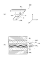
- FIG. 1 is a schematic cross-sectional view illustrating the configuration of a variable resistance element according to the first embodiment of the invention.
- the resistance change element 310 according to the first embodiment of the present invention includes a first resistance change layer (first memory layer) 12 ⁇ / b> A ⁇ b> 1, a second resistance change layer ( (Second recording layer) 12A2 and upper electrode 13A are sequentially stacked. That is, the resistance change portion (recording portion) 12 includes a first recording layer 12A1 and a second resistance change layer 12A2.
- the nonvolatile memory element 310 can be applied to, for example, a nonvolatile memory such as a cross point type, a probe memory type, and various flash memory types.
- a configuration of the nonvolatile memory element 310 when the nonvolatile memory element 310 is used in a cross-point nonvolatile memory device will be described.
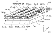
- FIG. 2 is a schematic view illustrating the configuration of the main part of an information recording / reproducing apparatus to which the variable resistance element according to the first embodiment of the invention is applied.
- the memory cell 33 and the rectifying element 34 are used in the cross-point type information recording / reproducing apparatus 210. Is provided.
- the upper and lower arrangement relationship between the word line WL i and the bit line BL j is arbitrary.
- the arrangement relationship between the memory cell 33 and the rectifying element 34 between the word line WL i and the bit line BL j is also arbitrary. That is, in the specific example illustrated in FIG. 2, the memory cell 33 is disposed on the bit line BL j side with respect to the rectifying element 34, but the memory cell 33 is disposed on the word line WL i side with respect to the rectifying element 34. May be.
- the memory cell 33 includes a resistance change element 310.
- the resistance change element 310 includes a lower electrode 11, an upper electrode 13A, and a recording layer 12 provided between the lower electrode 11 and the upper electrode 13A.
- the upper electrode 13A and the lower electrode 11 are convenient names and can be interchanged.
- the memory cell 33 can include a protective layer 33B and a heater layer 35 provided between the resistance change element 310 and the protection layer 33B.
- the protective layer 33B is provided on the bit line BL j side of the variable resistance element 310, but the protective layer 33B may be provided on the word line WL i side of the variable resistance element 310. Alternatively, it may be provided between the rectifying element 34 and the word line WL i .
- the heater layer 35 and the protective layer 33B are provided as necessary and can be omitted.
- a plurality of these word lines WL i , rectifying elements 34, memory cells 33, and bit lines BL j are provided, and an insulating layer is provided between them to be insulated from each other.
- At least one of the lower electrode 11 and the upper electrode 13A of the resistance change element 310 is adjacent to the resistance change element 310, for example, the word line WL i , the rectifier element 34, the heater layer 35, the protective layer 33B, and the bit line BL j. It may be combined with at least one of the above. In this case, a layer that is also used as at least one of the lower electrode 11 and the upper electrode 13A is regarded as at least one of the lower electrode 11 and the upper electrode 13A.
- either the lower electrode 11 or the upper electrode 13A can be omitted depending on the application to which the variable resistance element 310 is applied. Below, in order to demonstrate easily, it demonstrates as a case where both the lower electrode 11 and the upper electrode 13A are provided.
- the lower electrode 11 and the upper electrode 13A have convenient names and can be interchanged. Further, in the positional relationship between the lower electrode 11 and the upper electrode 13A, the first variable resistance layer 12A1 and the second resistance change layer 12A2 can be interchanged with each other.
- Each of the first resistance change layer 12A1 and the second resistance change layer 12A2 is a layer whose resistance changes, that is, a resistance change layer. That is, the resistance of the first resistance change layer 12A1 changes depending on at least one of the voltage applied to the first resistance change layer 12A1 and the current passed through the first resistance change layer 12A1.
- the resistance of the second resistance change layer 12A2 changes depending on at least one of a voltage applied to the second resistance change layer 12A2 and a current passed through the second resistance change layer 12A2.
- the first variable resistance layer 12A1 and the second variable resistance layer 12A2 have different electrical characteristics. That is, at least one of the voltage and current at which the resistance changes in the first resistance change layer 12A1, and at least one of the voltage and current at which the resistance changes in the second resistance change layer 12A2 are different from each other.
- the difference in characteristics can be changed depending on the material and thickness used for the first resistance change layer 12A1 and the second resistance change layer 12A2.
- FIG. 3 is a schematic view illustrating characteristics of the variable resistance element according to the first embodiment of the invention. That is, this figure is a schematic graph illustrating the current-voltage characteristics of the variable resistance element 310 according to this embodiment, and the horizontal axis represents the current flowing between the lower electrode 11 and the upper electrode 13A, that is, the resistance.
- the current I flowing through the changing unit 12 and the vertical axis represents the voltage applied to the lower electrode 11 and the upper electrode 13 ⁇ / b> A, that is, the voltage V applied to the resistance changing unit 12.
- the resistance change element 310 has, for example, five different regions, that is, regions R1 to R5 in the current-voltage characteristics.
- the region R1 is, for example, a region where both the first resistance change layer 12A1 and the second resistance change layer 12A2 are in a high resistance state.
- the region R2 is, for example, a region where the first resistance change layer 12A1 is in a low resistance state and the second resistance change layer 12A2 is in a high resistance state.
- the region R3 is, for example, a region where the first resistance change layer 12A1 and the second resistance change layer 12A2 are in a low resistance state.
- the region R4 is a region in which the first resistance change layer 12A1 is again in the high resistance state (reset state) and the second resistance change layer 12A2 is in the low resistance state.
- the region R5 is a region where both the first resistance change layer 12A1 and the second resistance change layer 12A2 are again in the high resistance state (reset state).
- the recording unit 12 By stacking the first variable resistance layer 12A1 and the second variable resistance layer 12A2 having different characteristics as described above, the recording unit 12 exhibits three or more different resistance states, that is, three or more values. Can do.
- the resistance change element 310 according to the present embodiment, a resistance change element capable of multi-value recording is provided.
- the resistance change unit 12 includes two resistance change layers (the first resistance change layer 12A1 and the second resistance change layer 12A2). It may have a layer.
- the recording unit 12 When not using the reset state, the recording unit 12 has two resistance change layers, and when there is no intermediate state in the resistance change state, two levels of information per resistance change layer. Are recorded, it is possible to record and reproduce a total of four levels of 2 levels ⁇ 2 levels. On the other hand, if the above-described reset state is used, at least 3 levels ⁇ 3 levels of 9 levels in total can be recorded and reproduced. If a material having an intermediate state in the resistance change state of the resistance change layer is used, the amount of information that can be recorded can be further increased.
- FIG. 4 is a schematic view illustrating characteristics of the variable resistance element according to the first embodiment of the invention.
- this figure is a schematic graph illustrating the characteristics of the resistance change layer (each of the first resistance change layer 12A1 and the second resistance change layer 12A2).
- 2A illustrates the current-voltage characteristics of the resistance change layer
- FIG. 2B illustrates the current-resistance characteristics of the resistance change layer.
- the resistance change layer has a relatively high resistance state (high resistance state HR) and a relatively low resistance state according to applied current and voltage ( It exhibits two states, a low resistance state LR).
- high resistance state HR high resistance state
- low resistance state LR low resistance state LR
- the initial state it is in a high resistance state HR, and when a current or voltage to be applied is increased, at a certain point (hereinafter referred to as a set point), a low resistance state LR (hereinafter referred to as a set state) is obtained.
- a reset point the state returns to the high resistance state HR (hereinafter referred to as a reset state).
- the high resistance state HR is described as a reset state
- the low resistance state LR is described as a reset state.
- this definition is intended to simplify the following description. Depending on the selection of materials and the manufacturing method, this definition may be reversed, that is, the low resistance state LR becomes the reset (initial) state, and the high
- the resistance state HR can also be defined as a set state.
- the current and voltage at the set point are referred to as set current Is and set voltage Vs, respectively, and the current and voltage at the reset point are referred to as reset current Ir and reset voltage Vr, respectively.
- the resistance value in the set state is referred to as a set resistor Rs, and the resistance value in the reset state is referred to as a reset resistor Rr.
- the set current Is, the set voltage Vs, the reset current Ir, the reset voltage Vr, the set resistance Rs, and the reset resistance Rr of the resistance change layer differ depending on the material, cross-sectional area, film thickness, and the like of the resistance change element used as the resistance change layer.
- variable resistance element when using the variable resistance element according to the present embodiment, a bipolar operation is also possible in which a reset state is applied by applying a voltage having a polarity opposite to the set voltage Vs.
- the description is limited to the unipolar operation in which the polarity of the applied current or voltage is constant, and the current or voltage represents an absolute value.
- the resistance change layer becomes low.
- the resistance value state LR is maintained in the set state.
- the resistance change layer Holds the reset state of the high resistance value state HR. Furthermore, by setting the current and voltage applied to the resistance change layer to be lower than the set current Is and the set voltage Vs, the resistance of the resistance layer can be detected without changing the state of the resistance change layer. Can be read.
- the resistance change layer can perform writing by setting the applied current and voltage to be equal to or higher than the set current Is and the set voltage Vs and lower than the reset current Ir and the reset voltage Vr.
- the erasing can be performed by setting the current and voltage to the reset current Ir and the reset voltage Vr or higher.
- the applied current and voltage by setting the applied current and voltage to be less than the set current Is and the set voltage Vs, it functions as a nonvolatile memory cell that can read the state as a resistor.
- the first resistance change layer 12A1 and the second resistance change layer 12A2 each function as a 1-bit memory cell.
- the amount of information that can be recorded can be further increased. Note that writing and erasing can also be performed by current pulses or voltage pulses.
- the resistance change unit 12 of the resistance change element 310 has a structure in which the first resistance change layer 12A1 and the second resistance change layer 12A2 that perform such operations are stacked.
- At least one of the set current Is, the set voltage Vs, the reset current Ir, and the reset voltage Vr is different.
- FIG. 5 is another graph illustrating the characteristics of the variable resistance element according to the first embodiment of the invention. That is, FIG. 5A illustrates the current-voltage characteristics of the first resistance change layer 12A1, the second resistance change layer 12A2, and the resistance change unit 12, and FIG. The current-voltage characteristics of the layer 12A1, the second resistance change layer 12A2, and the resistance change unit 12 are illustrated.
- the solid line corresponds to the recording unit 12
- the alternate long and short dash line corresponds to the first resistance change layer 12A1
- the broken line corresponds to the second resistance change layer 12A2.
- the characteristics of these variable resistance layers are approximated linearly and conceptually illustrated.
- subscript 1 is attached to the characteristics of the first variable resistance layer 12A1 single layer
- subscript 2 is attached to the characteristics of the second variable resistance layer 12A2 single layer. These characteristics are shown without subscripts.
- both the first resistance change layer 12A1 and the second resistance change layer 12A2 are in a reset state. Now, increasing the current I to be applied to the recording unit 12, a set current Is 1 of the first variable resistance layer 12A1, the first variable resistance layer 12A1 is changed to the set state. At this time, the first resistance change layer 12A2 remains in the reset state and does not change.
- the second variable resistance layer 12A2 With further increasing the current, the set current Is 2 of the second variable resistance layer 12A2, the second variable resistance layer 12A2 is changed to the set state. At this time, the first resistance change layer 12A1 remains unchanged in the set state.
- the first resistance variable layer 12A1 in the reset current Ir 1 of the first variable resistance layer 12A1 is changed to the reset state.
- the second resistance change layer 12A2 remains in the set state and does not change.
- the reset current Ir 2 of the second variable resistance layer 12A2 With further increasing the current, the reset current Ir 2 of the second variable resistance layer 12A2, the second variable resistance layer 12A2, changes to the reset state. At this time, the first resistance change layer 12A1 remains unchanged in the reset state.
- the resistance change unit 12 takes four states corresponding to four combinations of the set state and the reset state of the first resistance change layer 12A1 and the second resistance change layer 12A2 by the increase of the current I to be energized.
- the resistance change portion 12 by energizing the lower current I than Is 1, can be read without resistance changing the respective states of the first variable resistance layer 12A1 and the second variable resistance layer 12A2. Therefore, the resistance change unit 12 functions as a non-volatile memory cell having four values.
- the resistance change unit 12 including the first resistance change layer 12A1 and the second resistance change layer 12A2 is changed to the first resistance change layer.
- the state of 12A1 is the least significant bit (LSB) and the state of the second resistance change layer 12A2 is the most significant bit (MSB)
- MSB most significant bit
- the state has 2 states “0”, “1”, “2”, “3”. It functions as a bit memory cell.
- the amount of information that can be recorded can be further increased.
- the first resistance change layer 12 ⁇ / b> A ⁇ b> 1 and the second resistance change layer 12 ⁇ / b> A ⁇ b> 2 are each subjected to a voltage proportionally distributed to the respective resistances.
- the voltage at which the state changes is different from the set voltage and the reset voltage of the first resistance change layer 12A1 and the second resistance change layer 12A2 illustrated in FIG.
- the resistance value changes in the current-voltage characteristics of the recording unit 12 as illustrated in FIG. There are four voltage values.
- the voltage transition between each other different states of the first variable resistance layer 12A1 includes a set voltage Vs 1 and the reset voltage Vr 1 above.
- the voltage transition between each other different states in the second variable resistance layer 12A2 includes a set voltage Vs 2 and the reset voltage Vr 2 above.
- the set voltage Vs 1 and the reset voltage Vr 1 are different from the set voltage Vs 2 and the reset voltage Vr 2 .
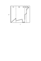
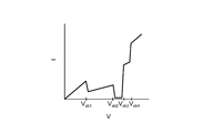
- FIG. 6 is another schematic view illustrating the characteristics of the variable resistance element according to the first embodiment of the invention. That is, this figure illustrates the current-voltage characteristics of the variable resistance element according to the present embodiment, the horizontal axis is the voltage applied to the resistance change unit 12, and the vertical axis is the current flowing through the resistance change unit 12. Indicates. In this figure, the initial state and the reset state are illustrated as a low resistance state, and the set state is illustrated as a high resistance state.
- each voltage at which the resistance of the resistance change unit 12 changes is set as a threshold voltage Vsh, and the first threshold voltage Vsh 1 , the second threshold voltage Vsh 2 ,.
- the Mth threshold voltage is Vsh M.
- V ⁇ Vsh 1 state is held or read.
- Vsh 1 ⁇ V ⁇ Vsh 2
- state is “1”.
- Vsh 2 ⁇ V ⁇ Vsh 3
- Vsh 3 state “2”
- Vsh 3 ⁇ V ⁇ Vsh 4
- Vsh 4 state “3”
- writing, erasing, and reading can be performed by either a current pulse or a voltage pulse.
- the first resistance change layer 12A1 and the second resistance change layer 12A2 are applied only to the first variable resistance layer 12A2.
- the second resistance change layer 12A2 also changes from the high resistance state HR to the low resistance state LR at the same time. If you happen to occur.
- the voltage of the second resistance change layer 12A2 is preferably lower than the voltage at which the second resistance change layer 12A2 shifts from the high resistance state HR to the low resistance state LR.
- the high resistance state HR and the low resistance state LR of each of the first and second resistance change layers 12A1 and 12A2 are used. It can be performed by applying a voltage higher than the voltage that shifts to the first and second resistance change layers 12A1 and 12A2. Actually, it is only necessary to apply the total voltage of the voltage that shifts from the high resistance state HR to the low resistance state LR of each of the first and second resistance change layers 12A1 and 12A2, and this operation can be performed collectively. it can.
- the set voltage and reset voltage (Vs 1 , Vr 1 ) of the first resistance change layer 12A1 and the set voltage and reset voltage (Vs 2 , Vr 2 ) of the second resistance change layer 12A2 are mainly changed in resistance.
- the slope of the current-voltage characteristic in the first resistance change layer 12A1 and the second resistance change layer 12A2, that is, the electrical resistance between on and off, is the layer thickness in the first resistance change layer 12A1 and the second resistance change layer 12A2.
- it is determined by the film thickness and the area perpendicular to the direction of current flow in these layers. Therefore, by controlling the layer thickness of the first resistance change layer 12A and the second resistance change layer and the area perpendicular to the stacking direction, a plurality of resistances (Rs 1 , Rr) of the first resistance change layer 12A1 are controlled. 1 ) and a plurality of resistances (Rs 2 , Rr 2 ) of the second resistance change layer 12A2 can be set to desired values.
- variable resistance element 310 since the variable resistance element 310 has a plurality of variable resistance layers, the electrical resistance as the variable resistance element 310 should be higher than when one variable resistance layer is used. Can do. If the resistance is high and the same voltage is applied, the current value can be kept low. Therefore, the variable resistance element 310 according to the present embodiment leads to low power consumption of an information recording / reproducing apparatus using the variable resistance element 310. As described above, the variable resistance element according to the present embodiment can perform multi-value recording, and at the same time, can reduce power consumption of an information recording / reproducing apparatus using the resistance change element.
- the resistance change unit 12 includes a plurality of resistance change layers (for example, the first resistance change layer 12A1 and the second resistance change layer 12A2) having different compositions.
- the threshold voltages are the set voltage and reset voltage of the respective resistance change layers. This is because at least one of them is different.
- each of the first to fourth threshold voltages Vsh 1 to Vsh 4 illustrated in FIG. 6 includes the set voltage Vs 1 and the reset voltage Vr 1 of the first resistance change layer 12A1 illustrated in FIG. Although the set voltage Vs 2 and the reset voltage Vr 2 of the two-resistance change layer 12A2 do not coincide with each other, the set voltage Vs 1 and the reset voltage Vr 1 , and the set voltage Vs 2 and the reset voltage Vr 2 are different from each other. Is done.
- a resistance change element capable of multi-value recording can be provided.
- the example is described in which the set voltage Vs 1 and reset voltage Vr 1 of the first resistance change layer 12A1 are different from the set voltage Vs 2 and reset voltage Vr 2 of the second resistance change layer 12A2.
- the present invention is not limited to this, and at least one of the set voltage Vs 1 and reset voltage Vr 1 of the first resistance change layer 12A1 and the set voltage Vs 2 and reset voltage Vr 2 of the second resistance change layer 12A2 is If they are different from each other, it is possible to record more than two values, which may be sufficient.
- the materials used for the resistance change unit 12, the lower electrode 11, and the upper electrode 13A of the resistance change element 310 according to this embodiment will be described later.
- Example 1 The variable resistance element (310a) of the first example according to the variable resistance element 310 of the present embodiment was produced.
- TiN is used for the lower electrode 11.
- first resistance change layer 12A1 a film in which about 10% of metal Mn was dispersed in Mn 3 O 4 was used, and the film thickness was 20 nm.
- second resistance change layer 12A2 a film in which about 10% of MnO 2 was dispersed in Mn 3 O 4 was used, and the film thickness was 20 nm.
- Pt was used as the upper electrode 13A.
- the resistance difference between the reset (erase) state and the set (write) state of the resistance change element 310a is evaluated.
- the configuration of the probe memory described later is used.
- a probe pair whose tip diameter is sharpened to 10 nm or less is used.
- the first variable resistance layer 12A1 and the second variable resistance layer 12A2 are stacked on the lower electrode 11, and the protective layer 13B is formed thereon.
- the probe pair is brought into contact with the protective layer 13B, and writing / erasing is executed using one of them.
- Writing is performed by applying a voltage pulse of 1 V to the variable resistance element 310a, for example, with a width of 10 nsec.
- Erasing is performed by applying a voltage pulse of 0.2 V with a width of 100 nsec, for example, to the variable resistance element 310a.
- DC-like evaluation is also possible like a semiconductor parameter analyzer.
- read is executed using the other one of the probe pair between write / erase. Reading is performed by applying a voltage pulse of 0.1 V, for example, with a width of 10 nsec to the variable resistance element 310a and measuring the resistance value of the variable resistance element 310a.
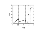
- FIG. 7 is a graph illustrating characteristics of the variable resistance element according to the first example of the invention. That is, this figure shows voltage-current characteristics when a pulse voltage is applied to the resistance change element 310a while gradually increasing.
- the horizontal axis is voltage
- the vertical axis is current.
- variable resistance element 310a As shown in FIG. 7, in the variable resistance element 310a, four voltages having different resistances were observed. That is, four voltages of about 0.6V, about 1.25V, about 1.45V, and about 1.65V.
- the initial state is the high resistance state, and when set, the low resistance state is set, and when reset, the high resistance state is set.
- the process of setting the low resistance state by setting may be called forming.
- the resistance change element 310a of this embodiment has four voltages at which the resistances are changed to different states, and a resistance change element capable of multi-value recording can be provided.
- the respective set voltages and reset voltages of the first resistance change layer 12A1 and the second resistance change layer 12A2 constituting the resistance change unit 12 are obtained as shown in Table 1.
- the electrical resistivity, the set, and the reset voltage of each layer were used as parameters, and the calculation was performed by fitting.
- the set voltage and the reset voltage of each resistance change layer have any resistance change.
- the layer is assigned as one of the resistance change layers.
- the reset voltage is 0.59V and the set voltage is 1.45V.
- the reset voltage is 1.25V and the set voltage is 1.65V.
- the reset voltage and the set voltage are different between the first resistance change layer 12A1 and the second resistance change layer 12A2 of the resistance change unit 12.
- the resistance change element 310a of the present embodiment can be used as a multi-value memory having four different resistance states.
- the characteristics shown in FIG. 7 and Table 1 are examples of characteristics in the case of unipolar operation.
- the voltage value having a different resistance value is different from that in the unipolar operation, but the bipolar operation is also possible.
- the first variable resistance layer 12A1 and the second variable resistance layer 12A2 are formed independently from each other. Further, since it is not always necessary to continuously form the lower electrode 11 and the first variable resistance layer 12A1 in a vacuum, a natural oxide film, that is, a TiOx is formed on TiN to be the lower electrode 11. (1 ⁇ x ⁇ 2) may be present.
- the composition of the interface between the first resistance change layer 12A1 or the second resistance change layer 12A2 and another film is slightly deviated from the above composition.
- the film in which about 10% of metal Mn is dispersed in Mn 3 O 4 used as the first resistance change layer 12A1 may be replaced with a film in which about 20% of MnO 2 is dispersed in Mn 3 O 4. it can. Further, a film in which about 5% of metal Mn is dispersed in Mn 3 O 4 can be substituted. Further, a film in which about 10% of MnO 2 is dispersed in Mn 3 O 4 can be substituted.
- variable resistance element (310b) of the second example according to this embodiment Zn 1.1 Mn 1.9 O 4 having a thickness of 20 nm is used for the first variable resistance layer 12A1, and the second variable resistance layer is used.
- 12A2 uses NiO having a thickness of 50 nm
- the lower electrode 11 uses TiN
- the upper electrode 13A uses Pt. It should be noted that NiO is accurately described as NiO 1- ⁇ (0 ⁇ ⁇ ⁇ 1), and the ratio of Ni and oxygen O may be slightly deviated from 1: 1.
- Table 2 shows the voltage-current characteristics of the resistance change film 310b of the second example having four different resistance states as illustrated in FIG. Thereby, the resistance change element 310b of the present embodiment can also be used as a multi-value memory having four different resistance states.
- the reset voltage was 0.6V and the set voltage was 1.7V.
- the reset voltage was 1.6V and the set voltage was 2.05V.
- the reset voltage and the set voltage are different in each of the first resistance change layer 12A1 and the second resistance change layer 12A2, and as a result, the four resistance states are changed.
- the thicknesses of the first and second resistance change layers 12A1 and 12A2 are a combination of 20 nm and 50 nm is shown, but these are suitable in the range of 5 nm or more and 50 nm or less, Thereby, the characteristic of the information recording / reproducing apparatus using the variable resistance element according to the present embodiment can be improved.
- the first resistance change layer 12A1 has a thickness of 30 nm and a 1: 1 mixture of microcrystalline graphite and amorphous carbon is used. .
- a 2: 1 mixture of microcrystalline graphite and amorphous carbon having a thickness of 30 nm is used for the second resistance change layer 12A2.
- TiN is used for both the lower electrode 11 and the upper electrode 13A.
- the mixture of microcrystalline graphite and amorphous carbon hardly reacts and remains in that state, except when heated to a temperature that cannot be experienced in a normal use environment, such as 1000 ° C. or higher.
- the mixture of microcrystalline graphite and amorphous carbon hardly reacts and remains in that state, except when heated to a temperature that cannot be experienced in a normal use environment, such as 1000 ° C. or higher.
- the resistance change element 310c of this example also exhibited voltage-current characteristics having four different resistance states, as illustrated in FIG. Thereby, the resistance change element 310c of the present embodiment can also be used as a multi-value memory having four different resistance states.
- the reset voltage was 0.4V and the set voltage was 1.2V in the first variable resistance layer 12A1.
- the reset voltage was 1.4V and the set voltage was 1.9V.
- the reset voltage and the set voltage are different in each of the first resistance change layer 12A1 and the second resistance change layer 12A2, and as a result, the four resistance states are changed.
- the thicknesses of the first and second resistance change layers 12A1 and 12A2 are a combination of 30 nm and 30 nm is shown, but these are suitable in the range of 5 nm or more and 50 nm or less, Thereby, the characteristic of the information recording / reproducing apparatus using the variable resistance element according to the present embodiment can be improved.
- the mixing ratio can be measured by various methods. For example, X-ray photoelectron spectroscopy (ESR) is performed by electron spin resonance (ESR) by cross-sectional TEM exploration by comparing the ratio of the peak of D-band and G-band or the ratio of area intensity by Raman spectroscopy. XPS) or electron beam energy loss spectroscopy (EELS). Further, by measuring the temperature change of the electrical resistivity, the mixing ratio of the microcrystalline graphite and the amorphous carbon can be estimated from the absolute value of the electrical resistivity and the temperature coefficient.
- ESR X-ray photoelectron spectroscopy
- ESR electron spin resonance
- EELS electron beam energy loss spectroscopy
- the electrical resistivity of the mixture of microcrystalline graphite and amorphous carbon was varied between 10 ⁇ 4 ⁇ cm and 10 2 ⁇ cm.
- the electrical resistivity of the mixture of microcrystalline graphite and amorphous carbon depends not only on the mixing ratio of microcrystalline graphite and amorphous carbon, but also on the crystal grain size of microcrystalline graphite and its graphitization degree.
- the crystal grain size of microcrystalline graphite has a different contribution to electrical resistivity even if the so-called in-plane direction and c-axis direction are different. In general, the electrical resistivity in the in-plane direction of graphite is lower than that in the c-axis direction.
- the crystal grain size of microcrystalline graphite is preferably 5 nm or less, more preferably 2 nm or less.
- a hydrocarbon method for example, a CVD method using a gas such as CH 4 or C 3 H 6 as a reaction gas, or a sputtering target of graphite (graphite) is used.
- the sputtering method used is preferable.
- the graphite component increases as the temperature is raised to 400 ° C, 500 ° C, and 600 ° C.
- the graphite component is unlikely to increase.
- hydrogen as a reactive gas component may remain in the film, but it is not uncommon for the amount to reach about 15 atomic percent (atomic percentage). Even in this case, it does not depart from the spirit of the present invention.
- graphite layer also called two-dimensional graphite or graphene
- GIC graphite intercalation compounds
- B nitrogen and boron
- carbon can take various forms such as diamond, dynemond-like carbon (DLC), fullerene, and carbon nano tube (CNT). Even if these are contained in trace amounts, they do not depart from the scope of the present invention.
- the first variable resistance layer 12A1 has a thickness of 0 nm and a 1: 1 mixture of microcrystalline graphite and amorphous carbon is used. It is done.
- a 1: 1 mixture of microcrystalline graphite and amorphous carbon having a thickness of 30 nm to which 2 atomic percent of nitrogen is added is used.
- TiN is used for both the lower electrode 11 and the upper electrode 13A.
- the resistance change film 310d of this example also exhibited voltage-current characteristics having four different resistance states, as illustrated in FIG. Thereby, the variable resistance element 310d of the present embodiment can also be used as a multi-value memory having four different resistance states.
- the reset voltage was 0.4V and the set voltage was 1.1V in the first resistance change layer 12A1.
- the reset voltage was 1.4V and the set voltage was 1.8V.
- the reset voltage and the set voltage are different in each of the first resistance change layer 12A1 and the second resistance change layer 12A2, and as a result, the four resistance states are changed.
- the thicknesses of the first and second resistance change layers 12A1 and 12A2 are a combination of 40 nm and 30 nm is shown, but these are suitable in the range of 5 nm or more and 50 nm or less, Thereby, the characteristic of the information recording / reproducing apparatus using the variable resistance element according to the present embodiment can be improved.
- the first resistance change layer 12A1 has a thickness of 40 nm and a 1: 1 mixture of microcrystalline graphite and amorphous carbon is used. .
- a 1: 1 mixture of microcrystalline graphite and amorphous carbon having a thickness of 30 nm and nitrogen added at 2 atomic percent is used.
- TiN is used for both the lower electrode 11 and the upper electrode 13A.
- the resistance change film 310e of this example also exhibited voltage-current characteristics having four different resistance states, as illustrated in FIG. Thereby, the resistance change element 310e of the present embodiment can also be used as a multi-value memory having four different resistance states.
- the reset voltage was 0.4V and the set voltage was 1.1V in the first variable resistance layer 12A1.
- the reset voltage was 1.3V and the set voltage was 2.0V.
- the reset voltage and the set voltage are different in each of the first resistance change layer 12A1 and the second resistance change layer 12A2, and as a result, the four resistance states are changed.
- the thicknesses of the first and second resistance change layers 12A1 and 12A2 are a combination of 40 nm and 30 nm is shown, but these are suitable in the range of 5 nm or more and 50 nm or less, Thereby, the characteristic of the information recording / reproducing apparatus using the variable resistance element according to the present embodiment can be improved.
- the first resistance change layer 12A1 has a thickness of 40 nm and a 1: 1 mixture of microcrystalline graphite and amorphous carbon is used. .
- a 2: 1 mixture of microcrystalline graphite and amorphous carbon having a thickness of 40 nm and boron (B) added at 3 atomic percent is used.
- TiN is used for both the lower electrode 11 and the upper electrode 13A.
- the resistance change film 310f of this example also exhibited voltage-current characteristics having four different resistance states, as illustrated in FIG. Thereby, the variable resistance element 310f of the present embodiment can also be used as a multi-value memory having four different resistance states.
- the reset voltage was 0.4V and the set voltage was 1.1V in the first variable resistance layer 12A1.
- the reset voltage was 1.4V and the set voltage was 1.8V.
- variable resistance element 310f of this example the reset voltage and the set voltage are different in each of the first variable resistance layer 12A1 and the second variable resistance layer 12A2, and as a result, the four resistance states are changed.
- a threshold voltage which can be used as a multi-value memory having four different states.
- the thicknesses of the first and second resistance change layers 12A1 and 12A2 are a combination of 40 nm and 40 nm is shown, but these are suitable in the range of 5 nm or more and 50 nm or less, Thereby, the characteristic of the information recording / reproducing apparatus using the variable resistance element according to the present embodiment can be improved.
- variable resistance element of the first comparative example the variable resistance portion 12 is made of one type of material. That is, the resistance change layer 12 is made of only a material of 20 nm thick Mn 1.9 O 3 . Except this, it is the same as the resistance change element 310a of the first embodiment.
- the reset voltage during the unipolar operation was about + 0.5V, and the set voltage was about + 1.5V.
- the reset voltage during bipolar operation was about + 0.5V and the set voltage was about -0.5V.
- the stability of the characteristics in the repeated energization cycle was poor, and the above operation was performed for each element several hundred times. I can't do it.
- multi-value information cannot be recorded and reproduced in one resistance change element.
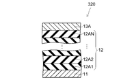
- FIG. 8 is a schematic cross-sectional view illustrating the configuration of a resistance change element according to the second embodiment of the invention.
- the first resistance change layer 12A1, the second resistance change layer 12A2,... Nth resistance are formed on the lower electrode 11.
- the change layer 12AN is sequentially stacked, and the upper electrode 13A is stacked on the uppermost Nth resistance change layer 12AN.
- N is an integer of 2 or more.
- the resistance change unit 12 includes a plurality of resistance change layers having different compositions and different electrical characteristics. That is, the first resistance change layer 12A1, the second resistance change layer 12A2,... The Nth resistance change layer 12AN have different compositions.
- the resistance change element 320 since the resistance change element 320 according to this embodiment includes N resistance change layers having different characteristics, the resistance change element 320 has 2 N different states.
- the state of the lowermost first resistance change layer 12A1 is LSB and the state of the uppermost Nth resistance change layer 12AN is MSB, which functions as an N-bit memory cell.
- variable resistance portion 12 can have a plurality of arbitrary variable resistance layers having different compositions and different electrical characteristics.
- FIG. 9 is a schematic cross-sectional view illustrating the configuration of a variable resistance element according to the third embodiment of the invention.
- the resistance change element 330 according to the third embodiment of the present invention, the first resistance change layer 12A1 and the second resistance change layer 12A2 are provided, and an interlayer separation layer is provided therebetween.
- (Separation layer) 12C1 is provided.
- the description is omitted.
- interlayer separation layer 12C a material different from the resident tail used for the first resistance change layer 12A1 and the second resistance change layer 12A2 can be used.
- various metal films can be used for the interlayer separation layer 12C1.
- the first resistance change layer 12A1 and the first resistance change layer are provided. Diffusion of elements between 12A2 can be suppressed. Thereby, there is an effect that heat resistance, environment resistance, and rewriting durability are increased.
- the crystallinity of the resistance change portion 12 is improved, and variations between elements and lots can be greatly reduced.
- the resistance change element 330 according to the present embodiment, multi-value recording is possible, the performance is stable, and the resistance change element having a high number of rewrites can be provided.
- Example 7 The variable resistance element 330a of the seventh example according to this embodiment was produced.
- the lower electrode 11, the first resistance change layer 12A1, the second resistance change layer 12A1, and the upper electrode 13A have the same configuration as the resistance change element 310b of the second embodiment.
- an interlayer separation layer 12C1 between the first resistance change layer 12A and the second resistance change layer 12A2 a film in which 6 atomic percent of Al was added to ZnO was formed to a thickness of 2 nm.
- the characteristics of the resistance change element 330a of the present example produced in this way are substantially the same as the first to fourth threshold voltages of the resistance change element 310b of the second example.
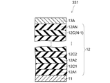
- FIG. 10 is a schematic cross-sectional view illustrating the configuration of another variable resistance element according to the third embodiment of the invention.
- the resistance change unit 12 includes three or more resistance change layers. In between, the above-mentioned interlayer separation layer is provided.
- variable resistance part 12 of the variable resistance element 311 includes a first variable resistance layer 12A1, a second variable resistance layer 12A2,... An Nth variable resistance layer 12AN, and a first interlayer separation layer 12C1 therebetween.
- Second interlayer isolation layer 12C2... (N-1) interlayer isolation layer 12C (N-1) are provided.
- the crystallinity of each layer of the resistance change portion 12 is improved, and variations between elements and lots can be greatly reduced.
- resistance change element 331 According to another resistance change element 331 according to the present embodiment, multi-value recording with a higher number of bits is possible, a resistance change element with a stable performance and a high number of rewrites can be provided.
- FIG. 11 is a schematic cross-sectional view illustrating the configuration of a variable resistance element according to the fourth embodiment of the invention.
- the resistance change element 340 according to the fourth exemplary embodiment of the present invention includes an electrode side separation between the lower electrode 11 and the first resistance change layer 12 ⁇ / b> A ⁇ b> 1 in the resistance change element 330.
- Layer 12C0 is provided.
- the electrode-side separation layer (separation layer) 12C0 between the lower electrode 11 and the first resistance change layer 12A1
- the diffusion of elements between the lower electrode 11 and the first resistance change layer 12A1 is reduced. It is possible to prevent heat resistance, environmental resistance, and rewriting durability.
- first interlayer separation layer 12C1 to Nth interlayer separation layer 12CN and electrode side separation layer 12C0 are collectively referred to as a separation layer 12C.
- Example 8 A variable resistance element 340a according to an eighth example of the fourth embodiment of the present invention was produced. At this time, a material in which Sb 2 O 3 was added at 5 atomic percent to SnO 2 was used for the electrode-side separation layer 12C0. Other than that, it is the same as the variable resistance element 330a of the seventh embodiment.
- Zn 1.1 Mn 1.9 O 4 with a thickness of 20 nm is used for the first resistance change layer 12A2
- NiO with a thickness of 50 nm is used for the second resistance change layer 12A2
- TiN is used for the lower electrode 11.
- Pt is used for the upper electrode 13A.
- the reset voltage and set voltage of the variable resistance element 340a having the above configuration are the same as those in Table 2 and are different from each other. Therefore, as in the first to seventh embodiments, so-called multi-value information can be recorded and reproduced.
- Example 9 As a ninth example according to the fourth embodiment of the present invention, variable resistance elements having various configurations were produced. That is, TiN is used for the lower electrode 11, a 20 nm-thick film in which Mn of metal is dispersed in Mn 3 O 4 is used for the first resistance change layer 12A1, and Mn is used for the second resistance change layer 12A2. A 20 nm thick film in which MnO 2 was dispersed in 3 O 4 was used, and Pt was used for the upper electrode 13A. At this time, Mn 3 O 4 ratio of metal of Mn to be dispersed in, and to prepare a sample with different ratio of MnO 2 dispersed in the Mn 3 O 4.
- a mixed film of TiOs (1 ⁇ s ⁇ 2) and SnO 2 having a thickness of 1 nm was used for the interlayer separation layer 12C1 and the separation layer 12C0.
- a mixed film of ZnO and Al 2 O 3 also referred to as ZnO doped with Al
- a mixed film of ZnO and Ga 2 O 3 this is doped with ZnO with Ga
- film of a mixture of Sb 2 O 3 to SnO 2 the in 2 O 3
- a film obtained by mixing, IrO 2 and Ir mixed film, and RuO 2 and Ru mixed film were used.
- Table 7 shows the measurement results of the reset voltage and set voltage of these first and second resistance change layers.
- the ratio of the metal Mn dispersed in Mn 3 O 4, and controls the Mn 3 O 4 ratio and dispersion state of MnO 2 dispersed in such also, the interlayer separating layer 12C1 and the separation layer 12C0 used materials Is changed, the reset voltage and the set voltage of each variable resistance layer of the variable resistance element are controlled.
- the thickness of each variable resistance layer is also controlled to an appropriate value so that the reset voltage and the set voltage fall within a predetermined range as exemplified in Table 7.
- Samples 1 to 14 shown in Table 7 were capable of multi-value recording and reproduction as well as the resistance change element 310a of the first example, for example.
- variable resistance elements All of the variable resistance elements were observed to have a stable rewrite operation of several thousand times or more, and could be rewritten more times.
- the difference between the reset voltage of one of the first variable resistance layer 12A1 and the second variable resistance layer 12A2 and the set voltage of the other is the repetitive operation.
- 0.1 V or more is desirable, although it depends on variations in resistance, variations between resistance change elements, and also in the pulse operation, such as the magnitude of noise components such as ringing. .
- the effect of the film thickness of the interlayer separation layer 12C1 and the separation layer 12C0 is 0.5 nm or more. That is, when the thickness is 50 nm or more, the state of the resistance change layers (first resistance change layer 12A1 and second resistance change layer 12A2) in contact with the interlayer isolation layer 12C1 and the isolation layer 12C0 is changed. In view of manufacturing requirements, it is desirable that the thickness of the interlayer separation layer 12C1 and the separation layer 12C0 be too large. The most preferable range is about 1 to 5 nm. There was no.
- the thickness of the interlayer separation layer 12C1 and the separation layer 12C0 is preferably 0.5 nm or more and 50 nm or less.
- the thickness of the first variable resistance layer 12A1 and the second variable resistance layer 12A2 is a combination of 20 nm and 50 nm is exemplified, but these are suitable information recording / reproducing in the range of 5 nm or more and 50 nm or less. It can be a device.
- the reset voltage of the first resistance change layer 12A1 and the second resistance change layer 12A2 of the resistance change unit 12 is the same at 0.5 V, and the first resistance change layer 12A1 of the resistance change unit 12 and A sample having the same configuration with the second variable resistance layer 12A2 having a set voltage of 1.8 V was evaluated.
- the reset voltage of the resistance change unit 12 is about + 0.5V, and the reset voltage is about + 1.8V. Also, multi-value information could not be recorded and reproduced.
- any of the first to ninth embodiments as the information recording / reproducing apparatus, it was possible to record and reproduce multi-value information by controlling the characteristics of the recording film.
- the power consumption can be reduced as compared with the prior art, and the present embodiment is remarkably superior in view of cycle characteristics.
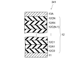
- FIG. 12 is a schematic cross-sectional view illustrating the configuration of another variable resistance element according to the fourth embodiment of the invention.
- the resistance change unit 12 includes N resistance change layers (first to Nth resistance changes 12A1 to 12AN).
- the interlayer separation layers 12C1 to 12C (N-1) are provided between the resistance change layers, the isolation layer 12C0 is provided between the resistance change portion 12 and the lower electrode 11, and the resistance change portion 12 A separation layer 12CN is provided between the upper electrode 13A.
- an interlayer separation layer can be provided between any N variable resistance layers.
- an interlayer separation layer may not be provided between all of the N resistance change layers, and may be provided at an arbitrary position.
- a separation layer can be provided between any of the lower electrode 11 and the upper electrode 13.
- the first to Nth interlayer separation layers 12C1 to 12C (N-1) are collectively referred to as an interlayer separation layer 12C.
- the separation layer 12C0 may also be used as at least one of the lower electrode 11 and the upper electrode 13A.
- FIG. 13 is a schematic cross-sectional view illustrating the configuration of a resistance change element according to the fifth embodiment of the invention.
- the current limiting layer 12 ⁇ / b> D is provided between the lower electrode 11 and the first resistance change layer 12 ⁇ / b> A ⁇ b> 1.
- variable resistance element for example, when only the first variable resistance layer 12A1 changes from the erased state to the set state, it is applied to both the first variable resistance layer 12A1 and the second variable resistance layer 12A2.
- the voltage is applied only to the second resistance change layer 12A2, and a rush current flows.
- the second resistance change layer 12A2 may be reset at the same time. Therefore, in the variable resistance element 350 according to the present embodiment, a current limiting layer 12D is provided between the lower electrode 11 and the variable resistance portion 12 in order to limit such a rush current.
- a transistor or a diode that is an active device can be used, but a so-called resistance layer that increases the electric resistance of the element electric conductor including the resistance change element can be used.
- the current limiting layer 12D can be provided between at least one of the lower electrode 11 and the resistance change portion 12 and between the resistance change portion 12 and the upper electrode 13A.
- the current can be limited by a driver circuit using a transistor, a diode, a resistor, and a capacitor in an information recording / reproducing apparatus to which a variable resistance element is applied.
- FIG. 14 is a schematic cross-sectional view illustrating the configuration of another variable resistance element according to the fifth embodiment of the invention.
- the resistance change unit 12 includes N resistance change layers (first to Nth resistance changes 12A1 to 12AN). Interlayer separation layers 12C1 to 12C (N-1) are provided between the respective resistance change layers, and a current limiting layer 12D is provided between the lower electrode 12 and the first resistance change layer 12A1.
- the current limiting layer 12D may be provided between the resistance change layer 12D and the upper electrode 13A, and the current limiting layer 12D may be provided at any place between the lower electrode 11 and the upper electrode 13A. Any number of current limiting layers 12D can be provided.
- FIG. 15 is a schematic cross-sectional view illustrating the configuration of a resistance change element according to the sixth embodiment of the invention.
- the resistance change element 360 according to the sixth exemplary embodiment of the present invention includes an orientation control layer 11 ⁇ / b> A that controls the orientation of the resistance change layer between the lower electrode 11 and the first recording element 12 ⁇ / b> A ⁇ b> 1. Is provided.
- orientation control layer 11A for example, compounds of various metals and nitrogen can be used, thereby improving the orientation of the resistance change layer and obtaining a resistance change layer with good characteristics with good reproducibility.
- variable resistance element 360 In the information recording / reproducing apparatus to which the variable resistance element 360 according to this embodiment is applied, multi-value recording is performed. At this time, the variable resistance element 360 is required to have high quality, and for this purpose, it is very important that the characteristics of the plurality of variable resistance layers are stabilized. At this time, in the resistance change element 360 according to the present embodiment, the orientation control layer 11D is provided to stabilize the quality of the resistance change layer. Thereby, the resistance change element which enables multi-value recording with high quality can be resisted.
- FIG. 16 is a schematic cross-sectional view illustrating the configuration of a resistance change element according to the seventh embodiment of the invention.
- the first resistance change layer 12A1 and the second resistance change layer 12A2 are adjacent to each other, respectively.
- a 1 ion storage layer 12B1 and a second ion storage layer 12B2 are provided.
- the first ion storage layer 12B1 and the second ion storage layer 12A2 have a function of storing ions discharged from the first resistance change layer 12A1 and the second resistance change layer 12A2, and an effect of facilitating the movement of ions.
- the material to be used it is possible to always have high electron conductivity regardless of the entry and exit of ions, and also to have the effect of ensuring the stability of the crystal structure. As a result, it is possible to improve the disturbance resistance due to reverse voltage application.
- the first ion storage layer 12B1 is provided adjacent to the first resistance change layer 12A1. As shown in FIG.
- the second ion storage layer 12B2 is provided adjacent to the second resistance change layer 12A2.
- an ion storage layer may be provided in at least one of the first resistance change layer 12A1 and the second resistance change layer 12A2.
- the resistance change unit 12 includes N resistance change layers, that is, first to Nth resistance change layers 12A1 to 12AN.
- the first to Nth ion storage layers 12B1 to 12BN are provided in at least one of the first to Nth resistance change layers 12A1 to 12AN, respectively.
- variable resistance layer 12A The first to Nth variable resistance layers 12A1 to 12AN are collectively referred to as the variable resistance layer 12A.
- the first to Nth ion storage layers 12B1 to 12BN are collectively referred to as the ion storage layer 12B.
- a resistance change element having a stable resistance change operation can be provided.
- first ion storage layer 12A1 and the second ion storage layer 12A2 Materials that can be used for the first ion storage layer 12A1 and the second ion storage layer 12A2 will be described later.
- FIG. 17 is a schematic view illustrating the configuration and operation of a part of the variable resistance element according to the embodiment of the invention.
- the operation in one resistance change layer is illustrated, so that one resistance change layer (resistance change portion 12) is provided between the lower electrode 11 and the upper electrode 13A.
- one resistance change layer resistance change portion 12
- the recording unit (resistance change unit) 12 includes a first type layer 81, and the first type layer 81 includes diffusion ions 52 (A ions) and transition element ions 51 ( M ion) and a first type compound 71 having anion 61 (X ion).
- the compound used for the resistance change layer 12A is composed of, for example, a composite compound having at least two types of cation elements, and at least one of the cation elements has a d orbital in which electrons are incompletely filled.
- the compound used for the recording layer 12A is composed of a composite compound having at least two kinds of cation elements, and at least one of the cation elements is d orbital in which electrons are incompletely filled. It can be set as the electroconductive oxide containing the transition element which has.
- the initial state is set to the high resistance state HR
- the state of the recording unit 12 is changed by the potential gradient formed in the recording unit 12, and the recording unit 12 is made conductive to be in the low resistance state LR.
- An example of a mechanism for recording information will be described.
- the set operation SO for example, a state in which the potential of the upper electrode 13A is relatively lower than the potential of the lower electrode 11 is created. That is, for example, the lower electrode 11 is set to a fixed potential (for example, ground potential), and a negative potential is applied to the upper electrode 13A.
- a fixed potential for example, ground potential
- the diffused ions 52 that have moved to the upper electrode 13A side receive electrons from the upper electrode 13A and are deposited as metal (A metal 52m) to form the metal layer 14.
- the anions 61 become excessive, and as a result, the valence of the transition element ions 51 in the recording unit 12 is increased. That is, since the recording unit 12 has electron conductivity due to carrier injection, the recording unit 12 is set and information recording is completed.
- Information reproduction is performed by passing a current pulse through the recording unit 12 and detecting the resistance value of the recording unit 12.
- the current pulse is set to such a minute value that the material constituting the recording unit 12 does not change state.
- the above process is a kind of electrolysis, and an oxidizing agent is produced by electrochemical oxidation on the lower electrode (anode) 11 side, and a reducing agent is produced by electrochemical reduction on the upper electrode (cathode) 13A side. It can be considered that it has occurred.
- the recording unit 12 in order to return the information recording state (low resistance state LR) to the initial state (high resistance state HR), for example, the recording unit 12 is Joule-heated by a large current pulse, and the redox reaction of the recording unit 12 is performed. It should be promoted. That is, the recording unit 12 returns to the high resistance state HR due to the residual heat after the interruption of the large current pulse (reset operation RO).
- the retention time is sufficiently long so that the reset operation RO does not occur at room temperature. And the power consumption of the reset operation RO is reduced.
- the coordination number of the diffusion ions 52 is reduced (ideally 2 or less), the valence is 2 or more, or the anion 61 is increased (ideally 3). By doing so, the retention time can be sufficiently reduced.
- the valence of the diffusion ions 52 is set to 2 or less, and at the same time, the above consumption is achieved by using a material having many movement paths of the diffusion ions 52 moving in the recording portion (crystal) 12. Electric power can be made sufficiently small.
- an element and crystal structure as described below and an ion storage layer may be employed.
- At least one of the materials represented by the following (1) to (3) can be used for each layer (each resistance change layer) of the recording portion (resistance change portion) 12.
- a x M y X 4 (0.1 ⁇ x ⁇ 2.2,1.8 ⁇ y ⁇ 2)
- A is Na, K, Rb, Be, Mg, Ca, Sr, Ba, Al, Ga, Mn, Fe, Co, Ni, Cu, Zn, Ge, Ag, Au, Cd, Sn, Sb
- M is Al, Ga, Ti, Ge, Sn, V, Cr, Mn, Fe, Co
- the X is an element including at least one selected from the group consisting of O and N , A and M are different elements.
- a x M y X 3 (0.5 ⁇ x ⁇ 1.1,0.9 ⁇ y ⁇ 1)
- A is Na, K, Rb, Be, Mg, Ca, Sr, Ba, Al, Ga, Mn, Fe, Co, Ni, Cu, Zn, Ge, Ag, Au, Cd, Sn, Sb
- M is Al, Ga, Ti, Ge, Sn, V, Cr, Mn, Fe, Co
- X is an element including at least one selected from the group consisting of O and N , A and M are different elements.
- a x M y X 4 (0.5 ⁇ x ⁇ 1.1,0.9 ⁇ y ⁇ 1)
- A is at least any selected from the group consisting of Mg, Ca, Sr, Al, Ga, Sb, Ti, V, Cr, Mn, Fe, Co, Rh, In, Sb, Tl, Pb, and Bi.
- M is an element containing at least one selected from the group consisting of Al, Ga, Ti, Ge, Sn, V, Nb, Ta, Cr, Mn, Mo, W, Ir, and Os.
- X is an element containing at least one selected from the group consisting of O and N, and A and M are different elements.
- each layer (each resistance change layer) of the recording part (resistance change part) 12 includes a corundum structure, a rutile structure, a spinel structure, a ramsdellite structure, an anatase structure, a hollandite structure, a brookite structure, a pyrolose structure, a NaC structure, and a probeskite. It may have a crystal structure having any structure selected from the group consisting of a structure, an ilmenite structure, and a wolframite structure.
- each of the plurality of resistance change layers 12A (first resistance change layer 12A1 to Nth resistance change layer 12AN) of the resistance change element according to the first to seventh embodiments the materials and configurations exemplified above are used. Of these, at least one of different materials, different component ratios, and different configurations is used. Accordingly, at least one of the set voltage and the reset voltage can be made different in each of the plurality of resistance change layers 12A (first resistance change layer 12A1 to Nth resistance change layer 12AN).
- FIG. 18 is a schematic cross-sectional view illustrating the configuration and operation of a part of the variable resistance element according to the embodiment of the invention. That is, this figure schematically illustrates the action of the ion storage layer 12B in the resistance change element, and the resistance change layer 12A is a single layer and the ion storage layer 12B is a single layer.
- an ion storage layer 12B is provided adjacent to the resistance change layer 12A.
- the ion storage layer 12B includes a second type layer 82.
- the second type layer 82 includes transition metal ions 53 and anions 61, and can further store A ions 52 that the resistance change layer 12A moves. It consists of a second type of compound 72 having a void site ⁇ . Thereby, in the set operation (SO), the A ions 52 that have moved from the resistance change layer 12A are stored in the void sites ⁇ of the ion storage layer 12B.
- FIG. 19 is a schematic cross-sectional view illustrating the configuration and operation of a part of another variable resistance element according to an embodiment of the invention.
- the first resistance change layer 12A1 to the Nth resistance change layer 12A2 is an ion. It has a storage layer (first ion storage layer 12B1 to Nth ion storage layer 12BN).
- first ion storage layer 12B1 to Nth ion storage layer 12BN is an ion.
- each A ion 52 of the plurality of resistance change layers 12A can be stored in the void site ⁇ of the ion storage layer 12B adjacent thereto, and two states of a high resistance state and a low resistance state can be obtained. It can be expressed stably.
- the ion storage layer 12B is preferably made of, for example, a conductive oxide.
- the resistivity of the conductive oxide layer is less than the resistivity of the resistance change layer 12A, and preferably 10-1 ⁇ cm or less.
- the ion storage layer 12B is characterized by having a void site ⁇ . However, the gap site ⁇ may be partially filled with cations that have moved from the resistance change layer 12A.
- the ion storage layer 12B at least one of the materials represented by the following (4) to (6) can be used.
- A is at least one element selected from the group consisting of Ti, Zr, Hf and Sn
- M is a group consisting of V, Nb, Ta, Cr, Mo, W, As, Sb and Bi.
- X is at least one element selected from the group consisting of O, N and F, and is an element different from A and M, and 0.001 ⁇ x ⁇ 0.2 and 0 ⁇ u ⁇ 0.2.
- a 2-x M x X 3-u A is at least one element selected from the group consisting of V, Nb, Ta, Cr, Mo, W, Mn, Fe, Co, Ga and In, and M is Ti, Zr, Hf, At least one element selected from the group consisting of Sn, V, Nb, Ta, As, Sb, Bi, Cr, Mo and W, and X is at least selected from the group consisting of O, N and F
- One element, different from A and M 0.001 ⁇ x ⁇ 0.2 and 0 ⁇ u ⁇ 0.3.
- a 2-x M x X 5-u A is at least one element selected from the group consisting of V, Nb and Ta, M is at least one element selected from the group consisting of Cr, Mo and W, and X is , O, N and F are at least one element selected from the group consisting of A and M, and 0.001 ⁇ x ⁇ 0.2 and 0 ⁇ u ⁇ 0.5 .
- these materials have a function of storing ions ejected from the resistance change layer 12A, they have an effect of facilitating the movement of ions and limit the composition range to x> 0.001. Regardless of going in and out, it always has an electron conductivity of 10 S / cm or more, and has an effect of ensuring the stability of the crystal structure by limiting the composition range to x ⁇ 0.2. As a result, it is possible to improve the disturbance resistance by applying the reverse voltage.
- the following materials can be used for the lower electrode 11. That is, since an oxidant is generated on the lower electrode (anode) 11 side after the set operation SO, the lower electrode 11 is made of a material that is not easily oxidized (for example, electrically conductive nitride, electrically conductive oxide, etc.). It is preferable to configure.
- the electrode layer 11 is preferably made of a material that does not have ion conductivity.
- LaNiO 3 can be said to be the most preferable material from the viewpoint of comprehensive performance including good electrical conductivity and the like.
- At least one of the materials represented by the following (7) to (10) can be used.
- MN includes at least one element selected from the group consisting of Ti, Zr, Hf, V, Nb, and Ta, and N is nitrogen.
- MO x consists of Ti, V, Cr, Mn, Fe, Co, Ni, Cu, Zr, Nb, Mo, Ru, Rh, Pd, Ag, Hf, Ta, W, Re, Ir, Os, and Pt. It includes at least one element selected from the group, and the molar ratio x satisfies 1 ⁇ x ⁇ 4.
- AMO 3 contains at least one element selected from the group consisting of La, K, Ca, Sr, Ba and Ln (Lanthanide), and M is Ti, V, Cr, Mn, Fe, Co, Ni , Cu, Zr, Nb, Mo, Ru, Rh, Pd, Ag, Hf, Ta, W, Re, Ir, Os and Pt, and at least one element selected from the group consisting of Pt, O is oxygen is there.
- B contains at least 1 type of element selected from the group which consists of K, Ca, Sr, Ba, and Ln (Lanthanide), M is Ti, V, Cr, Mn, Fe, Co, Ni, Cu And at least one element selected from the group consisting of Zr, Nb, Mo, Ru, Rh, Pd, Ag, Hf, Ta, W, Re, Ir, Os, and Pt, and O is oxygen.
- the lower electrode 11 can be made of metal such as Au, Ru, Ir and W.
- the upper electrode 13A preferably has a function of preventing the recording unit 12 from reacting with the atmosphere.
- Examples of such a material include semiconductors such as amorphous carbon, diamond-like carbon, and SnO 2 .
- metals such as Au, Ru, Ir and W can also be used for the upper electrode 13A.
- the upper electrode 13A may function as a protective layer for protecting the recording unit 12, or a protective layer may be provided instead of the upper electrode 13A.
- the protective layer may be an insulator or a conductor.
- the lower electrode 11 and the upper electrode 13A can be interchanged with each other, and materials that can be used for the lower electrode 11 and the upper electrode 13A can be interchanged with each other.
- TiSiN, TaN, TaSiN, and WN can be used for the lower electrode 11 and the upper electrode 13A in addition to the materials described in the embodiments.
- SiN, TiC, TaC, and SiC are also suitable, and mixing these is also suitable.
- Metals such as Au, Ru, Ir, and W can also be used for the lower electrode 11 and the upper electrode 13A.
- the lower electrode 11 and the upper electrode 13A include Ti—N, Ti—Si—N, Ta—N, Ta—Si—N, Si—N, Ti—N, Ta—C, Si—C, and W—.
- At least one selected from the group consisting of N, nitride, carbide, oxide, and a mixture of at least two of nitride, carbide, and oxide can be used. . That is, at least one nitride selected from the group, carbide, oxide, a mixture of nitride and oxide, a mixture of nitride and carbide, a mixture of oxide and carbide, or Any of a mixture of nitride, carbide and oxide can be used.
- the separation layer 12C that is, the interlayer separation layer 12C (the first interlayer separation layer 12C1 to the Nth separation layer 12CN) and the separation layer 12C0 are Ti—N, Ti—Si—N, Ta—N, Ta—Si—. N, Si—N, Ti—C, Ta—C, Si—C, and at least one nitride selected from the group consisting of W—N, carbide, oxide, and nitride, carbide, and oxide And / or a mixture of at least two of them.
- the separation layer 12C was selected from the group consisting of ZnO, SnO 2 , In 2 O 3 , TiO s (1 ⁇ s ⁇ 2), In 2 O 3 , IrO 2 , RuO 2 , Ir, Ru, and Ta. At least one of them can be included.
- the separation layer 12C can use at least one selected from the group consisting of Ga 2 O 3 , Al 2 O 3 , Nb 2 O 5 , SnO 2 , Ta 2 O 5 and Sb 2 O 3 .
- the separation layer 12C can include at least one selected from the group consisting of W, Ta, Si, Ir, Ru, Au, Pt, Pd, Mo, Ni, Cr, and Co.
- an information recording / reproducing apparatus for a probe memory, a semiconductor memory, and a flash memory using at least one of the resistance change elements of the first to seventh embodiments will be described.
- the seventh embodiment of the present invention is a probe memory type information recording / reproducing apparatus.
- FIG. 20 is a schematic perspective view illustrating the configuration of the information recording / reproducing apparatus according to the eighth embodiment of the invention.
- FIG. 21 is a schematic plan view illustrating the configuration of part of the information recording / reproducing apparatus according to the eighth embodiment of the invention.
- FIG. 22 is a schematic view illustrating the operation of the information recording / reproducing apparatus according to the eighth embodiment of the invention.
- FIG. 23 is a schematic view illustrating the recording operation of the information recording / reproducing apparatus according to the eighth embodiment of the invention.
- FIG. 24 is a schematic view illustrating the reproducing operation of the information recording / reproducing apparatus according to the eighth embodiment of the invention.
- any of the first to seventh embodiments of the present invention is placed on the XY scanner 516.
- a recording medium 410 provided with the variable resistance element 310 is disposed.
- a probe array is arranged to face the recording medium 410.
- the recording medium 410 includes, for example, a substrate 520, an electrode layer 521 on the substrate 520, and a first resistance change layer 12A1 and a second resistance change layer 12A2 on the electrode layer 521.
- the electrode layer 521 the lower electrode 11 described in the first to sixth embodiments can be used. That is, the recording medium 410 is obtained by providing the resistance change element according to the first to seventh embodiments on the substrate 520.
- the variable resistance element 310 according to the first embodiment will be described.
- the protective layer 13B is made of, for example, a thin insulator.
- the probe array has a substrate 523 and a plurality of probes (heads) 524 arranged in an array on one surface side of the substrate 523.
- Each of the plurality of probes 524 is composed of a cantilever, for example, and is driven by multiplex drivers 525 and 526.
- Each of the plurality of probes 524 can be individually operated by using the microactuator in the substrate 523.
- an example in which all of the probes 524 are collectively operated to access the data area of the recording medium 410 will be described. To do.
- all the probes 524 are reciprocated in the X direction at a constant period, and the position information in the Y direction is read from the servo area of the recording medium 410.
- the position information in the Y direction is transferred to the driver 515.
- the driver 15 drives the XY scanner 516 based on this position information, moves the recording medium 410 in the Y direction, and positions the recording medium 419 and the probe 524.
- Data reading and writing are continuously performed because the probe 524 is reciprocating in the X direction. Data reading and writing are performed on the data area 531 line by line by sequentially changing the position of the recording medium 410 in the Y direction.
- the recording medium 410 may be reciprocated in the X direction at a constant cycle to read position information from the recording medium 410, and the probe 524 may be moved in the Y direction.
- the resistance change element 310 includes a plurality of data areas 531 and servo areas 532 arranged at both ends of the plurality of data areas 531 in the X direction.
- the plurality of data areas 531 occupy the main part of the recording medium 410.
- Servo burst signals are recorded in the servo area 531.
- the servo burst signal indicates position information in the Y direction within the data area 531.
- variable resistance element 310 in addition to these pieces of information, an address area in which address data is recorded and a preamble area for synchronization are arranged.
- the data and servo burst signal are recorded in the resistance change element 310 as recording bits (electrical resistance fluctuation).
- Information of “3”, “2”, “1”, “0” of the recording bit is read by detecting the electric resistance of the variable resistance element 310 and quantizing the quaternary information.
- one probe (head) is provided corresponding to one data area 531, and one probe is provided for one servo area 532.
- the data area 531 is composed of a plurality of tracks.
- the track of the data area 531 is specified by the address signal read from the address area.
- the servo burst signal read from the servo area 532 is for moving the probe 524 to the center of the track and eliminating the recording bit reading error.
- the X direction correspond to the down-track direction and the Y direction correspond to the track direction, it becomes possible to use the HDD head position control technology.
- Each probe 524 is connected to the drive unit 600 via, for example, multiplex drivers 525 and 526.
- the drive unit 600 supplies each probe 524 with at least one of voltage and current for information recording. Then, the recording unit 12 of the resistance change element 310 transitions between three or more resistance states according to the voltage and current applied via the probe 524.
- the drive unit 600 detects three or more resistance states recorded in the recording unit 12 and reads the recorded information.
- the information recording / reproducing apparatus 210 includes at least one of the resistance change elements according to the first to seventh embodiments, application of a voltage to the recording unit of the resistance change element, A drive unit 600 is provided that records information by causing the recording unit to transition between three or more resistance states by at least one of supplying a current to the recording unit.
- the information recording / reproducing apparatus 210 further includes a probe 524 attached to the resistance change element, and the drive unit 600 applies a voltage to the recording unit of the resistance change element via the probe 524, and At least one of current supply to the recording unit is performed.
- the information recording / reproducing apparatus 210 uses at least one of the resistance change elements according to the first to seventh embodiments, it is possible to provide an information recording / reproducing apparatus that enables multi-value recording.
- FIG. 22 conceptually illustrates the recording operation (set operation SO).
- the recording operation is performed by applying a voltage to the surface of the recording bit 527 of the variable resistance element 310 to generate a potential gradient inside the recording bit 527.
- a current or voltage pulse is applied to the resistance change section 12 (first resistance change layer 12A1 and second resistance change layer 12A2) of the resistance change element 310 to be the recording bit 527 through the probe 524.
- FIG. 23 conceptually illustrates the recording operation.
- a state in which the potential of the probe 524 is relatively lower than the potential of the electrode layer 521 is created.
- the electrode layer 521 is set to a fixed potential (eg, ground potential)
- a negative potential may be applied to the probe 524.
- the current pulse is generated by emitting electrons from the probe 524 toward the electrode layer 521 using, for example, an electron generation source or a hot electron source.
- the voltage pulse may be applied by bringing the probe 524 into contact with the surface of the recording bit 527.
- the A ions 52 moves to the probe (cathode) 524 side and crystal (resistance change)
- the A ions 52 in the layer 12A) decrease relative to the X ions 61.
- the A ions 52 that have moved to the probe 24 side receive electrons from the probe 524 and are deposited as metal.
- the X ion 61 becomes excessive, and as a result, the valence of the A ion 52 or the M ion 51 in the recording bit 527 is increased. That is, since the recording bit 527 has electron conductivity due to carrier injection due to phase change, resistance in the film thickness direction is reduced, and recording (set operation) is completed.
- the current pulse for recording can be generated by creating a state in which the potential of the probe 524 is relatively higher than the potential of the electrode layer 521.
- FIG. 24 conceptually illustrates the reproduction operation. Reproduction is performed by passing a current pulse through the recording bit 527 of the variable resistance element 310 and detecting the resistance value of the recording bit 527. However, the current pulse is set to a minute value such that the resistance change element 310 used for the recording bit 527 does not change in resistance.
- a read current (current pulse) generated by the sense amplifier S / A is passed from the probe 524 to the recording bit 527, and the resistance value of the recording bit 527 is measured by the sense amplifier S / A.
- recording and reproduction of 2 bits per memory cell is possible by quantizing the measured quaternary information.
- the erase operation (reset operation RO) is performed by heating the recording bit 527 of the variable resistance element 310 with a large current pulse to promote the oxidation-reduction reaction in the recording bit 527.
- a pulse that gives a potential difference opposite to that in the set operation SO may be applied.
- the erasing operation can be performed for each recording bit 527, or can be performed in units of a plurality of recording bits 527 or blocks.
- FIG. 25 is a schematic view illustrating the recording operation of another information recording / reproducing apparatus according to the eighth embodiment of the invention.
- FIG. 26 is a schematic view illustrating the playback operation of another information recording / playback apparatus according to the eighth embodiment of the invention.
- the resistance change element 370 according to the seventh embodiment is used. That is, the resistance change unit 12 includes a first resistance change layer 12A1 and a second resistance change layer 12A2 (resistance change layer 12A), and a first ion storage layer 12B1 and a second ion storage layer 12B2 (ion storage layer 12B).
- the electrode layer 521 is used as the lower electrode 11 of the resistance change element 370, and the protective layer 13B is used instead of the upper electrode 13A.
- FIG. 25 conceptually illustrates the recording operation.
- a state in which the potential of the probe 524 is relatively lower than the potential of the electrode layer 521 is created. If the electrode layer 521 is set to a fixed potential (eg, ground potential), a negative potential is applied to the probe 524.
- a fixed potential eg, ground potential
- a part of the A ions 52 in at least one of the first resistance change layer 12A1 and the second resistance change layer 12A2 of the resistance change element 370 move in the crystal, and the first ion storage layer 12B1 and the first ion storage layer 12B1 respectively. It fits in the void site ⁇ of the two-ion storage layer 12B2. Accordingly, the valence of A ions 52 or M1 ions 51 in at least one of the first resistance change layer 12A1 and the second resistance change layer 12A2 increases, and the first ion storage layer 12B1 and the second ion storage layer. The valence of at least one A ion 52 or M2 ion 53 of 12B2 decreases.
- the recording operation if the positional relationship between the first resistance change layer 12A1 and the second resistance change layer 12A2 and the first ion storage layer 12B1 and the second ion storage layer 12B2 is reversed, the potential of the probe 524 is changed. It is also possible to execute the set operation SO in a state that is relatively lower than the potential of the electrode layer 21.
- FIG. 26 conceptually shows the reproduction operation.
- the reproduction operation is performed by passing a current pulse through the recording bit 527 and detecting the resistance value of the recording bit 527.
- the current pulse is set to a minute value such that the resistance change element 370 used for the recording bit 527 does not change in resistance.
- a read current (current pulse) generated by the sense amplifier S / A is passed from the probe 524 to the resistance change element 370 (recording bit 527), and the resistance value of the recording bit 527 is measured by the sense amplifier S / A.
- recording and reproduction of 2 bits per memory cell is possible by quantizing the measured quaternary information.
- the reproduction operation can be continuously performed by scanning the probe 524 in the direction of the arrow 524a, for example.
- the reset operation RO erase operation
- the A ions 52 are converted into the first ion storage layer 12B1 and the second ion using the Joule heat generated by flowing a large current pulse through the resistance change element 370 (recording bit) and the residual heat.
- action which tries to return from the space
- a pulse that gives a potential difference opposite to that in the set operation SO may be applied.
- the erasing operation can be performed for each recording bit 527, or can be performed in units of a plurality of recording bits 527 or blocks.
- an information recording / reproducing apparatus using a plurality of resistance change layers uses many stages of resistance states, and it is difficult to perform impedance matching for all states. Therefore, noise components such as ringing can be increased as the operating frequency band becomes higher. In order to reduce these, it is also important to reduce the parasitic component and the inductance component of the transmission line connected to the ground.
- the information recording / reproducing apparatuses 210 and 211 for example, by providing a band pass filter, a low pass filter, or the like, noise components such as the above ringing are reduced, and the parasitic capacitance or ground is reduced. It is possible to reduce connected transmission lines and inductance components.
- an information recording / reproducing apparatus capable of multi-value recording is provided by using at least one of the resistance change elements according to the embodiment of the present invention. It is possible to realize higher recording density and lower power consumption than current hard disks and flash memories.
- the information recording / reproducing apparatus according to the ninth embodiment of the present invention is a cross-point type information recording / reproducing apparatus.
- FIG. 27 is a schematic view illustrating the configuration of an information recording / reproducing apparatus according to the ninth embodiment of the invention.
- FIG. 28 is a schematic perspective view illustrating the configuration of an information recording / reproducing apparatus according to the ninth embodiment of the invention.
- the information recording / reproducing apparatus 220 according to the present embodiment is a cross-point type memory using at least one of the resistive recording elements according to the first to seventh embodiments.
- the word lines WL i ⁇ 1 , WL i , WL i + 1 extend in the X direction
- the bit lines BL j ⁇ 1 , BL j , BL j + 1 extend in the Y direction.
- each of the word lines WL i ⁇ 1 , WL i , WL i + 1 is connected to a word line driver 31 having a decoder function via a MOS transistor RSW as a selection switch
- the bit lines BL j ⁇ 1 , BL j , BL j + 1 is connected to a bit line driver 32 having a decoder and a read function via a MOS transistor CSW as a selection switch.
- Selection signals R i ⁇ 1 , R i and R i + 1 for selecting one word line (row) are input to the gate of the MOS transistor RSW, and one bit line is input to the gate of the MOS transistor CSW.
- Selection signals C j ⁇ 1 , C j , C j + 1 for selecting (column) are input.
- the memory cell 33 is arranged at the intersection of the word lines WL i ⁇ 1 , WL i , WL i + 1 and the bit lines BL j ⁇ 1 , BL j , BL j + 1 . That is, the information recording / reproducing apparatus 220 has a so-called cross-point cell array structure.
- the memory cell 33 At least one of the resistance change elements according to the first to seventh embodiments is used.
- the variable resistance element 310 according to the first embodiment is used.
- a rectifying element (diode) 34 for preventing a sneak current during recording / reproduction is added to the memory cell 33.
- FIG. 28 conceptually shows the structure of the memory cell array portion of the information recording / reproducing apparatus 220.
- word lines WL i ⁇ 1 , WL i , WL i + 1 and bit lines BL j ⁇ 1 , BL j , BL j + 1 are arranged, and memory cells 33, rectifying elements 34, , Is arranged.
- the feature of such a cross-point cell array structure is that it is advantageous for high integration because it is not necessary to individually connect a MOS transistor to the memory cell 33.
- the memory cell 33 is provided with a resistance change element having a lower electrode 11, a first resistance change layer 12A1, a second resistance change layer 12A2, and an upper electrode 13A. Layer 35 and protective layer 13B are provided. The memory cell 33 and the rectifying element 34 are provided between the word line WL i and the bit line BL j . Then, 2-bit data is stored in one memory cell 33.
- At least one of the heater layer 35 and the protective layer 33B can be omitted.
- Various buffer layers (not shown) may be provided.
- the lower electrode 11 and the upper electrode 13A may be used also as the word line WL i , the bit line BL j , the heater layer 35, the protective layer 13B, and the like.
- the lower electrode 11 and the upper electrode 13A are It is regarded as various layers that are combined.
- the information recording / reproducing apparatus 220 includes at least one of the resistance change elements according to the first to seventh embodiments, the application of a voltage to the recording unit of the resistance change element, A word line driver 31 and a bit line driver 32 serving as a drive unit for recording information by causing the recording unit to transit between three or more resistance states by at least one of supplying a current to the recording unit.
- the information recording / reproducing apparatus 220 further includes a word line and a bit line provided so as to sandwich the variable resistance element, and the word line driver 31 and the bit line driver 32 are connected via the word line and the bit line. At least one of application of a voltage to the recording unit of the variable resistance element and energization of a current to the recording unit is performed.
- the information recording / reproducing apparatus 220 uses at least one of the resistance change elements according to the first to seventh embodiments, it is possible to provide an information recording / reproducing apparatus that enables multi-value recording.
- a voltage is applied to the selected memory cell 33, a potential gradient is generated in the memory cell 33, and a current pulse is passed. For example, a state is created in which the potential of the word line WL i is relatively lower than the potential of the bit line BL j .
- the bit line BL j is set to a fixed potential (for example, ground potential), and a negative potential is applied to the word line WL i .
- the A ion 52 moves to the word line (cathode) WL i side, and the A ion 52 in the crystal is relative to the X ion 61. Decrease.
- the A ions 52 that have moved to the word line WL i side receive electrons from the word line WL i and are deposited as metal.
- the X ions 61 become excessive, and as a result, the valence of the A ions 52 or M ions 51 in the crystal is increased. That is, since the selected memory cell 33 surrounded by the dotted line A has electron conductivity due to carrier injection due to the state change, the recording (set operation SO) is completed.
- the unselected word lines WL i ⁇ 1 and WL i + 1 and the unselected bit lines BL j ⁇ 1 and BL j + 1 are all biased to the same potential. Further, at the time of standby before recording, it is desirable to precharge all the word lines WL i ⁇ 1 , WL i , WL i + 1 and all the bit lines BL j ⁇ 1 , BL j , BL j + 1 .
- the current pulse for recording may be generated by creating a state in which the potential of the word line WL i is relatively higher than the potential of the bit line BL j .
- Regeneration is performed by flowing a current pulse through the selected memory cell 33 surrounded by the dotted line A and detecting the resistance value of the memory cell 33.
- the current pulse is set to a minute value that does not cause the resistance change portion 12 of the memory cell 33 to change in resistance.
- read current generated by the reading circuit (current pulses) to the memory cell 33 surrounded by the dotted line A from the bit line BL j, measure the resistance value of the memory cell 33 by the read circuit.
- current pulses current pulses
- 2 bits can be recorded per memory cell.
- the erase operation (reset operation RO) is performed by heating the selected memory cell 33 surrounded by the dotted line A with a large current pulse to promote the oxidation-reduction reaction in the memory cell 33.
- the resistance change element 370 resistance change element having an ion storage layer
- a voltage is applied to the selected memory cell 33, a potential gradient is generated in the memory cell 33, and a current pulse flows.
- the potential of the word line WL i is made relatively lower than the potential of the bit line BL j . That is, for example, the bit line BL j is set to a fixed potential (for example, ground potential), and a negative potential is applied to the word line WL i .
- a part of the A ions 52 of at least one of the first resistance change layer 12A1 and the second resistance change layer 12A1 is respectively the first ion storage layer. It moves to the void site 58 of 12B1 and the second ion storage layer 12B2. For this reason, the valence of A ions 52 or M2 ions 53 in at least one of the first ion storage layer 12B1 and the second ion storage layer 12B2 decreases, and the first resistance change layer 12A1 and the second resistance change layer 12A2 The valence of at least one of the A ions 52 or the M1 ions 51 increases.
- the unselected word lines WL i ⁇ 1 and WL i + 1 and the unselected bit lines BL j ⁇ 1 and BL j + 1 are all biased to the same potential. Further, at the time of standby before recording, it is desirable to precharge all the word lines WL i ⁇ 1 , WL i , WL i + 1 and all the bit lines BL j ⁇ 1 , BL j , BL j + 1 .
- the current pulse may be generated by creating a state in which the potential of the word line WL i is relatively higher than the potential of the bit line BL j .
- the reproduction operation is performed by flowing a current pulse through the selected memory cell 33 surrounded by the dotted line A and detecting the resistance value of the memory cell 33. At this time, the current pulse is set to a minute value that does not cause the resistance change element used in the memory cell 33 to change in resistance.
- a read current (current pulse) generated by the read circuit is supplied from the bit line BLj to the memory cell 33 surrounded by the dotted line A, and the resistance value of the memory cell 33 is measured by the read circuit.
- 2 bits can be recorded / reproduced per memory cell 33.
- the A ion element 52 is converted into the first ion storage layer 12B1 and the first ion storage layer 12B by using Joule heat and residual heat generated by applying a large current pulse to the selected memory cell 33 surrounded by the dotted line A. What is necessary is just to promote the action of returning to the first resistance change layer 12A1 and the second resistance change layer 12A2 from at least one of the void sites 58 of the two ion storage layer 12B2.
- noise components such as the above ringing are reduced, leading to parasitic capacitance or ground. Transmission lines and inductance components can be reduced.
- 29 and 30 are schematic perspective views illustrating the configuration of another information recording / reproducing apparatus according to the ninth embodiment of the invention.
- FIG. 29 in another information recording / reproducing device 221 according to the present embodiment, words extending in the X direction above and below the bit lines BL j ⁇ 1 , BL j , BL j + 1 extending in the Y direction.
- Lines WL i ⁇ 1 , WL i , WL i + 1 are provided, respectively.
- a memory cell 33 and a rectifying element 34 are provided at the cross points between these bit lines and word lines. That is, the bit line is shared by the upper and lower memory cells.
- the memory cell 33 is provided with at least one of the resistance change elements according to the first to seventh embodiments.
- bit lines BL j ⁇ 1 , BL j , BL j + 1 extending in the Y direction and word lines WL extending in the X direction. i ⁇ 1 , WL i and WL i + 1 are alternately stacked.
- a memory cell 33 and a rectifying element 34 are provided at the cross points between these bit lines and word lines.
- the memory cell 33 is provided with at least one of the resistance change elements according to the first to seventh embodiments.
- the memory cells 33 are stacked and the memory cell array has a three-dimensional structure, so that the recording density can be increased. Note that the number of stacked memory cells 33 is arbitrary.
- information recording that enables multi-level recording by using at least one of the resistance change elements according to the embodiment of the present invention.
- a playback device can be provided, and higher recording density and lower power consumption can be realized than the current hard disk or flash memory.
- the information recording / reproducing apparatus according to the tenth embodiment of the present invention is a flash memory type information recording / reproducing apparatus.
- FIG. 31 is a schematic cross-sectional view illustrating the configuration of the main part of the information recording / reproducing apparatus according to the tenth embodiment of the invention.
- FIG. 32 is a schematic cross-sectional view illustrating the operation of the information recording / reproducing apparatus according to the tenth embodiment of the invention.
- the information recording / reproducing apparatus 260 according to the present embodiment has a flash memory type memory cell, and this memory cell is composed of a MIS (metal-insulator-semiconductor) transistor.
- MIS metal-insulator-semiconductor
- the diffusion layer 42 is formed in the surface region of the semiconductor substrate 41.
- a gate insulating layer 43, a resistance change element 44, and a control gate electrode 45 are sequentially formed.
- At least one of the resistance change elements according to the first to seventh embodiments is used for the resistance change element 44.
- the resistance change element 44 includes the upper electrode 13A and the recording unit 12 (that is, the first resistance change layer 12A1 and the second resistance change layer 12A2) described in the first to seventh embodiments. And have. Furthermore, the resistance change element 44 can further include the lower electrode 12 described in the first to seventh embodiments.
- the information recording / reproducing apparatus 260 applies a voltage to at least one of the resistance change elements described in the first to seventh embodiments and the recording unit 12 of the resistance change element, or And a drive unit (not shown) for recording information by causing the recording unit 12 to transition between three or more resistance states.
- the drive unit in this case is connected to the control gate electrode 45, and the drive unit applies the voltage to the recording unit 12 of the resistance change element 44 and the recording unit of the resistance change element 44 through the control gate electrode 45. At least one of energization of current to 12 is performed.
- the information recording / reproducing apparatus 260 further includes a MIS transistor having a gate electrode (control gate electrode 45) and a gate insulating film (gate insulating layer 43).
- the resistance change element 44 is provided between the gate electrode of the MIS transistor and the gate insulating layer.
- any one of the upper electrode 13A and the lower electrode 11 of the resistance change element 44 may be used as the control gate electrode 45, for example.
- the semiconductor substrate 41 may be a well region, and the semiconductor substrate 41 and the diffusion layer 42 have opposite conductivity types.
- the control gate electrode 45 becomes a word line and is made of, for example, conductive polysilicon.
- the set operation SO (write operation) is executed by applying a potential V1 to the control gate electrode 45 and applying a potential V2 to the semiconductor substrate 41.
- the difference between the potential V1 and the voltage V2 is a voltage at which the resistance value of the resistance change element 44 changes to four values corresponding to the values of the record information “3”, “2”, “1”, “0”, that is,
- the threshold voltages Vsh 1 , Vsh 2 , Vsh 3 , and Vsh 4 are set to an appropriate magnitude, but the direction is not particularly limited. That is, either V1> V2 or V1 ⁇ V2 may be used.
- the gate insulating layer 43 is substantially thick. Therefore, the threshold value of the memory cell (MIS transistor) is the highest.
- the gate insulating layer 43 is substantially thin. Therefore, the threshold value of the memory cell (MIS transistor) changes according to the recorded information.
- the potential V2 is applied to the semiconductor substrate 41, the potential V2 may be transferred from the diffusion layer 42 to the channel region of the memory cell instead.
- the erasing operation is performed by applying a potential V1 'to the control gate electrode 45, applying a potential V3 to one of the diffusion layers 42, and applying a potential V4 ( ⁇ V3) to the other of the diffusion layers 42.
- V2 and potential V1 ' is set to a value exceeding the threshold voltage Vsh 4 to a first variable resistance layer 12A1 and the second variable resistance layer 12A2 in the reset state.
- the memory cell is turned on, electrons flow from the other side of the diffusion layer 42 toward one side, and hot electrons are generated. Since the hot electrons are injected into the resistance change element 44 through the gate insulating layer 43, the temperature of the resistance change element 44 rises.
- the first resistance change layer 12A1 and the second resistance change layer 12A2 of the resistance change element 44 change from the low resistance state LR to the high resistance state HR, so that the gate insulating layer 43 is substantially thickened.
- the threshold value of the memory cell is increased.
- the information recording / reproducing apparatus 260 can change the threshold value of the memory cell to multiple values according to the recording information, based on the principle similar to that of the flash memory. That is, the information recording / reproducing apparatus can be put into practical use by utilizing the technology of the flash memory. Since the information recording / reproducing apparatus 260 according to the present embodiment uses at least one of the resistance change elements according to the first to seventh embodiments, an information recording / reproducing apparatus capable of multi-value recording can be provided.
- FIG. 33 is a schematic view illustrating the configuration of the main part of another information recording / reproducing apparatus according to the tenth embodiment of the invention.
- FIG. 34 is a schematic cross-sectional view illustrating the main part of another information recording / reproducing apparatus according to the tenth embodiment of the invention. That is, another information recording / reproducing device 261 according to the present embodiment is a NAND flash memory.
- FIG. 33 illustrates the NAND cell unit 261c and the drive unit 600 connected thereto, and FIG. The structure of the cell unit 261c is illustrated.
- an N-type well region 41b and a P-type well region 41c are formed in the P-type semiconductor substrate 41a.
- a NAND cell unit 261c according to the example of this embodiment is formed in the P-type well region 41c.
- the NAND cell unit 261c is composed of a NAND string composed of a plurality of memory cells MC connected in series and a total of two select gate transistors ST connected one to the both ends.
- the memory cell MC and the select gate transistor ST have the same structure. Specifically, these are the N-type diffusion layer 42, the gate insulating layer 43 on the channel region between the N-type diffusion layers 42, the resistance change element 44 on the gate insulation layer 43, and the resistance change element 44. Control gate electrode 45 (CG).
- the resistance change element according to the first to seventh embodiments may not be used, and a single resistance change layer or conductive layer can be used instead.
- Each control gate electrode 45 is electrically connected to the drive unit 600.
- the driving unit 600 may be provided on a substrate on which the NAND cell unit 261c is provided, or may be provided on a different substrate.
- the resistance change element 44 is used for the resistance change element 44. That is, although not shown in these drawings, the variable resistance element 44 is provided with the first variable resistance layer 12A1 and the second variable resistance layer 12A2 described in the first to seventh embodiments.
- the state of the resistance change element 44 of the memory cell MC (high resistance state HR / low resistance state LR) can be changed by the basic operation described above.
- the first resistance change layer 12A1 and the second resistance change layer 12A2 of the resistance change element 44 of the select gate transistor ST are fixed to the set state, that is, the low resistance state LR.
- One of the select gate transistors ST is connected to the source line SL, and the other one is connected to the bit line BL.
- the set operation SO (write operation) is sequentially performed one by one from the memory cell MC on the source line SL side toward the memory cell on the bit line BL side.
- V1 plus potential
- Vpass is given as a transfer potential (potential at which the memory cell MC is turned on) to the unselected word line WL.
- the select gate transistor ST on the source line SL side is turned off, the select gate transistor ST on the bit line BL side is turned on, and program data is transferred from the bit line BL to the channel region of the selected memory cell MC.
- program data is “3”
- a write inhibit potential for example, the same potential as V1
- the resistance value is not changed from a high state to a low state.
- the voltage V2 ( ⁇ V1) corresponding to the data to be recorded in the channel region of the selected memory cell MC is transferred, and the selected memory
- the resistance value of the resistance change element 44 of the cell MC is changed from a high reset state to a low state.
- V1 ′ is applied to all the word lines (control gate electrodes) WL, and all the memory cells MC in the NAND cell unit are turned on. Further, the two select gate transistors ST are turned on, V3 is applied to the bit line BL, and V4 ( ⁇ V3) is applied to the source line SL. At this time, since hot electrons are injected into the resistance change elements 44 of all the memory cells MC in the NAND cell unit 261c, a reset operation is collectively performed on all the memory cells MC in the NAND cell unit 261c.
- a read potential V (plus potential) is applied to the selected word line (control gate electrode) WL, and the memory cell MC receives data “0” to “0” on the unselected word line (control gate electrode) WL.
- a potential to be turned on regardless of 3 ′′ is given. Further, the two select gate transistors ST are turned on to supply a read current to the NAND string.
- the threshold voltage corresponding to the recording data “0” to “3” is set to WL.
- data “0” to “3” can be read by selecting the read potential V and repeating detection of a change in read current by changing V, for example.
- FIG. 35 is a schematic cross-sectional view illustrating the main part of an information recording / reproducing apparatus according to a modification of the tenth embodiment of the invention.
- a normal MIS transistor is used as the select gate transistor ST without forming the resistance change element 44.
- the structure of the select transistor ST is arbitrary.
- FIG. 36 is a schematic cross-sectional view illustrating the main part of an information recording / reproducing apparatus according to a modification of the tenth embodiment of the invention.
- the gate insulating layers of the plurality of memory cells MC constituting the NAND string are replaced with the P-type semiconductor layer 47.
- the P-type semiconductor layer 47 is filled with a depletion layer in a state where no voltage is applied.
- a positive write potential (for example, 3.5 V) is applied to the control gate electrode 45 of the selected memory cell MC, and a positive voltage is applied to the control gate electrode 45 of the non-selected memory cell MC.
- Transfer potential (for example, 1 V).
- the surface of the P-type well region 41c of the plurality of memory cells MC in the NAND string is inverted from P-type to N-type, and a channel is formed.
- the select gate transistor ST on the bit line BL side is turned on and the program data “0” to “2” is transferred from the bit line BL to the channel region of the selected memory cell MC, the set operation is performed. It can be performed.
- the NAND string Can be performed collectively for all the memory cells MC constituting the memory cell MC.
- a negative erase potential for example, ⁇ 3.5 V
- a ground potential (0 V)
- a positive read potential V (for example, 0.25 V, 0.5 V, 0.75 V) is applied to the control gate electrode 45 of the selected memory cell MC, and the control gate electrode of the non-selected memory cell MC
- a transfer potential (for example, 1 V) is always applied to the memory cell MC which is always turned on regardless of the data “0” to “3”.
- the hole doping amount of the P-type semiconductor layer 47 is larger than that of the P-type well region 41c, and the Fermi level of the P-type semiconductor layer 47 is 0 than that of the P-type well region 41c. It is desirable that the depth is about 5V. This is because when a positive potential is applied to the control gate electrode 45, inversion from the P-type to N-type starts from the surface portion of the P-type well region 41c between the N-type diffusion layers 42, and a channel is formed. It is for doing so.
- the channel of the non-selected memory cell MC is formed only at the interface between the P-type well region 41c and the P-type semiconductor layer 47, and at the time of reading, a plurality of memories in the NAND string is formed.
- the channel of the cell MC is formed only at the interface between the P-type well region 41 c and the P-type semiconductor layer 47.
- the diffusion layer 42 and the control gate electrode 45 are not short-circuited.
- FIG. 37 is a schematic view illustrating the configuration of the main part of another information recording / reproducing apparatus according to the tenth embodiment of the invention.
- FIG. 38 is a schematic cross-sectional view illustrating the main part of another information recording / reproducing apparatus according to the tenth embodiment of the invention. That is, another information recording / reproducing apparatus 264 according to the present embodiment is a NOR flash memory.
- FIG. 37 illustrates the NOR cell unit 264c and the drive unit 600 connected thereto
- FIG. 38 illustrates the NOR. The structure of the cell unit 264c is illustrated.
- an N-type well region 41b and a P-type well region 41c are formed in a P-type semiconductor substrate 41a.
- a NOR cell according to the example of this embodiment is formed in the P-type well region 41c.
- the NOR cell is composed of one memory cell (MIS transistor) MC connected between the bit line BL and the source line SL.
- the memory cell MC includes an N-type diffusion layer 42, a gate insulating layer 43 on a channel region between the N-type diffusion layers 42, a resistance change element 44 on the gate insulation layer 43, and a control gate on the resistance change element 44. And an electrode 45.
- Each control gate electrode 45 is electrically connected to the drive unit 600.
- the driving unit 600 may be provided on a substrate on which the NOR cell unit 264c is provided, or may be provided on a different substrate.
- the state of the resistance change element 44 of the memory cell MC (high resistance state HR / low resistance state) can be changed by the basic operation described above.
- FIG. 39 is a schematic view illustrating the configuration of the main part of another information recording / reproducing apparatus according to the tenth embodiment of the invention.
- FIG. 40 is a schematic cross-sectional view illustrating the main part of another information recording / reproducing apparatus according to the tenth embodiment of the invention. That is, another information recording / reproducing apparatus 265 according to the present embodiment is a two-tra type flash memory.
- FIG. 39 illustrates a two-tracell unit 265c and a drive unit 600 connected thereto, and FIG. The structure of the 2 tracell unit 265c is illustrated.
- the two-transistor cell unit 265c has a cell structure having both the characteristics of a NAND cell unit and the characteristics of a NOR cell.
- an N-type well region 41b and a P-type well region 41c are formed in the P-type semiconductor substrate 41a.
- a two-transistor cell unit 265c is formed in the P-type well region 41c.
- the 2-transistor type cell unit 265c is composed of one memory cell MC and one select gate transistor ST connected in series.
- the memory cell MC and the select gate transistor ST have the same structure. Specifically, these are the N-type diffusion layer 42, the gate insulating layer 43 on the channel region between the N-type diffusion layers 42, the resistance change element 44 on the gate insulation layer 43, and the resistance change element 44. Control gate electrode 45.
- Each control gate electrode 45 is electrically connected to the drive unit 600.
- the drive part 600 may be provided in the board
- the select gate transistor ST it is not necessary to use the resistance change element according to the first to seventh embodiments. Instead, one resistance change layer or a conductive layer can be used.
- the state of the resistance change element 44 of the memory cell MC (high resistance state HR / low resistance state LR) can be changed by the basic operation described above.
- the resistance change element 44 of the select gate transistor ST is fixed to a set state, that is, a conductor (low resistance).
- the select gate transistor ST is connected to the source line SL, and the memory cell MC is connected to the bit line BL.
- the state of the resistance change element 44 of the memory cell MC (high resistance state HR / low resistance state) can be changed by the basic operation described above.
- FIG. 41 is a schematic cross-sectional view illustrating the main part of an information recording / reproducing apparatus according to a modification according to the tenth embodiment of the invention.
- the select gate transistor ST is a normal MIS transistor without forming the resistance change element 44.
- noise components such as the above ringing can be reduced, and parasitic capacitance or grounding can be performed.
- the transmission line connected to and the inductance component can be reduced.
- variable resistance elements and information recording / reproducing apparatuses that can be implemented by those skilled in the art based on the variable resistance elements and information recording / reproducing apparatuses described above as embodiments of the present invention are also included in the present invention. As long as the gist is included, it belongs to the scope of the invention.
- variable resistance element and an information recording / reproducing apparatus capable of multi-value recording.
Landscapes
- Engineering & Computer Science (AREA)
- Microelectronics & Electronic Packaging (AREA)
- Chemical & Material Sciences (AREA)
- Nanotechnology (AREA)
- Computer Hardware Design (AREA)
- Physics & Mathematics (AREA)
- Mathematical Physics (AREA)
- Theoretical Computer Science (AREA)
- Crystallography & Structural Chemistry (AREA)
- Semiconductor Memories (AREA)
Abstract
印加される電圧及び通電される電流の少なくともいずれかによって電気抵抗率の異なる複数の状態を呈する第1抵抗変化層と、前記第1抵抗変化層に積層して設けられ、前記第1抵抗変化層とは異なる組成を有し、印加される電圧及び通電される電流の少なくともいずれかによって電気抵抗率の異なる複数の状態を呈する第2抵抗変化層と、を有する抵抗変化部と、前記抵抗変化部の膜面に垂直に電圧の印加及び電流の通電の少なくともいずれかを行う電極層と、を備え、前記第1抵抗変化層における異なる複数の状態どうしの間を遷移する電圧及び電流の少なくともいずれかと、前記第2抵抗変化層における異なる複数の状態どうしの間を遷移する電圧及び電流の少なくともいずれかとが互いに異なっていることを特徴とする抵抗変化素子が提供される。
Description
本発明は、抵抗変化素子及び情報記録再生装置に関する。
近年、小型携帯機器が世界的に普及し、同時に、高速情報伝送網の大幅な進展に伴い、小型大容量不揮発性メモリの需要が急速に拡大してきている。その中でも、NAND型フラッシュメモリ及び小型HDD(hard disk drive)は、特に、急速な記録密度の進化を遂げ、大きな市場を形成するに至っている。
このような状況の下、記録密度の限界を大幅に超えることを目指した新規メモリのアイデアがいくつか提案されている。
その中で、低抵抗状態と高抵抗状態とを有する抵抗変化材料を用いたメモリが提案されている(例えば非特許文献1及び2)。このようなメモリにおいては、抵抗変化材料に電圧パルスを印加し、低抵抗状態と高抵抗状態とを繰り返し変化させることができ、この2つの状態を2値データ“0”及び“1”に対応させてデータを記録する。
このような情報記録再生装置において、多値記録を可能とし、さらに記録密度を高めることが期待されている。
P. Vettiger, G. Cross, M. Despont, U. Drechsler, U. Durig, B. Gotsmann, W. Haberle, M. A. Lants, H. E. Rothuizen, R. Stutz and G. K. Binnig, IEEE Trans. Nanotechnology 1, 39(2002) P. Vettiger, T. Albrecht, M. Despont, U. Drechsler, U. Durig, B. Gotsmann, D. Jubin, W. Haberle, M. A. Lants, H. E. Rothuizen, R. Stutz, D. Wiesmann and G. K. Binnig, P. Bachtold, G. Cherubini, C. Hagleitner, T. Loeliger, A. Pantazi, H. Pozidis and E. Eleftheriou, in Technical Digest, IEDM03 pp.763-766
P. Vettiger, G. Cross, M. Despont, U. Drechsler, U. Durig, B. Gotsmann, W. Haberle, M. A. Lants, H. E. Rothuizen, R. Stutz and G. K. Binnig, IEEE Trans. Nanotechnology 1, 39(2002) P. Vettiger, T. Albrecht, M. Despont, U. Drechsler, U. Durig, B. Gotsmann, D. Jubin, W. Haberle, M. A. Lants, H. E. Rothuizen, R. Stutz, D. Wiesmann and G. K. Binnig, P. Bachtold, G. Cherubini, C. Hagleitner, T. Loeliger, A. Pantazi, H. Pozidis and E. Eleftheriou, in Technical Digest, IEDM03 pp.763-766
本発明では、多値記録を可能とする抵抗変化素子及び情報記録再生装置を提供する。
本発明の一態様によれば、印加される電圧及び通電される電流の少なくともいずれかによって電気抵抗率の異なる複数の状態を呈する第1抵抗変化層と、前記第1抵抗変化層に積層して設けられ、前記第1抵抗変化層とは異なる組成を有し、印加される電圧及び通電される電流の少なくともいずれかによって電気抵抗率の異なる複数の状態を呈する第2抵抗変化層と、を有する抵抗変化部と、前記抵抗変化部の膜面に垂直に電圧の印加及び電流の通電の少なくともいずれかを行う電極層と、を備え、前記第1抵抗変化層における異なる複数の状態どうしの間を遷移する電圧及び電流の少なくともいずれかと、前記第2抵抗変化層における異なる複数の状態どうしの間を遷移する電圧及び電流の少なくともいずれかとが互いに異なっていることを特徴とする抵抗変化素子が提供される。
また、本発明の一態様によれば、上記の抵抗変化素子と、前記抵抗変化素子の前記抵抗変化部への電圧の印加、及び、前記抵抗変化部への電流の通電、の少なくともいずれかによって、前記抵抗変化部に複数の抵抗状態の間を遷移させて情報を記録する駆動部と、を備えたことを特徴とする情報記録再生装置が提供される。
11 下部電極
11A 配向制御層
12 抵抗変化部(記録部)
12A 抵抗変化層
12A1 第1抵抗変化層
12A2 第2抵抗変化層
12A(N-1) 第(N-1)抵抗変化層
12AN 第N抵抗変化層
12B イオン格納層
12B1 第1イオン格納層
12B2 第2イオン格納層
12BN 第Nイオン格納層
12C0 電極側分離層(分離層)
12C1、12C2、12C(N-1)、12CN、 層間分離層(分離層)
12D 電流制限層
13A 上部電極
13B 保護層
14 メタル層
30 基板
31 ワード線ドライバ
32 ビット線ドライバ
33 メモリセル
33B 保護層
34 整流素子
35 ヒータ層
41 半導体基板
41a P型半導体基板
41b N型ウェル領域
41c P型ウェル領域
42、42d、42s N型拡散層
43 ゲート絶縁層
44 抵抗変化素子
45 コントロールゲート電極
47 P型半導体層
51 遷移元素イオン(Mイオン)
52 拡散イオン(Aイオン)
53 遷移金属イオン
61 陰イオン(Xイオン)
71、711、712 第1種の化合物
72、721、721 第2種の化合物
81、811、812 第1種層
82、811、812 第2種層
210、211、260~266 情報記録再生装置
310、310a~310f、320、330、331、340、340a、341、350、351、360、370~373 抵抗変化素子
410 記録媒体
515 ドライバ
516 XYスキャナ
520、523 基板
521 電極層
524 プローブ
524a 矢印
525、526 マルチプレクサドライバ
527 記録ビット
531 データエリア
532 サーボエリア
600 駆動部
α 空隙サイト
11A 配向制御層
12 抵抗変化部(記録部)
12A 抵抗変化層
12A1 第1抵抗変化層
12A2 第2抵抗変化層
12A(N-1) 第(N-1)抵抗変化層
12AN 第N抵抗変化層
12B イオン格納層
12B1 第1イオン格納層
12B2 第2イオン格納層
12BN 第Nイオン格納層
12C0 電極側分離層(分離層)
12C1、12C2、12C(N-1)、12CN、 層間分離層(分離層)
12D 電流制限層
13A 上部電極
13B 保護層
14 メタル層
30 基板
31 ワード線ドライバ
32 ビット線ドライバ
33 メモリセル
33B 保護層
34 整流素子
35 ヒータ層
41 半導体基板
41a P型半導体基板
41b N型ウェル領域
41c P型ウェル領域
42、42d、42s N型拡散層
43 ゲート絶縁層
44 抵抗変化素子
45 コントロールゲート電極
47 P型半導体層
51 遷移元素イオン(Mイオン)
52 拡散イオン(Aイオン)
53 遷移金属イオン
61 陰イオン(Xイオン)
71、711、712 第1種の化合物
72、721、721 第2種の化合物
81、811、812 第1種層
82、811、812 第2種層
210、211、260~266 情報記録再生装置
310、310a~310f、320、330、331、340、340a、341、350、351、360、370~373 抵抗変化素子
410 記録媒体
515 ドライバ
516 XYスキャナ
520、523 基板
521 電極層
524 プローブ
524a 矢印
525、526 マルチプレクサドライバ
527 記録ビット
531 データエリア
532 サーボエリア
600 駆動部
α 空隙サイト
以下、本発明の実施の形態について図面を参照して詳細に説明する。
なお、図面は模式的または概念的なものであり、各部分の厚みと幅との関係、部分間の大きさの比率などは、必ずしも現実のものと同一とは限らない。また、同じ部分を表す場合であっても、図面により互いの寸法や比率が異なって表される場合もある。
なお、本願明細書と各図において、既出の図に関して前述したものと同様の要素には同一の符号を付して詳細な説明は適宜省略する。
なお、図面は模式的または概念的なものであり、各部分の厚みと幅との関係、部分間の大きさの比率などは、必ずしも現実のものと同一とは限らない。また、同じ部分を表す場合であっても、図面により互いの寸法や比率が異なって表される場合もある。
なお、本願明細書と各図において、既出の図に関して前述したものと同様の要素には同一の符号を付して詳細な説明は適宜省略する。
図1は、本発明の第1の実施形態に係る抵抗変化素子の構成を例示する模式的断面図である。
図1に表したように、本発明の第1の実施形態に係る抵抗変化素子310は、下部電極11の上に、第1抵抗変化層(第1記憶層)12A1、第2抵抗変化層(第2記録層)12A2、及び、上部電極13Aを順次積層した構造を有する。すなわち、抵抗変化部(記録部)12は、第1記録層12A1と第2抵抗変化層12A2とを含む。
図1に表したように、本発明の第1の実施形態に係る抵抗変化素子310は、下部電極11の上に、第1抵抗変化層(第1記憶層)12A1、第2抵抗変化層(第2記録層)12A2、及び、上部電極13Aを順次積層した構造を有する。すなわち、抵抗変化部(記録部)12は、第1記録層12A1と第2抵抗変化層12A2とを含む。
本実施形態に係る不揮発性記憶素子310は、例えば、クロスポイント型、プローブメモリ型、及び、各種のフラッシュメモリ型などの不揮発性記憶になどに応用することができる。一例として、不揮発性記憶素子310をクロスポイント型の不揮発性記憶装置に用いた場合の不揮発性記憶素子310の構成について説明する。
図2は、本発明の第1の実施形態に係る抵抗変化素子が応用される情報記録再生装置の要部の構成を例示する模式図である。
図2(a)、(b)に表したように、クロスポイント型の情報記録再生装置210においては、例えば、ワード線WLiとビット線BLjとの間に、メモリセル33及び整流素子34が設けられる。なお、ワード線WLiとビット線BLjとの上下の配置の関係は任意である。そして、ワード線WLiとビット線BLjとの間における、メモリセル33と整流素子34との配置の関係も任意である。すなわち、図2に例示した具体例では、メモリセル33は整流素子34よりもビット線BLjの側に配置されているが、メモリセル33は整流素子34よりもワード線WLiの側に配置されても良い。
図2(a)、(b)に表したように、クロスポイント型の情報記録再生装置210においては、例えば、ワード線WLiとビット線BLjとの間に、メモリセル33及び整流素子34が設けられる。なお、ワード線WLiとビット線BLjとの上下の配置の関係は任意である。そして、ワード線WLiとビット線BLjとの間における、メモリセル33と整流素子34との配置の関係も任意である。すなわち、図2に例示した具体例では、メモリセル33は整流素子34よりもビット線BLjの側に配置されているが、メモリセル33は整流素子34よりもワード線WLiの側に配置されても良い。
そして、メモリセル33は、抵抗変化素子310を有する。抵抗変化素子310は、下部電極11と、上部電極13Aと、下部電極11と上部電極13Aとの間に設けられた記録層12を有する。なお、上部電極13Aと下部電極11とは、便宜的な名称であり、互いに入れ替えが可能である。
また、メモリセル33は、抵抗変化素子310の他に、保護層33Bと、抵抗変化素子310と保護層33Bとの間に設けられたヒータ層35を有することができる。なお、本具体例では、保護層33Bは、抵抗変化素子310のビット線BLjの側に設けられているが、保護層33Bは、抵抗変化素子310のワード線WLiの側に設けても良く、整流素子34とワード線WLiとの間に設けても良い。さらに、これらヒータ層35と保護層33Bは必要に応じて設けられ、省略可能である。
これらワード線WLi、整流素子34、メモリセル33及びビット線BLjは、それぞれ複数設けられ、それらの間には、絶縁層が設けられ、互いに絶縁される。
なお、抵抗変化素子310の下部電極11及び上部電極13Aの少なくともいずれかは、抵抗変化素子310に隣接する例えば、ワード線WLi、整流素子34、ヒータ層35、保護層33B、ビット線BLjの少なくともいずれかと兼用されても良い。この場合は、下部電極11及び上部電極13Aの少なくともいずれかかと兼用された層が、下部電極11及び上部電極13Aの少なくともいずれか、と見なされる。
また、下部電極11及び上部電極13Aのいずれかは、抵抗変化素子310が応用される用途によっては、省略可能である。以下では、説明を簡単にするために、下部電極11及び上部電極13Aの両方が設けられる場合として説明する。
なお、下部電極11及び上部電極13Aは、便宜的な名称であり、互いに入れ替えが可能である。また、下部電極11及び上部電極13Aとの位置関係において、第1可変抵抗層12A1及び第2抵抗変化層12A2は互いに入れ替えが可能である。
第1抵抗変化層12A1と第2抵抗変化層12A2とには、異なる組成の材料が用いられる。
第1抵抗変化層12A1及び第2抵抗変化層12A2のそれぞれは、抵抗が変化する層、すなわち、抵抗変化層である。
すなわち、第1抵抗変化層12A1は、第1抵抗変化層12A1に印加される電圧、及び、第1抵抗変化層12A1に通電される電流の少なくともいずれかによって、抵抗が変化する。
そして、第2抵抗変化層12A2は、第2抵抗変化層12A2に印加される電圧、及び、第2抵抗変化層12A2に通電される電流の少なくともいずれかによって、抵抗が変化する。
すなわち、第1抵抗変化層12A1は、第1抵抗変化層12A1に印加される電圧、及び、第1抵抗変化層12A1に通電される電流の少なくともいずれかによって、抵抗が変化する。
そして、第2抵抗変化層12A2は、第2抵抗変化層12A2に印加される電圧、及び、第2抵抗変化層12A2に通電される電流の少なくともいずれかによって、抵抗が変化する。
そして、第1抵抗変化層12A1と第2抵抗変化層12A2とは、異なる電気的特性を有する。すなわち、第1抵抗変化層12A1において、上記の抵抗が変化する電圧及び電流の少なくともいずれかと、第2抵抗変化層12A2において、上記の抵抗が変化する電圧及び電流の少なくともいずれかと、は互いに異なる。
このような特性の違いは、第1抵抗変化層12A1及び第2抵抗変化層12A2に用いられる材料や厚さ等によって互いに変えられる。
図3は、本発明の第1の実施形態に係る抵抗変化素子の特性を例示する模式図である。 すなわち、同図は、本実施形態に係る抵抗変化素子310の電流-電圧特性を例示する模式的グラフ図であり、横軸は、下部電極11及び上部電極13Aの間を流れる電流、すなわち、抵抗変化部12を流れる電流Iであり、縦軸は、下部電極11及び上部電極13Aに印加される電圧、すなわち抵抗変化部12に印加される電圧Vである。
図3に表したように、本実施形態に係る抵抗変化素子310は、電流-電圧特性において、例えば、異なる5つの領域、すなわち領域R1~領域R5を有している。
領域R1は、例えば、第1抵抗変化層12A1及び第2抵抗変化層12A2の両方が高抵抗状態の領域である。そして、領域R2は、例えば、第1抵抗変化層12A1が低抵抗状態であり、第2抵抗変化層12A2が高抵抗状態の領域である。領域R3は、例えば、第1抵抗変化層12A1及び第2抵抗変化層12A2が低抵抗状態の領域である。領域R4は、例えば第1抵抗変化層12A1が再び高抵抗状態(再セット状態)であり、第2抵抗変化層12A2が低抵抗状態の領域である。領域R5は、第1抵抗変化層12A1及び第2抵抗変化層12A2が共に、再び高抵抗状態(再セット状態)となっている領域である。
このように特性の異なる第1抵抗変化層12A1と第2抵抗変化層12A2とを積層することによって、記録部12は、3つ以上の異なる抵抗の状態、すなわち、3値以上の状態を呈することができる。これにより、本実施形態に係る抵抗変化素子310によれば、多値記録を可能とする抵抗変化素子が提供される。
なお、後述するように、本具体例では抵抗変化部12は、2つの抵抗変化層(第1抵抗変化層12A1及び第2抵抗変化層12A2)を有しているが、3つ以上の抵抗変化層を有していても良い。
なお、再セット状態まで用いない場合には、記録部12が2層の抵抗変化層を有し、そして抵抗変化状態に中間的な状態が無い場合、1つの抵抗変化層当たり、2水準の情報が記録されるので、2水準×2水準の合計4水準の記録及び、再生が可能である。一方、前記の再セット状態まで用いると、少なくとも3水準×3水準の合計9水準の記録、再生が可能になる。これに抵抗変化層の抵抗変化状態に中間的な状態が存在する材料を用いればさらに記録できる情報量を増加させることができる。
図4は、本発明の第1の実施形態に係る抵抗変化素子の特性を例示する模式図である。 すなわち、同図は、抵抗変化層(第1抵抗変化層12A1及び第2抵抗変化層12A2のそれぞれ)の特性を例示する模式的グラフ図である。そして、同図(a)は、抵抗変化層の電流-電圧特性を例示しており、同図(b)は、抵抗変化層の電流-抵抗特性を例示している。なお、これらの図は、概念図である。すなわち、実際の抵抗変化層は、非線形の電流-電圧特性を示すが、ここでは、説明上、線形特性で概念的に図示している。
図4は、本発明の第1の実施形態に係る抵抗変化素子の特性を例示する模式図である。 すなわち、同図は、抵抗変化層(第1抵抗変化層12A1及び第2抵抗変化層12A2のそれぞれ)の特性を例示する模式的グラフ図である。そして、同図(a)は、抵抗変化層の電流-電圧特性を例示しており、同図(b)は、抵抗変化層の電流-抵抗特性を例示している。なお、これらの図は、概念図である。すなわち、実際の抵抗変化層は、非線形の電流-電圧特性を示すが、ここでは、説明上、線形特性で概念的に図示している。
図4(a)、(b)に表したように、抵抗変化層は、印加する電流や電圧に応じて、抵抗が比較的高い状態(高抵抗状態HR)と、抵抗が比較的低い状態(低抵抗状態LR)との2つの状態を呈する。
例えば、初期状態においては、高抵抗状態HRにあり、印加する電流や電圧を増加すると、ある点で(以下、セット点という)、低抵抗状態LR(以下、セット状態という)になり、さらに、電流や電圧を増加すると、ある点で(以下、リセット点という)、高抵抗状態HR(以下、リセット状態という)に戻る。
例えば、初期状態においては、高抵抗状態HRにあり、印加する電流や電圧を増加すると、ある点で(以下、セット点という)、低抵抗状態LR(以下、セット状態という)になり、さらに、電流や電圧を増加すると、ある点で(以下、リセット点という)、高抵抗状態HR(以下、リセット状態という)に戻る。
ここで、本願明細書においては、高抵抗状態HRをリセット状態とし、低抵抗状態LRをリセット状態として説明する。ただし、この定義は、以下の説明を簡単にするためのものであり、材料の選択や製造方法によっては、この定義と逆の場合、すなわち、低抵抗状態LRがリセット(初期)状態となり、高抵抗状態HRがセット状態と定義することもできる。
以下、セット点における電流及び電圧をそれぞれ、セット電流Is及びセット電圧Vsといい、リセット点における電流及び電圧をそれぞれ、リセット電流Ir及びリセット電圧Vrという。また、セット状態における抵抗値をセット抵抗Rsといい、リセット状態における抵抗値をリセット抵抗Rrという。
抵抗変化層のセット電流Is、セット電圧Vs、リセット電流Ir、リセット電圧Vr、セット抵抗Rs及びリセット抵抗Rrは、抵抗変化層として用いる抵抗変化素子の材料、断面積及び膜厚等により異なる。
なお、本実施形態に係る抵抗変化素子を用いる際に、セット電圧Vsと逆極性の電圧を印加することによりリセット状態とする、バイポーラ動作も可能である。
以下の説明では、特に記載のない限り、印加する電流または電圧の極性は一定とするユニポーラ動作に限定して説明し、電流または電圧は絶対値を表すものとする。
リセット状態から、抵抗変化層に印加する電流、電圧を、セット電流Is、セット電圧Vsまで増加し、抵抗変化層をセット状態にした後に、電流、電圧を0にすると、抵抗変化層は、低抵抗値状態LRのセット状態のまま保持される。また、セット状態になっている抵抗変化層の印加電流、電圧を、リセット電流Ir、リセット電圧Vrまで増加し、抵抗変化層をリセット状態にした後に、電流、電圧を0にすると、抵抗変化層は、高抵抗値状態HRのリセット状態を保持する。さらに、抵抗変化層に印加する電流、電圧をセット電流Is、セット電圧Vs未満とすることにより、抵抗変化層の状態を変化させること無く、抵抗層の抵抗を検出することができ、抵抗変化層の状態を読み出すことができる。
このように、抵抗変化層は、印加する電流、電圧をセット電流Is、セット電圧Vs以上で、リセット電流Ir、リセット電圧Vr未満とすることにより、書き込みができる。そして、電流、電圧をリセット電流Ir、リセット電圧Vr以上することにより、消去ができる。さらに、印加する電流、電圧をセット電流Is、セット電圧Vs未満とすることにより、抵抗としての状態を読み出すことができる不揮発性のメモリセルとして機能する。
例えば、セット状態を”1”に、リセット状態を”0”に対応させると、第1抵抗変化層12A1及び第2抵抗変化層12A2は、それぞれ1ビットのメモリセルとして機能する。
また、これら第1抵抗変化層12A1及び第2抵抗変化層12A2の抵抗変化状態に、中間的な状態が存在する場合には、さらに記録できる情報量を増加させることができる。なお、書き込み及び消去は、電流パルスまたは電圧パルスによっても可能である。
本実施形態に係る抵抗変化素子310の抵抗変化部12においては、それぞれがこのような動作を行う第1抵抗変化層12A1及び第2抵抗変化層12A2を積層した構造を有する。
この場合に、第1抵抗変化層12A1及び第2抵抗変化層12A2においては、セット電流Is、セット電圧Vs、リセット電流Ir及びリセット電圧Vrの少なくともいずれかが異なる。
図5は、本発明の第1の実施形態に係る抵抗変化素子の特性を例示する別のグラフ図である。
すなわち、同図(a)は、第1抵抗変化層12A1、第2抵抗変化層12A2及び抵抗変化部12の示す電流-電圧特性を例示しており、同図(b)は、第1抵抗変化層12A1及び第2抵抗変化層12A2、及び、抵抗変化部12の電流-電圧特性を例示している。これらの図において、実線は記録部12に対応し、一点鎖線は第1抵抗変化層12A1に対応し、破線は第2抵抗変化層12A2に対応する。なお、同図も、これらの抵抗変化層の特性を線形で近似し、概念的に図示している。
すなわち、同図(a)は、第1抵抗変化層12A1、第2抵抗変化層12A2及び抵抗変化部12の示す電流-電圧特性を例示しており、同図(b)は、第1抵抗変化層12A1及び第2抵抗変化層12A2、及び、抵抗変化部12の電流-電圧特性を例示している。これらの図において、実線は記録部12に対応し、一点鎖線は第1抵抗変化層12A1に対応し、破線は第2抵抗変化層12A2に対応する。なお、同図も、これらの抵抗変化層の特性を線形で近似し、概念的に図示している。
また、同図において、第1抵抗変化層12A1単層についての特性には添え字1を付し、第2抵抗変化層12A2単層についての特性には添え字2を付し、抵抗変化部12の特性については、添え字を付さないで示している。
また、ここでは、
Is1<Is2<Ir1<Ir2、
Vs1>Vs2、Vr1>Vr2、
Rs1>Rs2、Rr1>Rr2
Rs1+Rs2<Rs1+Rr2<Rr1+Rs2<Rr1+Rr2
と仮定して説明する。
Is1<Is2<Ir1<Ir2、
Vs1>Vs2、Vr1>Vr2、
Rs1>Rs2、Rr1>Rr2
Rs1+Rs2<Rs1+Rr2<Rr1+Rs2<Rr1+Rr2
と仮定して説明する。
図5に表したように、例えば、初期状態として、第1抵抗変化層12A1及び第2抵抗変化層12A2は共に、リセット状態にある。いま、記録部12に印加する電流Iを増加すると、第1抵抗変化層12A1のセット電流Is1で、第1抵抗変化層12A1がセット状態に変化する。このとき第1抵抗変化層12A2は、リセット状態のままで変化しない。
さらに電流を増加すると、第2抵抗変化層12A2のセット電流Is2で、第2抵抗変化層12A2がセット状態に変化する。このとき、第1抵抗変化層12A1は、セット状態のまま変化しない。
さらに電流を増加すると、第1抵抗変化層12A1のリセット電流Ir1で第1抵抗変化層12A1は、リセット状態に変化する。このとき、第2抵抗変化層12A2は、セット状態のまま、変化しない。
さらに電流を増加すると、第2抵抗変化層12A2のリセット電流Ir2で、第2抵抗変化層12A2が、リセット状態に変化する。このとき、第1抵抗変化層12A1は、リセット状態のまま変化しない。
これにより、抵抗変化部12は、通電する電流Iの増加により、第1抵抗変化層12A1と第2抵抗変化層12A2のセット状態及びリセット状態の4通りの組み合わせに応じた4状態をとる。
つまり、Is1<I<Is2のとき、第1抵抗変化層12A1がセット状態であり、第2抵抗変化層12A2がリセット状態である。そして、Is2<I<Ir1のとき、第1抵抗変化層12A1がセット状態であり、第2抵抗変化層12A2がセット状態である。また、Ir1<I<Ir2のとき、第1抵抗変化層12A1がリセット状態であり、第2抵抗変化層12A2がセット状態である。そして、Ir2<Iのとき、第1抵抗変化層12A1がリセット状態であり、第2抵抗変化層12A2がリセット状態となる。
このとき、図5(b)に表したように、抵抗変化部12の抵抗は、
Is1<I<Is2 のとき、R=Rs1+Rr2
Is2<I<Ir1 のとき、R=Rs1+Rs2
Ir1<I<Ir2 のとき、R=Rr1+Rs2
Ir2<I のとき、R=Rr1+Rr2
となる。
Is1<I<Is2 のとき、R=Rs1+Rr2
Is2<I<Ir1 のとき、R=Rs1+Rs2
Ir1<I<Ir2 のとき、R=Rr1+Rs2
Ir2<I のとき、R=Rr1+Rr2
となる。
さらに、抵抗変化部12に、Is1よりも小さい電流Iを通電することにより、第1抵抗変化層12A1及び第2抵抗変化層12A2の各状態を変化させることなく抵抗を読み出すことができる。従って、抵抗変化部12は、4値をとる不揮発性のメモリセルとして機能する。
そして、例えば、セット状態を”1”に、リセット状態を”0”に対応させると、第1抵抗変化層12A1と第2抵抗変化層12A2とからなる抵抗変化部12は、第1抵抗変化層12A1の状態を最下位ビット(LSB)とし、第2抵抗変化層12A2の状態を最上位ビット(MSB)とすると、状態”0”、”1”、”2”、”3”を有する、2ビットのメモリセルとして機能する。
また、第1抵抗変化層12A1及び第2抵抗変化層12A2の抵抗変化状態にそれぞれ中間的な状態が存在する場合には、さらに記録できる情報量を増加することができる。
なお、前述の説明では、定電流を印加する場合について説明しているが、定電圧を印加する場合も同様であり、印加する電圧に応じて抵抗変化部12に2ビットの情報を、記録及び再生することができる。
ただし、抵抗変化部12に定電圧を印加する場合は、第1抵抗変化層12A1及び第2抵抗変化層12A2のそれぞれには、それぞれの抵抗に比例配分された電圧がかかるため、抵抗変化部12の状態が変化する電圧は、図4に例示した第1抵抗変化層12A1及び第2抵抗変化層12A2のそれぞれのセット電圧、リセット電圧とは異なる。
しかし、第1抵抗変化層12A1の特性と第2抵抗変化層12A2の特性とが互いに異なっていれば、図5に例示したように、記録部12の電流-電圧特性には、抵抗値が変化する4つの電圧値が存在する。
すなわち、第1抵抗変化層12A1における異なる複数の状態どうしの間を遷移する電圧は、上記のセット電圧Vs1及びリセット電圧Vr1を含む。そして、第2抵抗変化層12A2における異なる複数の状態どうしの間を遷移する電圧は、上記のセット電圧Vs2及びリセット電圧Vr2を含む。
そして、上記のセット電圧Vs1及びリセット電圧Vr1と、上記のセット電圧Vs2、及びリセット電圧Vr2と、が互いに異なる。
そして、上記のセット電圧Vs1及びリセット電圧Vr1と、上記のセット電圧Vs2、及びリセット電圧Vr2と、が互いに異なる。
図6は、本発明の第1の実施形態に係る抵抗変化素子の特性を例示する別の模式図である。
すなわち、同図は、本実施形態に係る抵抗変化素子の電流-電圧特性を例示しており、横軸は抵抗変化部12に印加される電圧であり、縦軸は抵抗変化部12に流れる電流を示す。なお、この図では、初期状態及びリセット状態が低抵抗状態であり、セット状態が高抵抗状態の場合として例示している。
すなわち、同図は、本実施形態に係る抵抗変化素子の電流-電圧特性を例示しており、横軸は抵抗変化部12に印加される電圧であり、縦軸は抵抗変化部12に流れる電流を示す。なお、この図では、初期状態及びリセット状態が低抵抗状態であり、セット状態が高抵抗状態の場合として例示している。
図6に表したように、本実施形態に係る抵抗変化素子において、抵抗の変化する電圧が複数存在する。ここで、抵抗変化部12の抵抗が変化するそれぞれの電圧を、しきい値電圧Vshとし、電圧の低い方から順番に第1しきい値電圧Vsh1、第2しきい値電圧Vsh2・・・第Mしきい値電圧VshMとすする。
このとき、
V<Vsh1 のとき、状態保持、または読み出し
Vsh1<V<Vsh2 のとき、状態 ”1”
Vsh2<V<Vsh3 のとき、状態 ”2”
Vsh3<V<Vsh4 のとき、状態 ”3”
Vsh4<V のとき、状態 ”0”または消去
が可能となる。
このように、書き込み、消去及び読み出しは、電流パルス及び電圧パルスのいずれかによっても可能である。
V<Vsh1 のとき、状態保持、または読み出し
Vsh1<V<Vsh2 のとき、状態 ”1”
Vsh2<V<Vsh3 のとき、状態 ”2”
Vsh3<V<Vsh4 のとき、状態 ”3”
Vsh4<V のとき、状態 ”0”または消去
が可能となる。
このように、書き込み、消去及び読み出しは、電流パルス及び電圧パルスのいずれかによっても可能である。
なお、本実施形態に係る抵抗変化素子310において、例えば、第1抵抗変化層12A1が高抵抗状態HRから低抵抗状態LRに移行する場合、第1抵抗変化層12A1と第2抵抗変化層12A2の両者にかかっていた電圧が、ほぼ第1抵抗変化層12A2のみにかかることになる。その電圧が、第2抵抗変化層12A2が高抵抗状態HRから低抵抗状態LRに移行する電圧よりも大きい場合には、第2抵抗変化層12A2も同時に高抵抗状態HRから低抵抗状態LRに以降する場合が発生する。
従って、抵抗変化素子310において安定した抵抗変化を発生させ、それを用いた情報記録再生装置を安定に動作させるためには、第1抵抗変化層12A1と第2抵抗変化層12A2の両者にかかっている電圧が、第2抵抗変化層12A2が高抵抗状態HRから低抵抗状態LRに移行する電圧よりも低いことが望ましい。
なお、例えば、第1及び第2抵抗変化層12A1、12A2を共に低抵抗状態LRにするためには、第1及び第2抵抗変化層12A1、12A2のそれぞれの高抵抗状態HRから低抵抗状態LRに移行する電圧よりも大きい電圧を、第1及び第2抵抗変化層12A1、12A2のそれぞれに印加することにより行うことができる。実際には、第1及び第2抵抗変化層12A1、12A2それぞれの高抵抗状態HRから低抵抗状態LRに移行する電圧の合計の電圧を印加すれば良いので、この動作は一括して行うことができる。
第1抵抗変化層12A1のセット電圧及びリセット電圧(Vs1、Vr1)、並びに、第2抵抗変化層12A2のセット電圧及びリセット電圧(Vs2、Vr2)は、主に、これらの抵抗変化層に用いられる材料、結晶性、配向性、そして、これらと接する層、例えば、電極(下部電極11及び上部電極13A)に用いられる、並びに、後述する分離層及びイオン格納層に用いられる材料などによって決定される。なお、第1抵抗変化層12A1及び第2抵抗変化層12A2に用いられる材料へ、ある特定の元素を特定濃度添加することによっても可能である。
一方、第1抵抗変化層12A1及び第2抵抗変化層12A2における電流-電圧特性の傾き、すなわち、オンとオフとの電気抵抗は、第1抵抗変化層12A1及び第2抵抗変化層12A2における層厚、もしくは、膜厚、及び、これらの層において電流が流れる方向に対して垂直な面積によって決まる。従って、第1抵抗変化層12Aと第2抵抗変化層の層厚、及び、積層方向に対して垂直方向の面積を制御することで、第1抵抗変化層12A1の複数の抵抗(Rs1、Rr1)、及び、第2抵抗変化層12A2の複数の抵抗(Rs2、Rr2)を所望の値に設定することができる。
さらに、本実施形態に係る抵抗変化素子310においては、抵抗変化素子310が複数の抵抗変化層を有するため、抵抗変化素子310としての電気抵抗は、1つの抵抗変化層を用いる場合より高くすることができる。抵抗が高い場合には同じ電圧を印加した場合、電流値は低く抑えられる。従って、本実施形態に係る抵抗変化素子310は、これを用いた情報記録再生装置の低消費電力化につながる。このように、本実施形態に係る抵抗変化素子は、多値記録が可能であると同時に、これを用いた情報記録再生装置の消費電力を低減することができる。
本実施形態に係る抵抗変化素子310において、抵抗変化部12が異なる組成を有する複数の抵抗変化層(例えば第1抵抗変化層12A1及び第2抵抗変化層12A2)を有し、そして、例えば、図6に例示した電流-電圧特性を示した場合、すなわち、抵抗が変化するしきい値電圧が複数観測された場合、そのしきい値電圧のそれぞれは、それぞれの抵抗変化層のセット電圧及びリセット電圧の少なくともいずれかが異なることに起因する。
すなわち、図6に例示した第1~第4しきい値電圧Vsh1~Vsh4のそれぞれは、図5に例示した第1抵抗変化層12A1のセット電圧Vs1及びリセット電圧Vr1、並びに、第2抵抗変化層12A2のセット電圧Vs2及びリセット電圧Vr2とは、一致しないが、セット電圧Vs1及びリセット電圧Vr1、並びに、セット電圧Vs2及びリセット電圧Vr2が互いに異なることによって、形成される。
このように、本実施形態に係る抵抗変化素子310によれば、多値記録を可能とする抵抗変化素子が提供できる。
上記の具体例では、第1抵抗変化層12A1のセット電圧Vs1及びリセット電圧Vr1と、第2抵抗変化層12A2のセット電圧Vs2及びリセット電圧Vr2と、が互いに異なる例を説明したが、本発明は、これに限らず第1抵抗変化層12A1のセット電圧Vs1及びリセット電圧Vr1と、第2抵抗変化層12A2のセット電圧Vs2及びリセット電圧Vr2と、の少なくともいずれかが異なっていれば、2値よりも多い多値の記録が可能であり、それでも良い。
本実施形態に係る抵抗変化素子310の抵抗変化部12、下部電極11及び上部電極13Aに用いられる材料については後述する。
本実施形態に係る抵抗変化素子310の抵抗変化部12、下部電極11及び上部電極13Aに用いられる材料については後述する。
(実施例1)
本実施形態の抵抗変化素子310に係る第1の実施例の抵抗変化素子(310a)を作製した。
本実施例では、下部電極11にはTiNが用いた。また、第1抵抗変化層12A1には、Mn3O4にメタルのMnを10%程度分散させた膜を用い、膜厚は20nmとした。第2抵抗変化層12A2には、Mn3O4に、MnO2を10%程度分散させた膜を用い、膜厚は20nmとした。上部電極13Aとしては、Ptを用いた。
本実施形態の抵抗変化素子310に係る第1の実施例の抵抗変化素子(310a)を作製した。
本実施例では、下部電極11にはTiNが用いた。また、第1抵抗変化層12A1には、Mn3O4にメタルのMnを10%程度分散させた膜を用い、膜厚は20nmとした。第2抵抗変化層12A2には、Mn3O4に、MnO2を10%程度分散させた膜を用い、膜厚は20nmとした。上部電極13Aとしては、Ptを用いた。
そして、抵抗変化素子310aのリセット(消去)状態とセット(書き込み)状態との抵抗差を評価する。抵抗差の評価においては、後述するプローブメモリの構成を用いる。このとき、先端の径が10nm以下に先鋭化されたプローブ対を使用する。
なお、本実施例においては、下部電極11の上に第1抵抗変化層12A1及び第2抵抗変化層12A2が積層され、その上に保護層13Bが形成されている。
そして、プローブ対を保護層13Bに接触させ、書き込み/消去は、そのうち1つを用いて実行する。書き込みは、抵抗変化素子310aに、例えば、10nsec幅で、1Vの電圧パルスを印加することにより行う。また消去は、抵抗変化素子310aに、例えば、100nsec幅で、0.2Vの電圧パルスを印加することにより行う。なお、半導体パラメータアナライザのようにDC的な評価も可能である。
なお、本実施例においては、下部電極11の上に第1抵抗変化層12A1及び第2抵抗変化層12A2が積層され、その上に保護層13Bが形成されている。
そして、プローブ対を保護層13Bに接触させ、書き込み/消去は、そのうち1つを用いて実行する。書き込みは、抵抗変化素子310aに、例えば、10nsec幅で、1Vの電圧パルスを印加することにより行う。また消去は、抵抗変化素子310aに、例えば、100nsec幅で、0.2Vの電圧パルスを印加することにより行う。なお、半導体パラメータアナライザのようにDC的な評価も可能である。
また、書き込み/消去の合間に、プローブ対の他の1つを用いて読み出しを実行する。読み出しは、抵抗変化素子310aに、例えば、10nsec幅で、0.1Vの電圧パルスを印加し、抵抗変化素子310aの抵抗値を測定することにより行う。
図7は、本発明の第1の実施例に係る抵抗変化素子の特性を例示するグラフ図である。 すなわち、同図は、抵抗変化素子310aにパルス電圧を徐々に増加させつつ印加したときの電圧-電流特性である。横軸は電圧であり、縦軸は電流である。
図7に表したように、抵抗変化素子310aにおいては、抵抗の異なる4つの電圧が観測された。すなわち、約0.6V、約1.25V、約1.45V及び約1.65Vの4つの電圧である。なお、本具体例では、初期状態が高抵抗状態であり、セットすることにより低抵抗状態となり、リセットすることにより高抵抗状態になる例である。初期状態が高抵抗状態であるときに、セットすることにより低抵抗状態するプロセスは、フォーミングと呼ぶこともある。
このように、本実施例の抵抗変化素子310aは抵抗が異なる状態に移行する4つの電圧を有しており、多値記録を可能とする抵抗変化素子が提供できる。
また、この結果から、抵抗変化部12を構成する第1抵抗変化層12A1及び第2抵抗変化層12A2のそれぞれのセット電圧及びリセット電圧を求めると表1のようになった。このとき、それぞれの層の電気抵抗率、セット、リセット電圧をパラメータとして、フィッティングによってのようにして算出した。
ただし、第1抵抗変化層12A1及び第2抵抗変化層12A2が積層された抵抗変化部12の電気的特性を測定した結果からは、それぞれの抵抗変化層のセット電圧及びリセット電圧がいずれの抵抗変化層のものであるかは判別できないが、いずれかの抵抗変化層のものであるので、仮にどちらかの抵抗変化層のものであるとして割り当てた。

これにより、図7に例示したように、抵抗変化素子310aでは、4種の異なる抵抗状態に変化する4つの電圧が現れる。
これにより、本実施例の抵抗変化素子310aは、4値の異なる抵抗状態を有する多値メモリとして使用できる。
なお、図7及び表1に示した特性は、ユニポーラ動作の場合の特性の一例である。バイポーラ動作では、異なる抵抗値となる電圧の値がユニーポーラ動作の場合と異なるが、バイポーラ動作も可能である。
なお、第1抵抗変化層12A1及び第2抵抗変化層12A2の各層間の成膜は、それぞれ独立に行う。
また、下部電極11の成膜と第1抵抗変化層12A1の成膜は、真空中で連続して行うことが必ずしも必要ないことから、下部電極11となるTiN上に、自然酸化膜、すなわちTiOx(1≦x≦2)があっても良い。
また、下部電極11の成膜と第1抵抗変化層12A1の成膜は、真空中で連続して行うことが必ずしも必要ないことから、下部電極11となるTiN上に、自然酸化膜、すなわちTiOx(1≦x≦2)があっても良い。
このように、自然酸化膜等がある場合には、第1抵抗変化層12A1や第2抵抗変化層12A2と他の膜との界面の組成は、上記の組成から若干ずれる。
ここで、第1抵抗変化層12A1として用いたMn3O4にメタルのMnを10%程度分散させた膜は、Mn3O4にMnO2を20%程度分散させた膜で代用することもできる。また、Mn3O4にメタルのMnを5%程度分散させた膜で代用することができる。さらに、Mn3O4にMnO2を10%程度分散させた膜で代用すること等も可能である。
(実施例2)
本実施形態に係る第2の実施例の抵抗変化素子(310b)では、第1抵抗変化層12A1には、厚さ20nmのZn1.1Mn1.9O4を用い、第2抵抗変化層12A2には、厚さ50nmのNiOを用い、下部電極11にはTiNを用い、上部電極13AにはPtを用いている。なお、NiOは、正確にはNiO1-δ(0≦δ≦1)と記され、Niと酸素Oの比は1対1から若干ずれる場合もある。
本実施形態に係る第2の実施例の抵抗変化素子(310b)では、第1抵抗変化層12A1には、厚さ20nmのZn1.1Mn1.9O4を用い、第2抵抗変化層12A2には、厚さ50nmのNiOを用い、下部電極11にはTiNを用い、上部電極13AにはPtを用いている。なお、NiOは、正確にはNiO1-δ(0≦δ≦1)と記され、Niと酸素Oの比は1対1から若干ずれる場合もある。
表2に、第2の実施例の抵抗変化膜310bも図7に例示したのと同様に、異なる4つの抵抗状態を有する電圧-電流特性を示した。これにより、本実施例の抵抗変化素子310bも4値の異なる抵抗状態を有する多値メモリとして使用できる。
そして、その結果から第1抵抗変化層12A1及び第2抵抗変化層12A2それぞれのリセット電圧及びセット電圧を求めた。その結果を表2に示す。
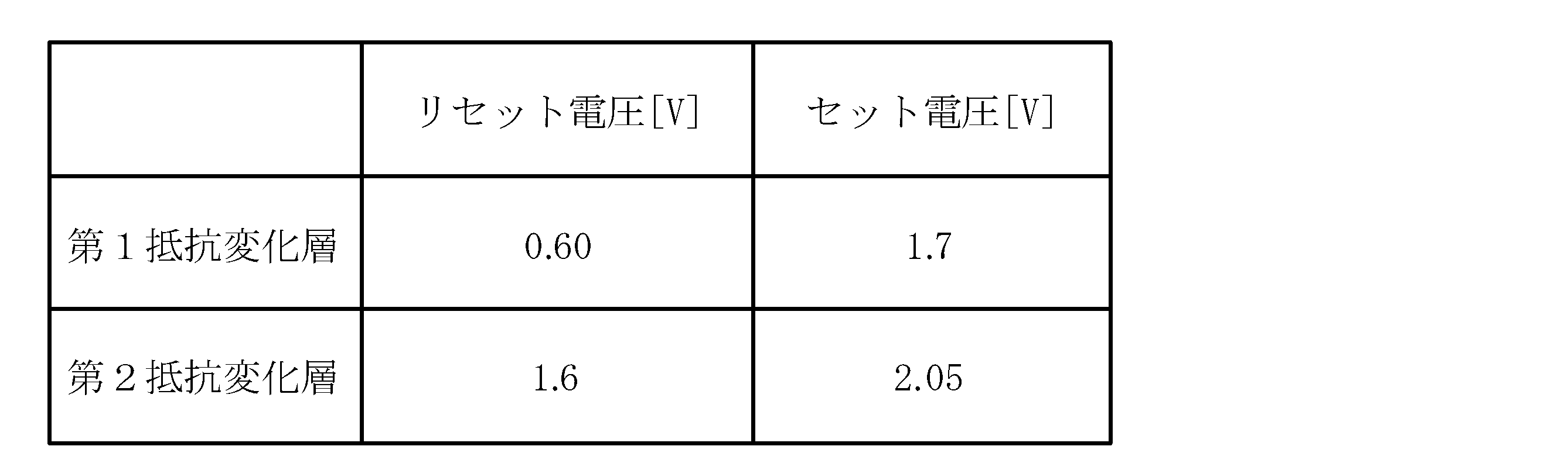
このように、本実施例の抵抗変化素子310bにおいては、第1抵抗変化層12A1と第2抵抗変化層12A2のそれぞれでリセット電圧とセット電圧が異なり、その結果、4つの抵抗状態を遷移するしきい値電圧が存在し、これにより、4値の異なる状態を有する多値メモリとして使用できる。
本実施例においては、第1及び第2抵抗変化層12A1及び12A2の厚さが、20nmと50nmとの組み合わせである場合を示したが、これらは5nm以上、50nm以下の範囲で好適であり、これにより、本実施形態に係る抵抗変化素子を用いた情報記録再生装置の特性を良好にすることができる。
(実施例3)
本実施形態に係る第3の実施例の抵抗変化素子(310c)では、第1抵抗変化層12A1には、厚さが30nmで、微結晶グラファイトとアモルファスカーボンの1:1の混合体が用いられる。第2抵抗変化層12A2には、厚さが30nmで、微結晶グラファイトとアモルファスカーボンの2:1の混合体が用いられる。下部電極11及び上部電極13Aには共にTiNが用いられる。微結晶グラファイトとアモルファスカーボンの混合体同士は、例えば1000℃以上など、通常の使用環境にて経験し得ない温度まで加熱する場合を除いては、ほとんど反応することは無く、その状態が保持される。
本実施形態に係る第3の実施例の抵抗変化素子(310c)では、第1抵抗変化層12A1には、厚さが30nmで、微結晶グラファイトとアモルファスカーボンの1:1の混合体が用いられる。第2抵抗変化層12A2には、厚さが30nmで、微結晶グラファイトとアモルファスカーボンの2:1の混合体が用いられる。下部電極11及び上部電極13Aには共にTiNが用いられる。微結晶グラファイトとアモルファスカーボンの混合体同士は、例えば1000℃以上など、通常の使用環境にて経験し得ない温度まで加熱する場合を除いては、ほとんど反応することは無く、その状態が保持される。
本実施例の抵抗変化素子310cも図7に例示したのと同様に、異なる4つの抵抗状態を有する電圧-電流特性を示した。これにより、本実施例の抵抗変化素子310cも4値の異なる抵抗状態を有する多値メモリとして使用できる。
そして、その結果から第1抵抗変化層12A1及び第2抵抗変化層12A2それぞれのリセット電圧及びセット電圧を求めた。その結果を表3に示す。
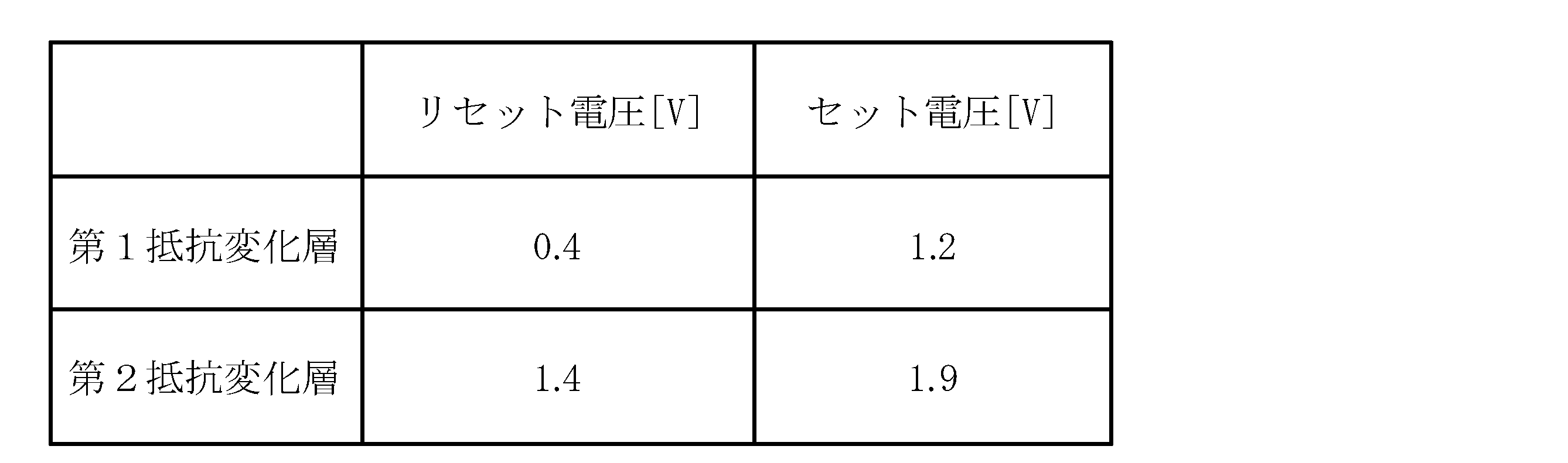
このように、本実施例の抵抗変化素子310cにおいては、第1抵抗変化層12A1と第2抵抗変化層12A2のそれぞれでリセット電圧とセット電圧が異なり、その結果、4つの抵抗状態を遷移するしきい値電圧が存在し、これにより、4値の異なる状態を有する多値メモリとして使用できる。
本実施例においては、第1及び第2抵抗変化層12A1及び12A2の厚さが、30nmと30nmとの組み合わせである場合を示したが、これらは5nm以上、50nm以下の範囲で好適であり、これにより、本実施形態に係る抵抗変化素子を用いた情報記録再生装置の特性を良好にすることができる。
なお、微結晶グラファイトとアモルファスカーボンの混合体において、その混合比はさまざまな方法にて測定することができる。例えば、ラマン分光により、D-バンドとG-バンドとのピークの比、もしくは面積強度の比を比較することにより、断面TEMの探察により、電子スピン共鳴(ESR)により、X線光電子分光法(XPS)により、もしくは電子線エネルギー損失分光法(EELS)などにより求めることができる。また、電気抵抗率の温度変化を測定することにより、その電気抵抗率の絶対値と温度係数とからも、微結晶グラファイトとアモルファスカーボンとの混合比を見積もることができる。
微結晶グラファイトとアモルファスカーボンの混合体の電気抵抗率は、10-4Ωcmから102Ωcmの間で可変させた。微結晶グラファイトとアモルファスカーボンの混合体の電気抵抗率は、微結晶グラファイトとアモルファスカーボンの混合比のみに依存するのではなく、微結晶グラファイトの結晶粒径、およびその黒鉛化度にも依存する。微結晶グラファイトの結晶粒径は、いわゆる面内方向とc軸方向の違いでも電気抵抗率への寄与が異なる。一般的にはグラファイトの面内方向への電気抵抗率は、c軸方向のそれと比較すると低い。そのため、面内方向の結晶粒径Laが大きく、その方向への電流のパスが多い場合には、電気抵抗率は下がる傾向にある。一方で、面内方向の結晶粒径があまり成長していないが、c軸方向への積層構造は保たれ、c軸方向の結晶粒径Lcとしては大きい場合には、この方向に電流のパスが多い場合でも物質としての電気抵抗率はそれほど下がらない。
微結晶グラファイトの結晶粒径としては、5nm以下、より好適には2nm以下が望ましい。
微結晶グラファイトとアモルファス・カーボンの混合体の製造方法としては、炭化水素系、例えばCH4、C3H6などのガスを反応ガスに用いるCVD法、もしくはグラファイト(黒鉛)のスパッタリング・ターゲットを用いたスパッタ法などが好適はである。これらの成膜条件を可変させることで、混合体の組織(微結晶グラファイトとアモルファスカーボンの比や結晶構造等)、電気抵抗率を可変することができる。
特に成膜時の温度に敏感であり、400℃、500℃、600℃と温度を上げてくほど、グラファイト成分が多くなる。一方で成膜速度が速い場合には、グラファイト成分は多くなり難い。CVD法を用いる場合には、膜中に反応ガス成分の水素が残留することがあるが、その量は15原子パーセント(原子百分率)程度まで及ぶことも珍しくない。この場合でも本発明の趣旨を逸脱するもではない。
また、グラファイトのその結晶構造の異方性から、グラファイトの層(2次元グラファイト、もしくはグラフェンなどとも呼ばれる)と層の間に様々な原子、分子を含有できる。これらはグラファイト層間化合物(GIC)として知られている。上記の水素および以下に述べる窒素、ボロン(B)等の成分以外にも添加することが可能である。いわゆる、炭素はグラファイトやアモルファスカーボン(無定形炭素)以外も、ダイヤモンド、またはダインモンド・ライク・カーボン(DLC)、フラーレン、カーボン・ナノ・チューブ(CNT)など様々な形態をとることができる。これらが微量含まれていても本発明の範囲を逸脱するものではない。
(実施例4)
本実施形態に係る第4の実施例の抵抗変化膜(310d)では、第1抵抗変化層12A1には、厚さが0nmで、微結晶グラファイトとアモルファス・カーボンの1:1の混合体が用いられる。第2抵抗変化層12A2には、厚さが30nmで、窒素が2原子パーセント添加された微結晶グラファイトとアモルファス・カーボンの1:1の混合体が用いられる。下部電極11及び上部電極13Aには共にTiNが用いられる。
本実施形態に係る第4の実施例の抵抗変化膜(310d)では、第1抵抗変化層12A1には、厚さが0nmで、微結晶グラファイトとアモルファス・カーボンの1:1の混合体が用いられる。第2抵抗変化層12A2には、厚さが30nmで、窒素が2原子パーセント添加された微結晶グラファイトとアモルファス・カーボンの1:1の混合体が用いられる。下部電極11及び上部電極13Aには共にTiNが用いられる。
本実施例の抵抗変化膜310dも図7に例示したのと同様に、異なる4つの抵抗状態を有する電圧-電流特性を示した。これにより、本実施例の抵抗変化素子310dも4値の異なる抵抗状態を有する多値メモリとして使用できる。
そして、その結果から第1抵抗変化層12A1及び第2抵抗変化層12A2それぞれのリセット電圧及びセット電圧を求めた。その結果を表4に示す。
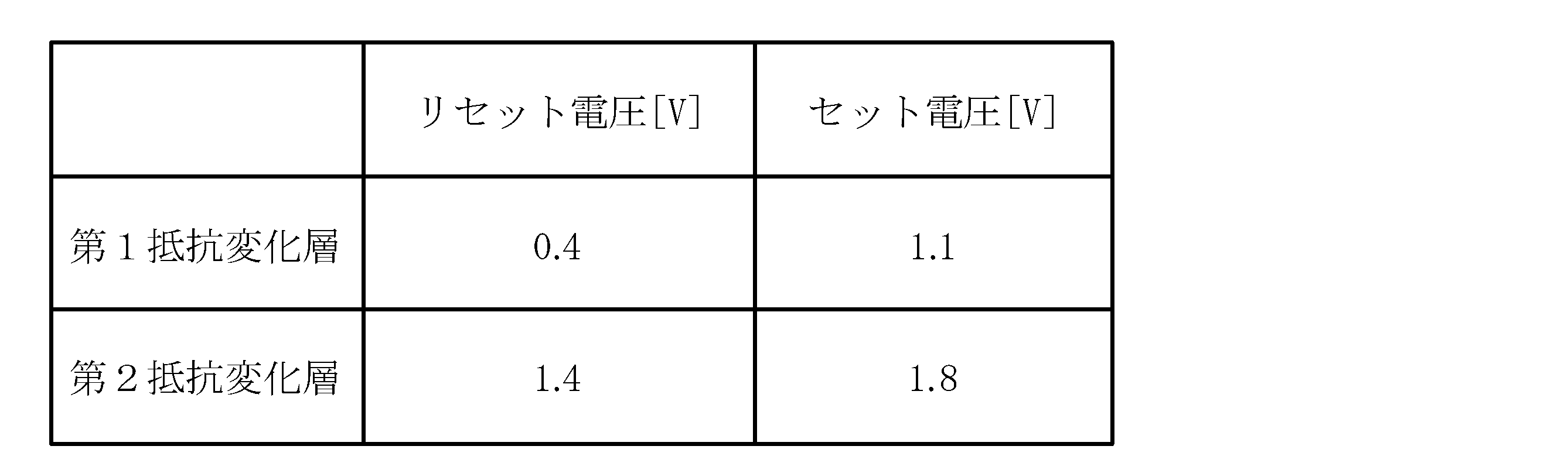
このように、本実施例の抵抗変化素子310dにおいては、第1抵抗変化層12A1と第2抵抗変化層12A2のそれぞれでリセット電圧とセット電圧が異なり、その結果、4つの抵抗状態を遷移するしきい値電圧が存在し、これにより、4値の異なる状態を有する多値メモリとして使用できる。
本実施例においては、第1及び第2抵抗変化層12A1及び12A2の厚さが、40nmと30nmとの組み合わせである場合を示したが、これらは5nm以上、50nm以下の範囲で好適であり、これにより、本実施形態に係る抵抗変化素子を用いた情報記録再生装置の特性を良好にすることができる。
(実施例5)
本実施形態に係る第5の実施例の抵抗変化膜(310e)では、第1抵抗変化層12A1には、厚さが40nmで、微結晶グラファイトとアモルファスカーボンの1:1の混合体が用いられる。第2抵抗変化層12A2には、厚さが30nmで、窒素が2原子パーセントで添加された微結晶グラファイトとアモルファスカーボンの1:1の混合体が用いられる。下部電極11及び上部電極13Aには共にTiNが用いられる。
本実施形態に係る第5の実施例の抵抗変化膜(310e)では、第1抵抗変化層12A1には、厚さが40nmで、微結晶グラファイトとアモルファスカーボンの1:1の混合体が用いられる。第2抵抗変化層12A2には、厚さが30nmで、窒素が2原子パーセントで添加された微結晶グラファイトとアモルファスカーボンの1:1の混合体が用いられる。下部電極11及び上部電極13Aには共にTiNが用いられる。
本実施例の抵抗変化膜310eも図7に例示したのと同様に、異なる4つの抵抗状態を有する電圧-電流特性を示した。これにより、本実施例の抵抗変化素子310eも4値の異なる抵抗状態を有する多値メモリとして使用できる。
そして、その結果から第1抵抗変化層12A1及び第2抵抗変化層12A2それぞれのリセット電圧及びセット電圧を求めた。その結果を表5に示す。
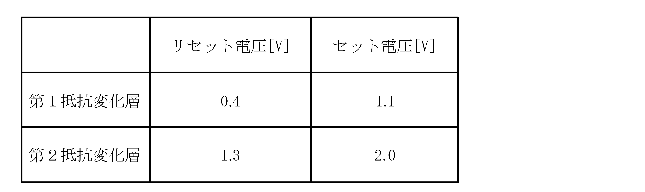
このように、本実施例の抵抗変化素子310eにおいては、第1抵抗変化層12A1と第2抵抗変化層12A2のそれぞれでリセット電圧とセット電圧が異なり、その結果、4つの抵抗状態を遷移するしきい値電圧が存在し、これにより、4値の異なる状態を有する多値メモリとして使用できる。
本実施例においては、第1及び第2抵抗変化層12A1及び12A2の厚さが、40nmと30nmとの組み合わせである場合を示したが、これらは5nm以上、50nm以下の範囲で好適であり、これにより、本実施形態に係る抵抗変化素子を用いた情報記録再生装置の特性を良好にすることができる。
(実施例6)
本実施形態に係る第6の実施例の抵抗変化膜(310f)では、第1抵抗変化層12A1には、厚さが40nmで、微結晶グラファイトとアモルファスカーボンの1:1の混合体が用いられる。第2抵抗変化層12A2には、厚さが40nmで、ボロン(B)が3原子パーセントで添加された微結晶グラファイトとアモルファスカーボンの2:1の混合体が用いられる。下部電極11及び上部電極13Aには、共にTiNが用いられる。
本実施形態に係る第6の実施例の抵抗変化膜(310f)では、第1抵抗変化層12A1には、厚さが40nmで、微結晶グラファイトとアモルファスカーボンの1:1の混合体が用いられる。第2抵抗変化層12A2には、厚さが40nmで、ボロン(B)が3原子パーセントで添加された微結晶グラファイトとアモルファスカーボンの2:1の混合体が用いられる。下部電極11及び上部電極13Aには、共にTiNが用いられる。
本実施例の抵抗変化膜310fも図7に例示したのと同様に、異なる4つの抵抗状態を有する電圧-電流特性を示した。これにより、本実施例の抵抗変化素子310fも4値の異なる抵抗状態を有する多値メモリとして使用できる。
そして、その結果から第1抵抗変化層12A1及び第2抵抗変化層12A2それぞれのリセット電圧及びセット電圧を求めた。その結果を表6に示す。

このように、本実施例の抵抗変化素子310fにおいては、第1抵抗変化層12A1と第2抵抗変化層12A2のそれぞれでリセット電圧とセット電圧が異なり、その結果、4つの抵抗状態を遷移するしきい値電圧が存在し、これにより、4値の異なる状態を有する多値メモリとして使用できる。
本実施例においては、第1及び第2抵抗変化層12A1及び12A2の厚さが、40nmと40nmとの組み合わせである場合を示したが、これらは5nm以上、50nm以下の範囲で好適であり、これにより、本実施形態に係る抵抗変化素子を用いた情報記録再生装置の特性を良好にすることができる。
(第1の比較例)
第1の比較例の抵抗変化素子においては、抵抗変化部12が1種類の材料で構成されている。すなわち、抵抗変化層12が、厚さ20nmのMn1.9O3のみの材料で構成される。これに以外は、第1の実施例の抵抗変化素子310aと同様である。
第1の比較例の抵抗変化素子においては、抵抗変化部12が1種類の材料で構成されている。すなわち、抵抗変化層12が、厚さ20nmのMn1.9O3のみの材料で構成される。これに以外は、第1の実施例の抵抗変化素子310aと同様である。
このような第1の比較例の抵抗変化素子においては、ユニポーラ動作時のリセット電圧は約+0.5Vであり、セット電圧は約+1.5Vであった。バイポーラ動作時のリセット電圧は約+0.5Vであり、セット電圧は約-0.5Vであったが、繰り返し通電サイクルにおける特性の安定性が悪く、どの素子も数百回程度で上記の動作ができなくなってしまった。そして、1つの抵抗変化素子に多値の情報を記録、再生することはできなかった。
(第2の実施の形態)
図8は、本発明の第2の実施形態に係る抵抗変化素子の構成を例示する模式的断面図である。
図8に表したように、本発明の第2の実施形態に係る抵抗変化素子320においては、下部電極11の上に第1抵抗変化層12A1、第2抵抗変化層12A2・・・第N抵抗変化層12ANが順次積層され、さらに最上層の第N抵抗変化層12ANの上に、上部電極13Aを積層した構造を有する。ここで、Nは2以上の整数である。
図8は、本発明の第2の実施形態に係る抵抗変化素子の構成を例示する模式的断面図である。
図8に表したように、本発明の第2の実施形態に係る抵抗変化素子320においては、下部電極11の上に第1抵抗変化層12A1、第2抵抗変化層12A2・・・第N抵抗変化層12ANが順次積層され、さらに最上層の第N抵抗変化層12ANの上に、上部電極13Aを積層した構造を有する。ここで、Nは2以上の整数である。
すなわち、抵抗変化素子320においては、抵抗変化部12が、組成が互いに異なり、電気的特性が互いに異なる複数の抵抗変化層を有する。
すなわち、第1抵抗変化層12A1、第2抵抗変化層12A2・・・第N抵抗変化層12ANは、それぞれ異なる組成で構成される。そして、第1抵抗変化層12A1、第2抵抗変化層12A2・・・第N抵抗変化層12ANは、それぞれ抵抗変化層であり、それぞれのセット電圧Vsi、セット電流Isi、及び、リセット電圧Vri、i=1~N)は、互いに異なる。
すなわち、第1抵抗変化層12A1、第2抵抗変化層12A2・・・第N抵抗変化層12ANは、それぞれ異なる組成で構成される。そして、第1抵抗変化層12A1、第2抵抗変化層12A2・・・第N抵抗変化層12ANは、それぞれ抵抗変化層であり、それぞれのセット電圧Vsi、セット電流Isi、及び、リセット電圧Vri、i=1~N)は、互いに異なる。
本実施形態に係る抵抗変化素子320は、それぞれの特性が異なるN層の抵抗変化層を有することから、2Nの異なる状態を有する。そして、例えば、最下層の第1抵抗変化層12A1の状態をLSBとし、最上層の第N抵抗変化層12ANの状態をMSBとして、Nビットのメモリセルとして機能する。
このように、本実施形態に係る抵抗変化素子320においては、抵抗変化部12が、組成異なり、電気的特性が異なる、任意の複数の抵抗変化層を有することができる。
(第3の実施の形態)
図9は、本発明の第3の実施形態に係る抵抗変化素子の構成を例示する模式的断面図である。
図9に表したように、本発明の第3の実施形態に係る抵抗変化素子330においては、第1抵抗変化層12A1と、第2抵抗変化層12A2が設けられ、それらの間に層間分離層(分離層)12C1が設けられている。これ以外は、抵抗変化素子310と同様とすることができるので説明を省略する。
図9は、本発明の第3の実施形態に係る抵抗変化素子の構成を例示する模式的断面図である。
図9に表したように、本発明の第3の実施形態に係る抵抗変化素子330においては、第1抵抗変化層12A1と、第2抵抗変化層12A2が設けられ、それらの間に層間分離層(分離層)12C1が設けられている。これ以外は、抵抗変化素子310と同様とすることができるので説明を省略する。
層間分離層12C1には、第1抵抗変化層12A1及び第2抵抗変化層12A2に用いられる在留尾とは異なる材料を用いることができる。層間分離層12C1には、例えば、各種の金属膜を用いることができる。
本実施形態に係る抵抗変化素子330においては、第1抵抗変化層12A1と第2抵抗変化層12A2との間に層間分離層12C1が設けられるので、第1抵抗変化層12A1と第1抵抗変化層12A2との間の元素の拡散を抑制することができる。これにより、耐熱性や耐環境性、そして書き換え耐久性が高くなるという効果がある。
また、抵抗変化部12の結晶性が向上し、素子間のばらつきやロット間のばらつきも大幅に低減できる。
そして、安定した書き換え動作の回数を増大させる。これは書き換え動作時に抵抗変化部12と他の層との間の元素の拡散、抵抗変化部12の内部での偏析等の原子レベルでの変化を非常に小さくするか、それぞれが相殺する方向に働かせる効果である。
このように、本実施形態に係る抵抗変化素子330によれば、多値記録を可能とし、性能が安定し、書き換え回数の高いる抵抗変化素子が提供できる。
(実施例7)
本実施形態に係る第7の実施例の抵抗変化素子330aを作製した。本実施例では、下部電極11、第1抵抗変化層12A1、第2抵抗変化層12A1及び上部電極13Aは、第2の実施例の抵抗変化素子310bと同じ構成とした。そして、第1抵抗変化層12Aと第2抵抗変化層12A2との間の層間分離層12C1として、ZnOにAlを6原子パーセント添加した膜を2nmの厚さで形成した。
本実施形態に係る第7の実施例の抵抗変化素子330aを作製した。本実施例では、下部電極11、第1抵抗変化層12A1、第2抵抗変化層12A1及び上部電極13Aは、第2の実施例の抵抗変化素子310bと同じ構成とした。そして、第1抵抗変化層12Aと第2抵抗変化層12A2との間の層間分離層12C1として、ZnOにAlを6原子パーセント添加した膜を2nmの厚さで形成した。
このようにして作製された本実施例の抵抗変化素子330aの特性は、第2の実施例の抵抗変化素子310bの第1~第4のしきい値電圧と実質的に同じである。
図10は、本発明の第3の実施形態に係る別の抵抗変化素子の構成を例示する模式的断面図である。
図10に表したように、本発明の第3の実施形態に係る別の抵抗変化素子331においては、抵抗変化部12が3つ以上の抵抗変化層を有しており、それぞれの抵抗変化層の間に、上記で説明した層間分離層が設けられている。
図10に表したように、本発明の第3の実施形態に係る別の抵抗変化素子331においては、抵抗変化部12が3つ以上の抵抗変化層を有しており、それぞれの抵抗変化層の間に、上記で説明した層間分離層が設けられている。
すなわち、抵抗変化素子311の抵抗変化部12は、第1抵抗変化層12A1、第2抵抗変化層12A2・・・第N抵抗変化層12ANが設けられ、それぞれの間に、第1層間分離層12C1、第2層間分離層12C2・・・第(N-1)層間分離層12C(N-1)が設けられている。
これにより、それぞれの抵抗変化層(の第1抵抗変化層12A1~第N抵抗変化層12AN)のそれぞれの間の元素の拡散を抑制することができる。これにより、耐熱性や耐環境性、そして書き換え耐久性が高くなるという効果がある。
また、抵抗変化部12の各層の結晶性が向上し、素子間のばらつきやロット間のばらつきも大幅に低減できる。
このように、本実施形態に係る別の抵抗変化素子331によれば、さらにビット数の高い多値記録を可能とし、性能が安定し、書き換え回数の高いる抵抗変化素子が提供できる。
(第4の実施の形態)
図11は、本発明の第4の実施形態に係る抵抗変化素子の構成を例示する模式的断面図である。
図11に表したように、本発明の第4の実施形態に係る抵抗変化素子340は、上記の抵抗変化素子330において、下部電極11と第1抵抗変化層12A1との間に、電極側分離層12C0が設けられている。
図11は、本発明の第4の実施形態に係る抵抗変化素子の構成を例示する模式的断面図である。
図11に表したように、本発明の第4の実施形態に係る抵抗変化素子340は、上記の抵抗変化素子330において、下部電極11と第1抵抗変化層12A1との間に、電極側分離層12C0が設けられている。
このように、下部電極11と第1抵抗変化層12A1との間に電極側分離層(分離層)12C0を設けることにより、下部電極11と第1抵抗変化層12A1との間の元素の拡散が防止でき、耐熱性や耐環境性、そして書き換え耐久性が高くすることができる。
なお、上記の層間分離層(第1層間分離層12C1~第N層間分離層12CN)及び電極側分離層12C0を合わせて、分離層12Cと言う。
(実施例8)
本発明の第4の実施形態の第8の実施例の抵抗変化素子340aを作製した。このとき、電極側分離層12C0には、SnO2にSb2O3を5原子パーセントで添加した材料を用いた。それ以外は、第7の実施例の抵抗変化素子330aと同様とする。
本発明の第4の実施形態の第8の実施例の抵抗変化素子340aを作製した。このとき、電極側分離層12C0には、SnO2にSb2O3を5原子パーセントで添加した材料を用いた。それ以外は、第7の実施例の抵抗変化素子330aと同様とする。
すなわち第1抵抗変化層12A2には、厚さ20nmのZn1.1Mn1.9O4を用い、第2抵抗変化層12A2には、厚さ50nmのNiOを用い、下部電極11にはTiNを用い、上部電極13AにはPtを用いる。
このような構成の抵抗変化素子340aのリセット電圧及びセット電圧は、表2と同様であり、互いに異なる。従って、実施例1~7と同様に、いわゆる多値の情報を記録、再生することができる。
(実施例9)
本発明の第4の実施形態に係る第9の実施例として各種の構成の抵抗変化素子を作製した。
すなわち、下部電極11にはTiNを用い、第1抵抗変化層12A1には、Mn3O4にメタルのMnを分散させた膜さ20nmの膜を用い、第2抵抗変化層12A2には、Mn3O4にMnO2を分散させた厚さ20nmの膜を用い、上部電極13AにはPtを用いた。この際、Mn3O4に分散させるメタルのMnの比率、及び、Mn3O4に分散させるMnO2の比率を変えた試料を作成した。
本発明の第4の実施形態に係る第9の実施例として各種の構成の抵抗変化素子を作製した。
すなわち、下部電極11にはTiNを用い、第1抵抗変化層12A1には、Mn3O4にメタルのMnを分散させた膜さ20nmの膜を用い、第2抵抗変化層12A2には、Mn3O4にMnO2を分散させた厚さ20nmの膜を用い、上部電極13AにはPtを用いた。この際、Mn3O4に分散させるメタルのMnの比率、及び、Mn3O4に分散させるMnO2の比率を変えた試料を作成した。
また、層間分離層12C1及び分離層12C0には、厚さ1nmのTiOs(1≦s≦2)とSnO2の混合膜を用いた。そして、層間分離層12C1及び分離層12C0として、ZnOとAl2O3の混合膜(ZnOにAlをドープしたものとも言える)、ZnOとGa2O3の混合膜(これはZnOにGaをドープしたものとも言える)、SnO2にNb2O5を混合した膜、SnO2にTa2O5を混合した膜、SnO2にSb2O3を混合した膜、In2O3にZnOを混合した膜、IrO2とIrとを混合した膜、RuO2とRuとを混合した膜が用いられた。
これらの第1及び第2抵抗変化層のリセット電圧及びセット電圧の測定結果を、表7に示す。
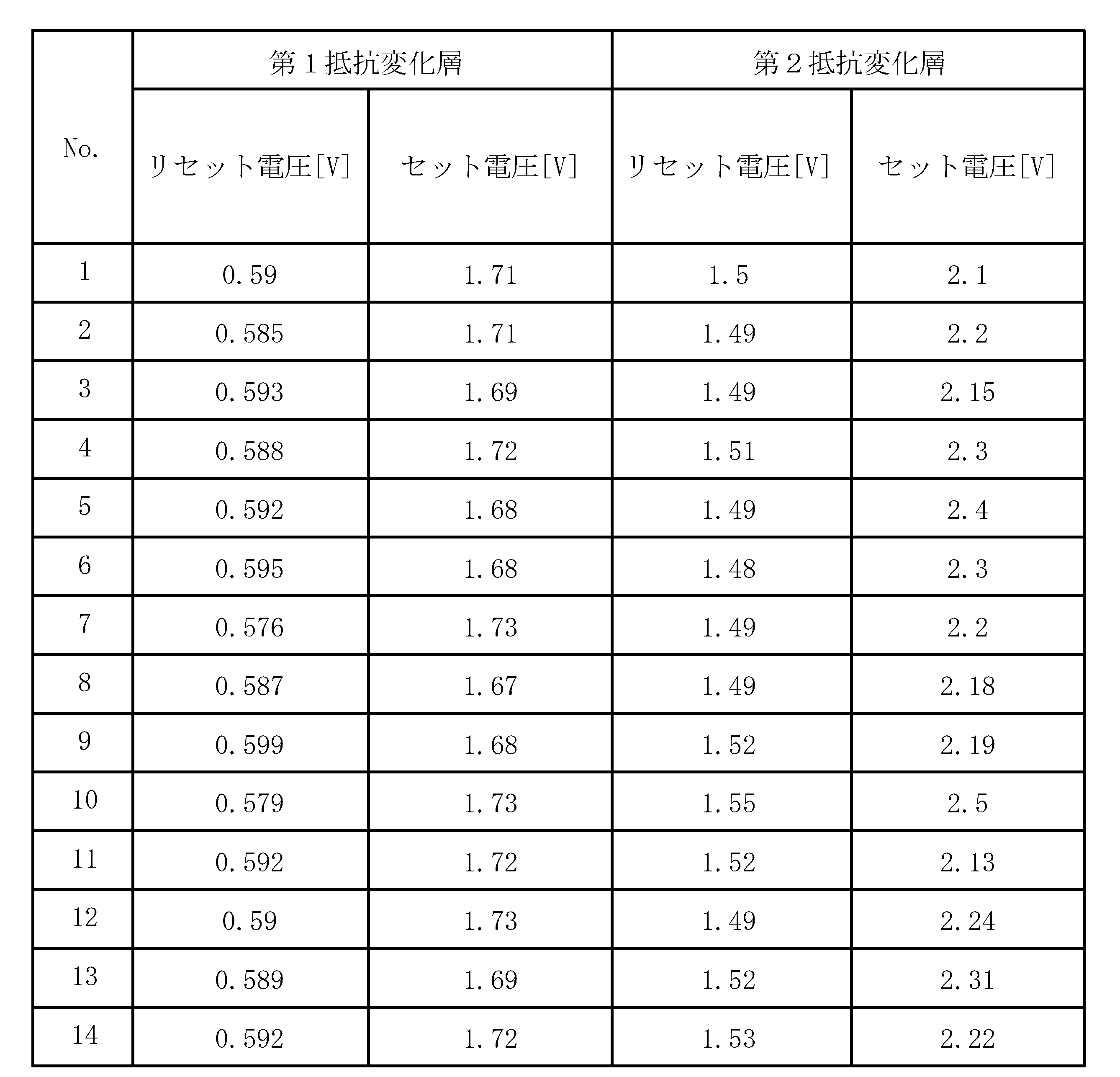
上記において、Mn3O4に分散させるメタルのMnの比率、及び、Mn3O4に分散させるMnO2の比率や分散状態等を制御し、また、用いる層間分離層12C1及び分離層12C0の材料を変えることで、抵抗変化素子の各抵抗変化層のリセット電圧及びセット電圧が制御される。また、各抵抗変化層のそれぞれの層厚も、表7に例示したようにリセット電圧及びセット電圧が所定の範囲に入るように適正な値に制御されている。
表7に示した試料1~試料14においても、例えば第1の実施例の抵抗変化素子310aと同様に、多値の記録が可能であり、再生も可能であった。
本実施例の結果からも、層間分離層12C1及び分離層12C0を用いることによって第1抵抗変化層12A1と第2抵抗変化層12A2との間、及び、第1抵抗変化層12A1と下部電極11との間における元素の拡散が比較的小さくなり、耐熱性や耐環境性、そして書き換え耐久性が高くなることが確認される。また、これと同時に、第1抵抗変化層12A1及び第2抵抗変化層12A2における結晶性が向上し、素子間のばらつき、ロット間のばらつきも大幅に低減できた。
どの抵抗変化素子も数千回以上の安定した書き換え動作が観測され、さらにそれ以上の回数の書き換えも可能であった。
これは、書き換え動作時に抵抗変化層と他の層との間の元素の拡散や、抵抗変化層の内部での偏析等の原子レベルでの変化が非常に小さいか、それぞれが相殺する方向に働くことを意味している。
そして、そのときの動作電圧の変化も、試料ごとのばらつきや測定誤差の範囲内であり、変動が非常に小さいことから、書き換え動作時に抵抗変化層と他の層との間の元素の拡散や、抵抗変化層の内部での偏析等が小さいと推定される。書き換え動作の繰り返しサイクル特性は、いずれの抵抗変化素子も1000回以上であり、データ・リテンションも良好であった。
以上説明した実施例の抵抗変化素子の評価結果から、第1抵抗変化層12A1及び第2抵抗変化層12A2のいずれか一方のリセット電圧と、いずれか他方のセット電圧と、の差は、繰り返し動作におけるばらつきや、抵抗変化素子間のばらつきや、さらには、パルス動作のときにはリンギング等のノイズ成分の大きさ等にも依存するが、発明者が実施した例の範囲では、0.1V以上が望ましい。
さらに、0.2V以上であると、さらに望ましい。
さらに、0.2V以上であると、さらに望ましい。
また、層間分離層12C1及び分離層12C0の膜厚は、0.5nm以上で効果を発揮する。すなわち、50nm以上では層間分離層12C1及び分離層12C0に接している抵抗変化層(第1抵抗変化層12A1及び第2抵抗変化層12A2)の状態を変化させてしまう。製造上の要求からも、層間分離層12C1及び分離層12C0の膜厚は、あまり厚くすることは望ましく、1~5nm程度が最も好適で、10~20nm程度であるならば、特に製造上差異は無かった。
従って、層間分離層12C1及び分離層12C0の厚さは、0.5nm以上、50nm以下が好適である。
上記の実施例では、第1抵抗変化層12A1と第2抵抗変化層12A2の厚さが20nmと50nmの組み合わせの場合を例示したが、これらは5nm以上、50nm以下の範囲で好適な情報記録再生装置とすることができる。
(第2の比較例)
実施例9と同様な構成で、抵抗変化部12の第1抵抗変化層12A1及び第2抵抗変化層12A2のリセット電圧が0.5Vで同じで、抵抗変化部12の第1抵抗変化層12A1及び第2抵抗変化層12A2のセット電圧が1.8Vで同じ構成の試料を評価した。この場合には当然ながら抵抗変化部12のリセット電圧は、約+0.5Vで、リセット電圧は、約+1.8Vであった。また、多値の情報を記録、再生することはできなかった。
実施例9と同様な構成で、抵抗変化部12の第1抵抗変化層12A1及び第2抵抗変化層12A2のリセット電圧が0.5Vで同じで、抵抗変化部12の第1抵抗変化層12A1及び第2抵抗変化層12A2のセット電圧が1.8Vで同じ構成の試料を評価した。この場合には当然ながら抵抗変化部12のリセット電圧は、約+0.5Vで、リセット電圧は、約+1.8Vであった。また、多値の情報を記録、再生することはできなかった。
以上、説明したように、第1~9の実施例のいずれにおいても、情報記録再生装置として、記録膜の特性を制御することで、多値の情報を記録、再生することができた。また、従来よりも低消費電力化を達成でき、かつサイクル特性を見ても、本実施例が格段に優れていた。
図12は、本発明の第4の実施形態に係る別の抵抗変化素子の構成を例示する模式的断面図である。
図12に表したように、本発明の第4の実施形態に係る別の抵抗変化素子341では、抵抗変化部12がN個の抵抗変化層(第1~第N抵抗変化12A1~12AN)で構成され、それぞれの抵抗変化層の間に層間分離層12C1~12C(N-1)が設けられ、抵抗変化部12と下部電極11との間に分離層12C0が設けられ、抵抗変化部12と上部電極13Aとの間に分離層12CNが設けられている。
図12に表したように、本発明の第4の実施形態に係る別の抵抗変化素子341では、抵抗変化部12がN個の抵抗変化層(第1~第N抵抗変化12A1~12AN)で構成され、それぞれの抵抗変化層の間に層間分離層12C1~12C(N-1)が設けられ、抵抗変化部12と下部電極11との間に分離層12C0が設けられ、抵抗変化部12と上部電極13Aとの間に分離層12CNが設けられている。
このように、任意のN個の抵抗変化層の間に層間分離層を設けることができる。なお、N個の抵抗変化層のそれぞれの間の全てに層間分離層を設けなくても良く、任意の箇所に設けても良い。
また、下部電極11及び上部電極13のいずれかの間に分離層を設けることができる。 ここで、第1~第Nの層間分離層12C1~12C(N-1)を総称して、層間分離層12Cという。
また分離層12C0は下部電極11及び上部電極13Aの少なくともいずれかと兼用されても良い。
また分離層12C0は下部電極11及び上部電極13Aの少なくともいずれかと兼用されても良い。
(第5の実施の形態)
図13は、本発明の第5の実施形態に係る抵抗変化素子の構成を例示する模式的断面図である。
図13に表したように、本発明の第5の実施の形態における抵抗変化素子350は、下部電極11と第1抵抗変化層12A1との間に電流制限層12Dが設けられている。
図13は、本発明の第5の実施形態に係る抵抗変化素子の構成を例示する模式的断面図である。
図13に表したように、本発明の第5の実施の形態における抵抗変化素子350は、下部電極11と第1抵抗変化層12A1との間に電流制限層12Dが設けられている。
既に説明したように、抵抗変化素子において、例えば、消去状態から第1抵抗変化層12A1のみがセット状態に変化する場合、第1抵抗変化層12A1と第2抵抗変化層12A2の両者にかかっていた電圧がほぼ第2抵抗変化層12A2のみにかかることになり、ラッシュ電流が流れる。また、その電圧が、第2抵抗変化層12A2のセット電圧より大きい場合には、第2抵抗変化層12A2も同時にリセットする場合が発生する。 そこで、本実施形態に係る抵抗変化素子350において、このようなラッシュ電流を制限するために、下部電極11と抵抗変化部12との間に、電流制限層12Dを設けている。
この電流制限層12Dには、アクティブ・デバイスであるトランジスタやダイオードも利用可能であるが、抵抗変化素子を含めた素子電体の電気抵抗が高くなるような、いわゆる抵抗層を用いることができる。
また、電流制限層12Dは、下部電極11と抵抗変化部12との間、及び、抵抗変化部12と上部電極13Aとの間、の少なくともいずれかに設けることができる。
なお、後述するように、抵抗変化素子が応用される情報記録再生装置におけるトランジスタ、ダイオード、抵抗、キャパシタを用いるドライバ回路で電流を制限することも可能である。
図14は、本発明の第5の実施形態に係る別の抵抗変化素子の構成を例示する模式的断面図である。
図14に表したように、本実施形態に係る別の抵抗変化素子351においては、抵抗変化部12が、N個の抵抗変化層(第1~第N抵抗変化12A1~12AN)で構成され、それぞれの抵抗変化層の間に層間分離層12C1~12C(N-1)が設けられ、下部電極12と第1抵抗変化層12A1との間に電流制限層12Dが設けられている。
図14に表したように、本実施形態に係る別の抵抗変化素子351においては、抵抗変化部12が、N個の抵抗変化層(第1~第N抵抗変化12A1~12AN)で構成され、それぞれの抵抗変化層の間に層間分離層12C1~12C(N-1)が設けられ、下部電極12と第1抵抗変化層12A1との間に電流制限層12Dが設けられている。
なお、電流制限層12Dは抵抗変化層12Dと上部電極13Aとの間に設けても良く、また、電流制限層12Dは、下部電極11と上部電極13Aとの間の任意の場所に設けることができ、また、任意の数の電流制限層12Dを設けることができる。
(第6の実施の形態)
図15は、本発明の第6の実施形態に係る抵抗変化素子の構成を例示する模式的断面図である。
図15に表したように、本発明の第6の実施形態に係る抵抗変化素子360は、下部電極11と第1記録素子12A1との間に、抵抗変化層の配向を制御する配向制御層11Aが設けられている。
図15は、本発明の第6の実施形態に係る抵抗変化素子の構成を例示する模式的断面図である。
図15に表したように、本発明の第6の実施形態に係る抵抗変化素子360は、下部電極11と第1記録素子12A1との間に、抵抗変化層の配向を制御する配向制御層11Aが設けられている。
この配向制御層11Aには、例えば、各種の金属と窒素との化合物を用いることができ、これにより、抵抗変化層の配向性を高め、特性の良好な抵抗変化層が再現性良く得られる。
本実施形態に係る抵抗変化素子360が応用される情報記録再生装置においては、多値の記録が行われる。この際、抵抗変化素子360には高い品質が求められ、このためには、複数の抵抗変化層の特性が安定することが非常に重要である。このとき、本実施形態に係る抵抗変化素子360において、配向制御層11Dを設けることで、抵抗変化層の品質を安定化させる。これにより、品質が高い多値記録を可能とする抵抗変化素子が抵抗できる。
(第7の実施の形態)
図16は、本発明の第7の実施形態に係る抵抗変化素子の構成を例示する模式的断面図である。
図16(a)に表したように、本発明の第7の実施形態に係る抵抗変化素子370においては、第1抵抗変化層12A1及び第2抵抗変化層12A2のそれぞれに隣接して、それぞれ第1イオン格納層12B1及び第2イオン格納層12B2が設けられている。
図16は、本発明の第7の実施形態に係る抵抗変化素子の構成を例示する模式的断面図である。
図16(a)に表したように、本発明の第7の実施形態に係る抵抗変化素子370においては、第1抵抗変化層12A1及び第2抵抗変化層12A2のそれぞれに隣接して、それぞれ第1イオン格納層12B1及び第2イオン格納層12B2が設けられている。
第1イオン格納層12B1及び第2イオン格納層12A2は、第1抵抗変化層12A1及び第2抵抗変化層12A2から排出されるイオンを格納する機能を有し、イオンの移動をより円滑化する効果を有する。また、用いる材料の工夫により、イオンの出入りによらず高い電子伝導性を常に有することができ、また、結晶構造安定性の維持を保障する効果を有することもできる。この結果、逆方向電圧印加によるディスターブ耐性を向上させることができる。
また、図16(b)に表したように、抵抗変化素子371においては、第1抵抗変化層12A1に隣接して第1イオン格納層12B1が設けられている。
また、図16(c)に表したように、抵抗変化素子372においては、第2抵抗変化層12A2に隣接して第2イオン格納層12B2が設けられている。
このように、第1抵抗変化層12A1及び第2抵抗変化層12A2の少なくともいずれかに、イオン格納層を設けても良い。
また、図16(b)に表したように、抵抗変化素子371においては、第1抵抗変化層12A1に隣接して第1イオン格納層12B1が設けられている。
また、図16(c)に表したように、抵抗変化素子372においては、第2抵抗変化層12A2に隣接して第2イオン格納層12B2が設けられている。
このように、第1抵抗変化層12A1及び第2抵抗変化層12A2の少なくともいずれかに、イオン格納層を設けても良い。
また、図16(d)に表したように、抵抗変化素子373においては、抵抗変化部12において、N個の抵抗変化層、すなわち、第1~第N抵抗変化層12A1~12ANが設けられており、第1~第N抵抗変化層12A1~12ANの少なくともいずれかのそれぞれに、第1~第Nイオン格納層12B1~12BNが設けられている。
なお、第1~第N抵抗変化層12A1~12ANを総称して抵抗変化層12Aという。また、第1~第Nイオン格納層12B1~12BNを総称してイオン格納層12Bという。
このように、本実施形態に係る抵抗変化素子370~373のように、抵抗変化部12において、抵抗変化層12Aにイオン格納層を設けることで、抵抗変化動作が安定した抵抗変化素子が提供できる。
第1イオン格納層12A1及び第2イオン格納層12A2に用いることができる材料については後述する。
以下、本発明の実施形態に係る抵抗変化素子に用いられる抵抗変化層において、抵抗の異なる複数の状態が生成される機構についての一例について説明し、あわせて、抵抗変化層や電極などに適用できる構成や材料について説明する。
図17は、本発明の実施形態に係る抵抗変化素子の一部の構成及び動作を例示する模式図である。
なお、同図は、説明を簡単にするため、1つの抵抗変化層における動作を例示しているので、下部電極11と上部電極13Aとの間に1つの抵抗変化層(抵抗変化部12)がある場合が例示されている。
なお、同図は、説明を簡単にするため、1つの抵抗変化層における動作を例示しているので、下部電極11と上部電極13Aとの間に1つの抵抗変化層(抵抗変化部12)がある場合が例示されている。
図17に表したように、記録部(抵抗変化部)12は、第1種の層81を有し、第1種の層81は、拡散イオン52(Aイオン)と、遷移元素イオン51(Mイオン)と、陰イオン61(Xイオン)を有する第1種の化合物71からなる。
すなわち、抵抗変化層12Aに用いられる化合物は、例えば、少なくとも2種類の陽イオン元素を有する複合化合物から構成され、前記陽イオン元素の少なくとも1種類は、電子が不完全に満たされたd軌道を有する遷移元素であり、少なくとも1種類の遷移元素を有する。
より具体的には、記録層12Aに用いられる化合物は、少なくとも2種類の陽イオン元素を有する複合化合物から構成され、前記陽イオン元素の少なくとも1種類は、電子が不完全に満たされたd軌道を有する遷移元素を含む導電性酸化物とすることができる。
以下では、初期状態を高抵抗状態HRとし、記録部12に形成される電位勾配により記録部12の状態を変化させ、記録部12に伝導性を持たせて低抵抗状態LRとすることにより行う情報記録を行う場合の機構の一例を説明する。
まず、セット動作SOにおいては、例えば、上部電極13Aの電位が下部電極11の電位よりも相対的に低い状態を作る。すなわち、例えば、下部電極11を固定電位(例えば、接地電位)とし、上部電極13Aに負の電位を与える。
このとき、抵抗変化部12内の拡散イオン52の一部が上部電極(陰極)13Aの側に移動し、記録部(結晶)12内の拡散イオン52が陰イオン61に対して相対的に減少する。上部電極13Aの側に移動した拡散イオン52は、上部電極13Aから電子を受け取り、メタル(A金属52m)として析出し、メタル層14を形成する。
記録部12の内部では、陰イオン61が過剰となり、結果的に、記録部12内の遷移元素イオン51の価数を上昇させる。つまり、記録部12は、キャリアの注入により電子伝導性を有するようになるため、セット状態となり、情報記録が完了する。
情報再生に関しては、電流パルスを記録部12に流し、記録部12の抵抗値を検出することにより行う。ただし、電流パルスは、記録部12を構成する材料が状態変化を起こさない程度の微小な値とされる。
以上の過程は、一種の電気分解であり、下部電極(陽極)11の側では、電気化学的酸化により酸化剤が生じ、上部電極(陰極)13Aの側では、電気化学的還元により還元剤が生じた、と考えることができる。
このため、情報記録の状態(低抵抗状態LR)を初期状態(高抵抗状態HR)に戻すには、例えば、記録部12を大電流パルスによりジュール加熱して、記録部12の酸化還元反応を促進させれば良い。すなわち、大電流パルスの遮断後の残留熱により記録部12は、高抵抗状態HRに戻る(リセット動作RO)。
なお、この動作機構を用いた場合、室温でリセット動作ROが生じないように、リテンション時間が十分長く確保される。そして、リセット動作ROの消費電力は小さくされる。
これに対し、拡散イオン52の配位数を小さく(理想的には2以下に)する、もしくは、価数を2以上にする、又は、陰イオン61の価数を上げる(理想的には3以上にする)ことで、リテンション時間を十分小さくできる。
また、結晶破壊を引き起こさないために拡散イオン52の価数を2以下にし、それと共に、記録部(結晶)12内を移動する拡散イオン52の移動パスを数多く有する材料を用いることで上記の消費電力を十分に小さくすることができる。
そのような特性を記録部12に持たせるためには、以下において述べるような元素及び結晶構造、そして、イオン格納層を採用すれば良い。
記録部(抵抗変化部)12の各層(各抵抗変化層)には、以下の(1)~(3)で表される材料の少なくともいずれかを用いることができる。
(1)AxMyX4(0.1≦x≦2.2、1.8≦y≦2)
ここで、Aは、Na、K、Rb、Be、Mg、Ca、Sr、Ba、Al、Ga、Mn、Fe、Co、Ni、Cu、Zn、Ge、Ag、Au、Cd、Sn、Sb、Pt、Pd、Hg、Tl、Pb及びBiよりなる群から選択された少なくともいずれかを含む元素であり、Mは、Al、Ga、Ti、Ge、Sn、V、Cr、Mn、Fe、Co、Ni、Nb、Ta、Mo、W、Ru及びRhよりなる群から選択された少なくともいずれかを含む元素であり、前記XはO及びNよりなる群から選択された少なくともいずれかを含む元素であり、AとMとは互いに異なる元素である。
ここで、Aは、Na、K、Rb、Be、Mg、Ca、Sr、Ba、Al、Ga、Mn、Fe、Co、Ni、Cu、Zn、Ge、Ag、Au、Cd、Sn、Sb、Pt、Pd、Hg、Tl、Pb及びBiよりなる群から選択された少なくともいずれかを含む元素であり、Mは、Al、Ga、Ti、Ge、Sn、V、Cr、Mn、Fe、Co、Ni、Nb、Ta、Mo、W、Ru及びRhよりなる群から選択された少なくともいずれかを含む元素であり、前記XはO及びNよりなる群から選択された少なくともいずれかを含む元素であり、AとMとは互いに異なる元素である。
(2)AxMyX3(0.5≦x≦1.1、0.9≦y≦1)
ここで、Aは、Na、K、Rb、Be、Mg、Ca、Sr、Ba、Al、Ga、Mn、Fe、Co、Ni、Cu、Zn、Ge、Ag、Au、Cd、Sn、Sb、Pt、Pd、Hg、Tl、Pb及びBiよりなる群から選択された少なくともいずれかを含む元素であり、Mは、Al、Ga、Ti、Ge、Sn、V、Cr、Mn、Fe、Co、Ni、Nb、Ta、Mo、W、Ru及びRhよりなる群から選択された少なくともいずれかを含む元素であり、Xは、O及びNよりなる群から選択された少なくともいずれかを含む元素であり、AとMとは互いに異なる元素である。
ここで、Aは、Na、K、Rb、Be、Mg、Ca、Sr、Ba、Al、Ga、Mn、Fe、Co、Ni、Cu、Zn、Ge、Ag、Au、Cd、Sn、Sb、Pt、Pd、Hg、Tl、Pb及びBiよりなる群から選択された少なくともいずれかを含む元素であり、Mは、Al、Ga、Ti、Ge、Sn、V、Cr、Mn、Fe、Co、Ni、Nb、Ta、Mo、W、Ru及びRhよりなる群から選択された少なくともいずれかを含む元素であり、Xは、O及びNよりなる群から選択された少なくともいずれかを含む元素であり、AとMとは互いに異なる元素である。
(3)AxMyX4(0.5≦x≦1.1、0.9≦y≦1)
ここで、Aは、Mg、Ca、Sr、Al、Ga、Sb、Ti、V、Cr、Mn、Fe、Co、Rh、In、Sb、Tl、Pb及びBiよりなる群から選択された少なくともいずれかを含む元素であり、Mは、Al、Ga、Ti、Ge、Sn、V、Nb、Ta、Cr、Mn、Mo、W、Ir及びOsよりなる群から選択された少なくともいずれかを含む元素であり、Xは、O及びNよりなる群から選択された少なくともいずれかを含む元素であり、AとMとは互いに異なる元素である。
ここで、Aは、Mg、Ca、Sr、Al、Ga、Sb、Ti、V、Cr、Mn、Fe、Co、Rh、In、Sb、Tl、Pb及びBiよりなる群から選択された少なくともいずれかを含む元素であり、Mは、Al、Ga、Ti、Ge、Sn、V、Nb、Ta、Cr、Mn、Mo、W、Ir及びOsよりなる群から選択された少なくともいずれかを含む元素であり、Xは、O及びNよりなる群から選択された少なくともいずれかを含む元素であり、AとMとは互いに異なる元素である。
また、記録部(抵抗変化部)12の各層(各抵抗変化層)には、コランダム構造、ルチル構造、スピネル構造、ラムスデライト構造、アナターゼ構造、ホランダイト構造、ブルッカイト構造、パイロルース構造、NaC構造、プロベスカイト構造、イルメナイト構造、ウルフラマイト構造よりなる郡から選択されたいずれかの構造を有する結晶構造を有することができる。
そして、第1~第7の実施形態に係る抵抗変化素子の複数の抵抗変化層12A(第1抵抗変化層12A1~第N抵抗変化層12AN)のそれぞれにおいては、上記に例示した材料及び構成のうち、異なる材料、異なる成分比、及び、異なる構成の少なくともいずれかが用いられる。これにより、複数の抵抗変化層12A(第1抵抗変化層12A1~第N抵抗変化層12AN)のそれぞれにおいて、セット電圧及びリセット電圧の少なくともいずれかを異ならせることができる。
また、記録部12に、第7の実施形態で説明したイオン格納層12Bを設けることができる。
図18は、本発明の実施形態に係る抵抗変化素子の一部の構成及び動作を例示する模式的断面図である。
すなわち、同図は、抵抗変化素子におけるイオン格納層12Bの作用を模式的に例示したものであり、抵抗変化層12Aが一層で、イオン格納層12Bが一層として模式的に描かれている。
図18は、本発明の実施形態に係る抵抗変化素子の一部の構成及び動作を例示する模式的断面図である。
すなわち、同図は、抵抗変化素子におけるイオン格納層12Bの作用を模式的に例示したものであり、抵抗変化層12Aが一層で、イオン格納層12Bが一層として模式的に描かれている。
図18に表したように、記録部12においては、抵抗変化層12Aに隣接して、イオン格納層12Bが設けられている。イオン格納層12Bは、第2種の層82からなり、第2種の層82は、遷移金属イオン53と陰イオン61とを含み、さらに、抵抗変化層12Aの移動するAイオン52を格納可能な空隙サイトαを有する第2種の化合物72からなる。これにより、セット動作(SO)において、抵抗変化層12Aから移動してきたAイオン52を、イオン格納層12Bの空隙サイトαに格納する。そして、リセット動作ROにおいては、イオン格納層12Bの空隙サイとαに格納されていたAイオン52を放出し、Aイオン52は、抵抗変化層12Aに再び移動する。このように、イオン格納層12Bを設けることで、2つの状態のそれぞれを安定化させることができ、この結果、これらの2つの状態に対応する高抵抗状態と低抵抗状態を安定して再現性良く発現させることができる。
図19は、本発明の実施形態に係る別の抵抗変化素子の一部の構成及び動作を例示する模式的断面図である。
図19に表したように、本発明の実施形態に係る別の抵抗変化素子においては、複数の抵抗変化層(第1抵抗変化層12A1~第N抵抗変化層12A2)の少なくともいずれかが、イオン格納層(第1イオン格納層12B1~第Nイオン格納層12BN)を有す。この場合も同様に、複数の抵抗変化層12AのそれぞれのAイオン52を、それに隣接するイオン格納層12Bの空隙サイトαに格納することができ、高抵抗状態と低抵抗状態の2つの状態を安定して発現させることができる。
図19に表したように、本発明の実施形態に係る別の抵抗変化素子においては、複数の抵抗変化層(第1抵抗変化層12A1~第N抵抗変化層12A2)の少なくともいずれかが、イオン格納層(第1イオン格納層12B1~第Nイオン格納層12BN)を有す。この場合も同様に、複数の抵抗変化層12AのそれぞれのAイオン52を、それに隣接するイオン格納層12Bの空隙サイトαに格納することができ、高抵抗状態と低抵抗状態の2つの状態を安定して発現させることができる。
イオン格納層12Bには、例えば導電性酸化物を用いるものが望ましい。そして、この導電性酸化物層の抵抗率は、抵抗変化層12Aの抵抗率以下であり、10-1Ωcm以下であることが望ましい。
イオン格納層12Bは、空隙サイトαを持つ点に特徴を有する。ただし、空隙サイトαは抵抗変化層12Aから移動してきた陽イオンが一部埋めていても良い。イオン格納層12Bには以下の(4)~(6)で表される材料の少なくともいずれかを用いることができる。
(4)A1-xMxX2-u
ただし、Aは、Ti、Zr、Hf及びSnよりなる群から選択される少なくとも1種類の元素であり、Mは、V、Nb、Ta、Cr、Mo、W、As、Sb及びBiよりなる群から選択される少なくとも1種類の元素であり、Xは、O、N及びFよりなる群からから選択される少なくとも1種類の元素であり、AとMとは異なる元素であり、0.001<x≦0.2、0≦u<0.2である。
ただし、Aは、Ti、Zr、Hf及びSnよりなる群から選択される少なくとも1種類の元素であり、Mは、V、Nb、Ta、Cr、Mo、W、As、Sb及びBiよりなる群から選択される少なくとも1種類の元素であり、Xは、O、N及びFよりなる群からから選択される少なくとも1種類の元素であり、AとMとは異なる元素であり、0.001<x≦0.2、0≦u<0.2である。
(5)A2-xMxX3-u
ただし、Aは、V、Nb、Ta、Cr、Mo、W、Mn、Fe、Co、Ga及びInよりなる群から選択される少なくとも1種類の元素であり、Mは、Ti、Zr、Hf、Sn、V、Nb、Ta、As、Sb、Bi、Cr、Mo及びWよりなる群から選択される少なくとも1種類の元素であり、Xは、O、N及びFよりなる群から選択される少なくとも1種類の元素であり、AとMとは異なる元素であり、0.001<x≦0.2、0≦u<0.3である。
ただし、Aは、V、Nb、Ta、Cr、Mo、W、Mn、Fe、Co、Ga及びInよりなる群から選択される少なくとも1種類の元素であり、Mは、Ti、Zr、Hf、Sn、V、Nb、Ta、As、Sb、Bi、Cr、Mo及びWよりなる群から選択される少なくとも1種類の元素であり、Xは、O、N及びFよりなる群から選択される少なくとも1種類の元素であり、AとMとは異なる元素であり、0.001<x≦0.2、0≦u<0.3である。
(6)A2-xMxX5-u
ただし、Aは、V、Nb及びTaよりなる群から選択される少なくとも1種類の元素であり、Mは、Cr、Mo及びWよりなる群から選択される少なくとも1種類の元素であり、Xは、O、N及びFよりなる群から選択される少なくとも1種類の元素であり、AとMとは異なる元素であり、0.001<x≦0.2、0≦u<0.5である。
ただし、Aは、V、Nb及びTaよりなる群から選択される少なくとも1種類の元素であり、Mは、Cr、Mo及びWよりなる群から選択される少なくとも1種類の元素であり、Xは、O、N及びFよりなる群から選択される少なくとも1種類の元素であり、AとMとは異なる元素であり、0.001<x≦0.2、0≦u<0.5である。
これらの材料は、抵抗変化層12Aから排出されるイオンを格納する機能を有するため、イオンの移動をより円滑化する効果を有すると共に、x>0.001に組成範囲を限定することでイオンの出入りによらず10S/cm以上の電子伝導性を常に有し、またx≦0.2と組成範囲を限定することで結晶構造安定性の維持を保障する効果を有する。
この結果、逆方向電圧印加によるディスターブ耐性の向上を実現することができる。
この結果、逆方向電圧印加によるディスターブ耐性の向上を実現することができる。
一方、下部電極11には以下の材料を用いることができる。
すなわち、セット動作SO後の下部電極(陽極)11の側には酸化剤が生じるため、下部電極11には、酸化され難い材料(例えば、電気伝導性窒化物、電気伝導性酸化物など)から構成するのが好ましい。
また、電極層11には、イオン伝導性を有しない材料を用いるのが良い。
すなわち、セット動作SO後の下部電極(陽極)11の側には酸化剤が生じるため、下部電極11には、酸化され難い材料(例えば、電気伝導性窒化物、電気伝導性酸化物など)から構成するのが好ましい。
また、電極層11には、イオン伝導性を有しない材料を用いるのが良い。
そのような材料としては、以下に示されるものがあり、その中でも、電気伝導率の良さなどを加味した総合的性能の点から、LaNiO3は、最も好ましい材料ということができる。
下部電極11には、以下の(7)~(10)で表される材料の少なくともいずれかを用いることができる。
(7)MN
ただし、Mは、Ti、Zr、Hf、V、Nb及びTaよりなる群から選択される少なくとも1種類の元素を含み、Nは、窒素である。
ただし、Mは、Ti、Zr、Hf、V、Nb及びTaよりなる群から選択される少なくとも1種類の元素を含み、Nは、窒素である。
(8)MOx
ただし、Mは、Ti、V、Cr、Mn、Fe、Co、Ni、Cu、Zr、Nb、Mo、Ru、Rh、Pd、Ag、Hf、Ta、W、Re、Ir、Os及びPtよりなる群から選択される少なくとも1種類の元素を含み、モル比xは、1≦x≦4を満たすものとする。
ただし、Mは、Ti、V、Cr、Mn、Fe、Co、Ni、Cu、Zr、Nb、Mo、Ru、Rh、Pd、Ag、Hf、Ta、W、Re、Ir、Os及びPtよりなる群から選択される少なくとも1種類の元素を含み、モル比xは、1≦x≦4を満たすものとする。
(9)AMO3
ただし、Aは、La、K、Ca、Sr、Ba及びLn(Lanthanide)よりなる群から選択される少なくとも1種類の元素を含み、 Mは、Ti、V、Cr、Mn、Fe、Co、Ni、Cu、Zr、Nb、Mo、Ru、Rh、Pd、Ag、Hf、Ta、W、Re、Ir、Os及びPtよりなる群から選択される少なくとも1種類の元素を含み、Oは、酸素である。
ただし、Aは、La、K、Ca、Sr、Ba及びLn(Lanthanide)よりなる群から選択される少なくとも1種類の元素を含み、 Mは、Ti、V、Cr、Mn、Fe、Co、Ni、Cu、Zr、Nb、Mo、Ru、Rh、Pd、Ag、Hf、Ta、W、Re、Ir、Os及びPtよりなる群から選択される少なくとも1種類の元素を含み、Oは、酸素である。
(10)B2MO4
ただし、Bは、K、Ca、Sr、Ba及びLn(Lanthanide)よりなる群から選択される少なくとも1種類の元素を含み、Mは、Ti、V、Cr、Mn、Fe、Co、Ni、Cu、Zr、Nb、Mo、Ru、Rh、Pd、Ag、Hf、Ta、W、Re、Ir、Os及びPtよりなる群から選択される少なくとも1種類の元素を含み、 Oは、酸素である。
ただし、Bは、K、Ca、Sr、Ba及びLn(Lanthanide)よりなる群から選択される少なくとも1種類の元素を含み、Mは、Ti、V、Cr、Mn、Fe、Co、Ni、Cu、Zr、Nb、Mo、Ru、Rh、Pd、Ag、Hf、Ta、W、Re、Ir、Os及びPtよりなる群から選択される少なくとも1種類の元素を含み、 Oは、酸素である。
また、下部電極11には、Au、Ru、Ir及びW等の金属を用いることもできる。
一方、上部電極13Aには以下の材料を用いることができる。
すなわち、セット動作SO後の上部電極(陰極)13Aの側には還元剤が生じるため、上部電極13Aとしては、記録部12が大気と反応することを防止する機能を持っていることが好ましい。
そのような材料としては、例えば、アモルファスカーボン、ダイヤモンドライクカーボン、SnO2などの半導体がある。
すなわち、セット動作SO後の上部電極(陰極)13Aの側には還元剤が生じるため、上部電極13Aとしては、記録部12が大気と反応することを防止する機能を持っていることが好ましい。
そのような材料としては、例えば、アモルファスカーボン、ダイヤモンドライクカーボン、SnO2などの半導体がある。
また、上部電極13Aには、Au、Ru、Ir及びW等の金属も用いることができる。
上部電極13Aは、記録部12を保護する保護層として機能させても良いし、上部電極13Aの代わりに保護層を設けても良い。この場合、保護層は、絶縁体でも良いし、導電体でも良い。
なお、下部電極11と上部電極13Aとは互いに入れ替えが可能であり、上記の下部電極11と上部電極13Aに用いる事が出来る材料は互いに入れ替えが可能である。
例えば、下部電極11及び上部電極13Aには、各実施例で説明した材料の他に、TiSiN、TaN、TaSiN、WNを用いることができる。また、SiN、TiC、TaC、SiCも好適であり、これらを混合することも好適である。また、Au、Ru、Ir、W等の金属も下部電極11及び上部電極13Aに用いることができる。
また、下部電極11及び上部電極13Aには、Ti-N、Ti-Si-N、Ta-N、Ta-Si-N、Si-N、Ti-N、Ta-C、Si-C及びW-Nよりなる群から選ばれた少なくともいずれかの窒化物、炭化物、酸化物、及び、窒化物と炭化物と酸化物とのうちの少なくとも2以上からなる混合体、の少なくともいずれかを用いることができる。すなわち、前記群から選ばれた少なくとも1種の窒化物、炭化物、酸化物、窒化物と酸化物との混合体、窒化物と炭化物との混合体、酸化物と炭化物との混合体、または、窒化物と炭化物と酸化物との混合体のいずれかを用いることができる。
一方、分離層12C、すなわち、層間分離層12C(第1層間分離層12C1~第N分離層12CN)及び分離層12C0は、Ti-N、Ti-Si-N、Ta-N、Ta-Si-N、Si-N、Ti-C、Ta-C、Si-C及びW-Nよりなる群から選択された少なくともいずれかの窒化物、炭化物、酸化物、及び、窒化物と炭化物と酸化物とのうち少なくとも2つ以上からなる混合体、の少なくともいずれかを含むことができる。すなわち、前記群から選ばれた少なくとも1種の窒化物、炭化物、酸化物、窒化物と酸化物との混合体、窒化物と炭化物との混合体、酸化物と炭化物との混合体、窒化物と炭化物と酸化物との混合体のいずれかを含むことができる。
また、分離層12Cは、ZnO、SnO2、In2O3、TiOs(1≦s≦2)、In2O3、IrO2、RuO2、Ir、Ru及びTaよりなる群から選択された少なくともいずれかを含むことができる。
また、分離層12Cは、Ga2O3、Al2O3、Nb2O5、SnO2、Ta2O5及びSb2O3よりなる群から選択された少なくともいずれかを用いることができる。
また、分離層12Cには、W、Ta、Si、Ir、Ru、Au、Pt、Pd、Mo、Ni、Cr及びCoよりなる群から選択された少なくともいずれかを含むことができる。
以下、本発明の実施形態に係る情報記録再生装置について説明する。すなわち、上記の第1~第7の実施形態の抵抗変化素子の少なくともいずれかを用いた、プローブメモリ、半導体メモリ及びフラッシュメモリの情報記録再生装置について説明する。
(第8の実施の形態)
本発明の第7の実施の形態は、プローブメモリ型の情報記録再生装置である。
図20は、本発明の第8の実施形態に係る情報記録再生装置の構成を例示する模式的斜視図である。
図21は、本発明の第8の実施形態に係る情報記録再生装置の一部の構成を例示する模式的平面図である。
図22は、本発明の第8の実施形態に係る情報記録再生装置の動作を例示する模式図である。
図23は、本発明の第8の実施形態に係る情報記録再生装置の記録動作を例示する模式図である。
図24は、本発明の第8の実施形態に係る情報記録再生装置の再生動作を例示する模式図である。
本発明の第7の実施の形態は、プローブメモリ型の情報記録再生装置である。
図20は、本発明の第8の実施形態に係る情報記録再生装置の構成を例示する模式的斜視図である。
図21は、本発明の第8の実施形態に係る情報記録再生装置の一部の構成を例示する模式的平面図である。
図22は、本発明の第8の実施形態に係る情報記録再生装置の動作を例示する模式図である。
図23は、本発明の第8の実施形態に係る情報記録再生装置の記録動作を例示する模式図である。
図24は、本発明の第8の実施形態に係る情報記録再生装置の再生動作を例示する模式図である。
図20に示すように、本発明の第8の実施形態に係る情報記録再生装置210、すなわち、プローブメモリにおいては、XYスキャナ516上には、本発明の第1~第7の実施形態のいずれかの抵抗変化素子310が設けられた記録媒体410が配置される。この記録媒体410に対向する形で、プローブアレイが配置される。
記録媒体410は、例えば、基板520と、基板520上の電極層521と、電極層521上の第1抵抗変化層12A1及び第2抵抗変化層12A2と、とから構成される。電極層521には、第1~第6の実施形態で説明した下部電極11を用いることができる。すなわち、記録媒体410は、基板520の上に、第1~第7の実施形態に係る抵抗変化素子を設けたものである。以下では、一例として、第1の実施形態に係る抵抗変化素子310を用いる場合として説明する。
ただし、抵抗変化素子310の上部電極13Aの代わりに、保護層13Bが設けられている。保護層13Bは、例えば、薄い絶縁体から構成される。
プローブアレイは、基板523と、基板523の一面側にアレイ状に配置される複数のプローブ(ヘッド)524と、を有する。複数のプローブ524の各々は、例えば、カンチレバーから構成され、マルチプレクスドライバ525、526により駆動される。
複数のプローブ524は、それぞれ、基板523内のマイクロアクチュエータを用いて個別に動作可能であるが、ここでは、全てをまとめて同じ動作をさせて記録媒体410のデータエリアに対するアクセスを行う例を説明する。
まず、マルチプレクスドライバ525、526を用いて、全てのプローブ524をX方向に一定周期で往復動作させ、記録媒体410のサーボエリアからY方向の位置情報を読み出す。Y方向の位置情報は、ドライバ515に転送される。
ドライバ15は、この位置情報に基づいてXYスキャナ516を駆動し、記録媒体410をY方向に移動させ、記録媒体419とプローブ524との位置決めを行う。
両者の位置決めが完了したら、データエリア531上のプローブ524の全てに対して、同時、かつ、連続的に、データの読み出し又は書き込みを行う。
データの読み出し及び書き込みは、プローブ524がX方向に往復動作していることから連続的に行われる。また、データの読み出し及び書き込みは、記録媒体410のY方向の位置を順次変えることにより、データエリア531に対して、一行ずつ、実施される。
なお、記録媒体410をX方向に一定周期で往復運動させて記録媒体410から位置情報を読み出し、プローブ524をY方向に移動させるようにしても良い。
図21に表したように、抵抗変化素子310は、複数のデータエリア531、並びに、複数のデータエリア531のX方向の両端にそれぞれ配置されるサーボエリア532を有する。複数のデータエリア531は、記録媒体410の主要部を占める。
サーボエリア531内には、サーボバースト信号が記録される。サーボバースト信号は、データエリア531内のY方向の位置情報を示している。
抵抗変化素子310内には、これらの情報の他に、さらに、アドレスデータが記録されるアドレスエリア及び同期をとるためのプリアンブルエリアが配置される。
データ及びサーボバースト信号は、記録ビット(電気抵抗変動)として抵抗変化素子310に記録される。記録ビットの”3”、”2”、“1”、“0”の情報は、抵抗変化素子310の電気抵抗を検出し、4値情報を量子化することにより読み出す。
本具体例では、1つのデータエリア531に対応して1つのプローブ(ヘッド)が設けられ、1つのサーボエリア532に対して1つのプローブが設けられる。
データエリア531は、複数のトラックから構成される。アドレスエリアから読み出されるアドレス信号によりデータエリア531のトラックが特定される。また、サーボエリア532から読み出されるサーボバースト信号は、プローブ524をトラックの中心に移動させ、記録ビットの読み取り誤差をなくすためのものである。
データエリア531は、複数のトラックから構成される。アドレスエリアから読み出されるアドレス信号によりデータエリア531のトラックが特定される。また、サーボエリア532から読み出されるサーボバースト信号は、プローブ524をトラックの中心に移動させ、記録ビットの読み取り誤差をなくすためのものである。
ここで、例えば、X方向をダウントラック方向、Y方向をトラック方向に対応させることにより、HDDのヘッド位置制御技術を利用することが可能になる。
そして、各プローブ524は、例えばマルチプレクスドライバ525、526を介して、駆動部600に接続される。駆動部600は、それぞれのプローブ524に、情報記録のための、電圧及び電流の少なくともいずれかを供給する。そして、抵抗変化素子310の記録部12は、プローブ524を介して与えられた電圧及び電流によって、3種以上の抵抗状態の間を遷移する。また、駆動部600は、記録部12に記録された3種以上の抵抗状態とを検出し、記録された情報を読み出す。
このように、本実施形態に係る情報記録再生装置210は、第1~第7の実施形態に係る抵抗変化素子の少なくともいずれかと、前記抵抗変化素子の記録部への電圧の印加、及び、前記記録部への電流の通電、の少なくともいずれかによって、前記記録部に3種以上の抵抗状態の間を遷移させて情報を記録する駆動部600を備える。
そして、情報記録再生装置210においては、抵抗変化素子に併設されたプローブ524をさらに備え、駆動部600は、プローブ524を介して、前記抵抗変化素子の前記記録部への電圧の印加、及び、前記記録部への電流の通電、の少なくともいずれかを行う。
本実施形態に係る情報記録再生装置210は、第1~第7の実施形態に係る抵抗変化素子の少なくともいずれかを用いているので、多値記録を可能とする情報記録再生装置を提供できる。
以下、このプローブメモリの記録・再生動作の動作機構の一例にについて説明する。ただし、以下説明する動作機構は一例であり、他の動作機構を用いても良い。
図22は、記録動作(セット動作SO)について概念的に例示している。
記録動作は、抵抗変化素子310の記録ビット527表面に電圧を印加し、記録ビット527の内部に電位勾配を発生させることにより行われる。具体的には、プローブ524を介して、記録ビット527となる抵抗変化素子310の抵抗変化部12(第1抵抗変化層12A1及び第2抵抗変化層12A2)に、電流または電圧パルスが与えられる。
記録動作は、抵抗変化素子310の記録ビット527表面に電圧を印加し、記録ビット527の内部に電位勾配を発生させることにより行われる。具体的には、プローブ524を介して、記録ビット527となる抵抗変化素子310の抵抗変化部12(第1抵抗変化層12A1及び第2抵抗変化層12A2)に、電流または電圧パルスが与えられる。
図23は、記録動作について概念的に例示している。
まず、図23に表したように、プローブ524の電位が電極層521の電位よりも相対的に低い状態を作る。電極層521を固定電位(例えば、接地電位)とすれば、プローブ524に負の電位を与えれば良い。
電流パルスは、例えば、電子発生源又はホットエレクトロン源を使用し、プローブ524から電極層521に向かって電子を放出することにより発生させる。あるいは、プローブ524を記録ビット527の表面に接触させて電圧パルスを印加しても良い。
まず、図23に表したように、プローブ524の電位が電極層521の電位よりも相対的に低い状態を作る。電極層521を固定電位(例えば、接地電位)とすれば、プローブ524に負の電位を与えれば良い。
電流パルスは、例えば、電子発生源又はホットエレクトロン源を使用し、プローブ524から電極層521に向かって電子を放出することにより発生させる。あるいは、プローブ524を記録ビット527の表面に接触させて電圧パルスを印加しても良い。
このとき、例えば、抵抗変化素子310の第1抵抗変化層12A1及び第2抵抗変化層12A2の少なくともいずれかでは、Aイオン52の一部がプローブ(陰極)524側に移動し、結晶(抵抗変化層12A)内のAイオン52がXイオン61に対して相対的に減少する。また、プローブ24側に移動したAイオン52は、プローブ524から電子を受け取ってメタルとして析出する。
記録ビット527では、Xイオン61が過剰となり、結果的に、記録ビット527におけるAイオン52あるいはMイオン51の価数を上昇させる。つまり、記録ビット527は、相変化によるキャリアの注入により電子伝導性を有するようになるため、膜厚方向への抵抗が減少し、記録(セット動作)が完了する。
なお、記録のための電流パルスは、プローブ524の電位が電極層521の電位よりも相対的に高い状態を作ることにより発生させることもできる。
図24は、再生動作について概念的に例示している。
再生に関しては、電流パルスを抵抗変化素子310の記録ビット527に流し、記録ビット527の抵抗値を検出することにより行う。ただし、電流パルスは、記録ビット527に用いられる抵抗変化素子310が抵抗変化を起こさない程度の微小な値とする。
再生に関しては、電流パルスを抵抗変化素子310の記録ビット527に流し、記録ビット527の抵抗値を検出することにより行う。ただし、電流パルスは、記録ビット527に用いられる抵抗変化素子310が抵抗変化を起こさない程度の微小な値とする。
例えば、センスアンプS/Aにより発生した読み出し電流(電流パルス)をプローブ524から記録ビット527に流し、センスアンプS/Aにより記録ビット527の抵抗値を測定する。
本具体例では、測定した4値情報を量子化することにより、メモリセルあたり2ビットの記録再生が可能となる。
本具体例では、測定した4値情報を量子化することにより、メモリセルあたり2ビットの記録再生が可能となる。
なお、再生では、記録媒体410上をプローブ524により走査(スキャン)することで、連続再生が可能となる。
消去動作(リセット動作RO)に関しては、抵抗変化素子310の記録ビット527を大電流パルスによりジュール加熱して、記録ビット527における酸化還元反応を促進させることにより行う。あるいは、セット動作SO時とは逆向きの電位差を与えるパルスを印加しても良い。
消去動作は、記録ビット527ごとに行うこともできるし、複数の記録ビット527又はブロック単位で行うこともできる。
図25は、本発明の第8の実施形態に係る別の情報記録再生装置の記録動作を例示する模式図である。
図26は、本発明の第8の実施形態に係る別の情報記録再生装置の再生動作を例示する模式図である。
図25及び図26に表したように、本発明の第8の実施形態に係る別の情報記録再生装置211では、第7の実施形態に係る抵抗変化素子370が用いられている。すなわち、抵抗変化部12に、第1抵抗変化層12A1及び第2抵抗変化層12A2(抵抗変化層12A)と、第1イオン格納層12B1及び第2イオン格納層12B2(イオン格納層12B)部が設けられる。なお、この場合も、抵抗変化素子370の下部電極11として電極層521が用いられ、また上部電極13Aの代わりに保護層13Bが用いられる。
図26は、本発明の第8の実施形態に係る別の情報記録再生装置の再生動作を例示する模式図である。
図25及び図26に表したように、本発明の第8の実施形態に係る別の情報記録再生装置211では、第7の実施形態に係る抵抗変化素子370が用いられている。すなわち、抵抗変化部12に、第1抵抗変化層12A1及び第2抵抗変化層12A2(抵抗変化層12A)と、第1イオン格納層12B1及び第2イオン格納層12B2(イオン格納層12B)部が設けられる。なお、この場合も、抵抗変化素子370の下部電極11として電極層521が用いられ、また上部電極13Aの代わりに保護層13Bが用いられる。
図25は、記録動作について概念的に例示している。
まず、図25に表したように、プローブ524の電位が電極層521の電位よりも相対的に低い状態を作る。電極層521を固定電位(例えば、接地電位)とすれば、プローブ524に負の電位を与える。
まず、図25に表したように、プローブ524の電位が電極層521の電位よりも相対的に低い状態を作る。電極層521を固定電位(例えば、接地電位)とすれば、プローブ524に負の電位を与える。
このとき、抵抗変化素子370の第1抵抗変化層12A1及び第2抵抗変化層12A2の少なくともいずれか内のAイオン52の一部は、結晶中を移動し、それぞれ第1イオン格納層12B1及び第2イオン格納層12B2の空隙サイトαに収まる。これに伴い、第1抵抗変化層12A1及び第2抵抗変化層12A2の少なくともいずれか内のAイオン52、またはM1イオン51の価数が増加し、第1イオン格納層12B1及び第2イオン格納層12B2の少なくともいずれかのAイオン52、またはM2イオン53の価数が減少する。その結果、第1抵抗変化層12A1及び第2抵抗変化層12A2の少なくともいずれかと、第1イオン格納層12B1及び第2イオン格納層12B2の少なくともいずれかと、の結晶中に電導キャリアが発生し、両者は、共に電気伝導性を有するようになる。
これにより、セット動作SO(記録)が完了する。
これにより、セット動作SO(記録)が完了する。
なお、記録動作に関して、第1抵抗変化層12A1及び第2抵抗変化層12A2と、第1イオン格納層12B1及び第2イオン格納層12B2と、の位置関係を逆にすれば、プローブ524の電位を電極層21の電位よりも相対的に低い状態にしてセット動作SOを実行することもできる。
図26は、再生動作について概念的に表している。
再生動作は、電流パルスを記録ビット527に流し、記録ビット527の抵抗値を検出することにより行われる。ただし、電流パルスは、記録ビット527に用いられる抵抗変化素子370が抵抗変化を起こさない程度の微小な値とする。
再生動作は、電流パルスを記録ビット527に流し、記録ビット527の抵抗値を検出することにより行われる。ただし、電流パルスは、記録ビット527に用いられる抵抗変化素子370が抵抗変化を起こさない程度の微小な値とする。
例えば、センスアンプS/Aにより発生した読み出し電流(電流パルス)をプローブ524から抵抗変化素子370(記録ビット527)に流し、センスアンプS/Aにより記録ビット527の抵抗値を測定する。
本具体例では、測定した4値情報を量子化することにより、メモリセルあたり2ビットの記録再生が可能となる。
本具体例では、測定した4値情報を量子化することにより、メモリセルあたり2ビットの記録再生が可能となる。
なお、再生動作は、プローブ524を例えば矢印524aの方向に走査(スキャン)させることで、連続的に行うことができる。
リセット動作RO(消去動作)は、抵抗変化素子370(記録ビット)に大電流パルスを流すことにより発生するジュール熱及びその残留熱を利用して、Aイオン52が第1イオン格納層12B1及び第2イオン格納層12B2内の空隙サイトαから第1抵抗変化層12A1及び第2抵抗変化層12A2内に戻ろうとする作用を促進してやれば良い。あるいは、セット動作SO時とは逆向きの電位差を与えるパルスを印加しても良い。
リセット動作RO(消去動作)は、抵抗変化素子370(記録ビット)に大電流パルスを流すことにより発生するジュール熱及びその残留熱を利用して、Aイオン52が第1イオン格納層12B1及び第2イオン格納層12B2内の空隙サイトαから第1抵抗変化層12A1及び第2抵抗変化層12A2内に戻ろうとする作用を促進してやれば良い。あるいは、セット動作SO時とは逆向きの電位差を与えるパルスを印加しても良い。
消去動作は、記録ビット527ごとに行うこともできるし、複数の記録ビット527又はブロック単位で行うこともできる。
なお、複数の抵抗変化層を用いた情報記録再生装置は、何段階もの抵抗状態を用いるため、全ての状態についてインピーダンス・マッチングをとることは、困難である。従って、動作させる周波数帯が高くなればなるほど、リンギング等のノイズ成分が増大することができる。これらを低減するためには、寄生容量やグラウンドへとつながる伝送線路のインダクタンス成分を低減することも重要である。
本実施形態に係る情報記録再生装置210、211において、例えば、バンド・パス・フィルターやロー・パス・フィルター等を設けることで、上記のリンギング等のノイズ成分を低減し、寄生容量やグラウンドへとつながる伝送線路や、インダクタンス成分を低減することができる。
本実施形態に係る情報記録再生装置210、211のプローブメモリにおいては、本発明の実施形態に係る抵抗変化素子の少なくともいずれかを用いることで、多値記録を可能とする情報記録再生装置が提供でき、現在のハードディスクやフラッシュメモリよりも高記録密度及び低消費電力を実現できる。
(第9の実施の形態)
本発明の第9の実施形態に係る情報記録再生装置はクロスポイント型の情報記録再生装置である。
図27は、本発明の第9の実施形態に係る情報記録再生装置の構成を例示する模式図である。
図28は、本発明の第9の実施形態に係る情報記録再生装置の構成を例示する模式的斜視図である。
図27及び図28に表したように、本実施形態に係る情報記録再生装置220は、第1~第7の実施形態の少なくともいずれかの抵抗記録素子を用いたクロスポイント型メモリである。
本発明の第9の実施形態に係る情報記録再生装置はクロスポイント型の情報記録再生装置である。
図27は、本発明の第9の実施形態に係る情報記録再生装置の構成を例示する模式図である。
図28は、本発明の第9の実施形態に係る情報記録再生装置の構成を例示する模式的斜視図である。
図27及び図28に表したように、本実施形態に係る情報記録再生装置220は、第1~第7の実施形態の少なくともいずれかの抵抗記録素子を用いたクロスポイント型メモリである。
情報記録再生装置220において、ワード線WLi-1、WLi、WLi+1は、X方向に延び、ビット線BLj-1、BLj、BLj+1は、Y方向に延びる。
ワード線WLi-1、WLi、WLi+1の一端は、選択スイッチとしてのMOSトランジスタRSWを経由して、デコーダの機能を有するワード線ドライバ31に接続され、ビット線BLj-1、BLj、BLj+1の一端は、選択スイッチとしてのMOSトランジスタCSWを経由して、デコーダと読み出し機能を有するビット線ドライバ32に接続される。
MOSトランジスタRSWのゲートには、1本のワード線(ロウ)を選択するための選択信号Ri-1、Ri、Ri+1が入力され、MOSトランジスタCSWのゲートには、1本のビット線(カラム)を選択するための選択信号Cj-1、Cj、Cj+1が入力される。
メモリセル33は、ワード線WLi-1、WLi、WLi+1とビット線BLj-1、BLj、BLj+1との交差部に配置される。すなわち、情報記録再生装置220は、いわゆるクロスポイント型セルアレイ構造を有する。
メモリセル33には、第1~第7の実施形態に係る抵抗変化素子の少なくともいずれかが用いられる。以下では、第1の実施形態に係る抵抗変化素子310を用いる場合として説明する。
また、メモリセル33には、記録/再生時における回り込み電流(sneak current)を防止するための整流素子(ダイオード)34が付加される。
図28は、情報記録再生装置220のメモリセルアレイ部の構造を概念的に表している。
基板30上には、ワード線WLi-1、WLi、WLi+1とビット線BLj-1、BLj、BLj+1が配置され、これら配線の交差部にメモリセル33と、整流素子34と、が配置される。
このようなクロスポイント型セルアレイ構造の特長は、メモリセル33に個別にMOSトランジスタを接続する必要がないため、高集積化に有利な点にある。
基板30上には、ワード線WLi-1、WLi、WLi+1とビット線BLj-1、BLj、BLj+1が配置され、これら配線の交差部にメモリセル33と、整流素子34と、が配置される。
このようなクロスポイント型セルアレイ構造の特長は、メモリセル33に個別にMOSトランジスタを接続する必要がないため、高集積化に有利な点にある。
メモリセル33には、図2に例示したように、下部電極11と、第1抵抗変化層12A1と、第2抵抗変化層12A2と、上部電極13Aを有する抵抗変化素子が設けられ、さらに、ヒータ層35及び保護層13Bが設けられる。そして、メモリセル33と整流素子34とが、ワード線WLiとビット線BLjと、の間に設けられる。そして、1つのメモリセル33により2ビットデータを記憶する。
なお、既に説明したように、ヒータ層35及び保護層33Bの少なくともいずれかは省略できる。また、図示しない各種のバッファ層を設けても良い。
また、下部電極11及び上部電極13Aは、ワード線WLi、ビット線BLjや、ヒータ層35及び保護層13Bなどと兼用されても良く、その場合は、下部電極11及び上部電極13Aは、兼用された各種の層と見なされる。
このように、本実施形態に係る情報記録再生装置220は、第1~第7の実施形態に係る抵抗変化素子の少なくともいずれかと、前記抵抗変化素子の記録部への電圧の印加、及び、前記記録部への電流の通電、の少なくともいずれかによって、前記記録部に3種以上の抵抗状態の間を遷移させて情報を記録する駆動部となるワード線ドライバ31及びビット線ドライバ32を備える。
そして、情報記録再生装置220においては、抵抗変化素子を挟むようにして設けられたワード線及びビット線をさらに備え、ワード線ドライバ31及びビット線ドライバ32は、前記ワード線及び前記ビット線を介して、前記抵抗変化素子の前記記録部への電圧の印加、及び、前記記録部への電流の通電、の少なくともいずれかを行う。
本実施形態に係る情報記録再生装置220は、第1~第7の実施形態に係る抵抗変化素子の少なくともいずれかを用いているので、多値記録を可能とする情報記録再生装置を提供できる。
以下、本実施形態に係る情報記録再生装置220の記録・再生動作の動作機構の一例について説明する。ただし、以下説明する動作機構は一例であり、他の動作機構を用いても良い。
ここでは、図27において点線Aで囲んだメモリセル33を選択し、これについて記録・再生動作を実行する場合について説明する。
記録(セット動作SO)は、選択されたメモリセル33に電圧を印加し、そのメモリセル33内に電位勾配を発生させて電流パルスを流す。例えば、ワード線WLiの電位がビット線BLjの電位よりも相対的に低い状態を作る。例えば、ビット線BLjを固定電位(例えば、接地電位)とし、ワード線WLiに負の電位を与える。
このとき、点線Aで囲まれた選択されたメモリセル33では、Aイオン52の一部がワード線(陰極)WLi側に移動し、結晶内のAイオン52がXイオン61に対して相対的に減少する。また、ワード線WLi側に移動したAイオン52は、ワード線WLiから電子を受け取ってメタルとして析出する。
点線Aで囲まれた選択されたメモリセル33では、Xイオン61が過剰となり、結果的に、結晶内におけるAイオン52あるいはMイオン51の価数を上昇させる。つまり、点線Aで囲まれた選択されたメモリセル33は、状態変化によるキャリアの注入により電子伝導性を有するようになるため、記録(セット動作SO)が完了する。
なお、記録時には、非選択のワード線WLi-1、WLi+1及び非選択のビット線BLj-1、BLj+1については、全て同電位にバイアスしておくことが望ましい。
また、記録前のスタンバイ時には、全てのワード線WLi-1、WLi、WLi+1及び全てのビット線BLj-1、BLj、BLj+1をプリチャージしておくことが望ましい。
また、記録前のスタンバイ時には、全てのワード線WLi-1、WLi、WLi+1及び全てのビット線BLj-1、BLj、BLj+1をプリチャージしておくことが望ましい。
また、記録のための電流パルスは、ワード線WLiの電位がビット線BLjの電位よりも相対的に高い状態を作ることにより発生させても良い。
再生に関しては、電流パルスを点線Aで囲まれた選択されたメモリセル33に流し、そのメモリセル33の抵抗値を検出することにより行う。ただし、電流パルスは、メモリセル33の抵抗変化部12が抵抗変化を起こさない程度の微小な値とする。
例えば、読み出し回路により発生した読み出し電流(電流パルス)をビット線BLjから点線Aで囲まれたメモリセル33に流し、読み出し回路によりそのメモリセル33の抵抗値を測定する。既に説明したように、メモリセルあたり2ビットの記録が可能となる。
消去動作(リセット動作RO)に関しては、点線Aで囲まれた選択されたメモリセル33を大電流パルスによりジュール加熱して、そのメモリセル33における酸化還元反応を促進させることにより行う。
本実施形態に係る情報記録再生装置220において、メモリセル33の抵抗変化素子として、第7の実施形態に係る抵抗変化素子370(イオン格納層を有する抵抗変化素子)を用いた場合の動作機構の一例について説明する。
記録動作(セット動作SR)では、選択されたメモリセル33に電圧を印加し、そのメモリセル33内に電位勾配を発生させて電流パルスを流す。例えば、ワード線WLiの電位をビット線BLjの電位よりも相対的に低くする。すなわち、例えば、ビット線BLjを固定電位(例えば、接地電位)とし、ワード線WLiに負の電位を与える。
このとき、点線Aで囲まれた選択されたメモリセル33では、第1抵抗変化層12A1及び第2抵抗変化層12A1の少なくともいずれかのAイオン52の一部が、それぞれ、第1イオン格納層12B1及び第2イオン格納層12B2の空隙サイト58に移動する。このため、第1イオン格納層12B1及び第2イオン格納層12B2の少なくともいずれか内のAイオン52またはM2イオン53の価数が減少し、第1抵抗変化層12A1及び第2抵抗変化層12A2の少なくともいずれか内のAイオン52あるいはM1イオン51の価数が増加する。その結果、第1抵抗変化層12A1及び第2抵抗変化層12A2と、第1イオン格納層12B1及び第2イオン格納層12B2と、の結晶中に電導キャリアが発生し、両者は、共に、電気伝導性を有するようになる。
これにより、セット動作SO(記録)が完了する。
これにより、セット動作SO(記録)が完了する。
なお、記録時には、非選択のワード線WLi-1、WLi+1及び非選択のビット線BLj-1、BLj+1については、全て同電位にバイアスしておくことが望ましい。
また、記録前のスタンバイ時には、全てのワード線WLi-1、WLi、WLi+1及び全てのビット線BLj-1、BLj、BLj+1をプリチャージしておくことが望ましい。
また、記録前のスタンバイ時には、全てのワード線WLi-1、WLi、WLi+1及び全てのビット線BLj-1、BLj、BLj+1をプリチャージしておくことが望ましい。
電流パルスは、ワード線WLiの電位がビット線BLjの電位よりも相対的に高い状態を作ることにより発生させても良い。
再生動作は、電流パルスを点線Aで囲まれた選択されたメモリセル33に流し、そのメモリセル33の抵抗値を検出することにより行う。このとき、電流パルスは、メモリセル33に用いられる抵抗変化素子が抵抗変化を起こさない程度の微小な値とする。
例えば、読み出し回路により発生した読み出し電流(電流パルス)をビット線BLjから点線Aで囲まれたメモリセル33に流し、読み出し回路によりそのメモリセル33の抵抗値を測定する。既に説明したように、メモリセル33あたり、2ビットの記録・再生が可能となる。
消去動作は、点線Aで囲まれた選択されたメモリセル33に大電流パルスを流すことにより発生するジュール熱及びその残留熱を利用して、Aイオン元素52が第1イオン格納層12B1及び第2イオン格納層12B2の少なくともいずれかの空隙サイト58から、第1抵抗変化層12A1及び第2抵抗変化層12A2内に戻ろうとする作用を促進してやれば良い。
本実施形態に係る情報記録再生装置220においても、例えば、バンド・パス・フィルターやロー・パス・フィルター等を設けることで、上記のリンギング等のノイズ成分を低減し、寄生容量やグラウンドへとつながる伝送線路や、インダクタンス成分を低減することができる。
図29及び図30は、本発明の第9の実施形態に係る別の情報記録再生装置の構成を例示する模式的斜視図である。
図29に表したように、本実施形態に係る別の情報記録再生装置221においては、Y方向に延びたビット線BLj-1、BLj、BLj+1の上下に、X方向に延びたワード線WLi-1、WLi、WLi+1がそれぞれ設けられている。そして、これらビット線とワード線とのクロスポイントに、メモリセル33及び整流素子34がそれぞれ配設されている。つまり、ビット線をその上下のメモリセルで共有した構造とされている。メモリセル33には、第1~第7の実施形態に係る抵抗変化素子の少なくともいずれかが設けられる。
図29に表したように、本実施形態に係る別の情報記録再生装置221においては、Y方向に延びたビット線BLj-1、BLj、BLj+1の上下に、X方向に延びたワード線WLi-1、WLi、WLi+1がそれぞれ設けられている。そして、これらビット線とワード線とのクロスポイントに、メモリセル33及び整流素子34がそれぞれ配設されている。つまり、ビット線をその上下のメモリセルで共有した構造とされている。メモリセル33には、第1~第7の実施形態に係る抵抗変化素子の少なくともいずれかが設けられる。
図30に表したように、本実施形態に係る別の情報記録再生装置222においては、Y方向の延びたビット線BLj-1、BLj、BLj+1と、X方向に延びたワード線WLi-1、WLi、WLi+1と、が交互に積層された構造を有する。そして、これらビット線とワード線とのクロスポイントに、メモリセル33及び整流素子34がそれぞれ配設されている。メモリセル33には、第1~第7の実施形態に係る抵抗変化素子の少なくともいずれかが設けられる。
情報記録再生装置221及び情報記録再生装置222のように、メモリセル33を積み重ねて、メモリセルアレイを3次元構造にすることで、記録密度を上げることが可能となる。なお、メモリセル33の積層数は任意である。
本実施形態に係る情報記録再生装置220、221、222のクロスポイント型メモリにおいては、本発明の実施形態に係る抵抗変化素子の少なくともいずれかを用いることで、多値記録を可能とする情報記録再生装置が提供でき、現在のハードディスクやフラッシュメモリよりも高記録密度及び低消費電力を実現できる。
(第10の実施の形態)
本発明の第10の実施形態に係る情報記録再生装置はフラッシュメモリ型の情報記録再生装置である。
図31は、本発明の第10の実施形態に係る情報記録再生装置の要部の構成を例示する模式的断面図である。
図32は、本発明の第10の実施形態に係る情報記録再生装置の動作を例示する模式的断面図である。
図31に表したように、本実施形態に係る情報記録再生装置260においては、フラッシュメモリ型のメモリセルを有し、このメモリセルは、MIS(metal-insulator-semiconductor)トランジスタから構成される。
本発明の第10の実施形態に係る情報記録再生装置はフラッシュメモリ型の情報記録再生装置である。
図31は、本発明の第10の実施形態に係る情報記録再生装置の要部の構成を例示する模式的断面図である。
図32は、本発明の第10の実施形態に係る情報記録再生装置の動作を例示する模式的断面図である。
図31に表したように、本実施形態に係る情報記録再生装置260においては、フラッシュメモリ型のメモリセルを有し、このメモリセルは、MIS(metal-insulator-semiconductor)トランジスタから構成される。
すなわち、半導体基板41の表面領域には、拡散層42が形成される。拡散層42の間のチャネル領域上には、ゲート絶縁層43、抵抗変化素子44とコントロールゲート電極45とが順次形成される。
ここで、抵抗変化素子44には、第1~第7の実施形態に係る抵抗変化素子の少なくともいずれかが用いられる。
すなわち、図31では図示しないが、抵抗変化素子44は、第1~第7の実施形態で説明した上部電極13Aと記録部12(すなわち、第1抵抗変化層12A1及び第2抵抗変化層12A2)とを有する。さらに、抵抗変化素子44は、第1~第7の実施形態で説明した下部電極12をさらに有することができる。
すなわち、本実施形態に係る情報記録再生装置260は、第1~第7の実施形態で説明した抵抗変化素子の少なくともいずれかと、前記抵抗変化素子の記録部12に電圧を印加し、または、電流を通電して、記録部12に3種以上の抵抗状態の間を遷移させて情報を記録する駆動部(図示しない)と、を備える。
この場合の駆動部は、コントロールゲート電極45に接続され、駆動部は、コントロールゲート電極45を介して、抵抗変化素子44の記録部12への電圧の印加、及び、抵抗変化素子44の記録部12への電流の通電、の少なくともいずれかを行う。
この場合の駆動部は、コントロールゲート電極45に接続され、駆動部は、コントロールゲート電極45を介して、抵抗変化素子44の記録部12への電圧の印加、及び、抵抗変化素子44の記録部12への電流の通電、の少なくともいずれかを行う。
すなわち、本実施形態に係る情報記録再生装置260は、ゲート電極(コントロールゲート電極45)とゲート絶縁膜(ゲート絶縁層43)とを有するMISトランジスタをさらに備える。抵抗変化素子44は、前記MISトランジスタの前記ゲート電極と前記ゲート絶縁層との間に設けられる。
なお、上記において、抵抗変化素子44の上部電極13A及び下部電極11のいずれかは、例えばコントロールゲート電極45と兼用されても良い。
半導体基板41は、ウェル領域でもよく、また、半導体基板41と拡散層42とは、互いに逆の導電型を有する。コントロールゲート電極45は、ワード線となり、例えば、導電性ポリシリコンから構成される。
図32を参照しつつ、その基本動作について説明する。
セット動作SO(書き込み動作)は、コントロールゲート電極45に電位V1を与え、半導体基板41に電位V2を与えることにより実行する。
セット動作SO(書き込み動作)は、コントロールゲート電極45に電位V1を与え、半導体基板41に電位V2を与えることにより実行する。
電位V1及び電圧V2との差は、記録情報”3”、”2”、”1”、”0”の値に対応して、抵抗変化素子44の抵抗値が4値に変化する電圧、つまりしきい電圧Vsh1、Vsh2、Vsh3、Vsh4に対して適当な大きさとされるが、その向きについては、特に、限定されない。
すなわち、V1>V2及びV1<V2のいずれでも良い。
すなわち、V1>V2及びV1<V2のいずれでも良い。
例えば、初期状態(リセット状態)において、抵抗変化素子44の第1抵抗変化層12A1及び第2抵抗変化層12A2の両方が高抵抗状態HRであると仮定すると、実質的にゲート絶縁層43が厚くなったことになるため、メモリセル(MISトランジスタ)の閾値は、最も高くなる。
この状態から電位V1、V2を与えて抵抗変化素子44の第1抵抗変化層1A1及び第2抵抗変化層12A2の少なくともいずれかが低抵抗状態LRに変化すると、実質的にゲート絶縁層43が薄くなったことになるため、メモリセル(MISトランジスタ)の閾値は、記録した情報に応じて変化する。
なお、電位V2は、半導体基板41に与えたが、これに代えて、メモリセルのチャネル領域に拡散層42から電位V2を転送するようにしても良い。
消去動作は、コントロールゲート電極45に電位V1’を与え、拡散層42の一方に電位V3を与え、拡散層42の他方に電位V4(<V3)を与えることにより実行する。
電位V1’とV2との差は、第1抵抗変化層12A1及び第2抵抗変化層12A2をリセット状態にするしきい電圧Vsh4を越える値にする。
このとき、メモリセルは、オンになり、電子が拡散層42の他方から一方に向かって流れると共に、ホットエレクトロンが発生する。このホットエレクトロンは、ゲート絶縁層43を介して抵抗変化素子44に注入されるため、抵抗変化素子44の温度が上昇する。
これにより、抵抗変化素子44の第1抵抗変化層12A1及び第2抵抗変化層12A2は、低抵抗状態LRから高抵抗状態HRに変化するため、実質的にゲート絶縁層43が厚くなったことになり、メモリセル(MISトランジスタ)の閾値は、高くなる。
このように、本実施形態に係る情報記録再生装置260は、フラッシュメモリと類似した原理により、記録情報に応じてメモリセルの閾値を多値に変えることができる。すなわち、フラッシュメモリの技術を利用して、情報記録再生装置を実用化できる。
本実施形態に係る情報記録再生装置260においては、第1~第7の実施形態に係る抵抗変化素子の少なくともいずれかを用いるので、多値記録を可能とする情報記録再生装置が提供できる。
本実施形態に係る情報記録再生装置260においては、第1~第7の実施形態に係る抵抗変化素子の少なくともいずれかを用いるので、多値記録を可能とする情報記録再生装置が提供できる。
(NAND型フラッシュメモリ)
図33は、本発明の第10の実施形態に係る別の情報記録再生装置の要部の構成を例示する模式図である。
図34は、本発明の第10の実施形態に係る別の情報記録再生装置の要部を例示する模式的断面図である。
すなわち、本実施形態に係る別の情報記録再生装置261は、NAND型フラッシュメモリであり、図33は、NANDセルユニット261c及びそれに接続された駆動部600を例示しており、図34は、NANDセルユニット261cの構造を例示している。
図33は、本発明の第10の実施形態に係る別の情報記録再生装置の要部の構成を例示する模式図である。
図34は、本発明の第10の実施形態に係る別の情報記録再生装置の要部を例示する模式的断面図である。
すなわち、本実施形態に係る別の情報記録再生装置261は、NAND型フラッシュメモリであり、図33は、NANDセルユニット261c及びそれに接続された駆動部600を例示しており、図34は、NANDセルユニット261cの構造を例示している。
図33及び図34に表したように、P型半導体基板41a内には、N型ウェル領域41b及びP型ウェル領域41cが形成される。P型ウェル領域41c内に、本実施形態の例に係るNANDセルユニット261cが形成される。
NANDセルユニット261cは、直列接続される複数のメモリセルMCからなるNANDストリングと、その両端に1つずつ接続される合計2つのセレクトゲートトランジスタSTとから構成される。
メモリセルMC及びセレクトゲートトランジスタSTは、同じ構造を有する。具体的には、これらは、N型拡散層42と、N型拡散層42の間のチャネル領域上のゲート絶縁層43と、ゲート絶縁層43上の抵抗変化素子44と、抵抗変化素子44上のコントロールゲート電極45(CG)と、から構成される。
なお、セレクトゲートトランジスタSTにおいては、第1~第7の実施形態に係る抵抗変化素子を用いなくても良く、この代わりに1層の抵抗変化層や導電層を用いることができる。
なお、セレクトゲートトランジスタSTにおいては、第1~第7の実施形態に係る抵抗変化素子を用いなくても良く、この代わりに1層の抵抗変化層や導電層を用いることができる。
そして、各コントロールゲート電極45(CG)は、駆動部600に電気的に接続される。なお、駆動部600は、NANDセルユニット261cが設けられる基板に設けられても良く、それとは別の基板に設けられても良い。
そして、抵抗変化素子44には、第1~第7の実施形態に係る抵抗変化素子の少なくともいずれかが用いられる。すなわち、これらの図には図示しないが、抵抗変化素子44には、第1~第7の実施形態で説明した第1抵抗変化層12A1及び第2抵抗変化層12A2が設けられている。
メモリセルMCの抵抗変化素子44の状態(高抵抗状態HR/低抵抗状態LR)は、上述した基本動作により変化させることが可能である。これに対し、セレクトゲートトランジスタSTの抵抗変化素子44の第1抵抗変化層12A1及び第2抵抗変化層12A2は、セット状態、すなわち、低抵抗状態LRに固定される。
セレクトゲートトランジスタSTの1つは、ソース線SLに接続され、他の1つは、ビット線BLに接続される。
セット動作SO(書き込み動作)前には、NANDセルユニット261c内の全てのメモリセル33は、リセット状態(高抵抗状態HR)になっているものとし、これを記録データ”3”の状態とする。
セット動作SO(書き込み動作)は、ソース線SL側のメモリセルMCからビット線BL側のメモリセルに向かって1つずつ順番に行われる。
選択されたワード線(コントロールゲート電極)WLに記録する情報に応じた書き込み電位としてV1(プラス電位)を与え、非選択のワード線WLに転送電位(メモリセルMCがオンになる電位)としてVpassを与える。
選択されたワード線(コントロールゲート電極)WLに記録する情報に応じた書き込み電位としてV1(プラス電位)を与え、非選択のワード線WLに転送電位(メモリセルMCがオンになる電位)としてVpassを与える。
ソース線SL側のセレクトゲートトランジスタSTをオフ、ビット線BL側のセレクトゲートトランジスタSTをオンにし、ビット線BLから選択されたメモリセルMCのチャネル領域にプログラムデータを転送する。
例えば、プログラムデータが“3”のときは、選択されたメモリセルMCのチャネル領域に書き込み禁止電位(例えば、V1と同じ程度の電位)を転送し、選択されたメモリセルMCの抵抗変化素子44の抵抗値が高い状態から低い状態に変化しないようにする。
また、プログラムデータが”2”、”1”、“0”のときは、選択されたメモリセルMCのチャネル領域に記録するデータに対応した電圧V2(<V1)を転送し、選択されたメモリセルMCの抵抗変化素子44の抵抗値を高いリセット状態から低い状態に変化させる。
例えば、プログラムデータが“3”のときは、選択されたメモリセルMCのチャネル領域に書き込み禁止電位(例えば、V1と同じ程度の電位)を転送し、選択されたメモリセルMCの抵抗変化素子44の抵抗値が高い状態から低い状態に変化しないようにする。
また、プログラムデータが”2”、”1”、“0”のときは、選択されたメモリセルMCのチャネル領域に記録するデータに対応した電圧V2(<V1)を転送し、選択されたメモリセルMCの抵抗変化素子44の抵抗値を高いリセット状態から低い状態に変化させる。
消去動作では、例えば、全てのワード線(コントロールゲート電極)WLにV1’を与え、NANDセルユニット内の全てのメモリセルMCをオンにする。また、2つのセレクトゲートトランジスタSTをオンにし、ビット線BLにV3を与え、ソース線SLにV4(<V3)を与える。
このとき、ホットエレクトロンがNANDセルユニット261c内の全てのメモリセルMCの抵抗変化素子44に注入されるため、NANDセルユニット261c内の全てのメモリセルMCに対して一括してリセット動作が実行される。
このとき、ホットエレクトロンがNANDセルユニット261c内の全てのメモリセルMCの抵抗変化素子44に注入されるため、NANDセルユニット261c内の全てのメモリセルMCに対して一括してリセット動作が実行される。
読み出し動作は、選択されたワード線(コントロールゲート電極)WLに読み出し電位V(プラス電位)を与え、非選択のワード線(コントロールゲート電極)WLには、メモリセルMCがデータ“0”~“3”によらず必ずオンになる電位を与える。
また、2つのセレクトゲートトランジスタSTをオンにし、NANDストリングに読み出し電流を供給する。
また、2つのセレクトゲートトランジスタSTをオンにし、NANDストリングに読み出し電流を供給する。
選択されたメモリセルMCは、読み出し電位が印加されると、それに記憶されたデータの値に応じてオン又はオフになるため、記録データ”0”~”3”に対応した閾値電圧をWLの読み出し電位Vとして選択して、例えば、Vを変化して読み出し電流の変化の検出を繰り返すことにより、データ”0”~”3”を読み出すことができる。
なお、図34に例示した構造では、セレクトゲートトランジスタSTは、メモリセルMCと同じ構造を有しているが、以下のように変形しても良い。
図35は、本発明の第10の実施形態に係る変形例の情報記録再生装置の要部を例示する模式的断面図である。
図35に表したように、本実施形態に係る変形例の情報記録再生装置262では、セレクトゲートトランジスタSTについては、抵抗変化素子44を形成せずに、通常のMISトランジスタを用いている。このように、セレクトトランジスタSTの構造は任意である。
図35は、本発明の第10の実施形態に係る変形例の情報記録再生装置の要部を例示する模式的断面図である。
図35に表したように、本実施形態に係る変形例の情報記録再生装置262では、セレクトゲートトランジスタSTについては、抵抗変化素子44を形成せずに、通常のMISトランジスタを用いている。このように、セレクトトランジスタSTの構造は任意である。
図36は、本発明の第10の実施形態に係る変形例の情報記録再生装置の要部を例示する模式的断面図である。
図36に表したように、本実施形態に係る変形例の情報記録再生装置263では、NANDストリングを構成する複数のメモリセルMCのゲート絶縁層がP型半導体層47に置き換えられている。
図36に表したように、本実施形態に係る変形例の情報記録再生装置263では、NANDストリングを構成する複数のメモリセルMCのゲート絶縁層がP型半導体層47に置き換えられている。
高集積化が進み、メモリセルMCが微細化されると、電圧を与えていない状態で、P型半導体層47は、空乏層で満たされることになる。
セット動作SO(書き込み動作)時には、選択されたメモリセルMCのコントロールゲート電極45にプラスの書き込み電位(例えば、3.5V)を与え、かつ、非選択のメモリセルMCのコントロールゲート電極45にプラスの転送電位(例えば、1V)を与える。
このとき、NANDストリング内の複数のメモリセルMCのP型ウェル領域41cの表面がP型からN型に反転し、チャネルが形成される。
そこで、上述したように、ビット線BL側のセレクトゲートトランジスタSTをオンにし、ビット線BLから選択されたメモリセルMCのチャネル領域にプログラムデータ“0”~”2”を転送すれば、セット動作を行うことができる。
消去は、例えば、全てのコントロールゲート電極45にマイナスの消去電位(例えば、-3.5V)を与え、P型ウェル領域41c及びP型半導体層47に接地電位(0V)を与えれば、NANDストリングを構成する全てのメモリセルMCに対して一括して行うことができる。
読み出し時には、選択されたメモリセルMCのコントロールゲート電極45にプラスの読み出し電位V(例えば、0.25V、0.5V、0.75V)を与え、かつ、非選択のメモリセルMCのコントロールゲート電極45に、メモリセルMCがデータ“0”~“3”によらず必ずオンになる転送電位(例えば、1V)を与える。
ただし、“i”状態のメモリセルMCの閾値電圧Vth”i”(i=0~3)は、
0V < Vth”0” < 0.25V
0.25V < Vth”1” < 0.5V
0.5V < Vth”2” < 0.75V
0.75V < Vth”3” < 1V
の範囲内にあるものとする。
また、2つのセレクトゲートトランジスタSTをオンにし、NANDストリングに読み出し電流を供給する。
0V < Vth”0” < 0.25V
0.25V < Vth”1” < 0.5V
0.5V < Vth”2” < 0.75V
0.75V < Vth”3” < 1V
の範囲内にあるものとする。
また、2つのセレクトゲートトランジスタSTをオンにし、NANDストリングに読み出し電流を供給する。
このような状態にすれば、読み出し電位Vを変化すると、選択されたメモリセルMCに記憶されたデータの値に応じてNANDストリングに流れる電流量が変わるため、この変化を検出することにより、データを読み出すことができる。つまり、V=0.25VでNANDストリングにON電流が流れれば、データ”0”と再生される。ON電流が流れなければV=0.5Vとして同様に電流を読む。ON電流が流れれば、データ”1”と再生される。ON電流が流れなければ、V=0.75Vとして、同様に電流を読む。ON電流が流れれば、データ”2”と再生され、ON電流が流れなければ、データ”3”と再生される。
なお、この変形例においては、P型半導体層47のホールドープ量がP型ウェル領域41cのそれよりも多く、かつ、P型半導体層47のフェルミレベルがP型ウェル領域41cのそれよりも0.5V程度深くなっていることが望ましい。
これは、コントロールゲート電極45にプラスの電位を与えたときに、N型拡散層42間のP型ウェル領域41cの表面部分からP型からN型への反転が開始し、チャネルが形成されるようにするためである。
このようにすることで、例えば、書き込み時には、非選択のメモリセルMCのチャネルは、P型ウェル領域41cとP型半導体層47の界面のみに形成され、読み出し時には、NANDストリング内の複数のメモリセルMCのチャネルは、P型ウェル領域41cとP型半導体層47の界面のみに形成される。
これは、コントロールゲート電極45にプラスの電位を与えたときに、N型拡散層42間のP型ウェル領域41cの表面部分からP型からN型への反転が開始し、チャネルが形成されるようにするためである。
このようにすることで、例えば、書き込み時には、非選択のメモリセルMCのチャネルは、P型ウェル領域41cとP型半導体層47の界面のみに形成され、読み出し時には、NANDストリング内の複数のメモリセルMCのチャネルは、P型ウェル領域41cとP型半導体層47の界面のみに形成される。
つまり、メモリセルMCの抵抗変化素子44が導電体(セット状態)であっても、拡散層42とコントロールゲート電極45とが短絡することはない。
(NOR型フラッシュメモリ)
図37は、本発明の第10の実施形態に係る別の情報記録再生装置の要部の構成を例示する模式図である。
図38は、本発明の第10の実施形態に係る別の情報記録再生装置の要部を例示する模式的断面図である。
すなわち、本実施形態に係る別の情報記録再生装置264は、NOR型フラッシュメモリであり、図37は、NORセルユニット264c及びそれに接続された駆動部600を例示しており、図38は、NORセルユニット264cの構造を例示している。
図37は、本発明の第10の実施形態に係る別の情報記録再生装置の要部の構成を例示する模式図である。
図38は、本発明の第10の実施形態に係る別の情報記録再生装置の要部を例示する模式的断面図である。
すなわち、本実施形態に係る別の情報記録再生装置264は、NOR型フラッシュメモリであり、図37は、NORセルユニット264c及びそれに接続された駆動部600を例示しており、図38は、NORセルユニット264cの構造を例示している。
図37及び図38に表したように、P型半導体基板41a内には、N型ウェル領域41b及びP型ウェル領域41cが形成されている。P型ウェル領域41c内に、本実施形態の例に係るNORセルが形成されている。
NORセルは、ビット線BLとソース線SLとの間に接続される1つのメモリセル(MISトランジスタ)MCから構成される。
メモリセルMCは、N型拡散層42と、N型拡散層42の間のチャネル領域上のゲート絶縁層43と、ゲート絶縁層43上の抵抗変化素子44と、抵抗変化素子44上のコントロールゲート電極45と、から構成される。
そして、各コントロールゲート電極45(CG)は、駆動部600に電気的に接続される。なお、駆動部600は、NORセルユニット264cが設けられる基板に設けられても良く、それとは別の基板に設けられても良い。
メモリセルMCの抵抗変化素子44の状態(高抵抗状態HR/低抵抗状態)は、上述の基本動作により変化させることが可能である。
(2トランジスタ型フラッシュメモリ)
図39は、本発明の第10の実施形態に係る別の情報記録再生装置の要部の構成を例示する模式図である。
図40は、本発明の第10の実施形態に係る別の情報記録再生装置の要部を例示する模式的断面図である。
すなわち、本実施形態に係る別の情報記録再生装置265は、2トラ型フラッシュメモリであり、図39は、2トラセルユニット265c及びそれに接続された駆動部600を例示しており、図40は、2トラセルユニット265cの構造を例示している。
図39は、本発明の第10の実施形態に係る別の情報記録再生装置の要部の構成を例示する模式図である。
図40は、本発明の第10の実施形態に係る別の情報記録再生装置の要部を例示する模式的断面図である。
すなわち、本実施形態に係る別の情報記録再生装置265は、2トラ型フラッシュメモリであり、図39は、2トラセルユニット265c及びそれに接続された駆動部600を例示しており、図40は、2トラセルユニット265cの構造を例示している。
図39及び図40に表したように、2トランジスタ型セルユニット265cは、NANDセルユニットの特徴とNORセルの特徴とを併せ持ったセル構造である。
P型半導体基板41a内には、N型ウェル領域41b及びP型ウェル領域41cが形成される。P型ウェル領域41c内に、2トランジスタ型セルユニット265cが形成される。
2トランジスタ型セルユニット265cは、直列接続される1つのメモリセルMCと1つのセレクトゲートトランジスタSTとから構成される。
メモリセルMC及びセレクトゲートトランジスタSTは、同じ構造を有する。具体的には、これらは、N型拡散層42と、N型拡散層42の間のチャネル領域上のゲート絶縁層43と、ゲート絶縁層43上の抵抗変化素子44と、抵抗変化素子44上のコントロールゲート電極45と、から構成される。
そして、各コントロールゲート電極45(CG)は、駆動部600に電気的に接続される。なお、駆動部600は、2トラセルユニット265cが設けられる基板に設けられても良く、それとは別の基板に設けられても良い。
なお、セレクトゲートトランジスタSTにおいては、第1~第7の実施形態に係る抵抗変化素子を用いなくても良く、この代わりに1層の抵抗変化層や導電層を用いることができる。
メモリセルMCの抵抗変化素子44の状態(高抵抗状態HR/低抵抗状態LR)は、上述の基本動作により変化させることが可能である。これに対し、セレクトゲートトランジスタSTの抵抗変化素子44は、セット状態、すなわち、導電体(抵抗小)に固定される。
セレクトゲートトランジスタSTは、ソース線SLに接続され、メモリセルMCは、ビット線BLに接続される。
メモリセルMCの抵抗変化素子44の状態(高抵抗状態HR/低抵抗状態)は、上述の基本動作により変化させることが可能である。
なお、図40に例示した構造では、セレクトゲートトランジスタSTは、メモリセルMCと同じ構造を有しているが、以下のように変形しても良い。
図41は、本発明の第10の実施形態に係る変形例の情報記録再生装置の要部を例示する模式的断面図である。
図41に表したように、本実施形態に係る変形例の情報記録再生装置266では、セレクトゲートトランジスタSTについては、抵抗変化素子44を形成せずに、通常のMISトランジスタとされている。
図41は、本発明の第10の実施形態に係る変形例の情報記録再生装置の要部を例示する模式的断面図である。
図41に表したように、本実施形態に係る変形例の情報記録再生装置266では、セレクトゲートトランジスタSTについては、抵抗変化素子44を形成せずに、通常のMISトランジスタとされている。
本実施形態に係る情報記録再生装置260~266においても、例えば、バンド・パス・フィルターやロー・パス・フィルター等を設けることで、上記のリンギング等のノイズ成分を低減し、寄生容量やグラウンドへとつながる伝送線路や、インダクタンス成分を低減することができる。
以上、具体例を参照しつつ、本発明の実施の形態について説明した。しかし、本発明は、これらの具体例に限定されるものではない。例えば、抵抗変化素子及び情報記録再生装置を構成する各要素の具体的な構成に関しては、当業者が公知の範囲から適宜選択することにより本発明を同様に実施し、同様の効果を得ることができる限り、本発明の範囲に包含される。
また、各具体例のいずれか2つ以上の要素を技術的に可能な範囲で組み合わせたものも、本発明の要旨を包含する限り本発明の範囲に含まれる。
また、各具体例のいずれか2つ以上の要素を技術的に可能な範囲で組み合わせたものも、本発明の要旨を包含する限り本発明の範囲に含まれる。
その他、本発明の実施の形態として上述した抵抗変化素子及び情報記録再生装置を基にして、当業者が適宜設計変更して実施し得る全ての抵抗変化素子及び情報記録再生装置も、本発明の要旨を包含する限り、本発明の範囲に属する。
その他、本発明の思想の範疇において、当業者であれば、各種の変更例及び修正例に想到し得るものであり、それら変更例及び修正例についても本発明の範囲に属するものと了解される。
本発明によれば、多値記録を可能とする抵抗変化素子及び情報記録再生装置が提供される。
Claims (20)
- 印加される電圧及び通電される電流の少なくともいずれかによって電気抵抗率の異なる複数の状態を呈する第1抵抗変化層と、
前記第1抵抗変化層に積層して設けられ、前記第1抵抗変化層とは異なる組成を有し、印加される電圧及び通電される電流の少なくともいずれかによって電気抵抗率の異なる複数の状態を呈する第2抵抗変化層と、
を有する抵抗変化部と、
前記抵抗変化部の膜面に垂直に電圧の印加及び電流の通電の少なくともいずれかを行う電極層と、
を備え、
前記第1抵抗変化層における異なる複数の状態どうしの間を遷移する電圧及び電流の少なくともいずれかと、前記第2抵抗変化層における異なる複数の状態どうしの間を遷移する電圧及び電流の少なくともいずれかとが互いに異なっていることを特徴とする抵抗変化素子。 - 前記第1抵抗変化層における前記異なる複数の状態どうしの間を遷移する前記電圧と、
前記第2抵抗変化層における前記異なる複数の状態どうしの間を遷移する前記電圧と、は、0.1V以上異なることを特徴とする請求項1記載の抵抗変化素子。 - 前記第1抵抗変化層及び前記第2抵抗変化層は、AxMyX4(0.1≦x≦2.2、1.8≦y≦2)を含み、前記AはNa、K、Rb、Be、Mg、Ca、Sr、Ba、Al、Ga、Mn、Fe、Co、Ni、Cu、Zn、Ge、Ag、Au、Cd、Sn、Sb、Pt、Pd、Hg、Tl、Pb及びBiよりなる群から選択された少なくともいずれかを含む元素であり、前記MはAl、Ga、Ti、Ge、Sn、V、Cr、Mn、Fe、Co、Ni、Nb、Ta、Mo、W、Ru及びRhよりなる群から選択された少なくともいずれかを含む元素であり、前記XはO及びNよりなる群から選択された少なくともいずれかを含む元素であり、かつ前記Aと前記Mとは互いに異なる元素であることを特徴とする請求項1記載の抵抗変化素子。
- 前記第1抵抗変化層及び前記第2抵抗変化層は、AxMyX3(0.5≦x≦1.1、0.9≦y≦1)を含み、前記AはNa、K、Rb、Be、Mg、Ca、Sr、Ba、Al、Ga、Mn、Fe、Co、Ni、Cu、Zn、Ge、Ag、Au、Cd、Sn、Sb、Pt、Pd、Hg、Tl、Pb及びBiよりなる群から選択された少なくともいずれかを含む元素であり、前記MはAl、Ga、Ti、Ge、Sn、V、Cr、Mn、Fe、Co、Ni、Nb、Ta、Mo、W、Ru及びRhよりなる群から選択された少なくともいずれかを含む元素であり、前記XはO及びNよりなる郡から選択された少なくともいずれかを含む元素であり、かつ前記Aと前記Mとは互いに異なる元素であることを特徴とする請求項1記載の抵抗変化素子。
- 前記第1抵抗変化層及び第2抵抗変化層は、AxMyX4(0.5≦x≦1.1、0.9≦y≦1)を含み、前記AはMg、Ca、Sr、Al、Ga、Sb、Ti、V、Cr、Mn、Fe、Co、Rh、In、Sb、Tl、Pb及びBiよりなる群から選択された少なくともいずれかを含む元素であり、前記MはAl、Ga、Ti、Ge、Sn、V、Nb、Ta、Cr、Mn、Mo、W、Ir及びOsよりなる群から選択された少なくともいずれかを含む元素であり、前記XはO及びNよりなる群から選択された少なくともいずれかを含む元素であり、かつ前記Aと前記Mとは互いに異なる元素であることを特徴とする請求項1記載の抵抗変化素子。
- 前記第1抵抗変化層及び前記第2抵抗変化層は、微結晶グラファイトとアモルファスカーボンの混合体から構成され、前記微結晶グラファイトと前記アモルファスカーボンとの混合比は、前記第1抵抗変化層と前記第2抵抗変化層とで異なることを特徴とする請求項1記載の抵抗変化素子。
- 前記第1抵抗変化層及び前記第2抵抗変化層は、微結晶グラファイトとアモルファスカーボンの混合体から構成され、前記微結晶グラファイトと前記アモルファスカーボンとのの混合比が前記第1抵抗変化層と前記第2抵抗変化層とで異なり、前記第1抵抗変化層と前記第2抵抗変化層のそれぞれの電気抵抗率は10-4Ωcm以上、102Ωcm以下であることを特徴とする請求項1記載の抵抗変化素子。
- 前記第1抵抗変化層及び第2抵抗変化層は、コランダム構造、ルチル構造、スピネル構造、ラムスデライト構造、アナターゼ構造、ホランダイト構造、ブルッカイト構造、パイロルース構造、NaCl構造、プロベスカイト構造、イルメナイト構造及びウルフラマイト構造よりなる群から選択されたいずれかの構造を有することを特徴とする請求項1記載の抵抗変化素子。
- 前記電極層は、Ti-N、Ti-Si-N、Ta-N、Ta-Si-N、Si-N、Ti-C、Ta-C、Si-C及びW-Nよりなる群から選択された少なくともいずれかの窒化物、炭化物、酸化物、及び、窒化物と炭化物と酸化物とのうちの少なくとも2以上からなる混合体、の少なくともいずれかを含むことと特徴とする請求項1記載の抵抗変化素子。
- 前記第1抵抗変化層及び第2抵抗変化層の厚さは、5nm以上、50nm以下であることを特徴とする請求項1記載の抵抗変化素子。
- 前記第1抵抗変化層と前記第2抵抗変化層との間、前記第1抵抗変化層と前記電極層との間、及び、前記第2抵抗変化層と前記電極層との間、の少なくともいずれかに設けられ、前記第1抵抗変化層及び前記第2抵抗変化層とは異なる材料からなる分離層をさらに備えたことを特徴とする請求項1記載の抵抗変化素子。
- 前記分離層は、Ti-N、Ti-Si-N、Ta-N、Ta-Si-N、Si-N、Ti-C、Ta-C、Si-C及びW-Nよりなる群から選ばれた少なくとも1種の窒化物、炭化物、酸化物、及び、窒化物と炭化物と酸化物とのうちの少なくとも2以上からなる混合体、の少なくともいずれかを含むことを特徴とする請求項11記載の抵抗変化素子。
- 前記分離層は、ZnO、SnO2、In2O3、TiOs(1≦s≦2)、In2O3、IrO2、RuO2、Ir、Ru及びTaよりなる群から選択された少なくともいずれかを含むことを特徴とする請求項11記載の抵抗変化素子。
- 前記分離層は、Ga2O3、Al2O3、Nb2O5、SnO2、Ta2O5及びSb2O3よりなる群から選択された少なくともいずれかを含むことを特徴とする請求項11記載の抵抗変化素子。
- 前記分離層は、W、Ta、Si、Ir、Ru、Au、Pt、Pd、Mo、Ni、Cr及びCoよりなる群から選択された少なくともいずれかを含むことを特徴とする請求項11記載の抵抗変化素子。
- 請求項1記載の抵抗変化素子と、
前記抵抗変化素子の前記抵抗変化部への電圧の印加、及び、前記抵抗変化部への電流の通電、の少なくともいずれかによって、前記抵抗変化部に複数の抵抗状態の間を遷移させて情報を記録する駆動部と、
を備えたことを特徴とする情報記録再生装置。 - 前記抵抗変化素子を挟むようにして設けられたワード線及びビット線をさらに備え、
前記駆動部は、前記ワード線及び前記ビット線を介して、前記抵抗変化素子の前記抵抗変化部への電圧の印加、及び、前記抵抗変化部への電流の通電、の少なくともいずれかを行うことを特徴とする請求項16記載の情報記録再生装置。 - 前記抵抗変化素子に併設されたプローブをさらに備え、
前記駆動部は、前記プローブを介して、前記抵抗変化素子の前記抵抗変化部の記録単位に対して前記電圧の印加及び前記電流の通電の少なくともいずれかを行うことを特徴とする請求項16記載の情報記録再生装置。 - 前記抵抗変化素子を挟むゲート電極とゲート絶縁層とを含むMISトランジスタをさらに備え、
前記駆動部は、前記ゲート電極を介して、前記抵抗変化素子の前記抵抗変化部への電圧の印加、及び、前記抵抗変化部への電流の通電、の少なくともいずれかを行うことを特徴とする請求項16記載の情報記録再生装置。 - 第1導電型半導体基板内に設けられた第1及び第2の第2導電型半導体層と、
前記第1及び第2の第2導電型半導体領域の間の第1導電型半導体領域と、
前記第1及び第2の第2導電型半導体領域間における導通/非導通を制御するゲート電極と、
をさらに備え、
前記抵抗変化素子は、前記ゲート電極と前記第1導電型半導体領域との間に配置され、
前記駆動部は、前記ゲート電極を介して、前記抵抗変化素子の前記抵抗変化部への電圧の印加、及び、前記抵抗変化部への電流の通電、の少なくともいずれかを行うことを特徴とする請求項16記載の情報記録再生装置。
Priority Applications (1)
| Application Number | Priority Date | Filing Date | Title |
|---|---|---|---|
| PCT/JP2008/066471 WO2010029634A1 (ja) | 2008-09-11 | 2008-09-11 | 抵抗変化素子及び情報記録再生装置 |
Applications Claiming Priority (1)
| Application Number | Priority Date | Filing Date | Title |
|---|---|---|---|
| PCT/JP2008/066471 WO2010029634A1 (ja) | 2008-09-11 | 2008-09-11 | 抵抗変化素子及び情報記録再生装置 |
Publications (1)
| Publication Number | Publication Date |
|---|---|
| WO2010029634A1 true WO2010029634A1 (ja) | 2010-03-18 |
Family
ID=42004902
Family Applications (1)
| Application Number | Title | Priority Date | Filing Date |
|---|---|---|---|
| PCT/JP2008/066471 Ceased WO2010029634A1 (ja) | 2008-09-11 | 2008-09-11 | 抵抗変化素子及び情報記録再生装置 |
Country Status (1)
| Country | Link |
|---|---|
| WO (1) | WO2010029634A1 (ja) |
Cited By (8)
| Publication number | Priority date | Publication date | Assignee | Title |
|---|---|---|---|---|
| JP2012182172A (ja) * | 2011-02-28 | 2012-09-20 | Sony Corp | 記憶素子および記憶装置 |
| US8395138B2 (en) | 2009-01-16 | 2013-03-12 | Kabushiki Kaisha Toshiba | Nonvolatile semiconductor memory having buffer layer containing nitrogen and containing carbon as main component |
| WO2013057912A1 (ja) * | 2011-10-18 | 2013-04-25 | パナソニック株式会社 | 不揮発性記憶素子、不揮発性記憶装置、及び不揮発性記憶素子の書き込み方法 |
| US8723157B2 (en) | 2009-02-20 | 2014-05-13 | Kabushiki Kaisha Toshiba | Non-volatile semiconductor storage device and method of manufacturing the same |
| WO2015125449A1 (ja) * | 2014-02-24 | 2015-08-27 | 株式会社アルバック | 抵抗変化素子及びその製造方法 |
| JP2020047711A (ja) * | 2018-09-18 | 2020-03-26 | 株式会社アルバック | 記憶素子製造方法 |
| US20210273158A1 (en) * | 2018-12-26 | 2021-09-02 | Industry-University Cooperation Foundation Hanyang University Erica Campus | Memory device and manufacturing method therefor |
| JP2025104248A (ja) * | 2023-12-27 | 2025-07-09 | ▲いー▼叡電子股▲ふん▼有限公司 | メモリ回路、抵抗型不揮発性メモリ及びその操作方法 |
Citations (6)
| Publication number | Priority date | Publication date | Assignee | Title |
|---|---|---|---|---|
| WO2006028117A1 (ja) * | 2004-09-09 | 2006-03-16 | Matsushita Electric Industrial Co., Ltd. | 抵抗変化素子とその製造方法 |
| JP2007288008A (ja) * | 2006-04-19 | 2007-11-01 | Matsushita Electric Ind Co Ltd | 抵抗変化素子とそれを用いた抵抗変化型メモリ |
| JP2008084512A (ja) * | 2005-12-13 | 2008-04-10 | Toshiba Corp | 情報記録再生装置 |
| JP2008153624A (ja) * | 2006-10-27 | 2008-07-03 | Qimonda Ag | 炭素フィラメントメモリおよびその形成方法 |
| JP2008192995A (ja) * | 2007-02-07 | 2008-08-21 | Matsushita Electric Ind Co Ltd | 抵抗変化素子とその製造方法ならびにそれを用いた抵抗変化型メモリ |
| JP2008294207A (ja) * | 2007-05-24 | 2008-12-04 | Gunma Univ | メモリ素子、メモリセル、及びメモリセルアレイ |
-
2008
- 2008-09-11 WO PCT/JP2008/066471 patent/WO2010029634A1/ja not_active Ceased
Patent Citations (6)
| Publication number | Priority date | Publication date | Assignee | Title |
|---|---|---|---|---|
| WO2006028117A1 (ja) * | 2004-09-09 | 2006-03-16 | Matsushita Electric Industrial Co., Ltd. | 抵抗変化素子とその製造方法 |
| JP2008084512A (ja) * | 2005-12-13 | 2008-04-10 | Toshiba Corp | 情報記録再生装置 |
| JP2007288008A (ja) * | 2006-04-19 | 2007-11-01 | Matsushita Electric Ind Co Ltd | 抵抗変化素子とそれを用いた抵抗変化型メモリ |
| JP2008153624A (ja) * | 2006-10-27 | 2008-07-03 | Qimonda Ag | 炭素フィラメントメモリおよびその形成方法 |
| JP2008192995A (ja) * | 2007-02-07 | 2008-08-21 | Matsushita Electric Ind Co Ltd | 抵抗変化素子とその製造方法ならびにそれを用いた抵抗変化型メモリ |
| JP2008294207A (ja) * | 2007-05-24 | 2008-12-04 | Gunma Univ | メモリ素子、メモリセル、及びメモリセルアレイ |
Cited By (14)
| Publication number | Priority date | Publication date | Assignee | Title |
|---|---|---|---|---|
| US8395138B2 (en) | 2009-01-16 | 2013-03-12 | Kabushiki Kaisha Toshiba | Nonvolatile semiconductor memory having buffer layer containing nitrogen and containing carbon as main component |
| US8723157B2 (en) | 2009-02-20 | 2014-05-13 | Kabushiki Kaisha Toshiba | Non-volatile semiconductor storage device and method of manufacturing the same |
| JP2012182172A (ja) * | 2011-02-28 | 2012-09-20 | Sony Corp | 記憶素子および記憶装置 |
| WO2013057912A1 (ja) * | 2011-10-18 | 2013-04-25 | パナソニック株式会社 | 不揮発性記憶素子、不揮発性記憶装置、及び不揮発性記憶素子の書き込み方法 |
| JP5291270B1 (ja) * | 2011-10-18 | 2013-09-18 | パナソニック株式会社 | 不揮発性記憶素子、不揮発性記憶装置、及び不揮発性記憶素子の書き込み方法 |
| US9111640B2 (en) | 2011-10-18 | 2015-08-18 | Panasonic Intellectual Property Management Co., Ltd. | Nonvolatile memory element, nonvolatile memory device, and writing method for use in nonvolatile memory element |
| WO2015125449A1 (ja) * | 2014-02-24 | 2015-08-27 | 株式会社アルバック | 抵抗変化素子及びその製造方法 |
| CN106030800A (zh) * | 2014-02-24 | 2016-10-12 | 株式会社爱发科 | 电阻可变元件及其制造方法 |
| JPWO2015125449A1 (ja) * | 2014-02-24 | 2017-03-30 | 株式会社アルバック | 抵抗変化素子及びその製造方法 |
| TWI637485B (zh) * | 2014-02-24 | 2018-10-01 | 日商愛發科股份有限公司 | 電阻變化元件及其製造方法 |
| JP2020047711A (ja) * | 2018-09-18 | 2020-03-26 | 株式会社アルバック | 記憶素子製造方法 |
| US20210273158A1 (en) * | 2018-12-26 | 2021-09-02 | Industry-University Cooperation Foundation Hanyang University Erica Campus | Memory device and manufacturing method therefor |
| US12010929B2 (en) * | 2018-12-26 | 2024-06-11 | Industry-University Cooperation Foundation Hanyang University Erica Campus | Memory device and manufacturing method therefor |
| JP2025104248A (ja) * | 2023-12-27 | 2025-07-09 | ▲いー▼叡電子股▲ふん▼有限公司 | メモリ回路、抵抗型不揮発性メモリ及びその操作方法 |
Similar Documents
| Publication | Publication Date | Title |
|---|---|---|
| JP4792107B2 (ja) | 情報記録再生装置 | |
| JP5216847B2 (ja) | 情報記録再生装置 | |
| JP5351144B2 (ja) | 情報記録再生装置 | |
| JP4792009B2 (ja) | 情報記録再生装置 | |
| JP4792006B2 (ja) | 情報記録再生装置 | |
| JP4792010B2 (ja) | 情報記録再生装置 | |
| JP4792007B2 (ja) | 情報記録再生装置 | |
| JP4908555B2 (ja) | 情報記録再生装置 | |
| JPWO2009122569A1 (ja) | 情報記録再生装置 | |
| JP2010141046A (ja) | 不揮発性半導体メモリ及び半導体記憶装置 | |
| JP5512525B2 (ja) | 不揮発性記憶素子及び不揮発性記憶装置 | |
| JP4791948B2 (ja) | 情報記録再生装置 | |
| JP2008251108A (ja) | 情報記録再生装置 | |
| TWI396281B (zh) | Information recording and reproducing device | |
| JP4792108B2 (ja) | 情報記録再生装置 | |
| US8431920B2 (en) | Information recording and reproducing device for high-recording density | |
| JP4977158B2 (ja) | 情報記録再生装置 | |
| JPWO2009116139A1 (ja) | 情報記録再生装置 | |
| JP2012138512A (ja) | 情報記録再生装置 | |
| CN1983619B (zh) | 数据读/写装置 | |
| JPWO2010029607A1 (ja) | 情報記録再生装置 | |
| JP2008251107A (ja) | 情報記録再生装置 | |
| JP2008251126A (ja) | 情報記録再生装置 |
Legal Events
| Date | Code | Title | Description |
|---|---|---|---|
| 121 | Ep: the epo has been informed by wipo that ep was designated in this application |
Ref document number: 08810523 Country of ref document: EP Kind code of ref document: A1 |
|
| NENP | Non-entry into the national phase |
Ref country code: DE |
|
| NENP | Non-entry into the national phase |
Ref country code: JP |
|
| 122 | Ep: pct application non-entry in european phase |
Ref document number: 08810523 Country of ref document: EP Kind code of ref document: A1 |