WO2010023767A1 - 変位センサ - Google Patents
変位センサ Download PDFInfo
- Publication number
- WO2010023767A1 WO2010023767A1 PCT/JP2008/065693 JP2008065693W WO2010023767A1 WO 2010023767 A1 WO2010023767 A1 WO 2010023767A1 JP 2008065693 W JP2008065693 W JP 2008065693W WO 2010023767 A1 WO2010023767 A1 WO 2010023767A1
- Authority
- WO
- WIPO (PCT)
- Prior art keywords
- displacement
- detection
- capacitance
- electrode
- displacement sensor
- Prior art date
- Legal status (The legal status is an assumption and is not a legal conclusion. Google has not performed a legal analysis and makes no representation as to the accuracy of the status listed.)
- Ceased
Links
Images





Classifications
-
- G—PHYSICS
- G01—MEASURING; TESTING
- G01D—MEASURING NOT SPECIALLY ADAPTED FOR A SPECIFIC VARIABLE; ARRANGEMENTS FOR MEASURING TWO OR MORE VARIABLES NOT COVERED IN A SINGLE OTHER SUBCLASS; TARIFF METERING APPARATUS; MEASURING OR TESTING NOT OTHERWISE PROVIDED FOR
- G01D5/00—Mechanical means for transferring the output of a sensing member; Means for converting the output of a sensing member to another variable where the form or nature of the sensing member does not constrain the means for converting; Transducers not specially adapted for a specific variable
- G01D5/12—Mechanical means for transferring the output of a sensing member; Means for converting the output of a sensing member to another variable where the form or nature of the sensing member does not constrain the means for converting; Transducers not specially adapted for a specific variable using electric or magnetic means
- G01D5/14—Mechanical means for transferring the output of a sensing member; Means for converting the output of a sensing member to another variable where the form or nature of the sensing member does not constrain the means for converting; Transducers not specially adapted for a specific variable using electric or magnetic means influencing the magnitude of a current or voltage
- G01D5/24—Mechanical means for transferring the output of a sensing member; Means for converting the output of a sensing member to another variable where the form or nature of the sensing member does not constrain the means for converting; Transducers not specially adapted for a specific variable using electric or magnetic means influencing the magnitude of a current or voltage by varying capacitance
- G01D5/241—Mechanical means for transferring the output of a sensing member; Means for converting the output of a sensing member to another variable where the form or nature of the sensing member does not constrain the means for converting; Transducers not specially adapted for a specific variable using electric or magnetic means influencing the magnitude of a current or voltage by varying capacitance by relative movement of capacitor electrodes
- G01D5/2412—Mechanical means for transferring the output of a sensing member; Means for converting the output of a sensing member to another variable where the form or nature of the sensing member does not constrain the means for converting; Transducers not specially adapted for a specific variable using electric or magnetic means influencing the magnitude of a current or voltage by varying capacitance by relative movement of capacitor electrodes by varying overlap
-
- B—PERFORMING OPERATIONS; TRANSPORTING
- B81—MICROSTRUCTURAL TECHNOLOGY
- B81B—MICROSTRUCTURAL DEVICES OR SYSTEMS, e.g. MICROMECHANICAL DEVICES
- B81B3/00—Devices comprising flexible or deformable elements, e.g. comprising elastic tongues or membranes
- B81B3/0018—Structures acting upon the moving or flexible element for transforming energy into mechanical movement or vice versa, i.e. actuators, sensors, generators
- B81B3/0021—Transducers for transforming electrical into mechanical energy or vice versa
-
- G—PHYSICS
- G01—MEASURING; TESTING
- G01P—MEASURING LINEAR OR ANGULAR SPEED, ACCELERATION, DECELERATION, OR SHOCK; INDICATING PRESENCE, ABSENCE, OR DIRECTION, OF MOVEMENT
- G01P15/00—Measuring acceleration; Measuring deceleration; Measuring shock, i.e. sudden change of acceleration
- G01P15/02—Measuring acceleration; Measuring deceleration; Measuring shock, i.e. sudden change of acceleration by making use of inertia forces using solid seismic masses
- G01P15/08—Measuring acceleration; Measuring deceleration; Measuring shock, i.e. sudden change of acceleration by making use of inertia forces using solid seismic masses with conversion into electric or magnetic values
- G01P15/125—Measuring acceleration; Measuring deceleration; Measuring shock, i.e. sudden change of acceleration by making use of inertia forces using solid seismic masses with conversion into electric or magnetic values by capacitive pick-up
-
- B—PERFORMING OPERATIONS; TRANSPORTING
- B81—MICROSTRUCTURAL TECHNOLOGY
- B81B—MICROSTRUCTURAL DEVICES OR SYSTEMS, e.g. MICROMECHANICAL DEVICES
- B81B2201/00—Specific applications of microelectromechanical systems
- B81B2201/02—Sensors
- B81B2201/0228—Inertial sensors
- B81B2201/0235—Accelerometers
-
- B—PERFORMING OPERATIONS; TRANSPORTING
- B81—MICROSTRUCTURAL TECHNOLOGY
- B81B—MICROSTRUCTURAL DEVICES OR SYSTEMS, e.g. MICROMECHANICAL DEVICES
- B81B2201/00—Specific applications of microelectromechanical systems
- B81B2201/02—Sensors
- B81B2201/0264—Pressure sensors
Definitions
- the present invention relates to a displacement sensor that measures the displacement of a movable part based on a change in capacitance.
- Non-Patent Document 1 describes a capacitance-type displacement sensor in which comb-shaped electrodes in which linear electrodes are periodically arranged are formed below the movable structure.
- Patent Document 1 describes a technique for realizing a capacitor by forming concave and convex grooves in a movable structure.
- the movable structure is not necessarily displaced only in the direction in which the displacement is detected (detection direction).
- the displacement sensor needs to accurately detect the displacement of the component in the detection direction out of the displacement. Therefore, the displacement sensor is required to be robust against displacement in the direction perpendicular to the detection direction. Further, when detecting a displacement in two directions in a vertical relationship, the displacement sensor needs to measure the displacement in each detection direction independently.
- Patent Document 1 and Non-Patent Document 1 do not describe any of these problems.
- Examples of problems to be solved by the present invention include the above. It is an object of the present invention to appropriately measure the displacement in the detection direction even when the movable structure is displaced in a direction different from the detection direction in the in-plane direction in the capacitance type displacement sensor. .
- the displacement sensor is configured to measure displacement based on a change in capacitance, and includes a plurality of teeth formed on the same surface and formed at a predetermined period with respect to the detection direction. And a movable structure that has a facing surface that faces the detection electrode in parallel and is displaced in an in-plane direction of the facing surface, and the movable structure is arranged at the predetermined period on the facing surface.
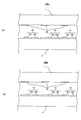
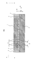
- FIG. 1 It is a figure which shows an example of the exploded perspective view of a displacement sensor. It is a figure which shows an example of sectional drawing of a displacement sensor. It is a figure which shows the structure of the capacitor
- FIG. 10 is an exploded perspective view of a displacement sensor in Example 4 and a diagram illustrating an example of a capacitor structure. 10 is a diagram illustrating an example of a capacitor structure in Example 5. FIG. It is a figure which shows an example of sectional drawing of the displacement sensor in Example 6.
- One aspect of the present invention is a displacement sensor that measures displacement based on a change in capacitance, and includes a plurality of teeth that are formed on the same surface and that are formed at a predetermined period with respect to a detection direction.
- a detection electrode and a movable structure having a facing surface parallel to the detection electrode and displaced in an in-plane direction of the facing surface, and the movable structure is arranged at the predetermined period on the facing surface.
- a first region, and a second region adjacent to the first region and formed around the first region, and the first region in the tooth extending direction. Both ends of the portion that substantially contributes to the detection of capacitance are inside the both ends of the tooth.
- the above displacement sensor has a detection electrode and a movable structure, and detects the displacement of the movable structure.
- the detection electrode has a plurality of teeth formed according to a predetermined cycle on the same surface.
- the movable structure has a facing surface parallel to the detection electrode at a predetermined interval, and is displaced in the in-plane direction.
- the movable structure has a first region arranged at the same period as a tooth cycle on the opposite side, and a second region adjacent to the first region and formed around the first region. Have.
- the detection electrode forms a capacitor with the first and second regions. In the tooth extending direction, both ends of the portion that substantially contributes to the capacitance detection of the first region exist inside the both ends of the tooth.
- both ends of the first region described above are both ends of the teeth.
- the area of the capacitor that the detection electrode forms with the first region and the area of the capacitor that the detection electrode forms with the second region are not changed by the amount existing inside the capacitor. That is, in this case, the detected capacitance does not change. Therefore, the displacement sensor can appropriately measure the displacement in the detection direction even when the movable structure is displaced in the in-plane direction in a direction different from the detection direction. Further, the displacement sensor can appropriately measure the displacement in each detection direction even when detecting the displacement in two directions perpendicular to the in-plane direction at the same time.
- both ends of a portion that substantially contributes to detection of the capacitance of the first region in the extending direction are at least movable in the direction with respect to both ends of the teeth.
- both ends of a portion that substantially contributes to detection of the capacitance of the first region in the extending direction are in the extending direction with respect to both ends of the teeth. Is located on the inner side of the sum of the maximum displacement of the movable structure and the manufacturing error in the extending direction. By doing so, the displacement sensor can appropriately measure the displacement in the detection direction even if a manufacturing error occurs.
- the facing surface has a concavo-convex structure
- the first region is a convex portion of the concavo-convex structure
- the second region is a concave portion of the concavo-convex structure.
- the convex portion and the concave portion are the same member.
- the capacitance of a capacitor is inversely proportional to the capacitor distance. Therefore, according to this aspect, the displacement sensor has a capacitance per unit area of the capacitor formed by the first region and the first electrode, and a unit of the capacitor formed by the second region and the first electrode. A difference can be provided between the capacitance per area. That is, the displacement sensor can perform differential detection based on a change in capacitance.
- the first region is defined by an electrode foil formed on the movable structure.
- This electrode foil is formed, for example, by a method such as vapor deposition of metal particles through a mask, sputtering, or etching.
- the electrode foil is periodically bonded to the opposing surfaces of the movable structure and the second electrode.
- the displacement sensor can perform differential detection by making the movable structure an insulator.
- the rate of change in capacitance with respect to the amount of displacement can be increased. That is, the displacement sensor can perform highly sensitive displacement detection.
- the displacement sensor further includes a detection unit that is electrically connected to the detection electrode and detects a displacement amount of the movable structure based on a capacitance detected from the detection electrode. By doing so, the displacement sensor can detect the displacement based on the detected capacitance by the detection unit.
- FIG. 1 shows an example of an exploded perspective view of a displacement sensor 100 in the present embodiment.
- FIG. 2 shows an example of a cross-sectional view taken along a cutting plane AA ′ of the displacement sensor 100.
- the displacement sensor 100 includes a movable structure 1, a support substrate 2, a frame portion 3, a support spring 4, and a detection electrode 10.
- the displacement sensor 100 is a sensor that detects the displacement of the movable structure 1 in the x-axis direction and the y-axis direction.
- the displacement sensor 100 detects displacement based on the capacitance detected from the detection electrode 10 as will be described later.
- the movable structure 1 is a member that can be displaced in the x-axis direction and the y-axis direction shown in FIG.
- the movable structure 1 is connected to the support spring 4 and is displaced within the space partitioned by the frame portion 3.
- the movable structure 1, the frame portion 3, and the support spring 4 are made of, for example, a silicon substrate, and more specifically, are formed by performing MEMS (Micro Electro Mechanical Systems) processing on the silicon substrate.
- MEMS Micro Electro Mechanical Systems
- An uneven portion 11 is formed on the lower surface of the movable structure 1, that is, on the surface (facing the surface) facing the detection electrode 10.
- the concavo-convex portion 11 includes a convex portion 11a and a concave portion 11b.
- the concavo-convex portion 11 is arranged to face the detection electrode 10 in parallel, that is, to face each other.
- grooved part 11 and the detection electrode 10 form a capacitor
- the concavo-convex portion 11 is made of the same member as the movable structure 1.
- the frame 3 is connected to the support spring 4 and is formed so as to surround the movable structure 1. As shown in FIG. 2, the frame portion 3 is joined to the support substrate 2 so that the concavo-convex portion 11 and the detection electrode 10 face each other. Specifically, the frame portion 3 and the support substrate 2 are bonded using a bonding technique such as anodic bonding, fusion bonding, direct bonding, or plasma activated bonding.
- a bonding technique such as anodic bonding, fusion bonding, direct bonding, or plasma activated bonding.
- the support substrate 2 is made of glass, for example, and has a rectangular recess (indentation) 7 on an upper surface portion facing the movable structure 1.
- the recess 7 of the support substrate 2 has a larger area than the lower surface of the movable structure 1 as shown in FIG.
- the detection electrode 10 is disposed in the recess 7.
- the detection electrode 10 includes a first electrode 10a and a second electrode 10b.
- the first electrode 10a has a comb-tooth structure.
- the surface of the first electrode 10a has a comb shape with a plurality of teeth located in parallel with the xy plane and extending in the negative direction of the y axis in FIG.
- the second electrode 10b has a comb-tooth structure.
- the surface of the second electrode 10b has a plurality of teeth that are located in parallel with the xy plane in FIG. 1 and extend in the positive direction of the y-axis.
- teeth extension direction the direction in which the teeth of the first electrode 10a extend (here, the negative direction of the y-axis) and the direction in which the teeth of the second electrode 10b extend (here, the positive direction of the y-axis). This is simply called “tooth extension direction”.
- the teeth of the first electrode 10a and the teeth of the second electrode 10b are alternately arranged on the same plane (xy plane) at a predetermined interval. . Further, the direction in which the teeth of the first electrode 10a and the teeth of the second electrode 10b are aligned corresponds to the direction in which the displacement is detected (hereinafter simply referred to as “detection direction”).
- the detection electrode 10 is made of, for example, platinum and chromium, aluminum, or platinum and titanium.
- the first electrode 10a is the same member as the second electrode 10b.
- FIG. 3 is an example of an enlarged view of a part of the capacitor formed by the detection electrode 10 and the concavo-convex portion 11 shown in the range of the broken line frame 70 in FIG.
- the plurality of teeth 10ax of the first electrode 10a are formed with a predetermined period P.
- the plurality of teeth 10bx of the second electrode 10b are formed with the same period P.
- the teeth 10ax of the first electrode 10a and the teeth 10bx of the second electrode 10b are alternately arranged in the x direction on the same plane.
- the concavo-convex portion 11 is formed with a period P as shown in FIG.
- the convex portion 11a faces the tooth 10ax in a state where there is no displacement. That is, the convex portion 11a has the largest overlap (opposite area) in the xy plane with the teeth 10ax of the first electrode 10a.
- the recessed part 11b opposes the tooth
- the recessed part 11b is arrange
- the capacitor formed by the detection electrode 10 and the concavo-convex portion 11 has a predetermined capacitance.
- first capacitance C1 the capacitance of the capacitor formed by the first electrode 10a and the concavo-convex portion 11
- second capacitance C2 the capacitance of the capacitor formed by the second electrode 10b and the concavo-convex portion 11
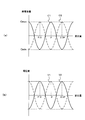
- FIG. 4A shows an example of a graph of changes in the first capacitance C1 and the second capacitance C2 due to the displacement of the movable structure 1.
- a horizontal axis shows the displacement amount of the movable structure 1
- shaft shows an electrostatic capacitance.
- the “displacement amount” indicates a value (distance) by which the movable structure 1 is displaced in the x direction or the y direction.
- the relationship between the first capacitance C1 and the second capacitance C2 detected by the detection electrode 10 disposed in the broken line frame 70 and the displacement in the detection direction (x-axis direction) will be described. To do.
- the distance between the detection electrode 10 and the convex portion 11a is smaller than the distance between the detection electrode 10 and the concave portion 11b.
- the electrostatic capacity is inversely proportional to the distance between the pair of electrodes constituting the capacitor, and the convex portion 11a is the same member as the concave portion 11b. Accordingly, the capacitance per unit area of the capacitor formed by the convex portion 11 a and the detection electrode 10 is larger than the capacitance per unit area of the capacitor formed by the concave portion 11 b and the detection electrode 10.
- the 1st electrode 10a opposes the convex part 11a, and forms the convex part 11a and a capacitor
- the first capacitance C1 takes the maximum value “Cmax” as shown in FIG. 4A in a state where there is no displacement.
- the second electrode 10b is opposed to the recess 11b and forms a capacitor with the recess 11b. Therefore, the second capacitance C2 takes the minimum value “Cmin” in a state where there is no displacement. Note that the phases of the capacitances C1 and C2 in a state where there is no displacement are not limited to those in FIG. 4 and may be set to any state.
- the area of the capacitor formed by the first electrode 10a and the recess 11b increases, and the first The area of the capacitor formed by the electrode 10a and the protrusion 11a (that is, the area where the first electrode 10a and the plurality of protrusions 11a face each other) decreases. Accordingly, the first capacitance C1 decreases until the displacement amount reaches P / 2, that is, until the area where the teeth 10ax of the first electrode 10a face the recess 11b is maximized.
- the first capacitance C1 takes the minimum value Cmin when the displacement is P / 2. Then, as shown in FIG.
- the first capacitance C1 alternately takes a maximum value Cmax and a minimum value Cmin every time the displacement amount increases by P / 2.
- the second capacitance C2 alternately takes the maximum value Cmax and the minimum value Cmin every time the displacement amount increases by P / 2. Therefore, the first electrostatic capacity C1 and the second electrostatic capacity C2 are 180 degrees out of phase as shown in FIG. Note that the phase between the capacitances C1 and C2 and the phase of the output voltage value in a state where there is no displacement may be set arbitrarily. For example, in addition to the case where the phase difference is 180 ° as described above, an arbitrary phase difference can be provided in consideration of the offset. In this case, it is necessary to consider that a phase offset is necessary and that the output voltage value is reduced. However, the phase may be set within a possible range where an output voltage value necessary for detection can be obtained.
- both ends of the tooth indicate a terminal portion in the extending direction of the tooth and an end portion of the root portion (dashed line portion) of the tooth.
- the convex portion 11a is surrounded by a concave portion 11b (not shown). Then, both end portions (end surfaces) 11aa and 11ab of the convex portion 11a in the tooth extending direction (y-axis direction) are inside the end portion 10axa and the end portion 10axb of the tooth 10ax in the tooth extending direction, that is, between It exists in the position sandwiched between. In other words, even if the convex portion 11a has a predetermined displacement in the in-plane direction and in the direction perpendicular to the detection direction (y-axis direction), the area of the first electrode 10a facing the tooth 10ax does not vary. Are formed and arranged.
- the end portion 11aa and the end portion 11ab of the convex portion 11a in the tooth extending direction exist inside the both end portions of the tooth 10bx in the tooth extending direction.
- the displacement sensor 100 can robustly detect the displacement in the detection direction even when the displacement is different from the detection direction.
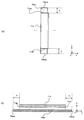
- FIG. 5 is an enlarged view of a pair of teeth 10ax and convex portions 11a of the first electrode 10a facing each other in FIG.
- FIG. 5A shows an enlarged view of the teeth 10ax and the protrusions 11a of the first electrode 10a in the xy plane
- FIG. 5B shows the teeth of the first electrode 10a in the yz plane.
- the enlarged view of 10ax and the convex part 11a is shown.
- the length of the tooth 10ax in the tooth extending direction is longer than the length of the convex portion 11a in the tooth extending direction.
- the end portions 11aa and 11ab of the convex portion 11a exist inside the tooth 10ax by a predetermined distance “d” with respect to the end portion 10axa and the end portion 10axb of the tooth 10ax, respectively.
- the displacement sensor 100 can accurately detect the displacement in the detection direction by appropriately providing the distance d.
- the distance “d” is, for example, an error (such as a maximum displacement in the tooth extending direction, a displacement (alignment displacement) between the detection electrode 10 and the concavo-convex portion 11 at the time of manufacturing the displacement sensor 100, a processing variation, and the like ( Hereinafter, it is simply set to be larger than the sum of “production error”.
- the above manufacturing error is measured or estimated in advance by an experiment or the like, for example. Accordingly, in FIGS. 5A and 5B, the distance d is set to be larger than the sum of the maximum displacement of the movable structure 1 in the y-axis direction and the manufacturing error estimated in advance.
- the displacement sensor 100 can appropriately detect the displacement in the x-axis direction regardless of the presence or absence of the displacement in the y-axis direction, and regardless of the presence or absence of the displacement in the x-axis direction.
- the displacement detection in the y-axis direction can be appropriately performed. That is, the displacement sensor 100 can independently detect displacements in the x-axis direction and the y-axis direction.
- the distance d between the end portion 10axa and the end portion 11aa in the tooth extending direction and the distance d between the end portion 10axb and the end portion 11ab may be different values. Even in this case, the distance d is preferably set larger than the sum of the maximum displacement in the tooth extending direction and the manufacturing error.
- FIG. 6 shows an example of a system for calculating the displacement amount.
- a detector 15 is arranged in the system.
- the detector 15 is electrically connected to the first electrode 10a and electrically connected to the second electrode 10b.
- the detection unit 15 detects the first capacitance C1 from the first electrode 10a, and detects the second capacitance C2 from the second electrode 10b.
- the detection unit 15 calculates the displacement amount of the movable structure 1 based on the detected first capacitance C1 and second capacitance C2. That is, the detection unit 15 differentially detects the displacement amount of the movable structure 1 based on the first capacitance C1 and the second capacitance C2.
- FIG. 4B shows a graph in which the first capacitance C1 and the second capacitance C2 shown in FIG. 4A are converted into voltage values (CV conversion).
- the voltage value calculated from the first capacitance C1 is expressed as a voltage value “V1”
- the voltage value calculated from the second capacitance C2 is expressed as a voltage value “V2”.
- the voltage value is inversely proportional to the capacitance. Accordingly, as shown in FIG. 4B, when the first capacitance C1 is larger than the second capacitance C2, the voltage value V1 becomes smaller than the voltage value V2. Similarly, when the second capacitance C1 is smaller than the second capacitance C2, the voltage value V1 is larger than the voltage value V2.
- FIG. 7A shows a voltage value obtained by differential amplification after the detection unit 15 converts the first capacitance C1 and the second capacitance C2 into voltage values (hereinafter simply referred to as “output”). An example of a graph of “voltage value” is shown.
- the first capacitance C1 takes the maximum value Cmax, and the second capacitance C2 takes the minimum value Cmin. That is, in this case, the voltage value V1 takes the minimum value, and the voltage value V2 takes the maximum value. Therefore, the output voltage value takes the minimum value “Vmin” in a state where there is no displacement.
- the first capacitance C1 decreases and the second capacitance C2 increases until the amount of displacement reaches P / 2 from the state where there is no displacement. That is, the voltage value V1 increases and the voltage value V2 decreases. Therefore, in this case, the output voltage value increases.
- the displacement amount is P / 2
- the output voltage value takes the maximum value “Vmax”.
- the output voltage value decreases again, and takes the minimum value Vmin when the displacement amount is P.
- the output voltage value has a maximum value Vmax and a minimum value every time the displacement amount changes by P / 2.
- the value Vmin is alternately taken. That is, the output voltage value periodically changes as the displacement amount changes.
- the output voltage value changes periodically every time the displacement amount changes by the period P.
- the detection unit 15 stores a map of the output voltage value and the displacement as shown in FIG. 7A in the memory in advance, and estimates the displacement amount by comparing with the detected output voltage value. Can do.
- the detection unit 15 performs differential detection based on the first capacitance C1 and the second capacitance C2, it removes common-mode noise caused by temperature fluctuations, vibrations, changes in airflow, and the like. be able to. That is, the detection unit 15 can measure the displacement by performing differential detection without being affected by the common-mode noise.
- the phases of the capacitances C1 and C2 and the phase of the output voltage value in a state where there is no displacement may be arbitrarily set.
- the period P is set to be equal to or less than the maximum displacement amount (hereinafter simply referred to as “maximum displacement”) in the x-axis direction (detection direction) in which the comb teeth are arranged.
- the maximum displacement is measured or estimated based on, for example, a space partitioned by the frame portion 3.
- the detection unit 15 can, for example, determine the number of times the minimum value Vmin is reached again, that is, the number of fluctuation periods of the output voltage value and the final output voltage value. Based on this, it is possible to detect a displacement of the period P or more.
- the detection unit 15 can also measure a large displacement of the movable structure 1 by counting the number of fluctuation periods of the output voltage value.
- the displacement sensor 100 can be used as a linear encoder, for example.
- the detection unit 15 can measure the large displacement of the movable structure 1 with high resolution by making the period P smaller than the maximum displacement.
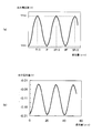
- FIG. 7B shows a graph of the actual measurement value of the output voltage value with respect to the displacement amount of the movable structure 1.
- FIG. 7B shows the measurement by moving the movable structure 1 every 20 nm, and the period P of the teeth 10ax of the first electrode 10a and the teeth 10bx of the second electrode 10b at this time is 20 ⁇ m.
- the displacement sensor according to the present invention includes the detection electrode and the movable structure, and detects the displacement of the movable structure.
- the detection electrode has a shape having a plurality of teeth formed according to a predetermined cycle on the same surface.
- the movable structure has a facing surface parallel to the detection electrode at a predetermined interval, and is displaced in the in-plane direction.
- a movable structure has a convex part arrange
- the detection electrode forms an uneven portion and a capacitor.
- both ends of the convex portion exist inside the both ends of the tooth.
- detection is performed because the both ends of the above-described convex portion exist inside the both ends of the tooth.
- the area of the capacitor formed by the electrode and the concave portion and the area of the capacitor formed by the detection electrode and the concave portion do not change, and the detected capacitance does not change. Accordingly, the displacement sensor can appropriately measure the displacement in the detection direction even when the movable structure is displaced in a direction different from the detection direction.
- the displacement sensor can appropriately measure the displacement in each detection direction even when detecting the displacement in two perpendicular directions in the in-plane direction at the same time.
- Example 2 In Example 1, the convex part 11a had a rectangular parallelepiped shape. However, the shape of the convex portion 11a to which the present invention is applicable is not limited to this.
- FIG. 8A shows a positional relationship on the xy plane between the projection 11a and the first electrode 10a when the end of the projection 11a is deformed.
- the end portion 11aa has a stepped shape.
- the end portion 11ab has a triangular shape.
- FIG. 8B shows a positional relationship on the yz plane between the convex portion 11a and the first electrode 10a according to the second embodiment.
- the end 11aa and the end 11ab of the convex portion 11a according to the second embodiment are connected to the end 10axa of the first electrode 10a and the end in the tooth extending direction (y-axis direction) It exists outside the part 10axb.
- the area in the vicinity of the end portion 11aa and the vicinity of the end portion 11ab is small. Specifically, the vicinity of the end portion 11aa and the vicinity of the end portion 11ab hardly contribute to the capacitance of the capacitor formed by the convex portion 11a and the first electrode 10a. Therefore, in this case, both ends in the tooth extending direction of the convex portion 11a are determined based only on the portion of the convex portion 11a that substantially contributes to the detection of capacitance.
- “substantially contribute” means, for example, a portion that hardly contributes to the capacitance of the capacitor such as the vicinity of the end 11aa and the vicinity of the end 11ab in the electrode structure as described above. It is described with the purpose of excluding it.
- the vicinity of the end portion 11aa and the vicinity of the end portion 11ab may contribute to the capacitance of the capacitor in a negative aspect such as disturbance or parasitic capacitance.
- a negative contribution does not fall within the “substantially contribution” defined in this embodiment.
- the width in the detection direction (x-axis direction) of the portion where the convex portion 11a faces the first electrode 10a is defined as a width “h” as shown in FIG.
- the “portion that substantially contributes to the detection of capacitance” is, for example, the width in the x-axis direction (when including an intermittent portion, the width of the intermittent portion is excluded) h. / 2 or more.
- the portion outside the broken line 11aay and the portion outside the broken line 11aby correspond to the “parts that substantially contribute to the detection of capacitance”. do not do.
- the end portion in the tooth extending direction of the portion that substantially contributes to the capacitance detection of the convex portion 11a is determined to be at the position indicated by the broken lines 11aaay and 11aby. Further, the broken lines 11aaay and 11aby exist inside the tooth 11ax by a distance d with respect to the end 10axa and the end 10axb in the tooth extending direction. Therefore, even if the movable structure 1 is displaced within the distance d in the tooth extending direction which is perpendicular to the detection direction, the value of the detected first capacitance C1 hardly fluctuates.
- the displacement sensor 100 can perform xy independent detection appropriately by setting the distance d appropriately like Example 1.
- the displacement sensor 100 includes a detection electrode 10 for detecting displacement in the x-axis direction and a detection electrode 10 for detecting displacement in the y-axis direction, and a plurality of detections in each direction.
- the electrode 10 was included.
- the displacement sensor according to the present invention may detect only one direction and have only one detection electrode 10 instead.
- FIG. 9 shows an example of an exploded perspective view of the displacement sensor 100a in which one detection electrode 10 is arranged.
- the displacement sensor 100a detects a displacement in the x-axis direction.
- the movable structure 1 may be displaced in the y-axis direction that is perpendicular to the detection direction in the in-plane direction.
- both end portions of the convex portion 11a are arranged on the inner side of the tooth 11ax by the distance d, and the convex portion 11a Both ends are arranged inside the tooth 11bx by a distance d.
- the displacement sensor 100a can appropriately detect the displacement in the detection direction without being affected by the displacement in the direction perpendicular to the detection direction.
- Example 4 In Example 1, the detection electrode 10 was formed of the first electrode 10a and the second electrode 10b. Then, the displacement sensor 100 detects the displacement of the movable structure 1 based on the first capacitance C1 detected from the first electrode 10a and the second capacitance C2 detected from the second electrode 10b. It was differentially detected. On the other hand, in the displacement sensor according to the present invention, instead of this, the detection electrode 10 may be constituted by one electrode.
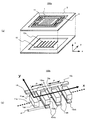
- FIG. 10A shows an example of an exploded perspective view of the displacement sensor 100b according to the fourth embodiment.
- the detection electrode 10 consists of one electrode, and has the tooth
- FIG. 10B is an example of a diagram showing a positional relationship between the detection electrode 10 and the convex portion 11a.
- the detection electrode 10 faces the convex portion 11a.
- the end surfaces 11aa and 11ab of the convex portion 11a are located inside the distance d with respect to the end portion 10xa and the end portion 10xb of the tooth 10x.
- the displacement sensor 100b can measure the displacement in the detection direction independently of the displacement in the tooth extending direction.
- the displacement sensor 100 b detects the capacitance from the detection electrode 10.
- the detection unit 15 holds, for example, a map of the relationship between the capacitance and the amount of displacement as shown in FIG.
- the detection part 15 which concerns on Example 4 can measure a displacement amount based on the electrostatic capacitance detected from the detection electrode 10 with reference to the said map.
- the edge part of the convex part 11a has deform
- the movable structure 1 has the concavo-convex portion 11 on the lower surface, and the concavo-convex portion 11 and the detection electrode 10 form a capacitor.
- the configuration of the displacement sensor 100 to which the present invention can be applied is not limited to this, and the movable structure 1 does not necessarily have the uneven portion 11.
- FIG. 11 shows an example of an enlarged view of the capacitor portion of the displacement sensor in the fifth embodiment.
- the movable structure 1 does not have an uneven portion on the lower surface portion.
- the movable structure 1 is formed with an electrode foil 20 such as a metal thin film forming an electrode on the lower surface thereof according to a predetermined cycle.
- This electrode foil is formed, for example, by a method such as vapor deposition of metal particles through a mask, sputtering, or etching.
- the electrode foil 20 is disposed so as to face the first electrode 10a in a state where there is no displacement. That is, the electrode foil 20 is formed every period P.
- the movable structure 1 is an insulator such as lead zirconate titanate.
- the first electrode 10a and the second electrode 10b form a capacitor with the electrode foil 20 and have a capacitance.
- the first electrode 10 a and the second electrode 10 b do not have a capacitance with the movable structure 1. Accordingly, as shown in FIG. 11A, in the state where there is no displacement, the first electrode 10a is opposed to the electrode foil 20, so that a capacitor is formed and a predetermined capacitance is generated.
- the second electrode 10b does not oppose the electrode foil 20, but opposes the movable structure 1 made of an insulator member, so that the capacitance is zero.
- the displacement sensor 100c can perform differential detection based on the first capacitance C1 and the second capacitance C2. Further, by appropriately selecting the member of the electrode foil 20, the displacement sensor 100c can increase the maximum value Cmax of the capacitance, and the difference between the maximum value Cmax and the minimum value Cmin (here, 0) is obtained. Can be bigger. Therefore, the displacement sensor 100c can detect the displacement with higher sensitivity.
- the displacement sensor 100d in FIG. 11B a concave space for fitting the electrode foil 20 is formed on the lower surface of the movable structure 1 according to a predetermined period. Therefore, the lower surface of the movable structure 1 and the lower surface portion of the electrode foil 20 are configured on the same surface, and the movable structure 1 and the electrode foil 20 do not have an uneven structure as a whole. Even if comprised in this way, the displacement sensor 100d can detect differentially based on the 1st electrostatic capacitance C1 and the 2nd electrostatic capacitance C2 similarly to the displacement sensor 100d.
- the support substrate 2 has a recess 7 having a larger area than the lower surface of the movable structure 1.
- the configuration of the displacement sensor 100 to which the present invention is applicable is not limited to this.
- FIG. 12 is a cross-sectional view of the displacement sensor 100 according to the second embodiment.
- the upper surface of the support substrate 2 (the surface on the side facing the movable structure 1) is flat, and does not have the concave portion 7 as in the first embodiment.
- the support substrate 2 is connected to the frame portion 3 at the edge of the upper surface.
- a detection electrode 10 is disposed on the upper surface portion of the support substrate 2.
- the movable structure 1 and the support spring 4 are arranged with a predetermined distance from the support substrate 2 and the detection electrode 10. That is, the lower surface of the movable structure 1 and the support spring 4, that is, the surface facing the support substrate 2 is recessed from the lower surface of the frame portion 3. Even in such a configuration, the displacement sensor 100e can appropriately detect the displacement of the movable structure 1.
- the present invention can be used for a displacement sensor for detecting a displacement amount. Further, it can be widely applied to acceleration sensors, pressure sensors, force sensors and the like.
Landscapes
- Engineering & Computer Science (AREA)
- Physics & Mathematics (AREA)
- General Physics & Mathematics (AREA)
- Power Engineering (AREA)
- Chemical & Material Sciences (AREA)
- Analytical Chemistry (AREA)
- Computer Hardware Design (AREA)
- Microelectronics & Electronic Packaging (AREA)
- Pressure Sensors (AREA)
Abstract
変位センサは、検出電極と、可動構造とを有し、可動構造の変位を検出する。検出電極は、同一面上に所定の周期に従って形成された複数の歯を有する。可動構造は、検出電極と所定間隔をもって平行する対面を有し、面内方向において変位する。可動構造は、対面において、歯の周期と同一周期ごとに配置される第1の領域と、第1の領域と隣接し、かつ第1の領域の周囲に形成される第2の領域と、を有する。検出電極は、第1及び第2の領域とコンデンサを形成する。そして、歯延在方向において、第1の領域の静電容量検出に実質的に寄与する部分の両端は、歯の両端の内側に存在する。
Description
本発明は、静電容量の変化に基づき可動部分の変位を測定する変位センサに関する。
静電容量の検出値に基づき可動構造(可動電極)の変位を検出する静電容量型変位センサが既知である。例えば、非特許文献1には、可動構造下部に線状電極が周期的に並ぶ櫛歯電極が形成された静電容量型変位センサが記載されている。また、特許文献1には、可動構造に凹凸の溝を構成することでコンデンサを実現する技術が記載されている。
一方、可動構造は、変位を検出する方向(検出方向)にのみ変位するとは限らない。この場合、変位センサは、検出方向と異なる方向に可動構造が変位した場合であっても、当該変位のうち検出方向の成分の変位を的確に検出する必要がある。従って、変位センサは、検出方向と垂直方向の変位に対するロバスト性が要求される。また、垂直関係にある2方向の変位を検出する場合、変位センサは、検出方向ごとの変位を独立して計測する必要がある。特許文献1及び非特許文献1には、これらの問題は何ら記載されていない。
本発明が解決しようとする課題としては、上記のようなものが例として挙げられる。本発明は、静電容量型の変位センサにおいて、可動構造が面内方向のうち検出方向とは異なる方向へ変位した場合であっても、適切に検出方向の変位を計測することを目的とする。
請求項1に記載の発明では、静電容量の変化に基づき変位を測定する変位センサであって、同一面上に形成され、かつ、検出方向に対し所定の周期で形成された複数の歯を有する検出電極と、前記検出電極と平行に対向する対面を有し、当該対面の面内方向に変位する可動構造と、を備え、前記可動構造は、前記対面において、前記所定の周期で配置される第1の領域と、前記第1の領域と隣接し、前記第1の領域の周囲に形成される第2の領域と、を有し、前記歯の延在方向における、前記第1の領域の静電容量の検出に実質的に寄与する部分の両端は、前記歯の両端の内側に存在することを特徴とする。
1 可動構造
2 支持基板
3 枠部
4 支持ばね
10 検出電極
11 凹凸部
15 検出部
20 電極箔
100、100a~100e 変位センサ
2 支持基板
3 枠部
4 支持ばね
10 検出電極
11 凹凸部
15 検出部
20 電極箔
100、100a~100e 変位センサ
本発明の1つの観点では、静電容量の変化に基づき変位を測定する変位センサであって、同一面上に形成され、かつ、検出方向に対し所定の周期で形成された複数の歯を有する検出電極と、前記検出電極と平行に対向する対面を有し、当該対面の面内方向に変位する可動構造と、を備え、前記可動構造は、前記対面において、前記所定の周期で配置される第1の領域と、前記第1の領域と隣接し、前記第1の領域の周囲に形成される第2の領域と、を有し、前記歯の延在方向における、前記第1の領域の静電容量の検出に実質的に寄与する部分の両端は、前記歯の両端の内側に存在する。
上記の変位センサは、検出電極と、可動構造とを有し、可動構造の変位を検出する。検出電極は、同一面上に所定の周期に従って形成された複数の歯を有する。可動構造は、検出電極と所定間隔をもって平行する対面を有し、面内方向において変位する。可動構造は、対面において、歯の周期と同一周期ごとに配置される第1の領域と、第1の領域と隣接し、かつ第1の領域の周囲に形成される第2の領域と、を有する。検出電極は、第1及び第2の領域とコンデンサを形成する。そして、歯の延在方向において、第1の領域の静電容量検出に実質的に寄与する部分の両端は、歯の両端の内側に存在する。このようにすることで、面内方向であって変位の検出方向と垂直方向、即ち検出方向の横方向に変位が生じた場合であっても、上述した第1の領域の両端が歯の両端の内側に存在する分、検出電極が第1の領域と形成するコンデンサの面積、及び検出電極が第2の領域と形成するコンデンサの面積は変化しない。即ち、この場合、検出される静電容量は変化しない。従って、変位センサは、可動構造が面内方向に検出方向とは異なる方向へ変位した場合であっても、適切に検出方向における変位を計測することができる。また、変位センサは、面内方向の垂直関係にある2方向の変位を同時に検出する場合も、各検出方向における変位をそれぞれ適切に計測することができる。
上記の変位センサの一態様では、前記延在方向において、前記第1の領域の静電容量の検出に実質的に寄与する部分の両端は、前記歯の両端に対し、少なくとも前記方向における前記可動構造の最大変位より内側にそれぞれ存在する。このようにすることで、検出方向と垂直方向である歯延在方向に最大限の変位が発生した場合であっても、変位センサは、検出方向における変位の計測に影響を受けない。従って、変位センサは、適切に変位を検出することができる。
上記の変位センサの他の一態様では、前記延在方向において、前記第1の領域の静電容量の検出に実質的に寄与する部分の両端は、前記歯の両端に対し、前記延在方向における前記可動構造の最大変位と、前記延在方向の製作誤差との和より内側に存在する。このようにすることで、変位センサは、製作誤差が生じた場合であっても、検出方向における変位を適切に計測することができる。
上記の変位センサの一態様では、前記対面は凹凸構造を有し、前記第1の領域は前記凹凸構造の凸部であり、前記第2の領域は前記凹凸構造の凹部である。
上記の変位センサの好適な例では、前記凸部と前記凹部は同一部材である。コンデンサの静電容量はコンデンサの距離に反比例する。従って、変位センサは、この態様により、第1の領域と第1の電極とが形成するコンデンサの単位面積あたりの静電容量と、第2の領域と第1の電極とが形成するコンデンサの単位面積あたりの静電容量とに差を設けることができる。即ち、変位センサは、静電容量の変化に基づき差動検出をすることができる。
上記の変位センサの他の一態様では、前記第1の領域は、前記可動構造に形成された電極箔により区画されてなる。この電極箔は、例えばマスクを介した金属粒子の蒸着、スパッタ法、あるいはエッチングなどの方法により形成される。この態様では、可動構造の第1及び第2の電極と対向面に周期的に電極箔が接着されている。これにより、例えば可動構造を絶縁体にすることで、変位センサは、差動検出を実行することができる。さらに、形成させる電極箔を適切に選択することで、変位量に対する静電容量の変化の割合を大きくすることができる。即ち、変位センサは、感度の高い変位検出を行うことが可能となる。
上記の変位センサの他の一態様では、前記検出電極と電気的に接続し、前記検出電極から検出される静電容量に基づき前記可動構造の変位量を検出する検出部をさらに備える。このようにすることで、変位センサは、検出部により、検出された静電容量に基づき変位を検出することができる。
以下、図面を参照して本発明の好適な実施例について説明する。
[実施例1]
(概略構成)
図1は、本実施例における変位センサ100の分解斜視図の一例を示す。また、図2は、変位センサ100の切断面A-A´における断面図の一例を示す。図1及び図2に示すように、変位センサ100は、可動構造1と、支持基板2と、枠部3と、支持ばね4と、検出電極10と、を有する。
(概略構成)
図1は、本実施例における変位センサ100の分解斜視図の一例を示す。また、図2は、変位センサ100の切断面A-A´における断面図の一例を示す。図1及び図2に示すように、変位センサ100は、可動構造1と、支持基板2と、枠部3と、支持ばね4と、検出電極10と、を有する。
変位センサ100は、可動構造1のx軸方向及びy軸方向における変位を検出するセンサである。変位センサ100は、後述するように、検出電極10から検出される静電容量に基づき、変位検出を行う。
可動構造1は、図1に示すx軸方向及びy軸方向、即ち面内方向に変位可能な部材である。可動構造1は、支持ばね4と接続し、枠部3が仕切る空間の範囲内で変位する。可動構造1、枠部3、及び支持ばね4は、例えばシリコン基板により構成され、より具体的にはシリコン基板にMEMS(Micro Electro Mechanical Systems)加工を施すことにより形成される。
可動構造1の下面、即ち、検出電極10と向かい合う面(対面)上には、凹凸部11が形成されている。凹凸部11は、凸部11aと凹部11bとからなる。凹凸部11は、検出電極10と平行して向かい合うように、即ち、対向するように配置される。これにより、凹凸部11と検出電極10とは、コンデンサを形成する。即ち、シリコン材料からなる凹凸部11は、コンデンサの電極として機能する。本実施例において、凹凸部11は、可動構造1と同一部材からなる。
枠部3は、支持ばね4と接続し、可動構造1を囲むように形成される。図2に示すように、枠部3は、凹凸部11と検出電極10とが対向するように、支持基板2と接合している。具体的には、枠部3と支持基板2は、陽極接合、溶融接合、直接接合、またはプラズマ活性化接合などの接合技術を用いて接合される。
支持基板2は、例えばガラスからなり、可動構造1と向かい合う上面部分に矩形の凹部(くぼみ)7を有する。この支持基板2の凹部7は、図2に示すように、可動構造1の下面よりも大きな面積を有する。そして、支持基板2は、凹部7に検出電極10が配置されている。
検出電極10は、第1の電極10aと、第2の電極10bと、からなる。第1の電極10aは櫛歯構造を有する。即ち、第1の電極10aの面は、図1において、xy面と平行に位置し、y軸の負の方向に延在する複数の歯を備えた櫛歯形状を有する。第2の電極10bは、第1の電極10aと同様に、櫛歯構造を有する。即ち、第2の電極10bの面は、図1において、xy面と平行に位置し、y軸の正の方向に延在する複数の歯を有する。以後、第1の電極10aの歯が延在する方向(ここでは、y軸の負の方向)及び第2の電極10bの歯が延在する方向(ここでは、y軸の正の方向)を、単に「歯延在方向」と呼ぶ。
図1及び図2に示すように、第1の電極10aの歯と、第2の電極10bの歯とは、同一面(xy面)上に所定の間隔を隔てて交互に並んで配置される。また、第1の電極10aの歯及び第2の電極10bの歯が並ぶ方向は、変位を検出する方向(以後、単に「検出方向」と呼ぶ。)と一致する。検出電極10は、例えば、白金及びクロム、またはアルミ、若しくは白金及びチタンによりなる。また、第1の電極10aは、第2の電極10bと同一部材である。
(コンデンサの構造)
図3は、図1の破線枠70の範囲内に示す検出電極10と凹凸部11とにより形成されるコンデンサの一部を拡大した図の一例である。なお、図3においては、図示の便宜上、凹凸部11の凸部11aのみを図示している。図3に示すように、第1の電極10aの複数の歯10axは、所定の周期Pを有して形成される。同様に、第2の電極10bの複数の歯10bxは、同じ周期Pを有して形成される。そして、上述のように、第1の電極10aの歯10axと、第2の電極10bの歯10bxは、同一面上においてx方向に交互に並んで配置されている。
図3は、図1の破線枠70の範囲内に示す検出電極10と凹凸部11とにより形成されるコンデンサの一部を拡大した図の一例である。なお、図3においては、図示の便宜上、凹凸部11の凸部11aのみを図示している。図3に示すように、第1の電極10aの複数の歯10axは、所定の周期Pを有して形成される。同様に、第2の電極10bの複数の歯10bxは、同じ周期Pを有して形成される。そして、上述のように、第1の電極10aの歯10axと、第2の電極10bの歯10bxは、同一面上においてx方向に交互に並んで配置されている。
凹凸部11は、図3に示すように、周期Pを有して形成される。本実施例において、凸部11aは、変位がない状態において、歯10axと対向する。即ち、凸部11aは、第1の電極10aの歯10axとxy平面における重なり(対向面積)が最大となっている。そして、凹部11bは、変位がない状態において、第2の電極10bの歯10bxと対向する。また、凹部11bは、凸部11aの周りを囲むように配置される。
検出電極10と凹凸部11とにより形成されるコンデンサは、所定の静電容量を有する。以後、第1の電極10aと凹凸部11とにより形成されるコンデンサの静電容量を「第1の静電容量C1」と表現する。同様に、第2の電極10bと凹凸部11とにより形成されるコンデンサの静電容量を「第2の静電容量C2」と表現する。
第1の静電容量C1及び第2の静電容量C2は、可動構造1が変位することにより値が変化する。これについて、図4(a)を用いて説明する。図4(a)は、可動構造1の変位に伴う第1の静電容量C1及び第2の静電容量C2の変化のグラフの一例を示す。図4(a)において、横軸は、可動構造1の変位量を示し、縦軸は、静電容量を示す。ここで、「変位量」は、x方向またはy方向に可動構造1が変位した値(距離)を示す。以後、一例として、破線枠70内に配置された検出電極10が検出する第1の静電容量C1及び第2の静電容量C2と、検出方向(x軸方向)における変位との関係について説明する。
ここで、検出電極10と凸部11aとの距離は、検出電極10と凹部11bとの距離よりも小さい。また、静電容量はコンデンサを構成する一対の電極の距離に反比例し、凸部11aは凹部11bと同一部材である。従って、凸部11aが検出電極10と形成するコンデンサの単位面積あたりの静電容量は、凹部11bが検出電極10と形成するコンデンサの単位面積あたりの静電容量よりも大きい。そして、変位がない状態において、第1の電極10aは、凸部11aと対向し、凸部11aとコンデンサを形成する。従って、第1の静電容量C1は、変位がない状態において、図4(a)に示すように、最大値「Cmax」をとる。一方、変位がない状態において、第2の電極10bは、凹部11bと対向し、凹部11bとコンデンサを形成する。従って、第2の静電容量C2は、変位がない状態において、最小値「Cmin」をとる。なお、変位がない状態における静電容量C1とC2との位相は図4に限られず任意の状態に設定してもよい。
そして、変位量が増加するに従い、第1の電極10aと凹部11bとが形成するコンデンサの面積(即ち、第1の電極10aと複数の凹部11bとが対向する面積)が増えるとともに、第1の電極10aと凸部11aとが形成するコンデンサの面積(即ち、第1の電極10aと複数の凸部11aとが対向する面積)が減少する。従って、第1の静電容量C1は、変位量がP/2に達するまで、即ち、第1の電極10aの歯10axが凹部11bと対向する面積が最大になるまで、減少する。そして、第1の静電容量C1は、変位量がP/2の場合に、最小値Cminをとる。そして、第1の静電容量C1は、図4(a)に示すように、変位量がP/2増加するごとに最大値Cmaxと最小値Cminとを交互にとる。同様に、第2の静電容量C2は、変位量がP/2増加するごとに最大値Cmaxと最小値Cminとを交互にとる。従って、第1の静電容量C1と第2の静電容量C2とは、図4(a)に示すように、位相が180度異なっている。なお変位がない状態における静電容量C1とC2との位相や出力電圧値の位相は任意に設定してもよい。例えば上記のように位相差が180°となる場合の他に、オフセットを考慮して任意の位相差を設けることもできる。この場合は位相のオフセットが必要であることと、出力電圧値は低減することを加味しなければならないが、検出に必要な出力電圧値が得られる可能な範囲で位相を設定してもよい。
(xy独立検出)
次に、可動構造1の面内方向における変位を、x軸方向の変位と、y軸方向の変位とにそれぞれ適切に分けて検出する方法(xy独立検出方法)について述べる。以後、「歯の両端部」は、歯の延在方向の終端部と、歯の付け根部分(破線部分)の端部とを示すものとする。
次に、可動構造1の面内方向における変位を、x軸方向の変位と、y軸方向の変位とにそれぞれ適切に分けて検出する方法(xy独立検出方法)について述べる。以後、「歯の両端部」は、歯の延在方向の終端部と、歯の付け根部分(破線部分)の端部とを示すものとする。
図3において、凸部11aは、図示しない凹部11bによって囲まれている。そして、歯延在方向(y軸方向)における凸部11aの両端部(端面)11aa及び11abは、歯延在方向において、歯10axの端部10axaと端部10axbとの内側に、即ち、間に挟まれる位置に存在する。言い換えると、凸部11aは、面内方向かつ検出方向と垂直方向(y軸方向)に所定の変位があった場合であっても、第1の電極10aの歯10axと対向する面積が変動しないように形成され、かつ配置されている。さらに、歯延在方向における凸部11aの端部11aa及び端部11abは、歯延在方向において、歯10bxの両端部の内側に存在する。以上のように、検出電極10及び凸部11aを構成することで、変位センサ100は、検出方向とは異なる変位に対しても頑強に検出方向における変位を検出することができる。
これについて図5を用いてさらに説明する。図5は、図3において対向する第1の電極10aの歯10ax及び凸部11aの1組を拡大した図である。具体的には、図5(a)は、xy平面における第1の電極10aの歯10ax及び凸部11aの拡大図を示し、図5(b)は、yz平面における第1の電極10aの歯10ax及び凸部11aの拡大図を示す。
図5(a)及び図5(b)に示すように、歯10axの歯延在方向(y軸方向)における長さは、凸部11aの歯延在方向における長さより長い。そして、歯延在方向において、凸部11aの端部11aa及び11abは、歯10axの端部10axaと端部10axbとに対し、所定距離「d」だけそれぞれ歯10axの内側に存在する。これにより、距離dの範囲内で検出方向と垂直方向である歯延在方向に凸部11aが変位した場合であっても、凸部11aと第1の電極10aとが形成するコンデンサの面積は変動しない。即ち、コンデンサを形成する凸部11aと第1の電極10aとが対向する面積に変動がない。従って、この場合、第1の静電容量C1及び第2の静電容量C2は変化しない。つまり、第1の静電容量C1及び第2の静電容量C2は、検出方向と垂直方向である歯延在方向の変位に影響を受けることなく、検出方向のみの変位に起因して値が変動する。従って、変位センサ100は、適切に距離dを設けることで、検出方向における変位を正確に検出することができる。
そして、距離「d」は、例えば、歯延在方向における最大変位と、変位センサ100の製作時における検出電極10と凹凸部11との配置ずれ(アライメントずれ)や加工ばらつき等に起因する誤差(以後、単に「製作誤差」と呼ぶ。)との和よりも大きく設定される。上述の製作誤差は、例えば、実験等により予め測定または推定される。従って、図5(a)及び図5(b)において、距離dは、y軸方向における可動構造1の最大変位と予め見積もった製作誤差との和よりも大きく設定される。このように距離dを設定することで、変位センサ100は、y軸方向の変位の有無によらず適切にx軸方向の変位検出を実行でき、かつ、x軸方向の変位の有無によらず適切にy軸方向の変位検出を実行することができる。即ち、変位センサ100は、x軸方向及びy軸方向の変位をそれぞれ独立して検出することができる。
なお、歯延在方向の端部10axaと端部11aaとの距離dと、端部10axbと端部11abとの距離dとは、それぞれ異なる値であってもよい。この場合であっても、距離dは、歯延在方向における最大変位と製作誤差との和よりも大きく設定されるのが好ましい。
(変位量の検出方法)
次に、検出した第1の静電容量C1と第2の静電容量C2とに基づき可動構造1の変位を検出する方法の一例を示す。図6は、変位量を算出するシステムの一例を示す。図6に示すように、当該システムには、検出部15が配置されている。検出部15は、第1の電極10aと電気的に接続するとともに、第2の電極10bと電気的に接続する。検出部15は、第1の電極10aから第1の静電容量C1を検出し、第2の電極10bから第2の静電容量C2を検出する。検出部15は、検出した第1の静電容量C1及び第2の静電容量C2に基づき、可動構造1の変位量を算出する。即ち、検出部15は、可動構造1の変位量を、第1の静電容量C1と第2の静電容量C2とに基づき差動検出する。
次に、検出した第1の静電容量C1と第2の静電容量C2とに基づき可動構造1の変位を検出する方法の一例を示す。図6は、変位量を算出するシステムの一例を示す。図6に示すように、当該システムには、検出部15が配置されている。検出部15は、第1の電極10aと電気的に接続するとともに、第2の電極10bと電気的に接続する。検出部15は、第1の電極10aから第1の静電容量C1を検出し、第2の電極10bから第2の静電容量C2を検出する。検出部15は、検出した第1の静電容量C1及び第2の静電容量C2に基づき、可動構造1の変位量を算出する。即ち、検出部15は、可動構造1の変位量を、第1の静電容量C1と第2の静電容量C2とに基づき差動検出する。
まず、検出部15は、第1の静電容量C1と、第2の静電容量C2とをそれぞれ電圧値に変換する。図4(b)は、図4(a)に示す第1の静電容量C1及び第2の静電容量C2を電圧値に変換(CV変換)したグラフを示す。以後、第1の静電容量C1から算出される電圧値を電圧値「V1」と表現し、第2の静電容量C2から算出される電圧値を電圧値「V2」と表現する。電圧値は静電容量に反比例する。従って、図4(b)に示すように、第1の静電容量C1が第2の静電容量C2よりも大きい場合、電圧値V1は電圧値V2よりも小さくなる。同様に、第2の静電容量C1が第2の静電容量C2よりも小さい場合、電圧値V1は電圧値V2よりも大きくなる。
次に、検出部15は、電圧値V1と電圧値V2とを差動増幅する。図7(a)は、検出部15が第1の静電容量C1と第2の静電容量C2とを電圧値に変換後、差動増幅して得られた電圧値(以後、単に「出力電圧値」と呼ぶ。)のグラフの一例を示す。
上述したように、変位がない状態において、第1の静電容量C1は最大値Cmaxをとり、第2の静電容量C2は最小値Cminをとる。即ち、この場合、電圧値V1は最小値をとり、電圧値V2は最大値をとる。よって、出力電圧値は、変位がない状態において、最小値「Vmin」をとる。そして、変位がない状態から変位量がP/2に達するまで、第1の静電容量C1は減少し、第2の静電容量C2は増加する。即ち、電圧値V1は増加し、電圧値V2は減少する。従って、この場合、出力電圧値は増加する。そして、変位量がP/2のとき、出力電圧値は最大値「Vmax」をとる。出力電圧値は、その後、再び減少し、変位量がPのとき、最小値Vminをとる。このように、出力電圧値は、第1の静電容量C1と第2の静電容量C2との位相が180度異なるため、変位量がP/2変動するごとに、最大値Vmaxと、最小値Vminとを交互にとる。即ち、出力電圧値は、変位量の変化に伴い周期的に値が変化する。そして、出力電圧値は、変位量が周期Pだけ変化するごとに周期的に変化する。従って、検出部15は、図7(a)に示すような出力電圧値と変位とのマップをメモリに予め保持しておき、検出した出力電圧値と比較することで、変位量を推定することができる。さらに、検出部15は、第1の静電容量C1及び第2の静電容量C2に基づき差動検出を行っているため、温度変動や振動、または気流の変化等により生じる同相ノイズを除去することができる。即ち、検出部15は、差動検出を行うことで、同相ノイズの影響を受けることなく、変位を計測することができる。なお変位がない状態における静電容量C1とC2との位相や出力電圧値の位相は任意に設定してもよいことは上述のとおりである。
また、本実施例において、周期Pは、櫛歯が並ぶx軸方向(検出方向)における変位量の最大値(以後、単に「最大変位」と呼ぶ。)以下に設定される。なお、最大変位は、例えば、枠部3によって仕切られた空間等に基づいて測定または推定される。このように周期Pを最大変位以下に構成することで、検出部15は、例えば、再び最小値Vminになった回数、即ち、出力電圧値の変動周期数と、最終的な出力電圧値とに基づき周期P以上の変位についても検出することができる。従って、検出部15は、周期Pを最大変位より十分小さくしても、出力電圧値の変動周期数をカウントすることで可動構造1の大変位も計測することができる。この場合、変位センサ100は、例えばリニアエンコーダとして用いることができる。
また、周期Pを小さくすることで、変位に対する静電容量変化の割合は大きくなる。即ち、図4(a)に示すように、周期Pの値が小さいほど、第1の静電容量C1と第2の静電容量C2との変化の割合が大きくなる。従って、検出部15は、周期Pを最大変位より小さくすることで、可動構造1の大変位を高い分解能で計測することができる。
図7(b)は、可動構造1の変位量に対する出力電圧値の実測値のグラフを示す。図7(b)は、20nmごとに可動構造1を移動させて計測したものであり、このときの第1の電極10aの歯10ax及び第2の電極10bの歯10bxの周期Pは20μmである。図7(b)に示すように、出力電圧値は、周期P(=20μm)で波形を描いている。従って、検出部15は、出力電圧値の変動周期数及び変位後の出力電圧値に基づき、高い精度で変位量を算出することができる。
以上に述べたように、本発明に係る変位センサは、検出電極と、可動構造とを有し、可動構造の変位を検出する。検出電極は、同一面上に所定の周期に従って形成された複数の歯を有する形状を備えてなる。可動構造は、検出電極と所定間隔をもって平行する対面を有し、面内方向において変位する。可動構造は、対面において、歯の周期と同一周期ごとに配置される凸部と、凸部と隣接し、かつ凸部の周囲に形成される凹部と、を有する。検出電極は、凹凸部とコンデンサを形成する。そして、歯延在方向において、凸部の両端は、歯の両端の内側に存在する。このようにすることで、面内方向であって変位を検出する方向と垂直方向に変位が生じた場合であっても、上述した凸部の両端が歯の両端の内側に存在する分、検出電極が凸部と形成するコンデンサの面積、及び検出電極が凹部と形成するコンデンサの面積は変化せず、検出される静電容量は変化しない。従って、変位センサは、可動構造が検出方向とは異なる方向へ変位した場合であっても、適切に検出方向の変位を計測することができる。また、変位センサは、面内方向の垂直する2方向の変位を同時に検出する場合においても、各検出方向における変位をそれぞれ適切に計測することができる。
[実施例2]
実施例1において、凸部11aは、直方体の形状を有していた。しかし、本発明が適用可能な凸部11aの形状はこれに限定されない。
実施例1において、凸部11aは、直方体の形状を有していた。しかし、本発明が適用可能な凸部11aの形状はこれに限定されない。
図8(a)は、凸部11aの端部が変形している場合の凸部11aと第1の電極10aとのxy面上における位置関係を示す。図8(a)に示すように、端部11aaは、階段状の形状を有する。端部11abは、三角状の形状を有する。図8(b)は、実施例2に係る凸部11aと第1の電極10aとのyz面上における位置関係を示す。図8(b)に示すように、実施例2に係る凸部11aの端部11aa及び端部11abは、歯延在方向(y軸方向)において、第1の電極10aの端部10axaと端部10axbとの外側に存在する。しかし、凸部11aにおいて、端部11aaの近傍及び端部11abの近傍は、面積が小さい。具体的には、端部11aaの近傍及び端部11abの近傍は、凸部11aと第1の電極10aとが形成するコンデンサの静電容量に殆ど寄与していない。従って、この場合、凸部11aの歯延在方向における両端を、凸部11aのうち静電容量の検出に実質的に寄与する部分のみに基づき定める。なお本実施例でいう「実質的に寄与する」とは、例えば上記のように電極の構造において端部11aaの近傍及び端部11abの近傍などの、コンデンサの静電容量に殆ど寄与しない部分を除く趣旨で記載されている。また、上記において端部11aaの近傍及び端部11abの近傍は、外乱や寄生容量になるといったマイナス面でコンデンサの静電容量に寄与する恐れはある。しかしながらこのようなマイナス面での寄与は本実施例で定義した「実質的に寄与」には入らない。
ここで、凸部11aが第1の電極10aと対向する部分の検出方向(x軸方向)における幅を、図8(a)に示すように幅「h」とする。そして、凸部11aのうち、「静電容量の検出に実質的に寄与する部分」を、例えば、x軸方向における幅(間欠部分を含む場合は、当該間欠部分の幅を除く。)がh/2以上であると定義する。この場合、図8(a)に示すように、凸部11aの破線11aayよりも外側、及び破線11abyよりも外側の部分は、「静電容量の検出に実質的に寄与する部分」には該当しない。従って、この場合、凸部11aの静電容量検出に実質的に寄与する部分の歯延在方向における端部は、破線11aay及び11abyが示す位置にあると認定される。また、破線11aay及び11abyは、歯延在方向において、端部10axaと端部10axbとに対し、距離dだけ歯11axの内側に存在する。従って、可動構造1が検出方向と垂直方向である歯延在方向に距離dの範囲内で変位しても、検出される第1の静電容量C1の値は殆ど変動しない。つまり、本実施例のように凸部11aの端部が変形している場合であっても、静電容量検出に実質的に寄与しない部分を除外して凸部11aの端部を認定し、かつ実施例1と同様に距離dを適切に設定することで、変位センサ100は、適切にxy独立検出を実行することができる。
[実施例3]
実施例1において、変位センサ100は、x軸方向における変位を検出するための検出電極10と、y軸方向における変位を検出するための検出電極10とを備え、かつ各方向に対し複数の検出電極10を有していた。一方、本発明に係る変位センサは、その代わりに、1方向のみ検出し、かつ検出電極10を1つのみ有してもよい。
実施例1において、変位センサ100は、x軸方向における変位を検出するための検出電極10と、y軸方向における変位を検出するための検出電極10とを備え、かつ各方向に対し複数の検出電極10を有していた。一方、本発明に係る変位センサは、その代わりに、1方向のみ検出し、かつ検出電極10を1つのみ有してもよい。
図9は、検出電極10が1つ配置された変位センサ100aの分解斜視図の一例を示す。図9に示すように、変位センサ100aは、x軸方向の変位を検出する。しかし、この場合であっても、x軸方向の変位検出時において、可動構造1は、面内方向のうち、検出方向と垂直方向であるy軸方向に変位する可能性がある。しかし、この場合であっても、実施例1及び実施例2に示すように、歯延在方向において、凸部11aの両端部を距離dだけ歯11axの内側に配置し、かつ凸部11aの両端部を距離dだけ歯11bxの内側に配置する。このようにすることで、変位センサ100aは、検出方向と垂直方向における変位に影響を受けることなく、適切に検出方向の変位を検出することができる。
[実施例4]
実施例1において、検出電極10は、第1の電極10aと第2の電極10bとから形成されていた。そして、変位センサ100は、第1の電極10aから検出される第1の静電容量C1と、第2の電極10bから検出される第2の静電容量C2とに基づき可動構造1の変位を差動検出していた。一方、本発明に係る変位センサは、これに代わり、検出電極10が1つの電極によって構成されていてもよい。
実施例1において、検出電極10は、第1の電極10aと第2の電極10bとから形成されていた。そして、変位センサ100は、第1の電極10aから検出される第1の静電容量C1と、第2の電極10bから検出される第2の静電容量C2とに基づき可動構造1の変位を差動検出していた。一方、本発明に係る変位センサは、これに代わり、検出電極10が1つの電極によって構成されていてもよい。
図10(a)は、実施例4に係る変位センサ100bの分解斜視図の一例を示す。図10(a)に示すように、検出電極10は、1つの電極からなり、歯10xを有する。即ち、実施例4に係る検出電極10は、実施例1における第1の電極10aのみからなり、第2の電極10bが除かれている。
そして、図10(b)は、検出電極10と凸部11aとの位置関係を示す図の一例である。図10(b)において、検出電極10は、凸部11aと対向している。そして、歯延在方向において、凸部11aの端面11aa及び11abは、歯10xの端部10xaと端部10xbに対し、それぞれ距離dよりも内側に存在する。これにより、変位センサ100bは、歯延在方向の変位とは独立して、検出方向の変位を測定することができる。具体的には、変位センサ100bは、検出電極10から静電容量を検出する。そして、検出部15は、例えば、予め実験等により求めた図4(a)に示すような静電容量と変位量との関係のマップをメモリに保持しておく。このようにすることで、実施例4に係る検出部15は、当該マップを参照することで、検出電極10から検出した静電容量に基づき変位量を測定することができる。なお、凸部11aの端部が変形している場合、実施例2と同様に、凸部11aのうち静電容量の検出に寄与しない部分を除外して凸部11aの端部を認定する。
[実施例5]
上述の実施例では、可動構造1がその下面に凹凸部11を有し、凹凸部11と検出電極10とによりコンデンサが形成されていた。しかし、本発明が適用可能な変位センサ100の構成はこれに限定されず、可動構造1は、必ずしも凹凸部11を有しなくてもよい。
上述の実施例では、可動構造1がその下面に凹凸部11を有し、凹凸部11と検出電極10とによりコンデンサが形成されていた。しかし、本発明が適用可能な変位センサ100の構成はこれに限定されず、可動構造1は、必ずしも凹凸部11を有しなくてもよい。
図11は、実施例5における変位センサのコンデンサ部分の拡大図の一例を示す。図11(a)に示す変位センサ100cにおいて、可動構造1は、その下面部分に凹凸部を有しない。その代わりに、可動構造1は、その下面に電極を形成する金属薄膜などの電極箔20が所定の周期に従って形成されている。この電極箔は、例えばマスクを介した金属粒子の蒸着、スパッタ法、あるいはエッチングなどの方法により形成される。図11(a)において、電極箔20は、変位がない状態において、第1の電極10aと対向するように配置されている。即ち、電極箔20は、周期Pごとに形成される。そして、実施例5において、可動構造1は、チタン酸ジルコン酸鉛などの絶縁体である。
このように変位センサ100cを構成することで、第1の電極10a及び第2の電極10bは、電極箔20とコンデンサを形成し静電容量を有する。一方、第1の電極10a及び第2の電極10bは、可動構造1との間で静電容量を有しない。従って、図11(a)に示すように、変位がない状態において、第1の電極10aは、電極箔20と対向するため、コンデンサを形成し、所定の静電容量が生じる。一方、第2の電極10bは、電極箔20と対向せず、絶縁体部材からなる可動構造1と対向するため、静電容量が0である。従って、実施例5においても、変位センサ100cは、第1の静電容量C1と第2の静電容量C2とに基づく差動検出をすることができる。また、電極箔20の部材を適切に選択することで、変位センサ100cは、静電容量の最大値Cmaxを大きくすることができ、最大値Cmaxと最小値Cmin(ここでは0)との差分を大きくすることができる。従って、変位センサ100cは、より高い感度にて変位を検出することが可能となる。
一方、図11(b)における変位センサ100dは、可動構造1の下面に、電極箔20を嵌め込むための凹状の空間が所定の周期に従って形成されている。従って、可動構造1の下面と、電極箔20の下面部分は同一面上に構成され、可動構造1と電極箔20は、全体として凹凸構造を有しない。このように構成しても、変位センサ100dは、変位センサ100dと同様、第1の静電容量C1と第2の静電容量C2とに基づき差動検出をすることができる。
[実施例6]
実施例1の変位センサ100において、支持基板2は、可動構造1の下面よりも大きな面積を有する凹部7が形成されていた。しかし、本発明が適用可能な変位センサ100の構成はこれに限定されない。
実施例1の変位センサ100において、支持基板2は、可動構造1の下面よりも大きな面積を有する凹部7が形成されていた。しかし、本発明が適用可能な変位センサ100の構成はこれに限定されない。
図12は、実施例2に係る変位センサ100の断面図を示す。図12に示すように、変位センサ100eは、支持基板2の上面(可動構造1と対向する側の面)は平坦であり、実施例1の如き凹部7を有しない。そして、支持基板2は、上面の縁において、枠部3と接続している。支持基板2の上面部分には、検出電極10が配置されている。可動構造1及び支持ばね4は、支持基板2及び検出電極10に対し、所定の距離を有して配置されている。つまり、可動構造1及び支持ばね4の下面、即ち、支持基板2との対向面は、枠部3の下面より引っ込んでいる。このように構成した場合においても、変位センサ100eは、適切に可動構造1の変位を検出することができる。
本発明は、変位量を検出する変位センサに利用することができる。また、加速度センサ、圧力センサ、力センサなどにも幅広く応用することができる。
Claims (7)
- 静電容量の変化に基づき変位を測定する変位センサであって、
同一面上に形成され、かつ、検出方向に対し所定の周期で形成された複数の歯を有する検出電極と、
前記検出電極と平行に対向する対面を有し、当該対面の面内方向に変位する可動構造と、を備え、
前記可動構造は、前記対面において、前記所定の周期で配置される第1の領域と、
前記第1の領域と隣接し、前記第1の領域の周囲に形成される第2の領域と、を有し、
前記歯の延在方向における、前記第1の領域の静電容量の検出に実質的に寄与する部分の両端は、前記歯の両端の内側に存在することを特徴とする変位センサ。 - 前記延在方向において、前記第1の領域の静電容量の検出に実質的に寄与する部分の両端は、前記歯の両端に対し、少なくとも前記延在方向における前記可動構造の最大変位より内側にそれぞれ存在することを特徴とする請求項1に記載の変位センサ。
- 前記延在方向において、前記第1の領域の静電容量の検出に実質的に寄与する部分の両端は、前記歯の両端に対し、前記延在方向における前記可動構造の最大変位と、前記延在方向の製作誤差との和より内側に存在することを特徴とする請求項1または2に記載の変位センサ。
- 前記対面は凹凸構造を有し、前記第1の領域は前記凹凸構造の凸部であり、前記第2の領域は前記凹凸構造の凹部であることを特徴とする請求項1乃至3のいずれか一項に記載の変位センサ。
- 前記凸部と前記凹部は同一部材であることを特徴とする請求項1乃至4に記載の変位センサ。
- 前記第1の領域は、前記可動構造に形成された電極箔により区画されてなることを特徴とする請求項1乃至3のいずれか一項に記載の変位センサ。
- 前記検出電極と電気的に接続し、前記検出電極から検出される静電容量に基づき前記可動構造の変位量を検出する検出部をさらに備えることを特徴とする請求項1乃至6のいずれか一項に記載の変位センサ。
Priority Applications (1)
| Application Number | Priority Date | Filing Date | Title |
|---|---|---|---|
| PCT/JP2008/065693 WO2010023767A1 (ja) | 2008-09-01 | 2008-09-01 | 変位センサ |
Applications Claiming Priority (1)
| Application Number | Priority Date | Filing Date | Title |
|---|---|---|---|
| PCT/JP2008/065693 WO2010023767A1 (ja) | 2008-09-01 | 2008-09-01 | 変位センサ |
Publications (1)
| Publication Number | Publication Date |
|---|---|
| WO2010023767A1 true WO2010023767A1 (ja) | 2010-03-04 |
Family
ID=41720957
Family Applications (1)
| Application Number | Title | Priority Date | Filing Date |
|---|---|---|---|
| PCT/JP2008/065693 Ceased WO2010023767A1 (ja) | 2008-09-01 | 2008-09-01 | 変位センサ |
Country Status (1)
| Country | Link |
|---|---|
| WO (1) | WO2010023767A1 (ja) |
Citations (5)
| Publication number | Priority date | Publication date | Assignee | Title |
|---|---|---|---|---|
| JPS4934850A (ja) * | 1972-07-24 | 1974-03-30 | ||
| JPH03125917A (ja) * | 1989-10-12 | 1991-05-29 | Tokin Corp | 静電容量式リニアエンコーダ |
| JPH095111A (ja) * | 1995-06-12 | 1997-01-10 | Hewlett Packard Co <Hp> | 位置検出装置、位置決め装置、およびメディア移動型メモリ装置 |
| JP2003009502A (ja) * | 2001-05-31 | 2003-01-10 | Hewlett Packard Co <Hp> | 超小型電気機械システム素子の位置検出 |
| JP2008125231A (ja) * | 2006-11-10 | 2008-05-29 | Olympus Corp | 慣性駆動アクチュエータ |
-
2008
- 2008-09-01 WO PCT/JP2008/065693 patent/WO2010023767A1/ja not_active Ceased
Patent Citations (5)
| Publication number | Priority date | Publication date | Assignee | Title |
|---|---|---|---|---|
| JPS4934850A (ja) * | 1972-07-24 | 1974-03-30 | ||
| JPH03125917A (ja) * | 1989-10-12 | 1991-05-29 | Tokin Corp | 静電容量式リニアエンコーダ |
| JPH095111A (ja) * | 1995-06-12 | 1997-01-10 | Hewlett Packard Co <Hp> | 位置検出装置、位置決め装置、およびメディア移動型メモリ装置 |
| JP2003009502A (ja) * | 2001-05-31 | 2003-01-10 | Hewlett Packard Co <Hp> | 超小型電気機械システム素子の位置検出 |
| JP2008125231A (ja) * | 2006-11-10 | 2008-05-29 | Olympus Corp | 慣性駆動アクチュエータ |
Similar Documents
| Publication | Publication Date | Title |
|---|---|---|
| KR100513346B1 (ko) | 보정전극을 갖는 정전용량형 가속도계 | |
| JP3941694B2 (ja) | 加速度センサ | |
| RU2618482C1 (ru) | Датчик ускорения, а также способ изготовления датчика ускорения | |
| US20100024554A1 (en) | Triaxial acceleration sensor | |
| WO2010023766A1 (ja) | 変位センサ | |
| US20120160029A1 (en) | Acceleration sensor | |
| WO2013179647A2 (ja) | 物理量センサ | |
| EP3234503A1 (en) | A quadrature compensation method for mems gyroscopes and a gyroscope sensor | |
| JP2012163507A (ja) | 加速度センサ | |
| JP4595862B2 (ja) | 静電容量式センサ | |
| US9823266B2 (en) | Capacitive physical quantity sensor | |
| JP2008170402A (ja) | 静電容量検出型の物理量センサ | |
| WO2014156119A1 (ja) | 物理量センサ | |
| JP5900398B2 (ja) | 加速度センサ | |
| US8505380B2 (en) | Out-of plane comb-drive accelerometer | |
| JP4600345B2 (ja) | 静電容量式センサ | |
| US8220337B2 (en) | Micromechanical sensor element for capacitive pressure detection | |
| US9612254B2 (en) | Microelectromechanical systems devices with improved lateral sensitivity | |
| WO2010023767A1 (ja) | 変位センサ | |
| JP6167842B2 (ja) | 静電容量型センサ | |
| JP3944509B2 (ja) | 傾斜センサ | |
| JP2008292426A (ja) | 静電容量式センサ | |
| JP5285540B2 (ja) | 静電容量式センサ | |
| JP5783201B2 (ja) | 容量式物理量センサ | |
| JP4775412B2 (ja) | 半導体物理量センサ |
Legal Events
| Date | Code | Title | Description |
|---|---|---|---|
| 121 | Ep: the epo has been informed by wipo that ep was designated in this application |
Ref document number: 08809751 Country of ref document: EP Kind code of ref document: A1 |
|
| NENP | Non-entry into the national phase |
Ref country code: DE |
|
| NENP | Non-entry into the national phase |
Ref country code: JP |
|
| 122 | Ep: pct application non-entry in european phase |
Ref document number: 08809751 Country of ref document: EP Kind code of ref document: A1 |