WO2010018756A1 - 電気回路構造体 - Google Patents
電気回路構造体 Download PDFInfo
- Publication number
- WO2010018756A1 WO2010018756A1 PCT/JP2009/063683 JP2009063683W WO2010018756A1 WO 2010018756 A1 WO2010018756 A1 WO 2010018756A1 JP 2009063683 W JP2009063683 W JP 2009063683W WO 2010018756 A1 WO2010018756 A1 WO 2010018756A1
- Authority
- WO
- WIPO (PCT)
- Prior art keywords
- flexible substrate
- liquid crystal
- electric circuit
- substrate
- deformation preventing
- Prior art date
- Legal status (The legal status is an assumption and is not a legal conclusion. Google has not performed a legal analysis and makes no representation as to the accuracy of the status listed.)
- Ceased
Links
Images



Classifications
-
- H—ELECTRICITY
- H05—ELECTRIC TECHNIQUES NOT OTHERWISE PROVIDED FOR
- H05K—PRINTED CIRCUITS; CASINGS OR CONSTRUCTIONAL DETAILS OF ELECTRIC APPARATUS; MANUFACTURE OF ASSEMBLAGES OF ELECTRICAL COMPONENTS
- H05K1/00—Printed circuits
- H05K1/02—Details
- H05K1/0277—Bendability or stretchability details
- H05K1/028—Bending or folding regions of flexible printed circuits
- H05K1/0281—Reinforcement details thereof
-
- H—ELECTRICITY
- H05—ELECTRIC TECHNIQUES NOT OTHERWISE PROVIDED FOR
- H05K—PRINTED CIRCUITS; CASINGS OR CONSTRUCTIONAL DETAILS OF ELECTRIC APPARATUS; MANUFACTURE OF ASSEMBLAGES OF ELECTRICAL COMPONENTS
- H05K1/00—Printed circuits
- H05K1/02—Details
- H05K1/14—Structural association of two or more printed circuits
- H05K1/147—Structural association of two or more printed circuits at least one of the printed circuits being bent or folded, e.g. by using a flexible printed circuit
-
- H—ELECTRICITY
- H05—ELECTRIC TECHNIQUES NOT OTHERWISE PROVIDED FOR
- H05K—PRINTED CIRCUITS; CASINGS OR CONSTRUCTIONAL DETAILS OF ELECTRIC APPARATUS; MANUFACTURE OF ASSEMBLAGES OF ELECTRICAL COMPONENTS
- H05K2201/00—Indexing scheme relating to printed circuits covered by H05K1/00
- H05K2201/05—Flexible printed circuits [FPCs]
- H05K2201/056—Folded around rigid support or component
-
- H—ELECTRICITY
- H05—ELECTRIC TECHNIQUES NOT OTHERWISE PROVIDED FOR
- H05K—PRINTED CIRCUITS; CASINGS OR CONSTRUCTIONAL DETAILS OF ELECTRIC APPARATUS; MANUFACTURE OF ASSEMBLAGES OF ELECTRICAL COMPONENTS
- H05K2201/00—Indexing scheme relating to printed circuits covered by H05K1/00
- H05K2201/09—Shape and layout
- H05K2201/09818—Shape or layout details not covered by a single group of H05K2201/09009 - H05K2201/09809
- H05K2201/09909—Special local insulating pattern, e.g. as dam around component
-
- H—ELECTRICITY
- H05—ELECTRIC TECHNIQUES NOT OTHERWISE PROVIDED FOR
- H05K—PRINTED CIRCUITS; CASINGS OR CONSTRUCTIONAL DETAILS OF ELECTRIC APPARATUS; MANUFACTURE OF ASSEMBLAGES OF ELECTRICAL COMPONENTS
- H05K2201/00—Indexing scheme relating to printed circuits covered by H05K1/00
- H05K2201/10—Details of components or other objects attached to or integrated in a printed circuit board
- H05K2201/10007—Types of components
- H05K2201/10128—Display
- H05K2201/10136—Liquid Crystal display [LCD]
-
- H—ELECTRICITY
- H05—ELECTRIC TECHNIQUES NOT OTHERWISE PROVIDED FOR
- H05K—PRINTED CIRCUITS; CASINGS OR CONSTRUCTIONAL DETAILS OF ELECTRIC APPARATUS; MANUFACTURE OF ASSEMBLAGES OF ELECTRICAL COMPONENTS
- H05K2201/00—Indexing scheme relating to printed circuits covered by H05K1/00
- H05K2201/20—Details of printed circuits not provided for in H05K2201/01 - H05K2201/10
- H05K2201/2009—Reinforced areas, e.g. for a specific part of a flexible printed circuit
Definitions
- the present invention relates to an electric circuit structure such as a liquid crystal display device in which the other end of a flexible board whose one end is connected to a circuit board is connected to the back surface of a mechanism member in which the circuit board is accommodated.
- the present invention relates to an electric circuit structure capable of preventing peeling from a mechanism member.
- a panel substrate constituting a flat panel image display element such as a liquid crystal panel is a circuit board in which an electric circuit element such as an electrode functioning as a pixel or a metal wiring is formed on its inner surface.
- a switching element such as a TFT is formed on an active matrix substrate used to display an image with higher definition and higher responsiveness, and a COG (Chip (On) in which a part of a driving circuit is formed on a panel. Glass) technology is adopted.
- the panel substrate of the liquid crystal panel is provided with electrode terminals for external connection, and various signals for image display from peripheral circuit substrates other than the liquid crystal panel, etc., and the panel substrate by a flexible substrate connected to the electrode terminals Is supplied with a power supply voltage for operating as a circuit board.
- a liquid crystal panel, a peripheral circuit board, a backlight, and the like are housed in a bottomed frame-like mechanism member called a bezel, and a liquid crystal display device as an electric circuit structure is configured.
- the flexible substrate is joined to the electrode terminal of the panel, and a bent portion is formed on the side surface of the bezel and turned to the back side of the bezel, and the other end on the opposite side of the one end is the bezel of the bezel. It is fixed on the back.
- the flexible substrate has a return force due to its elasticity, and a repulsive force is generated so that the bending at the folded portion is eliminated.
- Patent Document 1 In order to prevent the liquid crystal panel from floating due to the repulsive force of the flexible substrate, a frame configuration for pressing the liquid crystal panel into the bezel has been proposed (see Patent Document 1).
- the problem caused by the repulsive force generated at the folded portion of the flexible substrate is not limited to the above-mentioned problem related to the floating of the liquid crystal panel, and the flexible substrate is peeled off at the fixing portion on the back surface of the bezel. There is also.
- the present invention eliminates the problem that the flexible substrate fixed to the back surface of the mechanism member peels off due to the repulsive force generated in the folded portion of the flexible substrate connected to the circuit substrate.
- the purpose is to provide.
- an electric circuit structure of the present invention includes a bottomed frame-like mechanism member, a circuit board accommodated in the mechanism member, on which an electric circuit element is formed, and one end
- the connection terminal formed in the part is connected to the electrode terminal formed on the circuit board, and is folded back by the folded part on the side surface of the mechanism member, and the other end part opposite to the one end part is the mechanism.
- a flexible substrate fixed to the back surface of the member, and a deformation preventing material cured by ultraviolet rays or heat is applied to the outer surface of the folded portion of the flexible substrate after the flexible substrate is folded.
- the liquid crystal display device is the electrical circuit structure according to the present invention, wherein the circuit substrate is a panel substrate constituting a liquid crystal panel and a counter substrate fixed with a predetermined interval across the liquid crystal layer. It is characterized by being.
- the deformation preventing material suppresses the repulsive force generated in the folded portion of the flexible substrate, the electric circuit structure that can effectively prevent the flexible substrate from peeling from the back surface of the mechanism member, and A liquid crystal display device can be obtained.
- FIG. 1 is a perspective view showing a configuration of a liquid crystal display device according to an embodiment of the present invention.
- FIG. 2 is a plan view showing the back surface of the liquid crystal display device according to the embodiment of the present invention.
- FIG. 3 is a diagram illustrating the application state of the deformation preventing material when measuring the deformation preventing effect of the flexible substrate by the deformation preventing material.
- Fig.3 (a) shows the case where it apply
- FIG. 4 is a diagram illustrating a deformation state of the flexible substrate when measuring the deformation prevention effect of the flexible substrate by the deformation preventing material.
- FIG. 4A shows a case where the repulsive force of the flexible substrate is substantially suppressed.
- FIG. 4B shows a case where a repulsive force remains on the flexible substrate.
- An electric circuit structure includes a bottomed frame-shaped mechanism member, a circuit board having an electric circuit element formed on the surface and housed in the mechanism member, and a connection terminal formed at one end.
- the flexible member is connected to the electrode terminal formed on the circuit board, and is folded back by the folded portion on the side surface of the mechanism member, and the other end portion opposite to the one end portion is fixed to the back surface of the mechanism member.
- a deformation preventing material which is cured by ultraviolet rays or heat at room temperature or higher when the flexible substrate is folded, is applied to the outer surface of the folded portion of the flexible substrate.
- the deformation preventing material formed on the outer surface of the folded portion of the flexible substrate can suppress the repulsive force generated at the folded portion and suppress the change of the shape of the flexible substrate. For this reason, the problem which peeling of the flexible substrate from the back surface of a mechanism member can be prevented effectively, without changing the structure of a flexible substrate.
- the deformation preventing material is an ultraviolet curable resin mainly composed of a polyurethane methacrylate resin, or the deformation preventing material is an epoxy thermosetting resin. It is preferable.
- These materials can be easily applied to a flexible substrate, and can be cured by absorbing ultraviolet rays or heat at room temperature or higher, effectively preventing deformation of the flexible substrate.
- the deformation preventing material is applied to a tape-like member, and the tape-like member is adhered to the flexible substrate.
- the deformation prevention material of a predetermined shape can be formed in the predetermined site
- the electric circuit structure is a liquid crystal display device
- the circuit board is a panel substrate that constitutes a liquid crystal panel and a counter substrate fixed at a predetermined interval across a liquid crystal layer.
- this configuration it is possible to obtain a liquid crystal display device in which deformation at the folded portion of the flexible substrate is prevented and peeling of the flexible member from the back surface of the structural member is prevented.
- the electric circuit structure according to the present invention is implemented as a liquid crystal display device used as a display of a mobile phone or a mobile device.
- the following description does not limit the use of the electric circuit structure according to the present invention.
- the electric circuit structure of the present invention is not limited to such a liquid crystal display device, but can be widely applied to various flat panel display devices such as organic or inorganic EL displays and field emission cold cathode display devices.
- a flexible substrate having one end connected to a circuit board is not limited to a display device, and is folded back at a folded portion and fixed to the back surface of the mechanism member, so that the circuit board is a structure. It can be applied to various modules housed in and integrated with each other. Further, even when used as a liquid crystal display device, its application is not limited to a display for a mobile phone or a mobile device, and it can also be used as various monitors such as a personal computer and a television.
- each figure referred below demonstrates only the main member required in order to demonstrate this invention among the structural members of embodiment of this invention, for simplification, and was shown. Therefore, the display apparatus according to the present invention can include arbitrary constituent members that are not shown in each of the referenced drawings. Moreover, the dimension of the member in each figure does not represent the dimension of an actual structural member, the dimension ratio of each member, etc. faithfully.
- FIG. 1 is a perspective view of a liquid crystal display device according to an embodiment of the present invention.
- the liquid crystal display device 100 includes a liquid crystal panel 3 including a panel substrate 1 that is a circuit board and a counter substrate 2 that is disposed to face the panel substrate 1 at a predetermined interval.
- a pair of polarizing plates 4 are attached to both outer surfaces of the liquid crystal panel 3, that is, the outer surfaces of the panel substrate 1 and the counter substrate 2.
- the panel substrate 1 is an active matrix substrate. On the surface of the panel substrate 1 facing the counter substrate 2, pixel electrodes (not shown) arranged in a matrix form with a plurality of rows and a plurality of columns are arranged. The pixel electrodes form a display area 5 for displaying an image on the liquid crystal panel 3.
- a plurality of gate lines arranged in the row direction of the pixel electrodes, a plurality of source lines arranged in the column direction, and further, arranged in the vicinity of the intersection of the orthogonal gate lines and the source lines.
- TFTs connected to the respective pixel electrodes are formed.
- illustration of these gate lines, source lines, and TFTs is also omitted.
- sealing material for fixing the panel substrate 1 and the counter substrate 2 facing the panel substrate 1 and the liquid crystal layer sandwiched between the panel substrate 1 and the counter substrate 2 are not shown.
- the panel substrate 1 has a slightly larger surface area than the counter substrate 2 and has a mounting region 6 whose surface is exposed.
- electrode terminals 7 for applying predetermined voltages and signals to various wirings such as gate lines and source lines formed on the surface of the panel substrate 1 and various electric circuit elements such as TFTs are formed. ing.
- COG Chip On On Glass
- a driving semiconductor element for driving the liquid crystal panel 3 and the like is mounted in the mounting region 6.
- the backlight 8 of the liquid crystal display device 100 of the present embodiment is a type called a side light type or an edge light type, for example, and has a flat light guide and a side surface thereof. It comprises a light source such as a cold cathode fluorescent tube or a light emitting diode. Irradiation light from the light source incident from the side surface of the light guide is repeatedly diffused and propagated inside the light guide, and is irradiated as uniform light from the main surface of the light guide on the side facing the liquid crystal panel 3.
- the backlight 8 of the liquid crystal display device 100 is not limited to the above-described sidelight type, and the liquid crystal panel 3 side is irradiated with light on the back surface of the liquid crystal panel 3, which is referred to as a direct type.
- a type in which the light source is arranged in a plane and the liquid crystal panel is irradiated with light emitted from the light source via an optical sheet such as a light collecting sheet or a diffusion sheet may be used.
- the light source is not limited to the cold cathode fluorescent tube and the light emitting diode, and various types such as a hot cathode fluorescent tube and an EL light emitter can be used.
- the liquid crystal panel 3 is not limited to a transmissive type or a semi-transmissive type in which the light emitted from the backlight 8 is used for image display, and external light incident through the counter substrate 2 of the liquid crystal panel 3
- a reflective liquid crystal panel 3 that is reflected by a reflective electrode formed on the panel substrate 1 and used for image display can be used.
- the backlight 8 itself is not necessary.
- the liquid crystal panel 3 and the backlight 8 are accommodated in a bezel 9 which is a bottomed frame-like mechanism member. Since the bezel 9 is required to be lightweight and have a certain strength, the bezel 9 is made of a metal such as aluminum or a resin such as plastic.
- protrusions for holding the liquid crystal panel 3 and the backlight 8 accommodated therein may be formed inside the side wall of the bezel 9, and the image display surface side of the liquid crystal panel 3, That is, the upper end in FIG. 1 may be provided with a protrusion or a recess for fixing the bezel 9 to an image display unit frame of a device such as a mobile phone or a mobile device.
- openings are formed in the side wall and bottom of the bezel 8 in order to release heat generated from the backlight 8 and various circuit components housed inside and to reduce the weight of the bezel 9 itself.
- a flexible substrate 10 for applying a signal or voltage for operating the liquid crystal panel 3 is connected to the electrode terminal 7 formed in the mounting region 6 of the panel substrate 1.
- This flexible substrate 10 is also called FPC (Flexible Printed Circuit), and has a three-layer structure in which fine wiring made of copper foil or the like is sandwiched between flexible resin films.
- a connection portion (not shown) in which the internal copper foil is exposed is formed at one end 10 a of the flexible substrate 10 at a position corresponding to the arrangement of the electrode terminals 7 formed in the mounting region 6 of the panel substrate 1.
- the electrical connection is obtained by fixing the positions of the electrode terminal 7 and the connecting portion together.
- ACF Anisotropic Conductive A Film
- the flexible substrate 10 is formed so as to form a folded portion that is curved on the side surface of the bezel 9, and is disposed so as to wrap around the back side of the bezel 9, and the other end portion on the opposite side to the one end portion fixed to the panel substrate 1. , Fixed to the back of the bezel 9.
- FIG. 2 is a plan view when the liquid crystal display device 100 of the present embodiment is viewed from the back, that is, from the back side of the image display surface.
- the flexible substrate 10 whose one end 10 a is connected to the panel substrate 1 passes through the folded portion 10 b located on the side surface of the bezel 9, It is folded to the back side.
- the other end portion 10c opposite to the one end portion 10a of the flexible substrate 10 is shaped to cover a part of the bezel 9, and is fixed to the back surface of the bezel 9 by the other end portion 10c.
- a back circuit board 12 On the back surface of the bezel 9, a back circuit board 12 on which a signal circuit for processing an image signal displayed on the liquid crystal panel 3 and a drive circuit for the backlight 8 built in the bezel 9 is mounted.
- the other end portion 10 c of the flexible substrate 10 is connected to the rear circuit board 12.
- a circuit element 13 such as a semiconductor chip or a capacitor is disposed on the other end portion 10c of the flexible substrate 10.
- these circuit elements 13 employ a TCP (Tape Carrier Package) technology that is directly mounted on the other end portion 10c of the flexible substrate 10, but the circuit elements 13 are made of polycarbonate or the like. It may be mounted on a hard resin substrate, and this hard resin substrate may be fixed on the flexible substrate 10.
- TCP Transmission Carrier Package
- the deformation preventing material 11 is applied to the outer surface of the folded portion 10b of the flexible substrate 10.
- the deformation preventing material 11 will be described in detail later.
- the liquid crystal display device 100 is created as a module that is a group of electric circuit structures that can perform image display simply by inputting a predetermined power supply and signal from the outside, and controls the entire liquid crystal display device 100. And a control unit 14 in which a semiconductor integrated circuit is formed. In the liquid crystal display device 100 of the present embodiment, the control unit 14 is formed as a portion extended from the other end portion 10 c of the flexible substrate 10.
- the deformation preventing material 11 formed on the folded portion 10b of the flexible substrate 10 is cured by ultraviolet rays or heat at room temperature or higher with the flexible substrate 10 folded.
- the deformation preventing material 11 is appropriately selected from the viewpoints of ease of application, compatibility with the material of the flexible substrate 10, that it can be cured under conditions that do not adversely affect the flexible substrate, liquid crystal panel, etc., and the toughness and flexibility after curing. do it.
- a material having a hardness (share D: ASTM D7720) of about 70 is a standard.
- a material based on a polyurethane methacrylate resin that is cured quickly by ultraviolet rays and has both toughness and flexibility is preferable.
- “LOCTITE 3523UV” product name
- Such an anaerobic adhesive based on a polyurethane methacrylate resin can be cured only by irradiation with ultraviolet rays in a room temperature environment.
- the deformation preventing material 11 exhibiting high resistance to vibration and impact can be obtained.
- thermosetting material for example, a two-component mixed epoxy resin adhesive is preferable in that it has sufficient strength.
- E-40FL product name manufactured by Henkel Japan KK can be used.
- the means and conditions for applying the deformation preventing material 11 to the flexible substrate 10 are not particularly limited except for the case of the above-mentioned room temperature curing type material and the time until curing after coating is limited. Therefore, the flexible substrate 10 alone can be applied after the folded portion 10b is set in a predetermined curved state, and the one end portion 10a of the flexible substrate 10 is fixed to the mounting region 6 of the panel substrate 1, It does not matter even after the flexible substrate 10 is folded at the folded portion 10b. Further, the deformation preventing material 11 may be applied after fixing the one end portion 10 a of the flexible substrate 10 to the mounting region 6 of the panel substrate 1 and the other end portion 10 c to the back surface of the bezel 9.
- the folded portion 10b Since it is effective to accurately apply the deformation preventing material 11 to the outer surface of the folded portion 11b of the flexible substrate 10, at least the folded portion 10b is secured after the one end portion 10a of the flexible substrate 10 is fixed to the panel substrate 1. It is more preferable to apply in a state where it is folded back into a predetermined shape as if it was temporarily fixed in step 1.
- a general method for applying a solution or a gel-like material to a predetermined area such as brush coating, spray coating, transfer, or printing, can be applied.
- the brush coating method is most preferable as a method for easily applying the deformation preventing material 11 to a predetermined region.
- the application region of the deformation preventing material 11 it can be applied to a part or the whole of the folded portion 10b of the flexible substrate 10, but it is preferably applied to the entire outer surface of the folded portion 10b.
- coating thickness it can select suitably in the range which can suppress the repulsive force of the flexible substrate 10.
- FIG. As an example, when an ultraviolet curable anaerobic resin adhesive is applied by brush coating, the thickness is appropriately selected within a range of about 0.2 mm to 2.0 mm. It is more preferable that the coating thickness is uniform. However, if the predetermined minimum thickness can be secured in the region to be coated, so much strictness is not required.
- the application of the deformation preventing material to the flexible substrate 10 is not limited to the direct application method, and can be applied through other media.
- a tape that does not peel off should be selected when the deformation preventing material 11 is cured or when the liquid crystal display device is actually used.
- the base material of the tape-shaped member for example, a non-woven cloth tape having a thickness of about 0.1 mm to 0.2 mm can be used.
- a deformation preventing material is used. 11 can be applied.
- 100% suppression force means that the deformation preventing material 11 is applied in a state where both ends of the flexible substrate 10 are bent in parallel, and the force that has suppressed the flexible substrate 10 is released. Also, the deformation preventing material 11 can maintain its deformation state.
- the 50% restraining force means that when the force that restrains the flexible substrate 10 is released, both ends of the flexible substrate 10 are opened, and the distance between them is twice the distance in the parallel state. Means things. Thus, when the suppressing force of the deformation preventing material 11 is about 50%, the required application amount of the deformation preventing material 11 can be reduced.
- 3 and 4 are diagrams showing a confirmation test method for confirming the effect of suppressing the repulsive force of the flexible substrate 10 by the deformation preventing material 11.
- FIG. 3 shows an example of the application state of the deformation preventing material 11 to be measured
- FIG. 4 shows the measurement of the repulsive force suppression effect by the deformation preventing material 11.
- a flexible substrate 10 having a width of 10 mm and a length of 40 mm is prepared, and both ends of the flexible substrate 10 are fixed by clips 21. Then, the deformation preventing material 11 is applied to the outer surface of the curved portion of the intermediate portion of the flexible substrate 10.
- regions what apply
- the application width shown as a in FIG. 3A is 3 mm and the application length is 5 mm.
- coating width shown as b in FIG.3 (b) is 3 mm, and application
- the coating thickness is uniformly applied, for example, 2 mm.
- the curing condition of the deformation preventing material 11 is appropriately determined in consideration of the material of the deformation preventing material 11 to be used.
- the wavelength and intensity of the irradiated ultraviolet ray and the irradiation time are determined. Specifically, light with a wavelength of 365 nm is irradiated for 15 seconds at an intensity of 100 mW / cm 2 .
- a curing temperature and a curing time are determined. For example, curing is performed at a temperature of 80 ° C. for 30 minutes.
- the distance d between the front ends of the flexible substrate 10 when the deformation preventing material 11 of the measurement sample is used may be 5 mm.
- the repulsion suppression force may be evaluated as 50%.
- the deformation preventing material 11 is applied to the outer surface of the folded portion 10b of the flexible substrate 10, and the flexible substrate 10 is cured in a folded state.
- the repulsive force of the 10 folded portions 10b can be effectively suppressed. For this reason, the problem that the other end part 10c of the flexible substrate 10 fixed to the back surface of the bezel 9 peels can be solved.
- the present invention is not limited to this, and the flexible substrate 10 is flexible.
- the substrate 10 has two bent portions that are bent substantially at right angles at the upper end portion and the lower end portion of the side surface of the bezel 9 so as to be in close contact with the side surface of the bezel 9 as the mechanism member. It can also be set as the folding
- the deformation preventing material 11 can be applied to the entire folded portion of the two bent portions and the flat portion along the side surface of the bezel 9, or can be applied only to the two bent portions. . In any case, the deformation preventing member 11 suppresses the repulsive force of the folded portion of the flexible substrate 10 and effectively prevents the problem that the flexible substrate 10 peels from the back surface of the bezel 9. it can.
- the present invention is industrially applicable to various applications including a liquid crystal display device as an electric circuit structure in which a flexible substrate connected to a circuit substrate is folded back at a folded portion and fixed to the back surface of a mechanism member.
Landscapes
- Engineering & Computer Science (AREA)
- Microelectronics & Electronic Packaging (AREA)
- Devices For Indicating Variable Information By Combining Individual Elements (AREA)
- Liquid Crystal (AREA)
Abstract
回路基板に接続されたフレキシブル基板の折り返し部に生じる反発力によって、機構部材の背面に固着されたフレキシブル基板が剥離する問題を解消した電気回路構造体を提供すること。有底枠状の機構部材(9)と、前記機構部材(9)内に収容される、表面に電気回路素子が形成された回路基板(1)と、一端部(10a)に形成された接続端子が、前記回路基板(1)上に形成された電極端子(7)に接続されるとともに、前記機構部材(9)の側面で折り返し部(10b)により折り返され、前記一端部(10a)の反対側の他端部(10c)が前記機構部材(9)の背面に固着されたフレキシブル基板(10)とを備え、前記フレキシブル基板(10)の前記折り返し部(10b)の外側表面に、前記フレキシブル基板(10)を折り返した後に、紫外線または熱によって硬化された変形防止材(11)が塗布されている。
Description
本発明は、一端が回路基板に接続されたフレキシブル基板の他端が、回路基板が収容された機構部材の背面に接続された、液晶表示装置などの電気回路構造体に関し、特に、フレキシブル基板の機構部材からの剥離を防止することができる電気回路構造体に関する。
液晶パネルなどの平板型画像表示素子を構成するパネル基板は、その内側表面に、画素として機能する電極や金属配線などの電気回路素子が形成された回路基板となっている。特に、より高精細で応答性の高い画像を表示するために用いられるアクティブマトリクス基板には、TFTなどのスイッチング素子が形成されるとともに、駆動回路の一部をパネル上に形成するCOG(Chip On Glass)技術などが採用されている。
液晶パネルのパネル基板には外部接続用の電極端子が設けられていて、この電極端子に接続されるフレキシブル基板によって、液晶パネル以外の周辺回路基板などから画像表示のための各種信号や、パネル基板が回路基板として動作するための電源電圧が供給される。また、液晶パネルと周辺回路基板、さらにバックライトなどが、ベゼルと称される有底枠状の機構部材に収められ、電気回路構造体としての液晶表示装置が構成される。
フレキシブル基板は、一端部がパネルの電極端子と接合されるとともに、ベゼルの側面で湾曲した折り返し部を形成してベゼルの背面側に回されて、一端部の反対側の他端部がベゼルの背面に固着されている。このような液晶表示装置において、フレキシブル基板は、その弾性による戻り力を有していて、折り返し部での湾曲が解消されるように反発力が生じている。
従来、フレキシブル基板の反発力により、液晶パネルの浮きが生じることを防止するため、液晶パネルをベゼル内に押しつけるためのフレーム構成(特許文献1参照)が提案されている。
しかし、フレキシブル基板の折り返し部に生じる反発力が原因となって生じる問題は、上記の液晶パネルの浮きに関するもののみに限定されず、ベゼルの背面の固着部で、フレキシブル基板の剥離が生じるという問題もある。
したがって、液晶パネルを押さえつけるフレーム構成を用いる上記特許文献1に記載の方法のように、解決方法自体が、フレキシブル基板の変形を防止する力を発生させるものではない場合には、その効果に限界がある。このような、特許文献1に記載の方法では、むしろ液晶パネルが強固に固定されることによって、フレキシブル基板をベゼルの背面から引き剥がそうとする力がより強固に作用してしまうという新たな課題が生じる。
そこで、本発明は、上記の課題を鑑み、回路基板に接続されたフレキシブル基板の折り返し部に生じる反発力によって、機構部材の背面に固着されたフレキシブル基板が剥離する問題を解消した電気回路構造体を提供することを目的とする。
上記の課題を解決するために、本発明の電気回路構造体は、有底枠状の機構部材と、前記機構部材内に収容される、表面に電気回路素子が形成された回路基板と、一端部に形成された接続端子が、前記回路基板上に形成された電極端子に接続されるとともに、前記機構部材の側面で折り返し部により折り返され、前記一端部の反対側の他端部が前記機構部材の背面に固着されたフレキシブル基板とを備え、前記フレキシブル基板の前記折り返し部の外側表面に、前記フレキシブル基板を折り返した後に、紫外線または熱によって硬化された変形防止材が塗布されていることを特徴とする。
また、本発明の液晶表示装置は、本発明の電気回路構造体であって、前記回路基板が、液晶層を挟んで所定間隔を隔てて固着された対向基板と液晶パネルを構成するパネル基板であることを特徴とする。
本発明によれば、フレキシブル基板の折り返し部に生じる反発力を変形防止材が抑えるため、フレキシブル基板が機構部材の背面から剥離することを効果的に防止することができる電気回路構造体、および、液晶表示装置を得ることができる。
本発明にかかる電気回路構造体は、有底枠状の機構部材と、前記機構部材内に収容される、表面に電気回路素子が形成された回路基板と、一端部に形成された接続端子が、前記回路基板上に形成された電極端子に接続されるとともに、前記機構部材の側面で折り返し部により折り返され、前記一端部の反対側の他端部が前記機構部材の背面に固着されたフレキシブル基板とを備え、前記フレキシブル基板の前記折り返し部の外側表面に、前記フレキシブル基板を折り返した状態で紫外線または室温以上の熱により硬化された、変形防止材が塗布されていることを特徴とする。
この構成により、フレキシブル基板の折り返し部の外側表面に形成された変形防止材が、折り返し部で生じる反発力を抑えてフレキシブル基板の形状が変化することが抑制できる。このため、フレキシブル基板の構成を変化させることなく、機構部材の背面からのフレキシブル基板の剥離が生じる問題を効果的に防止することができる。
上記構成の電気回路構造体においては、前記変形防止材が、ポリウレタンメタクリケート樹脂を主成分とする紫外線硬化性樹脂であること、または、前記変形防止材が、エポキシ系の熱硬化性樹脂であることが好ましい。
これらの材料は、フレキシブル基板に容易に塗布できるとともに、紫外線の照射や室温以上の熱を吸収することにより硬化し、効果的にフレキシブル基板の変形を防止することができる。
また、前記変形防止材が、テープ状部材に塗布され、前記テープ状部材が前記フレキシブル基板に貼着されていることが好ましい。このようにすることで、フレキシブル基板の所定部位に、所定形状の変形防止材を形成することができる。
また、上記構成において、前記電気回路構造体が液晶表示装置であり、前記回路基板が、液晶層を挟んで所定間隔を隔てて固着された対向基板と液晶パネルを構成するパネル基板であることが好ましい。この構成とすることで、フレキシブル基板の折り返し部での変形を防止し、構造部材の背面からのフレキシブル部材の剥離を防止した液晶表示装置を得ることができる。
以下、本発明の実施形態について、図面を参照しながら説明する。
なお、以下本発明の実施形態の説明では、本発明にかかる電気回路構造体を、携帯電話やモバイル機器のディスプレイとして用いられる、液晶表示装置として実施する場合の構成例を示す。しかし、以下の説明は、本発明にかかる電気回路構造体の用途を限定するものではない。本発明の電気回路構造体は、このような液晶表示装置に限られるものではなく、有機または無機のELディスプレイや電界放出型の冷陰極表示装置といった、各種の平板型表示装置に広く適用できる。さらに、表示装置に限らず、音響装置や情報処理装置の駆動回路など、回路基板に一端が接続されたフレキシブル基板が、折り返し部で折り返されて機構部材の背面に固着され、回路基板が構造体に収容されて一体化された各種のモジュールに適用することができる。また、液晶表示装置として用いられる場合であっても、その用途は携帯電話やモバイル機器用のディスプレイに限られるものではなく、パソコンやテレビジョンなどの各種モニタとして使用することもできる。
なお、以下で参照する各図は、説明の便宜上、本発明の実施形態の構成部材のうち、本発明を説明するために必要な主要部材のみを簡略化して示したものである。従って、本発明にかかる表示装置は、参照する各図に示されていない任意の構成部材を備えることができる。また、各図中の部材の寸法は、実際の構成部材の寸法および各部材の寸法比率等を忠実に表したものではない。
図1は、本発明の実施形態にかかる液晶表示装置の斜視図である。
本実施形態の液晶表示装置100は、回路基板であるパネル基板1と、これと所定間隔を隔てて対向して配置された対向基板2とが構成する液晶パネル3を有している。液晶パネル3の両外面、すなわち、パネル基板1と対向基板2のそれぞれの外側の面には、一対の偏光板4が貼着されている。
パネル基板1は、アクティブマトリクス基板であり、パネル基板1上の対向基板2と対向する面には、複数の行および複数の列を形成してマトリクス状に配置された、図示しない画素電極が配置されていて、この画素電極が、液晶パネル3において画像を表示する表示領域5を形成している。パネル基板1の表示領域5には、画素電極の行方向に配置された複数のゲート線、列方向に配置された複数のソース線、さらに、直交するゲート線とソース線との交点近傍に配置され、それぞれの画素電極に接続されたTFTが形成されている。なお、これらゲート線、ソース線、TFTの図示も省略する。
また、パネル基板1と対向する対向基板2とを固着する封着材や、パネル基板1と対向基板2との間に挟持された液晶層についても、図示を省略する。
パネル基板1は、対向基板2よりも少し大きな表面積を持っていて、その表面が露出した実装領域6を有している。実装領域6には、パネル基板1表面に形成されたゲート線やソース線などの各種配線や、TFTなどの各種電気回路素子に、所定の電圧や信号を印加するための電極端子7が形成されている。また、COG(Chip On Glass)技術が採用される場合には、この実装領域6に、液晶パネル3を駆動するための駆動用半導体素子などが搭載されることになる。
液晶パネル3の背面には、液晶パネル3で画像を表示するために必要な照射光を照射する、バックライト8が配置される。図1では詳細の図示を省略するが、本実施形態の液晶表示装置100のバックライト8は、例えばサイドライト型またはエッジライト型と呼ばれるタイプであり、平板状の導光体と、その側面に設けられた冷陰極蛍光管または発光ダイオードなどの光源から構成されている。導光体の側面から入射した光源からの照射光が、導光体内部で反射を繰り返して拡散伝搬され、液晶パネル3に対向する側の導光体の主面から均一光として照射される。
なお、本実施形態の液晶表示装置100のバックライト8としては、上記したサイドライト型に限られるものではなく、直下型とばれる、液晶パネル3の背面に、液晶パネル3側に光を照射するように光源を平面的に配置して、光源からの照射光が集光シートや拡散シートなどの光学シートを介して液晶パネルに照射されるタイプを用いてもよい。また、光源も、冷陰極蛍光管や発光ダイオードに限られず、熱陰極蛍光管やEL発光体など各種のものを用いることができる。
さらに、液晶パネル3としても、バックライト8からの照射光を画像表示に用いる透過型または半透過型と呼ばれるものに限らず、液晶パネル3の対向基板2を透過して入射する外光を、パネル基板1に形成された反射電極で反射させて画像表示に用いる反射型の液晶パネル3を用いることができ、この場合にはバックライト8自体が不要となる。
液晶パネル3とバックライト8とは、有底枠状の機構部材であるベゼル9の内部に収容されている。ベゼル9は、軽量であって、かつ、一定の強度が確保されることが要求されるため、アルミニウムなどの金属またはプラスチックなどの樹脂からなっている。
なお、ベゼル9の側壁内部には、内部に収容される液晶パネル3やバックライト8を保持するための図示しない突起などが形成されることがあり、また、液晶パネル3の画像表示面側、すなわち、図1における上側端部には、ベゼル9を携帯電話やモバイル機器といった機器の画像表示部枠体に固着するための突起や、凹部が設けられることがある。さらに、ベゼル8の側壁部や底部には、内部に収容されるバックライト8や各種回路部品から発生する熱を外部に放出するためや、ベゼル9自体の軽量化のために、開口が形成されることがある。
パネル基板1の実装領域6に形成された電極端子7には、液晶パネル3を動作させるための信号や電圧を印加するためのフレキシブル基板10が接続される。このフレキシブル基板10は、FPC(Flexible Printed Circuit)とも呼ばれ、銅箔などからなる微細配線を可撓性の樹脂フィルムで挟んだ三層構造となっている。そして、フレキシブル基板10の一端部10aには、パネル基板1の実装領域6に形成された電極端子7の配置に対応した位置に、内部の銅箔がむき出しとなっている図示しない接続部が形成されていて、電極端子7と接続部との位置を合わせて固着されることで電気的導通を得ている。なお、パネル基板1の電極端子7と、フレキシブル基板10の接続部とを物理的に固着して、同時に電気的導通を得るために、異方性導電樹脂(ACF:Anisotropic Conductive Film)と呼ばれる導電性の粒子を含んだフィルム材が用いられる。
フレキシブル基板10は、ベゼル9の側面で湾曲した折り返し部を形成して、ベゼル9の背面側に回り込むように配置され、パネル基板1と固着されている一端部とは反対側の他端部が、ベゼル9の背面に固着されている。
以下、この構成について、本実施形態の液晶表示装置100を背面、すなわち画像表示面の裏側から見た場合の平面図である図2を用いて説明する。
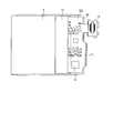
図2に示すように、液晶表示装置100の画像表示面側で、その一端部10aがパネル基板1に接続されたフレキシブル基板10は、ベゼル9の側面に位置する折り返し部10bを経て、ベゼル9の背面側に折り返されている。フレキシブル基板10の一端部10aとは反対側の他端部10cは、ベゼル9の一部を覆うような形状となっていて、この他端部10cでベゼル9の背面に固着されている。
ベゼル9の背面には、液晶パネル3で表示される画像信号を処理する信号回路や、ベゼル9に内蔵されるバックライト8の駆動回路などが搭載された、背面回路基板12が配置されていて、フレキシブル基板10の他端部10cは、この背面回路基板12に接続されている。
また、フレキシブル基板10の他端部10cには、半導体チップやコンデンサなどの回路素子13が配置されている。図2に示す例では、これらの回路素子13は、フレキシブル基板10の他端部10c上に直接搭載された、TCP(Tape Carrier Package)技術が採用されているが、回路素子13をポリカーボネートなどの硬質樹脂基板上に搭載し、この硬質樹脂基板をフレキシブル基板10上に固着してもよい。
フレキシブル基板10の折り返し部10bの外側表面には、変形防止材11が塗布されている。この変形防止材11については、後に詳述する。
液晶表示装置100は、外部から所定の電源と信号を入力するだけで、画像表示を行うことができる、ひとまとまりの電気回路構造体であるモジュールとして作成されていて、液晶表示装置100全体の制御を行うための半導体集積回路が形成される制御部14を有している。本実施形態の液晶表示装置100では、制御部14は、フレキシブル基板10の他端部10cから延長された部分として形成されている。
フレキシブル基板10の折り返し部10bに形成された変形防止材11は、フレキシブル基板10を折り返した状態で、紫外線または室温以上の熱により硬化されたものである。
変形防止材11としては、塗布のしやすさやフレキシブル基板10の材料との相性、フレキシブル基板や液晶パネルなどに悪影響のない条件で硬化できること、硬化後の強靱性や柔軟性などの観点から適宜選択すればよい。なお、変形防止材11の硬化後の良好な強度としては、硬度(シェアD:ASTM D7720)が70程度のものが目安となる。
例えば、紫外線硬化性材料を用いる場合には、紫外線によって速く硬化し、強靱性と柔軟性を併せ持つ、ポリウレタンメタクリレート樹脂を基材とする材料が好ましい。具体的には、ヘンケル・ジャパン株式会社製の「ロックタイト(LOCTITE)3523UV」(製品名)などが使用できる。このような、ポリウレタンメタクリレート樹脂を基材とする嫌気性接着剤であれば、室温環境下、紫外線の照射のみでの硬化が可能であるため、フレキシブル基板10や周囲に配置される電気回路素子に対して、変形防止材11を硬化させる際の環境条件によって悪影響を与えてしまうことを防止することができる。上記以外にも、ポリウレタンメタクリレート樹脂と同等の強靱性と柔軟性とを併せ持つ材料を選択することで、振動や衝撃に高い耐性を示す変形防止材11とすることができる。
また、熱硬化性材料を用いる場合には、例えば、2液混合タイプのエポキシ樹脂製接着剤が、十分な強度を有するという点で好ましい。具体的には、ヘンケル・ジャパン株式会社製の「E-40FL」(製品名)などを使用することができる。
変形防止材11のフレキシブル基板10への塗布手段や条件については、上記した室温硬化タイプの材料の場合などで塗布後硬化までの時間が限られているものを除き、特別な制約はない。したがって、フレキシブル基板10単体で、折り返し部10bを所定の湾曲状態とした後に塗布することも可能であり、また、フレキシブル基板10の一端部10aをパネル基板1の実装領域6に固着した状態で、フレキシブル基板10を折り返し部10bで折り返した後でもかまわない。さらには、フレキシブル基板10の一端部10aをパネル基板1の実装領域6に、他端部10cをベゼル9の背面にそれぞれ固着した後に、変形防止材11を塗布するようにしてもよい。
なお、変形防止材11は、フレキシブル基板10の折り返し部11bの外表面に正確に塗布することが効果的であるから、フレキシブル基板10の一端部10aをパネル基板1に固着後、少なくとも折り返し部10bで仮止めしたような、所定の形状に折り返した状態で塗布することがより好ましい。
変形防止材11のフレキシブル基板10への塗布方法としては、刷毛塗りやスプレーコート法、転写法、印刷法など、溶液またはゲル状物を所定面積に塗布する一般的な方法が適用できる。中でも刷毛塗り法は、変形防止材11を所定領域に簡易に塗布できる方法として最も好ましい。
変形防止材11の塗布領域としては、フレキシブル基板10の折り返し部10bの外側の一部または全体に塗布することができるが、折り返し部10bの外側表面全体に塗布することが好ましい。また、塗布厚さについては、フレキシブル基板10の反発力を抑えることができる範囲で適宜選択できる。一例として、紫外線硬化型の嫌気性樹脂接着剤を刷毛塗りで塗布する場合には、塗布厚さ0.2mm~2.0mm程度の範囲で適宜選択される。なお、塗布厚さは、均一であることがより好ましいが、塗布される領域で所定の最低限度の厚さが確保できれば、それほどの厳密性は要求されない。
さらに、フレキシブル基板10への変形防止材の塗布は、直接塗布する方法に限られず、他の媒介を介して塗布することもできる。例えば、フレキシブル基板10上での塗布部分形状に合わせたテープ状部材の表面に、変形防止材11を塗布したものを作成し、このテープ状部材をフレキシブル基板10に貼着する方法も利用できる。なお、この場合には、変形防止材11を硬化させる時や、液晶表示装置の実使用時に、剥がれが生じないテープを選択すべきであることは言うまでもない。テープ状部材の基材としては、例えば厚さが0.1mm~0.2mm程度の不繊布テープが利用でき、このようなテープ状部材に、上記した刷毛塗り法などを用いて、変形防止材11を塗布することができる。
また、フレキシブル基板10の反発力を抑える度合いとしては、必ずしも100%の抑制力、すなわち、フレキシブル基板10が全く変形しない状態にまで押さえ込む必要はなく、50%程度以上の抑制力があれば十分であると考えられる。本発明の変形防止材11は、両端部が固着されたフレキシブル基板10の変形を抑えるものだからである。
なお、本明細書において100%の抑制力とは、フレキシブル基板10の両端部が並行になる状態まで曲げた状態で変形防止材11を塗布し、フレキシブル基板10を抑えていた力を解放しても、変形防止材11がその変形状態を保つことができるものをいう。また、50%の抑制力とは、フレキシブル基板10を抑えていた力を解放したときに、フレキシブル基板10の両端部が開いて、その間隔が平行な状態での間隔の2倍となった状態のものをいう。このように、変形防止材11の抑制力が50%程度で足りる場合には、変形防止材11の必要塗布量を減らすことができる。
図3および図4は、変形防止材11によるフレキシブル基板10の反発力抑制効果を確認する確認試験方法を示す図である。
図3は、測定対象の変形防止材11の塗布状態の例を示し、図4は、変形防止材11による反発力抑制効果の測定の様子を示す。
図3に示すように、例えば、幅10mm、長さ40mmのフレキシブル基板10を用意し、フレキシブル基板10の両端をクリップ21で固定する。そして、フレキシブル基板10の中間部分の湾曲している部分の外側表面に、変形防止材11を塗布する。なお、塗布領域は、フレキシブル基板10の長さ方向に対して、縦長に塗布するものと、横長に塗布するものとの2種類を作成する。
図3(a)に示す、フレキシブル基板10の長さ方向に対して縦長に塗布した場合は、図3(a)中にaとして示す塗布幅が3mmで、塗布長さが5mmとする。また、図3(b)に示す、フレキシブル基板10の長さ方向に対して横長に塗布した場合は、図3(b)中にbとして示す塗布幅が3mmで、塗布長さが5mmとする。なお、塗布厚さは、例えば2mmとするなど均一に塗布する。
変形防止材11の硬化条件は、使用する変形防止材11の材質を考慮して、適宜好ましい硬化条件を策定する。例えば、紫外線硬化性材料の場合は、照射する紫外線の波長と強度、照射時間を定める。具体的には、波長365nmの光を100mW/cm2の強さで15秒間照射するなどである。また、熱硬化性材料の場合は、硬化温度と硬化時間を定める。例えば、温度80℃で30分の硬化を行うなどである。
これらの実験結果の評価方法としては、変形防止材11を硬化させた後にフレキシブル基板10を固定していたクリップ21を外し、このときの、フレキシブル基板10の両端部の間隔を測定することが考えられる。具体的には、図4(a)に示すように、フレキシブル基板10の反発力が抑えられ、フレキシブル基板10の両端部がほぼ並行になった状態での両端部の間隔cを基準として、それぞれの測定試料について、実際にフレキシブル基板10の両端部の間隔dを測定する。例えば、フレキシブル基板10の先端部がほぼ並行であるときの間隔cが5mmであるときに、測定試料の変形防止材11を用いた場合のフレキシブル基板10の先端部の間隔dが、5mmであれば反発抑制力が100%、10mmであれば反発抑制力が50%と評価することが考えられる。
以上説明したように、本実施形態の液晶表示装置100では、フレキシブル基板10の折り返し部10bの外側表面に変形防止材11を塗布し、フレキシブル基板10を折り返した状態で硬化させることによって、フレキシブル基板10の折り返し部10bの反発力を効果的に抑えることができる。このため、ベゼル9背面に固着された、フレキシブル基板10の他端部10cが剥離するという問題を解消することができる。
なお、本実施形態の液晶表示装置の説明において、フレキシブル基板10の折り返し部10bを、一つの円弧を描くような形状とした場合について図示して説明したが、本発明はこれに限られず、フレキシブル基板10を機構部材であるベゼル9の側面に密着するように、すなわち、ベゼル9の側面の上端部と下端部とに、ほぼ直角に折り曲がる2つの折り曲げ部分を有し、この2つの折り曲げ部分の間がほぼ平面状となるような折り返し部とすることもできる。この場合には、変形防止材11を、2つの折り曲げ部分とベゼル9の側面に沿う平面状部分との、折り返し部全体に塗布することもできるし、2つの折り曲げ部分にのみ塗布することもできる。いずれの場合であっても、変形防止部材11によって、フレキシブル基板10の折り返し部の反発力を抑制し、フレキシブル基板10がベゼル9背面から剥離してしまうという問題を、効果的に防止することができる。
本発明は、回路基板に接続されたフレキシブル基板が折り返し部で折り返されて機構部材の背面に固着される電気回路構造体として、液晶表示装置をはじめ各種用途に産業上利用可能である。
Claims (5)
- 有底枠状の機構部材と、
前記機構部材内に収容される、表面に電気回路素子が形成された回路基板と、
一端部に形成された接続端子が、前記回路基板上に形成された電極端子に接続されるとともに、前記機構部材の側面で折り返し部により折り返され、前記一端部の反対側の他端部が前記機構部材の背面に固着されたフレキシブル基板とを備え、
前記フレキシブル基板の前記折り返し部の外側表面に、前記フレキシブル基板を折り返した状態で紫外線または室温以上の熱により硬化された、変形防止材が塗布されていることを特徴とする電気回路構造体。 - 前記変形防止材が、ポリウレタンメタクリケート樹脂を主成分とする紫外線硬化性樹脂である請求項1記載の電気回路構造体。
- 前記変形防止材が、エポキシ系の熱硬化性樹脂である請求項1記載の電気回路構造体。
- 前記変形防止材が、テープ状部材に塗布され、前記テープ状部材が前記フレキシブル基板に貼着されている請求項1~3のいずれか1項に記載の電気回路構造体。
- 前記電気回路構造体が液晶表示装置であり、
前記回路基板が、液晶層を挟んで所定間隔を隔てて固着された対向基板と液晶パネルを構成するパネル基板である、請求項1から4のいずれか1項に記載の電気回路構造体。
Priority Applications (2)
| Application Number | Priority Date | Filing Date | Title |
|---|---|---|---|
| US13/056,993 US20110157536A1 (en) | 2008-08-11 | 2009-07-31 | Electric circuit structure |
| CN2009801297794A CN102113420A (zh) | 2008-08-11 | 2009-07-31 | 电路构造体 |
Applications Claiming Priority (2)
| Application Number | Priority Date | Filing Date | Title |
|---|---|---|---|
| JP2008207185 | 2008-08-11 | ||
| JP2008-207185 | 2008-08-11 |
Publications (1)
| Publication Number | Publication Date |
|---|---|
| WO2010018756A1 true WO2010018756A1 (ja) | 2010-02-18 |
Family
ID=41668900
Family Applications (1)
| Application Number | Title | Priority Date | Filing Date |
|---|---|---|---|
| PCT/JP2009/063683 Ceased WO2010018756A1 (ja) | 2008-08-11 | 2009-07-31 | 電気回路構造体 |
Country Status (3)
| Country | Link |
|---|---|
| US (1) | US20110157536A1 (ja) |
| CN (1) | CN102113420A (ja) |
| WO (1) | WO2010018756A1 (ja) |
Families Citing this family (9)
| Publication number | Priority date | Publication date | Assignee | Title |
|---|---|---|---|---|
| JP6125264B2 (ja) * | 2013-02-19 | 2017-05-10 | 京セラ株式会社 | フレキシブルリード基板を内蔵した電子機器 |
| US9107316B2 (en) * | 2013-09-11 | 2015-08-11 | Eastman Kodak Company | Multi-layer micro-wire substrate structure |
| CN104934550A (zh) * | 2015-05-07 | 2015-09-23 | 京东方科技集团股份有限公司 | Oled器件的封装结构、封装方法以及电子设备 |
| DE102015113928A1 (de) * | 2015-08-21 | 2017-02-23 | Schreiner Group Gmbh & Co. Kg | Gegenstand mit einer elektronischen Einheit und mit Leiterstrukturen auf einer Trägerstruktur |
| KR102378357B1 (ko) * | 2015-08-24 | 2022-03-25 | 삼성디스플레이 주식회사 | 폴딩 가능한 디스플레이 장치 및 그 운용방법 |
| CN106585069A (zh) * | 2016-12-23 | 2017-04-26 | 武汉华星光电技术有限公司 | 柔性基板、面板及丝网印刷机制作柔性基板、面板的方法 |
| JP2019012719A (ja) * | 2017-06-29 | 2019-01-24 | 株式会社Joled | フレキシブル配線板、及び、表示装置 |
| CN108601222B (zh) * | 2018-04-18 | 2019-09-17 | 霸州市云谷电子科技有限公司 | 柔性电路板翻折装置 |
| CN113731746B (zh) * | 2020-05-27 | 2022-11-25 | 京东方科技集团股份有限公司 | 翻折装置 |
Citations (5)
| Publication number | Priority date | Publication date | Assignee | Title |
|---|---|---|---|---|
| JPH05129748A (ja) * | 1991-10-31 | 1993-05-25 | Sharp Corp | 回路基板 |
| JP2004063691A (ja) * | 2002-07-26 | 2004-02-26 | Optrex Corp | 可撓配線基板およびその折り曲げ形成方法 |
| JP2006098811A (ja) * | 2004-09-30 | 2006-04-13 | Optrex Corp | 表示装置 |
| JP2007134473A (ja) * | 2005-11-10 | 2007-05-31 | Matsushita Electric Ind Co Ltd | フレキシブル配線基板およびその製造方法 |
| JP2007206252A (ja) * | 2006-01-31 | 2007-08-16 | Optrex Corp | 表示体用枠体 |
-
2009
- 2009-07-31 WO PCT/JP2009/063683 patent/WO2010018756A1/ja not_active Ceased
- 2009-07-31 US US13/056,993 patent/US20110157536A1/en not_active Abandoned
- 2009-07-31 CN CN2009801297794A patent/CN102113420A/zh active Pending
Patent Citations (5)
| Publication number | Priority date | Publication date | Assignee | Title |
|---|---|---|---|---|
| JPH05129748A (ja) * | 1991-10-31 | 1993-05-25 | Sharp Corp | 回路基板 |
| JP2004063691A (ja) * | 2002-07-26 | 2004-02-26 | Optrex Corp | 可撓配線基板およびその折り曲げ形成方法 |
| JP2006098811A (ja) * | 2004-09-30 | 2006-04-13 | Optrex Corp | 表示装置 |
| JP2007134473A (ja) * | 2005-11-10 | 2007-05-31 | Matsushita Electric Ind Co Ltd | フレキシブル配線基板およびその製造方法 |
| JP2007206252A (ja) * | 2006-01-31 | 2007-08-16 | Optrex Corp | 表示体用枠体 |
Also Published As
| Publication number | Publication date |
|---|---|
| US20110157536A1 (en) | 2011-06-30 |
| CN102113420A (zh) | 2011-06-29 |
Similar Documents
| Publication | Publication Date | Title |
|---|---|---|
| WO2010018756A1 (ja) | 電気回路構造体 | |
| CN101393329B (zh) | 一种装置及其制造方法 | |
| US8035789B2 (en) | Mounting structure, electro-optical device, input device, method of manufacturing mounting structure, and electronic apparatus | |
| KR101001405B1 (ko) | 액정표시장치 | |
| US9989793B2 (en) | Display device | |
| KR101797001B1 (ko) | 이방성 도전필름, 이를 이용한 표시패널의 제조방법 및 그 표시패널을 포함하는 평판표시장치모듈 | |
| JP4178968B2 (ja) | バックライトユニット、電気光学装置、電子機器、バックライトユニットの製造方法、および電気光学装置の製造方法 | |
| KR101294850B1 (ko) | 액정표시장치 | |
| JP2009186971A (ja) | 電気光学装置及び電子機器 | |
| JP2005266284A (ja) | 電気光学装置の製造方法、その製造方法で製造した電気光学装置を搭載した電子機器、および偏光板 | |
| KR102253430B1 (ko) | 표시 장치 | |
| JP5053438B2 (ja) | 電気回路構造体 | |
| KR101292569B1 (ko) | 액정표시소자 | |
| US10969632B2 (en) | Display panel and method of processing the same | |
| KR20100071533A (ko) | 백라이트 유닛 및 이를 구비한 액정표시장치 | |
| JP4760571B2 (ja) | 液晶装置、照明装置及び電子機器 | |
| JP3719362B2 (ja) | 表示装置および電子機器 | |
| KR20060084558A (ko) | 평판표시패널의 유동을 방지하는 평판표시장치 | |
| KR101313649B1 (ko) | 액정표시소자 | |
| KR20060084015A (ko) | 인쇄회로기판 보호용 커버를 부착한 평판표시장치 및 그제조 방법 | |
| KR20080001510A (ko) | 액정표시소자 | |
| WO2019013115A1 (ja) | 表示装置 | |
| KR101174152B1 (ko) | 액정표시모듈 | |
| JP4432549B2 (ja) | 電気光学装置及び電子機器 | |
| KR20080001503A (ko) | 액정표시소자 |
Legal Events
| Date | Code | Title | Description |
|---|---|---|---|
| WWE | Wipo information: entry into national phase |
Ref document number: 200980129779.4 Country of ref document: CN |
|
| 121 | Ep: the epo has been informed by wipo that ep was designated in this application |
Ref document number: 09806649 Country of ref document: EP Kind code of ref document: A1 |
|
| NENP | Non-entry into the national phase |
Ref country code: DE |
|
| NENP | Non-entry into the national phase |
Ref country code: JP |
|
| 122 | Ep: pct application non-entry in european phase |
Ref document number: 09806649 Country of ref document: EP Kind code of ref document: A1 |