WO2010013693A1 - 光半導体素子、光電変換素子及び光変調素子 - Google Patents
光半導体素子、光電変換素子及び光変調素子 Download PDFInfo
- Publication number
- WO2010013693A1 WO2010013693A1 PCT/JP2009/063394 JP2009063394W WO2010013693A1 WO 2010013693 A1 WO2010013693 A1 WO 2010013693A1 JP 2009063394 W JP2009063394 W JP 2009063394W WO 2010013693 A1 WO2010013693 A1 WO 2010013693A1
- Authority
- WO
- WIPO (PCT)
- Prior art keywords
- type
- semiconductor layer
- semiconductor
- optical
- layer
- Prior art date
- Legal status (The legal status is an assumption and is not a legal conclusion. Google has not performed a legal analysis and makes no representation as to the accuracy of the status listed.)
- Ceased
Links
Images




Classifications
-
- H—ELECTRICITY
- H10—SEMICONDUCTOR DEVICES; ELECTRIC SOLID-STATE DEVICES NOT OTHERWISE PROVIDED FOR
- H10F—INORGANIC SEMICONDUCTOR DEVICES SENSITIVE TO INFRARED RADIATION, LIGHT, ELECTROMAGNETIC RADIATION OF SHORTER WAVELENGTH OR CORPUSCULAR RADIATION
- H10F30/00—Individual radiation-sensitive semiconductor devices in which radiation controls the flow of current through the devices, e.g. photodetectors
- H10F30/20—Individual radiation-sensitive semiconductor devices in which radiation controls the flow of current through the devices, e.g. photodetectors the devices having potential barriers, e.g. phototransistors
- H10F30/21—Individual radiation-sensitive semiconductor devices in which radiation controls the flow of current through the devices, e.g. photodetectors the devices having potential barriers, e.g. phototransistors the devices being sensitive to infrared, visible or ultraviolet radiation
- H10F30/22—Individual radiation-sensitive semiconductor devices in which radiation controls the flow of current through the devices, e.g. photodetectors the devices having potential barriers, e.g. phototransistors the devices being sensitive to infrared, visible or ultraviolet radiation the devices having only one potential barrier, e.g. photodiodes
- H10F30/223—Individual radiation-sensitive semiconductor devices in which radiation controls the flow of current through the devices, e.g. photodetectors the devices having potential barriers, e.g. phototransistors the devices being sensitive to infrared, visible or ultraviolet radiation the devices having only one potential barrier, e.g. photodiodes the potential barrier being a PIN barrier
-
- H—ELECTRICITY
- H10—SEMICONDUCTOR DEVICES; ELECTRIC SOLID-STATE DEVICES NOT OTHERWISE PROVIDED FOR
- H10F—INORGANIC SEMICONDUCTOR DEVICES SENSITIVE TO INFRARED RADIATION, LIGHT, ELECTROMAGNETIC RADIATION OF SHORTER WAVELENGTH OR CORPUSCULAR RADIATION
- H10F77/00—Constructional details of devices covered by this subclass
- H10F77/10—Semiconductor bodies
- H10F77/12—Active materials
- H10F77/122—Active materials comprising only Group IV materials
-
- Y—GENERAL TAGGING OF NEW TECHNOLOGICAL DEVELOPMENTS; GENERAL TAGGING OF CROSS-SECTIONAL TECHNOLOGIES SPANNING OVER SEVERAL SECTIONS OF THE IPC; TECHNICAL SUBJECTS COVERED BY FORMER USPC CROSS-REFERENCE ART COLLECTIONS [XRACs] AND DIGESTS
- Y02—TECHNOLOGIES OR APPLICATIONS FOR MITIGATION OR ADAPTATION AGAINST CLIMATE CHANGE
- Y02E—REDUCTION OF GREENHOUSE GAS [GHG] EMISSIONS, RELATED TO ENERGY GENERATION, TRANSMISSION OR DISTRIBUTION
- Y02E10/00—Energy generation through renewable energy sources
- Y02E10/50—Photovoltaic [PV] energy
- Y02E10/547—Monocrystalline silicon PV cells
Definitions
- the present invention relates to an optical semiconductor device having a PIN structure using an i-type (intrinsic) Si x Ge 1-x semiconductor, and more particularly to an optical semiconductor device having a low dark current.
- a Ge-PIN photoelectric conversion element on a Si semiconductor integrated circuit there is one in which an i-type Ge semiconductor layer is formed as an absorption layer between a p-type Si semiconductor layer and an n-type Si semiconductor layer.
- a conventional photoelectric conversion element 10 as shown in FIG. 1A is formed by epitaxial growth by a p-type Si semiconductor layer 11 indicated as p-Si in the figure and an i-type Ge semiconductor layer indicated as i-Ge. 12 and an n-type Si semiconductor layer 13 described as n-Si are stacked in order from the substrate to form a PIN structure.
- the photoelectric conversion element 10 having the PIN structure generates a photovoltaic current when irradiated with light from above through a space.
- the photoelectric conversion element 10 is irradiated with light from a lateral direction or a downward direction, and generates a photovoltaic current.
- the content of Ge atoms in the amorphous silicon germanium constituting the i-type layer is in the range of 20 to 70 atomic%, and the Ge atom content is distributed so as to have a maximum value in the stacking direction.
- the non-single-crystal silicon buffer layer not containing Ge atoms is provided on the side in contact with the p-type layer and the n-type layer.
- the bandgap is narrower than that of a Si semiconductor and is forbidden than the wavelength of propagating light. It is necessary to use a Ge (germanium) semiconductor having a wide band width.
- a Ge-PIN optical modulation element on an Si semiconductor integrated circuit an i-type Ge semiconductor layer propagates between a p-type Si semiconductor layer and an n-type Si semiconductor layer between an external voltage of 0 V and a specific voltage Vo. Some are formed so as to act as a light transmission or absorption layer. This is called an electroabsorption type light modulation element.
- a conventional light modulation element 10 as shown in FIG. 1A is formed by epitaxial growth, a p-type Si semiconductor layer 11 indicated as p-Si in the figure, and an i-type Ge semiconductor layer indicated as i-Ge. 12 and an n-type Si semiconductor layer 13 described as n-Si are stacked in order from the substrate to form a PIN structure.
- the light modulator 10 having a PIN structure absorbs light when an external voltage is applied when light is irradiated from above through a space, and transmits light when the external voltage is removed.
- the light modulation element 10 absorbs light when an external voltage is applied when light is irradiated from the lateral direction or the downward direction, and light is removed when the external voltage is removed. Permeate.
- Non-Patent Document 1 There is a light modulation device described in Non-Patent Document 1 as this type of light modulation element.
- This light modulation device is configured such that the content of Ge atoms in silicon germanium constituting the i-type layer is in the range of 20 to 95 atomic%.
- the photoelectric conversion element or the light modulation element 10 shown in FIG. 1A when a Ge semiconductor layer is stacked, a lattice mismatch occurs between the Si semiconductor layer and the Ge semiconductor layer. A lattice defect generated by this lattice mismatch causes dark current.
- the epitaxial growth of the Si semiconductor is usually performed at 650 ° C. or lower. It is not preferable to perform a high-temperature annealing treatment at 700 to 900 ° C. during the Si semiconductor lamination process.
- the p-type Si semiconductor layer and the n-type Si semiconductor layer that are adjacent to each other on both sides of the i-type Ge semiconductor layer cause the both sides of the i-type Ge semiconductor layer to become a p-type Ge semiconductor layer and an n-type Ge semiconductor layer, respectively.
- a PIN structure is formed in the Ge semiconductor layer itself.
- a p-type Ge semiconductor layer 12a is generated at the interface between the p-type Si semiconductor layer 11 and the i-type Ge semiconductor layer 12, and an n-type Si semiconductor layer 13 is formed.
- an i-type Ge semiconductor layer 12 are formed with an n-type Ge semiconductor layer 12b. That is, since the p-type and the n-type are formed on both sides in the i-type Ge semiconductor layer 12, the Ge semiconductor layer itself has a PIN structure.
- the present invention reduces an electric field applied to an optical functional layer in an optical semiconductor element having an optical functional layer between a p-type Si semiconductor layer and an n-type Si semiconductor layer. Objective.
- the present invention prevents a PIN structure from being formed in the SiGe semiconductor layer and reduces the electric field applied to the SiGe semiconductor layer itself in the SiGe-PIN optical semiconductor element. With the goal.
- the optical semiconductor element of the present invention has an optical functional layer and an electric field control layer sandwiched between a p-type Si semiconductor layer and an n-type Si semiconductor layer.
- the optical semiconductor element of the present invention is an optical semiconductor element comprising an optical functional layer and an electric field control layer, and the optical functional layer and the electric field are interposed between a p-type Si semiconductor layer and an n-type Si semiconductor layer.
- the optical semiconductor element is characterized in that the control layer is sandwiched.
- the optical functional layer sandwiched between the p-type Si semiconductor layer and the n-type Si semiconductor layer exhibits the function of the optical semiconductor element, and the electric field control layer prevents the electric field from being applied to the optical functional layer. be able to.
- the optical functional layer has an i-type Si x Ge 1-x semiconductor layer (where 0 ⁇ x ⁇ 0.6). A semiconductor element was obtained.
- This configuration can secure use in a long wavelength band by containing Ge 40% or more.
- the optical semiconductor element is characterized in that the electric field control layer has an i-type Si semiconductor layer.
- i-type Si x Ge 1-x for i-type Si semiconductor layer is disposed between the semiconductor layer and the p-type Si semiconductor layer, p-type Si semiconductor i-type Si x Ge 1-x semiconductor layer It can be avoided that the side close to the layer side becomes p-type.
- this structure since the i-type Si semiconductor layer is disposed between the i-type Si x Ge 1-x semiconductor layer and the n-type Si semiconductor layer, n-type of the i-type Si x Ge 1-x semiconductor layer It can be avoided that the side close to the Si semiconductor layer side becomes n-type. For this reason, this structure can prevent the PIN structure from being formed in the Si x Ge 1-x semiconductor layer itself. That is, this structure can prevent an electric field from being applied to the Si x Ge 1-x semiconductor layer.
- the electric field control layer is a semiconductor of any one of an n-type Si semiconductor layer, an n-type Ge semiconductor layer, and an n-type SiGe semiconductor layer between the optical functional layer and the i-type Si semiconductor layer.
- An optical semiconductor element characterized by further having a layer.
- the side near the i-type Si semiconductor layer of the i - type Si x Ge 1-x semiconductor layer is likely to be p-type.
- an electric field is applied to the SiGe semiconductor layer as in the conventional case, and dark current increases.
- the optical semiconductor element of the present invention uses an i-type Si x Ge 1-x semiconductor layer (where 0 ⁇ x ⁇ 0.6) as a reaction region, and the i-type Si x Ge 1
- the i-type Si semiconductor layer is arranged between the 1-x semiconductor layer and the n-type Si semiconductor layer or the p-type Si semiconductor layer.
- the optical semiconductor device of the present invention includes a p-type Si semiconductor layer, an i-type Si x Ge 1-x semiconductor layer (where 0 ⁇ x ⁇ 0.6), an i-type Si semiconductor layer, and an n-type Si.
- the optical semiconductor element is characterized in that the semiconductor layers are sequentially stacked.
- the i - type Si semiconductor layer is disposed between the i - type Si x Ge 1-x semiconductor layer and the n-type Si semiconductor layer. For this reason, this structure can avoid the side near the n-type Si semiconductor layer side of the i-type Si x Ge 1-x semiconductor layer from becoming n-type, and a PIN structure is formed in the Ge semiconductor layer itself. Can be prevented. In addition, this structure can ensure use in a long wavelength band by including 40% or more of Ge in the i-type Si x Ge 1-x semiconductor layer.
- the optical semiconductor element of the present invention includes an n-type Si semiconductor layer, an i-type Si x Ge 1-x semiconductor layer (where 0 ⁇ x ⁇ 0.6), an i-type Si semiconductor layer, p An optical semiconductor element characterized in that type Si semiconductor layers are sequentially laminated.
- the i - type Si semiconductor layer is disposed between the i - type Si x Ge 1-x semiconductor layer and the p-type Si semiconductor layer. Therefore, this structure can avoid the p-type Si side of the i-type Si x Ge 1-x semiconductor layer close to the p-type Si semiconductor layer side, and the Si x Ge 1-x semiconductor layer itself has a PIN structure. Can be prevented from being formed. In addition, this structure can ensure use in a long wavelength band by including 40% or more of Ge in the i-type Si x Ge 1-x semiconductor layer.
- the optical semiconductor element of the present invention is the above optical semiconductor element, wherein an n-type Si semiconductor layer, an n-type Ge semiconductor layer, and an n-type Si semiconductor layer are interposed between the i-type Si x Ge 1-x semiconductor layer and the i-type Si semiconductor layer. It is desirable to have any one of the type SiGe semiconductor layers.
- the side near the i-type Si semiconductor layer of the i - type Si x Ge 1-x semiconductor layer is likely to be p-type.
- an electric field is applied to the SiGe semiconductor layer as in the conventional case, and dark current increases.
- the optical semiconductor element of the present invention is the above-described optical semiconductor element, wherein the n-type Si semiconductor layer and the n-type Ge semiconductor layer are provided between the i-type Si x Ge 1-x semiconductor layer and the i-type Si semiconductor layer.
- the n-type carrier concentration of the n-type SiGe semiconductor layer is 10 11 cm ⁇ 2 or more and 10 14 cm ⁇ 2 or less.
- the n-type carrier concentration is about 10 14 cm ⁇ 2 as a limit value of doping.
- the i-type Si semiconductor layer has a thickness of 20 nm or more in the above-described optical semiconductor element.
- This configuration facilitates lattice matching between the i-type Si x Ge 1-x semiconductor layer and the n-type Si semiconductor layer or the p-type Si semiconductor layer.
- the photoelectric conversion element of the present invention is characterized in that a reverse bias of 0 V or more is applied to the above-described optical semiconductor element to convert an optical signal incident on the i-type Si x Ge 1-x semiconductor layer into an electrical signal. It is a photoelectric conversion element.
- This configuration can detect an optical signal with a wavelength of 0.8 to 1.6 ⁇ m. In addition, since this configuration has a small dark current, it is possible to detect an optical signal having a high S / N ratio.
- the light modulation element of the present invention controls the reverse bias of 0 V or more applied to the above-described optical semiconductor element, and makes the absorption rate variable with respect to the optical signal incident on the i-type Si x Ge 1-x semiconductor layer. This is a light modulation element.
- This configuration can modulate light with a wavelength of 0.8 to 1.6 ⁇ m.
- this configuration since this configuration has a small dark current, light can be modulated with low power consumption.
- the light modulation element of the present invention controls a reverse bias of 0 V or more applied to the above-described optical semiconductor element, and makes the refractive index variable with respect to the optical signal incident on the i-type Si x Ge 1-x semiconductor layer.
- a light modulation element controls a reverse bias of 0 V or more applied to the above-described optical semiconductor element, and makes the refractive index variable with respect to the optical signal incident on the i-type Si x Ge 1-x semiconductor layer.
- This configuration can modulate an optical signal having a wavelength of 0.8 to 1.6 ⁇ m.
- this configuration since this configuration has a small dark current, light can be modulated with low power consumption.
- the optical functional layer refers to a layer having any one of a photoelectric conversion function for converting light into electricity, an absorptivity variable function for varying a light absorption ratio, and a refractive index variable function for varying a refractive index with respect to light. .
- the electric field control layer refers to a layer between the optical functional layer and the n-type Si semiconductor layer or the p-type Si semiconductor layer and having a function of reducing the electric field applied to the optical functional layer.
- an i-type semiconductor refers to an intrinsic semiconductor that is not doped with impurities.
- An n-type semiconductor refers to a semiconductor that uses electrons as carriers, and a p-type semiconductor refers to a semiconductor that uses holes as carriers.
- the electric field applied to the optical functional layer can be reduced.
- the SiGe-PIN optical semiconductor element in the SiGe-PIN optical semiconductor element, it is possible to prevent the PIN structure from being formed in the SiGe semiconductor layer and to reduce the electric field applied to the SiGe semiconductor layer itself.
- (A) is a figure which shows the structure of the photoelectric conversion element of the conventional PIN structure.
- (B) is a figure which shows the structure of the photoelectric conversion element of the conventional PIN structure.
- (A) is a figure which shows the structure of the optical semiconductor element which concerns on embodiment of this invention.
- (B) is a figure which shows the structure of the optical semiconductor element which concerns on embodiment of this invention. It is a figure which shows the change of the forbidden bandwidth by the bias of the optical semiconductor element which concerns on embodiment of this invention.
- (A) is a figure which shows the change of a band width in the case of a structure without an i-type Si semiconductor layer.
- (B) is a figure which shows the change of a band width in the case of a structure with an i-type Si semiconductor layer.
- FIG. 6A is a diagram showing wavelength-sensitivity characteristics using the bias of the photoelectric conversion element according to the embodiment of the present invention as a parameter.
- FIG. 6B is a diagram showing wavelength-sensitivity characteristics using the bias of the photoelectric conversion element according to the embodiment of the present invention as a parameter. It is a figure explaining the mixed crystal ratio of the optical semiconductor element which concerns on embodiment of this invention.
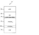
- the photoelectric conversion element 20 as the optical semiconductor element of this embodiment includes a p-type Si semiconductor layer 11 and an i-type Si x Ge 1-x semiconductor layer (provided that 0 ⁇ x ⁇ 0.6) 21, i-type Si semiconductor layer 22, and n-type Si semiconductor layer 23 are stacked in order from the substrate to form a PIN structure.
- a p-type Si semiconductor layer 11 and an i-type Si x Ge 1-x semiconductor layer (provided that 0 ⁇ x ⁇ 0.6) 21, i-type Si semiconductor layer 22, and n-type Si semiconductor layer 23 are stacked in order from the substrate to form a PIN structure.
- the p-type Si semiconductor layer 11 is described as p-Si
- the i-type Si x Ge 1-x semiconductor layer 21 is described as i-Si x Ge 1-x
- the i-type Si semiconductor layer 22 Is described as i-Si
- the n-type Si semiconductor layer 23 is described as n-Si.
- the photoelectric conversion element 20 is characterized in that, in the Ge-PIN structure shown in FIG. 1A, the upper n-type Si semiconductor layer 13 is replaced with an n-type Si semiconductor layer 23 and an i-type Si as shown in FIG.
- the semiconductor layer 22 has a two-layer structure.
- the thickness of the i-type Si x Ge 1-x semiconductor layer 21 is, for example, 500 nm to 30 ⁇ m. If the i-type Si x Ge 1-x semiconductor layer 21 has a thickness of 500 nm or more, it can effectively capture photons. On the other hand, the limit thickness at which a depletion layer is formed in the i-type Si x Ge 1-x semiconductor layer 21 is about 30 ⁇ m.
- the i-type Si semiconductor layer 22 has a thickness of 20 nm to 10 ⁇ m, for example. The i-type Si semiconductor is destroyed at 0.3 MeV / cm, and the forbidden band width of the Ge semiconductor is 0.6 V.
- the i-type Si semiconductor layer 22 has a thickness up to about 10 ⁇ m, the crystallinity uniformity of the i-type Si semiconductor can be sufficiently maintained by epitaxial growth.
- the thickness of the n-type Si semiconductor layer 23 is about 100 nm. This thickness can be formed by epitaxial growth and is sufficient as an electrode.
- the thickness of the p-type Si semiconductor layer 11 may be any thickness that can function as an electrode.
- the p-type Si semiconductor layer 11 may be laminated on the upper surface of the Si substrate, or the p-type Si semiconductor layer 11 may be formed by making the Si semiconductor substrate p-type by doping.
- the i-type Si semiconductor layer 22 and the i-type Si x Ge 1-x semiconductor layer 21 are thin in order to shorten the carrier transit time for detecting a high-speed optical signal, and efficiently capture photons in detecting a low-speed optical signal. To make it thicker.
- the photoelectric conversion element 20 having the PIN structure may be formed only by epitaxial growth without performing high-temperature annealing at 700 to 900 ° C. as in the prior art. Epitaxial growth is usually performed at 650 ° C. or lower, and the temperature is not further raised during this process. Further, a doping material such as B (boron) is selected as the doping material of the p-type Si semiconductor layer 11, and P (phosphorus), As (arsenic), Sb (as the doping material of the n-type Si semiconductor layer 23 is selected. Antimony) or the like is selected.
- B boron
- P phosphorus
- As arsenic
- Sb as the doping material of the n-type Si semiconductor layer 23
- Antimony or the like is selected.
- the photoelectric conversion element 20 may be manufactured without the need for high-temperature annealing as described above, but as shown in FIG. 2B, the p - type of the i-type Si x Ge 1-x semiconductor layer 21 is formed in the epitaxial growth process. on the side of the Si semiconductor layer 11, to form the p-Si x Ge 1-x p -type was described as Si x Ge 1-x semiconductor layer 21a. This is because the i-type Si x Ge 1-x is affected by the doping material doped in the p-type Si semiconductor layer 11 and becomes p-type Si x Ge 1-x due to thermal diffusion. On the other hand, the i-type Si x Ge 1-x semiconductor layer 21 on the i-type Si semiconductor layer 22 side is not affected by the doping material because the i-type Si semiconductor layer 22 is intrinsic.
- this photoelectric conversion element can avoid the i-type Si x Ge 1-x semiconductor layer 21 from becoming n-type on the i-type Si semiconductor layer 22 side, and the i-type Si x Ge 1- x 1 ⁇ It is possible to prevent the PIN structure from being formed in the x semiconductor layer 21.
- the i-type Si x Ge 1-x semiconductor layer (where x 0) 21 and the p-type Si semiconductor layer 11 (in FIG. 2B, p-type Si x Ge).
- the photoelectric conversion element of this embodiment may be an i-type Si p Ge 1-p semiconductor layer (0.5 ⁇ p ⁇ x) instead of the i-type Si semiconductor layer 22 in FIG. From the viewpoint of reducing lattice mismatch with the n-type Si semiconductor layer 23, p ⁇ x is desirable. On the other hand, in order to suppress the generation of dark current due to application of an electric field, it is necessary to increase the band gap. From this viewpoint, 0.5 ⁇ p is desirable.
- FIG. 3A shows a model in which a p-type Si semiconductor layer, an i-type Si x Ge 1-x semiconductor layer, and an n-type Si semiconductor layer are sequentially stacked.
- FIG. 3B shows a p-type Si semiconductor layer. , An i-type Si x Ge 1-x semiconductor layer, an i-type Si semiconductor layer, and an n-type Si semiconductor layer are sequentially stacked.
- FIG. 3A without the i-type Si semiconductor layer even when the external bias voltage is 0V, a potential difference occurs in the i-type Si x Ge 1-x semiconductor layer, and when the external bias voltage becomes 3V, the i-type Si x A large potential difference is generated in the Ge 1-x semiconductor layer.
- FIG. 3B having an i-type Si semiconductor layer when the external bias voltage is 0V, there is almost no potential difference in the i-type Si x Ge 1-x semiconductor layer, and even when the external bias voltage becomes 3V.
- the i-type Si x Ge 1-x semiconductor layer has a small potential difference.
- FIG. 4A shows a photoelectric conversion element (solid line in the figure) in which a p-type Si semiconductor layer, an i-type Si x Ge 1-x semiconductor layer, an n-type Si semiconductor layer are sequentially stacked, and a p-type Si semiconductor layer, This is a result of annealing a photoelectric conversion element (broken line in the figure) in which an i-type Si x Ge 1-x semiconductor layer, an i-type Si semiconductor layer, and an n-type Si semiconductor layer are sequentially laminated.
- FIG. 4B shows a photoelectric conversion element (solid line in the figure) and a p-type Si semiconductor layer in which a p-type Si semiconductor layer, an i-type Si x Ge 1-x semiconductor layer, an n-type Si semiconductor layer are sequentially stacked,
- This is a result of not subjecting the photoelectric conversion element (broken line in the figure) in which the i-type Si x Ge 1-x semiconductor layer, the i-type Si semiconductor layer, and the n-type Si semiconductor layer are sequentially laminated to the annealing treatment.
- the dark current is greatly increased by the application of an external bias when there is no i-type Si semiconductor layer, but the dark current is increased when there is an i-type Si semiconductor layer. It can be seen that it has been greatly suppressed.
- the increase in dark current can be largely suppressed whether or not there is an i-type Si semiconductor layer, and the dark current further increases in the case where there is an i-type Si semiconductor layer. It can be seen that it can be suppressed.
- FIG. 5 shows wavelength-sensitivity characteristics using an external bias applied to Ge-PIN as a parameter.
- FIG. 5A shows the result of annealing a photoelectric conversion element in which a p-type Si semiconductor layer, an i-type Si x Ge 1-x semiconductor layer, and an n-type Si semiconductor layer are sequentially laminated.
- FIG. 6 shows the relationship of the absorption coefficient ⁇ with respect to energy having x as a parameter. Assuming that light having a wavelength of 0.85 ⁇ m or more is detected, the wavelength of 0.85 ⁇ m is 1.45 eV as energy. At this time, when the absorption coefficient ⁇ is 1000 cm ⁇ 1 or more, x ⁇ 0.6. That is, it is understood that the Si ratio in the i-type Si x Ge 1-x semiconductor layer should be 0.6 or less in order to detect a wavelength of 0.85 ⁇ m or more.
- the SiGe-PIN photoelectric conversion element of this embodiment can prevent a PIN structure from being formed in the SiGe semiconductor layer itself, and as a result, application of an electric field to the SiGe semiconductor layer can be reduced.
- the light modulation element 20 as the optical semiconductor element of the present embodiment includes a p-type Si semiconductor layer 11 and an i-type Si x Ge 1-x semiconductor layer (provided that 0 ⁇ x ⁇ 0.6) 21, i-type Si semiconductor layer 22, and n-type Si semiconductor layer 23 are stacked in order from the substrate to form a PIN structure.
- a p-type Si semiconductor layer 11 and an i-type Si x Ge 1-x semiconductor layer (provided that 0 ⁇ x ⁇ 0.6) 21, i-type Si semiconductor layer 22, and n-type Si semiconductor layer 23 are stacked in order from the substrate to form a PIN structure.
- the p-type Si semiconductor layer 11 is described as p-Si
- the i-type Si x Ge 1-x semiconductor layer 21 is described as i-Si x Ge 1-x
- the i-type Si semiconductor layer 22 Is described as i-Si
- the n-type Si semiconductor layer 23 is described as n-Si.
- the light modulation element 20 is characterized in that, in the Ge-PIN structure shown in FIG. 1A, the upper n-type Si semiconductor layer 13 is replaced with an n-type Si semiconductor layer 23 and an i-type Si as shown in FIG.
- the semiconductor layer 22 has a two-layer structure.
- the thickness of the i-type Si x Ge 1-x semiconductor layer 21 is, for example, 200 nm to 10 ⁇ m. If the i-type Si x Ge 1-x semiconductor layer 21 has a thickness of 200 nm or more, the mode of light propagating through this layer can be set to a single mode. It can be propagated in a single mode. The above is the case of a channel waveguide. On the other hand, in the case of a rib waveguide, the i-type Si x Ge 1-x semiconductor layer 21 can be thickened to a thickness capable of propagating a single mode. The limit thickness at which the single mode of the rib waveguide is formed is about 10 ⁇ m.
- the i-type Si semiconductor layer 22 has a thickness of 20 nm to 10 ⁇ m, for example.
- the thickness of the n-type Si semiconductor layer 23 is about 100 nm. This thickness can be formed by epitaxial growth and is sufficient as an electrode.
- the thickness of the p-type Si semiconductor layer 11 may be any thickness that can function as an electrode.
- the p-type Si semiconductor layer 11 may be laminated on the upper surface of the Si substrate, or the p-type Si semiconductor layer 11 may be formed by making the Si semiconductor substrate p-type by doping.
- the i-type Si semiconductor layer 22 and the i-type Si x Ge 1-x semiconductor layer 21 are thinly stacked in order to shorten the resistance / capacitance product (charge / discharge time) for modulation of a high-speed optical signal.
- the i-type Si semiconductor layer 22 and the i-type Si x Ge 1-x semiconductor layer 21 need to have a thickness satisfying a single mode (about 100 nm in the channel waveguide).
- the light modulation element 20 having the PIN structure may be formed only by epitaxial growth without performing high-temperature annealing at 700 to 900 ° C. as in the prior art. Epitaxial growth is usually performed at 650 ° C. or lower, and the temperature is not further raised during this process. Further, a doping material such as B (boron) is selected as the doping material of the p-type Si semiconductor layer 11, and P (phosphorus), As (arsenic), Sb (as the doping material of the n-type Si semiconductor layer 23 is selected. Antimony) or the like is selected.
- B boron
- P phosphorus
- As arsenic
- Sb as the doping material of the n-type Si semiconductor layer 23
- Antimony or the like is selected.
- the light modulator 20 may be manufactured without the need for high-temperature annealing as described above.
- the p - type of the i-type Si x Ge 1-x semiconductor layer 21 is formed in the epitaxial growth process. on the side of the Si semiconductor layer 11, to form the p-Si x Ge 1-x p -type was described as Si x Ge 1-x semiconductor layer 21a. This is because the i-type Si x Ge 1-x is affected by the doping material doped in the p-type Si semiconductor layer 11 and becomes p-type Si x Ge 1-x due to thermal diffusion. On the other hand, the i-type Si x Ge 1-x semiconductor layer 21 on the i-type Si semiconductor layer 22 side is not affected by the doping material because the i-type Si semiconductor layer 22 is intrinsic.
- this light modulation element can avoid the i-type Si x Ge 1-x semiconductor layer 21 from becoming n-type on the i-type Si semiconductor layer 22 side, and i-type Si x Ge 1- 1 It is possible to prevent the PIN structure from being formed in the x semiconductor layer 21.
- the i-type Si x Ge 1-x semiconductor layer (where x 0) 21 and the p-type Si semiconductor layer 11 (in FIG. 2B, p-type Si x Ge).
- the light modulation element of this embodiment may be an i-type Si p Ge 1-p semiconductor layer (0.5 ⁇ p ⁇ x) instead of the i-type Si semiconductor layer 22 in FIG. From the viewpoint of reducing lattice mismatch with the n-type Si semiconductor layer 23, p ⁇ x is desirable. On the other hand, in order to suppress the generation of dark current due to application of an electric field, it is necessary to increase the band gap. From this viewpoint, 0.5 ⁇ p is desirable.
- FIG. 3A shows a model in which a p-type Si semiconductor layer, an i-type Si x Ge 1-x semiconductor layer, and an n-type Si semiconductor layer are sequentially stacked.
- FIG. 3B shows a p-type Si semiconductor layer. , An i-type Si x Ge 1-x semiconductor layer, an i-type Si semiconductor layer, and an n-type Si semiconductor layer are sequentially stacked.
- FIG. 3A without the i-type Si semiconductor layer even when the external bias voltage is 0 V, a potential difference is generated in the i-type Si x Ge 1-x semiconductor layer, which corresponds to 20 kV / cm. When the external bias voltage becomes 3V, a large potential difference is generated in the i-type Si x Ge 1-x semiconductor layer.
- FIG. 3B having an i-type Si semiconductor layer when the external bias voltage is 0V, there is almost no potential difference in the i-type Si x Ge 1-x semiconductor layer, and even when the external bias voltage becomes 3V.
- the i-type Si x Ge 1-x semiconductor layer has a small potential difference.
- the light modulation element can obtain a stronger FK (Franz-Keldysh) effect when the i-type Si semiconductor layer is present than the light modulation element without the i-type Si semiconductor layer. I understand.
- the FK effect means that when a DC electric field is applied to a semiconductor, the energy band of the conduction band and the valence band is inclined, and the wave function of electrons and holes oozes into the energy gap, so that the effective energy gap is The effect is smaller than the energy gap Eg when there is no electric field.
- FIG. 4A shows a light modulation element (solid line in the figure) and a p-type Si semiconductor layer in which a p-type Si semiconductor layer, an i-type Si x Ge 1-x semiconductor layer, an n-type Si semiconductor layer are sequentially stacked, FIG.
- FIG. 4B shows the result of annealing a light modulation element (broken line in the figure) in which an i-type Si x Ge 1-x semiconductor layer, an i-type Si semiconductor layer, and an n-type Si semiconductor layer are sequentially stacked.
- a p-type Si semiconductor layer, an i-type Si x Ge 1-x semiconductor layer, an n-type Si semiconductor layer stacked in this order (solid line in the figure) and a p-type Si semiconductor layer, i-type Si x Ge 1 This is a result of not annealing the light modulation element (broken line in the figure) in which the ⁇ x semiconductor layer, the i-type Si semiconductor layer, and the n-type Si semiconductor layer are sequentially stacked.
- the dark current is greatly increased by the application of an external bias when there is no i-type Si semiconductor layer, but the dark current is increased when there is an i-type Si semiconductor layer. It can be seen that it has been greatly suppressed.
- the increase in dark current can be largely suppressed whether or not there is an i-type Si semiconductor layer, and the dark current further increases in the case where there is an i-type Si semiconductor layer. It can be seen that it can be suppressed.
- FIG. 6 shows the relationship of the absorption coefficient ⁇ with respect to energy having x as a parameter. Assuming that light having a wavelength of 0.85 ⁇ m or more is modulated, the wavelength of 0.85 ⁇ m is 1.45 eV as energy. At this time, when the absorption coefficient ⁇ is 1000 cm ⁇ 1 or more, x ⁇ 0.6. That is, in order to modulate a wavelength of 0.85 ⁇ m or more, the i-type Si x Ge 1-x semiconductor layer may have a Si ratio of 0.6. Furthermore, as shown in the figure, since the light absorption increases as the electric field strength increases, an electroabsorption type light modulation element can be manufactured.
- FIG. 7 shows wavelength-absorption characteristics using an external bias applied to Ge-PIN as a parameter. As shown in FIG. 7, the absorption characteristics change greatly by controlling the magnitude of the bias. Therefore, it can be seen that the light modulation element in which the p-type Si semiconductor layer, the i-type Si x Ge 1-x semiconductor layer, the i-type Si semiconductor layer, and the n-type Si semiconductor layer are sequentially stacked can realize sufficient modulation.
- the light modulation element according to the present embodiment can not only modulate an optical signal by absorbing or transmitting an i-type Si x Ge 1-x semiconductor layer, but can also modulate an optical signal using a change in refractive index.
- the configuration of the Mach-Zehnder type modulator is shown in FIG. In FIG. 8, the light input to the waveguide 41 from the upper side in the figure is branched into two left and right waveguides. When a reverse electric field is applied between the p electrode 42 and the n electrode 43, the refractive index of the waveguide decreases due to the FK effect. For this reason, the phase of the light propagated through the left waveguide in the figure is shifted.
- the light modulation element of this embodiment can modulate the intensity of light by controlling the reverse electric field applied to one of the optical paths.
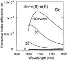
- Fig. 9 shows the refractive index change due to the application of the reverse electric field.
- FIG. 9 shows the wavelength-refractive index characteristics. In FIG. 9, it can be seen that as the applied electric field strength increases, the refractive index decreases, and the amount of decrease increases as the band gap is closer.
- the SiGe-PIN light modulation element of this embodiment can prevent the PIN structure from being formed in the SiGe semiconductor layer itself, and as a result, application of an electric field to the SiGe semiconductor layer can be reduced.
- a high concentration p-type Si semiconductor substrate doped with B (boron) is introduced into an UHV-CVD (Ultra High Vacuum Chemical Vapor Deposition) apparatus, and the substrate temperature is raised to 370 ° C.
- Ar-diluted GeH 4 gas (9%) is introduced at 70 sccm, the pressure in the growth chamber is set to 2.7 Pa, and an i-type Ge semiconductor buffer layer is grown by 30 nm on the p-type Si semiconductor layer in 60 minutes.
- the substrate temperature is raised to 600 ° C. and the flow rate of Ar-diluted GeH 4 gas (9%) and the pressure in the growth chamber are maintained. Grow until.
- B atoms doped in the Si semiconductor substrate diffuse into the i-type Ge semiconductor layer, so that the vicinity of the interface with the p-type Si semiconductor layer is p. Become a mold.
- a high-concentration p-type Si semiconductor substrate in which B (boron) is doped in an UHV-CVD (Ultra High Vacuum Chemical Vapor Deposition) apparatus First, a high-concentration p-type Si semiconductor substrate in which B (boron) is doped in an UHV-CVD (Ultra High Vacuum Chemical Vapor Deposition) apparatus. And the substrate temperature is raised to 370 ° C. Disilane (Si 2 H 6 ) gas and Ar diluted GeH 4 gas (9%) are introduced at 70 sccm, the pressure in the growth chamber is set to 2.7 Pa, and an i-type SiGe semiconductor buffer layer is formed on the p-type Si semiconductor layer in 60 minutes. Grow 30 nm.
- UHV-CVD Ultra High Vacuum Chemical Vapor Deposition
- the substrate temperature is increased to 600 ° C., and the i-type SiGe semiconductor layer is converted to the i-type in 100 minutes while maintaining the flow rate of disilane (Si 2 H 6 ) gas and Ar diluted GeH 4 gas (9%) and the pressure in the growth chamber.
- the SiGe semiconductor buffer layer is grown to 600 nm.
- B atoms doped in the Si semiconductor substrate diffuse into the i-type SiGe semiconductor layer, so that the vicinity of the interface with the p-type Si semiconductor layer is p. Become a mold.
- the Ar diluted GeH 4 gas (9%) or disilane (Si 2 H 6 ) gas and the Ar diluted GeH 4 gas (9%) were stopped, and the Si 2 H 6 gas (100%) was stopped.
- 3 sccm is introduced, the pressure in the growth chamber is 0.2 Pa, and the i-type Si semiconductor layer is grown by 200 nm on the i-type Ge semiconductor layer or the i-type SiGe semiconductor layer in 22 minutes.
- a 300 nm thick SiO 2 layer is formed on the i-type Si semiconductor layer by sputtering or the like.
- the SiO 2 layer is partially removed from the formed SiO 2 layer by photolithography.
- P is doped into the upper part of the i-type Si semiconductor layer where the SiO 2 layer is removed by ion implantation or the like.
- a heat treatment is performed at 650 ° C. for 30 minutes in an N 2 gas atmosphere to activate P in the i-type Si semiconductor layer. By activation, the upper part of the i-type Si semiconductor layer becomes n-type.
- An Al (aluminum) electrode is formed on the n-type Si semiconductor by vacuum deposition to complete an optical semiconductor element.
- the photoelectric conversion element or the light modulation element 30 as the optical semiconductor element of this embodiment includes an n-type Si semiconductor layer 31 and an i-type Si x Ge 1-x semiconductor layer by epitaxial growth. (However, 0 ⁇ x ⁇ 0.6) 21, an i-type Si semiconductor layer 22, and a p-type Si semiconductor layer 33 are sequentially stacked from the substrate to form a PIN structure.
- FIG. 10A shows that the photoelectric conversion element or the light modulation element 30 as the optical semiconductor element of this embodiment includes an n-type Si semiconductor layer 31 and an i-type Si x Ge 1-x semiconductor layer by epitaxial growth. (However, 0 ⁇ x ⁇ 0.6) 21, an i-type Si semiconductor layer 22, and a p-type Si semiconductor layer 33 are sequentially stacked from the substrate to form a PIN structure.
- FIG. 10A the photoelectric conversion element or the light modulation element 30 as the optical semiconductor element of this embodiment includes an n-type Si semiconductor layer 31 and an i-type
- the n-type Si semiconductor layer 31 is described as n-Si
- the i-type Si x Ge 1-x semiconductor layer 21 is described as i-Si x Ge 1-x
- the i-type Si semiconductor layer 22 Is described as i-Si
- the p-type Si semiconductor layer 33 is described as p-Si.
- the characteristic of the photoelectric conversion element or the light modulation element 30 is that it has a two-layer structure of a p-type Si semiconductor layer 33 and an i-type Si semiconductor layer 22 as shown in FIG.
- the thicknesses of the i-type Si x Ge 1-x semiconductor layer 21, the i-type Si semiconductor layer 22, the p-type Si semiconductor layer 33, and the n-type Si semiconductor layer 31 are the same as those in the first embodiment or the second embodiment.
- the i-type Si x Ge 1-x semiconductor layer 21, the i-type Si semiconductor layer 22, the n-type Si semiconductor layer 23, and the p-type Si semiconductor layer 11 have the same thickness.
- the photoelectric conversion element or the light modulation element 30 having the PIN structure may be formed only by epitaxial growth without performing high-temperature annealing at 700 to 900 ° C. as in the prior art. Epitaxial growth is usually performed at 650 ° C. or lower, and the temperature is not further raised during this process. Further, a doping material such as B (boron) is selected as the doping material for the p-type Si semiconductor layer 33, and P (phosphorus), As (arsenic), Sb (as the doping material for the n-type Si semiconductor layer 31). Antimony) or the like is selected.
- B boron
- P phosphorus
- As arsenic
- Sb as the doping material for the n-type Si semiconductor layer 31
- Antimony or the like is selected.
- the photoelectric conversion element or the light modulation element 30 may be manufactured without the high-temperature annealing treatment as described above, but as shown in FIG. 10B, the i-type Si x Ge 1-x semiconductor layer is formed in the epitaxial growth process.
- the i-type Si x Ge 1-x semiconductor layer 21 is formed in the epitaxial growth process.
- Si x Ge 1-x semiconductor layer 21b was described as Si x Ge 1-x semiconductor layer 21b.
- the i-type Si x Ge 1-x is affected by the doping material doped in the n-type Si semiconductor layer 31 and becomes n-type Si x Ge 1-x due to thermal diffusion.
- the i-type Si x Ge 1-x semiconductor layer 21 on the i-type Si semiconductor layer 22 side is not affected by the doping material because the i-type Si semiconductor layer 22 is intrinsic.
- this Ge-PIN photoelectric conversion element or light modulation element 30 can avoid the i-type Si x Ge 1-x semiconductor layer 21 from becoming the p-type on the i-type Si semiconductor layer 22 side. Therefore, it is possible to prevent the PIN structure from being formed in the i-type Si x Ge 1-x semiconductor layer 21.
- i-type Si x Ge 1-x semiconductor layer (where x 0) 21 and i-type Si semiconductor layer 22 and at least one i-type Si y Ge 1-y semiconductor layer (x ⁇ y It is desirable to further have ⁇ 1).
- the photoelectric conversion element or the light modulation element of the present embodiment includes an n-type Si semiconductor between the i-type Si x Ge 1-x semiconductor layer 21 and the i-type Si semiconductor layer 22. It is desirable to have any one of the semiconductor layer, the n-type Ge semiconductor layer, and the n-type SiGe semiconductor layer.
- the side near the i-type Si semiconductor layer 22 of the i - type Si x Ge 1-x semiconductor layer 21 is likely to be p-type.
- an electric field is applied to the SiGe semiconductor layer as in the conventional case, and dark current increases. Therefore, an n-type semiconductor layer 41 is added between the i-type Si x Ge 1-x semiconductor layer 21 and the i-type Si semiconductor layer 22 as in the photoelectric conversion element or the light modulation element 40 shown in FIG.
- An n-type Si semiconductor layer, an n-type Ge semiconductor layer, or an n-type SiGe semiconductor layer 41 disposed between the i-type Si x Ge 1-x semiconductor layer 21 and the i-type Si semiconductor layer 22 has an n-type carrier concentration. Is preferably 10 11 cm -2 or more and 10 14 cm -2 or less. It can be considered that there is no interface order because it is about 10 11 cm ⁇ 2 , and the same n-type carrier concentration is necessary to compensate the charge. Further, the n-type carrier concentration is about 10 14 cm ⁇ 2 as a limit value of doping.
- the photoelectric conversion element or the light modulation element of this embodiment may be an i-type Si p Ge 1-p semiconductor layer (0.5 ⁇ p ⁇ x) instead of the i-type Si semiconductor layer 22 in FIG. 10 or FIG. Good. From the viewpoint of reducing lattice mismatch with the p-type Si semiconductor layer 33, p ⁇ x is desirable. On the other hand, in order to suppress the generation of dark current due to application of an electric field, it is necessary to increase the band gap. From this viewpoint, 0.5 ⁇ p is desirable.
- the SiGe-PIN photoelectric conversion element or light modulation element of this embodiment can prevent the PIN structure from being formed in the SiGe semiconductor layer itself, and as a result, the application of an electric field to the SiGe semiconductor layer can be reduced. I was able to.
- n-type Si semiconductor substrate doped with As (arsenic) is introduced into a UHV-CVD (Ultra High Vacuum Chemical Vapor Deposition) apparatus, and the substrate temperature is raised to 370 ° C.
- Ar-diluted GeH 4 gas (9%) is introduced at 70 sccm, the pressure in the growth chamber is set to 2.7 Pa, and an i-type Ge semiconductor buffer layer is grown by 30 nm on the n-type Si semiconductor layer in 60 minutes.
- the substrate temperature is raised to 600 ° C. and the flow rate of Ar-diluted GeH 4 gas (9%) and the pressure in the growth chamber are maintained. Grow until.
- the i-type Ge semiconductor buffer layer and the i-type Ge semiconductor layer As atoms doped in the Si semiconductor substrate diffuse into the i-type Ge semiconductor layer, the vicinity of the interface with the n-type Si semiconductor layer is n. Become a mold.
- n-type Si x Ge 1-x semiconductor layer (x ⁇ 0)
- a high-concentration n-type Si semiconductor substrate doped with As (arsenic) in an UHV-CVD (Ultra High Vacuum Chemical Vapor Deposition) apparatus First, a high-concentration n-type Si semiconductor substrate doped with As (arsenic) in an UHV-CVD (Ultra High Vacuum Chemical Vapor Deposition) apparatus. And the substrate temperature is raised to 370 ° C. Disilane (Si 2 H 6 ) gas and Ar diluted GeH 4 gas (9%) are introduced at 70 sccm, the pressure in the growth chamber is set to 2.7 Pa, and an i-type SiGe semiconductor buffer layer is formed on the n-type Si semiconductor layer in 60 minutes. Grow 30 nm.
- Disilane (Si 2 H 6 ) gas and Ar diluted GeH 4 gas (9%) are introduced at 70 sccm
- the pressure in the growth chamber is set to
- the substrate temperature is increased to 600 ° C., and the i-type SiGe semiconductor layer is converted to the i-type in 100 minutes while maintaining the flow rate of disilane (Si 2 H 6 ) gas and Ar diluted GeH 4 gas (9%) and the pressure in the growth chamber.
- the SiGe semiconductor buffer layer is grown to 600 nm.
- the uppermost part of the i-type Ge semiconductor layer or the i-type SiGe semiconductor layer or the lowermost part of the i-type Si semiconductor layer to be grown next is doped with P (phosphorus) or As which becomes an n-type impurity.
- P phosphorus
- As which becomes an n-type impurity.
- a 300 nm thick SiO 2 layer is formed on the i-type Si semiconductor layer by sputtering or the like.
- the SiO 2 layer is partially removed from the formed SiO 2 layer by photolithography.
- B is doped on the upper part of the i-type Si semiconductor layer where the SiO 2 layer is removed by ion implantation or the like.
- a heat treatment is performed at 650 ° C. for 30 minutes in an N 2 gas atmosphere to activate B in the i-type Si semiconductor layer. By activation, the upper part of the i-type Si semiconductor layer becomes p-type.
- An Al (aluminum) electrode is formed on the p-type Si semiconductor by vacuum deposition to complete an optical semiconductor element.
- the Ge-PIN optical semiconductor element of the present invention is excellent in matching with a Si semiconductor integrated circuit based on a Si substrate, and can detect and modulate up to a long wavelength, so that it is integrated with a Si waveguide.
- the present invention can be applied to the obtained Si semiconductor integrated circuit.
Landscapes
- Light Receiving Elements (AREA)
- Optical Modulation, Optical Deflection, Nonlinear Optics, Optical Demodulation, Optical Logic Elements (AREA)
Abstract
本発明は、n型Si半導体層又はp型Si半導体層とi型SixGe1-x半導体層(但し、0≦x≦0.6)の間に、i型Si半導体層を配置することとした。つまり、p型Si半導体層、i型SixGe1-x半導体層(但し、0≦x≦0.6)、i型Si半導体層、n型Si半導体層が順に積層されたことを特徴とする光半導体素子、又はn型Si半導体層、i型SixGe1-x半導体層(但し、0≦x≦0.6)、i型Si半導体層、p型Si半導体層が順に積層されたことを特徴とする光半導体素子とした。
Description
本発明は、i型(真性型)SixGe1-x半導体を用いたPIN構造の光半導体素子に関し、特に、暗電流の少ない光半導体素子に関する。
Si(シリコン)半導体集積回路上で、長波長帯と呼ばれる1.6μm程度までの波長の光を検出するためには、Si半導体より禁制帯幅の狭いGe(ゲルマニウム)半導体を利用する必要がある。Si半導体集積回路上のGe-PIN光電変換素子としては、p型Si半導体層とn型Si半導体層との間にi型Ge半導体層を吸収層として形成したものがある。
従来の光電変換素子10の例を図1で説明する。図1(a)に一例を示すような従来の光電変換素子10は、エピタキシャル成長によって、図にはp-Siと記載したp型Si半導体層11と、i-Geと記載したi型Ge半導体層12と、n-Siと記載したn型Si半導体層13とが基板から順に積層され、PIN構造が形成されている。このPIN構造の光電変換素子10は上方から空間を介して光が照射されると光起電流を生ずる。また、光導波路を組み合わせる場合は、光電変換素子10は横方向又は下方向から光が照射され、光起電流を生ずる。
この種の光電変換素子として、特許文献1に記載の光起電力デバイスがある。この光起電力デバイスは、i型層を構成するアモルファスシリコンゲルマニウムにおけるGe原子の含有量を20乃至70原子%の範囲とし、Ge原子の含有量が積層方向において極大値をもつように分布させるとともに、p型層及びn型層と接する側にGe原子を含まない非単結晶シリコンバッファ層が設けられて構成されている。
一方、Si(シリコン)半導体集積回路上で、長波長帯と呼ばれる1.6μm程度までの波長の光を変調するためには、Si半導体より禁制帯幅の狭くかつ伝搬する光の波長よりも禁制帯幅の広いGe(ゲルマニウム)半導体を利用する必要がある。Si半導体集積回路上のGe-PIN光変調素子としては、p型Si半導体層とn型Si半導体層との間に外部電圧が0Vと特定の電圧Voとの間でi型Ge半導体層が伝搬光を透過あるいは吸収層として作用するように形成したものがある。これは電界吸収型の光変調素子と呼ばれている。
従来の光変調素子10の例を図1で説明する。図1(a)に一例を示すような従来の光変調素子10は、エピタキシャル成長によって、図にはp-Siと記載したp型Si半導体層11と、i-Geと記載したi型Ge半導体層12と、n-Siと記載したn型Si半導体層13とが基板から順に積層され、PIN構造が形成されている。このPIN構造の光変調素子10は、上方から空間を介して光が照射されると外部電圧が印加されている場合には光を吸収し、外部電圧が除去されると光を透過させる。また、光導波路を組み合わせる場合は、光変調素子10は横方向又は下方向から光が照射されると、外部電圧が印加されている場合には光を吸収し、外部電圧が除去されると光を透過させる。
この種の光変調素子として、非特許文献1に記載の光変調デバイスがある。この光変調デバイスは、i型層を構成するシリコンゲルマニウムにおけるGe原子の含有量を20乃至95原子%の範囲として構成されている。
"Waveguide-integrated ultralow-energy GeSi electro-absorption modulators" Jifeng Liu etal, Nature Photonics, online: 30 May, 2008
ところで、図1(a)に示した光電変換素子又は光変調素子10では、Ge半導体層を積層するとSi半導体層とGe半導体層と間で格子ミスマッチが発生する。この格子ミスマッチにより発生した格子欠陥が、暗電流の原因となる。格子欠陥を解消するため、700~900℃の高温アニール処理を実施する必要がある。しかし、Si半導体のエピタキシャル成長は通常650℃以下で行われる。Si半導体積層工程の途中で700~900℃になる高温アニール処理を施すことは好ましくない。
一方、暗電流の他の原因としては、次が挙げられる。i型Ge半導体層の両側界面が隣接するp型Si半導体層とn型Si半導体層によって、i型Ge半導体層の両側が、それぞれp型Ge半導体層とn型Ge半導体層になってしまい、Ge半導体層自身にPIN構造が形成されるという原因である。具体的には、図1(b)に示すように、p型Si半導体層11とi型Ge半導体層12との界面にp型Ge半導体層12aが生成されると共に、n型Si半導体層13とi型Ge半導体層12との界面にn型Ge半導体層12bが生成される。つまり、i型Ge半導体層12の中の両側にp型とn型が形成されるので、Ge半導体層自身がPIN構造となる。
即ち、Ge半導体層自身にPIN構造が形成されると、Ge半導体層に電界が印加されてしまう。Ge半導体は上記したように禁制帯幅が狭いため、電界の印加によって暗電流が生じやすい。
前記課題を解決するために、本発明は、p型Si半導体層とn型Si半導体層との間に光機能層を有する光半導体素子において、光機能層に印加される電界を低減することを目的とする。
さらに、前記課題を解決するために、本発明は、SiGe-PIN光半導体素子において、SiGe半導体層にPIN構造が形成されることを防止し、SiGe半導体層自身に印加される電界を低減することを目的とする。
上記目的を達成するために、本発明の光半導体素子は、p型Si半導体層とn型Si半導体層との間に光機能層及び電界制御層を挟むこととした。
具体的には、本発明の光半導体素子は、光機能層及び電界制御層を備える光半導体素子であり、p型Si半導体層とn型Si半導体層との間に前記光機能層及び前記電界制御層が挟まれていることを特徴とする光半導体素子とした。
この構成は、p型Si半導体層とn型Si半導体層との間に挟まれた光機能層で光半導体素子の機能を発揮させ、電界制御層で光機能層に電界が印加されないようにすることができる。
更に、具体的には、本発明の光半導体素子は、前記光機能層が、i型SixGe1-x半導体層(但し、0≦x≦0.6)を有することを特徴とする光半導体素子とした。
この構成は、Geが40%以上含まれることによって、長波長帯での使用を確保することができる。
更に、具体的には、前記電界制御層が、i型Si半導体層を有することを特徴とする光半導体素子とした。
この構成は、i型SixGe1-x半導体層とp型Si半導体層との間にi型Si半導体層が配置されるため、i型SixGe1-x半導体層のp型Si半導体層側に近い側がp型になることを避けることができる。あるいは、この構造は、i型SixGe1-x半導体層とn型Si半導体層との間にi型Si半導体層が配置されるため、i型SixGe1-x半導体層のn型Si半導体層側に近い側がn型になることを避けることができる。このため、この構造は、SixGe1-x半導体層自身にPIN構造が形成されることを防止することができる。すなわち、この構造は、SixGe1-x半導体層に電界が印加されないようにすることができる。
更に、具体的には、前記電界制御層が、前記光機能層と前記i型Si半導体層との間にn型Si半導体層、n型Ge半導体層及びn型SiGe半導体層のいずれかの半導体層をさらに有することを特徴とする光半導体素子とした。
i型SixGe1-x半導体層のi型Si半導体層に近い側はp型になり易い。i型SixGe1-x半導体層のi型Si半導体層に近い側がp型になると、従来と同じようにSiGe半導体層に電界が印加され、暗電流が増加するが、この構成は、前記i型SixGe1-x半導体層と前記i型Si半導体層との間にn型半導体層があることで、i型SixGe1-x半導体層のi型Si半導体層に近い側がp型になることを避けることができる。
また、上記目的を達成するために、本発明の光半導体素子は、i型SixGe1-x半導体層(但し、0≦x≦0.6)を反応領域とし、当該i型SixGe1-x半導体層とn型Si半導体層又はp型Si半導体層との間に、i型Si半導体層を配置することとした。
具体的には、本発明の光半導体素子は、p型Si半導体層、i型SixGe1-x半導体層(但し、0≦x≦0.6)、i型Si半導体層、n型Si半導体層が順に積層されたことを特徴とする光半導体素子とした。
この構成は、i型SixGe1-x半導体層とn型Si半導体層との間にi型Si半導体層が配置される。このため、この構造は、i型SixGe1-x半導体層のn型Si半導体層側に近い側がn型になることを避けることができ、Ge半導体層自身にPIN構造が形成されることを防止することができる。また、この構造は、i型SixGe1-x半導体層にGeが40%以上含まれることによって、長波長帯での使用を確保することができる。
更に、具体的には、本発明の光半導体素子は、n型Si半導体層、i型SixGe1-x半導体層(但し、0≦x≦0.6)、i型Si半導体層、p型Si半導体層が順に積層されたことを特徴とする光半導体素子とした。
この構成は、i型SixGe1-x半導体層とp型Si半導体層との間にi型Si半導体層が配置される。このため、この構造は、i型SixGe1-x半導体層のp型Si半導体層側に近い側がp型になることを避けることができ、SixGe1-x半導体層自身にPIN構造が形成されることを防止することができる。また、この構造は、i型SixGe1-x半導体層にGeが40%以上含まれることによって、長波長帯での使用を確保することができる。
本発明の光半導体素子は、上記光半導体素子において、前記i型SixGe1-x半導体層と前記i型Si半導体層との間に、n型Si半導体層、n型Ge半導体層及びn型SiGe半導体層のいずれかの半導体層を有することが望ましい。
i型SixGe1-x半導体層のi型Si半導体層に近い側はp型になり易い。i型SixGe1-x半導体層のi型Si半導体層に近い側がp型になると、従来と同じようにSiGe半導体層に電界が印加され、暗電流が増加するが、この構造は、前記i型SixGe1-x半導体層と前記i型Si半導体層との間にn型半導体層があることで、i型SixGe1-x半導体層のi型Si半導体層に近い側がp型になることを避けることができる。
本発明の光半導体素子は、上記光半導体素子において、前記i型SixGe1-x半導体層と前記i型Si半導体層との間に有する前記n型Si半導体層、前記n型Ge半導体層又は前記n型SiGe半導体層のn型キャリア濃度が1011cm-2以上、1014cm-2以下であることが望ましい。
界面準位がないとみなせるのは1011cm-2程度で、それを電荷補償するのに同程度のn型キャリア濃度が必要だからである。また、ドーピングの限界値としてn型キャリア濃度は1014cm-2程度である。
本発明の光半導体素子は、前述した光半導体素子において、前記i型Si半導体層の厚さが20nm以上であることが望ましい。
i型Si半導体層は0.3MeV/cmで破壊され、Ge半導体の禁制帯幅が0.6Vのため、0.6V÷0.3MeV/cm=20nm以上として破壊を防止することができる。
本発明の光半導体素子は、前述した光半導体素子において、前記i型SixGe1-x半導体層(但し、x=0)とその両側の層のうち少なくとも一方との間にi型SiyGe1-y半導体層(0<y<1)を更に有することが望ましい。
この構成は、i型SixGe1-x半導体層とn型Si半導体層又はp型Si半導体層との格子整合が容易である。
本発明の光電変換素子は、前述した光半導体素子に0V以上の逆バイアスを印加し、前記i型SixGe1-x半導体層に入射した光信号を電気信号に変換することを特徴とする光電変換素子である。
この構成は、0.8~1.6μmの波長の光信号を検出することができる。また、この構成は、暗電流が少ないため、SN比の高い光信号の検出が可能となる。
本発明の光変調素子は、前述した光半導体素子に印加する0V以上の逆バイアスを制御し、前記i型SixGe1-x半導体層に入射した光信号に対して吸収率を可変とすることを特徴とする光変調素子である。
この構成は、0.8~1.6μmの波長の光を変調することができる。また、この構成は、暗電流が少ないため、低消費電力で光を変調することができる。
本発明の光変調素子は、前述した光半導体素子に印加する0V以上の逆バイアスを制御し、前記i型SixGe1-x半導体層に入射した光信号に対して屈折率を可変とすることを特徴とする光変調素子。
この構成は、0.8~1.6μmの波長の光信号を変調することができる。また、この構成は、暗電流が少ないため、低消費電力で光を変調することができる。
本願において、光機能層とは光を電気に変換する光電変換機能、光を吸収する割合を可変する吸収率可変機能、光に対する屈折率を可変する屈折率可変機能のいずれかを有する層をいう。
本願において、電界制御層とは光機能層とn型Si半導体層又はp型Si半導体層との間にあって、光機能層に印加される電界を低減する機能を有する層をいう。
本願において、i型半導体とは不純物がドーピングされていない真性半導体をいう。n型半導体とは、電子をキャリアとする半導体をいい、p型半導体とは正孔をキャリアとする半導体をいう。
本発明によれば、p型Si半導体層とn型Si半導体層との間に光機能層を有する光半導体素子において、光機能層に印加される電界を低減することができる。
さらに、本発明によれば、SiGe-PIN光半導体素子において、SiGe半導体層にPIN構造が形成されることを防止して、SiGe半導体層自身に印加される電界を低減することができる。
添付の図面を参照して本発明の実施形態を説明する。以下に説明する実施形態は本発明の実施例であり、本発明は、以下の実施形態に制限されるものではない。なお、本明細書及び図面において符号が同じ構成要素は、相互に同一のものを示すものとする。
(第1の実施形態)
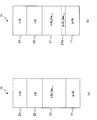
本発明の第1の実施形態に係る光電変換素子の構成を図2で説明する。本実施形態の光半導体素子としての光電変換素子20は、図2(a)に示すように、エピタキシャル成長によって、p型Si半導体層11と、i型SixGe1-x半導体層(但し、0≦x≦0.6)21と、i型Si半導体層22と、n型Si半導体層23とが基板から順に積層され、PIN構造が形成されている。但し、図2では、p型Si半導体層11はp-Siと記載し、i型SixGe1-x半導体層21はi-SixGe1-xと記載し、i型Si半導体層22はi-Siと記載し、n型Si半導体層23はn-Siと記載した。
本発明の第1の実施形態に係る光電変換素子の構成を図2で説明する。本実施形態の光半導体素子としての光電変換素子20は、図2(a)に示すように、エピタキシャル成長によって、p型Si半導体層11と、i型SixGe1-x半導体層(但し、0≦x≦0.6)21と、i型Si半導体層22と、n型Si半導体層23とが基板から順に積層され、PIN構造が形成されている。但し、図2では、p型Si半導体層11はp-Siと記載し、i型SixGe1-x半導体層21はi-SixGe1-xと記載し、i型Si半導体層22はi-Siと記載し、n型Si半導体層23はn-Siと記載した。
光電変換素子20の特徴は、図1(a)に示したGe-PIN構造において、上部層のn型Si半導体層13を、図2に示すように、n型Si半導体層23及びi型Si半導体層22の2層構造とした点にある。
i型SixGe1-x半導体層21の厚さは、例えば、500nm~30μmである。i型SixGe1-x半導体層21は厚さが500nm以上であれば有効に光子を捕捉することができる。一方、i型SixGe1-x半導体層21に空乏層が形成される限界の厚さは30μm程度である。i型Si半導体層22の厚さは、例えば、20nm~10μmである。i型Si半導体は0.3MeV/cmで破壊され、Ge半導体の禁制帯幅は0.6Vのため、0.6V÷0.3MeV/cm=20nm以上として破壊を防止することができる。i型Si半導体層22は厚さが10μm程度までであれば、エピタキシャル成長でi型Si半導体の結晶性の均一性を十分に維持できる。n型Si半導体層23の厚さは、100nm程度である。この厚さは、エピタキシャル成長で形成でき、電極として十分な厚さである。p型Si半導体層11の厚さは電極として機能できる厚さであればよい。例えば、Si基板の上面にp型Si半導体層11を積層してもよいし、Si半導体基板をドーピングによりp型化してp型Si半導体層11を形成してもよい。
i型Si半導体層22及びi型SixGe1-x半導体層21は、高速光信号の検出用にはキャリア走行時間を短くするために薄く、低速光信号の検出では光子を効率的に捕捉するために厚く積層される。
更に、このPIN構造の光電変換素子20は、従来のように700~900℃の高温アニール処理は行わず、エピタキシャル成長のみで形成してもよい。エピタキシャル成長は通常、650℃以下で行い、この途中で更に温度を上昇させないようにする。また、p型Si半導体層11のドーピング材料には、B(ボロン)等のドーピング材料が選択され、n型Si半導体層23のドーピング材料には、P(リン)、As(ヒ素)、Sb(アンチモン)等が選択される。
光電変換素子20の製造は、上述したように高温アニール処理を不要としてもよいが、図2(b)に示すように、エピタキシャル成長工程で、i型SixGe1-x半導体層21のp型Si半導体層11の側に、p-SixGe1-xと記載したp型SixGe1-x半導体層21aを形成する。これは、熱拡散によって、i型SixGe1-xがp型Si半導体層11にドーピングされたドーピング材料に影響されてp型SixGe1-xとなるからである。一方、i型SixGe1-x半導体層21のi型Si半導体層22の側は、i型Si半導体層22が真性型であるためドーピング材料による影響はない。
以上説明したように、この光電変換素子は、i型SixGe1-x半導体層21のi型Si半導体層22の側がn型となることを避けることができ、i型SixGe1-x半導体層21にPIN構造が形成されることを防止できる。
なお、本実施形態の光電変換素子は、i型SixGe1-x半導体層21において、x=0としたとき、i型SixGe1-x半導体層(但し、x=0)21とp型Si半導体層11との間(図2(b)においては、p型SixGe1-x半導体層(但し、x=0)21aとp型Si半導体層11との間)、又はi型SixGe1-x半導体層(但し、x=0)21とi型Si半導体層22との間のうち少なくとも一方にi型SiyGe1-y半導体層(x<y<1)を更に有することが望ましい。このような構成とすれば、i型SixGe1-x半導体層(但し、x=0)21とp型Si半導体層11との間(図2(b)においては、p型SixGe1-x半導体層(但し、x=0)21aとp型Si半導体層11との間)、又はi型SixGe1-x半導体層(但し、x=0)21とi型Si半導体層22との間の格子整合が容易となる。
本実施形態の光電変換素子は、図2におけるi型Si半導体層22に替えて、i型SipGe1-p半導体層(0.5<p<x)としてもよい。n型Si半導体層23との格子ミスマッチを小さくする観点から、p<xが望ましい。一方、電界印加による暗電流の発生を抑圧するためには、バンドギャップを大きくする必要があり、この観点からは0.5<pが望ましい。
次に、n型Si半導体層とi型SixGe1-x半導体層(但し、0≦x≦0.6)の間に、i型Si半導体層を配置することによる効果を確認する。図3は、Ge-PINの積層方向に対して印加される外部バイアスによる禁制帯幅の変化を計算によって求めた結果である。但し、x=0で計算している。図3(a)は、p型Si半導体層、i型SixGe1-x半導体層、n型Si半導体層が順に積層されたモデルであり、図3(b)は、p型Si半導体層、i型SixGe1-x半導体層、i型Si半導体層、n型Si半導体層が順に積層されたモデルである。
i型Si半導体層のない図3(a)では、外部バイアス電圧が0Vのときでも、i型SixGe1-x半導体層に電位差が生じ、外部バイアス電圧が3Vになると、i型SixGe1-x半導体層に大きな電位差が生じている。一方、i型Si半導体層のある図3(b)では、外部バイアス電圧が0Vのときには、i型SixGe1-x半導体層に電位差がほとんど生じず、外部バイアス電圧が3Vになっても、i型SixGe1-x半導体層には小さい電位差しか生じていない。このことから、n型Si半導体層とi型SixGe1-x半導体層(但し、0≦x≦0.6)の間に、i型Si半導体層を配置することによって、SixGe1-x半導体層にPIN構造が形成されないことが分かる。
SixGe1-x半導体層にPIN構造が形成されないことによって、暗電流を抑圧できることを確認した。図4は、Ge-PINに印加される外部バイアスによる暗電流の変化を実験によって求めた結果である。但し、x=0で実験した。図4(a)は、p型Si半導体層、i型SixGe1-x半導体層、n型Si半導体層が順に積層された光電変換素子(図中の実線)及びp型Si半導体層、i型SixGe1-x半導体層、i型Si半導体層、n型Si半導体層が順に積層された光電変換素子(図中の破線)をアニール処理した結果である。図4(b)は、p型Si半導体層、i型SixGe1-x半導体層、n型Si半導体層が順に積層された光電変換素子(図中の実線)及びp型Si半導体層、i型SixGe1-x半導体層、i型Si半導体層、n型Si半導体層が順に積層された光電変換素子(図中の破線)をアニール処理しなかった結果である。
アニール処理をしない図4(b)では、i型Si半導体層のない場合は外部バイアスの印加によって、暗電流が大きく増大しているが、i型Si半導体層のある場合は暗電流の増大を大きく抑圧できていることが分かる。一方、アニール処理をした図4(a)では、i型Si半導体層のある場合もない場合も暗電流の増大を大きく抑圧できており、i型Si半導体層のある場合はさらに暗電流の増大を抑圧できることが分かる。
i型Si半導体層を配置しても感度が劣化しないことを実験によって確認した。図5は、Ge-PINに印加される外部バイアスをパラメータとする波長-感度特性である。図5(a)は、p型Si半導体層、i型SixGe1-x半導体層、n型Si半導体層が順に積層された光電変換素子をアニール処理した結果であり、図5(b)は、p型Si半導体層、i型SixGe1-x半導体層、i型Si半導体層、n型Si半導体層が順に積層された光電変換素子をアニール処理しなかった結果である。
図5(a)と図5(b)では、バイアスを印加すると波長-感度特性に大きな差はなく、p型Si半導体層、i型SixGe1-x半導体層、i型Si半導体層、n型Si半導体層が順に積層された光電変換素子でも十分な感度を実現できることが分かる。
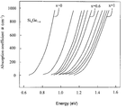
i型SixGe1-x半導体層における混晶比について説明する。図6はxをパラメータとするエネルギーに対する吸収係数αの関係を示すものである。波長0.85μm以上の光を検出することを想定すると、波長0.85μmはエネルギーとして1.45eVである。このとき、吸収係数αが1000cm-1以上の条件では、x≦0.6となる。つまり、波長0.85μm以上の波長を検出するためには、i型SixGe1-x半導体層におけるSiの比率を0.6以下とすればよいことが分かる。
本実施形態のSiGe-PIN光電変換素子は、SiGe半導体層自身にPIN構造が形成されることを防止することができ、この結果、SiGe半導体層への電界の印加を低減することができた。
(第2の実施形態)
本発明の第2の実施形態に係る光変調素子の構成を図2で説明する。本実施形態の光半導体素子としての光変調素子20は、図2(a)に示すように、エピタキシャル成長によって、p型Si半導体層11と、i型SixGe1-x半導体層(但し、0≦x≦0.6)21と、i型Si半導体層22と、n型Si半導体層23とが基板から順に積層され、PIN構造が形成されている。但し、図2では、p型Si半導体層11はp-Siと記載し、i型SixGe1-x半導体層21はi-SixGe1-xと記載し、i型Si半導体層22はi-Siと記載し、n型Si半導体層23はn-Siと記載した。
本発明の第2の実施形態に係る光変調素子の構成を図2で説明する。本実施形態の光半導体素子としての光変調素子20は、図2(a)に示すように、エピタキシャル成長によって、p型Si半導体層11と、i型SixGe1-x半導体層(但し、0≦x≦0.6)21と、i型Si半導体層22と、n型Si半導体層23とが基板から順に積層され、PIN構造が形成されている。但し、図2では、p型Si半導体層11はp-Siと記載し、i型SixGe1-x半導体層21はi-SixGe1-xと記載し、i型Si半導体層22はi-Siと記載し、n型Si半導体層23はn-Siと記載した。
光変調素子20の特徴は、図1(a)に示したGe-PIN構造において、上部層のn型Si半導体層13を、図2に示すように、n型Si半導体層23及びi型Si半導体層22の2層構造とした点にある。
i型SixGe1-x半導体層21の厚さは、例えば、200nm~10μmである。i型SixGe1-x半導体層21は厚さが200nm以上であればこの層を伝搬する光のモードを単一モードとすることができ、変調素子を通過した光子を引き続く光導波路内を単一モードで伝搬させることができる。上記はチャネル導波路の場合である。一方、リブ導波路の場合、i型SixGe1-x半導体層21は単一モードが伝搬できる厚さまで厚くすることができる。リブ導波路の単一モードが形成される限界の厚さは10μm程度である。i型Si半導体層22の厚さは、例えば、20nm~10μmである。i型Si半導体は0.3MeV/cmで破壊され、Ge半導体の禁制帯幅は0.6Vのため、i型Si半導体層22の厚さは、0.6V÷0.3MeV/cm=20nm以上として破壊を防止することができる。i型Si半導体層22は厚さが10μm程度までであれば、エピタキシャル成長でi型Si半導体の結晶性の均一性を十分に維持できる。n型Si半導体層23の厚さは、100nm程度である。この厚さは、エピタキシャル成長で形成でき、電極として十分な厚さである。p型Si半導体層11の厚さは電極として機能できる厚さであればよい。例えば、Si基板の上面にp型Si半導体層11を積層してもよいし、Si半導体基板をドーピングによりp型化してp型Si半導体層11を形成してもよい。
i型Si半導体層22及びi型SixGe1-x半導体層21は、高速光信号の変調用には抵抗・容量積(充放電時間)を短くするために薄く積層される。但し、i型Si半導体層22及びi型SixGe1-x半導体層21は、単一モードを満たす厚さ(チャネル導波路では100nm程度)が必要である。
更に、このPIN構造の光変調素子20は、従来のように700~900℃の高温アニール処理は行わず、エピタキシャル成長のみで形成してもよい。エピタキシャル成長は通常、650℃以下で行い、この途中で更に温度を上昇させないようにする。また、p型Si半導体層11のドーピング材料には、B(ボロン)等のドーピング材料が選択され、n型Si半導体層23のドーピング材料には、P(リン)、As(ヒ素)、Sb(アンチモン)等が選択される。
光変調素子20の製造は、上述したように高温アニール処理を不要としてもよいが、図2(b)に示すように、エピタキシャル成長工程で、i型SixGe1-x半導体層21のp型Si半導体層11の側に、p-SixGe1-xと記載したp型SixGe1-x半導体層21aを形成する。これは、熱拡散によって、i型SixGe1-xがp型Si半導体層11にドーピングされたドーピング材料に影響されてp型SixGe1-xとなるからである。一方、i型SixGe1-x半導体層21のi型Si半導体層22の側は、i型Si半導体層22が真性型であるためドーピング材料による影響はない。
以上説明したように、この光変調素子は、i型SixGe1-x半導体層21のi型Si半導体層22の側がn型となることを避けることができ、i型SixGe1-x半導体層21にPIN構造が形成されることを防止できる。
なお、本実施形態の光変調素子は、i型SixGe1-x半導体層21において、x=0としたとき、i型SixGe1-x半導体層(但し、x=0)21とp型Si半導体層11との間(図2(b)においては、p型SixGe1-x半導体層(但し、x=0)21aとp型Si半導体層11との間)、又はi型SixGe1-x半導体層(但し、x=0)21とi型Si半導体層22との間のうち少なくとも一方にi型SiyGe1-y半導体層(x<y<1)を更に有することが望ましい。このような構成とすれば、i型SixGe1-x半導体層(但し、x=0)21とp型Si半導体層11との間(図2(b)においては、p型SixGe1-x半導体層(但し、x=0)21aとp型Si半導体層11との間)、又はi型SixGe1-x半導体層(但し、x=0)21とi型Si半導体層22との間の格子整合が容易となる。
本実施形態の光変調素子は、図2におけるi型Si半導体層22に替えて、i型SipGe1-p半導体層(0.5<p<x)としてもよい。n型Si半導体層23との格子ミスマッチを小さくする観点から、p<xが望ましい。一方、電界印加による暗電流の発生を抑圧するためには、バンドギャップを大きくする必要があり、この観点からは0.5<pが望ましい。
次に、n型Si半導体層とi型SixGe1-x半導体層(但し、0≦x≦0.6)の間に、i型Si半導体層を配置することによる効果を確認する。図3は、Ge-PINの積層方向に対して印加される外部バイアスによる禁制帯幅の変化を計算によって求めた結果である。但し、x=0で計算している。図3(a)は、p型Si半導体層、i型SixGe1-x半導体層、n型Si半導体層が順に積層されたモデルであり、図3(b)は、p型Si半導体層、i型SixGe1-x半導体層、i型Si半導体層、n型Si半導体層が順に積層されたモデルである。
i型Si半導体層のない図3(a)では、外部バイアス電圧が0Vのときでも、i型SixGe1-x半導体層に電位差が生じ、これは、20kV/cmに相当する。外部バイアス電圧が3Vになると、i型SixGe1-x半導体層に大きな電位差が生じている。一方、i型Si半導体層のある図3(b)では、外部バイアス電圧が0Vのときには、i型SixGe1-x半導体層に電位差がほとんど生じず、外部バイアス電圧が3Vになっても、i型SixGe1-x半導体層には小さい電位差しか生じていない。このことから、n型Si半導体層とi型SixGe1-x半導体層(但し、0≦x≦0.6)の間に、i型Si半導体層を配置することによって、SixGe1-x半導体層にPIN構造が形成されないことが分かる。また、同じ電界を印加しても、i型Si半導体層のない光変調素子よりもi型Si半導体層のある場合光変調素子の方が、強いFK(Franz-Keldysh)効果が得られることが分かる。なお、FK効果とは、半導体に直流電場を印加すると、伝導帯と価電子帯のエネルギーバンドが傾き、電子と正孔の波動関数がエネルギーギャップ内に浸み出し、そのため実効的なエネルギーギャップが無電界時のエネルギーギャップEgより小さくなる効果をいう。
SixGe1-x半導体層にPIN構造が形成されないことによって、暗電流を抑圧できることを確認した。図4は、Ge-PINに印加される外部バイアスによる暗電流の変化を実験によって求めた結果である。但し、x=0で実験した。図4(a)は、p型Si半導体層、i型SixGe1-x半導体層、n型Si半導体層が順に積層された光変調素子(図中の実線)及びp型Si半導体層、i型SixGe1-x半導体層、i型Si半導体層、n型Si半導体層が順に積層された光変調素子(図中の破線)をアニール処理した結果であり、図4(b)は、p型Si半導体層、i型SixGe1-x半導体層、n型Si半導体層が順に積層された光変調素子(図中の実線)及びp型Si半導体層、i型SixGe1-x半導体層、i型Si半導体層、n型Si半導体層が順に積層された光変調素子(図中の破線)をアニール処理しなかった結果である。
アニール処理をしない図4(b)では、i型Si半導体層のない場合は外部バイアスの印加によって、暗電流が大きく増大しているが、i型Si半導体層のある場合は暗電流の増大を大きく抑圧できていることが分かる。一方、アニール処理をした図4(a)では、i型Si半導体層のある場合もない場合も暗電流の増大を大きく抑圧できており、i型Si半導体層のある場合はさらに暗電流の増大を抑圧できることが分かる。
i型SixGe1-x半導体層における混晶比について説明する。図6はxをパラメータとするエネルギーに対する吸収係数αの関係を示すものである。波長0.85μm以上の光を変調することを想定すると、波長0.85μmはエネルギーとして1.45eVである。このとき、吸収係数αが1000cm-1以上の条件では、x≦0.6となる。つまり、波長0.85μm以上の波長を変調するためには、i型SixGe1-x半導体層はSiの比率を0.6とすればよい。さらに、図に示すように、電界強度が増大することにより、光の吸収が増大するため、電界吸収型の光変調素子をつくることができる。
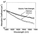
i型Si半導体層を配置した光変調素子の波長-吸収特性を実験によって確認した。図7は、Ge-PINに印加される外部バイアスをパラメータとする波長-吸収特性である。図7のように、バイアスの大きさを制御することにより吸収特性が大きく変化する。このため、p型Si半導体層、i型SixGe1-x半導体層、i型Si半導体層、n型Si半導体層が順に積層された光変調素子は、十分な変調を実現できることが分かる。
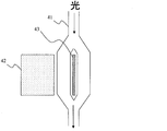
本実施形態の光変調素子は、i型SixGe1-x半導体層を吸収又は透過させて光信号を変調するだけでなく、屈折率変化を利用して光信号を変調することもできる。マッハ・ツェンダ型変調器の構成を図8に示す。図8において、図上の上側から導波路41に入力された光は、左右の導波路に2分岐される。p電極42とn電極43との間に逆方向電界が印加された時に、FK効果により導波路の屈折率は低下する。このため、図上の左側の導波路を伝搬した光の位相は、ずれることになる。左右の導波路に2分岐された光が合流するとき、両者の位相がπだけずれていると、図上の下側の導波路からは光が出なくなる。このように、本実施形態の光変調素子は、一方の光路に印加する逆方向電界を制御することにより、光の強度変調が可能になる。
逆方向電界の印加による屈折率変化を図9に示す。図9は波長-屈折率特性である。図9において、印加電界強度が高まるにつれて、屈折率は低下し、その低下量は、バンドギャップに近いほど大きくなることが分かる。
本実施形態のSiGe-PIN光変調素子は、SiGe半導体層自身にPIN構造が形成されることを防止することができ、この結果、SiGe半導体層への電界の印加を低減することができた。
(第3の実施形態)
次に、p型Si半導体層、i型SixGe1-x半導体層、i型Si半導体層、n型Si半導体層が順に積層された光半導体素子の製造工程について説明する。但し、本製造工程では、断らない限りx=0の場合について説明する。
次に、p型Si半導体層、i型SixGe1-x半導体層、i型Si半導体層、n型Si半導体層が順に積層された光半導体素子の製造工程について説明する。但し、本製造工程では、断らない限りx=0の場合について説明する。
まず、UHV-CVD(Ultra High Vacuum Chemical Vapor Deposition)装置にB(ボロン)をドーピングした高濃度p型Si半導体基板を導入し、基板温度を370℃に上昇させる。Ar希釈GeH4ガス(9%)を70sccm導入し、成長室内の圧力を2.7Paとして、60分間でp型Si半導体層上にi型Ge半導体緩衝層を30nmだけ成長させる。
基板温度を600℃まで上昇させ、Ar希釈GeH4ガス(9%)の流量と成長室内の圧力を維持したまま、100分間でi型Ge半導体層をi型Ge半導体緩衝層と合わせて600nmとなるまで成長させる。i型Ge半導体緩衝層及びi型Ge半導体層を成長中に、Si半導体基板にドープされているB原子がi型Ge半導体層に拡散することにより、p型Si半導体層との界面付近はp型となる。
i型SixGe1-x半導体層(x≠0)を成長させる場合は、まず、UHV-CVD(Ultra High Vacuum Chemical Vapor Deposition)装置にB(ボロン)をドーピングした高濃度p型Si半導体基板を導入し、基板温度を370℃に上昇させる。ジシラン(Si2H6)ガスとAr希釈GeH4ガス(9%)を70sccm導入し、成長室内の圧力を2.7Paとして、60分間でp型Si半導体層上にi型SiGe半導体緩衝層を30nmだけ成長させる。基板温度を600℃まで上昇させ、ジシラン(Si2H6)ガスとAr希釈GeH4ガス(9%)の流量と成長室内の圧力を維持したまま、100分間でi型SiGe半導体層をi型SiGe半導体緩衝層と合わせて600nmとなるまで成長させる。i型SiGe半導体緩衝層及びi型SiGe半導体層を成長中に、Si半導体基板にドープされているB原子がi型SiGe半導体層に拡散することにより、p型Si半導体層との界面付近はp型となる。
次に、基板温度を維持したまま、Ar希釈GeH4ガス(9%)又はジシラン(Si2H6)ガスとAr希釈GeH4ガス(9%)を止め、Si2H6ガス(100%)を3sccm導入し、成長室内の圧力を0.2Paとして、22分間でi型Ge半導体層上又はi型SiGe半導体層上にi型Si半導体層を200nmだけ成長させる。
試料を成長室から取り出した後、スパッタリング法等により、i型Si半導体層上に300nm厚のSiO2層を形成する。形成したSiO2層からフォトリソグラフィにより部分的にSiO2層を除去する。イオン注入法などによりSiO2層を除去した部分のi型Si半導体層の上部にPをドーピングする。N2ガス雰囲気中で650℃、30分間熱処理し、i型Si半導体層中のPを活性化する。活性化により、i型Si半導体層の上部がn型化する。n型Si半導体上に真空蒸着法によりAl(アルミニウム)電極を形成して、光半導体素子が完成する。
(第4の実施形態)
本発明の第4の実施形態に係る光半導体素子の構成を図10で説明する。本実施形態の光半導体素子としての光電変換素子あるいは光変調素子30は、図10(a)に示すように、エピタキシャル成長によって、n型Si半導体層31と、i型SixGe1-x半導体層(但し、0≦x≦0.6)21と、i型Si半導体層22と、p型Si半導体層33とが基板から順に積層され、PIN構造が形成されている。但し、図10では、n型Si半導体層31はn-Siと記載し、i型SixGe1-x半導体層21はi-SixGe1-xと記載し、i型Si半導体層22はi-Siと記載し、p型Si半導体層33はp-Siと記載した。
本発明の第4の実施形態に係る光半導体素子の構成を図10で説明する。本実施形態の光半導体素子としての光電変換素子あるいは光変調素子30は、図10(a)に示すように、エピタキシャル成長によって、n型Si半導体層31と、i型SixGe1-x半導体層(但し、0≦x≦0.6)21と、i型Si半導体層22と、p型Si半導体層33とが基板から順に積層され、PIN構造が形成されている。但し、図10では、n型Si半導体層31はn-Siと記載し、i型SixGe1-x半導体層21はi-SixGe1-xと記載し、i型Si半導体層22はi-Siと記載し、p型Si半導体層33はp-Siと記載した。
光電変換素子あるいは光変調素子30の特徴は、図10に示すように、p型Si半導体層33及びi型Si半導体層22の2層構造とした点にある。
i型SixGe1-x半導体層21、i型Si半導体層22、p型Si半導体層33及びn型Si半導体層31のそれぞれの厚さは、第1の実施形態又は第2の実施形態におけるi型SixGe1-x半導体層21、i型Si半導体層22、n型Si半導体層23、p型Si半導体層11のそれぞれの厚さと同様である。
更に、このPIN構造の光電変換素子あるいは光変調素子30は、従来のように700~900℃の高温アニール処理は行わず、エピタキシャル成長のみで形成してもよい。エピタキシャル成長は通常、650℃以下で行い、この途中で更に温度を上昇させないようにする。また、p型Si半導体層33のドーピング材料には、B(ボロン)等のドーピング材料が選択され、n型Si半導体層31のドーピング材料には、P(リン)、As(ヒ素)、Sb(アンチモン)等が選択される。
光電変換素子あるいは光変調素子30の製造は、上述したように高温アニール処理を不要としてもよいが、図10(b)に示すように、エピタキシャル成長工程で、i型SixGe1-x半導体層21のn型Si半導体層31の側に、n-SixGe1-xと記載したn型SixGe1-x半導体層21bを形成する。これは、熱拡散によって、i型SixGe1-xがn型Si半導体層31にドーピングされたドーピング材料に影響されてn型SixGe1-xとなるからである。一方、i型SixGe1-x半導体層21のi型Si半導体層22の側は、i型Si半導体層22が真性型であるためドーピング材料による影響はない。
以上説明したように、このGe-PIN光電変換素子あるいは光変調素子30は、i型SixGe1-x半導体層21のi型Si半導体層22の側がp型となることを避けることができ、i型SixGe1-x半導体層21にPIN構造が形成されることを防止できる。
なお、本実施形態の光電変換素子あるいは光変調素子では、i型SixGe1-x半導体層21において、x=0としたとき、i型SixGe1-x半導体層(但し、x=0)21とn型Si半導体層31との間(図10(b)においては、n型SixGe1-x半導体層(但し、x=0)21bとn型Si半導体層31との間)、又はi型SixGe1-x半導体層(但し、x=0)21とi型Si半導体層22との間のうち少なくとも一方にi型SiyGe1-y半導体層(x<y<1)を更に有することが望ましい。このような構成とすれば、i型SixGe1-x半導体層(但し、x=0)21とn型Si半導体層31との間(図10(b)においては、n型SixGe1-x半導体層(但し、x=0)21bとn型Si半導体層31との間)、又はi型SixGe1-x半導体層(但し、x=0)21とi型Si半導体層22との間の格子整合が容易となる。
ここで、本実施形態の光電変換素子あるいは光変調素子は、図11に示すように、i型SixGe1-x半導体層21とi型Si半導体層22との間に、n型Si半導体層、n型Ge半導体層及びn型SiGe半導体層のいずれかの半導体層を有することが望ましい。
図10に示す光電変換素子あるいは光変調素子30の構成は、i型SixGe1-x半導体層21のi型Si半導体層22に近い側がp型になり易い。i型SixGe1-x半導体層21のi型Si半導体層22に近い側がp型になると、従来と同じようにSiGe半導体層に電界が印加され、暗電流が増加する。そこで、図11に示す光電変換素子あるいは光変調素子40のように、i型SixGe1-x半導体層21とi型Si半導体層22との間にn型半導体層41を追加することにより、i型SixGe1-x半導体層21のi型Si半導体層22に近い側がp型になることを確実に避けることができる。これにより、i型SixGe1-x半導体層にPIN構造が形成されることを防止できる。
i型SixGe1-x半導体層21とi型Si半導体層22との間に配置される、n型Si半導体層、n型Ge半導体層又はn型SiGe半導体層41は、n型キャリア濃度が1011cm-2以上、1014cm-2以下であることが望ましい。界面順位がないとみなせるのは1011cm-2程度で、それを電荷補償するのに同程度のn型キャリア濃度が必要だからである。また、ドーピングの限界値としてn型キャリア濃度は1014cm-2程度である。
本実施形態の光電変換素子あるいは光変調素子は、図10又は図11におけるi型Si半導体層22に替えて、i型SipGe1-p半導体層(0.5<p<x)としてもよい。p型Si半導体層33との格子ミスマッチを小さくする観点から、p<xが望ましい。一方、電界印加による暗電流の発生を抑圧するためには、バンドギャップを大きくする必要があり、この観点からは0.5<pが望ましい。
本実施形態のSiGe-PIN光電変換素子あるいは光変調素子は、SiGe半導体層自身にPIN構造が形成されることを防止することができ、この結果、SiGe半導体層への電界の印加を低減することができた。
(第5の実施形態)
次に、n型Si半導体層、i型SixGe1-x半導体層、n型Ge半導体層、i型Si半導体層、p型Si半導体層が順に積層された光半導体素子としての光電変換素子あるいは光変調素子の製造工程について説明する。但し、本製造工程では、断らない限りx=0の場合について説明する。
次に、n型Si半導体層、i型SixGe1-x半導体層、n型Ge半導体層、i型Si半導体層、p型Si半導体層が順に積層された光半導体素子としての光電変換素子あるいは光変調素子の製造工程について説明する。但し、本製造工程では、断らない限りx=0の場合について説明する。
まず、UHV-CVD(Ultra High Vacuum Chemical Vapor Deposition)装置にAs(砒素)をドーピングした高濃度n型Si半導体基板を導入し、基板温度を370℃に上昇させる。Ar希釈GeH4ガス(9%)を70sccm導入し、成長室内の圧力を2.7Paとして、60分間でn型Si半導体層上にi型Ge半導体緩衝層を30nmだけ成長させる。
基板温度を600℃まで上昇させ、Ar希釈GeH4ガス(9%)の流量と成長室内の圧力を維持したまま、100分間でi型Ge半導体層をi型Ge半導体緩衝層と合わせて600nmとなるまで成長させる。i型Ge半導体緩衝層及びi型Ge半導体層を成長中に、Si半導体基板にドープされているAs原子がi型Ge半導体層に拡散することにより、n型Si半導体層との界面付近はn型となる。
i型SixGe1-x半導体層(x≠0)を成長させる場合は、まず、UHV-CVD(Ultra High Vacuum Chemical Vapor Deposition)装置にAs(砒素)をドーピングした高濃度n型Si半導体基板を導入し、基板温度を370℃に上昇させる。ジシラン(Si2H6)ガスとAr希釈GeH4ガス(9%)を70sccm導入し、成長室内の圧力を2.7Paとして、60分間でn型Si半導体層上にi型SiGe半導体緩衝層を30nmだけ成長させる。基板温度を600℃まで上昇させ、ジシラン(Si2H6)ガスとAr希釈GeH4ガス(9%)の流量と成長室内の圧力を維持したまま、100分間でi型SiGe半導体層をi型SiGe半導体緩衝層と合わせて600nmとなるまで成長させる。i型SiGe半導体緩衝層及びi型SiGe半導体層を成長中に、Si半導体基板にドープされているAs原子がi型SiGe半導体層に拡散することにより、n型Si半導体層との界面付近はn型となる。
次に、i型Ge半導体層又はi型SiGe半導体層の最上部又は次に成長させるi型Si半導体層の最下部にn型不純物となるP(リン)あるいはAsをドーピングする。これにより、i型Ge半導体層又はi型SiGe半導体層の最上部はn型となる。i型Si半導体層の最下部にn型不純物をドーピングしても、熱拡散により、i型Ge半導体層又はi型SiGe半導体層の最上部はn型となる。
基板温度を維持したまま、Ar希釈GeH4ガス(9%)又はジシラン(Si2H6)ガスとAr希釈GeH4ガス(9%)を止め、Si2H6ガス(100%)を3sccm導入し、成長室内の圧力を0.2Paとして、22分間でn型Ge半導体層上又はn型SiGe半導体層上にi型Si半導体層を200nmだけ成長させる。
試料を成長室から取り出した後、スパッタリング法等により、i型Si半導体層上に300nm厚のSiO2層を形成する。形成したSiO2層からフォトリソグラフィにより部分的にSiO2層を除去する。イオン注入法などによりSiO2層を除去した部分のi型Si半導体層の上部にBをドーピングする。N2ガス雰囲気中で650℃、30分間熱処理し、i型Si半導体層中のBを活性化する。活性化により、i型Si半導体層の上部がp型化する。p型Si半導体上に真空蒸着法によりAl(アルミニウム)電極を形成して、光半導体素子が完成する。
本発明のGe-PIN光半導体素子は、Si基板をベースとするSi半導体集積回路との整合に優れ、しかも、長波長まで検出したり、変調したりすることができるため、Si導波路と一体となったSi半導体集積回路に適用することができる。
10:光電変換素子
20、30、40:光半導体素子、光電変換素子又は光変調素子
11:p型Si半導体層
12:i型Ge半導体層
13:n型Si半導体層
21:i型SixGe1-x半導体層
22:i型Si半導体層
23:n型Si半導体層
31:n型Si半導体層
33:p型Si半導体層
41:導波路
42:p電極
43:n電極
20、30、40:光半導体素子、光電変換素子又は光変調素子
11:p型Si半導体層
12:i型Ge半導体層
13:n型Si半導体層
21:i型SixGe1-x半導体層
22:i型Si半導体層
23:n型Si半導体層
31:n型Si半導体層
33:p型Si半導体層
41:導波路
42:p電極
43:n電極
Claims (13)
- 光機能層及び電界制御層を備える光半導体素子であり、p型Si半導体層とn型Si半導体層との間に前記光機能層及び前記電界制御層が挟まれていることを特徴とする光半導体素子。
- 前記光機能層が、i型SixGe1-x半導体層(但し、0≦x≦0.6)を有することを特徴とする請求項1に記載の光半導体素子。
- 前記電界制御層が、i型Si半導体層を有することを特徴とする請求項1又は2に記載の光半導体素子。
- 前記電界制御層が、前記光機能層と前記i型Si半導体層との間にn型Si半導体層、n型Ge半導体層及びn型SiGe半導体層のいずれかの半導体層をさらに有することを特徴とする請求項3に記載の光半導体素子。
- p型Si半導体層、i型SixGe1-x半導体層(但し、0≦x≦0.6)、i型Si半導体層、n型Si半導体層が順に積層されたことを特徴とする光半導体素子。
- n型Si半導体層、i型SixGe1-x半導体層(但し、0≦x≦0.6)、i型Si半導体層、p型Si半導体層が順に積層されたことを特徴とする光半導体素子。
- 前記i型SixGe1-x半導体層と前記i型Si半導体層との間に、n型Si半導体層、n型Ge半導体層及びn型SiGe半導体層のいずれかの半導体層を有することを特徴とする請求項6に記載の光半導体素子。
- 前記i型SixGe1-x半導体層と前記i型Si半導体層との間に有する前記n型Si半導体層、前記n型Ge半導体層又は前記n型SiGe半導体層のn型キャリア濃度が1011cm-2以上、1014cm-2以下であることを特徴とする請求項7に記載の光半導体素子。
- 前記i型Si半導体層の厚さが20nm以上であることを特徴とする請求項5から8のいずれかに記載の光半導体素子。
- 前記i型SixGe1-x半導体層(但し、x=0)とその両側の層のうち少なくとも一方との間にi型SiyGe1-y半導体層(0<y<1)を更に有することを特徴とする請求項5から9のいずれかに記載の光半導体素子。
- 請求項5から10のいずれかの光半導体素子に0V以上の逆バイアスを印加し、前記i型SixGe1-x半導体層に入射した光信号を電気信号に変換することを特徴とする光電変換素子。
- 請求項5から10のいずれかの光半導体素子に印加する0V以上の逆バイアスを制御することによって、前記i型SixGe1-x半導体層に入射した光信号に対して吸収率を可変とすることを特徴とする光変調素子。
- 請求項5から10のいずれかの光半導体素子に印加する0V以上の逆バイアスを制御することによって、前記i型SixGe1-x半導体層に入射した光信号に対して屈折率を可変とすることを特徴とする光変調素子。
Applications Claiming Priority (2)
| Application Number | Priority Date | Filing Date | Title |
|---|---|---|---|
| JP2008-193799 | 2008-07-28 | ||
| JP2008193799A JP5522503B2 (ja) | 2008-07-28 | 2008-07-28 | 光半導体素子、光電変換素子及び光変調素子 |
Publications (1)
| Publication Number | Publication Date |
|---|---|
| WO2010013693A1 true WO2010013693A1 (ja) | 2010-02-04 |
Family
ID=41610393
Family Applications (1)
| Application Number | Title | Priority Date | Filing Date |
|---|---|---|---|
| PCT/JP2009/063394 Ceased WO2010013693A1 (ja) | 2008-07-28 | 2009-07-28 | 光半導体素子、光電変換素子及び光変調素子 |
Country Status (2)
| Country | Link |
|---|---|
| JP (1) | JP5522503B2 (ja) |
| WO (1) | WO2010013693A1 (ja) |
Cited By (1)
| Publication number | Priority date | Publication date | Assignee | Title |
|---|---|---|---|---|
| WO2019203059A1 (ja) * | 2018-04-19 | 2019-10-24 | 日本電信電話株式会社 | 受光素子 |
Families Citing this family (3)
| Publication number | Priority date | Publication date | Assignee | Title |
|---|---|---|---|---|
| US9799689B2 (en) | 2014-11-13 | 2017-10-24 | Artilux Inc. | Light absorption apparatus |
| US9748307B2 (en) * | 2014-11-13 | 2017-08-29 | Artilux Inc. | Light absorption apparatus |
| CN109564362B (zh) * | 2016-11-23 | 2023-12-12 | 洛克利光子有限公司 | 光电装置 |
Citations (4)
| Publication number | Priority date | Publication date | Assignee | Title |
|---|---|---|---|---|
| JPH06224459A (ja) * | 1992-12-02 | 1994-08-12 | Nippon Telegr & Teleph Corp <Ntt> | 受光素子 |
| JPH09260710A (ja) * | 1996-03-22 | 1997-10-03 | Nec Corp | 半導体装置 |
| JP2001284630A (ja) * | 2000-03-29 | 2001-10-12 | Minolta Co Ltd | 半導体光電変換素子ならびにその使用方法および製造方法 |
| JP2008140808A (ja) * | 2006-11-30 | 2008-06-19 | Kazumi Wada | 光検出器 |
Family Cites Families (3)
| Publication number | Priority date | Publication date | Assignee | Title |
|---|---|---|---|---|
| JPH09307133A (ja) * | 1996-05-10 | 1997-11-28 | Victor Co Of Japan Ltd | フォトダイオードとその製造方法 |
| JP2003163361A (ja) * | 2001-11-29 | 2003-06-06 | Mitsubishi Electric Corp | 受光素子および光通信デバイス |
| US7233051B2 (en) * | 2005-06-28 | 2007-06-19 | Intel Corporation | Germanium/silicon avalanche photodetector with separate absorption and multiplication regions |
-
2008
- 2008-07-28 JP JP2008193799A patent/JP5522503B2/ja not_active Expired - Fee Related
-
2009
- 2009-07-28 WO PCT/JP2009/063394 patent/WO2010013693A1/ja not_active Ceased
Patent Citations (4)
| Publication number | Priority date | Publication date | Assignee | Title |
|---|---|---|---|---|
| JPH06224459A (ja) * | 1992-12-02 | 1994-08-12 | Nippon Telegr & Teleph Corp <Ntt> | 受光素子 |
| JPH09260710A (ja) * | 1996-03-22 | 1997-10-03 | Nec Corp | 半導体装置 |
| JP2001284630A (ja) * | 2000-03-29 | 2001-10-12 | Minolta Co Ltd | 半導体光電変換素子ならびにその使用方法および製造方法 |
| JP2008140808A (ja) * | 2006-11-30 | 2008-06-19 | Kazumi Wada | 光検出器 |
Non-Patent Citations (2)
| Title |
|---|
| A. VONSOVICI ET AL.: "Room Temperature Photocurrent Spectroscopy of SiGe/Si p-i-n Photodiodes Grown by Selective Epitaxy", IEEE TRANSACTIONS ON ELECTRON DEVICES, vol. 45, no. 2, February 1998 (1998-02-01), pages 538 - 542 * |
| Z. HUANG ET AL.: "Effectiveness of SiGe Buffer Layers in Reducing Dark Currents of Ge-on-Si Photodetectors", IEEE JOURNAL OF QUANTUM ELECTRONICS, vol. 43, no. 3, March 2007 (2007-03-01), pages 238 - 242 * |
Cited By (3)
| Publication number | Priority date | Publication date | Assignee | Title |
|---|---|---|---|---|
| WO2019203059A1 (ja) * | 2018-04-19 | 2019-10-24 | 日本電信電話株式会社 | 受光素子 |
| JP2019192685A (ja) * | 2018-04-19 | 2019-10-31 | 日本電信電話株式会社 | 受光素子 |
| JP7059771B2 (ja) | 2018-04-19 | 2022-04-26 | 日本電信電話株式会社 | 受光素子 |
Also Published As
| Publication number | Publication date |
|---|---|
| JP2010034226A (ja) | 2010-02-12 |
| JP5522503B2 (ja) | 2014-06-18 |
Similar Documents
| Publication | Publication Date | Title |
|---|---|---|
| Xu et al. | High-speed photo detection at two-micron-wavelength: technology enablement by GeSn/Ge multiple-quantum-well photodiode on 300 mm Si substrate | |
| JP4296193B2 (ja) | 光デバイス | |
| Zhou et al. | Photo detection and modulation from 1,550 to 2,000 nm realized by a GeSn/Ge multiple-quantum-well photodiode on a 300-mm Si substrate | |
| Liu et al. | Bi2O2Se/BP van der Waals heterojunction for high performance broadband photodetector | |
| Huang et al. | Back-illuminated separate absorption and multiplication AlGaN solar-blind avalanche photodiodes | |
| US9341868B2 (en) | Silicon-based electro-optical device | |
| JP4875033B2 (ja) | 光デバイス | |
| US20140182668A1 (en) | High efficiency silicon-compatible photodetectors based on ge quantum dots and ge/si hetero-nanowires | |
| JPS62128183A (ja) | 歪導入領域をもつデバイス | |
| JP5522503B2 (ja) | 光半導体素子、光電変換素子及び光変調素子 | |
| JP6156910B2 (ja) | 光変調器 | |
| Chaisakul et al. | O-band quantum-confined Stark effect optical modulator from Ge/Si0. 15Ge0. 85 quantum wells by well thickness tuning | |
| JP2018041957A (ja) | 光電変換デバイスおよび光電変換デバイスの動作波長の制御方法 | |
| Fujikata et al. | High speed and highly efficient Si optical modulator with MOS junction for 1.55 µm and 1.3 µm wavelengths | |
| US20100117059A1 (en) | Light modulation comprising si-ge quantum well layers | |
| Romagnoli | Graphene photonics for optical communications | |
| Sun | Germanium-on-silicon for integrated silicon photonics | |
| US20120318337A1 (en) | Solar Cell | |
| Liu et al. | High performance Ge devices for electronic-photonic integrated circuits | |
| JP2009272543A (ja) | フォトダイオード | |
| Srinivasan et al. | High-contrast quantum-confined Stark effect in Ge/SiGe quantum well stacks on Si with ultra-thin buffer layers | |
| Huang et al. | Integration of 2D black phosphorus phototransistor and silicon photonics waveguide system towards mid-infrared on-chip sensing applications | |
| JP2012138556A (ja) | 多接合型太陽電池 | |
| Neha et al. | Enhancing the Capability of A Hybrid TWDM/PON Using Waveguide-Integrated Si/2D Material-Based Photodetector with the Most Suitable Metal-2D Material-Metal (M-2DM-M) Configuration | |
| Sorianello et al. | Graphene on SOI phase modulation |
Legal Events
| Date | Code | Title | Description |
|---|---|---|---|
| 121 | Ep: the epo has been informed by wipo that ep was designated in this application |
Ref document number: 09802936 Country of ref document: EP Kind code of ref document: A1 |
|
| NENP | Non-entry into the national phase |
Ref country code: DE |
|
| 122 | Ep: pct application non-entry in european phase |
Ref document number: 09802936 Country of ref document: EP Kind code of ref document: A1 |