WO2009147992A1 - 表示装置 - Google Patents
表示装置 Download PDFInfo
- Publication number
- WO2009147992A1 WO2009147992A1 PCT/JP2009/059769 JP2009059769W WO2009147992A1 WO 2009147992 A1 WO2009147992 A1 WO 2009147992A1 JP 2009059769 W JP2009059769 W JP 2009059769W WO 2009147992 A1 WO2009147992 A1 WO 2009147992A1
- Authority
- WO
- WIPO (PCT)
- Prior art keywords
- display device
- sensor
- phototransistor
- reset signal
- photosensor
- Prior art date
Links
- 239000000758 substrate Substances 0.000 claims abstract description 30
- 239000011159 matrix material Substances 0.000 claims abstract description 25
- 239000003990 capacitor Substances 0.000 claims abstract description 24
- 239000004973 liquid crystal related substance Substances 0.000 claims description 9
- 229910021417 amorphous silicon Inorganic materials 0.000 claims description 8
- 229910021424 microcrystalline silicon Inorganic materials 0.000 claims description 8
- 238000001514 detection method Methods 0.000 claims description 7
- 230000003287 optical effect Effects 0.000 abstract description 27
- 238000010586 diagram Methods 0.000 description 18
- 230000010354 integration Effects 0.000 description 16
- 230000006870 function Effects 0.000 description 11
- 239000010409 thin film Substances 0.000 description 11
- 238000000034 method Methods 0.000 description 9
- 239000000470 constituent Substances 0.000 description 4
- 239000011521 glass Substances 0.000 description 4
- 239000004065 semiconductor Substances 0.000 description 4
- 230000015572 biosynthetic process Effects 0.000 description 3
- 230000007175 bidirectional communication Effects 0.000 description 2
- 230000002457 bidirectional effect Effects 0.000 description 2
- 230000000052 comparative effect Effects 0.000 description 2
- 238000002347 injection Methods 0.000 description 2
- 239000007924 injection Substances 0.000 description 2
- 238000004519 manufacturing process Methods 0.000 description 2
- 239000000463 material Substances 0.000 description 2
- 229910021420 polycrystalline silicon Inorganic materials 0.000 description 2
- 229920005591 polysilicon Polymers 0.000 description 2
- 230000005669 field effect Effects 0.000 description 1
- 238000003384 imaging method Methods 0.000 description 1
- 229920006395 saturated elastomer Polymers 0.000 description 1
Images


Classifications
-
- G—PHYSICS
- G06—COMPUTING; CALCULATING OR COUNTING
- G06F—ELECTRIC DIGITAL DATA PROCESSING
- G06F3/00—Input arrangements for transferring data to be processed into a form capable of being handled by the computer; Output arrangements for transferring data from processing unit to output unit, e.g. interface arrangements
- G06F3/01—Input arrangements or combined input and output arrangements for interaction between user and computer
- G06F3/03—Arrangements for converting the position or the displacement of a member into a coded form
- G06F3/041—Digitisers, e.g. for touch screens or touch pads, characterised by the transducing means
- G06F3/0412—Digitisers structurally integrated in a display
-
- G—PHYSICS
- G06—COMPUTING; CALCULATING OR COUNTING
- G06F—ELECTRIC DIGITAL DATA PROCESSING
- G06F3/00—Input arrangements for transferring data to be processed into a form capable of being handled by the computer; Output arrangements for transferring data from processing unit to output unit, e.g. interface arrangements
- G06F3/01—Input arrangements or combined input and output arrangements for interaction between user and computer
- G06F3/03—Arrangements for converting the position or the displacement of a member into a coded form
- G06F3/041—Digitisers, e.g. for touch screens or touch pads, characterised by the transducing means
- G06F3/042—Digitisers, e.g. for touch screens or touch pads, characterised by the transducing means by opto-electronic means
-
- G—PHYSICS
- G02—OPTICS
- G02F—OPTICAL DEVICES OR ARRANGEMENTS FOR THE CONTROL OF LIGHT BY MODIFICATION OF THE OPTICAL PROPERTIES OF THE MEDIA OF THE ELEMENTS INVOLVED THEREIN; NON-LINEAR OPTICS; FREQUENCY-CHANGING OF LIGHT; OPTICAL LOGIC ELEMENTS; OPTICAL ANALOGUE/DIGITAL CONVERTERS
- G02F1/00—Devices or arrangements for the control of the intensity, colour, phase, polarisation or direction of light arriving from an independent light source, e.g. switching, gating or modulating; Non-linear optics
- G02F1/01—Devices or arrangements for the control of the intensity, colour, phase, polarisation or direction of light arriving from an independent light source, e.g. switching, gating or modulating; Non-linear optics for the control of the intensity, phase, polarisation or colour
- G02F1/13—Devices or arrangements for the control of the intensity, colour, phase, polarisation or direction of light arriving from an independent light source, e.g. switching, gating or modulating; Non-linear optics for the control of the intensity, phase, polarisation or colour based on liquid crystals, e.g. single liquid crystal display cells
- G02F1/133—Constructional arrangements; Operation of liquid crystal cells; Circuit arrangements
- G02F1/13306—Circuit arrangements or driving methods for the control of single liquid crystal cells
- G02F1/13312—Circuits comprising photodetectors for purposes other than feedback
-
- G—PHYSICS
- G02—OPTICS
- G02F—OPTICAL DEVICES OR ARRANGEMENTS FOR THE CONTROL OF LIGHT BY MODIFICATION OF THE OPTICAL PROPERTIES OF THE MEDIA OF THE ELEMENTS INVOLVED THEREIN; NON-LINEAR OPTICS; FREQUENCY-CHANGING OF LIGHT; OPTICAL LOGIC ELEMENTS; OPTICAL ANALOGUE/DIGITAL CONVERTERS
- G02F1/00—Devices or arrangements for the control of the intensity, colour, phase, polarisation or direction of light arriving from an independent light source, e.g. switching, gating or modulating; Non-linear optics
- G02F1/01—Devices or arrangements for the control of the intensity, colour, phase, polarisation or direction of light arriving from an independent light source, e.g. switching, gating or modulating; Non-linear optics for the control of the intensity, phase, polarisation or colour
- G02F1/13—Devices or arrangements for the control of the intensity, colour, phase, polarisation or direction of light arriving from an independent light source, e.g. switching, gating or modulating; Non-linear optics for the control of the intensity, phase, polarisation or colour based on liquid crystals, e.g. single liquid crystal display cells
- G02F1/133—Constructional arrangements; Operation of liquid crystal cells; Circuit arrangements
- G02F1/1333—Constructional arrangements; Manufacturing methods
- G02F1/13338—Input devices, e.g. touch panels
-
- H—ELECTRICITY
- H01—ELECTRIC ELEMENTS
- H01L—SEMICONDUCTOR DEVICES NOT COVERED BY CLASS H10
- H01L31/00—Semiconductor devices sensitive to infrared radiation, light, electromagnetic radiation of shorter wavelength or corpuscular radiation and specially adapted either for the conversion of the energy of such radiation into electrical energy or for the control of electrical energy by such radiation; Processes or apparatus specially adapted for the manufacture or treatment thereof or of parts thereof; Details thereof
- H01L31/08—Semiconductor devices sensitive to infrared radiation, light, electromagnetic radiation of shorter wavelength or corpuscular radiation and specially adapted either for the conversion of the energy of such radiation into electrical energy or for the control of electrical energy by such radiation; Processes or apparatus specially adapted for the manufacture or treatment thereof or of parts thereof; Details thereof in which radiation controls flow of current through the device, e.g. photoresistors
- H01L31/10—Semiconductor devices sensitive to infrared radiation, light, electromagnetic radiation of shorter wavelength or corpuscular radiation and specially adapted either for the conversion of the energy of such radiation into electrical energy or for the control of electrical energy by such radiation; Processes or apparatus specially adapted for the manufacture or treatment thereof or of parts thereof; Details thereof in which radiation controls flow of current through the device, e.g. photoresistors characterised by at least one potential-jump barrier or surface barrier, e.g. phototransistors
- H01L31/101—Devices sensitive to infrared, visible or ultraviolet radiation
Definitions
- the present invention relates to a display device with a photosensor having a photodetection element such as a photodiode or phototransistor, and more particularly to a display device having a photosensor in a pixel region.
- a photodetection element such as a photodiode or phototransistor
- a display device with a photosensor that can detect the brightness of external light or capture an image of an object close to the display by providing a photodetection element such as a photodiode in the pixel.
- a display device with an optical sensor is assumed to be used as a display device for bidirectional communication or a display device with a touch panel function.
- FIG. 12 An example of a conventional optical sensor (Patent Documents 2 and 3) formed on an active matrix substrate is shown in FIG.
- the conventional optical sensor shown in FIG. 12 includes a photodiode D1, a capacitor C2, and a transistor M2.
- a wiring RST for supplying a reset signal is connected to the anode of the photodiode D1.
- One of the electrodes of the capacitor C2 and the gate of the transistor M2 are connected to the cathode of the photodiode D1.
- the drain of the transistor M2 is connected to the wiring VDD, and the source is connected to the wiring OUT.
- the other electrode of the capacitor C2 is connected to a wiring RWS for supplying a read signal.
- the sensor output V PIX corresponding to the amount of light received by the photodiode D1 can be obtained by supplying a reset signal to the wiring RST and a read signal to the wiring RWS at predetermined timings.
- the reset signal low level (for example, ⁇ 4 V) is V RST.L
- the reset signal high level (for example, 0 V) is V RST.H
- the read signal low level (for example, 0 V) is V RWS.L
- the read signal Are expressed as V RWS.H , respectively.
- V INT V RST.H -V F (1)
- V F is the forward voltage of the photodiode D1
- ⁇ V RST is the pulse height of the reset signal (V RST.H -V RST.L )
- C PD is the capacitance of the photodiode D1.
- C T is the sum of the capacitance of the capacitor C2, the capacitance C PD of the photodiode D1, and a capacitance C TFT of the transistor M2. Since V INT at this time is lower than the threshold voltage of the transistor M2, the transistor M2 is non-conductive in the reset period.
- the photocurrent integration period (period T INT shown in FIG. 13) starts.
- a photocurrent proportional to the amount of light incident on the photodiode D1 flows into the capacitor C2, and the capacitor C2 is discharged.
- the potential V INT of the gate of the transistor M2 at the end of the integration period is expressed by the following equation (2).
- V INT V RST.H ⁇ V F ⁇ V RST ⁇ C PD / C T ⁇ I PHOTO ⁇ T INT / C T (2)
- I PHOTO is the photocurrent of the photodiode D1
- T INT is the length of the integration period. Even during the integration period, since V INT is lower than the threshold voltage of the transistor M2, the transistor M2 is non-conductive.
- charge injection occurs in the capacitor C2.
- the gate potential V INT of the transistor M2 is expressed by the following equation (3).
- V INT V RST.H ⁇ V F ⁇ V RST ⁇ C PD / C T ⁇ I PHOTO ⁇ T INT / C T + ⁇ V RWS ⁇ C INT / C T (3)
- ⁇ V RWS is the pulse height (V RWS.H ⁇ V RWS.L ) of the read signal.
- V INT of the gate of the transistor M2 becomes higher than the threshold voltage, so that the transistor M2 becomes conductive and functions as a source follower amplifier together with the bias transistor M3 provided at the end of the wiring OUT in each column.
- the sensor output voltage V PIX from the transistor M2 is proportional to the integrated value of the photocurrent of the photodiode D1 during the integration period.
- the waveform indicated by the wavy line represents a change in the potential V INT when the light incident on the photodiode D1 is small
- the waveform indicated by the solid line represents the case where the external light is incident on the photodiode D1. This represents a change in the potential V INT .
- ⁇ V in FIG. 13 is a potential difference proportional to the amount of light incident on the photodiode D1.
- the photodiode used as the light detection element in the conventional optical sensor requires two processes for forming the p-channel region (p +) and the n-channel region (n +). That is, the width of the i layer, which is an important parameter that affects the characteristics of the photodiode, is determined by the formation process of the two layers of the n layer and the p layer. For this reason, the width of the i layer is doubly affected by shift variations in the photo process when forming the n layer and the p layer.
- the present invention has been made in view of the above problems, and an object of the present invention is to provide a display device with a photosensor with little variation for each sensor by using a phototransistor having a small characteristic variation in a photo process as a photodetecting element.
- a display device is a display device including a photosensor in a pixel region of an active matrix substrate, wherein the photosensor receives a light detection element; One electrode is connected to the photodetecting element, a capacitor for accumulating an output current from the photodetecting element, a reset signal wiring for supplying a reset signal to the photosensor, and a read for supplying a read signal to the photosensor A signal wiring; and a sensor switching element that reads out an output current accumulated in the capacitor between the time when the reset signal is supplied and the time when the read signal is supplied, according to the read signal.
- a phototransistor Is a phototransistor.
- the present invention by using a phototransistor having a small characteristic variation in the photo process as a photodetecting element, it is possible to provide a display device with a photosensor with little variation for each sensor.
- FIG. 1 is a block diagram showing a schematic configuration of a display device according to an embodiment of the present invention.
- FIG. 2 is an equivalent circuit diagram showing a configuration of one pixel in the display device according to the first embodiment of the present invention.
- FIG. 3 is a timing chart of input signals (RST, RWS) in the photosensor according to the first embodiment.
- FIG. 4 is a waveform diagram showing the relationship between input signals (RST, RWS) and V INT in the photosensor of the first embodiment.
- FIG. 5 is a timing chart showing sensor drive timings in the display device according to the first embodiment.
- FIG. 6 is a circuit diagram showing the internal configuration of the sensor pixel readout circuit.
- FIG. 1 is a block diagram showing a schematic configuration of a display device according to an embodiment of the present invention.
- FIG. 2 is an equivalent circuit diagram showing a configuration of one pixel in the display device according to the first embodiment of the present invention.
- FIG. 3 is a timing chart of input signals (RST, RWS
- FIG. 7 is a waveform diagram showing the relationship among the readout signal, the sensor output, and the output of the sensor pixel readout circuit.
- FIG. 8 is a circuit diagram illustrating a configuration example of the sensor column amplifier.
- FIG. 9 is an equivalent circuit diagram showing a configuration of one pixel in the display device according to the second embodiment of the present invention.
- FIG. 10 is a waveform diagram showing the relationship between the input signals (RST, RWS) and V INT in the photosensor of the first embodiment.
- FIG. 11 is a waveform diagram showing changes in V INT when the potential drop of the reset signal RST is not steep in the configuration of the first embodiment as a comparative example.
- FIG. 12 is an equivalent circuit diagram illustrating a configuration example of a conventional photosensor.
- FIG. 13 is a waveform diagram of V INT when the reset signal RST and the readout signal RWS are applied to the conventional optical sensor.
- a display device is a display device that includes a photosensor in a pixel region of an active matrix substrate, and the photosensor includes a photodetection element that receives incident light, and a photodetection element.
- One electrode is connected, a capacitor for accumulating an output current from the photodetecting element, a reset signal wiring for supplying a reset signal to the photosensor, a read signal wiring for supplying a read signal to the photosensor,
- a sensor switching element that reads out an output current accumulated in the capacitor between the time when the reset signal is supplied and the time when the read signal is supplied according to the read signal, and the photodetecting element is a phototransistor. is there.
- the phototransistor can be realized by an amorphous silicon TFT or a microcrystalline silicon TFT.
- the sensor switching element may be composed of an amorphous silicon TFT or a microcrystalline silicon TFT.
- the phototransistor may have a configuration in which a gate and a source are connected to the reset signal wiring.
- a configuration in which the reset signal wiring is connected to the gate and a second reset signal wiring that generates a potential drop after the transistor is turned off may be connected to the source. According to the latter configuration, it is possible to suppress a drop in gate potential that occurs during reset due to the bidirectional conductivity of the transistor, and it is possible to provide an optical sensor with a wide dynamic range.
- the display device is not limited to this, but as a liquid crystal display device further comprising a counter substrate facing the active matrix substrate and a liquid crystal sandwiched between the active matrix substrate and the counter substrate. It can implement suitably.
- the display device according to the present invention is implemented as a liquid crystal display device.
- the display device according to the present invention is not limited to the liquid crystal display device, and is an active matrix.
- the present invention can be applied to any display device using a substrate.
- the display device according to the present invention includes a touch panel display device that performs an input operation by detecting an object close to the screen by using an optical sensor, and a display for bidirectional communication including a display function and an imaging function. Use as a device is assumed.
- each drawing referred to below shows only the main members necessary for explaining the present invention in a simplified manner among the constituent members of the embodiment of the present invention for convenience of explanation. Therefore, the display device according to the present invention can include arbitrary constituent members that are not shown in the drawings referred to in this specification. Moreover, the dimension of the member in each figure does not represent the dimension of an actual structural member, the dimension ratio of each member, etc. faithfully.
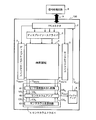
- FIG. 1 is a block diagram showing a schematic configuration of an active matrix substrate 100 provided in a liquid crystal display device according to an embodiment of the present invention.
- an active matrix substrate 100 includes a pixel region 1, a display gate driver 2, a display source driver 3, a sensor column driver 4, a sensor row driver 5, and a buffer amplifier 6 on a glass substrate.
- the FPC connector 7 is provided at least.
- a signal processing circuit 8 for processing an image signal captured by a light detection element (described later) in the pixel region 1 is connected to the active matrix substrate 100 via the FPC connector 7 and the FPC 9. .
- the above-described constituent members on the active matrix substrate 100 can be formed monolithically on the glass substrate by a semiconductor process. Or it is good also as a structure which mounted the amplifier and drivers among said structural members on the glass substrate by COG (Chip On Glass) technique etc., for example. Alternatively, it is conceivable that at least a part of the constituent members shown on the active matrix substrate 100 in FIG. 1 is mounted on the FPC 9.
- the active matrix substrate 100 is bonded to a counter substrate (not shown) having a counter electrode formed on the entire surface, and a liquid crystal material is sealed in the gap.
- the pixel area 1 is an area where a plurality of pixels are formed in order to display an image.
- an optical sensor for capturing an image is provided in each pixel in the pixel region 1.
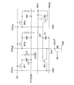
- FIG. 2 is an equivalent circuit diagram showing the arrangement of pixels and photosensors in the pixel region 1 of the active matrix substrate 100.
- one pixel is formed by three color picture elements of R (red), G (green), and B (blue).
- One photosensor composed of two photodiodes D1, D2, a capacitor CINT, and a thin film transistor M2 is provided.
- the pixel region 1 includes pixels arranged in a matrix of M rows ⁇ N columns and photosensors arranged in a matrix of M rows ⁇ N columns. As described above, the number of picture elements is M ⁇ 3N.
- the pixel region 1 has gate lines GL and source lines COL arranged in a matrix as wiring for the pixels.
- the gate line GL is connected to the display gate driver 2.
- the source line COL is connected to the display source driver 3.
- the gate lines GL are provided in M rows in the pixel region 1.
- three source lines COL are provided for each pixel in order to supply image data to the three picture elements in one pixel.
- a thin film transistor (TFT) M1 is provided as a pixel switching element at the intersection of the gate line GL and the source line COL.
- the thin film transistor M1 provided in each of the red, green, and blue picture elements is denoted as M1r, M1g, and M1b.
- the thin film transistor M1 has a gate electrode connected to the gate line GL, a source electrode connected to the source line COL, and a drain electrode connected to a pixel electrode (not shown).
- a liquid crystal capacitor LC is formed between the drain electrode of the thin film transistor M1 and the counter electrode (VCOM).
- an auxiliary capacitor LS is formed between the drain electrode and the TFTCOM.
- the pixel driven by the thin film transistor M1r connected to the intersection of one gate line GLi and one source line COLrj is provided with a red color filter corresponding to this pixel.
- red image data is supplied from the display source driver 3 via the source line COLrj, it functions as a red picture element.
- the pixel driven by the thin film transistor M1g connected to the intersection of the gate line GLi and the source line COLgj is provided with a green color filter so as to correspond to the picture element, and the display source is connected via the source line COLgj.
- green image data is supplied from the driver 3, it functions as a green picture element.
- the picture element driven by the thin film transistor M1b connected to the intersection of the gate line GLi and the source line COLbj is provided with a blue color filter so as to correspond to the picture element, and the display source is connected via the source line COLbj.
- blue image data is supplied from the driver 3, it functions as a blue picture element.
- the source line COLr also serves as the wiring VDD for supplying the constant voltage V DD from the sensor column driver 4 to the photosensor. Further, the source line COLg also serves as the sensor output wiring OUT.
- one photosensor is provided for each pixel (three picture elements) in the pixel region 1.
- the arrangement ratio of the pixels and the photosensors is not limited to this example and is arbitrary.
- one photosensor may be arranged for each picture element, or one photosensor may be arranged for a plurality of pixels.
- the photosensor includes a phototransistor (photo TFT) M4 as a photodetecting element, a capacitor CINT, and a thin film transistor M2 as a sensor switching element.
- the phototransistor M4 may have either a top gate structure or a bottom gate structure.
- the bottom gate structure is advantageous in that the manufacturing process can be simplified because the gate electrode functions as a light-shielding layer that blocks incident light from the backlight to the phototransistor M4.
- the gate and source of the phototransistor M4 are both connected to the reset wiring RST.
- the phototransistor M4 is not limited to a polysilicon TFT having high mobility, and an amorphous silicon TFT or a microcrystalline silicon TFT can be used. Note that the transistor M2 can also be realized by an amorphous silicon TFT or a microcrystalline silicon TFT. Therefore, the transistor M2 and the phototransistor M4 can be formed at the same time using the same material.
- the phototransistor M4 as the light detection element are as follows. That is, unlike a photodiode that requires the formation of a p-layer and an n-layer, the phototransistor M4 only needs to form one semiconductor layer (for example, an n-channel).
- the channel width which is an important parameter for determining the characteristics of the phototransistor, depends only on the accuracy of the semiconductor layer formation process or the accuracy of the gate width. For this reason, the phototransistor has less characteristic variation due to variation in accuracy of the manufacturing process than the photodiode. As a result, it is possible to realize a display device with a high-quality optical sensor with little variation in characteristics among sensors.
- the drain of the transistor M2 is connected to the wiring VDD, and the source is connected to the wiring OUT.
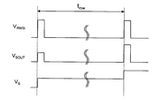
- the sensor row driver 5 sequentially selects a pair of wirings RSTi and RWSi shown in FIG. 2 at a predetermined time interval (t row ). As a result, the rows of photosensors from which signal charges are to be read out in the pixel region 1 are sequentially selected.
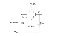
- the end of the wiring OUT is connected to the drain of the insulated gate field effect transistor M3. Further, the output wiring SOUT is connected to the drain of the transistor M3, and the potential V SOUT of the drain of the transistor M3 is output to the sensor column driver 4 as an output signal from the photosensor.
- the source of the transistor M3 is connected to the wiring VSS.
- the gate of the transistor M3 is connected to a reference voltage power supply (not shown) via the reference voltage wiring VB.
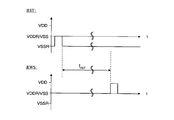
- FIG. 3 is a timing chart showing waveforms of a reset signal supplied from the wiring RST to the optical sensor and a readout signal supplied from the wiring RWS.
- FIG. 4 is a waveform diagram showing the relationship between input signals (RST, RWS) and V INT in the photosensor of the first embodiment.
- the high level V RST.H of the reset signal is equal to V SS .
- the high level V RWS.H of the read signal is equal to V DD and the low level V RWS.L is equal to V SS .
- the potential V INT of the gate electrode of the transistor M2 is expressed by the following equation (4).
- V INT V RST.H ⁇ V T, M2 ⁇ V RST ⁇ C SENSOR / C T (4)
- V T, M2 is the threshold voltage of the transistor M2
- ⁇ V RST is the pulse height of the reset signal (V RST.H -V RST.L )
- C SENSOR is the capacitance of the phototransistor M4. It is.
- C T is the sum of the capacitance of the capacitor C2, the capacitance C SENSOR of the phototransistor M4, and the capacitance C TFT of the transistor M2. Since V INT at this time is lower than the threshold voltage of the transistor M2, the transistor M2 is non-conductive in the reset period.
- the photocurrent integration period starts.
- a photocurrent proportional to the amount of light incident on the phototransistor M4 flows into the capacitor C2, and the capacitor C2 is discharged.
- the potential V INT of the gate of the transistor M2 at the end of the integration period is expressed by the following equation (5).
- V INT V RST.H ⁇ V T, M2 ⁇ V RST ⁇ C SENSOR / C T -I PHOTO ⁇ T INT / C T (5)
- I PHOTO is the photocurrent of the phototransistor M4
- T INT is the length of the integration period. Even during the integration period, since V INT is lower than the threshold voltage of the transistor M2, the transistor M2 is non-conductive.
- the readout signal RWS rises to start the readout period. Note that the read period continues while the read signal RWS is at a high level.
- charge injection occurs in the capacitor C2.
- the gate potential V INT of the transistor M2 is expressed by the following equation (6).
- V INT V RST.H ⁇ V T, M2 ⁇ V RST ⁇ C SENSOR / C T ⁇ I PHOTO ⁇ T INT / C T + ⁇ V RWS ⁇ C INT / C T (6)
- V RWS is the pulse height (V RWS.H ⁇ V RWS.L ) of the read signal.
- V INT of the gate of the transistor M2 becomes higher than the threshold voltage, so that the transistor M2 becomes conductive and functions as a source follower amplifier together with the bias transistor M3 provided at the end of the wiring OUT in each column.
- the sensor output voltage V PIX from the transistor M2 is proportional to the integrated value of the photocurrent of the phototransistor M4 during the integration period.
- the optical sensor output of each pixel can be obtained by periodically performing initialization by the reset pulse, integration of the photocurrent in the integration period, and reading of the sensor output in the readout period.
- the source lines COLr, COLg, and COLb are shared as the photosensor wirings VDD and OUT, so that the source lines COLr, COLg, and COLb are used as shown in FIG. Therefore, it is necessary to distinguish the timing for inputting the display image data signal from the timing for reading the sensor output.
- the sensor output is read using a horizontal blanking period or the like.
- the sensor column driver 4 includes a sensor pixel readout circuit 41, a sensor column amplifier 42, and a sensor column scanning circuit 43.
- a wiring SOUT (see FIG. 2) for outputting the sensor output V SOUT from the pixel region 1 is connected to the sensor pixel readout circuit 41.
- the sensor pixel readout circuit 41 outputs the peak hold voltage V Sj of the sensor output V SOUTj to the sensor column amplifier 42.
- V COUT is output to the buffer amplifier 6.
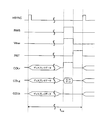
- FIG. 6 is a circuit diagram showing an internal configuration of the sensor pixel readout circuit 41.
- FIG. 7 is a waveform diagram showing the relationship between the readout signal V RWS , the sensor output V SOUT, and the output V S of the sensor pixel readout circuit.
- the transistor M2 is turned on to form a source follower amplifier by the transistors M2 and M3, and the sensor output V SOUT is output from the sensor pixel read circuit 41. Accumulated in the sample capacitor CSAM .
- the output voltage V S from the sensor pixel readout circuit 41 to the sensor column amplifier 42 during the row selection period (t row ) is shown in FIG. As shown, it is held at a level equal to the peak value of the sensor output V SOUT .
- each column amplifier is composed of transistors M6 and M7.
- the buffer amplifier 6 further amplifies V COUT output from the sensor column amplifier 42 and outputs it to the signal processing circuit 8 as a panel output (photosensor signal) V out .
- the sensor column scanning circuit 43 may scan the optical sensor columns one by one as described above, but is not limited thereto, and may be configured to interlace scan the optical sensor columns. Further, the sensor column scanning circuit 43 may be formed as a multi-phase driving scanning circuit such as a four-phase.
- the display device obtains a panel output V OUT corresponding to the amount of light received by the phototransistor M4 formed for each pixel in the pixel region 1.
- the panel output V OUT is sent to the signal processing circuit 8, A / D converted, and stored in a memory (not shown) as panel output data. That is, the same number of panel output data as the number of pixels (number of photosensors) in the pixel region 1 is stored in this memory.
- the signal processing circuit 8 performs various signal processing such as image capture and touch area detection using the panel output data stored in the memory.
- the same number of panel output data as the number of pixels (number of photosensors) in the pixel region 1 is accumulated in the memory of the signal processing circuit 8.
- the number of pixels is not necessarily limited due to restrictions such as memory capacity. It is not necessary to store the same number of panel output data.
- an optical sensor output can be obtained even when the phototransistor M4 is used instead of the conventional photodiode as the photodetecting element of the optical sensor.
- the transistor M2 and the phototransistor M4 are formed of amorphous silicon TFTs or microcrystalline silicon TFTs, there is an advantage that they can be manufactured at a lower cost than using polysilicon.
- the display device includes a phototransistor M5 instead of the phototransistor M4 described in the first embodiment as a light detection element in the photosensor. This is different from the first embodiment.
- the phototransistor M5 is the same as the phototransistor M4 in that the gate is connected to the reset wiring RST, but the source is connected to a wiring that supplies a second reset signal VRST different from the reset signal RST. This is different from the phototransistor M4.
- FIG. 10 is a waveform diagram showing the relationship between various signals applied to the photosensor according to the present embodiment and V INT .
- FIG. 11 is a waveform diagram showing changes in V INT when the potential drop of the reset signal RST is not steep in the configuration of the first embodiment as a comparative example.
- the configuration in which the wirings VDD and OUT connected to the photosensor are shared with the source wiring SL is exemplified. According to this configuration, there is an advantage that the pixel aperture ratio is high. However, the optical sensor wirings VDD and OUT may be provided separately from the source wiring SL.
- the present invention is industrially applicable as a display device having an optical sensor in a pixel region of an active matrix substrate.
Landscapes
- Engineering & Computer Science (AREA)
- General Engineering & Computer Science (AREA)
- Theoretical Computer Science (AREA)
- Human Computer Interaction (AREA)
- Physics & Mathematics (AREA)
- General Physics & Mathematics (AREA)
- Liquid Crystal (AREA)
- Position Input By Displaying (AREA)
- Control Of Indicators Other Than Cathode Ray Tubes (AREA)
- Devices For Indicating Variable Information By Combining Individual Elements (AREA)
- Liquid Crystal Display Device Control (AREA)
Abstract
Description
式(1)において、VFはフォトダイオードD1の順方向電圧、ΔVRSTは、リセット信号のパルスの高さ(VRST.H-VRST.L)であり、CPDはフォトダイオードD1の容量である。CTは、コンデンサC2の容量、フォトダイオードD1の容量CPDと、トランジスタM2の容量CTFTとの総和である。このときのVINTはトランジスタM2の閾値電圧より低いので、トランジスタM2はリセット期間において非導通状態となっている。
式(2)において、IPHOTOは、フォトダイオードD1の光電流、TINTは、積分期間の長さである。積分期間においても、VINTがトランジスタM2の閾値電圧より低いので、トランジスタM2は非導通状態となっている。
+ΔVRWS・CINT/CT …(3)
ΔVRWSは、読み出し信号のパルスの高さ(VRWS.H-VRWS.L)である。これにより、トランジスタM2のゲートの電位VINTが閾値電圧よりも高くなるので、トランジスタM2は導通状態となり、各列において配線OUTの端部に設けられているバイアストランジスタM3と共に、ソースフォロアアンプとして機能する。すなわち、トランジスタM2からのセンサ出力電圧VPIXは、積分期間におけるフォトダイオードD1の光電流の積分値に比例する。
本発明の一実施形態にかかる表示装置は、アクティブマトリクス基板の画素領域に光センサを備えた表示装置であって、前記光センサが、入射光を受光する光検出素子と、前記光検出素子に一方の電極が接続され、前記光検出素子からの出力電流を蓄積する容量と、当該光センサへリセット信号を供給するリセット信号配線と、当該光センサへ読み出し信号を供給する読み出し信号配線と、前記リセット信号が供給されてから前記読み出し信号が供給されるまでの間に前記容量に蓄積された出力電流を、前記読み出し信号にしたがって読み出すセンサスイッチング素子とを備え、前記光検出素子が、フォトトランジスタである。
式(4)において、VT,M2はトランジスタM2の閾値電圧、ΔVRSTは、リセット信号のパルスの高さ(VRST.H-VRST.L)であり、CSENSORはフォトトランジスタM4の容量である。CTは、コンデンサC2の容量、フォトトランジスタM4の容量CSENSORと、トランジスタM2の容量CTFTとの総和である。このときのVINTはトランジスタM2の閾値電圧より低いので、トランジスタM2はリセット期間において非導通状態となっている。
-IPHOTO・TINT/CT …(5)
式(5)において、IPHOTOは、フォトトランジスタM4の光電流、TINTは、積分期間の長さである。積分期間においても、VINTがトランジスタM2の閾値電圧より低いので、トランジスタM2は非導通状態となっている。
+ΔVRWS・CINT/CT …(6)
ΔVRWSは、読み出し信号のパルスの高さ(VRWS.H-VRWS.L)である。これにより、トランジスタM2のゲートの電位VINTが閾値電圧よりも高くなるので、トランジスタM2は導通状態となり、各列において配線OUTの端部に設けられているバイアストランジスタM3と共に、ソースフォロアアンプとして機能する。すなわち、トランジスタM2からのセンサ出力電圧VPIXは、積分期間におけるフォトトランジスタM4の光電流の積分値に比例する。
本発明の第2の実施形態にかかる表示装置について、以下に説明する。なお、上述の第1の実施形態において説明した構成と同様の機能を有する構成については、同じ参照符号を付記し、その詳細な説明を省略する。
2 ディスプレイゲートドライバ
3 ディスプレイソースドライバ
4 センサカラム(column)ドライバ
41 センサ画素読み出し回路
42 センサカラムアンプ
43 センサカラム走査回路
5 センサロウ(row)ドライバ
6 バッファアンプ
7 FPCコネクタ
8 信号処理回路
9 FPC
100 アクティブマトリクス基板
M2 薄膜トランジスタ(センサスイッチング素子)
M4 フォトトランジスタ(光検出素子)
Claims (6)
- アクティブマトリクス基板の画素領域に光センサを備えた表示装置であって、
前記光センサが、
入射光を受光する光検出素子と、
前記光検出素子に一方の電極が接続され、前記光検出素子からの出力電流を蓄積する容量と、
当該光センサへリセット信号を供給するリセット信号配線と、
当該光センサへ読み出し信号を供給する読み出し信号配線と、
前記リセット信号が供給されてから前記読み出し信号が供給されるまでの間に前記容量に蓄積された出力電流を、前記読み出し信号にしたがって読み出すセンサスイッチング素子とを備え、
前記光検出素子が、フォトトランジスタであることを特徴とする表示装置。 - 前記光検出素子がアモルファスシリコンTFTまたは微結晶シリコンTFTである、請求項1に記載の表示装置。
- 前記センサスイッチング素子がアモルファスシリコンTFTまたは微結晶シリコンTFTである、請求項1または2に記載の表示装置。
- 前記フォトトランジスタのゲートおよびソースが前記リセット信号配線に接続されている、請求項1~3のいずれか一項に記載の表示装置。
- 前記フォトトランジスタのゲートに前記リセット信号配線が接続され、当該フォトトランジスタのソースに当該フォトトランジスタがオフ状態になった後に電位降下を生じる第2のリセット信号配線が接続されている、請求項1~3のいずれか一項に記載の表示装置。
- 前記アクティブマトリクス基板に対向する対向基板と、
前記アクティブマトリクス基板と対向基板との間に挟持された液晶とをさらに備えた、請求項1~5のいずれか一項に記載の表示装置。
Priority Applications (6)
| Application Number | Priority Date | Filing Date | Title |
|---|---|---|---|
| RU2010149334/28A RU2473937C2 (ru) | 2008-06-03 | 2009-05-28 | Дисплейное устройство |
| US12/995,796 US20110080390A1 (en) | 2008-06-03 | 2009-05-28 | Display device |
| EP09758259.7A EP2287657A4 (en) | 2008-06-03 | 2009-05-28 | DISPLAY DEVICE |
| JP2010515847A JP5132771B2 (ja) | 2008-06-03 | 2009-05-28 | 表示装置 |
| BRPI0913338A BRPI0913338A2 (pt) | 2008-06-03 | 2009-05-28 | dispositivo de vídeo |
| CN2009801202953A CN102317840A (zh) | 2008-06-03 | 2009-05-28 | 显示装置 |
Applications Claiming Priority (2)
| Application Number | Priority Date | Filing Date | Title |
|---|---|---|---|
| JP2008146072 | 2008-06-03 | ||
| JP2008-146072 | 2008-06-03 |
Publications (1)
| Publication Number | Publication Date |
|---|---|
| WO2009147992A1 true WO2009147992A1 (ja) | 2009-12-10 |
Family
ID=41398069
Family Applications (1)
| Application Number | Title | Priority Date | Filing Date |
|---|---|---|---|
| PCT/JP2009/059769 WO2009147992A1 (ja) | 2008-06-03 | 2009-05-28 | 表示装置 |
Country Status (7)
| Country | Link |
|---|---|
| US (1) | US20110080390A1 (ja) |
| EP (1) | EP2287657A4 (ja) |
| JP (1) | JP5132771B2 (ja) |
| CN (1) | CN102317840A (ja) |
| BR (1) | BRPI0913338A2 (ja) |
| RU (1) | RU2473937C2 (ja) |
| WO (1) | WO2009147992A1 (ja) |
Cited By (1)
| Publication number | Priority date | Publication date | Assignee | Title |
|---|---|---|---|---|
| JP2012138572A (ja) * | 2010-12-10 | 2012-07-19 | Semiconductor Energy Lab Co Ltd | 光電変換素子、光電変換回路及び表示装置 |
Families Citing this family (9)
| Publication number | Priority date | Publication date | Assignee | Title |
|---|---|---|---|---|
| TWI414977B (zh) * | 2010-05-18 | 2013-11-11 | Au Optronics Corp | 觸控偵測方法及具有內嵌式觸控面板之平面顯示器 |
| KR102021908B1 (ko) | 2011-05-03 | 2019-09-18 | 삼성전자주식회사 | 광터치 스크린 장치 및 그 구동 방법 |
| KR101906971B1 (ko) | 2012-09-27 | 2018-10-11 | 삼성전자주식회사 | 하이브리드 터치 패널, 하이브리드 터치 스크린 장치 및 이의 구동 방법 |
| DE102013226633A1 (de) * | 2013-12-19 | 2015-06-25 | BSH Hausgeräte GmbH | Anzeige-Bedienfeld mit moduliertem Licht |
| CN103777422B (zh) * | 2013-12-27 | 2018-04-10 | 深圳市华星光电技术有限公司 | 液晶面板及其驱动方法、液晶显示器 |
| CN104200784B (zh) * | 2014-07-24 | 2017-07-28 | 京东方科技集团股份有限公司 | 像素驱动电路及其驱动方法、阵列基板、透反式显示装置 |
| KR102347825B1 (ko) * | 2017-08-16 | 2022-01-05 | 엘지디스플레이 주식회사 | 포토센서부를 포함하는 표시패널 및 그를 이용한 표시장치 |
| TWI692045B (zh) * | 2019-08-13 | 2020-04-21 | 大陸商集創北方(深圳)科技有限公司 | 觸控檢測模式切換方法、觸控顯示驅動整合晶片及資訊處理裝置 |
| JP7315452B2 (ja) * | 2019-12-20 | 2023-07-26 | 株式会社ジャパンディスプレイ | 光センサ装置 |
Citations (6)
| Publication number | Priority date | Publication date | Assignee | Title |
|---|---|---|---|---|
| JPH0611690A (ja) * | 1992-06-26 | 1994-01-21 | Rohm Co Ltd | 液晶表示装置 |
| JP2006003857A (ja) | 2003-08-25 | 2006-01-05 | Toshiba Matsushita Display Technology Co Ltd | 表示装置および光電変換素子 |
| JP2006079589A (ja) * | 2004-08-05 | 2006-03-23 | Sanyo Electric Co Ltd | タッチパネル |
| JP2007304245A (ja) * | 2006-05-10 | 2007-11-22 | Sony Corp | 液晶表示装置 |
| WO2007145346A1 (en) | 2006-06-12 | 2007-12-21 | Sharp Kabushiki Kaisha | Image sensor and display |
| WO2007145347A1 (en) | 2006-06-12 | 2007-12-21 | Sharp Kabushiki Kaisha | Combined image sensor and display device |
Family Cites Families (9)
| Publication number | Priority date | Publication date | Assignee | Title |
|---|---|---|---|---|
| GB9108226D0 (en) * | 1991-04-17 | 1991-06-05 | Philips Electronic Associated | Optical touch input device |
| JP4521176B2 (ja) * | 2003-10-31 | 2010-08-11 | 東芝モバイルディスプレイ株式会社 | 表示装置 |
| KR20060062164A (ko) * | 2004-12-03 | 2006-06-12 | 삼성전자주식회사 | 광센서를 내장하는 표시 장치 |
| JP4667079B2 (ja) * | 2005-03-07 | 2011-04-06 | シャープ株式会社 | 表示装置 |
| JP4510738B2 (ja) * | 2005-09-28 | 2010-07-28 | 株式会社 日立ディスプレイズ | 表示装置 |
| US20070182723A1 (en) * | 2006-01-31 | 2007-08-09 | Toshiba Matsushita Display Technology Co., Ltd. | Display device |
| JP2008102418A (ja) * | 2006-10-20 | 2008-05-01 | Toshiba Matsushita Display Technology Co Ltd | 表示装置 |
| JP2007310628A (ja) * | 2006-05-18 | 2007-11-29 | Hitachi Displays Ltd | 画像表示装置 |
| US8269746B2 (en) * | 2006-11-27 | 2012-09-18 | Microsoft Corporation | Communication with a touch screen |
-
2009
- 2009-05-28 JP JP2010515847A patent/JP5132771B2/ja not_active Expired - Fee Related
- 2009-05-28 EP EP09758259.7A patent/EP2287657A4/en not_active Withdrawn
- 2009-05-28 WO PCT/JP2009/059769 patent/WO2009147992A1/ja active Application Filing
- 2009-05-28 US US12/995,796 patent/US20110080390A1/en not_active Abandoned
- 2009-05-28 RU RU2010149334/28A patent/RU2473937C2/ru not_active IP Right Cessation
- 2009-05-28 BR BRPI0913338A patent/BRPI0913338A2/pt not_active IP Right Cessation
- 2009-05-28 CN CN2009801202953A patent/CN102317840A/zh active Pending
Patent Citations (6)
| Publication number | Priority date | Publication date | Assignee | Title |
|---|---|---|---|---|
| JPH0611690A (ja) * | 1992-06-26 | 1994-01-21 | Rohm Co Ltd | 液晶表示装置 |
| JP2006003857A (ja) | 2003-08-25 | 2006-01-05 | Toshiba Matsushita Display Technology Co Ltd | 表示装置および光電変換素子 |
| JP2006079589A (ja) * | 2004-08-05 | 2006-03-23 | Sanyo Electric Co Ltd | タッチパネル |
| JP2007304245A (ja) * | 2006-05-10 | 2007-11-22 | Sony Corp | 液晶表示装置 |
| WO2007145346A1 (en) | 2006-06-12 | 2007-12-21 | Sharp Kabushiki Kaisha | Image sensor and display |
| WO2007145347A1 (en) | 2006-06-12 | 2007-12-21 | Sharp Kabushiki Kaisha | Combined image sensor and display device |
Non-Patent Citations (2)
| Title |
|---|
| See also references of EP2287657A4 * |
| T. NAKAMURA ET AL.: "A Touch Panel Function Integrated LCD Including LTPS A/D Converter", SID 05 DIGEST, 2005, pages 1,054 - 1,055 |
Cited By (1)
| Publication number | Priority date | Publication date | Assignee | Title |
|---|---|---|---|---|
| JP2012138572A (ja) * | 2010-12-10 | 2012-07-19 | Semiconductor Energy Lab Co Ltd | 光電変換素子、光電変換回路及び表示装置 |
Also Published As
| Publication number | Publication date |
|---|---|
| CN102317840A (zh) | 2012-01-11 |
| JP5132771B2 (ja) | 2013-01-30 |
| RU2473937C2 (ru) | 2013-01-27 |
| JPWO2009147992A1 (ja) | 2011-10-27 |
| RU2010149334A (ru) | 2012-06-10 |
| US20110080390A1 (en) | 2011-04-07 |
| EP2287657A1 (en) | 2011-02-23 |
| BRPI0913338A2 (pt) | 2015-11-24 |
| EP2287657A4 (en) | 2013-07-03 |
Similar Documents
| Publication | Publication Date | Title |
|---|---|---|
| JP5132771B2 (ja) | 表示装置 | |
| JP5068320B2 (ja) | 表示装置 | |
| JP4799696B2 (ja) | 表示装置 | |
| WO2009148084A1 (ja) | 表示装置 | |
| US8416225B2 (en) | Display device | |
| US8759739B2 (en) | Optical sensor and display apparatus | |
| JP5284487B2 (ja) | 表示装置 | |
| US8658957B2 (en) | Sensor circuit and display apparatus | |
| US20100134452A1 (en) | Display device | |
| WO2010001929A1 (ja) | 表示装置 | |
| WO2010092709A1 (ja) | 表示装置 | |
| WO2010007890A1 (ja) | 表示装置 | |
| WO2010001652A1 (ja) | 表示装置 | |
| WO2010097984A1 (ja) | 光センサおよびこれを備えた表示装置 | |
| JP5421355B2 (ja) | 表示装置 | |
| WO2010100785A1 (ja) | 表示装置 | |
| WO2011013631A1 (ja) | 光センサおよび表示装置 | |
| WO2011145682A1 (ja) | 表示装置 |
Legal Events
| Date | Code | Title | Description |
|---|---|---|---|
| WWE | Wipo information: entry into national phase |
Ref document number: 200980120295.3 Country of ref document: CN |
|
| 121 | Ep: the epo has been informed by wipo that ep was designated in this application |
Ref document number: 09758259 Country of ref document: EP Kind code of ref document: A1 |
|
| WWE | Wipo information: entry into national phase |
Ref document number: 2010515847 Country of ref document: JP |
|
| WWE | Wipo information: entry into national phase |
Ref document number: 2009758259 Country of ref document: EP |
|
| WWE | Wipo information: entry into national phase |
Ref document number: 2010149334 Country of ref document: RU |
|
| WWE | Wipo information: entry into national phase |
Ref document number: 7832/CHENP/2010 Country of ref document: IN |
|
| NENP | Non-entry into the national phase |
Ref country code: DE |
|
| ENP | Entry into the national phase |
Ref document number: PI0913338 Country of ref document: BR Kind code of ref document: A2 Effective date: 20101201 |