WO2009147805A1 - 液晶光学素子の駆動方法、光ヘッド装置、及び、液晶光学素子 - Google Patents
液晶光学素子の駆動方法、光ヘッド装置、及び、液晶光学素子 Download PDFInfo
- Publication number
- WO2009147805A1 WO2009147805A1 PCT/JP2009/002369 JP2009002369W WO2009147805A1 WO 2009147805 A1 WO2009147805 A1 WO 2009147805A1 JP 2009002369 W JP2009002369 W JP 2009002369W WO 2009147805 A1 WO2009147805 A1 WO 2009147805A1
- Authority
- WO
- WIPO (PCT)
- Prior art keywords
- liquid crystal
- optical element
- light beam
- cover layer
- layer thickness
- Prior art date
- Legal status (The legal status is an assumption and is not a legal conclusion. Google has not performed a legal analysis and makes no representation as to the accuracy of the status listed.)
- Ceased
Links
Images









Classifications
-
- G—PHYSICS
- G11—INFORMATION STORAGE
- G11B—INFORMATION STORAGE BASED ON RELATIVE MOVEMENT BETWEEN RECORD CARRIER AND TRANSDUCER
- G11B7/00—Recording or reproducing by optical means, e.g. recording using a thermal beam of optical radiation by modifying optical properties or the physical structure, reproducing using an optical beam at lower power by sensing optical properties; Record carriers therefor
- G11B7/12—Heads, e.g. forming of the optical beam spot or modulation of the optical beam
- G11B7/135—Means for guiding the beam from the source to the record carrier or from the record carrier to the detector
- G11B7/1392—Means for controlling the beam wavefront, e.g. for correction of aberration
- G11B7/13925—Means for controlling the beam wavefront, e.g. for correction of aberration active, e.g. controlled by electrical or mechanical means
-
- G—PHYSICS
- G11—INFORMATION STORAGE
- G11B—INFORMATION STORAGE BASED ON RELATIVE MOVEMENT BETWEEN RECORD CARRIER AND TRANSDUCER
- G11B7/00—Recording or reproducing by optical means, e.g. recording using a thermal beam of optical radiation by modifying optical properties or the physical structure, reproducing using an optical beam at lower power by sensing optical properties; Record carriers therefor
- G11B7/12—Heads, e.g. forming of the optical beam spot or modulation of the optical beam
- G11B7/135—Means for guiding the beam from the source to the record carrier or from the record carrier to the detector
- G11B7/1372—Lenses
- G11B7/1378—Separate aberration correction lenses; Cylindrical lenses to generate astigmatism; Beam expanders
-
- G—PHYSICS
- G11—INFORMATION STORAGE
- G11B—INFORMATION STORAGE BASED ON RELATIVE MOVEMENT BETWEEN RECORD CARRIER AND TRANSDUCER
- G11B7/00—Recording or reproducing by optical means, e.g. recording using a thermal beam of optical radiation by modifying optical properties or the physical structure, reproducing using an optical beam at lower power by sensing optical properties; Record carriers therefor
- G11B2007/0003—Recording, reproducing or erasing systems characterised by the structure or type of the carrier
- G11B2007/0006—Recording, reproducing or erasing systems characterised by the structure or type of the carrier adapted for scanning different types of carrier, e.g. CD & DVD
Definitions
- the present invention relates to a method for driving a liquid crystal optical element, an optical head device, and a liquid crystal optical element, and more particularly to a cover layer up to a recording layer of an optical disc when a light beam having one type of wavelength is condensed on a plurality of types of optical discs.
- the present invention relates to a liquid crystal optical element driving method, an optical head device, and a liquid crystal optical element that perform aberration correction based on a deviation between the thickness of the lens and the corresponding cover layer thickness of the objective lens.
- optical disc apparatus that optically records information on an optical disc (optical recording medium) such as a CD (Compact Disc), a DVD (Digital Versatile Disc), or an MO (Magnetic Optical Disk) and reproduces the information recorded on the optical disc.
- optical disc optical recording medium
- high-capacity high-density optical discs such as HD (High Definition DVD) and BD (Blu-ray Disc) have also been developed.
- HD High Definition DVD
- BD Blu-ray Disc
- a semiconductor laser having a wavelength of 660 nm band is used as a light source.
- an objective lens having an NA (numerical aperture) of 0.6 to 0.65 is used.
- NA number of the NA
- a recording mark having a required size is formed in the information recording layer.
- a BD standard for recording / reproducing using a semiconductor laser having a wavelength of 405 nm and an objective lens having an NA of 0.85 has been proposed.
- an HD standard for recording / reproducing using a semiconductor laser having a wavelength of 405 nm and an objective lens having an NA of 0.65 has been proposed.
- the thickness of the cover layer of BD is 0.1 mm
- the thickness of the cover layer of HD is 0.6 mm. Therefore, the cover layer thickness of BD and HD is different. Therefore, when recording / reproducing both BD and HD optical discs with one optical disc apparatus, it is necessary to correct spherical aberration based on the difference in the cover layer thickness between BD and HD.
- an optical disc having a plurality of information recording layers (hereinafter referred to as a multilayer optical disc) has been proposed.
- the BD 2-layer standard and the HD 3-layer standard have been proposed.
- the practical cover layer thickness up to each information recording layer is different. Therefore, in order to record / reproduce a multilayer optical disc, an optical system such as an objective lens mounted on the optical disc apparatus is constructed so as to have a plurality of corresponding cover layer thicknesses according to the cover layer thickness of each information recording layer. There is a need to.
- the optical disc apparatus described in Patent Document 1 has a DVD-only lens and a CD-only lens mounted on a rotating two-lens actuator.
- the DVD and the CD are compatible by switching between the DVD dedicated lens and the CD dedicated lens.
- the optical disc device described in Patent Document 2 transmits a part of the light beam emitted from the red semiconductor laser as zero-order light and transmits a part of the light beam emitted from the red semiconductor laser as first-order diffracted light.
- the element is formed integrally with the objective lens. Then, the diffraction pattern of the hologram element is adjusted so that the objective lens integrated with the hologram element condenses the zero-order light on the DVD and the objective lens integrated with the hologram element condenses the first-order diffracted light on the CD. Designing.
- the hologram element transmits a part of the light beam emitted from the red semiconductor laser as the first-order diffracted light so as to correct the spherical aberration caused by the cover layer thickness difference between the CD and the DVD. This realizes reproduction compatibility of two types of optical discs having different cover layer thicknesses and NAs at one wavelength.
- a CD / DVD compatible reproducing optical pickup is equipped with a red semiconductor laser and an infrared semiconductor laser having a wavelength of 780 nm.
- CD-R the reflectance of the red semiconductor laser beam is significantly reduced and cannot be reproduced. Therefore, an infrared semiconductor laser is used for CD reproduction.
- the CD / DVD compatible reproduction optical pickup uses a compatible reproduction method that utilizes the fact that the wavelength of the light source used for reproduction differs between the CD and the DVD.
- CD-R playback was not essential, so a compatible DVD and CD playback system using only a red semiconductor laser was considered. Therefore, by applying the DVD and CD compatible playback method using only the red semiconductor laser, which was studied at the beginning of the development of the DVD playback optical pickup, the BD and HD compatible playback method using only the blue semiconductor laser was developed. There is a possibility.
- the shape of the objective lens in the range of NA necessary for condensing on a CD is formed so as to optimally condense to the cover layer thickness intermediate between DVD and CD, and condensing on CD. Therefore, the shape of the objective lens within the range of NA necessary for condensing on the DVD on the outer edge side from the range of NA necessary for the purpose is formed so as to optimally condense on the DVD. Thereby, compatibility with CD and DVD is aimed at.
- Patent Document 4 a liquid crystal optical element is used as an aberration correction element. Then, aberration correction and light amount control are performed simultaneously by the liquid crystal optical element.
- Patent Documents 5 and 6 a liquid crystal optical element is used as an aberration correction element. Then, the spherical aberration based on the cover layer thickness difference is reduced by the liquid crystal optical element. Thereby, compatibility between a plurality of types of optical disks having different cover layer thicknesses is achieved.
- the distance between the red semiconductor laser light source and the collimator lens is made variable.
- the degree of divergence of the light incident on the objective lens is changed, and the spherical aberration due to the difference in the cover layer thickness between the CD and the DVD is reduced. It is corrected. Thereby, compatibility with CD and DVD is aimed at.
- Patent Document 8 describes a liquid crystal optical element in which two or more layers of transparent electrode patterns are formed on one glass substrate.
- a transparent electrode for driving liquid crystal can be obtained by configuring a compatible technology for performing compatibility between BD and HD and a compatible technology for performing compatibility between a plurality of information recording layers in a multilayer optical disk using the technology described in Patent Document 4. It is necessary to increase the number of Specifically, two types of transparent electrodes are required: an electrode pattern for BD and an electrode pattern for HD. And if each electrode pattern is formed in two glass substrates, it is necessary to perform alignment of two electrode patterns with high precision. In addition, the number of transparent electrodes to be driven increases. In addition, although a plurality of electrode patterns may be formed on one glass substrate, the number of transparent electrodes to be driven increases.
- the present invention has been made to solve such a problem, and a liquid crystal capable of performing compatibility between a plurality of information recording layers in a plurality of types of multilayer optical disks without increasing the number of transparent electrodes of the liquid crystal optical element.
- An object is to provide a driving method of an optical element, an optical head device, and a liquid crystal optical element.
- a method for driving a liquid crystal optical element according to the present invention is a method for driving a liquid crystal optical element in an optical head device that condenses a light beam from a light source with a first numerical aperture onto a first multilayer optical disk having a first cover layer thickness. It is.
- the optical head device is divided into a plurality of regions by an objective optical element for condensing a light beam from the light source onto the first multilayer optical disc and a plurality of concentric circular electrodes having different sizes.
- a liquid crystal optical element including the liquid crystal layer and an actuator for defocusing the objective optical element.
- the plurality of transparent electrodes may reduce spherical aberration based on a difference in cover layer thickness of each information recording layer of the first multilayer optical disc in the plurality of regions in the light beam transmitted through the liquid crystal optical element. It is formed with an electrode pattern that gives a phase difference.
- the objective optical element is defocused by the actuator, and a phase difference imparted to a light beam transmitted through the liquid crystal optical element by the plurality of regions is the liquid crystal optical element.
- a voltage is applied to the plurality of transparent electrodes so as to decrease from the center of the element toward the outer periphery.
- the plurality of regions have the second cover layer thickness larger than the first cover layer thickness in the light beam transmitted through the liquid crystal optical element, and the first numerical aperture is greater than the first numerical aperture.
- a phase difference is provided so as to reduce spherical aberration based on the cover layer thickness difference of each information recording layer of the second multilayer optical disc in which the light beam from the light source is collected with a small second numerical aperture.
- the optical head device is an optical head device for condensing a light beam from a light source with a first numerical aperture on a first multilayer optical disk having a first cover layer thickness.
- An optical head device includes an objective optical element for condensing a light beam from the light source onto the first multilayer optical disk, and a plurality of circular transparent electrodes having different sizes arranged concentrically.
- a liquid crystal optical element including a liquid crystal layer divided into a plurality of regions, and an actuator for defocusing the objective optical element.
- the plurality of transparent electrodes may reduce spherical aberration based on a difference in cover layer thickness of each information recording layer of the first multilayer optical disc in the plurality of regions in the light beam transmitted through the liquid crystal optical element.
- the objective optical element is defocused by the actuator, and the phase difference that the plurality of regions impart to the light beam transmitted through the liquid crystal optical element decreases from the center of the liquid crystal optical element toward the outer periphery.
- the plurality of regions have the second cover layer thickness that is larger than the first cover layer thickness in the light beam transmitted through the liquid crystal optical element.
- the spherical aberration based on the cover layer thickness difference of each information recording layer of the second multilayer optical disc in which the light beam from the light source is collected with a second numerical aperture smaller than the first numerical aperture is reduced. It gives a phase difference.
- the liquid crystal optical element according to the present invention includes a plurality of circular transparent electrodes having different sizes arranged concentrically and a liquid crystal layer divided into a plurality of regions by the plurality of transparent electrodes.
- the plurality of regions have a first cover layer thickness for a light beam transmitted through the liquid crystal optical element, and a light beam from a light source is condensed with a first numerical aperture.
- the first multi-layer optical disk is formed with an electrode pattern that gives a phase difference that reduces spherical aberration based on the thickness difference of the cover layer of each information recording layer.
- the plurality of regions When a voltage is applied to the plurality of transparent electrodes so that a phase difference imparted to a light beam transmitted through the liquid crystal optical element by the plurality of regions decreases from the center to the outer periphery of the liquid crystal optical element.
- the plurality of regions have a second cover layer thickness larger than the first cover layer thickness in a light beam transmitted through the liquid crystal optical element, and a second smaller than the first numerical aperture.
- a phase difference is provided so as to reduce spherical aberration based on the cover layer thickness difference of each information recording layer of the second multilayer optical disc on which the light beam from the light source is condensed with a numerical aperture.
- the cover of each information recording layer of the second multilayer optical disc is used by using the transparent electrode formed so as to reduce the spherical aberration based on the thickness difference of the cover layer of each information recording layer of the first multilayer optical disc.
- Spherical aberration based on the layer thickness difference can be reduced.
- the liquid crystal optical element includes a plurality of first transparent electrodes and a plurality of second transparent electrodes.
- the plurality of first transparent electrodes have a plurality of circular transparent electrodes of different sizes arranged concentrically, and divide the liquid crystal layer into a plurality of first regions.
- the plurality of second transparent electrodes have a plurality of circular transparent electrodes of different sizes arranged concentrically, and divide the liquid crystal layer into a plurality of second regions.
- the plurality of first regions have a thickness of the first cover layer on a light beam transmitted through the liquid crystal optical element, and a light beam from the light source is condensed with the first numerical aperture.
- a light beam from the light source is collected with a second numerical aperture smaller than the first numerical aperture, the optical disc having one optical disc and the second cover layer thicker than the first cover layer. It is preferable to provide a phase difference that reduces spherical aberration based on the cover layer thickness difference with the second optical disc. Further, the plurality of second regions give a phase difference that reduces spherical aberration based on a cover layer thickness difference of each information recording layer of the first multilayer optical disc to the light beam transmitted through the liquid crystal optical element. It is preferable to do. In the plurality of second regions, the objective optical element is defocused by the actuator, and a phase difference that the plurality of second regions imparts to a light beam transmitted through the liquid crystal optical element is the liquid crystal optical element.
- each information recording layer of the second multilayer optical disc is transmitted to the light beam transmitted through the liquid crystal optical element. It is preferable to provide a phase difference that reduces spherical aberration based on the cover layer thickness difference. As a result, compatibility between a plurality of types of optical disks having different cover layer thickness differences can be performed.
- the objective optical element has a surface shape that favorably collects a light beam on an optical disc having a predetermined cover layer thickness between the first cover layer thickness and the second cover layer thickness. It is preferable.
- the plurality of first regions include a difference in cover layer thickness between the predetermined cover layer thickness and the first cover layer thickness or the second cover layer thickness in a light beam transmitted through the liquid crystal optical element. It is preferable to provide a phase difference that reduces spherical aberration based on the above. As a result, the sign of spherical aberration that occurs when the objective optical element focuses on the optical disk having the first cover layer thickness, and the objective optical element that occurs when the objective optical element focuses on the optical disk having the second cover layer thickness.
- the liquid crystal optical element shifts the phase difference imparted to the light beam by 1 ⁇ from the phase difference to be imparted in order to reduce the spherical aberration.
- the width of the voltage to be applied to the optical element can be reduced.
- the plurality of first regions include a light beam that passes through the liquid crystal optical element within a range of the second numerical aperture, and is approximately (m / n) ⁇ (where n is a natural number satisfying n ⁇ 2, m Is an integer satisfying
- the plurality of first regions are arranged in the above-described cases when the light from the light source is condensed on the first optical disc and when the light from the light source is condensed on the second optical disc. It is preferable to add the phase difference by changing the sign of the phase difference.
- the liquid crystal optical element is preferably held integrally with the objective optical element by an actuator. Thereby, even if a lens shift occurs, the influence of the lens shift on the liquid crystal optical element can be reduced.
- the objective optical element is sandwiched between a glass substrate and an objective lens that favorably focuses the light beam from the light source on the first optical disk having the first cover layer thickness with the first numerical aperture.
- a liquid crystal lens including a transparent electrode that drives the liquid crystal layer.
- the liquid crystal layer of the liquid crystal lens has a second cover layer thickness by which the light beam transmitted through the liquid crystal lens has the second cover layer thickness by the objective lens. It is preferable to adjust the divergence angle of the light beam transmitted through the liquid crystal lens so that the light beam is condensed at the second numerical aperture.
- the liquid crystal lens preferably includes two liquid crystal layers, and the alignment direction of the liquid crystal layer of one of the liquid crystal lenses is orthogonal to the alignment direction of the other liquid crystal layer. Thereby, the liquid crystal lens can act on both incident light incident on the optical disc and reflected light reflected from the optical disc.
- the objective optical element includes a first objective lens that favorably concentrates a light beam from the light source on the first optical disc having the first cover layer thickness with the first numerical aperture, and the second objective lens. And a second objective lens that favorably focuses the light beam from the light source with the second numerical aperture on a second optical disc having a cover layer thickness of It is preferable that an optical path switching mechanism for guiding a light beam emitted from the liquid crystal optical element to the first objective lens or the second objective lens is provided between the liquid crystal optical element and the objective optical element. .
- the liquid crystal optical element preferably includes two liquid crystal layers, and the alignment direction of one liquid crystal layer of the liquid crystal optical element is orthogonal to the alignment direction of the other liquid crystal layer.
- the liquid crystal optical element can act on both incident light incident on the optical disk and reflected light reflected from the optical disk.
- compatibility between a plurality of information recording layers in a plurality of types of multilayer optical disks can be performed without increasing the number of transparent electrodes of the liquid crystal optical element.
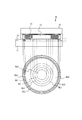
- 1 shows an example of a liquid crystal optical element according to the present invention.
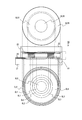
- 2 shows an example of a liquid crystal optical element according to Comparative Example 1. It is a graph showing the spherical aberration at the time of condensing a light beam to 2 layer BD using the liquid crystal optical element concerning the comparative example 1.
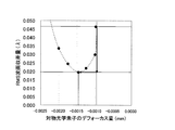
- 6 is a graph showing spherical aberration when a light beam is condensed on a two-layer HD using the liquid crystal optical element according to Comparative Example 1. It is a graph showing the relationship between the spherical aberration and the defocus amount when the light beam is condensed on the two-layer HD using the liquid crystal optical element according to the present invention.
- FIG. 6 is a cross-sectional view illustrating an example of a liquid crystal lens according to Example 2.
- FIG. 6 is a cross-sectional view showing an example of a liquid crystal optical element according to Example 2.
- FIG. 6 is a schematic diagram illustrating an example of an optical head device according to a second embodiment.
- FIG. 6 is a diagram for explaining the operation of a liquid crystal lens according to Example 2.
- FIG. 6 is a diagram for explaining the operation of a liquid crystal lens according to Example 2.
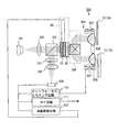
- FIG. 6 is a schematic diagram illustrating an example of an optical head device according to a third embodiment.
- RMS root mean square wavefront aberration
- the wavefront aberration is a deviation of the wavefront shape of the light beam transmitted through the lens from the wavefront shape of the light beam transmitted through the ideal lens.
- the deviation expressed as a standard deviation is called RMS wavefront aberration.
- the Marechal condition is that “when the normalized intensity at the diffraction focus F is 0.8 or more, the system is sufficiently corrected”. This is equivalent to “the standard deviation of the deviation (RMS wavefront aberration) between the wavefront and the reference spherical surface having the center at the diffraction focal point is ⁇ / 14 or less”.
- the liquid crystal optical element 10 includes a first substrate 11, a second substrate 12, a liquid crystal layer 13, an upper transparent electrode 14, a lower transparent electrode 15, and the like.
- the liquid crystal layer 13 is sandwiched between the first substrate 11 and the second substrate 12. Specifically, the liquid crystal layer 13 is formed by sealing liquid crystal in a space formed by a first substrate 11, a second substrate 12, and a seal as a spacer.
- the upper transparent electrode 14 is formed on the liquid crystal layer side surface of the first substrate 11.
- the lower transparent electrode 15 is formed on the surface of the second substrate 12 on the liquid crystal layer side. Accordingly, the liquid crystal layer 13 is sandwiched between the upper transparent electrode 14 and the lower transparent electrode 15.
- the electrode pattern of the upper transparent electrode 14 and the electrode pattern of the lower transparent electrode 15 are the same.
- the electrode patterns of the upper transparent electrode 14 and the lower transparent electrode 15 are electrode patterns for correcting spherical aberration of the two-layer BD (first multilayer optical disc).
- the electrode pattern of the upper transparent electrode 14 and the lower transparent electrode 15 is a pattern in which a plurality of transparent electrodes formed in different sizes are arranged concentrically. ing. Different voltages are applied to the circular transparent electrodes. Therefore, the alignment direction of the liquid crystal driven by each transparent electrode is different. Accordingly, the phase difference generated in the light beam transmitted through the liquid crystal layer 13 driven by each transparent electrode is also different.
- the liquid crystal layer 13 is divided into nine regions by the nine transparent electrodes.
- the innermost area is a circular area. Further, the other eight regions are in a ring shape.
- the liquid crystal layer 13 in the innermost region and the outermost region generates a phase difference of OL0 in the light beam transmitted through the region.
- the liquid crystal layer 13 in the second region and the sixth region from the center generates a phase difference of OL1 in the light beam transmitted through the region.
- the liquid crystal layer 13 in the third region and the seventh region from the center generates a phase difference of OL2 in the light beam that passes through the region.
- the liquid crystal layers 13 in the fourth and eighth regions from the center generate a phase difference of OL3 in the light beam transmitted through the region.
- the liquid crystal layer 13 in the fifth region from the center generates a phase difference of OL4 in the light beam transmitted through the region.
- the liquid crystal optical element 10 is a spherical surface based on the difference in the cover layer thickness of each information recording layer of the two-layer BD. Aberration is corrected.
- the transparent electrode is formed on the first substrate 11 and the second substrate 12 by a general vapor deposition method, a sputtering method, or the like. Specifically, first, a transparent electrode film such as indium tin oxide (ITO) is formed on the first substrate 11 and the second substrate 12. Next, the transparent electrode film is etched into a desired pattern by photolithography / etching or the like. As the transparent electrode film material, other materials such as zinc tin oxide (ZnO) may be used.
- ITO indium tin oxide
- ZnO zinc tin oxide
- the liquid crystal optical element 20 according to the comparative example 1 applies the conventional technique to perform compatibility between BD and HD, compatibility between information recording layers of the multilayer BD, and compatibility between information recording layers of the multilayer HD. It is assumed as a liquid crystal optical element.
- the liquid crystal optical element 20 according to Comparative Example 1 includes a first substrate 21, a second substrate 22, a liquid crystal layer 23, an upper transparent electrode 24, a lower transparent electrode 25, and the like.
- the liquid crystal optical element 20 concerning the comparative example 1 differs from the liquid crystal optical element 10 of this invention only in the structure of the upper surface transparent electrode 24.
- FIG. Since the other structure of the liquid crystal optical element 20 according to the comparative example 1 is almost the same as that of the liquid crystal optical element 10 of the present invention, the description thereof is omitted.
- the electrode pattern of the upper transparent electrode 24 and the electrode pattern of the lower transparent electrode 25 are different from the liquid crystal optical element 10 according to the present invention.
- the electrode pattern of the lower transparent electrode 25 is an electrode pattern for correcting the spherical aberration of the two-layer BD, like the lower transparent electrode 15 of the liquid crystal optical element 10 according to the present invention.
- the electrode pattern of the lower transparent electrode 25 is a pattern in which a plurality of transparent electrodes formed in circular shapes having different sizes are arranged concentrically.
- the liquid crystal layer 23 is divided into a plurality of regions by the plurality of transparent electrodes. The liquid crystal layer 23 in each region generates a phase difference of OL0, OL1, OL2, OL3, and OL4 in the light beam that passes through the region.
- the liquid crystal optical element 20 has a spherical surface based on the difference in cover layer thickness of each information recording layer of the two-layer BD. Aberration is corrected.
- the electrode pattern of the upper surface transparent electrode 24 is a pattern in which a plurality of transparent electrodes formed in circular shapes having different sizes are arranged concentrically. Further, the liquid crystal layer 23 is divided into a plurality of regions by the plurality of transparent electrodes. Specifically, on the surface (upper surface) of the liquid crystal layer 23 on the first substrate 21 side, two transparent electrodes formed in circular shapes having different sizes are arranged concentrically. The liquid crystal layer 23 is divided into three regions by the two transparent electrodes. The innermost area is a circular area. Further, the other two regions have a ring shape. By being driven by the transparent electrode, the liquid crystal layer 23 in the innermost region and the outermost region generates a phase difference of OL00 in the light beam that passes through the region.
- the liquid crystal layer 23 in the second region from the center generates a phase difference of OL01 in the light beam transmitted through the region. Then, by generating two kinds of phase differences OL00 and OL01 in the light beam transmitted through the liquid crystal optical element 20, the liquid crystal optical element 20 covers the information recording layers of the two-layer HD (second multilayer optical disc). Spherical aberration based on the difference in layer thickness is corrected.
- the numerical aperture of HD (second numerical aperture) is smaller than the numerical aperture of BD (first numerical aperture). Therefore, the range of the liquid crystal layer 23 where the phase difference has to be generated is narrower than that of the liquid crystal layer 13.
- spherical aberration is proportional to the fourth power of the numerical aperture. Therefore, the spherical aberration based on the difference in the cover layer thickness of each information recording layer of the two-layer HD is smaller than the spherical aberration based on the difference in the cover layer thickness of each information recording layer of the two-layer BD. Therefore, even if the electrode pattern of the upper transparent electrode 24 is simpler than the electrode pattern of the upper transparent electrode 14, the liquid crystal optical element 20 can sufficiently correct the spherical aberration.
- the objective optical element includes an objective lens and the like.
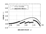
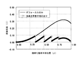
- FIG. 3A shows the spherical aberration that occurs when the light beam is condensed on the two-layer BD
- FIG. 3B shows the spherical aberration that occurs when the light beam is condensed on the two-layer HD.
- the vertical axis indicates the wavefront aberration ( ⁇ ), and the horizontal axis indicates the normalized radial radius position ( ⁇ ).
- the wavefront aberration represents the magnitude of spherical aberration that occurs when the light beam is condensed on the two-layer BD or the two-layer HD using the liquid crystal optical element 20.
- the solid line indicates the wavefront aberration when the liquid crystal optical element 20 is not driven, and the plot point with a circle indicates the wavefront aberration when the liquid crystal optical element 20 is driven. Indicates.
- spherical aberration based on the cover layer thickness difference of the information recording layer is reduced by defocusing the objective optical element.
- the RMS wavefront aberration is 128 m ⁇ in the two-layer BD, and 46.5 m ⁇ in the two-layer HD, and the Marechal condition ( ⁇ / 14 or less, that is, 35 m ⁇ or less).
- the liquid crystal optical element 20 is driven at this defocus position, the RMS wavefront aberration is reduced to 25.9 m ⁇ in the two-layer BD, and the RMS wavefront aberration is reduced to 22.5 m ⁇ in the two-layer HD.
- the liquid crystal optical element 20 according to the comparative example 1 can also perform compatibility between BD and HD and information recording layers in each of the two-layer BD and the two-layer HD.
- the electrode patterns of the upper transparent electrode 24 and the lower transparent electrode 25 are different. Therefore, it is necessary that the alignment accuracy of the two types of electrode patterns is very high. Further, the number of extraction electrodes for applying a voltage to each transparent electrode increases. Therefore, in the embodiment of the present invention, the liquid crystal optical element 10 that can also perform compatibility between the information recording layers of the two-layer HD is provided using an electrode pattern that performs compatibility between the information recording layers of the two-layer BD.
- FIG. 4 is a graph showing the relationship between the spherical aberration and the defocus amount.
- the vertical axis represents the RMS wavefront aberration amount ( ⁇ )
- the horizontal axis represents the defocus amount of the objective optical element.
- the RMS wavefront aberration amount represents the magnitude of spherical aberration that occurs when the liquid crystal optical element 10 is used to focus the light beam on the two-layer HD.
- the rightmost plot point (the plot point where the defocus amount is ⁇ 0.0010 mm) toward the paper surface is a state where no voltage is applied to the transparent electrode of the liquid crystal optical element 10 (liquid crystal optical).
- the RMS wavefront aberration amount in a state where the element 10 is not driven is shown.
- the other plot points represent the RMS wavefront aberration amount when a voltage is applied to the transparent electrode of the liquid crystal optical element 10.
- the RMS wavefront aberration amount changes. Specifically, as the objective optical element is defocused, the RMS wavefront aberration amount gradually decreases and becomes minimal and then gradually increases. The RMS wavefront aberration amount is minimized when the defocus amount is -0.00145 mm.
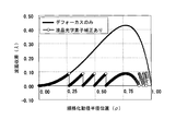
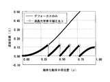
- Wavefront aberrations of the liquid crystal optical element 10 at the defocus amounts at the respective plot points shown in FIG. 4 are shown in FIGS. 5 to 9, the vertical axis represents the wavefront aberration ( ⁇ ), and the horizontal axis represents the normalized radial radius position ( ⁇ ).
- the wavefront aberration represents the magnitude of spherical aberration that occurs when the light beam is condensed on the two-layer HD using the liquid crystal optical element 10.
- the solid line indicates the wavefront aberration when the liquid crystal optical element 10 is not driven, and the plotted points with ⁇ indicate the wavefront aberration when the liquid crystal optical element 10 is driven.
- the defocus amounts in FIGS. 5, 6, 7, 8, and 9 are about ⁇ 0.0010 mm, about ⁇ 0.0013 mm, about ⁇ 0.0015 mm, about ⁇ 0.0018 mm, and about ⁇ 0.0020 mm.
- the RMS wavefront aberration amount is suppressed to about 30 m ⁇ or less. be able to.
- the gradient of the wavefront aberration shape when the liquid crystal optical element 10 is not driven becomes gentle.
- the amount of phase aberration imparted to the light beam in the liquid crystal layer 13 between adjacent transparent electrodes is decreased from the center of the liquid crystal optical element 10 toward the outer periphery, thereby correcting the spherical aberration. Found that it will grow.
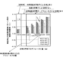
- FIG. 10 shows the relationship between the phase amount imparted to the light beam in the liquid crystal layer 13 between the adjacent transparent electrodes and the defocus amount of the objective optical element when condensing the light beam on the two-layer HD.
- the vertical axis represents the phase amount imparted to the light beam in the liquid crystal layer 13 between adjacent transparent electrodes (that is, the phase amount imparted to the light beam by each region of the liquid crystal layer 13), and the horizontal axis represents The defocus amount of the objective optical element is shown.
- the leftmost side of the paper surface of FIG. 10 when the light beam is condensed on the two-layer HD using the liquid crystal optical element 20 according to the comparative example 1, the light beam is emitted in the liquid crystal layer 23 between the adjacent transparent electrodes.
- the phase amount to be given to is shown.
- the pattern of the upper transparent electrode 24 is designed so that the phase amount imparted to the light beam in the liquid crystal layer 23 between adjacent transparent electrodes is substantially the same.
- the phase amount imparted to the light beam in the liquid crystal layer 13 between the adjacent transparent electrodes is defocused, and the phase amount increases from the center of the liquid crystal optical element 10 toward the outer periphery. Less.
- the liquid crystal optical element 10 according to the embodiment of the present invention can be used for condensing a light beam on the two-layer HD without having an electrode pattern for compatibility between the information recording layers of the two-layer HD.
- RMS wavefront aberration can be reduced to about 20 m ⁇ .
- the liquid crystal optical element 10 uses an electrode pattern for compatibility between the information recording layers of the two-layer BD. Compatibility between the information recording layers of the two-layer HD can be performed.
- FIG. 11A, FIG. 11B, FIG. 12A, and FIG. 12B show an example of the objective optical element 90 according to the present invention.
- the objective optical element 90 includes a liquid crystal optical element 10, a liquid crystal optical element 30, an objective lens 6, and the like.
- the liquid crystal optical element 30 corrects spherical aberration based on the cover layer thickness difference between BD and HD.
- a liquid crystal optical element 30 that corrects spherical aberration based on a cover layer thickness difference between BD and HD may be added to the objective optical element 90.
- the liquid crystal optical element 10 is disposed on the laser light source (not shown) side.
- the liquid crystal optical element 30 is disposed between the liquid crystal optical element 10 and the objective lens 6.
- the liquid crystal optical element 10 and the liquid crystal optical element 30 may be integrally formed.
- the surface of the objective lens 6 on the liquid crystal optical element 30 side is divided into a central portion 6A and an outer peripheral portion 6B.
- the central portion 6A is a circular region having the same size as the HD NA (numerical aperture).
- the outer peripheral part 6B is an annular area provided on the outer peripheral side of the central part 6A.
- the central portion 6A favorably emits a light beam to an optical disc having a predetermined cover layer thickness between the BD cover layer thickness (first cover layer thickness) and the HD cover layer thickness (second cover layer thickness). It has a surface shape for condensing light.
- the outer peripheral portion 6B has a surface shape that favorably collects a light beam with respect to a BD having a cover layer thickness of 0.1 mm.
- the liquid crystal optical element 30 has substantially the same configuration as the liquid crystal optical element 10.
- the liquid crystal optical element 30 is a spherical surface based on a cover layer thickness difference between a predetermined cover layer thickness of the optical disc on which the light beam transmitted through the central portion 6A of the objective lens 6 is well collected and a cover layer thickness of BD or HD. Correct aberrations.
- FIG. 11A shows an objective optical element 90 that condenses the light flux on the single layer HD 71
- FIG. 11B shows an objective optical element 90 that condenses the light flux on the multilayer HD 72
- FIG. 12A collects the light flux on the single layer BD 73
- FIG. 12B shows the objective optical element 90 that focuses the light beam on the multilayer BD 74.
- the advancing direction of a light beam is shown with a broken line.
- solid lines L1, L2, L3, and L4 indicate the wavefront shapes of the light beams.
- the light beam transmitted through the outer peripheral portion 6B of the objective lens 6 is not condensed on the single layer HD71.
- the outer peripheral portion 6B has a surface shape that favorably collects the light beam transmitted through the outer peripheral portion 6B with respect to the single layer BD73. Therefore, the light beam transmitted through the outer peripheral portion 6B has a large spherical aberration on the single layer HD71. Therefore, the light beam transmitted through the outer peripheral portion 6B is not condensed on the single layer HD71.
- the liquid crystal optical element 30 When the liquid crystal optical element 30 is driven, a phase difference is generated in the light beam that passes through a range corresponding to the NA of the HD of the liquid crystal optical element 30.
- the wavefront shape of the light beam transmitted through the range corresponding to the HD NA of the liquid crystal optical element 30 is different from the wavefront shape of the light beam transmitted outside the range corresponding to the HD NA of the liquid crystal optical element 30.
- the phase difference corrects spherical aberration based on the cover layer thickness difference between the predetermined cover layer thickness of the optical disc on which the light beam transmitted through the central portion 6A of the objective lens 6 is well collected and the HD cover layer thickness. It is the size to do.
- the liquid crystal optical element 30 causes the light flux that passes through the range corresponding to the NA of the HD of the liquid crystal optical element 30 to generate the phase difference, thereby condensing the light flux on the information recording surface of the single layer HD 71 satisfactorily.
- both the liquid crystal optical element 10 and the liquid crystal optical element 30 are driven. Similar to the case where the light beam is condensed on the single layer HD 71, the light beam transmitted through the outer peripheral portion 6 ⁇ / b> B of the objective lens 6 is not condensed on the multilayer HD 72. Similarly to the case where the light beam is condensed on the single layer HD 71, the liquid crystal optical element 30 is driven to generate a phase difference in the light beam that passes through a range corresponding to the NA of the HD of the liquid crystal optical element 30.
- the phase difference corrects spherical aberration based on the cover layer thickness difference between the predetermined cover layer thickness of the optical disc on which the light beam transmitted through the central portion 6A of the objective lens 6 is well collected and the HD cover layer thickness. It is the size to do.
- the objective optical element 90 is appropriately defocused. Specifically, the objective optical element 90 is defocused so that the RMS wavefront aberration amount in FIG. 4 is less than 30 m ⁇ and the gradient of the wavefront shape of the wavefront aberration in FIGS.
- the liquid crystal optical system is such that the phase amount imparted to the light flux in the liquid crystal layer 13 between adjacent transparent electrodes decreases from the center of the liquid crystal optical element 10 toward the outer periphery.
- a voltage is applied to each transparent electrode of the element 10.
- the liquid crystal optical element 30 when the light beam is condensed on the single layer BD 73, only the liquid crystal optical element 30 is driven, and the liquid crystal optical element 10 is not driven. Then, by driving the liquid crystal optical element 30, a phase difference is generated in the light beam transmitted through the liquid crystal optical element 30.
- the phase difference corrects the spherical aberration based on the cover layer thickness difference between the predetermined cover layer thickness of the optical disc on which the light beam transmitted through the central portion 6A of the objective lens 6 is well collected and the cover layer thickness of the BD. It is a big size.
- the liquid crystal optical element 30 causes the light flux that passes through the liquid crystal optical element 30 to generate the phase difference, thereby favorably condensing the light flux on the information recording surface of the single layer BD73.
- the outer peripheral portion 6B has a surface shape that favorably collects the light beam transmitted through the outer peripheral portion 6B with respect to the single layer BD73. Therefore, the light beam transmitted through the outer peripheral portion 6B has almost no spherical aberration on the single layer BD73. Therefore, the light beam transmitted through the entire surface of the objective lens 6 is condensed on the single layer BD73.
- the predetermined cover layer thickness of the optical disc on which the light beam passing through the central portion 6A of the objective lens 6 is well collected is an intermediate cover layer thickness between the BD cover layer thickness and the HD cover layer thickness.
- the spherical aberration that occurs when the light beam is condensed on the BD by the objective lens 6 and the spherical aberration that occurs when the light beam is condensed on the HD by the objective lens 6 are absolute only by reversing the sign. The values are equal.
- the liquid crystal optical element 30 is driven by giving the phase difference to be given with a shift of 1 ⁇ . It is possible to reduce the amount of voltage required to do this. This is because in wave optics, the phase lag and phase advance of 1 ⁇ are the same as those in which no phase lag and phase advance occur.
- the predetermined cover layer thickness of the optical disc on which the light beam transmitted through the central portion 6A of the objective lens 6 is favorably collected is an intermediate cover layer thickness between the BD cover layer thickness and the HD cover layer thickness.
- the sign of the phase difference given to the light beam transmitted through the liquid crystal optical element 30 is plus.
- the sign of the phase difference to be given to the light beam transmitted through the liquid crystal optical element 30 is negative.
- the phase difference generated in the light beam transmitted through the liquid crystal optical element 30 is shifted by + 1 ⁇ from the phase difference to be applied. More specifically, when the light beam is condensed on the single layer HD 71, when the phase difference applied to the light beam transmitted through the liquid crystal optical element 30 is 0.4 ⁇ , the liquid crystal is collected when the light beam is condensed on the single layer BD73. The phase difference to be given to the light beam transmitted through the optical element 30 is ⁇ 0.4 ⁇ . Therefore, when the light beam is condensed on the single layer BD 73, the liquid crystal optical element 30 generates a phase of 0.6 ⁇ in the light beam. As a result, the voltage range to be applied to drive the liquid crystal optical element 30 that is compatible with BD and HD can be narrowed. Thereby, the amount of voltage required for driving the liquid crystal optical element 30 can be reduced.
- both the liquid crystal optical element 10 and the liquid crystal optical element 30 are driven.
- the liquid crystal optical element 30 is driven to generate a phase difference in the light beam transmitted through the liquid crystal optical element 30.
- the phase difference is large enough to correct spherical aberration based on the cover layer thickness difference between the predetermined cover layer thickness of the optical disc on which the light beam transmitted through the objective lens 6 is well collected and the cover layer thickness of the BD. It has become.
- the light beam transmitted through the entire surface of the objective lens 6 is condensed on the multilayer BD 74 in the same manner as when the light beam is condensed on the single layer BD 73.
- a voltage is applied to each transparent electrode of the liquid crystal optical element 10. Thereby, compatibility between the information recording layers of the multilayer BD 74 can be performed.
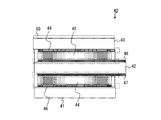
- FIG. 13 is a cross-sectional view showing an example of a liquid crystal optical element 40 according to Example 1 of the present invention.
- the liquid crystal optical element 40 according to the example 1 includes a first substrate 41, a second substrate 42, a third substrate 43, a first liquid crystal layer 44, a second liquid crystal layer 45, a first transparent electrode 46 ( Second transparent electrode), second transparent electrode 47 (first transparent electrode), third transparent electrode 48 (first transparent electrode), fourth transparent electrode 49 (second transparent electrode), 1 / 4 wavelength plate 50 and the like.
- an optical path until a light beam emitted from a laser light source (light source) is collected on an information recording layer of an optical disk by an objective optical element is referred to as a first optical path.
- the optical path until the light beam reflected by the information recording layer of the optical disc is detected by the photodetector is referred to as a second optical path.
- the first liquid crystal layer 44 is sandwiched between the first substrate 41 and the second substrate 42. Specifically, the first liquid crystal layer 44 is formed by sealing liquid crystal in a space formed by a first substrate 41, a second substrate 42, and a seal as a spacer.
- the second liquid crystal layer 45 is sandwiched between the second substrate 42 and the third substrate 43. Specifically, the second liquid crystal layer 45 is formed by sealing liquid crystal in a space formed by the second substrate 42, the third substrate 43, and a seal.
- the alignment direction of the first liquid crystal layer 44 and the alignment direction of the second liquid crystal layer 45 are orthogonal to each other.
- a polarization beam splitter is disposed between a laser light source and an objective optical element.
- the first optical path and the second optical path can be partially overlapped, and the optical system can be made small.
- the polarization direction of the light beam rotates 90 degrees when reflected by the optical disc. That is, the polarization direction of the incident light (the light beam in the first optical path) and the polarization direction of the reflected light (the light beam in the second optical path) are orthogonal to each other.
- the polarizing beam splitter transmits the light beam emitted from the laser light source and makes it incident on the objective optical element.
- the polarization beam splitter reflects the light beam reflected from the optical disk and transmitted through the objective optical element, and guides it to the photodetector.
- the liquid crystal optical element 40 according to the first embodiment includes the first liquid crystal layer 44 and the second liquid crystal layer 45, and the alignment direction of the first liquid crystal layer 44 and the alignment direction of the second liquid crystal layer 45 are mutually different. Since they are orthogonal, it is possible to correct both incident light and reflected light.
- the alignment direction of the first liquid crystal layer 44 is an alignment direction that acts on incident light.
- the alignment direction of the second liquid crystal layer 45 is an alignment direction that acts on the reflected light.
- the first transparent electrode 46 is formed on the first liquid crystal layer 44 side of the first substrate 41.
- the fourth transparent electrode 49 is formed on the second liquid crystal layer 45 side of the third substrate 43.
- the electrode pattern of the 1st transparent electrode 46 and the 4th transparent electrode 49 has an electrode pattern for performing compatibility between each information recording layer of multilayer BD74.
- the electrode patterns of the first transparent electrode 46 and the fourth transparent electrode 49 are substantially the same as the electrode patterns of the upper transparent electrode 14 and the lower transparent electrode 15 of the liquid crystal optical element 10. That is, the first transparent electrode 46 and the fourth transparent electrode 49 have a pattern in which a plurality of nine transparent electrodes formed in a circular shape having different sizes are arranged concentrically. Further, the first liquid crystal layer 44 and the second liquid crystal layer 45 are divided into nine regions (second regions) by the plurality of transparent electrodes. Then, each region of the first liquid crystal layer 44 and the second liquid crystal layer 45 generates a phase difference of OL0, OL1, OL2, OL3, OL4 in the light beam transmitted through the region.
- spherical aberration based on the difference in the cover layer thickness of each information recording layer of the two-layer BD is corrected by generating five kinds of phase differences OL0 to OL4 in the light beam transmitted through the liquid crystal optical element 40. .
- the second transparent electrode 47 is formed on the first liquid crystal layer 44 side of the second substrate 42.
- the third transparent electrode 48 is formed on the second liquid crystal layer 45 side of the second substrate 42.
- the electrode pattern of the 2nd transparent electrode 47 and the 3rd transparent electrode 48 is an electrode pattern which correct
- the second transparent electrode 47 and the third transparent electrode 48 have a predetermined cover layer thickness of the optical disc on which the objective lens provided on the optical disc side of the liquid crystal optical element 10 condenses the light beam, and BD
- the electrode pattern corrects spherical aberration based on the cover layer thickness difference between the HD and the cover layer.
- the second transparent electrode 47 and the third transparent electrode 48 have a pattern in which a plurality of transparent electrodes formed in circular shapes having different sizes are arranged concentrically.
- the first liquid crystal layer 44 and the second liquid crystal layer 45 are divided into a plurality of regions (first regions) by the plurality of transparent electrodes. Then, each region of the first liquid crystal layer 44 and the second liquid crystal layer 45 corrects the spherical aberration based on the cover layer thickness difference between the cover layer thickness and the BD or HD in the light beam transmitted through the region. A phase difference is generated.
- the plurality of regions divided by the second transparent electrode 47 and the third transparent electrode 48 are substantially (m / m) in the luminous flux transmitted through the liquid crystal optical element 40 within the range of the numerical aperture of HD.
- n is a natural number satisfying n ⁇ 2
- m is an integer satisfying
- ⁇ is the wavelength of the light source
- the first liquid crystal layer 44 is driven by the first transparent electrode 46 and the second transparent electrode 47.
- the first liquid crystal layer 44 has a phase difference that reduces spherical aberration based on the cover layer thickness difference between the information recording layers of the multilayer BD 74 with respect to the incident light. generate.
- an objective optical element 104 (described later) is defocused by an actuator 106 described later, the first liquid crystal layer 44 driven by the first transparent electrode 46 has a multi-layer HD 72 for the incident light.
- a phase difference that reduces spherical aberration based on the difference in cover layer thickness between the information recording layers is generated.
- the first liquid crystal layer 44 when the first liquid crystal layer 44 is driven by the second transparent electrode 47, the first liquid crystal layer 44 generates a phase difference that reduces spherical aberration based on the cover layer thickness difference between BD and HD with respect to incident light.
- the second liquid crystal layer 45 is driven by the third transparent electrode 48 and the fourth transparent electrode 49. Then, when driven by the third transparent electrode 48, the second liquid crystal layer 45 generates a phase difference that reduces spherical aberration based on the cover layer thickness difference between BD and HD with respect to the reflected light.
- the second liquid crystal layer 45 when driven by the fourth transparent electrode 49, the second liquid crystal layer 45 reduces the spherical aberration based on the cover layer thickness difference between the information recording layers of the multilayer BD 74 with respect to the reflected light. Generate a phase difference.
- the objective optical element 104 (described later) is defocused, the second liquid crystal layer 45 driven by the fourth transparent electrode 49 is provided between the information recording layers of the multilayer HD 72 with respect to the reflected light. A phase difference that reduces spherical aberration based on the cover layer thickness difference is generated.
- the quarter-wave plate 50 is fixed to the surface of the third substrate 43 on the objective lens 105 (described later) side.
- the first substrate 41 side of the liquid crystal optical element 40 is a laser light source 101 (described later) side
- the third substrate 43 side of the liquid crystal optical element 40 is an optical disc 75 (described later) side.
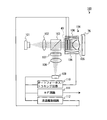
- FIG. 14 shows an example of the optical head device 100 according to the first embodiment.
- the optical head device 100 includes a laser light source 101, a collimator lens 102, a polarizing beam splitter 103, an objective optical element 104, an actuator 106, a hologram optical element 107, a detection condensing lens 108, and a photodetector 109.
- the objective optical element 104 includes a liquid crystal optical element 40, an objective lens 105, and the like. Further, the liquid crystal optical element 40 and the objective lens 105 are integrally held by an actuator 106. The liquid crystal optical element 40 and the objective lens 105 are integrally driven by the actuator 106.
- the actuator 106 includes a mechanism for driving the objective optical element 104 at high speed and with high accuracy.
- the actuator 106 moves the objective optical element 104 along two axes, ie, the optical axis direction of the objective lens 105 and a direction perpendicular to the optical axis direction. As a result, the actuator 106 defocuses the objective optical element 104.
- the actuator 106 controls the position of the light spot formed by the objective lens 105 on the optical disc 75.
- the light beam (incident light) emitted from the laser light source 101 passes through the collimator lens 102, the polarization beam splitter 103, the liquid crystal optical element 40, and the objective lens 105 and enters the optical disc 75.
- the light beam (reflected light) reflected from the optical disk 75 passes through the objective lens 105 and the liquid crystal optical element 40 and then enters the hologram optical element 107.
- the hologram optical element 107 separates the reflected light reflected from the optical disk 75 into an autofocus / tracking servo component and an RF component.
- the reflected light that has passed through the hologram optical element 107 is condensed by the detection condenser lens 108, detected by the photodetector 109, and converted into an electrical signal.
- the autofocus / tracking component signal detected by the photodetector 109 is input to the autofocus / tracking circuit 110.
- the autofocus / tracking circuit 110 outputs a control signal based on the autofocus / tracking component signal. Based on the control signal output from the autofocus / tracking circuit 110, the actuator 106 is controlled.
- the RF component signal detected by the photodetector 109 is input to the RF circuit 111.
- the RF circuit 111 outputs an RF signal based on the RF component signal.
- the liquid crystal driving circuit 112 inputs a driving signal to the first transparent electrode 46, the second transparent electrode 47, the third transparent electrode 48, and the fourth transparent electrode 49. Then, the liquid crystal driving circuit 112 has a first transparent electrode 46, a second transparent electrode 47, and a third transparent electrode 48 when the operating environment of the first liquid crystal layer 44 and the second liquid crystal layer 45 changes. The amount of voltage applied to the fourth transparent electrode 49 is adjusted.
- the first transparent electrode 46, the second transparent electrode 47, the third The amount of voltage applied to the transparent electrode 48 and the fourth transparent electrode 49 is adjusted. Such adjustment may be performed only at the start of the operation of the first liquid crystal layer 44 and the second liquid crystal layer 45, or may be performed during the operation.
- the surface of the objective lens 105 on the liquid crystal optical element 40 side is divided into a central portion and an outer peripheral portion.
- the outer peripheral portion is a ring-shaped region provided on the outer peripheral side of the central portion.
- the outer peripheral portion has a surface shape that favorably collects a light beam with respect to a BD having a cover layer thickness of 0.1 mm.
- BD and HD differ not only in cover layer thickness but also in NA. Therefore, just because the central portion of the objective lens 105 has a surface shape that reduces spherical aberration when converging the light beam on the optical disc having a cover layer thickness intermediate between BD and HD, Are not necessarily equal in absolute value of spherical aberration when condensing light on BD or HD.
- the correction amount by the liquid crystal optical element 40 can be controlled by adjusting the voltage applied to each of the transparent electrodes 46 to 49. Therefore, even if the absolute values of the spherical aberration in BD and the spherical aberration in HD are not equal, the spherical aberration can be suitably reduced.
- the light flux was condensed on the two-layer BD and the two-layer HD.
- a light spot was formed in each information recording layer of the two-layer BD without driving the liquid crystal optical element 40.
- the information recording layer having the larger spherical aberration that is, the disturbance of the light spot is large
- the light beam was condensed on the information recording layer on the objective lens 105 side (that is, the information recording layer on the cover layer side).
- the RMS wavefront aberration was about 200 m ⁇ at the maximum.
- the RMS wavefront aberration could be reduced to 30 m ⁇ . That is, by driving the liquid crystal optical element 40, the wavefront aberration could be reduced to 1 ⁇ 4 or less of that before driving.
- a light spot was formed on each information recording layer of the two-layer HD without driving the liquid crystal optical element 40.
- the information recording layer with the larger spherical aberration was focused.
- the light beam was condensed on the information recording layer on the objective lens 105 side.
- the RMS wavefront aberration was about 100 m ⁇ at the maximum.
- the RMS wavefront aberration could be reduced to 35 m ⁇ . That is, by driving the liquid crystal optical element 40, the wavefront aberration could be reduced to 1 ⁇ 4 or less of that before driving.
- the aberration correction amount by the liquid crystal optical element 40 can be increased by increasing the thickness of the liquid crystal layer or increasing the magnitude of the applied voltage. Moreover, the accuracy of correction can be improved by making the electrode pattern of the transparent electrode finer. For example, by driving the liquid crystal optical element 40, a wavefront aberration amount of 0.2 ⁇ or less can be obtained. In addition, by changing the phase amount to be corrected according to the cover layer thickness error, it is possible to perform compatibility between information recording layers in a multilayer optical disc having a larger number of layers than two layers.
- FIG. 15 is a cross-sectional view showing an example of a liquid crystal lens 60 according to Example 2 of the present invention.
- the liquid crystal lens 60 according to the second example includes a first substrate 61, a second substrate 62, a third substrate 63, a first liquid crystal layer 64, a second liquid crystal layer 65, and first transparent electrodes 66 and 66. , Second transparent electrodes 67, 67, a quarter-wave plate 51, and the like.
- the first liquid crystal layer 64 is sandwiched between the first substrate 61 and the second substrate 62.
- the second liquid crystal layer 65 is sandwiched between the second substrate 62 and the third substrate 63. Further, the alignment direction of the first liquid crystal layer 64 and the alignment direction of the second liquid crystal layer 65 are perpendicular to each other.
- the alignment direction of the first liquid crystal layer 64 is an alignment direction that acts on the reflected light.
- the alignment direction of the second liquid crystal layer 65 is an alignment direction that acts on incident light.
- the first transparent electrodes 66 and 66 are formed on the first liquid crystal layer 64 side and the second liquid crystal layer 65 side of the second substrate 62.
- the second transparent electrodes 67 and 67 are formed on the first liquid crystal layer 64 side of the first substrate 61 and the second liquid crystal layer 65 side of the third substrate 63.
- a blaze grating 68 is formed on the first liquid crystal layer 64 side of the first substrate 61. Similarly, a blaze grating 68 is formed on the second liquid crystal layer 65 side of the second substrate 62.
- the blazed grating 68 acts on the light beam transmitted through the first liquid crystal layer 64, and the BD
- the luminous flux is emitted at a divergence angle that reduces spherical aberration based on the difference in cover layer thickness between HD and HD.
- the liquid crystal element of the first liquid crystal layer 64 is aligned.
- the refractive index of the first liquid crystal layer 64 changes.
- the blaze grating 68 acts on the light beam that passes through the first liquid crystal layer 64.
- the blazed grating 68 acts on the light beam transmitted through the second liquid crystal layer 65, and The luminous flux is emitted at a divergence angle that reduces spherical aberration based on the cover layer thickness difference between BD and HD.
- the quarter wavelength plate 51 is fixed to the surface of the third substrate 63 on the objective lens 205 (described later) side.
- the first substrate 61 side of the liquid crystal lens 60 is the laser light source 101 side
- the third substrate 63 side of the liquid crystal lens 60 is the optical disc 75 side.
- FIG. 16 is a cross-sectional view showing an example of a liquid crystal optical element 70 according to Example 2 of the present invention.
- a liquid crystal optical element 70 according to Example 2 includes a first substrate 71, a second substrate 72, a third substrate 73, a first liquid crystal layer 74, a second liquid crystal layer 75, a first transparent electrode 76, A second transparent electrode 77 and the like are provided.
- the first liquid crystal layer 74 is sandwiched between the first substrate 71 and the second substrate 72.
- the second liquid crystal layer 75 is sandwiched between the second substrate 72 and the third substrate 73. Further, the alignment direction of the first liquid crystal layer 74 and the alignment direction of the second liquid crystal layer 75 are perpendicular to each other.
- the alignment direction of the first liquid crystal layer 74 is an alignment direction that acts on incident light.
- the alignment direction of the second liquid crystal layer 75 is an alignment direction that acts on the reflected light.
- the first transparent electrode 76 is formed on the first liquid crystal layer 74 side of the second substrate 72.
- the second transparent electrode 77 is formed on the second liquid crystal layer 75 side of the second substrate 72.
- the electrode pattern of the 1st transparent electrode 76 and the 2nd transparent electrode 77 has an electrode pattern for performing compatibility between each information recording layer of multilayer BD74.
- the electrode patterns of the first transparent electrode 76 and the second transparent electrode 77 are the same as the electrode patterns of the first transparent electrode 46 and the fourth transparent electrode 49 of the liquid crystal optical element 40 according to the first embodiment. It is almost the same.
- the first liquid crystal layer 74 when driven by the first transparent electrode 76, the first liquid crystal layer 74 reduces the spherical aberration based on the cover layer thickness difference between the information recording layers of the multilayer BD 74 with respect to the incident light. Generate a phase difference. Further, when an objective optical element 204 (described later) is defocused by an actuator 206 described later, the first liquid crystal layer 74 driven by the first transparent electrode 76 has a multi-layer HD 72 with respect to incident light. A phase difference that reduces spherical aberration based on the difference in cover layer thickness between the information recording layers is generated.
- the second liquid crystal layer 75 when driven by the second transparent electrode 77, the second liquid crystal layer 75 reduces the spherical aberration based on the cover layer thickness difference between the information recording layers of the multilayer BD 74 with respect to the reflected light. Generate a phase difference.
- the objective optical element 204 (described later) is defocused, the second liquid crystal layer 75 driven by the second transparent electrode 77 is reflected between the information recording layers of the multilayer HD 72 with respect to the reflected light. A phase difference that reduces spherical aberration based on the cover layer thickness difference is generated.
- the first transparent electrode 76 and the second transparent electrode 77 are formed on the same substrate (second substrate 72). Therefore, the alignment accuracy of the first transparent electrode 76 and the second transparent electrode 77 is increased.
- Example 2 the first substrate 71 side of the liquid crystal optical element 70 is the laser light source 101 side, and the third substrate 73 side of the liquid crystal optical element 70 is the optical disc 75 side.
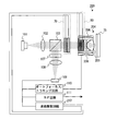
- FIG. 17 shows an example of an optical head device 200 according to the second embodiment.
- the optical head device 200 according to the second embodiment is different from the optical head device 100 according to the first embodiment only in the configuration of the liquid crystal optical element 70, the objective optical element 204, the actuator 206, and the liquid crystal driving circuit 212. Since they are different, the same components are denoted by the same reference numerals and description thereof is omitted.
- the objective optical element 204 includes a liquid crystal lens 60, an objective lens 205, and the like. Further, the liquid crystal lens 60 and the objective lens 205 are integrally held by an actuator 206. The liquid crystal lens 60 and the objective lens 205 are integrally driven by an actuator 206.
- the actuator 206 includes a mechanism for driving the objective optical element 204 at high speed and with high accuracy.
- the actuator 206 moves the objective optical element 204 along two axes, ie, the optical axis direction of the objective lens 205 and a direction perpendicular to the optical axis direction. As a result, the actuator 206 defocuses the objective optical element 204.
- the actuator 206 controls the position of the light spot formed by the objective lens 205 on the optical disk 75.
- the liquid crystal drive circuit 212 sends drive signals to the first transparent electrodes 66 and 66, the second transparent electrodes 67 and 67 of the liquid crystal lens 60, the first transparent electrode 76 and the second transparent electrode 77 of the liquid crystal optical element 70. input. Then, the liquid crystal driving circuit 212 changes the first transparent electrodes 66 and 66 and the second transparent electrodes of the liquid crystal lens 60 when the operating environment of the first liquid crystal layer 64 and the second liquid crystal layer 65 of the liquid crystal lens 60 changes. The amount of voltage applied to the transparent electrodes 67 and 67 is adjusted.
- the liquid crystal driving circuit 212 has the first transparent electrode 76 and the second transparent electrode 76 of the liquid crystal optical element 70 when the operating environment of the first liquid crystal layer 74 and the second liquid crystal layer 75 of the liquid crystal optical element 70 changes. The amount of voltage applied to the transparent electrode 77 is adjusted.
- the objective lens 205 is a BD dedicated lens.
- the objective lens 205 converges the light beam well on the information recording layer of the BD.
- the liquid crystal optical element 70 is provided between the objective optical element 204 and the polarization beam splitter 103. If the liquid crystal optical element 70 is also mounted on the actuator 206, the influence when a lens shift occurs can be reduced. However, if many actuators are mounted, problems arise in signal quality and high-speed operation. Further, the amount of aberration to be corrected by the liquid crystal optical element 70 is smaller than that of the liquid crystal lens 60. Therefore, the amount of coma caused by lens shift is small. It is also possible to correct the coma caused by the lens shift by the liquid crystal optical element 70.
- FIG. 18 is a cross-sectional view of the objective optical element 204 and the optical disc 75.
- the optical disc 75 a single layer HD 71 and a single layer BD 73 are exemplified.
- FIG. 18A shows a case where a light spot is formed on the single layer HD 71
- FIG. 18B shows a case where a light spot is formed on the single layer BD 73.
- the liquid crystal lens 60 is driven.
- the blazed grating 68 acts on the light beam that passes through the second liquid crystal layer 65 of the liquid crystal lens 60.
- the liquid crystal lens 60 adjusts the divergence angle of the light beam so that the light beam transmitted through the liquid crystal lens 60 is condensed on the single layer HD 71 by the NA of HD.
- the light beam transmitted through the second liquid crystal layer 65 diverges at a divergence angle that reduces spherical aberration based on the cover layer thickness difference between the single layer BD 73 and the single layer HD 71 and enters the objective lens 205. Therefore, the objective lens 205 condenses the light beam emitted from the liquid crystal lens 60 on the single layer HD 71 satisfactorily.
- the liquid crystal lens 60 is not driven. Therefore, the light beam passing through the liquid crystal lens 60 enters the objective lens 205 without changing the divergence angle. Therefore, since the objective lens 205 is a BD-dedicated lens, the light beam emitted from the liquid crystal lens 60 is favorably condensed on the single layer BD73.
- the light flux was condensed on the two-layer BD and the two-layer HD.
- a light spot was formed on each information recording layer of the two-layer BD without driving the liquid crystal optical element 70.
- the information recording layer having the larger spherical aberration that is, the disturbance of the light spot is large
- the light beam was condensed on the information recording layer on the objective lens 205 side (that is, the information recording layer on the cover layer side).
- the liquid crystal optical element 70 was not driven, the RMS wavefront aberration was about 180 m ⁇ at the maximum.
- the RMS wavefront aberration could be reduced to 25 m ⁇ . That is, by driving the liquid crystal optical element 70, the wavefront aberration could be reduced to 1 ⁇ 4 or less of that before driving.
- the liquid crystal lens 60 and not driving the liquid crystal optical element 70 a light spot was formed on each information recording layer of the two-layer HD.
- the information recording layer with the larger spherical aberration was focused.
- the light beam was condensed on the information recording layer on the objective lens 205 side.
- the RMS wavefront aberration was about 140 m ⁇ at the maximum.
- the RMS wavefront aberration could be reduced to 30 m ⁇ by driving not only the liquid crystal lens 60 but also the liquid crystal optical element 70. That is, by driving the liquid crystal optical element 70, the wavefront aberration could be reduced to 1 ⁇ 4 or less of that before driving.
- the blazed grating 68 is provided on the liquid crystal lens 60, but the liquid crystal lens 60 may be formed by other configurations. For example, by arranging a plurality of transparent electrodes formed in circular shapes of different sizes in a concentric manner, dividing the liquid crystal layer into a plurality of annular zones, and changing the refractive index of the liquid crystal layer in each region stepwise
- the liquid crystal lens 60 may be configured. However, in this case, the lead lines of the transparent electrode increase.
- FIG. 19 shows an optical head device 300 according to the third embodiment.
- the optical head device 300 according to the third embodiment includes a liquid crystal optical element 80, an objective optical element 304, a BD / HD optical path switching mechanism 306 (optical path switching mechanism), an actuator 307, and a liquid crystal driving circuit 312. Only the optical head device 100 according to the first embodiment is different from the optical head device 100 according to the first embodiment.
- the liquid crystal optical element 80 is obtained by providing a quarter wavelength plate 52 on the optical disc side of the liquid crystal optical element 70 according to the second embodiment.
- the light flux transmitted through the liquid crystal optical element 80 has a phase difference that reduces spherical aberration based on the cover layer thickness difference between the information recording layers in the multilayer BD and the multilayer HD. generate.
- the objective optical element 304 includes a first objective lens 308, a second objective lens 309, and the like.
- the first objective lens 308 and the second objective lens 309 are arranged in a direction perpendicular to the optical axis direction of the lens.
- the first objective lens 308 and the second objective lens 309 are integrally held by an actuator 307.
- the first objective lens 308 is a BD dedicated lens.
- the second objective lens 309 is an HD-only lens.
- the BD / HD optical path switching mechanism 306 includes a liquid crystal optical path switching element (not shown).
- the liquid crystal optical path switching element selects either an optical path toward the first objective lens 308 or an optical path toward the second objective lens 309 using polarized light.
- the BD / HD optical path switching mechanism 306 may select an optical path by driving a mirror.
- the actuator 307 has a mechanism for driving the objective optical element 304 at high speed and with high accuracy.
- the actuator 307 moves the objective optical element 304 along two axes, ie, the optical axis direction of the first objective lens 308 and the second objective lens 309 and a direction perpendicular to the optical axis direction. . Thereby, the actuator 307 defocuses the objective optical element 304.
- the actuator 307 controls the position on the BD 73 (74) of the light spot formed by the first objective lens 308. Similarly, the actuator 307 controls the position of the light spot formed by the second objective lens 309 on the HD 71 (72).
- the liquid crystal drive circuit 312 inputs a drive signal to the liquid crystal optical element 80.
- the liquid crystal driving circuit 312 adjusts the amount of voltage applied to the transparent electrode of the liquid crystal optical element 80 when the operating environment of the liquid crystal layer of the liquid crystal optical element 80 changes.
- the light flux was focused on the two-layer BD74 and the two-layer HD72.
- a light spot was formed in each information recording layer of the two-layer BD 74 without driving the liquid crystal optical element 80.
- the information recording layer having the larger spherical aberration that is, the disturbance of the light spot is large
- the light beam was condensed on the information recording layer on the first objective lens 308 side (that is, the information recording layer on the cover layer side).
- the liquid crystal optical element 80 was not driven, the RMS wavefront aberration was about 160 m ⁇ at the maximum.
- the RMS wavefront aberration could be reduced to 25 m ⁇ . That is, by driving the liquid crystal optical element 80, the wavefront aberration could be reduced to 1 ⁇ 4 or less of that before driving.
- a light spot was formed on each information recording layer of the two-layer HD 72 without driving the liquid crystal optical element 80.
- the information recording layer having the larger spherical aberration was focused.
- the light beam was condensed on the information recording layer on the second objective lens 309 side in the information recording layer of the two-layer HD 72.
- the liquid crystal optical element 80 was not driven, the RMS wavefront aberration was about 90 m ⁇ at the maximum.
- the RMS wavefront aberration could be reduced to 20 m ⁇ . That is, by driving the liquid crystal optical element 80, the wavefront aberration could be reduced to 1 ⁇ 4 or less of that before driving.
- the BD / HD optical path switching mechanism 306 is required. Further, since two lenses are used, the lens weight and size increase, and the burden on the actuator increases. In addition, since two lenses are used, the signal is significantly deteriorated when a lens shift occurs. However, since the first objective lens 308, which is a BD-dedicated lens, and the second objective lens, which is an HD-dedicated lens, are used, wavefront aberration can be further reduced. Specifically, the occurrence of spherical aberration based on the cover layer thickness difference between BD73 (74) and HD71 (72) is prevented.
- the present invention describes a method for reducing spherical aberration, and it is possible to reduce both spherical aberration based on the cover layer thickness difference of each information recording layer in a multilayer optical disc and minute spherical aberration based on defocus.
- the two-layer BD and the two-layer HD are exemplified as two types of multilayer optical disks, but the scope of the present invention is not limited to this.
- the present invention is also applicable to DVDs and CDs.
- spherical aberration based on the cover layer thickness difference of each information recording layer of DVD or CD occurs at the wavelength of the light source used in the optical system. Therefore, the defocus amount and the voltage amount applied to the transparent electrode of the liquid crystal optical element are adjusted according to the spherical aberration amount. This makes it possible to reduce not only BD and HD but also spherical aberration of DVD or CD.
- Liquid crystal optical element 13 Liquid crystal layer (liquid crystal layer of liquid crystal optical element) 14 Top transparent electrode (transparent electrode) 15 Bottom transparent electrode (transparent electrode) 44, 45 First liquid crystal layer (liquid crystal layer of liquid crystal optical element) 46 1st transparent electrode (2nd transparent electrode) 47 Second transparent electrode (first transparent electrode) 48 Third transparent electrode (first transparent electrode) 49 Fourth transparent electrode (second transparent electrode) 60 Liquid crystal lens 64, 65 Liquid crystal layer (Liquid crystal layer of liquid crystal lens) 68 Blaze grating 71 Single layer HD (second optical disk) 72 multilayer HD (second multilayer optical disc) 73 Single layer BD (first optical disc) 74 Multilayer BD (first multilayer optical disc) 74, 75 Second liquid crystal layer (liquid crystal layer of liquid crystal optical element) 76 1st transparent electrode (2nd transparent electrode) 77 Second transparent electrode (second transparent electrode) 100, 200, 300 Optical head device 90, 104, 204, 304 Objective optical element 105, 205 Objective lens 306 BD
Landscapes
- Physics & Mathematics (AREA)
- Optics & Photonics (AREA)
- Optical Head (AREA)
Abstract
液晶光学素子10は、同心円状に並べられた大きさの異なる円形状の複数の透明電極により複数の領域に分割された液晶層13を備え、複数の透明電極は、多層BDの各情報記録層のカバー層厚差に基づく球面収差を低減するような電極パターンで形成されている。そして、対物光学素子をデフォーカスし、複数の領域が液晶光学素子10を透過する光束に付与する位相差が、液晶光学素子10の中心から外周に向かって小さくなるように、複数の透明電極に電圧が印加された場合に、複数の領域は、液晶光学素子10を透過する光束に、多層HDの各情報記録層のカバー層厚差に基づく球面収差を低減するような位相差を付与する。
Description
本発明は、液晶光学素子の駆動方法、光ヘッド装置、及び、液晶光学素子に関し、特に、1種類の波長の光束を複数種類の光ディスクに集光させる場合に、光ディスクの記録層までのカバー層の厚みと対物レンズの対応カバー層厚とのズレに基づく収差補正を行う液晶光学素子の駆動方法、光ヘッド装置、及び、液晶光学素子に関する。
従来、CD(Compact Disc)、DVD(Digital Versatile Disc)、MO(Magnetic Optical Disk)などの光ディスク(光記録媒体)に光学的に情報を記録し、当該光ディスクに記録された情報を再生する光ディスク装置(光情報記録再生装置)が開発されている。また、最近では、HD(High Definition DVD)やBD(Blu-ray Disc)などの大容量の高密度光ディスクも開発されている。これらの光ディスクは、情報記録層の光が入射する側がカバー層に覆われた構造を有する。カバー層は、透明樹脂からなる。例えば、DVDの記録/再生において、波長が660nm帯である半導体レーザが光源として用いられる。また、DVDの記録/再生において、NA(開口数)が0.6から0.65である対物レンズが用いられる。現在、光ディスク1枚当たりに所定の記録容量のデータを記録させるために、情報記録層に、必要な大きさの記録マークが形成されている。波長の短い光束を出射する光源と、NAの大きい対物レンズを用いることにより、情報記録層にさらに小さな記録マークを形成することができる。そして、波長が405nmである半導体レーザと、NAが0.85である対物レンズとを用いて記録/再生を行うBD規格が提案されている。また、波長が405nmである半導体レーザと、NAが0.65である対物レンズとを用いて記録/再生を行うHD規格が提案されている。BDのカバー層の厚さは0.1mmであり、HDのカバー層の厚さは0.6mmである。そのため、BDとHDのカバー層厚は異なる。
そのため、1台の光ディスク装置によりBDとHDの両方の光ディスクを記録/再生する場合、BDとHDのカバー層厚の違いに基づく球面収差を補正する必要がある。
そのため、1台の光ディスク装置によりBDとHDの両方の光ディスクを記録/再生する場合、BDとHDのカバー層厚の違いに基づく球面収差を補正する必要がある。
また、さらに、光ディスクの記録容量を向上するため、情報記録層を複数有する光ディスク(以下、多層光ディスクと称する。)が提案されている。例えば、BD2層規格、HD3層規格などが提案されている。多層光ディスクでは、それぞれの情報記録層までの実施的なカバー層厚は異なる。そのため、多層光ディスクを記録/再生するためには、各情報記録層のカバー層厚に応じて、複数の対応カバー層厚を有するように、光ディスク装置に搭載される対物レンズなどの光学系を構築する必要がある。
従って、現在、カバー層厚の異なる複数種類の光ディスク間の互換を行う互換技術と、多層光ディスクにおける複数の情報記録層間の互換を行う互換技術との両方の互換技術を備えた光ディスク装置の開発が望まれている。
そして、カバー層厚の異なる複数種類の光ディスク間の互換を行う互換技術として、DVDとCDとの互換を行う互換技術が提案されている。例えば、特許文献1に記載の光ディスク装置は、DVD専用レンズとCD専用レンズを回動型の2レンズアクチュエータに搭載している。そして、DVD専用レンズとCD専用レンズとを切り替えることにより、DVDとCDとの互換を行っている。
また、特許文献2に記載の光ディスク装置は、赤色半導体レーザから出射された光束の一部を0次光として透過させ、赤色半導体レーザから出射された光束の一部を1次回折光として透過させるホログラム素子を対物レンズと一体に構成している。そして、ホログラム素子と一体化された対物レンズが0次光をDVDに集光し、ホログラム素子と一体化された対物レンズが1次回折光をCDに集光するように、ホログラム素子の回折パターンを設計している。具体的には、ホログラム素子は、CDとDVDとのカバー層厚差によって生じる球面収差を補正するように、赤色半導体レーザから出射された光束の一部を1次回折光として透過させる。これにより、1つの波長でカバー層厚とNAの異なる2種類の光ディスクの再生互換を実現している。
今日、CD・DVD互換再生用光ピックアップには、赤色半導体レーザと、波長780nmの赤外半導体レーザとが搭載されている。CD-Rでは、赤色半導体レーザ光の反射率が著しく低下して再生することができない。そのため、CDの再生には、赤外半導体レーザが用いられる。そして、CD・DVD互換再生用光ピックアップでは、CDとDVDとでは、再生に用いる光源波長が異なることを利用した互換再生方式が用いられている。しかし、DVD再生用光ピックアップの開発当初では、CD-Rの再生が必須とされていなかったため、赤色半導体レーザのみを用いるDVDとCDの互換再生方式が検討されていた。したがって、DVD再生用光ピックアップの開発当初に検討された赤色半導体レーザのみを用いるDVDとCDの互換再生方式の技術を応用することにより、青色半導体レーザのみを用いるBDとHDの互換再生方式を開発できる可能性がある。
例えば、特許文献3では、CDに集光するために必要なNAの範囲における対物レンズの形状をDVDとCDとの中間のカバー層厚に最適に集光するように形成し、CDに集光するために必要なNAの範囲より外縁側のDVDに集光するために必要なNAの範囲内における対物レンズの形状をDVDに最適に集光するように形成している。これにより、CDとDVDとの互換を図っている。
また、特許文献4では、収差補正用素子として液晶光学素子を用いている。そして、液晶光学素子により、収差補正と光量制御を同時に行っている。
また、特許文献5、6では、収差補正用素子として液晶光学素子を用いている。そして、液晶光学素子により、カバー層厚差に基づく球面収差を低減している。これにより、カバー層厚の異なる複数種類の光ディスク間の互換を図っている。
また、特許文献5、6では、収差補正用素子として液晶光学素子を用いている。そして、液晶光学素子により、カバー層厚差に基づく球面収差を低減している。これにより、カバー層厚の異なる複数種類の光ディスク間の互換を図っている。
また、特許文献7では、赤色半導体レーザ光源とコリメータレンズとの間隔を可変となるように構成している。そして、CDとDVDとで、赤色半導体レーザ光源とコリメータレンズとの間隔を変えることにより、対物レンズに入射する光の発散度合いを変えて、CDとDVDとのカバー層厚の違いによる球面収差を補正している。これにより、CDとDVDとの互換を図っている。
また、特許文献8では、1つのガラス基板に2層以上の透明電極パターンを形成した液晶光学素子が記載されている。
しかしながら、上記従来技術を組み合わせて、BDとHDとの互換を行う互換技術や、多層光ディスクにおける複数の情報記録層間の互換を行う互換技術を構成することは難しい。具体的には、特許文献1乃至3及び特許文献5に記載の何れかの技術と、特許文献4又は特許文献7に記載の技術を組み合わせることにより、BDとHDとの互換を行う互換技術、及び、多層光ディスクにおける複数の情報記録層間の互換を行う互換技術を構成することは可能である。しかし、実用上、大きな問題がある。
例えば、特許文献7に記載の技術では、レーザ光源とコリメータレンズとの間隔を変えるため、コリメータレンズを移動させるビームエキスパンダ(レンズ移動機構)を備える必要がある。ビームエキスパンダはサイズが大きい。また、ビームエキスパンダを使用する場合には、レンズを高い精度で組み合わせなければならない。そのため、特許文献7に記載の技術と特許文献1に記載の技術とを組み合わせると、BD用のレンズ及びHD用のレンズのそれぞれにビームエキスパンダを設ける必要がある。そのため、ビームエキスパンダを2つ設けることとなり、サイズ及びコストの点から現実的ではない。
また、特許文献7に記載の技術と、特許文献2、3、5の何れかに記載の技術とを組み合わせると、既に、組み合わせレンズの使用によりサイズが大きくなってしまっている光ヘッド装置がさらに大きくなってしまう。
また、特許文献7に記載の技術と、特許文献2、3、5の何れかに記載の技術とを組み合わせると、既に、組み合わせレンズの使用によりサイズが大きくなってしまっている光ヘッド装置がさらに大きくなってしまう。
また、特許文献4に記載の技術を用いて、BDとHDとの互換を行う互換技術、及び、多層光ディスクにおける複数の情報記録層間の互換を行う互換技術を構成すると、液晶を駆動する透明電極の本数を多くする必要がある。具体的には、BD用の電極パターンと、HD用の電極パターンの2種類の透明電極が必要となる。そして、2つのガラス基板にそれぞれの電極パターンを形成すると、2つの電極パターンの位置合わせを精度良く行う必要がある。また、駆動する透明電極の本数が増えてしまう。また、1つのガラス基板に、複数層の電極パターンを形成してもよいが、駆動する透明電極の本数が増えてしまうことには変わりがない。
本発明は、このような問題点を解決するためになされたものであり、液晶光学素子の透明電極を増やすことなく、複数種類の多層光ディスクにおける複数の情報記録層間の互換を行うことができる液晶光学素子の駆動方法、光ヘッド装置、及び、液晶光学素子を提供することを目的とする。
本発明にかかる液晶光学素子の駆動方法は、第1のカバー層厚を有する第1の多層光ディスクに光源からの光束を第1の開口数で集光させる光ヘッド装置における液晶光学素子の駆動方法である。前記光ヘッド装置は、前記光源からの光束を前記第1の多層光ディスクに集光させる対物光学素子と、同心円状に並べられた大きさの異なる円形状の複数の透明電極により複数の領域に分割された液晶層を備える液晶光学素子と、前記対物光学素子をデフォーカスさせるアクチュエータと、を備えている。また、前記複数の透明電極は、前記複数の領域が、前記液晶光学素子を透過する光束に、前記第1の多層光ディスクの各情報記録層のカバー層厚差に基づく球面収差を低減するような位相差を付与するような電極パターンで形成されている。そして、本発明にかかる液晶光学素子の駆動方法は、前記アクチュエータにより前記対物光学素子をデフォーカスし、前記複数の領域によって前記液晶光学素子を透過する光束に付与される位相差が、前記液晶光学素子の中心から外周に向かって小さくなるように、前記複数の透明電極に電圧を印加するものである。そして、この場合に、前記複数の領域は、前記液晶光学素子を透過する光束に、前記第1のカバー層厚よりも厚い前記第2のカバー層厚を有し、前記第1の開口数より小さい第2の開口数で前記光源からの光束が集光される第2の多層光ディスクの各情報記録層のカバー層厚差に基づく球面収差を低減するような位相差を付与するものである。
また、本発明にかかる光ヘッド装置は、第1のカバー層厚を有する第1の多層光ディスクに光源からの光束を第1の開口数で集光させる光ヘッド装置である。また、本発明にかかる光ヘッド装置は、前記光源からの光束を前記第1の多層光ディスクに集光させる対物光学素子と、同心円状に並べられた大きさの異なる円形状の複数の透明電極により複数の領域に分割された液晶層を備える液晶光学素子と、前記対物光学素子をデフォーカスさせるアクチュエータと、を備えるものである。また、前記複数の透明電極は、前記複数の領域が、前記液晶光学素子を透過する光束に、前記第1の多層光ディスクの各情報記録層のカバー層厚差に基づく球面収差を低減するような位相差を付与するような電極パターンで形成されている。そして、前記アクチュエータにより前記対物光学素子がデフォーカスされ、前記複数の領域が前記液晶光学素子を透過する光束に付与する位相差が、前記液晶光学素子の中心から外周に向かって小さくなるように、前記複数の透明電極に電圧が印加された場合に、前記複数の領域は、前記液晶光学素子を透過する光束に、前記第1のカバー層厚よりも厚い前記第2のカバー層厚を有し、前記第1の開口数より小さい第2の開口数で前記光源からの光束が集光される第2の多層光ディスクの各情報記録層のカバー層厚差に基づく球面収差を低減するような位相差を付与するものである。
また、本発明にかかる液晶光学素子は、同心円状に並べられた大きさの異なる円形状の複数の透明電極と、前記複数の透明電極により複数の領域に分割された液晶層と、を備える。また、前記複数の透明電極は、前記複数の領域が、前記液晶光学素子を透過する光束に、第1のカバー層厚を有し、第1の開口数で光源からの光束が集光される第1の多層光ディスクの各情報記録層のカバー層厚差に基づく球面収差を低減するような位相差を付与するような電極パターンで形成されている。そして、前記複数の領域が前記液晶光学素子を透過する光束に付与する位相差が、前記液晶光学素子の中心から外周に向かって小さくなるように、前記複数の透明電極に電圧が印加された場合に、前記複数の領域は、前記液晶光学素子を透過する光束に、前記第1のカバー層厚よりも厚い前記第2のカバー層厚を有し、前記第1の開口数より小さい第2の開口数で前記光源からの光束が集光される第2の多層光ディスクの各情報記録層のカバー層厚差に基づく球面収差を低減するような位相差を付与するものである。
本発明においては、第1の多層光ディスクの各情報記録層のカバー層厚差に基づく球面収差を低減するように形成された透明電極を用いて、第2の多層光ディスクの各情報記録層のカバー層厚差に基づく球面収差を低減することができる。これにより、液晶光学素子の透明電極を増やすことなく、複数種類の多層光ディスクにおける複数の情報記録層間の互換を行うことができる。
また、前記液晶光学素子は、複数の第1の透明電極と、複数の第2の透明電極とを備える。また、前記複数の第1の透明電極は、大きさの異なる円形状の複数の透明電極が同心円状に並べられ、前記液晶層を複数の第1の領域に分割する。また、前記複数の第2の透明電極は、大きさの異なる円形状の複数の透明電極が同心円状に並べられ、前記液晶層を複数の第2の領域に分割する。そして、前記複数の第1の領域は、前記液晶光学素子を透過する光束に、前記第1のカバー層厚を有し、前記第1の開口数で前記光源からの光束が集光される第1の光ディスクと、前記第1のカバー層厚よりも厚い前記第2のカバー層厚を有し、前記第1の開口数より小さい第2の開口数で前記光源からの光束が集光される第2の光ディスクとのカバー層厚差に基づく球面収差を低減するような位相差を付与することが好ましい。また、前記複数の第2の領域は、前記液晶光学素子を透過する光束に、前記第1の多層光ディスクの各情報記録層のカバー層厚差に基づく球面収差を低減するような位相差を付与することが好ましい。また、前記複数の第2の領域は、前記アクチュエータにより前記対物光学素子がデフォーカスされ、前記複数の第2の領域が前記液晶光学素子を透過する光束に付与する位相差が、前記液晶光学素子の中心から外周に向かって小さくなるように、前記複数の第2の透明電極に電圧が印加された場合に、前記液晶光学素子を透過する光束に、前記第2の多層光ディスクの各情報記録層のカバー層厚差に基づく球面収差を低減するような位相差を付与することが好ましい。
これにより、カバー層厚差の異なる複数種類の光ディスクの間の互換を行うことができる。
これにより、カバー層厚差の異なる複数種類の光ディスクの間の互換を行うことができる。
また、前記対物光学素子は、前記第1のカバー層厚と前記第2のカバー層厚との間の所定のカバー層厚を有する光ディスクに光束を良好に集光する面形状を有していることが好ましい。また、前記複数の第1の領域は、前記液晶光学素子を透過する光束に、前記所定のカバー層厚と、前記第1のカバー層厚又は前記第2のカバー層厚とのカバー層厚差に基づく球面収差を低減するような位相差を付与することが好ましい。
これにより、対物光学素子が第1のカバー層厚を有する光ディスクに集光させる際に発生する球面収差の符号と、対物光学素子が第2のカバー層厚を有する光ディスクに集光させる際に発生する球面収差の符号とが反対になる。そのため、何れか一方の光ディスクに光束を集光させる際に、当該液晶光学素子により当該光束に付与する位相差を、当該球面収差を低減するために付与すべき位相差から1λずらすことにより、液晶光学素子に印加すべき電圧の幅を狭くすることができる。
これにより、対物光学素子が第1のカバー層厚を有する光ディスクに集光させる際に発生する球面収差の符号と、対物光学素子が第2のカバー層厚を有する光ディスクに集光させる際に発生する球面収差の符号とが反対になる。そのため、何れか一方の光ディスクに光束を集光させる際に、当該液晶光学素子により当該光束に付与する位相差を、当該球面収差を低減するために付与すべき位相差から1λずらすことにより、液晶光学素子に印加すべき電圧の幅を狭くすることができる。
さらに、前記複数の第1の領域は、前記第2の開口数の範囲において、前記液晶光学素子を透過する光束に、略(m/n)λ(ただし、はn≧2を満たす自然数、mは、|m|≦n/2を満たす整数、λは、前記光源の波長)の位相差を付与する。そして、前記複数の第1の領域は、前記第1の光ディスクに前記光源からの光を集光する場合と、前記第2の光ディスクに前記光源からの光を集光する場合とで、前記位相差の符号を変えて、当該位相差を加えることが好ましい。
また、前記液晶光学素子は、アクチュエータにより、前記対物光学素子と一体的に保持されていることが好ましい。
これにより、レンズシフトが発生しても、液晶光学素子に対するレンズシフトの影響を低減することができる。
これにより、レンズシフトが発生しても、液晶光学素子に対するレンズシフトの影響を低減することができる。
さらに、また、前記対物光学素子は、前記第1のカバー層厚を有する第1の光ディスクに前記光源からの光束を前記第1の開口数で良好に集光する対物レンズと、ガラス基板に挟持された液晶層と、液晶層を駆動する透明電極とを備える液晶レンズと、を備える。そして、前記液晶レンズの前記透明電極に電圧が印加された場合に、前記液晶レンズの前記液晶層は、前記液晶レンズを透過した光束が前記対物レンズにより前記第2のカバー層厚を有する第2の光ディスクに前記第2の開口数で集光されるように、前記液晶レンズを透過する光束の発散角度を調整することが好ましい。
また、前記液晶レンズは、前記液晶層を2つ備え、前記液晶レンズの一の前記液晶層の配向方向と他の前記液晶層の配向方向は直交していることが好ましい。
これにより、液晶レンズは、光ディスクに入射する入射光と光ディスクから反射される反射光との両方に対して作用することができる。
これにより、液晶レンズは、光ディスクに入射する入射光と光ディスクから反射される反射光との両方に対して作用することができる。
さらに、前記対物光学素子は、前記第1のカバー層厚を有する第1の光ディスクに前記光源からの光束を前記第1の開口数で良好に集光する第1の対物レンズと、前記第2のカバー層厚を有する第2の光ディスクに前記光源からの光束を前記第2の開口数で良好に集光する第2の対物レンズと、を備える。また、前記液晶光学素子と前記対物光学素子との間に、前記液晶光学素子から出射された光束を前記第1の対物レンズ又は前記第2の対物レンズへと導く光路切替機構を備えることが好ましい。
また、前記液晶光学素子は、前記液晶層を2つ備え、前記液晶光学素子の一の前記液晶層の配向方向と他の前記液晶層の配向方向は直交していることが好ましい。
これにより、液晶光学素子は、光ディスクに入射する入射光と光ディスクから反射される反射光との両方に対して作用することができる。
これにより、液晶光学素子は、光ディスクに入射する入射光と光ディスクから反射される反射光との両方に対して作用することができる。
本発明により、液晶光学素子の透明電極を増やすことなく、複数種類の多層光ディスクにおける複数の情報記録層間の互換を行うことができる。
以下、本発明を適用した具体的な実施の形態について、図面を参照しながら詳細に説明する。なお、本発明は、以下の実施の形態に限定されるものではない。
まず、本発明の実施の形態では、光学性能を示す指標として、RMS(root mean square)波面収差を用いる。ここで、波面収差とは、レンズを透過した光束の波面形状の、理想的なレンズを透過した光束の波面形状からの偏差である。そして、この偏差を標準偏差で表したものをRMS波面収差という。
まず、本発明の実施の形態では、光学性能を示す指標として、RMS(root mean square)波面収差を用いる。ここで、波面収差とは、レンズを透過した光束の波面形状の、理想的なレンズを透過した光束の波面形状からの偏差である。そして、この偏差を標準偏差で表したものをRMS波面収差という。
また、Max Born, Emil Wolf、草川 徹、"Prinsiples of Optics"、第7版、東海大学出版会、p.686に示されるように、射出瞳上で波面収差がλ/14を超えなければ、像があまり劣化しない(Reileighの4分の1波長則)。像の強度分布は、波面収差の最大値だけでなく、様々な波面の形(収差のタイプ)に適応する。そのため、この法則を用いる場合には、回折焦点における強度の値を指定して、許容条件を決定する必要がある。そこで、Marechal条件というものが考案された。Marechal条件とは、「回折焦点Fにおいて正規化された強度が0.8以上の場合、系は十分に補正されている」というものである。これは、「波面と回折焦点に中心を有する参照球面とのズレの標準偏差(RMS波面収差)がλ/14以下となること」と等価である。
従って、光ヘッド装置を開発する場合には、光ヘッド装置全体においてMarechal条件を満たすように設計する必要がある。また、製造コスト、制御性等の他に、Marechal条件を考慮して、液晶光学素子の領域分割数を設計する必要がある。
図1の上側に、本発明の実施の形態にかかる液晶光学素子10を模式的に示す断面図を示す。また、図1の下側に、液晶光学素子10の電極配置を示す平面図を示す。
図1に示すように、液晶光学素子10は、第1の基板11、第2の基板12、液晶層13、上面透明電極14、下面透明電極15等を備えている。
図1に示すように、液晶光学素子10は、第1の基板11、第2の基板12、液晶層13、上面透明電極14、下面透明電極15等を備えている。
液晶層13は、第1の基板11と第2の基板12との間に挟持されている。具体的には、液晶層13は、液晶が、第1の基板11、第2の基板12、及び、スペーサとしてのシールにより形成される空間に封入されてなる。
上面透明電極14は、第1の基板11の液晶層側の面上に形成されている。また、下面透明電極15は、第2の基板12の液晶層側の面上に形成されている。従って、液晶層13は、上面透明電極14と下面透明電極15とにより挟まれている。
上面透明電極14の電極パターンと下面透明電極15の電極パターンは同じである。また、上面透明電極14及び下面透明電極15の電極パターンは、2層BD(第1の多層光ディスク)の球面収差を補正するための電極パターンである。具体的には、図1に示すように、上面透明電極14及び下面透明電極15の電極パターンは、複数の大きさの異なる円形状に形成された透明電極が同心円状に並べられたパターンとなっている。
円形状の各透明電極には、異なる電圧が印加される。そのため、各透明電極により駆動される液晶の配向方向は異なる。従って、各透明電極により駆動された液晶層13を透過する光束に発生する位相差も異なる。
円形状の各透明電極には、異なる電圧が印加される。そのため、各透明電極により駆動される液晶の配向方向は異なる。従って、各透明電極により駆動された液晶層13を透過する光束に発生する位相差も異なる。
具体的には、図1に示すように、液晶層13の両面には、9本の大きさの異なる円形状に形成された透明電極が同心円状に並べられている。そして、当該9本の透明電極により、液晶層13は、9個の領域に分割されている。一番内側の領域は円形の領域となっている。また、その他の8個の領域は、輪帯状となっている。そして、透明電極によって駆動されることにより、1番内側の領域と1番外側の領域の液晶層13は、当該領域を透過する光束に、OL0という位相差を発生させる。また、透明電極によって駆動されることにより、中心から2番目の領域と6番目の領域の液晶層13は、当該領域を透過する光束に、OL1という位相差を発生させる。また、透明電極によって駆動されることにより、中心から3番目の領域と7番目の領域の液晶層13は、当該領域を透過する光束に、OL2という位相差を発生させる。また、透明電極によって駆動されることにより、中心から4番目の領域と8番目の領域の液晶層13は、当該領域を透過する光束に、OL3という位相差を発生させる。また、透明電極によって駆動されることにより、中心から5番目の領域の液晶層13は、当該領域を透過する光束に、OL4という位相差を発生させる。そして、液晶光学素子10を透過する光束に、OL0~OL4の5種類の位相差を発生させることにより、液晶光学素子10は、2層BDの各情報記録層のカバー層厚の違いに基づく球面収差を補正している。
また、透明電極は、一般的な蒸着法、スパッタリング法などにより、第1の基板11及び第2の基板12上に形成される。具体的には、まず、第1の基板11及び第2の基板12上に、インジウムスズ酸化物(ITO)などの透明電極膜を成膜する。次に、当該透明電極膜をフォトリソ・エッチング法などにより、所望のパターンにエッチングする。なお、透明電極膜材料としては、亜鉛スズ酸化物(ZnO)等の他の材料が用いられてもよい。
図2の真ん中に、比較例1にかかる液晶光学素子20を模式的に示す断面図を示す。また、図2の上側に、液晶光学素子20の上面透明電極24の電極配置を示す平面図を示し、図2の下側に、液晶光学素子20の下面透明電極25の電極配置を示す平面図を示す。なお、比較例1にかかる液晶光学素子20は、従来技術を適用して、BDとHDとの互換と、多層BDの各情報記録層間の互換及び多層HDの各情報記録層間の互換とを行う液晶光学素子として想定されるものである。
図2に示すように、比較例1にかかる液晶光学素子20は、第1の基板21、第2の基板22、液晶層23、上面透明電極24、下面透明電極25等を備えている。そして、比較例1にかかる液晶光学素子20は、上面透明電極24の構成のみが、本発明の液晶光学素子10と異なる。比較例1にかかる液晶光学素子20のその他の構成は、本発明の液晶光学素子10とほぼ同一であるため、その説明を省略する。
比較例1にかかる液晶光学素子20では、本発明にかかる液晶光学素子10と異なり、上面透明電極24の電極パターンと下面透明電極25の電極パターンが異なる。
下面透明電極25の電極パターンは、本発明にかかる液晶光学素子10の下面透明電極15と同様に、2層BDの球面収差を補正するための電極パターンである。
具体的には、図2に示すように、下面透明電極25の電極パターンは、複数の大きさの異なる円形状に形成された透明電極が同心円状に並べられたパターンとなっている。また、当該複数の透明電極により、液晶層23は、複数の領域に分割されている。そして、各領域の液晶層23は、それぞれ、当該領域を透過する光束に、OL0、OL1、OL2、OL3、OL4という位相差を発生させる。そして、液晶光学素子20を透過する光束に、OL0~OL4の5種類の位相差を発生させることにより、液晶光学素子20は、2層BDの各情報記録層のカバー層厚の違いに基づく球面収差を補正している。
具体的には、図2に示すように、下面透明電極25の電極パターンは、複数の大きさの異なる円形状に形成された透明電極が同心円状に並べられたパターンとなっている。また、当該複数の透明電極により、液晶層23は、複数の領域に分割されている。そして、各領域の液晶層23は、それぞれ、当該領域を透過する光束に、OL0、OL1、OL2、OL3、OL4という位相差を発生させる。そして、液晶光学素子20を透過する光束に、OL0~OL4の5種類の位相差を発生させることにより、液晶光学素子20は、2層BDの各情報記録層のカバー層厚の違いに基づく球面収差を補正している。
上面透明電極24の電極パターンは、複数の大きさの異なる円形状に形成された透明電極が同心円状に並べられたパターンとなっている。また、当該複数の透明電極により、液晶層23は、複数の領域に分割されている。
具体的には、液晶層23の第1の基板21側の面(上面)には、2本の大きさの異なる円形状に形成された透明電極が同心円状に並べられている。そして、当該2本の透明電極により、液晶層23は、3個の領域に分割されている。一番内側の領域は円形の領域となっている。また、その他の2個の領域は、輪帯状となっている。そして、透明電極によって駆動されることにより、1番内側の領域と1番外側の領域の液晶層23は、当該領域を透過する光束に、OL00という位相差を発生させる。また、透明電極によって駆動されることにより、中心から2番目の領域の液晶層23は、当該領域を透過する光束に、OL01という位相差を発生させる。そして、液晶光学素子20を透過する光束に、OL00、OL01の2種類の位相差を発生させることにより、液晶光学素子20は、2層HD(第2の多層光ディスク)の各情報記録層のカバー層厚の違いに基づく球面収差を補正している。
具体的には、液晶層23の第1の基板21側の面(上面)には、2本の大きさの異なる円形状に形成された透明電極が同心円状に並べられている。そして、当該2本の透明電極により、液晶層23は、3個の領域に分割されている。一番内側の領域は円形の領域となっている。また、その他の2個の領域は、輪帯状となっている。そして、透明電極によって駆動されることにより、1番内側の領域と1番外側の領域の液晶層23は、当該領域を透過する光束に、OL00という位相差を発生させる。また、透明電極によって駆動されることにより、中心から2番目の領域の液晶層23は、当該領域を透過する光束に、OL01という位相差を発生させる。そして、液晶光学素子20を透過する光束に、OL00、OL01の2種類の位相差を発生させることにより、液晶光学素子20は、2層HD(第2の多層光ディスク)の各情報記録層のカバー層厚の違いに基づく球面収差を補正している。
HDの開口数(第2の開口数)は、BDの開口数(第1の開口数)よりも小さい。そのため、位相差を発生させなければならない液晶層23の範囲が液晶層13に比べて狭い。また、一般的に、球面収差は、開口数の4乗に比例する。そのため、2層HDの各情報記録層のカバー層厚の違いに基づく球面収差は、2層BDの各情報記録層のカバー層厚の違いに基づく球面収差よりも小さい。従って、上面透明電極24の電極パターンが、上面透明電極14の電極パターンに比べて簡素でも、液晶光学素子20は、十分に球面収差を補正することができる。
次に、比較例1にかかる液晶光学素子20を用いて2層BD又は2層HDに光束を集光させた場合に発生する球面収差と、対物光学素子(図示省略)のデフォーカスとの関係について説明する。ここで、対物光学素子は、比較例1にかかる液晶光学素子20の他に、対物レンズ等を有する。図3Aに、2層BDに光束を集光させた場合に発生する球面収差を示し、図3Bに、2層HDに光束を集光させた場合に発生する球面収差を示す。図3A、図3Bのグラフにおいて、縦軸は波面収差(λ)を示し、横軸は、規格化動径半径位置(ρ)を示す。波面収差は、液晶光学素子20を用いて2層BD又は2層HDに光束を集光させた場合に発生する球面収差の大きさを表す。また、図3A、図3Bのグラフにおいて、実線は、液晶光学素子20を駆動していないときの波面収差を示し、○印のプロット点は、液晶光学素子20を駆動しているときの波面収差を示す。
通常、光ヘッド装置では、対物光学素子をデフォーカスさせることにより、情報記録層のカバー層厚差に基づく球面収差を低減する。しかし、図3A、図3Bに示すように、対物光学素子をデフォーカスさせても、2層BDではRMS波面収差が128mλ、2層HDではRMS波面収差が46.5mλであり、Marechal条件(λ/14以下、即ち、35mλ以下)を満たさない。そして、このデフォーカス位置において、液晶光学素子20を駆動すると、2層BDではRMS波面収差が25.9mλ、2層HDではRMS波面収差が22.5mλに低減する。
従って、比較例1にかかる液晶光学素子20によっても、BDとHDとの互換、及び、2層BD及び2層HDのそれぞれにおける情報記録層間の互換を行うことができる。しかし、比較例1にかかる液晶光学素子20では、上面透明電極24と下面透明電極25の電極パターンが異なる。そのため、2種類の電極パターンの位置合わせの精度が非常に高いことが必要である。また、各透明電極に電圧を印加するための引き出し電極が多くなってしまう。
そこで、本発明の実施形態では、2層BDの情報記録層間の互換を行う電極パターンを用いて、2層HDの情報記録層間の互換も行える液晶光学素子10を提供する。
そこで、本発明の実施形態では、2層BDの情報記録層間の互換を行う電極パターンを用いて、2層HDの情報記録層間の互換も行える液晶光学素子10を提供する。
次に、本発明にかかる液晶光学素子10を用いて2層HD(多層光ディスク)に光束を集光させた場合に発生する球面収差と、対物光学素子(図示省略)のデフォーカス量との関係について説明する。ここで、本発明にかかる対物光学素子は、液晶光学素子10の他に、対物レンズなどを備えている。図4は、当該球面収差と当該デフォーカス量との関係を表すグラフである。図4に示すグラフにおいて、縦軸は、RMS波面収差量(λ)を示し、横軸は、対物光学素子のデフォーカス量を示す。ここで、RMS波面収差量は、液晶光学素子10を用いて2層HDに光束を集光させた場合に発生する球面収差の大きさを表す。
なお、図4において、紙面に向かって一番右側のプロット点(デフォーカス量が-0.0010mmであるプロット点)は、液晶光学素子10の透明電極に電圧を印加していない状態(液晶光学素子10を駆動していない状態)におけるRMS波面収差量を表している。その他のプロット点は、液晶光学素子10の透明電極に電圧を印加した状態におけるRMS波面収差量を表している。
なお、図4において、紙面に向かって一番右側のプロット点(デフォーカス量が-0.0010mmであるプロット点)は、液晶光学素子10の透明電極に電圧を印加していない状態(液晶光学素子10を駆動していない状態)におけるRMS波面収差量を表している。その他のプロット点は、液晶光学素子10の透明電極に電圧を印加した状態におけるRMS波面収差量を表している。
図4に示すように、対物光学素子のデフォーカス量を変化させると、RMS波面収差量が変化する。具体的には、対物光学素子をデフォーカスさせるにつれて、RMS波面収差量は、徐々に減少して極小となった後、徐々に増加する。RMS波面収差量が極小となるのは、デフォーカス量が-0.00145mmの時である。図4に示す各プロット点のデフォーカス量における液晶光学素子10の波面収差を図5~図9に示す。図5~図9のグラフにおいて、縦軸は波面収差(λ)を示し、横軸は、規格化動径半径位置(ρ)を示す。波面収差は、液晶光学素子10を用いて2層HDに光束を集光させた場合に発生する球面収差の大きさを表す。また、図5~図9のグラフにおいて、実線は、液晶光学素子10を駆動していないときの波面収差を示し、○印のプロット点は、液晶光学素子10を駆動しているときの波面収差を示す。また、図5、図6、図7、図8、図9におけるデフォーカス量は、それぞれ、約-0.0010mm、約-0.0013mm、約-0.0015mm、約-0.0018mm、約-0.0020mmである。
図5~図9に示すように、対物光学素子をデフォーカスさせても、波面収差が最適な値となるように液晶光学素子10を駆動すれば、RMS波面収差量をほぼ30mλ以下に抑制することができる。また、対物光学素子をデフォーカスさせるにつれて、液晶光学素子10を駆動していないときの波面収差の形状の勾配が緩やかとなっている。本発明では、この点に注目し、隣接する透明電極間の液晶層13において光束に付与する位相量を、液晶光学素子10の中心から外周に向かうにつれて少なくすることにより、球面収差の補正可能量が大きくなることを見出した。
図10に、2層HDに光束を集光させる場合に、隣接する透明電極間の液晶層13において光束に付与する位相量と、対物光学素子のデフォーカス量との関係を示す。図10のグラフにおいて、縦軸は、隣接する透明電極間の液晶層13において光束に付与する位相量(すなわち、液晶層13の各領域により光束に付与される位相量)を示し、横軸に、対物光学素子のデフォーカス量を示す。また、図10の紙面に向かって一番左側には、比較例1にかかる液晶光学素子20を用いて2層HDに光束を集光させる場合に、隣接する透明電極間の液晶層23において光束に付与する位相量を示す。
図10に示すように、比較例1にかかる液晶光学素子20では、隣接する透明電極間の液晶層23において光束に付与する位相量が略同じとなるように、上面透明電極24のパターンが設計されている。
一方、本発明の実施の形態にかかる液晶光学素子10では、デフォーカスさせるとともに、隣接する透明電極間の液晶層13において光束に付与する位相量を、液晶光学素子10の中心から外周に向かうにつれて少なくしている。これにより、本発明の実施の形態にかかる液晶光学素子10は、2層HDの情報記録層間の互換を行うための電極パターンを有さなくても、2層HDに光束を集光させる場合のRMS波面収差を約20mλ程度に低減することができる。換言すれば、本発明では、デフォーカス量と液晶光学素子10の駆動電圧とを調整することにより、液晶光学素子10は、2層BDの情報記録層間の互換を行うための電極パターンを用いて、2層HDの情報記録層間の互換を行うことができる。
一方、本発明の実施の形態にかかる液晶光学素子10では、デフォーカスさせるとともに、隣接する透明電極間の液晶層13において光束に付与する位相量を、液晶光学素子10の中心から外周に向かうにつれて少なくしている。これにより、本発明の実施の形態にかかる液晶光学素子10は、2層HDの情報記録層間の互換を行うための電極パターンを有さなくても、2層HDに光束を集光させる場合のRMS波面収差を約20mλ程度に低減することができる。換言すれば、本発明では、デフォーカス量と液晶光学素子10の駆動電圧とを調整することにより、液晶光学素子10は、2層BDの情報記録層間の互換を行うための電極パターンを用いて、2層HDの情報記録層間の互換を行うことができる。
さらに、2層BDの情報記録層間の互換及び2層HDの情報記録層間の互換の他に、BDとHDとの互換を行う場合について説明する。図11A、図11B、図12A、図12Bに、本発明にかかる対物光学素子90の一例を示す。図11A、図11B、図12A、図12Bに示すように、対物光学素子90は、液晶光学素子10、液晶光学素子30、対物レンズ6等を備えている。液晶光学素子30は、BDとHDとのカバー層厚差に基づく球面収差を補正する。即ち、BDとHDとの互換を行う場合には、BDとHDとのカバー層厚差に基づく球面収差を補正する液晶光学素子30を対物光学素子90に追加すればよい。
液晶光学素子10は、レーザ光源(図示省略)側に配置される。また、液晶光学素子30は、液晶光学素子10と対物レンズ6との間に配置される。なお、液晶光学素子10と液晶光学素子30とは、一体的に構成されていてもよい。
対物レンズ6の液晶光学素子30側の面は、中央部6Aと外周部6Bとに分割されている。中央部6Aは、HDのNA(開口数)と略同一の大きさの円形の領域である。また、外周部6Bは、中央部6Aの外周側に設けられた輪帯状の領域である。中央部6Aは、BDのカバー層厚(第1のカバー層厚)とHDのカバー層厚(第2のカバー層厚)との間の所定のカバー層厚の光ディスクに対して良好に光束を集光させる面形状を有している。また、外周部6Bは、カバー層厚0.1mmのBDに対して光束を良好に集光させる面形状を有している。
液晶光学素子30は、液晶光学素子10と略同様の構成を備えている。そして、液晶光学素子30は、対物レンズ6の中央部6Aを透過する光束が良好に集光する光ディスクの所定のカバー層厚と、BD又はHDのカバー層厚とのカバー層厚差に基づく球面収差を補正する。
図11Aは、単層HD71に光束を集光させる対物光学素子90を示し、図11Bは、多層HD72に光束を集光させる対物光学素子90を示し、図12Aは、単層BD73に光束を集光させる対物光学素子90を示し、図12Bは、多層BD74に光束を集光させる対物光学素子90を示している。また、図11A、図11B、図12A、図12Bにおいて、光束の進行方向を破線で示す。また、図11A、図11B、図12A、図12Bにおいて、実線L1、L2、L3、L4は、光束の波面形状を示している。
図11Aに示すように、単層HD71に光束を集光させる場合、液晶光学素子30のみを駆動し、液晶光学素子10は駆動しない。また、対物レンズ6の外周部6Bを透過した光束は、単層HD71に集光しない。外周部6Bは、外周部6Bを透過する光束を単層BD73に対して良好に集光させるような面形状を有する。そのため、外周部6Bを透過した光束は、単層HD71上では大きな球面収差を有する。従って、外周部6Bを透過した光束は、単層HD71上には集光しない。
そして、液晶光学素子30を駆動することにより、液晶光学素子30のHDのNAに相当する範囲を透過する光束に、位相差が発生する。これにより、液晶光学素子30のHDのNAに相当する範囲を透過した光束の波面形状は、液晶光学素子30のHDのNAに相当する範囲外を透過した光束の波面形状とは異なる。
そして、当該位相差は、対物レンズ6の中央部6Aを透過する光束が良好に集光する光ディスクの所定のカバー層厚と、HDのカバー層厚とのカバー層厚差に基づく球面収差を補正するような大きさとなっている。従って、液晶光学素子30は、液晶光学素子30のHDのNAに相当する範囲を透過する光束に当該位相差を発生させることにより、光束を単層HD71の情報記録面上に良好に集光させる。
そして、当該位相差は、対物レンズ6の中央部6Aを透過する光束が良好に集光する光ディスクの所定のカバー層厚と、HDのカバー層厚とのカバー層厚差に基づく球面収差を補正するような大きさとなっている。従って、液晶光学素子30は、液晶光学素子30のHDのNAに相当する範囲を透過する光束に当該位相差を発生させることにより、光束を単層HD71の情報記録面上に良好に集光させる。
図11Bに示すように、多層HD72に光束を集光させる場合、液晶光学素子10及び液晶光学素子30の両方を駆動する。単層HD71に光束を集光させる場合と同様に、対物レンズ6の外周部6Bを透過した光束は、多層HD72に集光しない。
また、単層HD71に光束を集光させる場合と同様に、液晶光学素子30を駆動することにより、液晶光学素子30のHDのNAに相当する範囲を透過する光束に、位相差を発生させる。また、当該位相差は、対物レンズ6の中央部6Aを透過する光束が良好に集光する光ディスクの所定のカバー層厚と、HDのカバー層厚とのカバー層厚差に基づく球面収差を補正するような大きさとなっている。
また、単層HD71に光束を集光させる場合と同様に、液晶光学素子30を駆動することにより、液晶光学素子30のHDのNAに相当する範囲を透過する光束に、位相差を発生させる。また、当該位相差は、対物レンズ6の中央部6Aを透過する光束が良好に集光する光ディスクの所定のカバー層厚と、HDのカバー層厚とのカバー層厚差に基づく球面収差を補正するような大きさとなっている。
また、多層HD72に光束を集光させる場合には、対物光学素子90を適度にデフォーカスさせる。具体的には、図4におけるRMS波面収差量が30mλ未満となり、且つ、図5~図9における波面収差の波面形状の勾配が緩やかとなるように、対物光学素子90をデフォーカスさせる。このように対物光学素子90をデフォーカスさせた後、隣接する透明電極間の液晶層13において光束に付与する位相量が、液晶光学素子10の中心から外周に向かうにつれて少なくなるように、液晶光学素子10の各透明電極に、電圧を印加する。これにより、多層BD74の各情報記録層間の互換を行うための電極パターンを有する液晶光学素子10を利用して、多層HD72の各情報記録層間の互換を行うことができる。
図12Aに示すように、単層BD73に光束を集光させる場合、液晶光学素子30のみを駆動し、液晶光学素子10は駆動しない。そして、液晶光学素子30を駆動することにより、液晶光学素子30を透過する光束に、位相差が発生する。当該位相差は、対物レンズ6の中央部6Aを透過する光束が良好に集光する光ディスクの所定のカバー層厚と、BDのカバー層厚とのカバー層厚差に基づく球面収差を補正するような大きさとなっている。従って、液晶光学素子30は、液晶光学素子30を透過する光束に当該位相差を発生させることにより、光束を単層BD73の情報記録面上に良好に集光させる。
なお、外周部6Bは、外周部6Bを透過する光束を単層BD73に対して良好に集光させるような面形状を有する。そのため、外周部6Bを透過した光束は、単層BD73上で球面収差をほぼ有さない。従って、対物レンズ6の全面を透過した光束は、単層BD73上に集光する。
なお、外周部6Bは、外周部6Bを透過する光束を単層BD73に対して良好に集光させるような面形状を有する。そのため、外周部6Bを透過した光束は、単層BD73上で球面収差をほぼ有さない。従って、対物レンズ6の全面を透過した光束は、単層BD73上に集光する。
ここで、対物レンズ6の中央部6Aを透過する光束が良好に集光する光ディスクの所定のカバー層厚が、BDのカバー層厚とHDのカバー層厚との中間のカバー層厚となっている場合、当該対物レンズ6によりBDに光束を集光させるときに発生する球面収差と、当該対物レンズ6によりHDに光束を集光させるときに発生する球面収差は、符号が逆転するのみで絶対値が等しい。何れか一方の球面収差を補正するために、液晶光学素子30を透過した光束に位相差を発生させる場合には、付与すべき位相差を1λずらして付与することにより、液晶光学素子30を駆動するのに必要な電圧量を低減することができる。波動光学においては、1λの位相遅れ及び位相進みは、位相遅れ及び位相進みが生じていないのと同じであるためである。
例えば、対物レンズ6の中央部6Aを透過する光束が良好に集光する光ディスクの所定のカバー層厚が、BDのカバー層厚とHDのカバー層厚との中間のカバー層厚となっている場合、対物レンズ6によりHDに光束を集光させるときに発生する球面収差を補正するために、液晶光学素子30を透過する光束に付与する位相差の符号がプラスである場合、対物レンズ6によりBDに光束を集光させるときに発生する球面収差を補正するために、液晶光学素子30を透過する光束に付与すべき位相差の符号はマイナスとなる。そこで、対物レンズ6によりBDに光束を集光させるときに発生する球面収差を補正するために、液晶光学素子30を透過する光束に発生させる位相差を、付与すべき位相差から+1λずらす。より具体的には、単層HD71に光束を集光させる場合に液晶光学素子30を透過する光束に付与する位相差が0.4λである場合、単層BD73に光束を集光させる場合に液晶光学素子30を透過する光束に付与すべき位相差は、-0.4λである。そこで、単層BD73に光束を集光させる場合には、液晶光学素子30により、当該光束に0.6λの位相を発生させる。これにより、BDとHDとの互換を行う液晶光学素子30を駆動するために印加すべき電圧の範囲を狭めることができる。これにより、液晶光学素子30を駆動するのに必要な電圧量を低減することができる。
図12Bに示すように、多層BD74に光束を集光させる場合、液晶光学素子10及び液晶光学素子30の両方を駆動する。
また、単層BD73に光束を集光させる場合と同様に、液晶光学素子30を駆動することにより、液晶光学素子30を透過する光束に、位相差を発生させる。また、当該位相差は、対物レンズ6を透過する光束が良好に集光する光ディスクの所定のカバー層厚と、BDのカバー層厚とのカバー層厚差に基づく球面収差を補正するような大きさとなっている。なお、単層BD73に光束を集光させる場合と同様に、対物レンズ6の全面を透過した光束は、多層BD74上に集光する。
また、液晶光学素子10の各透明電極に、電圧を印加する。これにより、多層BD74の各情報記録層間の互換を行うことができる。
また、単層BD73に光束を集光させる場合と同様に、液晶光学素子30を駆動することにより、液晶光学素子30を透過する光束に、位相差を発生させる。また、当該位相差は、対物レンズ6を透過する光束が良好に集光する光ディスクの所定のカバー層厚と、BDのカバー層厚とのカバー層厚差に基づく球面収差を補正するような大きさとなっている。なお、単層BD73に光束を集光させる場合と同様に、対物レンズ6の全面を透過した光束は、多層BD74上に集光する。
また、液晶光学素子10の各透明電極に、電圧を印加する。これにより、多層BD74の各情報記録層間の互換を行うことができる。
図13は、本発明の実施例1にかかる液晶光学素子40の一例を示す断面図である。実施例1にかかる液晶光学素子40は、第1の基板41、第2の基板42、第3の基板43、第1の液晶層44、第2の液晶層45、第1の透明電極46(第2の透明電極)、第2の透明電極47(第1の透明電極)、第3の透明電極48(第1の透明電極)、第4の透明電極49(第2の透明電極)、1/4波長板50等を備えている。
なお、本明細書では、レーザ光源(光源)から出射された光束が対物光学素子により、光ディスクの情報記録層に集光されるまでの光路を第1の光路と呼ぶ。また、光ディスクの情報記録層により反射された光束が光検出器に検出されるまでの光路を第2の光路と呼ぶ。
第1の液晶層44は、第1の基板41と第2の基板42との間に挟持されている。具体的には、第1の液晶層44は、液晶が、第1の基板41、第2の基板42、及び、スペーサとしてのシールにより形成される空間に封入されてなる。
第2の液晶層45は、第2の基板42と第3の基板43との間に挟持されている。具体的には、第2の液晶層45は、液晶が、第2の基板42、第3の基板43、及びシールにより形成される空間に封入されてなる。
第2の液晶層45は、第2の基板42と第3の基板43との間に挟持されている。具体的には、第2の液晶層45は、液晶が、第2の基板42、第3の基板43、及びシールにより形成される空間に封入されてなる。
また、第1の液晶層44の配向方向と第2の液晶層45配向方向とは、互いに直交する向きとなっている。
通常、光ディスクの光ヘッド装置では、偏光ビームスプリッタをレーザ光源と対物光学素子との間に配置する。これにより、第1の光路と第2の光路を一部重複することができ、光学系を小さくすることができる。
具体的には、光ディスクにおいて反射される際に、光束の偏光方向は、90度回転する。即ち、入射光(第1の光路の光束)の偏光方向と反射光(第2の光路の光束)の偏光方向とは互いに直交している。そして、偏光ビームスプリッタは、レーザ光源から出射された光束を透過させて対物光学素子に入射させる。一方、偏光ビームスプリッタは、光ディスクから反射され、対物光学素子を透過した光束を反射させて、光検出器へと導く。
通常、光ディスクの光ヘッド装置では、偏光ビームスプリッタをレーザ光源と対物光学素子との間に配置する。これにより、第1の光路と第2の光路を一部重複することができ、光学系を小さくすることができる。
具体的には、光ディスクにおいて反射される際に、光束の偏光方向は、90度回転する。即ち、入射光(第1の光路の光束)の偏光方向と反射光(第2の光路の光束)の偏光方向とは互いに直交している。そして、偏光ビームスプリッタは、レーザ光源から出射された光束を透過させて対物光学素子に入射させる。一方、偏光ビームスプリッタは、光ディスクから反射され、対物光学素子を透過した光束を反射させて、光検出器へと導く。
従って、入射光と反射光とが対物光学素子を透過する。即ち、入射光と反射光の両方が液晶光学素子を透過する。
また、液晶層は、一の偏光方向の光束のみに対して作用する。そのため、光ヘッド装置が1層の液晶層を有する液晶光学素子を備える場合、入射光と反射光との何れか一方に対しては補正を行うことができるが、他方に対しては補正を行うことができない。
本実施例1にかかる液晶光学素子40では、第1の液晶層44と第2の液晶層45とを備え、第1の液晶層44の配向方向と第2の液晶層45配向方向とは互いに直交しているため、入射光及び反射光の両方に対して補正を行うことができる。
また、液晶層は、一の偏光方向の光束のみに対して作用する。そのため、光ヘッド装置が1層の液晶層を有する液晶光学素子を備える場合、入射光と反射光との何れか一方に対しては補正を行うことができるが、他方に対しては補正を行うことができない。
本実施例1にかかる液晶光学素子40では、第1の液晶層44と第2の液晶層45とを備え、第1の液晶層44の配向方向と第2の液晶層45配向方向とは互いに直交しているため、入射光及び反射光の両方に対して補正を行うことができる。
そして、第1の液晶層44の配向方向は、入射光に対して作用するような配向方向となっている。また、第2の液晶層45の配向方向は、反射光に対して作用するような配向方向となっている。
第1の透明電極46は、第1の基板41の第1の液晶層44側に形成されている。また、第4の透明電極49は、第3の基板43の第2の液晶層45側に形成されている。そして、第1の透明電極46及び第4の透明電極49の電極パターンは、多層BD74の各情報記録層間の互換を行うための電極パターンを有する。
具体的には、第1の透明電極46及び第4の透明電極49の電極パターンは、液晶光学素子10の上面透明電極14及び下面透明電極15の電極パターンと略同じとなっている。即ち、第1の透明電極46及び第4の透明電極49は、9本の大きさの異なる円形状に形成された複数の透明電極が同心円状に並べられたパターンを有している。また、当該複数の透明電極により、第1の液晶層44及び第2の液晶層45は、9個の領域(第2の領域)に分割されている。そして、第1の液晶層44及び第2の液晶層45の各領域は、それぞれ、当該領域を透過する光束に、OL0、OL1、OL2、OL3、OL4という位相差を発生させる。そして、液晶光学素子40を透過する光束に、OL0~OL4の5種類の位相差を発生させることにより、2層BDの各情報記録層のカバー層厚の違いに基づく球面収差を補正している。
第2の透明電極47は、第2の基板42の第1の液晶層44側に形成されている。また、第3の透明電極48は、第2の基板42の第2の液晶層45側に形成されている。そして、第2の透明電極47及び第3の透明電極48の電極パターンは、BDとHDとのカバー層厚差に基づく球面収差を補正するような電極パターンとなっている。具体的には、第2の透明電極47及び第3の透明電極48は、液晶光学素子10の光ディスク側に備えられる対物レンズが光束を良好に集光する光ディスクの所定のカバー層厚と、BD又はHDとのカバー層厚とのカバー層厚差に基づく球面収差を補正するような電極パターンとなっている。
より具体的には、第2の透明電極47及び第3の透明電極48は、大きさの異なる円形状に形成された複数の透明電極が同心円状に並べられたパターンを有している。また、当該複数の透明電極により、第1の液晶層44及び第2の液晶層45は、複数の領域(第1の領域)に分割されている。そして、第1の液晶層44及び第2の液晶層45の各領域は、それぞれ、当該領域を透過する光束に、BD又はHDとのカバー層厚とのカバー層厚差に基づく球面収差を補正するような位相差を発生させる。
具体的には、第2の透明電極47及び第3の透明電極48により分割されてなる複数の領域は、HDの開口数の範囲において、液晶光学素子40を透過する光束に、略(m/n)λ(ただし、はn≧2を満たす自然数、mは、|m|≦n/2を満たす整数、λは、前記光源の波長)の位相差を付与する。
そして、第1の液晶層44は、第1の透明電極46及び第2の透明電極47により駆動される。第1の透明電極46により駆動された場合、第1の液晶層44は、入射光に対して、多層BD74の各情報記録層間のカバー層厚差に基づく球面収差を低減するような位相差を発生させる。また、後述するアクチュエータ106により対物光学素子104(後述)がデフォーカスされた場合には、第1の透明電極46により駆動された第1の液晶層44は、入射光に対して、多層HD72の各情報記録層間のカバー層厚差に基づく球面収差を低減するような位相差を発生させる。
また、第1の液晶層44は、第2の透明電極47により駆動された場合、入射光に対して、BDとHDとのカバー層厚差に基づく球面収差を低減するような位相差を発生させる。
また、第2の液晶層45は、第3の透明電極48及び第4の透明電極49により駆動される。そして、第2の液晶層45は、第3の透明電極48により駆動された場合、反射光に対して、BDとHDとのカバー層厚差に基づく球面収差を低減するような位相差を発生させる。
また、第4の透明電極49により駆動された場合、第2の液晶層45は、反射光に対して、多層BD74の各情報記録層間のカバー層厚差に基づく球面収差を低減するような位相差を発生させる。また、対物光学素子104(後述)がデフォーカスされた場合には、第4の透明電極49により駆動された第2の液晶層45は、反射光に対して、多層HD72の各情報記録層間のカバー層厚差に基づく球面収差を低減するような位相差を発生させる。
1/4波長板50は、第3の基板43の対物レンズ105(後述)側の面に、固定されている。なお、実施例1において、液晶光学素子40の第1の基板41側がレーザ光源101(後述)側であり、液晶光学素子40の第3の基板43側が光ディスク75(後述)側である。
図14に、実施例1にかかる光ヘッド装置100の一例を示す。図14に示すように、光ヘッド装置100は、レーザ光源101、コリメータレンズ102、偏光ビームスプリッタ103、対物光学素子104、アクチュエータ106、ホログラム光学素子107、検出用集光レンズ108、光検出器109、オートフォーカス/トラッキング回路110、RF回路111、液晶駆動回路112等を備えている。
図14に示すように、対物光学素子104は、液晶光学素子40、対物レンズ105などを備えている。また、液晶光学素子40と対物レンズ105とは、アクチュエータ106により一体的に保持されている。そして、液晶光学素子40と対物レンズ105とは、アクチュエータ106により一体的に駆動される。
アクチュエータ106は、対物光学素子104を高速かつ高精度に駆動するための機構を備えている。また、アクチュエータ106は、対物レンズ105の光軸方向と、当該光軸方向に対して垂直な方向との2軸に沿って、対物光学素子104を移動させる。これにより、アクチュエータ106は、対物光学素子104をデフォーカスさせる。また、アクチュエータ106は、対物レンズ105によって形成される光スポットの光ディスク75上における位置を制御する。
レーザ光源101から出射された光束(入射光)は、コリメータレンズ102、偏光ビームスプリッタ103、液晶光学素子40、対物レンズ105を透過して、光ディスク75に入射する。また、光ディスク75から反射された光束(反射光)は、対物レンズ105及び液晶光学素子40を透過した後、ホログラム光学素子107に入射する。
ホログラム光学素子107は、光ディスク75から反射された反射光を、オートフォーカス/トラッキングサーボ成分とRF成分とに分離する。
ホログラム光学素子107を透過した反射光は、検出用集光レンズ108により集光され、光検出器109において検出され、電気信号に変換される。
光検出器109により検出されたオートフォーカス/トラッキング成分信号は、オートフォーカス/トラッキング回路110に入力される。オートフォーカス/トラッキング回路110は、オートフォーカス/トラッキング成分信号に基づいて制御信号を出力する。そして、オートフォーカス/トラッキング回路110から出力された制御信号に基づいて、アクチュエータ106が制御される。
ホログラム光学素子107を透過した反射光は、検出用集光レンズ108により集光され、光検出器109において検出され、電気信号に変換される。
光検出器109により検出されたオートフォーカス/トラッキング成分信号は、オートフォーカス/トラッキング回路110に入力される。オートフォーカス/トラッキング回路110は、オートフォーカス/トラッキング成分信号に基づいて制御信号を出力する。そして、オートフォーカス/トラッキング回路110から出力された制御信号に基づいて、アクチュエータ106が制御される。
光検出器109により検出されたRF成分信号は、RF回路111に入力される。RF回路111は、RF成分信号に基づいてRF信号を出力する。
また、液晶駆動回路112は、駆動信号を第1の透明電極46、第2の透明電極47、第3の透明電極48、第4の透明電極49に入力する。そして、液晶駆動回路112は、第1の液晶層44及び第2の液晶層45の動作環境が変化した際に、第1の透明電極46、第2の透明電極47、第3の透明電極48、第4の透明電極49に印加する電圧量を調節する。例えば、温度や液晶素子の経時変化により、第1の液晶層44及び第2の液晶層45の電圧応答性が変化した場合に、第1の透明電極46、第2の透明電極47、第3の透明電極48、第4の透明電極49に印加する電圧量を調節する。このような調整は、第1の液晶層44及び第2の液晶層45の動作開始時に行うだけでもよいし、動作中においても行われてもよい。
また、液晶駆動回路112は、駆動信号を第1の透明電極46、第2の透明電極47、第3の透明電極48、第4の透明電極49に入力する。そして、液晶駆動回路112は、第1の液晶層44及び第2の液晶層45の動作環境が変化した際に、第1の透明電極46、第2の透明電極47、第3の透明電極48、第4の透明電極49に印加する電圧量を調節する。例えば、温度や液晶素子の経時変化により、第1の液晶層44及び第2の液晶層45の電圧応答性が変化した場合に、第1の透明電極46、第2の透明電極47、第3の透明電極48、第4の透明電極49に印加する電圧量を調節する。このような調整は、第1の液晶層44及び第2の液晶層45の動作開始時に行うだけでもよいし、動作中においても行われてもよい。
対物レンズ105の液晶光学素子40側の面は、中央部と外周部とに分割されている。中央部は、HDのNA=0.65と略同一の大きさの円形の領域である。また、外周部は、中央部の外周側に設けられた輪帯状の領域である。中央部は、BDのカバー層厚とHDのカバー層厚との中間のカバー層厚=0.35mmの光ディスクに対して良好に光束を集光させる面形状を有している。そのため、中央部が光束をBDに集光させる際の球面収差の符号とHDに集光させる際の球面収差の符号とは反対となる。
また、外周部は、カバー層厚0.1mmのBDに対して光束を良好に集光させる面形状を有している。
また、外周部は、カバー層厚0.1mmのBDに対して光束を良好に集光させる面形状を有している。
なお、BDとHDは、カバー層厚だけでなくNAも異なる。そのため、対物レンズ105の中央部がBDとHDの中間のカバー層厚の光ディスクに光束を集光させる際の球面収差を低減する面形状を有しているからといって、当該中央部が光束をBD又はHDに集光させる際の球面収差の絶対値が等しくなるとは限らない。しかし、液晶光学素子40による補正量は、各透明電極46~49に印加する電圧を調整することにより、制御することができる。そのため、BDにおける球面収差とHDにおける球面収差との絶対値が等しくならなくても、当該球面収差を好適に低減することが可能となる。
実施例1にかかる光ヘッド装置100を用いて、2層BD及び2層HDに対して光束を集光させた。まず、液晶光学素子40を駆動せずに、2層BDの各情報記録層に光スポットを形成した。次に、2層BDの情報記録層のうち、球面収差の大きい(即ち、光スポットの乱れが大きい)方の情報記録層にフォーカスを合わせた。そして、2層BDの情報記録層のうち、対物レンズ105側の情報記録層(即ち、カバー層側の情報記録層)に対して光束を集光させた。その際、液晶光学素子40を駆動しない場合には、RMS波面収差は、最大で約200mλであった。しかし、液晶光学素子40を駆動することにより、RMS波面収差を30mλまでに低減することができた。即ち、液晶光学素子40を駆動することにより、波面収差を駆動前の1/4以下に低減することができた。
同様に、液晶光学素子40を駆動させずに、2層HDの各情報記録層に光スポットを形成した。次に、2層HDの情報記録層のうち、球面収差の大きい方の情報記録層にフォーカスを合わせた。そして、2層HDの情報記録層のうち、対物レンズ105側の情報記録層に対して光束を集光させた。その際、液晶光学素子40を駆動しない場合には、RMS波面収差は、最大で約100mλであった。しかし、液晶光学素子40を駆動することにより、RMS波面収差を35mλまでに低減することができた。即ち、液晶光学素子40を駆動することにより、波面収差を駆動前の1/4以下に低減することができた。
なお、液晶層の厚さを厚くしたり、印加電圧の大きさを大きくしたりすることにより、液晶光学素子40による収差補正量を大きくすることが可能である。また、透明電極の電極パターンをより細かくすることにより、補正の精度を向上させることができる。例えば、液晶光学素子40を駆動することにより、0.2λ以下の波面収差量とすることができる。また、補正する位相量をカバー層厚誤差に応じて増減させることにより、2層よりも層数が多い多層光ディスクにおける情報記録層間の互換を行うことができる。
図15は、本発明の実施例2にかかる液晶レンズ60の一例を示す断面図である。実施例2にかかる液晶レンズ60は、第1の基板61、第2の基板62、第3の基板63、第1の液晶層64、第2の液晶層65、第1の透明電極66、66、第2の透明電極67、67、1/4波長板51等を備えている。
第1の液晶層64は、第1の基板61と第2の基板62との間に挟持されている。第2の液晶層65は、第2の基板62と第3の基板63との間に挟持されている。また、第1の液晶層64の配向方向と第2の液晶層65配向方向とは、互いに直交する向きとなっている。
そして、第1の液晶層64の配向方向は、反射光に対して作用するような配向方向となっている。また、第2の液晶層65の配向方向は、入射光に対して作用するような配向方向となっている。
第1の透明電極66、66は、第2の基板62の第1の液晶層64側及び第2の液晶層65側に形成されている。
また、第2の透明電極67、67は、第1の基板61の第1の液晶層64側及び第3の基板63の第2の液晶層65側に形成されている。
また、第2の透明電極67、67は、第1の基板61の第1の液晶層64側及び第3の基板63の第2の液晶層65側に形成されている。
また、第1の基板61の第1の液晶層64側には、ブレーズ格子68が形成されている。同様に、第2の基板62の第2の液晶層65側には、ブレーズ格子68が形成されている。
そして、第1の液晶層64は、第1の透明電極66及び第2の透明電極67により駆動された場合、第1の液晶層64を透過する光束に対してブレーズ格子68を作用させ、BDとHDとのカバー層厚差に基づく球面収差を低減するような発散角度で、当該光束を出射する。
具体的には、第1の透明電極66及び第2の透明電極67に電圧を印加することにより、第1の液晶層64の液晶素子が配向する。これにより、第1の液晶層64の屈折率が変化する。そして、ブレーズ格子68が、第1の液晶層64を透過する光束に対して、作用する。
具体的には、第1の透明電極66及び第2の透明電極67に電圧を印加することにより、第1の液晶層64の液晶素子が配向する。これにより、第1の液晶層64の屈折率が変化する。そして、ブレーズ格子68が、第1の液晶層64を透過する光束に対して、作用する。
同様に、第2の液晶層65は、第1の透明電極66及び第2の透明電極67により駆動された場合、第2の液晶層65を透過する光束に対してブレーズ格子68を作用させ、BDとHDとのカバー層厚差に基づく球面収差を低減するような発散角度で、当該光束を出射する。
1/4波長板51は、第3の基板63の対物レンズ205(後述)側の面に、固定されている。なお、実施例2において、液晶レンズ60の第1の基板61側がレーザ光源101側であり、液晶レンズ60の第3の基板63側が光ディスク75側である。
図16は、本発明の実施例2にかかる液晶光学素子70の一例を示す断面図である。実施例2にかかる液晶光学素子70は、第1の基板71、第2の基板72、第3の基板73、第1の液晶層74、第2の液晶層75、第1の透明電極76、第2の透明電極77等を備えている。
第1の液晶層74は、第1の基板71と第2の基板72との間に挟持されている。第2の液晶層75は、第2の基板72と第3の基板73との間に挟持されている。また、第1の液晶層74の配向方向と第2の液晶層75配向方向とは、互いに直交する向きとなっている。
そして、第1の液晶層74の配向方向は、入射光に対して作用するような配向方向となっている。また、第2の液晶層75の配向方向は、反射光に対して作用するような配向方向となっている。
第1の透明電極76は、第2の基板72の第1の液晶層74側に形成されている。また、第2の透明電極77は、第2の基板72の第2の液晶層75側に形成されている。そして、第1の透明電極76及び第2の透明電極77の電極パターンは、多層BD74の各情報記録層間の互換を行うための電極パターンを有する。
具体的には、第1の透明電極76及び第2の透明電極77の電極パターンは、実施例1にかかる液晶光学素子40の第1の透明電極46及び第4の透明電極49の電極パターンと略同じとなっている。
具体的には、第1の透明電極76及び第2の透明電極77の電極パターンは、実施例1にかかる液晶光学素子40の第1の透明電極46及び第4の透明電極49の電極パターンと略同じとなっている。
そして、第1の透明電極76により駆動された場合、第1の液晶層74は、入射光に対して、多層BD74の各情報記録層間のカバー層厚差に基づく球面収差を低減するような位相差を発生させる。また、後述するアクチュエータ206により対物光学素子204(後述)がデフォーカスされた場合には、第1の透明電極76により駆動された第1の液晶層74は、入射光に対して、多層HD72の各情報記録層間のカバー層厚差に基づく球面収差を低減するような位相差を発生させる。
また、第2の透明電極77により駆動された場合、第2の液晶層75は、反射光に対して、多層BD74の各情報記録層間のカバー層厚差に基づく球面収差を低減するような位相差を発生させる。また、対物光学素子204(後述)がデフォーカスされた場合には、第2の透明電極77により駆動された第2の液晶層75は、反射光に対して、多層HD72の各情報記録層間のカバー層厚差に基づく球面収差を低減するような位相差を発生させる。
実施例2にかかる液晶光学素子70では、同一の基板(第2の基板72)に、第1の透明電極76及び第2の透明電極77が形成されている。そのため、第1の透明電極76及び第2の透明電極77の位置合わせの精度が高くなる。
なお、実施例2において、液晶光学素子70の第1の基板71側がレーザ光源101側であり、液晶光学素子70の第3の基板73側が光ディスク75側である。
図17に、実施例2にかかる光ヘッド装置200の一例を示す。図17に示すように、実施例2にかかる光ヘッド装置200は、液晶光学素子70、対物光学素子204、アクチュエータ206、液晶駆動回路212の構成のみが、実施例1にかかる光ヘッド装置100と異なるので、同一の構成については、同一の符号を付すとともに、その説明を省略する。
図17に示すように、対物光学素子204は、液晶レンズ60、対物レンズ205などを備えている。また、液晶レンズ60と対物レンズ205とは、アクチュエータ206により一体的に保持されている。そして、液晶レンズ60と対物レンズ205とは、アクチュエータ206により一体的に駆動される。
アクチュエータ206は、対物光学素子204を高速かつ高精度に駆動するための機構を備えている。また、アクチュエータ206は、対物レンズ205の光軸方向と、当該光軸方向に対して垂直な方向との2軸に沿って、対物光学素子204を移動させる。これにより、アクチュエータ206は、対物光学素子204をデフォーカスさせる。また、アクチュエータ206は、対物レンズ205によって形成される光スポットの光ディスク75上における位置を制御する。
液晶駆動回路212は、液晶レンズ60の第1の透明電極66、66、第2の透明電極67、67、液晶光学素子70の第1の透明電極76、第2の透明電極77に駆動信号を入力する。そして、液晶駆動回路212は、液晶レンズ60の第1の液晶層64及び第2の液晶層65の動作環境が変化した際に、液晶レンズ60の第1の透明電極66、66、第2の透明電極67、67に印加する電圧量を調節する。また、液晶駆動回路212は、液晶光学素子70の第1の液晶層74及び第2の液晶層75の動作環境が変化した際に、液晶光学素子70の第1の透明電極76、第2の透明電極77に印加する電圧量を調節する。
対物レンズ205は、BD専用レンズである。そして、対物レンズ205は、BDの情報記録層に、光束を良好に収束する。
液晶光学素子70は、対物光学素子204と偏光ビームスプリッタ103との間に設けられている。液晶光学素子70もアクチュエータ206に搭載する方が、レンズシフトが発生した場合の影響を低減することができる。しかし、アクチュエータに多くのものを搭載すると、信号品質や高速動作において問題が生じる。
また、液晶光学素子70により補正すべき収差量は、液晶レンズ60に比べて少ない。そのため、レンズシフトにより生じるコマ収差の量も小さい。また、レンズシフトにより生じたコマ収差を液晶光学素子70により補正することも可能である。
また、液晶光学素子70により補正すべき収差量は、液晶レンズ60に比べて少ない。そのため、レンズシフトにより生じるコマ収差の量も小さい。また、レンズシフトにより生じたコマ収差を液晶光学素子70により補正することも可能である。
実施例2かかる液晶レンズ60によるBDとHDとの互換動作について、図18を参照しながら、説明する。図18は、対物光学素子204と光ディスク75の断面図である。図18では、液晶レンズ60の対物レンズ側のみを図示する。光ディスク75として、単層HD71及び単層BD73を例示する。図18Aに、単層HD71に光スポットを形成する場合を示し、図18Bに、単層BD73に光スポットを形成する場合を示す。
図18Aに示すように、単層HD71上に光スポットを形成する場合には、液晶レンズ60を駆動する。液晶レンズ60の第1の透明電極66及び第2の透明電極67に電圧を印加すると、液晶レンズ60の第2の液晶層65を透過する光束に対してブレーズ格子68が作用する。そして、液晶レンズ60は、液晶レンズ60を透過した光束が単層HD71にHDのNAで集光するように、当該光束の発散角度を調整する。これにより、第2の液晶層65を透過する光束は、単層BD73と単層HD71とのカバー層厚差に基づく球面収差を低減するような発散角度で発散して対物レンズ205に入射する。そのため、対物レンズ205は、液晶レンズ60から出射された光束を単層HD71上に良好に集光する。
図18Bに示すように、単層BD73上に光スポットを形成する場合には、液晶レンズ60を駆動しない。そのため、液晶レンズ60を透過する光束は発散角度が変化することなく対物レンズ205に入射する。そのため、対物レンズ205は、BD専用レンズであるため、液晶レンズ60から出射された光束を単層BD73上に良好に集光する。
実施例2にかかる光ヘッド装置200を用いて、2層BD及び2層HDに対して光束を集光させた。まず、液晶光学素子70を駆動せずに、2層BDの各情報記録層に光スポットを形成した。次に、2層BDの情報記録層のうち、球面収差の大きい(即ち、光スポットの乱れが大きい)方の情報記録層にフォーカスを合わせた。そして、2層BDの情報記録層のうち、対物レンズ205側の情報記録層(即ち、カバー層側の情報記録層)に対して光束を集光させた。その際、液晶光学素子70を駆動しない場合には、RMS波面収差は、最大で約180mλであった。しかし、液晶光学素子70を駆動することにより、RMS波面収差を25mλまでに低減することができた。即ち、液晶光学素子70を駆動することにより、波面収差を駆動前の1/4以下に低減することができた。
同様に、液晶レンズ60を駆動させるとともに、液晶光学素子70を駆動させずに、2層HDの各情報記録層に光スポットを形成した。次に、2層HDの情報記録層のうち、球面収差の大きい方の情報記録層にフォーカスを合わせた。そして、2層HDの情報記録層のうち、対物レンズ205側の情報記録層に対して光束を集光させた。その際、液晶レンズ60のみを駆動し、液晶光学素子70を駆動しない場合には、RMS波面収差は、最大で約140mλであった。しかし、液晶レンズ60だけでなく液晶光学素子70を駆動することにより、RMS波面収差を30mλまでに低減することができた。即ち、液晶光学素子70を駆動することにより、波面収差を駆動前の1/4以下に低減することができた。
なお、実施例1では、液晶レンズ60にブレーズ格子68を設けたが、他の構成により液晶レンズ60を形成してもよい。例えば、大きさの異なる円形状に形成された複数の透明電極を同心円状に並べて、液晶層を複数の輪帯状の領域に分け、各領域の液晶層の屈折率を段階的に変化させることにより、液晶レンズ60を構成してもよい。しかし、この場合には、透明電極の引き出し線が多くなってしまう。
図19に実施例3にかかる光ヘッド装置300を示す。図19に示すように、実施例3にかかる光ヘッド装置300は、液晶光学素子80、対物光学素子304、BD/HD光路切替機構306(光路切替機構)、アクチュエータ307、液晶駆動回路312の構成のみが、実施例1にかかる光ヘッド装置100と異なるので、同一の構成については、同一の符号を付すとともに、その説明を省略する。
液晶光学素子80は、実施例2にかかる液晶光学素子70の光ディスク側に1/4波長板52を設けたものである。そして、液晶光学素子80は、駆動されることにより、液晶光学素子80を透過する光束に、多層BD及び多層HDにおける情報記録層間のカバー層厚差に基づく球面収差を低減するような位相差を発生させる。
対物光学素子304は、第1の対物レンズ308、第2の対物レンズ309などを備えている。第1の対物レンズ308及び第2の対物レンズ309は、レンズの光軸方向に垂直な方向に並べられている。そして、第1の対物レンズ308及び第2の対物レンズ309は、アクチュエータ307により一体的に保持されている。
第1の対物レンズ308は、BD専用レンズである。また、第2の対物レンズ309は、HD専用レンズである。
第1の対物レンズ308は、BD専用レンズである。また、第2の対物レンズ309は、HD専用レンズである。
BD/HD光路切替機構306は、液晶光路切替素子(図示省略)などを備えている。液晶光路切替素子は、偏光を利用して、第1の対物レンズ308へ向かう光路と、第2の対物レンズ309に向かう光路との何れかを選択する。
なお、BD/HD光路切替機構306は、ミラーを駆動させることによって、光路を選択するものであってもよい。
なお、BD/HD光路切替機構306は、ミラーを駆動させることによって、光路を選択するものであってもよい。
アクチュエータ307は、対物光学素子304を高速かつ高精度に駆動するための機構を備えている。また、アクチュエータ307は、第1の対物レンズ308及び第2の対物レンズ309の光軸方向と、当該光軸方向に対して垂直な方向との2軸に沿って、対物光学素子304を移動させる。これにより、アクチュエータ307は、対物光学素子304をデフォーカスさせる。また、アクチュエータ307は、第1の対物レンズ308によって形成される光スポットのBD73(74)上における位置を制御する。同様に、アクチュエータ307は、第2の対物レンズ309によって形成される光スポットのHD71(72)上における位置を制御する。
液晶駆動回路312は、液晶光学素子80に駆動信号を入力する。そして、液晶駆動回路312は、液晶光学素子80の液晶層の動作環境が変化した際に、液晶光学素子80の透明電極に印加する電圧量を調節する。
実施例3にかかる光ヘッド装置300を用いて、2層BD74及び2層HD72に対して光束を集光させた。まず、液晶光学素子80を駆動せずに、2層BD74の各情報記録層に光スポットを形成した。次に、2層BD74の情報記録層のうち、球面収差の大きい(即ち、光スポットの乱れが大きい)方の情報記録層にフォーカスを合わせた。そして、2層BD74の情報記録層のうち、第1の対物レンズ308側の情報記録層(即ち、カバー層側の情報記録層)に対して光束を集光させた。その際、液晶光学素子80を駆動しない場合には、RMS波面収差は、最大で約160mλであった。しかし、液晶光学素子80を駆動することにより、RMS波面収差を25mλまでに低減することができた。即ち、液晶光学素子80を駆動することにより、波面収差を駆動前の1/4以下に低減することができた。
同様に、液晶光学素子80を駆動させずに、2層HD72の各情報記録層に光スポットを形成した。次に、2層HD72の情報記録層のうち、球面収差の大きい方の情報記録層にフォーカスを合わせた。そして、2層HD72の情報記録層のうち、第2の対物レンズ309側の情報記録層に対して光束を集光させた。その際、液晶光学素子80を駆動しない場合には、RMS波面収差は、最大で約90mλであった。しかし、液晶光学素子80を駆動することにより、RMS波面収差を20mλまでに低減することができた。即ち、液晶光学素子80を駆動することにより、波面収差を駆動前の1/4以下に低減することができた。
実施例3にかかる光ヘッド装置300では、BD/HD光路切替機構306が必要となる。また、2枚のレンズを用いるため、レンズ重量や大きさが増加し、アクチュエータの負担が増加してしまう。また、2枚のレンズを用いるため、レンズシフトが発生すると著しく信号が劣化してしまう。
しかし、BD専用レンズである第1の対物レンズ308及びHD専用レンズである第2の対物レンズを用いるため、波面収差をより低減することができる。具体的には、BD73(74)とHD71(72)のカバー層厚差に基づく球面収差の発生を防止している。
しかし、BD専用レンズである第1の対物レンズ308及びHD専用レンズである第2の対物レンズを用いるため、波面収差をより低減することができる。具体的には、BD73(74)とHD71(72)のカバー層厚差に基づく球面収差の発生を防止している。
なお、本発明は、球面収差低減方法を述べており、多層光ディスクにおける各情報記録層のカバー層厚差に基づく球面収差も、フォーカスずれに基づく微少な球面収差も、同様に低減可能である。
また、本発明の実施形態では、2種類の多層光ディスクとして2層BD及び2層HDを例に挙げたが、本発明の範囲はこれに限られるものではない。本発明は、DVD、CDにも適用可能である。この場合には、光学系に用いられる光源の波長において、DVD又はCDの各情報記録層のカバー層厚差に基づく球面収差量が発生する。そこで、当該球面収差量に応じて、デフォーカス量と液晶光学素子の透明電極に印加する電圧量とを調節する。これにより、BD及びHDだけでなく、DVD又はCDの球面収差を低減することが可能となる。
また、本発明の実施形態では、2種類の多層光ディスクとして2層BD及び2層HDを例に挙げたが、本発明の範囲はこれに限られるものではない。本発明は、DVD、CDにも適用可能である。この場合には、光学系に用いられる光源の波長において、DVD又はCDの各情報記録層のカバー層厚差に基づく球面収差量が発生する。そこで、当該球面収差量に応じて、デフォーカス量と液晶光学素子の透明電極に印加する電圧量とを調節する。これにより、BD及びHDだけでなく、DVD又はCDの球面収差を低減することが可能となる。
液晶光学素子の透明電極を増やすことなく、複数種類の多層光ディスクにおける複数の情報記録層間の互換を行うことができる。
10、30、40、70、80 液晶光学素子
13 液晶層(液晶光学素子の液晶層)
14 上面透明電極(透明電極)
15 下面透明電極(透明電極)
44、45 第1の液晶層(液晶光学素子の液晶層)
46 第1の透明電極(第2の透明電極)
47 第2の透明電極(第1の透明電極)
48 第3の透明電極(第1の透明電極)
49 第4の透明電極(第2の透明電極)
60 液晶レンズ
64、65 液晶層(液晶レンズの液晶層)
68 ブレーズ格子
71 単層HD(第2の光ディスク)
72 多層HD(第2の多層光ディスク)
73 単層BD(第1の光ディスク)
74 多層BD(第1の多層光ディスク)
74、75 第2の液晶層(液晶光学素子の液晶層)
76 第1の透明電極(第2の透明電極)
77 第2の透明電極(第2の透明電極)
100、200、300 光ヘッド装置
90、104、204、304 対物光学素子
105、205 対物レンズ
306 BD/HD光路切替機構(光路切替機構)
308 第1の対物レンズ
309 第2の対物レンズ
106、206、307 アクチュエータ
112、212、312 液晶駆動回路
13 液晶層(液晶光学素子の液晶層)
14 上面透明電極(透明電極)
15 下面透明電極(透明電極)
44、45 第1の液晶層(液晶光学素子の液晶層)
46 第1の透明電極(第2の透明電極)
47 第2の透明電極(第1の透明電極)
48 第3の透明電極(第1の透明電極)
49 第4の透明電極(第2の透明電極)
60 液晶レンズ
64、65 液晶層(液晶レンズの液晶層)
68 ブレーズ格子
71 単層HD(第2の光ディスク)
72 多層HD(第2の多層光ディスク)
73 単層BD(第1の光ディスク)
74 多層BD(第1の多層光ディスク)
74、75 第2の液晶層(液晶光学素子の液晶層)
76 第1の透明電極(第2の透明電極)
77 第2の透明電極(第2の透明電極)
100、200、300 光ヘッド装置
90、104、204、304 対物光学素子
105、205 対物レンズ
306 BD/HD光路切替機構(光路切替機構)
308 第1の対物レンズ
309 第2の対物レンズ
106、206、307 アクチュエータ
112、212、312 液晶駆動回路
Claims (11)
- 第1のカバー層厚を有する第1の多層光ディスクに光源からの光束を第1の開口数で集光させる光ヘッド装置における液晶光学素子の駆動方法であって、
前記光ヘッド装置は、
前記光源からの光束を前記第1の多層光ディスクに集光させる対物光学素子と、
同心円状に並べられた大きさの異なる円形状の複数の透明電極により複数の領域に分割された液晶層を備える液晶光学素子と、
前記対物光学素子をデフォーカスさせるアクチュエータと、
を備え、
前記複数の透明電極は、前記複数の領域が、前記液晶光学素子を透過する光束に、前記第1の多層光ディスクの各情報記録層のカバー層厚差に基づく球面収差を低減するような位相差を付与するような電極パターンで形成され、
前記アクチュエータにより前記対物光学素子をデフォーカスし、前記複数の領域によって前記液晶光学素子を透過する光束に付与される位相差が、前記液晶光学素子の中心から外周に向かって小さくなるように、前記複数の透明電極に電圧を印加した場合に、前記複数の領域は、前記液晶光学素子を透過する光束に、前記第1のカバー層厚よりも厚い前記第2のカバー層厚を有し、前記第1の開口数より小さい第2の開口数で前記光源からの光束が集光される第2の多層光ディスクの各情報記録層のカバー層厚差に基づく球面収差を低減するような位相差を付与する液晶光学素子の駆動方法。 - 第1のカバー層厚を有する第1の多層光ディスクに光源からの光束を第1の開口数で集光させる光ヘッド装置であって、
前記光源からの光束を前記第1の多層光ディスクに集光させる対物光学素子と、
同心円状に並べられた大きさの異なる円形状の複数の透明電極により複数の領域に分割された液晶層を備える液晶光学素子と、
前記対物光学素子をデフォーカスさせるアクチュエータと、
を備え、
前記複数の透明電極は、前記複数の領域が、前記液晶光学素子を透過する光束に、前記第1の多層光ディスクの各情報記録層のカバー層厚差に基づく球面収差を低減するような位相差を付与するような電極パターンで形成され、
前記アクチュエータにより前記対物光学素子がデフォーカスされ、前記複数の領域が前記液晶光学素子を透過する光束に付与する位相差が、前記液晶光学素子の中心から外周に向かって小さくなるように、前記複数の透明電極に電圧が印加された場合に、前記複数の領域は、前記液晶光学素子を透過する光束に、前記第1のカバー層厚よりも厚い前記第2のカバー層厚を有し、前記第1の開口数より小さい第2の開口数で前記光源からの光束が集光される第2の多層光ディスクの各情報記録層のカバー層厚差に基づく球面収差を低減するような位相差を付与する光ヘッド装置。 - 前記液晶光学素子は、複数の第1の透明電極と、複数の第2の透明電極とを備え、
前記複数の第1の透明電極は、大きさの異なる円形状の複数の透明電極が同心円状に並べられ、前記液晶層を複数の第1の領域に分割し、
前記複数の第2の透明電極は、大きさの異なる円形状の複数の透明電極が同心円状に並べられ、前記液晶層を複数の第2の領域に分割し、
前記複数の第1の領域は、前記液晶光学素子を透過する光束に、前記第1のカバー層厚を有し、前記第1の開口数で前記光源からの光束が集光される第1の光ディスクと、前記第1のカバー層厚よりも厚い前記第2のカバー層厚を有し、前記第1の開口数より小さい第2の開口数で前記光源からの光束が集光される第2の光ディスクとのカバー層厚差に基づく球面収差を低減するような位相差を付与し、
前記複数の第2の領域は、前記液晶光学素子を透過する光束に、前記第1の多層光ディスクの各情報記録層のカバー層厚差に基づく球面収差を低減するような位相差を付与するとともに、
前記アクチュエータにより前記対物光学素子がデフォーカスされ、前記複数の第2の領域が前記液晶光学素子を透過する光束に付与する位相差が、前記液晶光学素子の中心から外周に向かって小さくなるように、前記複数の第2の透明電極に電圧が印加された場合に、前記液晶光学素子を透過する光束に、前記第2の多層光ディスクの各情報記録層のカバー層厚差に基づく球面収差を低減するような位相差を付与する請求項2に記載の光ヘッド装置。 - 前記対物光学素子は、前記第1のカバー層厚と前記第2のカバー層厚との間の所定のカバー層厚を備える光ディスクに光束を良好に集光する面形状を有しており、
前記複数の第1の領域は、前記液晶光学素子を透過する光束に、前記所定のカバー層厚と、前記第1のカバー層厚又は前記第2のカバー層厚とのカバー層厚差に基づく球面収差を低減するような位相差を付与する請求項3に記載の光ヘッド装置。 - 前記複数の第1の領域は、前記第2の開口数の範囲において、前記液晶光学素子を透過する光束に、略(m/n)λ(ただし、はn≧2を満たす自然数、mは、|m|≦n/2を満たす整数、λは、前記光源の波長)の位相差を付与し、
前記複数の第1の領域は、前記第1の光ディスクに前記光源からの光を集光する場合と、前記第2の光ディスクに前記光源からの光を集光する場合とで、前記位相差の符号を変えて、当該位相差を加える請求項3又は4に記載の光ヘッド装置。 - 前記液晶光学素子は、アクチュエータにより、前記対物光学素子と一体的に保持されている請求項2乃至5の何れか一項に記載の光ヘッド装置。
- 前記対物光学素子は、
前記第1のカバー層厚を有する第1の光ディスクに前記光源からの光束を前記第1の開口数で良好に集光する対物レンズと、
ガラス基板に挟持された液晶層と、液晶層を駆動する透明電極とを備える液晶レンズと、
を備え、
前記液晶レンズの前記透明電極に電圧が印加された場合に、前記液晶レンズの前記液晶層は、前記液晶レンズを透過した光束が前記対物レンズにより前記第2のカバー層厚を有する第2の光ディスクに前記第2の開口数で集光されるように、前記液晶レンズを透過する光束の発散角度を調整する請求項2に記載の光ヘッド装置。 - 前記液晶レンズは、前記液晶層を2つ備え、前記液晶レンズの一の前記液晶層の配向方向と他の前記液晶層の配向方向は直交している請求項7に記載の光ヘッド装置。
- 前記対物光学素子は、
前記第1のカバー層厚を有する第1の光ディスクに前記光源からの光束を前記第1の開口数で良好に集光する第1の対物レンズと、
前記第2のカバー層厚を有する第2の光ディスクに前記光源からの光束を前記第2の開口数で良好に集光する第2の対物レンズと、
を備え、
前記液晶光学素子と前記対物光学素子との間に、前記液晶光学素子から出射された光束を前記第1の対物レンズ又は前記第2の対物レンズへと導く光路切替機構を備える請求項2に記載の光ヘッド装置。 - 前記液晶光学素子は、前記液晶層を2つ備え、前記液晶光学素子の一の前記液晶層の配向方向と他の前記液晶層の配向方向は直交している請求項2乃至9の何れか一項に記載の光ヘッド装置。
- 同心円状に並べられた大きさの異なる円形状の複数の透明電極と、
前記複数の透明電極により複数の領域に分割された液晶層と、
を備え、
前記複数の透明電極は、前記複数の領域が、前記液晶光学素子を透過する光束に、第1のカバー層厚を有し、第1の開口数で光源からの光束が集光される第1の多層光ディスクの各情報記録層のカバー層厚差に基づく球面収差を低減するような位相差を付与するような電極パターンで形成され、
前記複数の領域が前記液晶光学素子を透過する光束に付与する位相差が、前記液晶光学素子の中心から外周に向かって小さくなるように、前記複数の透明電極に電圧が印加された場合に、前記複数の領域は、前記液晶光学素子を透過する光束に、前記第1のカバー層厚よりも厚い前記第2のカバー層厚を有し、前記第1の開口数より小さい第2の開口数で前記光源からの光束が集光される第2の多層光ディスクの各情報記録層のカバー層厚差に基づく球面収差を低減するような位相差を付与する液晶光学素子。
Applications Claiming Priority (2)
| Application Number | Priority Date | Filing Date | Title |
|---|---|---|---|
| JP2008149662A JP2009295251A (ja) | 2008-06-06 | 2008-06-06 | 液晶光学素子の駆動方法、光ヘッド装置、及び、液晶光学素子 |
| JP2008-149662 | 2008-06-06 |
Publications (1)
| Publication Number | Publication Date |
|---|---|
| WO2009147805A1 true WO2009147805A1 (ja) | 2009-12-10 |
Family
ID=41397889
Family Applications (1)
| Application Number | Title | Priority Date | Filing Date |
|---|---|---|---|
| PCT/JP2009/002369 Ceased WO2009147805A1 (ja) | 2008-06-06 | 2009-05-28 | 液晶光学素子の駆動方法、光ヘッド装置、及び、液晶光学素子 |
Country Status (2)
| Country | Link |
|---|---|
| JP (1) | JP2009295251A (ja) |
| WO (1) | WO2009147805A1 (ja) |
Citations (5)
| Publication number | Priority date | Publication date | Assignee | Title |
|---|---|---|---|---|
| JP2002319172A (ja) * | 2001-04-23 | 2002-10-31 | Asahi Glass Co Ltd | 光ヘッド装置 |
| JP2006085801A (ja) * | 2004-09-15 | 2006-03-30 | Asahi Glass Co Ltd | 液晶レンズ素子および光ヘッド装置 |
| JP2007026540A (ja) * | 2005-07-15 | 2007-02-01 | Toshiba Samsung Storage Technology Corp | 光ピックアップ装置及び光学的情報処理装置 |
| JP2008293600A (ja) * | 2007-05-25 | 2008-12-04 | Funai Electric Co Ltd | 光ピックアップ装置 |
| JP2009054218A (ja) * | 2007-08-24 | 2009-03-12 | Hitachi Maxell Ltd | 対物光学素子及び光ヘッド装置 |
-
2008
- 2008-06-06 JP JP2008149662A patent/JP2009295251A/ja not_active Withdrawn
-
2009
- 2009-05-28 WO PCT/JP2009/002369 patent/WO2009147805A1/ja not_active Ceased
Patent Citations (5)
| Publication number | Priority date | Publication date | Assignee | Title |
|---|---|---|---|---|
| JP2002319172A (ja) * | 2001-04-23 | 2002-10-31 | Asahi Glass Co Ltd | 光ヘッド装置 |
| JP2006085801A (ja) * | 2004-09-15 | 2006-03-30 | Asahi Glass Co Ltd | 液晶レンズ素子および光ヘッド装置 |
| JP2007026540A (ja) * | 2005-07-15 | 2007-02-01 | Toshiba Samsung Storage Technology Corp | 光ピックアップ装置及び光学的情報処理装置 |
| JP2008293600A (ja) * | 2007-05-25 | 2008-12-04 | Funai Electric Co Ltd | 光ピックアップ装置 |
| JP2009054218A (ja) * | 2007-08-24 | 2009-03-12 | Hitachi Maxell Ltd | 対物光学素子及び光ヘッド装置 |
Also Published As
| Publication number | Publication date |
|---|---|
| JP2009295251A (ja) | 2009-12-17 |
Similar Documents
| Publication | Publication Date | Title |
|---|---|---|
| JP2005166227A (ja) | 光ピックアップ装置、光情報記録再生装置、エキスパンダーレンズ、カップリングレンズ、及び色収差補正用光学素子 | |
| JP5291906B2 (ja) | 対物光学素子及び光ヘッド装置 | |
| US7301882B2 (en) | Optical pickup device and diffractive optical element | |
| US7701832B2 (en) | Optical record carrier scanning device | |
| US20090129238A1 (en) | Objective lens | |
| WO2009147805A1 (ja) | 液晶光学素子の駆動方法、光ヘッド装置、及び、液晶光学素子 | |
| TWI383389B (zh) | 光學拾取頭及資訊處理裝置 | |
| JP2001319368A (ja) | 光学ヘッド | |
| US7773490B2 (en) | Optical compensator for use in an optical scanning device | |
| JP2008052824A (ja) | 光ピックアップ装置 | |
| JP2007317348A (ja) | 光ピックアップおよび光情報処理装置 | |
| JP4596938B2 (ja) | 光ピックアップ、光情報処理装置 | |
| JP4768676B2 (ja) | 光ピックアップおよび光情報処理装置 | |
| JP4581969B2 (ja) | 液晶デバイスおよび光ピックアップ | |
| JP4380339B2 (ja) | 位相可変型の収差補正光学素子及び光ピックアップ装置 | |
| JP2009176348A (ja) | 対物レンズユニット、対物レンズアクチュエータモジュール | |
| JP2005327375A (ja) | 位相光学素子及び光ピックアップ装置 | |
| JP4394138B2 (ja) | 位相補償板つきピックアップレンズ及びそれを用いた光ピックアップ装置 | |
| JP4394136B2 (ja) | 位相補償板つきピックアップレンズ及びそれを用いた光ピックアップ装置 | |
| JP4394137B2 (ja) | 位相補償板つきピックアップレンズ及びそれを用いた光ピックアップ装置 | |
| JP2011054251A (ja) | 液晶光学素子及びこれを用いた光ピックアップ装置 | |
| WO2013057943A1 (ja) | 対物レンズ、光学ヘッド、光ディスク装置及び情報処理装置 | |
| JP2007531185A (ja) | 多層可変屈折率ユニット | |
| JP2008052823A (ja) | 球面収差補正装置 | |
| JP2010272152A (ja) | 回折格子、光検出器、光学ヘッド、光学ドライブ装置 |
Legal Events
| Date | Code | Title | Description |
|---|---|---|---|
| 121 | Ep: the epo has been informed by wipo that ep was designated in this application |
Ref document number: 09758072 Country of ref document: EP Kind code of ref document: A1 |
|
| NENP | Non-entry into the national phase |
Ref country code: DE |
|
| 122 | Ep: pct application non-entry in european phase |
Ref document number: 09758072 Country of ref document: EP Kind code of ref document: A1 |