WO2009136641A1 - 系統安定化装置 - Google Patents
系統安定化装置 Download PDFInfo
- Publication number
- WO2009136641A1 WO2009136641A1 PCT/JP2009/058703 JP2009058703W WO2009136641A1 WO 2009136641 A1 WO2009136641 A1 WO 2009136641A1 JP 2009058703 W JP2009058703 W JP 2009058703W WO 2009136641 A1 WO2009136641 A1 WO 2009136641A1
- Authority
- WO
- WIPO (PCT)
- Prior art keywords
- signal
- current command
- current
- cushion
- time
- Prior art date
- Legal status (The legal status is an assumption and is not a legal conclusion. Google has not performed a legal analysis and makes no representation as to the accuracy of the status listed.)
- Ceased
Links
Images





Classifications
-
- G—PHYSICS
- G05—CONTROLLING; REGULATING
- G05B—CONTROL OR REGULATING SYSTEMS IN GENERAL; FUNCTIONAL ELEMENTS OF SUCH SYSTEMS; MONITORING OR TESTING ARRANGEMENTS FOR SUCH SYSTEMS OR ELEMENTS
- G05B5/00—Anti-hunting arrangements
- G05B5/01—Anti-hunting arrangements electric
-
- H—ELECTRICITY
- H02—GENERATION; CONVERSION OR DISTRIBUTION OF ELECTRIC POWER
- H02J—ELECTRIC POWER NETWORKS; CIRCUIT ARRANGEMENTS OR SYSTEMS FOR SUPPLYING OR DISTRIBUTING ELECTRIC POWER; SYSTEMS FOR STORING ELECTRIC ENERGY
- H02J3/00—Circuit arrangements for AC mains or AC distribution networks
- H02J3/38—Arrangements for feeding a single network from two or more generators or sources in parallel; Arrangements for feeding already energised networks from additional generators or sources in parallel
- H02J3/46—Controlling the sharing of generated power between the generators, sources or networks
- H02J3/48—Controlling the sharing of active power
-
- H—ELECTRICITY
- H02—GENERATION; CONVERSION OR DISTRIBUTION OF ELECTRIC POWER
- H02J—ELECTRIC POWER NETWORKS; CIRCUIT ARRANGEMENTS OR SYSTEMS FOR SUPPLYING OR DISTRIBUTING ELECTRIC POWER; SYSTEMS FOR STORING ELECTRIC ENERGY
- H02J3/00—Circuit arrangements for AC mains or AC distribution networks
- H02J3/38—Arrangements for feeding a single network from two or more generators or sources in parallel; Arrangements for feeding already energised networks from additional generators or sources in parallel
- H02J3/46—Controlling the sharing of generated power between the generators, sources or networks
- H02J3/50—Controlling the sharing of reactive power
-
- H—ELECTRICITY
- H02—GENERATION; CONVERSION OR DISTRIBUTION OF ELECTRIC POWER
- H02J—ELECTRIC POWER NETWORKS; CIRCUIT ARRANGEMENTS OR SYSTEMS FOR SUPPLYING OR DISTRIBUTING ELECTRIC POWER; SYSTEMS FOR STORING ELECTRIC ENERGY
- H02J2101/00—Supply or distribution of decentralised, dispersed or local electric power generation
- H02J2101/10—Dispersed power generation using fossil fuels, e.g. diesel generators
-
- H—ELECTRICITY
- H02—GENERATION; CONVERSION OR DISTRIBUTION OF ELECTRIC POWER
- H02J—ELECTRIC POWER NETWORKS; CIRCUIT ARRANGEMENTS OR SYSTEMS FOR SUPPLYING OR DISTRIBUTING ELECTRIC POWER; SYSTEMS FOR STORING ELECTRIC ENERGY
- H02J2101/00—Supply or distribution of decentralised, dispersed or local electric power generation
- H02J2101/20—Dispersed power generation using renewable energy sources
- H02J2101/22—Solar energy
- H02J2101/24—Photovoltaics
-
- H—ELECTRICITY
- H02—GENERATION; CONVERSION OR DISTRIBUTION OF ELECTRIC POWER
- H02J—ELECTRIC POWER NETWORKS; CIRCUIT ARRANGEMENTS OR SYSTEMS FOR SUPPLYING OR DISTRIBUTING ELECTRIC POWER; SYSTEMS FOR STORING ELECTRIC ENERGY
- H02J2101/00—Supply or distribution of decentralised, dispersed or local electric power generation
- H02J2101/20—Dispersed power generation using renewable energy sources
- H02J2101/28—Wind energy
-
- H—ELECTRICITY
- H02—GENERATION; CONVERSION OR DISTRIBUTION OF ELECTRIC POWER
- H02J—ELECTRIC POWER NETWORKS; CIRCUIT ARRANGEMENTS OR SYSTEMS FOR SUPPLYING OR DISTRIBUTING ELECTRIC POWER; SYSTEMS FOR STORING ELECTRIC ENERGY
- H02J3/00—Circuit arrangements for AC mains or AC distribution networks
- H02J3/38—Arrangements for feeding a single network from two or more generators or sources in parallel; Arrangements for feeding already energised networks from additional generators or sources in parallel
- H02J3/381—Dispersed generators
-
- Y—GENERAL TAGGING OF NEW TECHNOLOGICAL DEVELOPMENTS; GENERAL TAGGING OF CROSS-SECTIONAL TECHNOLOGIES SPANNING OVER SEVERAL SECTIONS OF THE IPC; TECHNICAL SUBJECTS COVERED BY FORMER USPC CROSS-REFERENCE ART COLLECTIONS [XRACs] AND DIGESTS
- Y02—TECHNOLOGIES OR APPLICATIONS FOR MITIGATION OR ADAPTATION AGAINST CLIMATE CHANGE
- Y02E—REDUCTION OF GREENHOUSE GAS [GHG] EMISSIONS, RELATED TO ENERGY GENERATION, TRANSMISSION OR DISTRIBUTION
- Y02E10/00—Energy generation through renewable energy sources
- Y02E10/50—Photovoltaic [PV] energy
- Y02E10/56—Power conversion systems, e.g. maximum power point trackers
-
- Y—GENERAL TAGGING OF NEW TECHNOLOGICAL DEVELOPMENTS; GENERAL TAGGING OF CROSS-SECTIONAL TECHNOLOGIES SPANNING OVER SEVERAL SECTIONS OF THE IPC; TECHNICAL SUBJECTS COVERED BY FORMER USPC CROSS-REFERENCE ART COLLECTIONS [XRACs] AND DIGESTS
- Y02—TECHNOLOGIES OR APPLICATIONS FOR MITIGATION OR ADAPTATION AGAINST CLIMATE CHANGE
- Y02E—REDUCTION OF GREENHOUSE GAS [GHG] EMISSIONS, RELATED TO ENERGY GENERATION, TRANSMISSION OR DISTRIBUTION
- Y02E10/00—Energy generation through renewable energy sources
- Y02E10/70—Wind energy
- Y02E10/76—Power conversion electric or electronic aspects
Definitions
- the present invention relates to a system stabilization device, so that even if a power distribution system includes a plurality of system stabilization devices having different charge / discharge characteristics, interference between the system stabilization devices can be prevented and stable system stabilization control can be performed. It is a devised one.
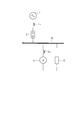
- FIG. 4 shows an example in which the existing power system (system higher than the power distribution system) 1 and the power distribution system (microgrid) 10 are connected via the line impedance Ls and the circuit breaker 2.
- a distributed power source 11 and a load 12 are connected to a power distribution system 10 that is a microgrid.
- the distributed power source 11 is illustrated as one generator in FIG. 4, it is actually driven by a natural energy type power generation facility (solar power generation facility, wind power generation facility, etc.) using natural energy and an internal combustion engine. It is comprised of a plurality of dispersed power generation facilities, including an internal combustion engine type power generation facility (such as a diesel power generation facility).
- the load 12 is actually a plurality of distributed loads.
- the microgrid 10 as shown in FIG. 4 has a natural energy type power generation facility, the amount of power generation varies greatly depending on the weather, wind speed, and the like. Therefore, a system stabilizing device is used for the purpose of absorbing the fluctuation of the power generation amount.
- the output power is adjusted by governor control.
- the response of the governor control is slow, when the electric power consumed by the load 12 fluctuates suddenly, the internal combustion engine type power generation equipment follows such a sudden fluctuation (rapid excess or deficiency) of the electric power. I can't.
- the system stabilizing device is also used for the purpose of assisting the internal combustion engine type power generation equipment and balancing the demand and supply of electric power by following such a rapid fluctuation of electric power with good responsiveness. Yes.
- the system stabilization device is a power conversion device having a power storage function, and is a device that is installed in the distribution system and performs the power compensation described above.
- FIG. 5 is an example in which one system stabilizing device 20 is provided in the power distribution system (microgrid) 10 shown in FIG.
- the system stabilizing device 20 is connected to the distributed power supply 11 and the load 12 in parallel.
- the system stabilizing device 20 includes a control unit 21, a power converter 22 that can perform a reverse conversion operation and a forward conversion operation, and a DC charging unit 23 such as an electric double layer capacitor or a lead storage battery.
- the power converter 22 operates according to the gate signal g sent from the control unit 21.
- the power converter 22 converts the AC power obtained from the power distribution system 10 into DC power and converts the DC power to DC.
- the charging unit 23 and performing a reverse conversion operation the DC power charged in the DC charging unit 23 is converted into AC power, and the AC power is sent to the distribution system 10.
- the system current Is flowing into the distribution system 10 from the power system 1 is detected by the current detector 24, and the system voltage Vs that is the voltage of the distribution system 10 is detected by the voltage detector 25.
- a converter current Iinv input / output by the power converter 22 is detected by a current detector 26.
- this system stabilizing device 20 when the power system 1 is in a normal state where a failure or the like has not occurred, the circuit breaker 2 is connected and the operation is performed with the power distribution system 10 connected to the power system 1. System operation "is performed. During this grid interconnection operation, power is supplied to the load 12 by the power system 1, the distributed power supply 11, and the system stabilization device 20.
- the grid stabilization device 20 operates as follows during grid-connected operation and autonomous operation. (1) At the time of grid connection operation, the grid stabilization device 20 detects the grid current Is flowing into the distribution system 10, obtains grid power from the grid current Is, and suppresses fluctuations in the grid power. Operate. (2) During the independent operation, the system stabilizing device 20 detects the system voltage Vs in the distribution system 10 and performs a compensation operation so that the voltage amplitude and frequency of the system voltage Vs are stabilized.
- the phase synchronization circuit (PLL) 101 outputs a reference phase signal ⁇ indicating the phase of the system voltage Vs from the system voltage Vs.
- the sine wave generator 102 outputs a reference sine wave signal K having a rated voltage synchronized with the reference phase signal ⁇ .
- the change-over switch 103 has the movable contacts 103a and 103b on the A side as shown by the solid line in the figure, and in the independent operation, the movable contacts 103a and 103b are set to B as shown by the dotted line in the figure. To the side.
- the dq conversion unit 104 dq-converts the system current Is into a rotating coordinate system that rotates at the phase indicated by the reference phase signal ⁇ , and outputs an effective part Isd of the system current and an ineffective part Isq of the system current.
- the first variation detection block 105 detects the variation of the effective amount Isd of the system current on the dq axis and outputs this as the effective current command Irefd, and the second variation detection block 106 is on the dq axis.
- the fluctuation amount of the ineffective portion Isq of the system current is detected, and this is output as the ineffective portion current command Irefq.
- the fluctuation detection blocks 105 and 106 are band-pass filters having a differentiation function and a filter function, and details of the structure will be described later.
- the dq converter 107 dq-converts the converter current Iinv into a rotating coordinate system that rotates at the phase indicated by the reference phase signal ⁇ , and outputs the effective part Iinvd of the converter current and the ineffective part Iinvq of the converter current.
- the subtracting unit 108 subtracts the effective amount Iinvd of the converter current from the effective current command Irefd and outputs the effective current deviation ⁇ d.
- the subtractor 109 subtracts the ineffective portion Iinvq of the converter current from the ineffective current command Irefq and outputs the ineffective current deviation ⁇ q.
- the current control unit 110 performs proportional integral (PI) control on the effective current deviation ⁇ d and outputs an effective voltage command Vd.
- the current control unit 111 performs proportional integral (PI) control on the current deviation ⁇ q corresponding to the ineffective part and outputs a voltage command Vq corresponding to the ineffective part.
- the dq reverse conversion unit 112 performs dq reverse conversion on the valid voltage command Vd and the invalid voltage command Vq, and outputs a voltage command in a fixed coordinate system.
- the adder 113 adds the reference sine wave signal K to the fixed coordinate system voltage command output from the dq inverse transform unit 112, and outputs a fixed coordinate system voltage command V * .
- a PWM (Pulse Width Modulation) modulator 114 PWM modulates the voltage command V * and outputs a gate signal g. Operation control of the power converter 22 is performed by the gate signal g, and power is output from the power converter 22 in order to suppress fluctuations in the grid current Is during grid interconnection operation.
- the frequency detector 121 detects the frequency of the system voltage Vs and outputs a frequency signal F. Note that the frequency of the system voltage Vs corresponds to the active power, and when the active power decreases, the frequency of the system voltage Vs decreases, and when the active power increases, the frequency of the system voltage Vs increases.
- the amplitude detector 122 detects the amplitude of the system voltage Vs and outputs an amplitude signal L. Note that the amplitude of the system voltage Vs corresponds to the reactive power, and when the reactive power decreases, the amplitude of the system voltage Vs decreases, and when the reactive power increases, the amplitude of the system voltage Vs increases.
- the third variation detection block 123 detects the variation of the frequency signal F and outputs this as an effective current command Irefd
- the fourth variation detection block 124 detects the variation of the amplitude signal L. This is output as an invalid current command Irefq.
- the fluctuation detection blocks 123 and 124 are band-pass filters having a differentiation function and a filter function, and details of the structure will be described later.
- the subtracting unit 108 subtracts the effective amount Iinvd of the converter current from the effective current command Irefd and outputs the effective current deviation ⁇ d.
- the subtractor 109 subtracts the ineffective portion Iinvq of the converter current from the ineffective current command Irefq and outputs the ineffective current deviation ⁇ q.
- the current control unit 110 performs proportional integral (PI) control on the effective current deviation ⁇ d and outputs an effective voltage command Vd.
- the current control unit 111 performs proportional integral (PI) control on the invalid current deviation ⁇ q, and outputs the invalid voltage command Vq.
- the dq reverse conversion unit 112 performs dq reverse conversion on the valid voltage command Vd and the invalid voltage command Vq, and outputs a voltage command in a fixed coordinate system.
- the adder 113 adds the reference sine wave signal K to the fixed coordinate system voltage command output from the dq inverse transform unit 112, and outputs a fixed coordinate system voltage command V * .
- a PWM (Pulse Width Modulation) modulator 114 PWM modulates the voltage command V * and outputs a gate signal g. Operation control of the power converter 22 is performed by the gate signal g, and power is output from the power converter 22 in order to suppress fluctuations in the voltage amplitude and frequency of the system voltage Vs during the independent operation.
- the fluctuation detection blocks 105, 106, 123, and 124 are configured by bandpass filters.
- the configuration of a conventional band-pass filter 50 that can be used as the fluctuation detection blocks 105, 106, 123, and 124 will be described with reference to FIG.
- s is a Laplace operator indicating a differentiation function.
- the band pass filter (variation detection block) 50 includes a low pass filter 51, a low pass filter 52, and a subtractor 53.
- the passband frequency of the bandpass filter 50 is determined in accordance with the filtering characteristics required for each fluctuation detection block 105, 106, 123, 124. Further, the cutoff frequency on the high frequency side of the determined passband frequency is f1, and the cutoff frequency on the low frequency side is f2.
- the low-pass filter 51 for noise removal has a cutoff frequency of f1 and a time constant of T1.
- the low-pass filter 51 is a filter having a first-order lag characteristic, and its time constant is a time constant T1 determined for the purpose of noise removal.
- the low-pass filter 52 is a filter having a first-order lag characteristic, and its time constant is a time constant T2 determined for the purpose of setting a time for detecting fluctuations.
- both filters 51 and 52 filter the input signal using the respective filter characteristics.
- the bandpass filter (variation detection block) 50 is the variation detection block 105
- the input signal is the effective portion Isd of the system current.
- the bandpass filter (variation detection block) 50 is the variation detection block 106
- the input signal is the ineffective portion Isq of the system current.
- the bandpass filter (variation detection block) 50 is the variation detection block 123, the input signal is the frequency signal F.
- the bandpass filter (variation detection block) 50 is the variation detection block 124, the input signal is the amplitude signal L.
- the subtractor 53 outputs a signal obtained by subtracting the signal output from the low-pass filter 52 from the signal output from the low-pass filter 51.
- the signal output from the subtracter 53 is a fluctuation signal.
- the bandpass filter (variation detection block) 50 is the variation detection block 105
- the variation signal is an effective current command I refd that is a variation of the effective amount Isd of the system current.
- the band-pass filter (variation detection block) 50 is the variation detection block 106
- the variation signal is an invalid current command I refq that is a variation of the invalid portion Isq of the system current.
- the band pass filter (variation detection block) 50 is the variation detection block 123
- the variation signal is an effective current command I refd that is the variation of the frequency signal F.
- the band-pass filter (variation detection block) 50 is the variation detection block 124
- the variation signal is an invalid current command I refq that is a variation of the amplitude signal L.
- FIG. 8 shows an example in which the power distribution system (microgrid) 10 shown in FIG. 4 includes two system stabilizing devices 20-1 and 20-2.
- the system stabilizing devices 20-1 and 20-2 are connected in parallel to the distributed power supply 11 and the load 12.
- the system stabilizing devices 20-1 and 20-2 have the same configuration as the system stabilizing device 20 shown in FIG.
- the DC charging unit 23-1 provided in the system stabilizing device 20-1 is an electric double layer capacitor
- the DC charging unit 23-2 provided in the system stabilizing device 20-2 is a lead storage battery.
- the control unit 21-1 of the system stabilizing device 20-1 has the same configuration as the control unit 21 shown in FIG. 6, and the system current Is detected by the current detector 24 and the voltage detector 25-1 The detected system voltage Vs1 and the converter current Iinv1 detected by the current detector 26-1 are taken in and the gate signal g1 is output.
- the power converter 22-1 performs a forward conversion operation according to the gate signal g1
- the AC power obtained from the distribution system 10 is converted into DC power, and this DC power is converted into a DC charging unit (electric double layer capacitor).
- the DC power charged in the DC charging unit (electric double layer capacitor) 23-1 is converted into AC power, and this AC power is sent to the distribution system 10.
- the control unit 21-1 includes variation detection blocks 105, 106, 123, and 124, similarly to the control unit 21 shown in FIG.
- the DC charging unit 23-1 of the system stabilizing device 20-1 is an electric double layer capacitor having a small storage capacity, although it does not affect the life even when high-speed charging / discharging is performed. For this reason, the system stabilizing device 20-1 using an electric double layer capacitor as the DC charging unit 23-1 compensates for power fluctuations by performing charging and discharging at high speed in a short time.
- the control unit 21-2 of the system stabilizing device 20-2 has the same configuration as the control unit 21 shown in FIG. 6, and the system current Is detected by the current detector 24 and the voltage detector 25-2.
- the detected system voltage Vs2 and the converter current Iinv2 detected by the current detector 26-2 are taken in and the gate signal g2 is output.
- the power converter 22-2 performs a forward conversion operation according to the gate signal g2
- the AC power obtained from the power distribution system 10 is converted into DC power
- the DC power is converted into a DC charging unit (lead storage battery) 23-.
- the battery 2 is charged and the reverse conversion operation is performed, the DC power charged in the DC charging unit (lead storage battery) 23-2 is converted into AC power, and the AC power is sent to the distribution system 10.
- the control unit 21-2 includes fluctuation detection blocks 105, 106, 123, and 124, similarly to the control unit 21 shown in FIG.
- the DC charging unit 23-2 of the system stabilizing device 20-2 is a lead storage battery that can be charged and discharged for a long time, but deteriorates its life when deep charging and discharging are performed in a short time. For this reason, the system stabilizing device 20-2 using an electric double layer capacitor as the DC charging unit 23-2 does not perform charging / discharging at high speed in a short time, and starts up charging / discharging over time. Charge and discharge for hours.
- the outputs of the system stabilization apparatus 20-1, the system stabilization apparatus 20-2, and the distributed power supply 11 are output.
- the power and output current are monitored, and the system stabilizing device 20-1, the system stabilizing device 20-2, and the distributed power source 11 are commanded to output power and output current, respectively. It is necessary to control the operation of the generator 20-1, the system stabilizer 20-2, and the distributed power supply 11.
- Patent Document 2 Japanese Patent Application Laid-Open No. 2006-333563 discloses a technique for cooperatively operating a plurality of types of distributed power supplies. By using the technique shown in Patent Document 2, two system stabilizing devices 20 are disclosed. -1,20-2 can be operated.
- monitoring means for monitoring the output power and output current of the system stabilizing device 20-1, the system stabilizing device 20-2, and the distributed power source 11, and each system stabilizing device and the distributed power source according to the monitoring result There is a problem that a control means for controlling the operation is further required.
- the present invention provides a system stabilizing device without monitoring each system stabilizing device or distributed power source even if the power distribution system includes a plurality of system stabilizing devices having different charge / discharge characteristics. It is an object of the present invention to provide a system stabilization device capable of preventing system interference and performing stable system stabilization control.
- the configuration of the present invention for solving the above problems is as follows. It is a system stabilizing device that is connected to the power system when the power system is normal, is disconnected from the power system when an abnormality occurs in the power system, and is provided in a power distribution system to which a distributed power source and a load are connected. And
- the system stabilizing device includes a control unit and a power converter that performs a forward conversion operation and an inverse conversion operation according to a gate signal transmitted from the control unit,
- the controller is When the power system is normal, From the system current flowing into the distribution system from the power system, find the effective part of the system current and the ineffective part of the system current, The first variation detection block obtains the variation included in the effective portion of the system current, and this variation is used as the effective current command.
- the second fluctuation detection block obtains the fluctuation included in the invalid portion of the grid current, and this fluctuation is used as the invalid current command. Further, from the converter current input and output by the power converter, an effective part of the converter current and an ineffective part of the converter current are obtained, An effective current deviation that is a deviation between the effective current command and the effective current of the converter is set to zero, and an invalidity that is a deviation between the invalid current command and the invalid current of the converter current.
- an effective part of the converter current and an ineffective part of the converter current are obtained from the converter current input and output by the power converter,
- An effective current deviation that is a deviation between the effective current command and the effective current of the converter is set to zero, and an invalidity that is a deviation between the invalid current command and the invalid current of the converter current.
- the first to fourth fluctuation detection blocks are A fluctuation detection unit (300) that outputs a common current command, a first current command creation unit (400) that inputs the common current command and outputs a first current command, and the common current command And a second current command generating unit (500) for inputting and outputting a second current command.
- the fluctuation detection unit (300) includes a low-pass filter (301) in which a time constant determined for the purpose of noise removal is set and a signal change value per unit time when a change occurs in the value of the input signal.
- a cushion circuit (310) that outputs a signal and a subtracter (303) that subtracts the output signal of the cushion circuit (301) from the output signal of the low-pass filter (301) and outputs the common current command.
- the first current command generation unit (400) receives a signal change value per unit time when the common current command is input and a change occurs in the value of the input signal, as a signal of the cushion circuit (310).
- a cushion circuit (410) that outputs a signal with a larger value than the change value, a subtracter (401) that subtracts and outputs the output signal of the cushion circuit (410) from the common current command, and the subtractor ( 401) an amplifier (402) for amplifying the output signal, an amplifier (403) for amplifying the output signal of the cushion circuit (410), a rated limiter (404) for limiting the output signal of the amplifier (403),
- the output signal of the rated limiter (404) is input and a change occurs in the value of the input signal, the signal change value per unit time is made larger than the signal change value of the cushion circuit (310) to generate a signal.
- Output cushion circuit (420) and the rated limiter (404) A subtractor (405) that subtracts and outputs the output signal of the cushion circuit (420) from the output signal, and adds the output signal of the amplifier (402) and the output signal of the subtractor (405) to the first signal.
- An adder (406) that outputs a current command of The second current command generation unit (500) includes an amplifier (501) that amplifies the common current command, a rating limiter (502) that limits an output signal of the amplifier (501), and the rating limiter (502). ) And the second current command is set by making the signal change value per unit time larger than the signal change value of the cushion circuit (310) when a change occurs in the value of the input signal. It has a cushion circuit (510) for outputting.
- the configuration of the present invention is as follows.
- a changeover switch (408) is interposed between the subtracter (405) and the adder (406),
- This changeover switch (408) A system stabilizing device in which the DC charging unit connected to the power converter is formed of an electric double layer capacitor, and a system stabilizing device in which the DC charging unit connected to the power converter is formed of a lead storage battery Is in the on state when and When only the system stabilizing device in which the DC charging unit connected to the power converter is formed of an electric double layer capacitor is operating alone, the system is cut off.
- the configuration of the present invention is as follows.
- the cushion circuits (310), (410), (420) and (510) are ⁇ (X ⁇ Ts / Tc) when the cushion time is Tc, the sample period is Ts, and X is a limit value.
- the subtractor delays the input signal of the cushion circuit from the input signal. Subtract the circuit output signal and send it to the limiter,
- the adder adds and outputs the output signal of the limiter and the output signal of the delay circuit,
- the delay circuit delays the signal output from the adder by one sample period Ts and outputs the delayed signal.
- the cushion time (T3) set for the limiter of the cushion circuit (310) is set longer than the cushion time (T4) set for the limiter of the cushion circuit (410), (420), (510). It is characterized by being.
- the configuration of the present invention is as follows.
- a system stabilizing device as described above,
- the time constant for noise removal is set as T1
- the time constant for setting the fluctuation detection time is set as T2
- the arbitrarily set first cushion is T3.
- a second cushion time shorter than the first cushion time T3 is set as T4,
- the fluctuation detection unit (300) is calculated by an arithmetic process using an arithmetic processing program.
- a first-order lag filter process is performed on the input signal input to the fluctuation detection block with a time constant T1 to obtain a first filter signal
- the input signal input to the fluctuation detection block is subjected to first-order lag filtering with a time constant of T2, to obtain a second filter signal
- the signal change value per unit time is moderated using the first cushion time T3 to obtain the cushion signal (a)
- Subtracting the cushion signal (a) from the first filter signal to obtain a common current command (I rdfd0 )
- the first current command creation unit (400) performs arithmetic processing using an arithmetic processing program
- a common current command (I rdfd0 ) is used to obtain a cushion signal (b) by gradually reducing the signal change value per unit time using the second cushion time T4.
- the second current command generation unit (500) performs arithmetic processing using an arithmetic processing program, After limiting the common current command (I rdfd0 ) with a preset rated value, the signal change value per unit time is moderated using the second cushion time T4, and the current command (I fdfd2 ) is obtained. A current command (I fdfd2 ) is output.
- the first current control command having a short charge / discharge time and the second current control command having a long charge / discharge time are obtained from the fluctuation detection block incorporated in the control unit of the system stabilizing device.
- the first current command in the system stabilization device with the electric double layer capacitor as a DC charging unit it is possible to perform high-speed charge and discharge in a short time suitable for the charge and discharge characteristics of the electric double layer capacitor.
- the system stabilization device using a lead-acid battery as a direct current charging unit uses the second current command to start charging / discharging over time and charge / discharge for a long time, suitable for the charge / discharge characteristics of the lead-acid battery. be able to.
- the cushion circuit with a limiter, delay circuit, subtractor, and adder, the current command change obtained is a linear characteristic (linear change).
- various devices generators that operate in conjunction with the system stabilizing device.
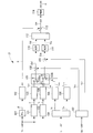
- FIG. 1 is a circuit diagram showing a fluctuation detection block according to Embodiment 1 of the present invention.
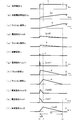
- the characteristic view which shows the current characteristic when Example 1 is used.
- the circuit diagram which shows the fluctuation
- the circuit block diagram which shows a microgrid.
- the circuit block diagram which shows the microgrid provided with one system stabilization apparatus.
- the circuit diagram which shows the control part of a system
- FIG. 1 shows a fluctuation detection block 200 according to the first embodiment of the present invention.
- the fluctuation detection block 200 includes first to fourth fluctuation detection blocks 105, 106, 106 incorporated in the control units 21-1, 21-2 (see FIG. 8) of the system stabilizing devices 20-1, 20-2. 123 and 124 (see FIG. 6).
- the fluctuation detecting block 200 includes a fluctuation detecting unit 300, a first current command creating unit 400, and a second current command creating unit 500.
- the fluctuation detection block 200 can be used as the fluctuation detection blocks 105, 106, 1230, and 124 shown in FIG. (1)
- the fluctuation detection unit 300 receives the effective portion Isd of the system current and generates the first and second current commands. Units 400 and 500 output an effective current command Irefd.
- the fluctuation detection unit 300 receives the invalid portion Isq of the system current and generates the first and second current commands. Units 400 and 500 output an invalid current command Irefq.
- the fluctuation detection block 200 is used as the fluctuation detection block 123 (see FIG.
- the frequency signal F is input to the fluctuation detector 300, and the first and second current command generators 400, From 500, an effective current command Irefd is output.
- the fluctuation detection block 200 is used as the fluctuation detection block 124 (see FIG. 6)
- the amplitude signal L is input to the fluctuation detection unit 300, and the first and second current command generation units 400, From 500, an invalid current command Irefq is output.
- the current command Irefd or the current command Irefq is output from the first and second current command generators 400 and 500 of the fluctuation detection block 200, respectively.
- the current command is used as follows. (1) When the fluctuation detection block 200 is used as a fluctuation detection block of the system stabilizing device 20-1 using an electric double layer capacitor as a DC charging unit, the current output from the first current command generation unit 400 The command Irefd1 or the current command Irefq1 is used, and the current command Irefd2 or the current command Irefq2 output from the second current command generation unit 500 is not used.
- the current command Irefd2 output from the second current command generation unit 500
- the current command Irefq2 is used, and the current command Irefd1 or the current command Irefq1 output from the first current command creation unit 400 is not used.
- the fluctuation detection block 200 is used as the fluctuation detection block 105 (see FIG. 6)
- the fluctuation detection block 200 may be used as the fluctuation detection blocks 106, 123, and 124 (see FIG. 6). Can be used.
- the fluctuation detection block 200 When this fluctuation detection block 200 is used as the fluctuation detection block 105 (see FIG. 6), the fluctuation detection block 200 receives an effective portion Isd of the system current, and the fluctuation detection block 200 receives the current command Irefd1 and the current. Command Irefd2 is output.
- the input / output state of each part 300, 400, 500 of the fluctuation detection block 200 will be described as follows.
- the fluctuation detection unit 300 inputs an effective part Isd of the system current and outputs a common current command Irefd0.
- the first current command generator 400 receives the common current command Irefd0 and outputs the current command Irefd1.
- the current command Irefd1 has a characteristic that rises instantaneously when there is a load change and linearly decreases (gradually decreases) over time T4.
- This current command Irefd1 is used as a current command for the system stabilizing device 20-1 provided with the DC charging unit 23-1 composed of an electric double layer capacitor.
- the second current command creation unit 500 inputs a common current command Irefd0 and outputs a current command Irefd2.
- the current command Irefd2 has a characteristic of increasing (gradual increase) linearly over time T4 and then decreasing linearly (gradual decrease) over time (T3-T4) when there is a load change. Yes.
- This current command Irefd2 is used as a current command for the system stabilizing device 20-2 including the DC charging unit 23-2 formed of a lead storage battery.
- the fluctuation detection unit 300 includes a low-pass filter 301, a low-pass filter 302, a subtractor 303, and a cushion circuit 310.
- the cushion circuit 310 includes a limiter 311, a delay circuit 312, a subtracter 313, and an adder 314.
- the low-pass filter 301 is a filter having a first-order lag characteristic whose time constant is the time constant T1.
- the time constant T1 is a time constant determined for the purpose of noise removal.
- the low-pass filter 301 filters the input signal using the filter characteristics.
- the low-pass filter 302 is a filter having a first-order lag characteristic whose time constant is the time constant T2.
- the time constant T2 is a time constant determined for the purpose of setting the fluctuation detection time.
- the low-pass filter 302 filters the input signal using the filter characteristics.
- the limiter 311 of the cushion circuit 310 has a limit characteristic of ⁇ (X ⁇ Ts / T3).
- T3 is a cushion time set to an arbitrary time
- Ts is one sample period
- X is a limit value.
- the charge / discharge time of the system stabilizing device 20-2 including the DC charging unit 23-2 using a lead storage battery is set by the cushion time T3.
- the limiter 311 limits the amount of change per sample period Ts.
- the limiter 311 holds the signal value of the input signal as it is.
- the signal value of the output signal and input to the limiter 311 is greater than or equal to + X (upper limit value)
- the value increases with a constant slope for a predetermined time, and then the value is limited to + X.
- the signal value of the signal input to the limiter 311 is equal to or less than ⁇ X (lower limit value)
- the value decreases with a constant slope for a predetermined time, and thereafter the value is limited to ⁇ X. .
- the delay circuit 312 has a characteristic of delaying the input signal by one sample period Ts and outputting it.
- the delay circuit 312 can be configured by, for example, a Z conversion circuit having a characteristic of Z ⁇ 1 .
- the subtractor 313 subtracts the output signal of the delay circuit 312 from the output signal of the low-pass filter 302 having the first-order lag characteristic, and sends the subtracted signal to the limiter 311. That is, the output signal of the delay circuit 312 is negatively fed back before the limiter 311.
- the adder 314 adds the signal output from the limiter 311 and the signal output from the delay circuit 312 and outputs the result. That is, the output signal of the delay circuit 312 is positively fed back at the subsequent stage of the limiter 311.
- the delay circuit 312 delays and outputs the output signal of the adder 314 by one sample period Ts.
- the signal state is as follows.
- the output of the subtracter 313 is “the current sample value minus the value after the limiter process before the sample period”. Therefore, when the signal value input from the low pass filter 302 to the subtractor 313 is + X or less and ⁇ X or more, the signal value output from the limiter 311 is zero. On the other hand, when the signal value input from the low pass filter 302 to the subtractor 313 is greater than or equal to + X or less than or equal to ⁇ X, the upper limit value / lower limit value of the signal value output from the limiter 311 is the limit value (+ X , -X).
- the output of the adder 314 is “the output of the limiter + 1 the value after the limiter process before the sampling period”. Therefore, when the signal value input from the low-pass filter 302 to the subtracter 313 is greater than or equal to + X or less than or equal to ⁇ X, the signal value output from the adder 314 increases linearly. That is, the signal value output from the adder 314 changes (increases or decreases) step by step by the limit value (+ X or ⁇ X) every sample period Ts.
- the cushion circuit 310 outputs a signal with a gradual signal change value per unit time when a change occurs in the value of the input signal.
- the subtractor 303 subtracts the output signal of the adder 314 from the output signal of the low-pass filter 301 having the first-order lag characteristic and outputs the result. From the subtractor 303, the variation included in the input signal is output. In this example, a common current command Irefd0 corresponding to the variation of the effective amount Isd of the system current is output from the subtractor 303 (variation detector 300).
- the signal state shown in FIG. 2 is a state when the load suddenly increases and the load current IL increases stepwise as shown in FIG.
- the effective portion Isd of the system current rises instantaneously at the load fluctuation time t1, and thereafter increases linearly (gradual increase) until time t3 over time T3.
- the system stabilization control (current compensation) operation is performed by the system stabilization devices 20-1 and 20-2.
- the effective amount Ids of the system current is filtered by the low-pass filter 302 and further cushioned by the cushion circuit 310 so that the signal change value per unit time is moderated.
- a cushion signal a as shown in c) is output.
- the subtractor 303 outputs a common current command Irefd0 as shown in FIG. 2D by subtracting the cushion signal a from the effective amount Isd of the system current.
- the first current command generation unit 400 includes a subtractor 401, amplifiers 402 and 403, a rating limiter 404, a subtracter 405, an adder 406, a rating limiter 407, and cushion circuits 410 and 420. ing.
- the cushion circuits 410 and 420 include limiters 411 and 421, delay circuits 412 and 422, subtracters 413 and 423, and adders 414 and 424, respectively.
- the limiters 411 and 421 of the cushion circuits 410 and 420 have limit characteristics of ⁇ (X ⁇ Ts / T4), respectively.
- T4 is a cushion time set to an arbitrary time shorter than time T3, Ts is one sample period, and X is a limit value. Note that the charge / discharge time of the system stabilizing device 20-1 including the DC charging unit 23-1 by the electric double layer capacitor is set by the cushion time T4.
- the operation of the cushion circuits 410 and 420 is basically the same as that of the cushion circuit 310, although the cushion time is different. That is, when a change occurs in the value of the input signal, the signal change value per unit time is made larger than the signal change value of the cushion circuit 310 and a signal is output.
- the common current command Irefd0 output from the fluctuation detection unit 300 is cushioned by the cushion circuit 410 so that the signal change value per unit time is moderated.
- the subtractor 401 outputs a common subtraction signal c as shown in FIG. 2 (f) by subtracting the cushion signal b from the common current command Irefd0.
- the amplifier 402 amplifies the subtraction signal c and outputs a current command Irefd11 as shown in FIG.
- the cushion signal b is amplified by the amplifier 403, and the signal value is limited to the rated value by the rated limiter 404, whereby a limiter signal d as shown in FIG.
- the cushion circuit 420 Since the limiter signal d is cushioned by the cushion circuit 420 and the signal change value per unit time is moderated, the cushion circuit 420 outputs a cushion signal e as shown in FIG.
- the cushion signal e has a characteristic that linearly increases (increases gradually) from time t1 to time t2 over time T4 and decreases (gradually decreases) straightly from time t2 to time t3 over time (T3-T4). ing.
- the subtractor 405 outputs a current command Irefd12 as shown in FIG. 2 (j) by subtracting the cushion signal e from the limiter signal d.
- the time during which this current command Irefd12 is output is T4.
- This current command Irefd12 is a current command for suppressing the remaining of the system current fluctuation when the system stabilization device 20-1 and the system stabilization device 20-2 are operating in a coordinated manner.
- the adder 406 adds the current command Irefd11 and the current command Irefd12 to output a current command Irefd1 as shown in FIG.
- the current command Irefd1 is output after the signal value is limited to the rated value by the rated limiter 407.
- the current command Irefd1 has a small signal width (the length of the time axis) as T4 and has a characteristic of rising in a short time and falling in a short time. Suitable for use as 20-1 current command.
- the current command Irefd11 has a characteristic that the signal width (length of the time axis) is extremely small (further smaller than T4), and rises in a very short time and falls in a short time. Yes. Therefore, the current command Irefd11 is output in response to the fluctuation sensitively, or the output is stopped. For this reason, when the system stabilization device 20-1 and the system stabilization device 20-2 are operating cooperatively, an appropriate current command Irefd11 is obtained by being influenced by the stabilization control on the system stabilization device 20-2 side. It may not be possible. Therefore, in order to prevent the current command Irefd11 from reacting excessively and becoming an appropriate current command, the current command Irefd12 is added to the current command Irefd11 to obtain the current command Irefd1.
- the second current command generation unit 500 includes an amplifier 501, rated limiters 502 and 503, and a cushion circuit 510.
- the limiter 511 of the cushion circuit 510 has a limit characteristic of ⁇ (X ⁇ Ts / T4).
- T4 is a cushion time set to an arbitrary time shorter than time T3
- Ts is one sample period
- X is a limit value.
- the operation of the cushion circuit 510 is basically the same as the cushion circuit 310, although the cushion time is different. That is, when a change occurs in the value of the input signal, the signal change value per unit time is made larger than the signal change value of the cushion circuit 310 and a signal is output.
- the common current command Irefd0 is amplified by the amplifier 501, the signal value is limited to the rated value by the rating limiter 502, and further the cushion process is performed by the cushion circuit 510 so that the signal change value per unit time is moderated. For this reason, the cushion circuit 510 outputs a current command Irefd2 as shown in FIG. The current command Irefd2 is output after the signal value is limited to the rated value by the rated limiter 503.
- the current command Irefd2 has a signal width (length of the time axis) as long as T3 and has a characteristic of rising at time T4 and then falling at time (T3-T4). It is suitable for use as a current command for the system stabilization device 20-2 that performs charging and discharging for a long time.
- the current command flow Irefd1 is output only during the period T4 (t1 to t2), and the current command Irefd2 gradually increases during the period T4 (t1 to t2) and gradually increases during the period T4-T3 (t2 to t3).
- the current command Irefd1 rises instantaneously at time t1 and gradually decreases thereafter, while the current command Irefd2 gradually increases from time t1.
- the current command Irefd1 decreases and the current command Irefd2 increases on the contrary, so that the current command Irefd1 can be smoothly replaced with the current command Irefd2.
- the system stabilizing device 20-1 that performs charging and discharging for a short time is controlled by the current command Irefd1, and the DC charging unit 23- configured by the lead storage battery is used. 2 is controlled by the current command Irefd2, the system stabilization control by the system stabilization apparatus 20-1 and the system stabilization apparatus 20-2 interferes with each other. Good control can be performed without doing so. In addition, in this case, it is not necessary to monitor the output power and output current of the system stabilizing device 20-1, the system stabilizing device 20-2, and the distributed power source 11.
- the cushion circuits 310, 410, 420, and 430 are replaced with limiters 311, 411, 421, 431, delay circuits 312, 412, 422, 432, subtractors 313, 413, 423, 433, and adder 314. , 414, 424, 434, the obtained current commands Irefd1, Irefd2 change linearly. Therefore, not only control of the system stabilization devices 20-1 and 20-2 but also control of various devices (generators) operating in conjunction with the system stabilization device can be easily performed.
- FIG. 3 shows a fluctuation detection block 200A according to the second embodiment of the present invention.
- This variation detection block 200A is obtained by further providing a changeover switch 408 to the variation detection block 200 shown in FIG.
- the changeover switch 408 is interposed between the subtracter 405 and the adder 406.
- the changeover switch 408 includes a system stabilizing device 20-1 in which the DC charging unit 23-1 is formed by an electric double layer capacitor, and a system stabilizing device 20- in which the DC charging unit 23-2 is formed by a lead storage battery. 2 is turned on, and when only the system stabilizing device 20-1 in which the DC charging unit 23-1 is formed by the electric double layer capacitor is operated alone, the system is cut off.
- the system stabilizing device 20-1 may charge / discharge for a time longer than the time T4.
- Example 1 2 is an example at the time of using the fluctuation
- the fluctuation detection blocks 106, 123, and 124 can be used.
- Irefd1, Irefd2 may be replaced with invalid current commands Irefq0, Irefq11, Irefq12, Irefq1, Irefq2.
- the effective component Ics of the system current may be replaced with the frequency signal F in FIGS.
- the effective amount Ics of the system current is changed to the amplitude signal L, and the current commands Irefd0, Irefd11, Irefd12, Irefd1, Irefd2 may be replaced with invalid current commands Irefq0, Irefq11, Irefq12, Irefq1, and Irefq2.
- the first and second embodiments can be realized by calculating using a calculation processing program (software) preset in a computer.
- an arithmetic processing program (software) for performing arithmetic processing necessary as the fluctuation detection blocks 200 and 200A is incorporated in a computer that is hardware. It can be configured as (set).
- the following arithmetic processing is executed by the arithmetic processing program.
- the time constant for noise removal is set as T1
- the time constant for setting the fluctuation detection time is set as T2
- the arbitrarily set first cushion is set as T3.
- the second cushion time shorter than the first cushion time T3 is set as T4.
- the fluctuation detection unit (300) can perform arithmetic processing using an arithmetic processing program.
- a first-order lag filter process is performed on the input signal input to the fluctuation detection block with a time constant T1 to obtain a first filter signal
- the input signal input to the fluctuation detection block is subjected to first-order lag filtering with a time constant of T2, to obtain a second filter signal
- the signal change value per unit time is moderated using the first cushion time T3 to obtain the cushion signal (a)
- the cushion signal (a) is subtracted from the first filter signal to obtain a common current command (I rdfd0 ).
- the first current command generation unit (400) performs arithmetic processing using an arithmetic processing program,
- a common current command (I rdfd0 ) is used to obtain a cushion signal (b) by gradually reducing the signal change value per unit time using the second cushion time T4.
- the limiter signal (d) is obtained by gradually reducing the signal change value per unit time using the second cushion time T4, and obtaining the cushion signal (e).
- the second current command generation unit (500) performs arithmetic processing using an arithmetic processing program, After limiting the common current command (I rdfd0 ) with a preset rated value, the signal change value per unit time is moderated using the second cushion time T4 to obtain the current command (I fdfd2 ). Outputs the current command (I fdfd2 ).
Landscapes
- Engineering & Computer Science (AREA)
- Power Engineering (AREA)
- Physics & Mathematics (AREA)
- General Physics & Mathematics (AREA)
- Automation & Control Theory (AREA)
- Inverter Devices (AREA)
- Supply And Distribution Of Alternating Current (AREA)
Abstract
Description
図4に、既存の電力系統(配電系統よりも上位の系統)1と配電系統(マイクログリッド)10とが、線路インピーダンスLsと遮断器2を介して接続された例を示す。
そこで、この発電量の変動を吸収する目的で系統安定化装置が用いられる。
電力変換器22は、制御部21から送られてくるゲート信号gに応じて動作し、順変換動作をするときには、配電系統10から得た交流電力を直流電力に変換してこの直流電力を直流充電部23に充電し、逆変換動作をするときには、直流充電部23に充電していた直流電力を交流電力に変換し、この交流電力を配電系統10に送る。
(1)系統連系運転時には、系統安定化装置20は、配電系統10に流入する系統電流Isを検出し、この系統電流Isから系統電力を求めて、この系統電力の変動を抑制するように動作する。
(2)自立運転時には、系統安定化装置20は、配電系統10内の系統電圧Vsを検出し、この系統電圧Vsの電圧振幅と周波数が安定となるように補償動作を行なう。
位相同期回路(PLL)101は、系統電圧Vsから系統電圧Vsの位相を示す基準位相信号θを出力する。正弦波発生器102は、基準位相信号θに同期した定格電圧となっている基準正弦波信号Kを出力する。
変動検出ブロック105,106は、微分機能とフィルタ機能を有するバンドバスフィルタであり、その構造の詳細は後述する。
このゲート信号gにより電力変換器22の動作制御が行なわれ、系統連系運転時において、系統電流Isの変動を抑制するために、電力変換器22から電力が出力される。
変動検出ブロック123,124は、微分機能とフィルタ機能を有するバンドバスフィルタであり、その構造の詳細は後述する。
このゲート信号gにより電力変換器22の動作制御が行なわれ、自立運転時において、系統電圧Vsの電圧振幅と周波数の変動を抑制するために、電力変換器22から電力が出力される。
ここで、変動検出ブロック105,106,123,124として用いることができる、従来のバンドパスフィルタ50の構成を図7を参照して説明する。なお図7においてsは微分機能を示すラプラス演算子である。
なお、バンドパスフィルタ50の通過帯域周波数は、各変動検出ブロック105,106,123,124に要求されるフィルタリング特性に応じて決定される。また、決定された通過帯域周波数の高周波数側の遮断周波数をf1、低周波数側の遮断周波数をf2とする。
このため、ノイズ除去用ローパスフィルタ51は、その遮断周波数をf1としており、その時定数をT1としている。また、変動検出時間を設定するためのローパスフィルタ52は、その遮断周波数をf2としており、その時定数をT2としている。なおf1=1/T1となっており、f2=1/T2となっている。
ローパスフィルタ52は、一次遅れ特性を有するフィルタであり、その時定数は、変動検出する時間を設定する目的として決定した時定数T2となっている。
両フィルタ51,52は、入力信号が入力されると、それぞれのフィルタ特性を利用して、入力信号をフィルタリングする。
なお、バンドパスフィルタ(変動検出ブロック)50が変動検出ブロック105であれば、入力信号は、系統電流の有効分Isdである。
バンドパスフィルタ(変動検出ブロック)50が変動検出ブロック106であれば、入力信号は、系統電流の無効分Isqである。
バンドパスフィルタ(変動検出ブロック)50が変動検出ブロック123であれば、入力信号は、周波数信号Fである。
バンドパスフィルタ(変動検出ブロック)50が変動検出ブロック124であれば、入力信号は、振幅信号Lである。
バンドパスフィルタ(変動検出ブロック)50が変動検出ブロック105であれば、変動分信号は、系統電流の有効分Isdの変動分である有効分の電流指令Irefdである。
バンドパスフィルタ(変動検出ブロック)50が変動検出ブロック106であれば、変動分信号は、系統電流の無効分Isqの変動分である無効分の電流指令Irefqである。
バンドパスフィルタ(変動検出ブロック)50が変動検出ブロック123であれば、変動分信号は、周波数信号Fの変動分である有効分の電流指令Irefdである。
バンドパスフィルタ(変動検出ブロック)50が変動検出ブロック124であれば、変動分信号は、振幅信号Lの変動分である無効分の電流指令Irefqである。
なお、制御部21-1は、図6に示す制御部21と同様に、変動検出ブロック105,106,123,124を有している。
なお、制御部21-2は、図6に示す制御部21と同様に、変動検出ブロック105,106,123,124を有している。
電力系統が正常であるときには前記電力系統に接続され、前記電力系統に異常が発生したときには前記電力系統から遮断され、しかも分散電源と負荷が接続された配電系統に備えられる系統安定化装置であって、
前記系統安定化装置は、制御部と、前記制御部から送られてくるゲート信号に応じて順変換動作と逆変換動作をする電力変換器を有し、
前記制御部は、
前記電力系統が正常であるときには、
前記電力系統から前記配電系統に流入する系統電流から、系統電流の有効分と系統電流の無効分を求め、
第1の変動検出ブロックにより前記系統電流の有効分に含まれる変動分を求めて、この変動分を有効分の電流指令とし、
第2の変動検出ブロックにより前記系統電流の無効分に含まれる変動分を求めて、この変動分を無効分の電流指令とし、
更に、前記電力変換器が入出力する変換器電流から、変換器電流の有効分と変換器電流の無効分を求め、
前記有効分の電流指令と前記変換器電流の有効分との偏差である有効分の電流偏差を零とし、且つ、前記無効分の電流指令と前記変換器電流の無効分との偏差である無効分の電流偏差を零とするゲート信号を出力し、
前記電力系統に異常が発生したときには、
前記配電系統の系統電圧から、系統電圧の周波数を示す周波数信号と系統電圧の振幅を示す振幅信号を求め、
第3の変動検出ブロックにより前記周波数信号に含まれる変動分を求めて、この変動分を有効分の電流指令とし、
第4の変動検出ブロックにより前記振幅信号に含まれる変動分を求めて、この変動分を無効分の電流指令とし、
更に、前記電力変換器が入出力する変換器電流から変換器電流の有効分と変換器電流の無効分を求め、
前記有効分の電流指令と前記変換器電流の有効分との偏差である有効分の電流偏差を零とし、且つ、前記無効分の電流指令と前記変換器電流の無効分との偏差である無効分の電流偏差を零とするゲート信号を出力し、
しかも、第1から第4の変動検出ブロックは、
共通の電流指令を出力する変動検出部(300)と、前記共通の電流指令を入力して第1の電流指令を出力する第1の電流指令作成部(400)と、前記共通の電流指令を入力して第2の電流指令を出力する第2の電流指令作成部(500)とで構成され、
前記変動検出部(300)は、ノイズ除去を目的として決定した時定数が設定されているローパスフィルタ(301)と、入力信号の値に変化が生じたときに単位時間当たりの信号変化値を緩やかにして信号を出力するクッション回路(310)と、前記ローパスフィルタ(301)の出力信号から前記クッション回路(301)の出力信号を減算して前記共通の電流指令を出力する減算器(303)を有し、
前記第1の電流指令作成部(400)は、前記共通の電流指令が入力されると共に入力信号の値に変化が生じたときに単位時間当たりの信号変化値を前記クッション回路(310)の信号変化値よりも大きくして信号を出力するクッション回路(410)と、前記共通の電流指令から前記クッション回路(410)の出力信号を減算して出力する減算器(401)と、前記減算器(401)の出力信号を増幅するアンプ(402)と、前記クッション回路(410)の出力信号を増幅するアンプ(403)と、前記アンプ(403)の出力信号をリミットする定格リミッタ(404)と、前記定格リミッタ(404)の出力信号が入力されると共に入力信号の値に変化が生じたときに単位時間当たりの信号変化値を前記クッション回路(310)の信号変化値よりも大きくして信号を出力するクッション回路(420)と、前記定格リミッタ(404)の出力信号から前記クッション回路(420)の出力信号を減算して出力する減算器(405)と、前記アンプ(402)の出力信号と前記減算器(405)の出力信号を加算して前記第1の電流指令を出力する加算器(406)を有し、
前記第2の電流指令作成部(500)は、前記共通の電流指令を増幅するアンプ(501)と、前記アンプ(501)の出力信号をリミットする定格リミッタ(502)と、前記定格リミッタ(502)の出力信号が入力されると共に入力信号の値に変化が生じたときに単位時間当たりの信号変化値を前記クッション回路(310)の信号変化値よりも大きくして前記第2の電流指令を出力するクッション回路(510)を有する、ことを特徴とする。
前記第1の電流指令作成部(400)には、前記減算器(405)と前記加算器(406)の間に切替スイッチ(408)が介装されており、
この切替スイッチ(408)は、
前記電力変換器に接続された直流充電部が電気二重層キャパシタで形成されている系統安定化装置と、前記電力変換器に接続された直流充電部が鉛蓄電池で形成されている系統安定化装置とが協調運転しているときには投入状態となり、
前記電力変換器に接続された直流充電部が電気二重層キャパシタで形成されている系統安定化装置のみが単独運転しているときには遮断状態となることを特徴とする。
前記クッション回路(310),(410),(420),(510)は、クッション時間をTc、1サンプル周期をTs、Xをリミット値としたときに、±(X・Ts/Tc)となったリミット特性を有するリミッタと、入力された信号を1サンプル周期Tsだけ遅延させて出力する遅延回路と、減算器と、加算器を有し
前記減算器は、当該クッション回路の入力信号から前記遅延回路の出力信号を減算して前記リミッタに送り、
前記加算器は、前記リミッタの出力信号と前記遅延回路の出力信号とを加算して出力し、
前記遅延回路は、前記加算器から出力された信号を1サンプル周期Tsだけ遅延させて出力し、
しかも、前記クッション回路(310)のリミッタに設定したクッション時間(T3)は、前記クッション回路(410),(420),(510) のリミッタに設定したクッション時間(T4)よりも長く設定していることを特徴とする。
前記の系統安定化装置であって、
第1から第4の変動検出ブロックには、ノイズ除去用の時定数がT1として設定され、変動検出時間を設定するための時定数がT2として設定され、任意に設定した第1のクッションがT3として設定され、第1のクッション時間T3よりも短い第2のクッション時間がT4として設定され、
前記変動検出部(300)は、演算処理プログラムを用いた演算処理により、
当該変動検出ブロックに入力される入力信号を、時定数をT1とした一次遅れフィルタ処理して、第1のフィルタ信号を求め、
当該変動検出ブロックに入力される入力信号を、時定数をT2とした一次遅れフィルタ処理して、第2のフィルタ信号を求め、
第2のフィルタ信号を、第1のクッション時間T3を用いて単位時間当たりの信号変化値を緩やかにして、クッション信号(a)を求め、
第1のフィルタ信号からクッション信号(a)を減算して、共通の電流指令(Irdfd0)を求め、
前記第1の電流指令作成部(400)は、演算処理プログラムを用いた演算処理により、
共通の電流指令(Irdfd0)を、第2のクッション時間T4を用いて単位時間当たりの信号変化値を緩やかにして、クッション信号(b)を求め、
共通の電流指令(Irdfd0)からクッション信号(b)を減算して減算信号(c)を求め、この減算信号(c)を増幅して電流指令(Ifdfd11)を求め、
クッション信号(b)を予め設定した定格値でリミットしてリミッタ信号(d)を求め、
リミッタ信号(d)を、第2のクッション時間T4を用いて単位時間当たりの信号変化値を緩やかにして、クッション信号(e)を求め、
リミッタ信号(d)からクッション信号(e)を減算して電流指令(Ifdfd12)を求め、
電流指令(Ifdfd11)と電流指令(Ifdfd12)を加算して電流指令(Ifdfd1)を求め、または電流指令(Ifdfd11)をそのまま電流指令(Ifdfd1)として求め、求めた電流指令(Ifdfd1)を出力し、
前記第2の電流指令作成部(500)は、演算処理プログラムを用いた演算処理により、
共通の電流指令(Irdfd0)を予め設定した定格値でリミットした後、第2のクッション時間T4を用いて単位時間当たりの信号変化値を緩やかにして、電流指令(Ifdfd2)を求め、この電流指令(Ifdfd2)を出力する、ことを特徴とする。
(1)変動検出ブロック200を変動検出ブロック105(図6参照)として使用する場合には、変動検出部300には、系統電流の有効分Isdが入力され、第1,第2の電流指令作成部400,500からは有効分の電流指令Irefdが出力される。
(2)変動検出ブロック200を変動検出ブロック106(図6参照)として使用する場合には、変動検出部300には、系統電流の無効分Isqが入力され、第1,第2の電流指令作成部400,500からは無効分の電流指令Irefqが出力される。
(3)変動検出ブロック200を変動検出ブロック123(図6参照)として使用する場合には、変動検出部300には、周波数信号Fが入力され、第1,第2の電流指令作成部400,500からは有効分の電流指令Irefdが出力される。
(4)変動検出ブロック200を変動検出ブロック124(図6参照)として使用する場合には、変動検出部300には、振幅信号Lが入力され、第1,第2の電流指令作成部400,500からは無効分の電流指令Irefqが出力される。
(1)変動検出ブロック200を、電気二重層キャパシタを直流充電部とする系統安定化装置20-1の変動検出ブロックとして使用する場合には、第1の電流指令作成部400から出力される電流指令Irefd1または電流指令Irefq1を使用し、第2の電流指令作成部500から出力される電流指令Irefd2または電流指令Irefq2は使用しない。
(2)変動検出ブロック200を、鉛蓄電池を直流充電部とする系統安定化装置20-2の変動検出ブロックとして使用する場合には、第2の電流指令作成部500から出力される電流指令Irefd2または電流指令Irefq2を使用し、第1の電流指令作成部400から出力される電流指令Irefd1または電流指令Irefq1は使用しない。
この変動検出ブロック200の各部300,400,500の入出力状態を先に説明すると、次のとおりである。
変動検出部300は、ローパスフィルタ301と、ローパスフィルタ302と、減算器303と、クッション回路310とで構成されている。
クッション回路310は、リミッタ311と、遅延回路312と、減算器313と、加算器314とで構成されている。
ローパスフィルタ301は、入力信号(系統電流の有効分Isd)が入力されると、そのフィルタ特性を利用して、入力信号をフィルタリングする。
ローパスフィルタ302は、時定数が、時定数T2となっている、一次遅れ特性を有するフィルタである。時定数T2は、変動検出時間を設定することを目的として決定した時定数である。
ローパスフィルタ302は、入力信号(系統電流の有効分Isd)が入力されると、そのフィルタ特性を利用して、入力信号をフィルタリングする。
なお、T3は、任意の時間に設定したクッション時間であり、Tsは1サンプル周期であり、Xはリミット値である。
なお、クッション時間T3により、鉛蓄電池による直流充電部23-2を備えた系統安定化装置20-2の充放電時間が設定される。
つまり、遅延回路312の出力信号を、リミッタ311の前段で負帰還している。
つまり、遅延回路312の出力信号を、リミッタ311の後段で正帰還している。
したがって、ローパスフィルタ302から減算器313に入力される信号値が、+X以下で-X以上である場合には、リミッタ311から出力される信号値は0となる。
一方、ローパスフィルタ302から減算器313に入力される信号値が、+X以上または-X以下である場合には、リミッタ311から出力される信号値は、その上限値・下限値がリミット値(+X,-X)で制限された値となる。
したがって、ローパスフィルタ302から減算器313に入力される信号値が、+X以上または-X以下である場合には、加算器314から出力される信号値は、直線的に増加していく。即ち、加算器314から出力される信号値は、1サンプル周期Ts毎に、リミット値の値(+Xまたは-X)だけ段階的に変化(増加または減少)していく。
この例では、系統電流の有効分Isdの変動分に相当する、共通の電流指令Irefd0が、減算器303(変動検出部300)から出力される。
第1の電流指令作成部400は、減算器401と、アンプ402,403と、定格リミッタ404と、減算器405と、加算器406と、定格リミッタ407と、クッション回路410,420とで構成されている。
クッション回路410,420は、それぞれ、リミッタ411,421と、遅延回路412,422と、減算器413,423と、加算器414,424とで構成されている。
なお、T4は、時間T3よりも短い任意の時間に設定したクッション時間であり、Tsは1サンプル周期であり、Xはリミット値である。
なお、クッション時間T4により、電気二重層キャパシタによる直流充電部23-1を備えた系統安定化装置20-1の充放電時間が設定される。
アンプ402は、減算信号cを増幅して、図2(g)に示すような電流指令Irefd11を出力する。
クッション信号eは、時点t1から時点t2まで時間T4をかけて直線的に増加(漸増し)時点t2から時点t3まで時間(T3-T4)をかけて直正的に減少(漸減)する特性となっている。
この電流指令Irefd12は、系統安定化装置20-1と系統安定化装置20-2が協調運転しているときに、系統電流変動の残留を抑制する電流指令となっている。
このため、系統安定化装置20-1と系統安定化装置20-2が協調運転しているときには、系統安定化装置20-2側の安定化制御により影響を受けて適切な電流指令Irefd11が得られなくなる可能性がある。
そこで、電流指令Irefd11が過敏反応して適切な電流指令とならなくなることを防止するため、電流指令Irefd11に電流指令Irefd12を加算して、電流指令Irefd1としている。
第2の電流指令作成部500は、アンプ501と、定格リミッタ502,503と、クッション回路510とで構成されている。
なお、T4は、時間T3よりも短い任意の時間に設定したクッション時間であり、Tsは1サンプル周期であり、Xはリミット値である。
電流指令流Irefd1は期間T4(t1~t2)においてのみ出力され、電流指令Irefd2は、期間T4(t1~t2)においては徐々に増加し、期間T4-T3(t2~t3)において徐々に増加する。
期間T4に着目すると、電流指令Irefd1は時点t1にて瞬時に立ち上がってその後は徐々に減少するのに対して、電流指令Irefd2は時点t1から徐々に増加している。このように、期間T4では、電流指令Irefd1が減少し、電流指令Irefd2が逆に増加しているため、電流指令Irefd1から電流指令Irefd2の入れ替えをスムーズに行うことができる。
しかも、この場合には、系統安定化装置20-1と系統安定化装置20-2と分散電源11の出力電力及び出力電流を監視する必要はない。
このため、系統安定化装置20-1,20-2の制御のみならず、この系統安定化装置と連動して動作する各種機器(発電機)などの制御を容易に行うことができる。
このように、単独運転時にはIrefd1=Irefd11となるため、電流指令Irefd1には、系統電流変動の残留を抑制する電流指令Irefd12が含まれない。
しかし、本願のように、系統安定化装置20-1のみが単独運転されているときに切替スイッチ408を遮断して、電流指令Irefd1=Irefd11として、系統電流変動の残留を抑制する電流指令Irefd12を含まないようにすれば、短時間の充放電を行う系統安定化装置20-1が、時間T4よりも長い時間にわたって充放電動作を行うことを防止することができる。
上記設定が完了後、変動検出ブロック200,200Aは、演算処理プログラムを用いた演算処理により、次のような演算処理をする。
当該変動検出ブロックに入力される入力信号を、時定数をT1とした一次遅れフィルタ処理して、第1のフィルタ信号を求め、
当該変動検出ブロックに入力される入力信号を、時定数をT2とした一次遅れフィルタ処理して、第2のフィルタ信号を求め、
第2のフィルタ信号を、第1のクッション時間T3を用いて単位時間当たりの信号変化値を緩やかにして、クッション信号(a)を求め、
第1のフィルタ信号からクッション信号(a)を減算して、共通の電流指令(Irdfd0)を求める。
共通の電流指令(Irdfd0)を、第2のクッション時間T4を用いて単位時間当たりの信号変化値を緩やかにして、クッション信号(b)を求め、
共通の電流指令(Irdfd0)からクッション信号(b)を減算して減算信号(c)を求め、この減算信号(c)を増幅して電流指令(Ifdfd11)を求め、
クッション信号(b)を予め設定した定格値でリミットしてリミッタ信号(d)を求め、
リミッタ信号(d)を、第2のクッション時間T4を用いて単位時間当たりの信号変化値を緩やかにして、クッション信号(e)を求め、
リミッタ信号(d)からクッション信号(e)を減算して電流指令(Ifdfd12)を求め、
電流指令(Ifdfd11)と電流指令(Ifdfd12)を加算して電流指令(Ifdfd1)を求め、または電流指令(Ifdfd11)をそのまま電流指令(Ifdfd1)として求め、求めた電流指令(Ifdfd1)を出力する。
共通の電流指令(Irdfd0)を予め設定した定格値でリミットした後、第2のクッション時間T4を用いて単位時間当たりの信号変化値を緩やかにして、電流指令(Ifdfd2)を求め、この電流指令(Ifdfd2)を出力する。
2 遮断器
10 配電系統
11 分散電源
12 負荷
20,20-1,20-2 系統安定化装置
21,21-1,21-2 制御部
22,22-1,22-2 電力変換器
23,23-1,23-2 直流充電部
24,26,26-1,26-2 電流検出器
25,25-1,25-2 電圧検出器
105,106,123,124,200,200A 変動検出ブロック
300 変動検出部
400 第1の電流指令作成部
500 第2の電流指令作成部
Claims (4)
- 電力系統が正常であるときには前記電力系統に接続され、前記電力系統に異常が発生したときには前記電力系統から遮断され、しかも分散電源と負荷が接続された配電系統に備えられる系統安定化装置であって、
前記系統安定化装置は、制御部と、前記制御部から送られてくるゲート信号に応じて順変換動作と逆変換動作をする電力変換器を有し、
前記制御部は、
前記電力系統が正常であるときには、
前記電力系統から前記配電系統に流入する系統電流から、系統電流の有効分と系統電流の無効分を求め、
第1の変動検出ブロックにより前記系統電流の有効分に含まれる変動分を求めて、この変動分を有効分の電流指令とし、
第2の変動検出ブロックにより前記系統電流の無効分に含まれる変動分を求めて、この変動分を無効分の電流指令とし、
更に、前記電力変換器が入出力する変換器電流から、変換器電流の有効分と変換器電流の無効分を求め、
前記有効分の電流指令と前記変換器電流の有効分との偏差である有効分の電流偏差を零とし、且つ、前記無効分の電流指令と前記変換器電流の無効分との偏差である無効分の電流偏差を零とするゲート信号を出力し、
前記電力系統に異常が発生したときには、
前記配電系統の系統電圧から、系統電圧の周波数を示す周波数信号と系統電圧の振幅を示す振幅信号を求め、
第3の変動検出ブロックにより前記周波数信号に含まれる変動分を求めて、この変動分を有効分の電流指令とし、
第4の変動検出ブロックにより前記振幅信号に含まれる変動分を求めて、この変動分を無効分の電流指令とし、
更に、前記電力変換器が入出力する変換器電流から変換器電流の有効分と変換器電流の無効分を求め、
前記有効分の電流指令と前記変換器電流の有効分との偏差である有効分の電流偏差を零とし、且つ、前記無効分の電流指令と前記変換器電流の無効分との偏差である無効分の電流偏差を零とするゲート信号を出力し、
しかも、第1から第4の変動検出ブロックは、
共通の電流指令を出力する変動検出部(300)と、前記共通の電流指令を入力して第1の電流指令を出力する第1の電流指令作成部(400)と、前記共通の電流指令を入力して第2の電流指令を出力する第2の電流指令作成部(500)とで構成され、
前記変動検出部(300)は、ノイズ除去を目的として決定した時定数が設定されているローパスフィルタ(301)と、入力信号の値に変化が生じたときに単位時間当たりの信号変化値を緩やかにして信号を出力するクッション回路(310)と、前記ローパスフィルタ(301)の出力信号から前記クッション回路(301)の出力信号を減算して前記共通の電流指令を出力する減算器(303)を有し、
前記第1の電流指令作成部(400)は、前記共通の電流指令が入力されると共に入力信号の値に変化が生じたときに単位時間当たりの信号変化値を前記クッション回路(310)の信号変化値よりも大きくして信号を出力するクッション回路(410)と、前記共通の電流指令から前記クッション回路(410)の出力信号を減算して出力する減算器(401)と、前記減算器(401)の出力信号を増幅するアンプ(402)と、前記クッション回路(410)の出力信号を増幅するアンプ(403)と、前記アンプ(403)の出力信号をリミットする定格リミッタ(404)と、前記定格リミッタ(404)の出力信号が入力されると共に入力信号の値に変化が生じたときに単位時間当たりの信号変化値を前記クッション回路(310)の信号変化値よりも大きくして信号を出力するクッション回路(420)と、前記定格リミッタ(404)の出力信号から前記クッション回路(420)の出力信号を減算して出力する減算器(405)と、前記アンプ(402)の出力信号と前記減算器(405)の出力信号を加算して前記第1の電流指令を出力する加算器(406)を有し、
前記第2の電流指令作成部(500)は、前記共通の電流指令を増幅するアンプ(501)と、前記アンプ(501)の出力信号をリミットする定格リミッタ(502)と、前記定格リミッタ(502)の出力信号が入力されると共に入力信号の値に変化が生じたときに単位時間当たりの信号変化値を前記クッション回路(310)の信号変化値よりも大きくして前記第2の電流指令を出力するクッション回路(510)を有する、
ことを特徴とする系統安定化装置。 - 請求項1において、
前記第1の電流指令作成部(400)には、前記減算器(405)と前記加算器(406)の間に切替スイッチ(408)が介装されており、
この切替スイッチ(408)は、
前記電力変換器に接続された直流充電部が電気二重層キャパシタで形成されている系統安定化装置と、前記電力変換器に接続された直流充電部が鉛蓄電池で形成されている系統安定化装置とが協調運転しているときには投入状態となり、
前記電力変換器に接続された直流充電部が電気二重層キャパシタで形成されている系統安定化装置のみが単独運転しているときには遮断状態となることを特徴とする系統安定化装置。 - 請求項1または請求項2において、
前記クッション回路(310),(410),(420),(510)は、クッション時間をTc、1サンプル周期をTs、Xをリミット値としたときに、±(X・Ts/Tc)となったリミット特性を有するリミッタと、入力された信号を1サンプル周期Tsだけ遅延させて出力する遅延回路と、減算器と、加算器を有し
前記減算器は、当該クッション回路の入力信号から前記遅延回路の出力信号を減算して前記リミッタに送り、
前記加算器は、前記リミッタの出力信号と前記遅延回路の出力信号とを加算して出力し、
前記遅延回路は、前記加算器から出力された信号を1サンプル周期Tsだけ遅延させて出力し、
しかも、前記クッション回路(310)のリミッタに設定したクッション時間(T3)は、前記クッション回路(410),(420),(510) のリミッタに設定したクッション時間(T4)よりも長く設定していることを特徴とする系統安定化装置。 - 請求項1または請求項2に記載の系統安定化装置であって、
第1から第4の変動検出ブロックには、ノイズ除去用の時定数がT1として設定され、変動検出時間を設定するための時定数がT2として設定され、任意に設定した第1のクッションがT3として設定され、第1のクッション時間T3よりも短い第2のクッション時間がT4として設定され、
前記変動検出部(300)は、演算処理プログラムを用いた演算処理により、
当該変動検出ブロックに入力される入力信号を、時定数をT1とした一次遅れフィルタ処理して、第1のフィルタ信号を求め、
当該変動検出ブロックに入力される入力信号を、時定数をT2とした一次遅れフィルタ処理して、第2のフィルタ信号を求め、
第2のフィルタ信号を、第1のクッション時間T3を用いて単位時間当たりの信号変化値を緩やかにして、クッション信号(a)を求め、
第1のフィルタ信号からクッション信号(a)を減算して、共通の電流指令(Irdfd0)を求め、
前記第1の電流指令作成部(400)は、演算処理プログラムを用いた演算処理により、
共通の電流指令(Irdfd0)を、第2のクッション時間T4を用いて単位時間当たりの信号変化値を緩やかにして、クッション信号(b)を求め、
共通の電流指令(Irdfd0)からクッション信号(b)を減算して減算信号(c)を求め、この減算信号(c)を増幅して電流指令(Ifdfd11)を求め、
クッション信号(b)を予め設定した定格値でリミットしてリミッタ信号(d)を求め、
リミッタ信号(d)を、第2のクッション時間T4を用いて単位時間当たりの信号変化値を緩やかにして、クッション信号(e)を求め、
リミッタ信号(d)からクッション信号(e)を減算して電流指令(Ifdfd12)を求め、
電流指令(Ifdfd11)と電流指令(Ifdfd12)を加算して電流指令(Ifdfd1)を求め、または電流指令(Ifdfd11)をそのまま電流指令(Ifdfd1)として求め、求めた電流指令(Ifdfd1)を出力し、
前記第2の電流指令作成部(500)は、演算処理プログラムを用いた演算処理により、
共通の電流指令(Irdfd0)を予め設定した定格値でリミットした後、第2のクッション時間T4を用いて単位時間当たりの信号変化値を緩やかにして、電流指令(Ifdfd2)を求め、この電流指令(Ifdfd2)を出力する、
ことを特徴とする系統安定化装置。
Priority Applications (2)
| Application Number | Priority Date | Filing Date | Title |
|---|---|---|---|
| JP2010511089A JP5141764B2 (ja) | 2008-05-09 | 2009-05-08 | 系統安定化装置 |
| US12/990,602 US8452462B2 (en) | 2008-05-09 | 2009-05-08 | System stabilizing device |
Applications Claiming Priority (2)
| Application Number | Priority Date | Filing Date | Title |
|---|---|---|---|
| JP2008123041 | 2008-05-09 | ||
| JP2008-123041 | 2008-05-09 |
Publications (1)
| Publication Number | Publication Date |
|---|---|
| WO2009136641A1 true WO2009136641A1 (ja) | 2009-11-12 |
Family
ID=41264695
Family Applications (1)
| Application Number | Title | Priority Date | Filing Date |
|---|---|---|---|
| PCT/JP2009/058703 Ceased WO2009136641A1 (ja) | 2008-05-09 | 2009-05-08 | 系統安定化装置 |
Country Status (3)
| Country | Link |
|---|---|
| US (1) | US8452462B2 (ja) |
| JP (1) | JP5141764B2 (ja) |
| WO (1) | WO2009136641A1 (ja) |
Cited By (7)
| Publication number | Priority date | Publication date | Assignee | Title |
|---|---|---|---|---|
| JP2010119250A (ja) * | 2008-11-14 | 2010-05-27 | Meidensha Corp | 系統安定化装置 |
| US20120004787A1 (en) * | 2010-06-30 | 2012-01-05 | Hitachi, Ltd. | Method and apparatus for control battery and specification determining method of battery |
| WO2017037925A1 (ja) * | 2015-09-03 | 2017-03-09 | 株式会社東芝 | 電圧変動抑制装置及び方法 |
| JP2017508428A (ja) * | 2014-01-08 | 2017-03-23 | アーベーベー・リサーチ・リミテッドAbb Research Ltd. | ハイブリッドエネルギ蓄積システムを制御する方法および装置 |
| CN107465204A (zh) * | 2017-08-31 | 2017-12-12 | 中国电力科学研究院 | 一种储能电站中多电池组功率优化分配方法和装置 |
| WO2023218530A1 (ja) | 2022-05-10 | 2023-11-16 | 三菱電機株式会社 | 電力制御システム |
| WO2023238332A1 (ja) | 2022-06-09 | 2023-12-14 | 三菱電機株式会社 | エネルギー蓄積システム、および電力制御システム |
Families Citing this family (2)
| Publication number | Priority date | Publication date | Assignee | Title |
|---|---|---|---|---|
| DE102019133566A1 (de) | 2019-12-09 | 2021-06-10 | Rwe Renewables Gmbh | Verfahren sowie Stabilisierungsregler zum Betreiben eines Inselnetzes |
| CN114172209B (zh) * | 2021-11-29 | 2023-08-01 | 国网福建省电力有限公司电力科学研究院 | 基于滑动窗滤波和容量自适应分配的冲击功率检测方法 |
Citations (4)
| Publication number | Priority date | Publication date | Assignee | Title |
|---|---|---|---|---|
| JP2001292531A (ja) * | 2000-02-03 | 2001-10-19 | Kansai Electric Power Co Inc:The | 二次電池システムを用いた電力系統安定化装置および電力系統安定化方法 |
| JP2003235162A (ja) * | 2002-02-04 | 2003-08-22 | Nippon Telegr & Teleph Corp <Ntt> | 給電システムおよびその制御法 |
| JP2006333563A (ja) * | 2005-05-24 | 2006-12-07 | Meidensha Corp | 複数種類の分散型電源による負荷追従運転制御方法 |
| JP2007020361A (ja) * | 2005-07-11 | 2007-01-25 | Meidensha Corp | 系統安定化装置 |
Family Cites Families (5)
| Publication number | Priority date | Publication date | Assignee | Title |
|---|---|---|---|---|
| US4999564A (en) * | 1989-10-12 | 1991-03-12 | General Electric Company | Power system stabilizer system having improved integrity checking scheme |
| JPH1014251A (ja) | 1996-06-27 | 1998-01-16 | Fuji Electric Co Ltd | 無停電電源装置の制御回路 |
| ITTO20030371A1 (it) * | 2003-05-20 | 2004-11-21 | Tecnau Srl | Equipaggiamento di taglio per moduli continui. |
| KR100632688B1 (ko) * | 2004-01-30 | 2006-10-11 | 가부시키가이샤 무라타 세이사쿠쇼 | 스위칭 전원장치 |
| US8004252B2 (en) * | 2007-06-29 | 2011-08-23 | General Electric Company | Power system stabilizer and method |
-
2009
- 2009-05-08 US US12/990,602 patent/US8452462B2/en not_active Expired - Fee Related
- 2009-05-08 WO PCT/JP2009/058703 patent/WO2009136641A1/ja not_active Ceased
- 2009-05-08 JP JP2010511089A patent/JP5141764B2/ja not_active Expired - Fee Related
Patent Citations (4)
| Publication number | Priority date | Publication date | Assignee | Title |
|---|---|---|---|---|
| JP2001292531A (ja) * | 2000-02-03 | 2001-10-19 | Kansai Electric Power Co Inc:The | 二次電池システムを用いた電力系統安定化装置および電力系統安定化方法 |
| JP2003235162A (ja) * | 2002-02-04 | 2003-08-22 | Nippon Telegr & Teleph Corp <Ntt> | 給電システムおよびその制御法 |
| JP2006333563A (ja) * | 2005-05-24 | 2006-12-07 | Meidensha Corp | 複数種類の分散型電源による負荷追従運転制御方法 |
| JP2007020361A (ja) * | 2005-07-11 | 2007-01-25 | Meidensha Corp | 系統安定化装置 |
Cited By (11)
| Publication number | Priority date | Publication date | Assignee | Title |
|---|---|---|---|---|
| JP2010119250A (ja) * | 2008-11-14 | 2010-05-27 | Meidensha Corp | 系統安定化装置 |
| US20120004787A1 (en) * | 2010-06-30 | 2012-01-05 | Hitachi, Ltd. | Method and apparatus for control battery and specification determining method of battery |
| US8831790B2 (en) * | 2010-06-30 | 2014-09-09 | Hitachi, Ltd. | Method and apparatus for control battery and specification determining method of battery |
| JP2017508428A (ja) * | 2014-01-08 | 2017-03-23 | アーベーベー・リサーチ・リミテッドAbb Research Ltd. | ハイブリッドエネルギ蓄積システムを制御する方法および装置 |
| US10483758B2 (en) | 2014-01-08 | 2019-11-19 | Abb Research Ltd. | Method and apparatus for controlling a hybrid energy storage system |
| WO2017037925A1 (ja) * | 2015-09-03 | 2017-03-09 | 株式会社東芝 | 電圧変動抑制装置及び方法 |
| JPWO2017037925A1 (ja) * | 2015-09-03 | 2018-06-14 | 株式会社東芝 | 電圧変動抑制装置及び方法 |
| CN107465204A (zh) * | 2017-08-31 | 2017-12-12 | 中国电力科学研究院 | 一种储能电站中多电池组功率优化分配方法和装置 |
| CN107465204B (zh) * | 2017-08-31 | 2021-04-16 | 中国电力科学研究院 | 一种储能电站中多电池组功率优化分配方法和装置 |
| WO2023218530A1 (ja) | 2022-05-10 | 2023-11-16 | 三菱電機株式会社 | 電力制御システム |
| WO2023238332A1 (ja) | 2022-06-09 | 2023-12-14 | 三菱電機株式会社 | エネルギー蓄積システム、および電力制御システム |
Also Published As
| Publication number | Publication date |
|---|---|
| JPWO2009136641A1 (ja) | 2011-09-08 |
| JP5141764B2 (ja) | 2013-02-13 |
| US20110118886A1 (en) | 2011-05-19 |
| US8452462B2 (en) | 2013-05-28 |
Similar Documents
| Publication | Publication Date | Title |
|---|---|---|
| JP5141764B2 (ja) | 系統安定化装置 | |
| JP5062325B2 (ja) | 系統安定化装置 | |
| JP5218554B2 (ja) | 系統安定化装置 | |
| US9640999B2 (en) | Power system stabilizer | |
| JP6244583B2 (ja) | 太陽光発電システムのための自動電圧調整 | |
| JP5435633B2 (ja) | 分散型電源の制御方法 | |
| CN105098808B (zh) | 面向单独系统的频率稳定化装置 | |
| JP5077431B2 (ja) | 系統安定化装置 | |
| JP5003819B2 (ja) | 系統安定化装置 | |
| KR101562848B1 (ko) | 능동댐핑기반 반복제어기법을 이용한 무정전전원장치 제어 방법 | |
| JP5125274B2 (ja) | 新エネルギー発電システム出力変動緩和装置 | |
| KR101092219B1 (ko) | 풍력 발전 설비 출력 안정화 방법 및 시스템 | |
| JP5239767B2 (ja) | 系統安定化装置 | |
| JP5558172B2 (ja) | 電力安定化システム | |
| US8780595B2 (en) | Methods and systems for controlling a power converter | |
| JP4777914B2 (ja) | 三相電圧型交直変換装置 | |
| JP2007306669A (ja) | 電力貯蔵装置を用いた電力安定化システム | |
| JP2009106016A (ja) | 瞬低補償装置 | |
| JP6598208B2 (ja) | 分散型電源用変換器の制御システム |
Legal Events
| Date | Code | Title | Description |
|---|---|---|---|
| 121 | Ep: the epo has been informed by wipo that ep was designated in this application |
Ref document number: 09742765 Country of ref document: EP Kind code of ref document: A1 |
|
| WWE | Wipo information: entry into national phase |
Ref document number: 2010511089 Country of ref document: JP |
|
| NENP | Non-entry into the national phase |
Ref country code: DE |
|
| WWE | Wipo information: entry into national phase |
Ref document number: 12990602 Country of ref document: US |
|
| 122 | Ep: pct application non-entry in european phase |
Ref document number: 09742765 Country of ref document: EP Kind code of ref document: A1 |