WO2009113315A1 - 3次元構造体およびその製造方法 - Google Patents
3次元構造体およびその製造方法 Download PDFInfo
- Publication number
- WO2009113315A1 WO2009113315A1 PCT/JP2009/001126 JP2009001126W WO2009113315A1 WO 2009113315 A1 WO2009113315 A1 WO 2009113315A1 JP 2009001126 W JP2009001126 W JP 2009001126W WO 2009113315 A1 WO2009113315 A1 WO 2009113315A1
- Authority
- WO
- WIPO (PCT)
- Prior art keywords
- dimensional structure
- elastic body
- substrate member
- cantilever
- elements
- Prior art date
- Legal status (The legal status is an assumption and is not a legal conclusion. Google has not performed a legal analysis and makes no representation as to the accuracy of the status listed.)
- Ceased
Links
Images


Classifications
-
- G—PHYSICS
- G01—MEASURING; TESTING
- G01L—MEASURING FORCE, STRESS, TORQUE, WORK, MECHANICAL POWER, MECHANICAL EFFICIENCY, OR FLUID PRESSURE
- G01L5/00—Apparatus for, or methods of, measuring force, work, mechanical power, or torque, specially adapted for specific purposes
- G01L5/22—Apparatus for, or methods of, measuring force, work, mechanical power, or torque, specially adapted for specific purposes for measuring the force applied to control members, e.g. control members of vehicles, triggers
- G01L5/226—Apparatus for, or methods of, measuring force, work, mechanical power, or torque, specially adapted for specific purposes for measuring the force applied to control members, e.g. control members of vehicles, triggers to manipulators, e.g. the force due to gripping
- G01L5/228—Apparatus for, or methods of, measuring force, work, mechanical power, or torque, specially adapted for specific purposes for measuring the force applied to control members, e.g. control members of vehicles, triggers to manipulators, e.g. the force due to gripping using tactile array force sensors
-
- B—PERFORMING OPERATIONS; TRANSPORTING
- B81—MICROSTRUCTURAL TECHNOLOGY
- B81B—MICROSTRUCTURAL DEVICES OR SYSTEMS, e.g. MICROMECHANICAL DEVICES
- B81B7/00—Microstructural systems; Auxiliary parts of microstructural devices or systems
- B81B7/04—Networks or arrays of similar microstructural devices
-
- G—PHYSICS
- G01—MEASURING; TESTING
- G01L—MEASURING FORCE, STRESS, TORQUE, WORK, MECHANICAL POWER, MECHANICAL EFFICIENCY, OR FLUID PRESSURE
- G01L5/00—Apparatus for, or methods of, measuring force, work, mechanical power, or torque, specially adapted for specific purposes
- G01L5/16—Apparatus for, or methods of, measuring force, work, mechanical power, or torque, specially adapted for specific purposes for measuring several components of force
- G01L5/161—Apparatus for, or methods of, measuring force, work, mechanical power, or torque, specially adapted for specific purposes for measuring several components of force using variations in ohmic resistance
- G01L5/162—Apparatus for, or methods of, measuring force, work, mechanical power, or torque, specially adapted for specific purposes for measuring several components of force using variations in ohmic resistance of piezoresistors
-
- B—PERFORMING OPERATIONS; TRANSPORTING
- B81—MICROSTRUCTURAL TECHNOLOGY
- B81B—MICROSTRUCTURAL DEVICES OR SYSTEMS, e.g. MICROMECHANICAL DEVICES
- B81B2201/00—Specific applications of microelectromechanical systems
- B81B2201/02—Sensors
- B81B2201/0292—Sensors not provided for in B81B2201/0207 - B81B2201/0285
Definitions
- the present invention relates to a structure formed three-dimensionally using MEMS (Micro Electro Mechanical Systems) technology or NEMS (Nano Electro Mechanical Systems) technology, and a method for manufacturing the same, and in particular, a micro three-dimensional structure having a movable structure.
- MEMS Micro Electro Mechanical Systems
- NEMS Nano Electro Mechanical Systems
- the present invention relates to an element in which an element is arranged in an elastic body, a three-dimensional structure formed using the element, and a method for manufacturing the same.
- the robot can detect not only the gripping force for grasping the object but also the shear stress generated on the surface of the hand by the action of grasping. This is necessary for reliable control of the hand. This is because the frictional force generated between the object and the surface of the hand is detected by the shear stress, so that the optimum frictional force control can be performed to realize the reliable control of the object.
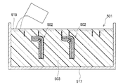
- the tactile sensor 501 includes a plurality of piezoresistive cantilevers 502 (cantilevers having piezoresistors in their hinges) formed of a thin film of about several hundreds of nanometers. It has a configuration arranged in the body 503.
- the cantilever 502 has one end formed as a fixed portion and the other end formed as a movable portion that can be deformed only in the thickness direction of the thin film forming the cantilever 502.
- Each cantilever 502 is electrically connected to a control device (not shown) through a terminal portion (not shown) and wiring. For example, when a shearing force or pressure is applied to the surface of the film-like elastic body 503, the shearing stress or compressive stress generated inside the film-like elastic body 503 operates and deforms the movable part of the cantilever 502, thereby Force or pressure can be detected.
- each cantilever 502 has, for example, the illustrated X-axis direction, Y-axis direction so that the deformation direction of the movable part is different. It arrange
- transformation direction may be arrange
- Such a film-like elastic body 503 is made of, for example, PDMS (Polydimethylsiloxane) as a material that can be easily elastically deformed by applying an external force.
- PDMS Polydimethylsiloxane
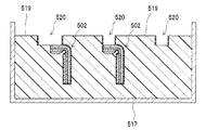
- an SOI wafer 510 on which two cantilevers 502 are formed is placed in a container 517 in a state where it is supported by a spacer 516 formed by PDMS. Thereafter, as shown in FIG. 9, the elastic body PDMS 519 in a fluid state is injected into the container 517. The implantation of the PDMS 519 is performed so that at least the cantilever 502 and the fixed portion of the cantilever 502 to the SOI wafer 510 are immersed and buried in the implanted PDMS 519.
- the partial removal of the parylene layer 518 which is a strength reinforcing member attached to the surface of the SOI wafer 510 exposed from the PDMS 519, is performed, for example, by O 2 Performed by plasma etching.
- an etching process is performed from the upper surface of the container 517 to remove the Si 511 and the SiO 2 layer 512 which are sacrificial layers of the SOI wafer 510 exposed from the PDMS 519.
- the fixed portion of each cantilever 502 to the SOI wafer 510 is removed, and each recess 520 is formed on the surface of the PDMS 519. Accordingly, by removing the sacrificial layer that has fixed the respective cantilevers 2, the individual cantilevers 502 are arranged independently of each other in the PDMS 519.
- the PDMS 519 in a fluidized state is injected into the respective recesses 520 formed on the surface of the PDMS 519 to replenish the PDMS 519.
- the injected PDMS 519 is cured to form a film-like elastic body 503 formed by PDMS, and the tactile sensor 501 is completed.
- the tactile sensor 501 having such a structure employs a manufacturing method in which the cantilever 502 formed on the SOI wafer 510 is disposed in the PDMS 519 and then the sacrificial layer that is a fixed portion to the SOI wafer 510 is removed. Therefore, the formation position of each cantilever 502 on the SOI wafer 510 becomes the formation position of each cantilever 502 in the touch sensor 501 as it is. Therefore, for example, there is a problem that it is difficult to form the tactile sensor 501 using the sheet-like film-like elastic body 503 having a large area.
- the cantilever 502 that is a minute structure may be damaged. It is possible that the handling becomes difficult.
- an object of the present invention is to solve the above-described problem, and a three-dimensional structure in which a micro three-dimensional structure element having a movable structure formed by using a MEMS technique or a NEMS technique is arranged in a film-like elastic body.
- a three-dimensional structure structure that can meet various specifications by arranging a minute three-dimensional structure element at a desired position in the structure, and that can be easily handled in its manufacture.
- An object is to provide an element, a three-dimensional structure, and a method of manufacturing the same.
- the present invention is configured as follows.
- a micro three-dimensional structure element having a movable structure; A substrate member on which the micro three-dimensional structure element is fixed; An elastic body that arranges the minute three-dimensional structure element therein, The substrate member has an engaging portion having a concave shape or a convex shape, and the elastic body is fixed to the substrate member in a state of being engaged with the engaging portion.
- An element is provided.
- a plurality of engagement hole portions are formed as the engagement portions around the fixed position of the minute three-dimensional structure element in the substrate member, and the plurality of engagement hole portions are formed in the plurality of engagement hole portions.
- the movable structure is a structure that is substantially deformable in one direction, A plurality of the micro three-dimensional structure elements having different deformable directions are arranged inside one elastic body in a state of being fixed to one substrate member.
- An element for constructing a three-dimensional structure according to an aspect is provided.
- the substrate member has a common circuit section for transferring an electric signal to and from each of the minute three-dimensional structure elements, and the three-dimensional structure according to the third aspect.
- a body constituting element is provided.
- a plurality of three-dimensional structure constituting elements according to any one of the first to fourth aspects;
- a three-dimensional structure including a plurality of three-dimensional structure constructing elements and a film-like elastic body arranged inside the substrate members in a state where the substrate members are separated from each other.
- the resin forming the elastic body has higher fluidity in its molten state than the resin forming the film-like elastic body, and the three-dimensional according to the fifth aspect. Provide a structure.
- a seventh aspect of the present invention further comprising a flexible substrate on which the plurality of three-dimensional structure constituting elements are mounted,
- the said flexible substrate provides the three-dimensional structure as described in a 5th aspect or a 6th aspect arrange
- a plurality of minute three-dimensional structure elements having a movable structure fixed to the substrate member are disposed inside the elastic body, and a concave or convex shape formed on the substrate member. Fixing the elastic body to the substrate member while engaging the engaging portion having the elastic body and the elastic body, Thereafter, the substrate member and the elastic body are cut to divide the plurality of minute three-dimensional structure elements, and one or more minute three-dimensional structure elements are fixed to the divided substrate member, Also provided is a method for manufacturing a three-dimensional structure constituting element which forms a plurality of three-dimensional structure constituting elements arranged in the divided elastic body.
- the manufacturing method of the three-dimensional structure constituent element according to the eighth aspect in which the elastic body formed of the resin material is fixed to the substrate member by curing the resin material.
- the plurality of three-dimensional structure constituting elements manufactured by the manufacturing method according to the eighth aspect or the ninth aspect are film-like elastic with the substrate members separated from each other.
- a method for manufacturing a three-dimensional structure which is arranged inside a body to form a three-dimensional structure.
- the resin forming the elastic body has higher fluidity in its molten state than the resin forming the film-like elastic body, according to the tenth aspect.
- a method for manufacturing a structure is provided.
- a plurality of three-dimensional structure constituting elements having an elastic body fixed to the substrate member and disposed inside the small three-dimensional structure element fixed to the substrate member,
- a three-dimensional structure is formed by arranging the substrate members in a film-like elastic body in a state where the substrate members are separated from each other. Therefore, it is possible to arrange a plurality of three-dimensional structure constituting elements in a film-like elastic body at desired arrangement intervals and positions, and to provide a three-dimensional structure that can correspond to various specifications. Can do.
- a three-dimensional structure constituting element of the present invention after covering a plurality of minute three-dimensional structure elements formed on the substrate member with an elastic body, the substrate member and the elastic body are bonded together.
- the substrate member and the elastic body are bonded together.
- one or a plurality of minute three-dimensional structure elements can be divided to form a plurality of three-dimensional structure constituting elements.
- each micro three-dimensional structure element is covered and protected by an elastic body, so that the micro three-dimensional structure element can be prevented from being damaged and divided.
- the handleability of the formed three-dimensional structure constituting element can be improved.
- the engaging portion provided on the board member and the elastic body are engaged, whereby the elastic body is fixed to the board member, so that the strength in this fixing can be increased. Therefore, in the element for constituting a three-dimensional structure, the unity between the movable structure of the minute three-dimensional structure element and the elastic body can be enhanced, and the relationship between the operation of the movable structure and the deformation of the elastic body can be strengthened. it can.
- It is a schematic diagram of a manufacturing method of a sensor element is a diagram of a state in which a substrate member is formed
- It is a schematic diagram of a manufacturing method of a sensor element is a diagram in a state in which a hole for engagement is formed in a substrate member
- It is a schematic diagram of the manufacturing method of the sensor element is a diagram in a state where the cantilever is formed
- It is a schematic diagram of a manufacturing method of a sensor element is a diagram of a state in which an elastic body is arranged
- It is a schematic diagram of the manufacturing method of the sensor element is a diagram of a state in which the sensor element is divided
- It is another schematic diagram showing a manufacturing method of the sensor element is a diagram in a state where a cantilever is formed
- It is another schematic diagram showing the manufacturing method of the sensor element is a diagram in a state of supplying an elastic body
- It is another schematic diagram showing the manufacturing method of the sensor element is a diagram in a state where the
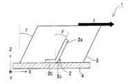
- FIG. 1 is a schematic diagram of a sensor element 1 which is an example of a three-dimensional structure constituting element used for constituting a tactile sensor (or a tactile sensor structure) which is an example of a three-dimensional structure according to an embodiment of the present invention.
- a schematic perspective view showing a simple structure is shown in FIG.
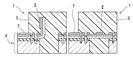
- the sensor element 1 of the present embodiment includes a plurality of cantilevers 2 that are examples of a micro three-dimensional structure element having a movable structure, and a substrate member 4 to which the plurality of cantilevers 2 are fixed, And an elastic body 3 fixed on the substrate member 4 so as to cover the entire cantilever 2.
- each cantilever 2 is formed in a thin film shape with a thickness of, for example, about several hundred nm, and one end (fixed end) thereof is fixed to the fixed portion 2b. And the other end (free end) as a movable portion 2a, and a movable structure, that is, a cantilever structure.
- the cantilever 2 is formed so that the thickness dimension is sufficiently thin with respect to the width direction, and the movable portion 2a can be deformed in the thickness direction with respect to the fixed portion 2b.
- each cantilever 2 is provided with a hinge portion 2c that is an example of a connecting portion that connects the movable portion 2a and the fixed portion 2b, and the movable portion 2a operates by deformation thereof, and this hinge portion 2c.
- the sensor element 1 is provided with three types of cantilevers 2 having different directions of deformation of the movable portion 2a.
- An axial cantilever 2X, a Y-axis cantilever 2Y whose deformation direction is the Y-axis direction in the figure, and a Z-axis cantilever 2Z whose deformation direction is the Z-axis direction in the figure are provided.
- an X-axis direction and a Y-axis direction are directions orthogonal to each other along the surface of the substrate member 4, and a direction orthogonal to the X-axis direction and the Y-axis direction is a Z-axis direction.
- the elastic body 3 is formed of an elastic material having such flexibility that the elastic body 3 is elastically deformed by the application of an external force or the like, and the elastic deformation operates (deforms) the movable portion 2a of the cantilever 2.
- transparent or colored PDMS Polydimethylsiloxane
- the elastic body 3 also has a function of protecting each cantilever 2 from being damaged by direct contact with an external object or the like, and has a thickness that covers the entire cantilever 2.
- the thickness dimension is, for example, about 300 ⁇ m to 1 mm or less, and can achieve both flexibility and strength while effectively achieving the stress detection function of the cantilever 2 described later. It is more desirable to be formed.
- a through opening 5 is formed for each cantilever 2 at the formation position of each cantilever 2 in the substrate member 4, and the cantilever 2 is fixed to the edge of the through opening 5.
- the part 2b is fixed.
- the through openings 5 are formed in a size that does not interfere with the movable part 2 a of the cantilever 2 at the edge of each through opening 5.
- terminal portions are provided in the fixed portions 2 b of the respective cantilevers 2, and wirings 6 are individually provided in these terminal portions, and the movable portions in the respective cantilevers 2. It is possible to electrically detect the operation angle 2a.
- the sensor element 1 is provided with a circuit unit (control circuit or the like, not shown) that exchanges electric signals with each cantilever 2 through the wiring 6.
- electrode terminals 7 to which respective wirings 6 are connected are provided at both ends of the substrate member 4 in the Y-axis direction in the figure.
- the elastic body 3 is disposed so as to expose each electrode terminal 7 and completely cover each through-opening 5 and the entire cantilever 2.
- the electrode terminal 7 is exposed on the upper surface of the substrate member 4, but the electrode terminal 7 may be exposed on the rear surface of the substrate member 4.
- the electrode terminal 7 is electrically connected to the wiring 6 by a conductor or the like penetrating the substrate member 4.
- a large number of engagement hole portions 8, which are examples of engagement portions, are formed on the upper surface of the substrate member 4 around each through opening 5.
- the engagement hole 8 is filled with the elastic body 3, and the engagement between the engagement hole 8 and the elastic body 3 filled inside thereof causes the elastic body 3, the substrate member 4, and the like. Are firmly engaged and fixed.
- the elastic body 3 has a high fluidity (e.g., before hardening) that can easily enter a nanoscale structure (hole portion or the like). It is preferred to use a material having (in the molten state).
- a product called Sylgard184 manufactured by DowCorning which is used for mold making / transfer of a nanoscale structure can be used.
- the movable part 2 a having a shearing direction or a compressive stress generated in the elastic body 3 as a deformation direction.
- the movable part 2a of the cantilever 2 that is provided can be detected by being deformed.
- the X-axis direction cantilever 2X and the Y-axis direction cantilever 2Y in FIG. 1 function as a shear force sensor that detects a force (shear force) generated in a direction along the surface of the film-like elastic body 3, and is in the Z-axis direction.
- the cantilever 2Z functions as a pressure sensor that detects a force in the Z-axis direction of the film-like elastic body 3, that is, a compressive stress.
- the cantilever 2Z for the Z-axis direction may be formed in a cantilever shape similarly to the cantilevers 2X and 2Y, or instead of such a case. Further, it may be a case where the both ends are formed in a doubly supported beam shape that is fixed to the substrate member 4.
- the hinge part 2c of the cantilever 2 is provided with a piezoresistive part.
- the piezoresistive portion has a function of changing its electrical resistance value according to the deformation amount of the movable portion 2a, and the correlation between the deformation amount and the resistance value is measured in advance, The correlation data is input and held in a control device (not shown) connected to the electrode terminal 7. Accordingly, by detecting a change in resistance of the piezoresistive portion based on the amount of shear strain ⁇ generated in the elastic body 3 by the shear stress ⁇ deforming the cantilever 2, the shear stress ⁇ generated in the elastic body 3 due to the external force action is detected. Can be detected.
- the movable portion in the X-axis direction cantilever 2X and the Y-axis direction cantilever 2Y that detects the force in the direction along the surface of the elastic body 3 is used.
- the tactile sensor 10 has a plurality of sensor elements 1 arranged therein so as to cover the flexible substrate 11 mounted in a predetermined position and the sensor element 1 and the flexible substrate 11 as a whole.
- the film-like elastic body 12 is provided.
- the flexible substrate 11 has high flexibility, and wirings 13 for transmitting signals to and from each mounted sensor element are formed.
- the wiring 13 is connected to the electrode terminal 7 exposed on the upper surface of the substrate member 4 of the sensor element 1 via a conductor wire, or is exposed on the back surface of the substrate member 4 of the sensor element 1.
- the electrode terminal 7 is directly connected.
- the sensor elements 1 are mounted at predetermined positions so as not to contact each other, for example, the substrate members 4 are separated from each other.
- the film-like elastic body 12 is made of an elastic material having high flexibility, and for example, PDMS is used as such an elastic material.
- the tactile sensor 10 of this embodiment has such a configuration, the tactile sensor 10 has high flexibility and is arranged on a surface having various shapes, for example, a curved surface, as shown in the schematic diagram of FIG. Thus, an external force (shearing force or pressure) applied to the film-like elastic body 12 can be detected.
- FIGS. 5A to 5E are schematic cross-sectional views showing the procedure of the manufacturing method of the sensor element 1
- FIGS. 6A to 6D are schematic perspective views showing the state of the sensor element 1 in each step. Show.
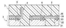
- a rapid thermal diffusion is performed using, for example, an SOI wafer 20 composed of a 300 ⁇ m thick Si lower layer 21, a 400 nm thick SiO 2 layer 22 and a 290 nm thick Si upper layer 23.
- the upper 100 nm portion of the Si upper layer 23 is formed as a piezoresistive layer (part) 24, and then an Au / Ni layer 25 having a thickness of 10 nm and 150 nm is sputtered on the piezoresistive layer 24, respectively. Etc. are formed.
- the SOI wafer 20 finally becomes the substrate member 4.
- a plurality of engagement holes 8 are formed around the formation position of the cantilever 2 from the Au / Ni layer 25 side. Specifically, after a mask layer (not shown) patterned in a predetermined shape is formed on the Au / Ni layer 25, the Au / Ni layer 25 is etched, and the piezoresistive layer 24 and the Si upper layer 23 are further formed. Etching is performed by DRIE (Deep Reactive Ion Etching). Thereafter, the SiO 2 layer 22 is etched using an HF (hydrogen fluoride) solution, and the Si lower layer 21 is further etched by DRIE. By this etching process, a plurality of engagement holes 8 are formed on the SOI wafer 20 as shown in FIG. 5B.
- DRIE Deep Reactive Ion Etching
- the engagement hole 8 is preferably formed in the vicinity of the position where the cantilever 2 is to be formed later, and at a position where it does not interfere with other components such as the wiring 6 at a depth of, for example, about 40 ⁇ m. It is formed. Further, after the etching process is completed, the mask layer is removed.
- a mask layer (not shown) is formed on the Au / Ni layer 25 in which the plurality of engagement holes 8 are formed, and then patterned into a predetermined shape. Etching is performed on the Au / Ni layer 25, the piezoresistive layer 24, and the Si upper layer 23. Thereafter, in order to form the piezoresistive portion of the cantilever 2, the mask layer disposed so as to cover the portion corresponding to the hinge portion that connects the fixed portion 2b and the movable portion 2a of the cantilever 2 is removed by etching. To do.
- the Si lower layer 21 is etched by DRIE, and further, the SiO 2 layer is etched using HF gas, whereby the movable part 2a, that is, the free end of the cantilever 2 is obtained.
- the structure portion to be formed is opened from the Si lower layer 21 and the SiO 2 layer (that is, the through opening 5 is formed).
- the basic structure as the cantilever 2 is completed.
- the movable portions 2a of the X-axis direction and Y-axis direction cantilevers 2X and 2Y are raised along the vertical direction, and a predetermined process is performed.
- the state where the movable part 2a is raised (the standing posture state) is held.
- the movable portion 2a of the cantilever 2Z for the Z-axis direction is not raised, and the horizontal posture is maintained.
- FIGS. 5C and 6A a plurality of cantilevers 2 fixed to the substrate member 4 with the SOI wafer 20 as a base are formed.
- FIG. 5C only two cantilevers 2, for example, an X-axis direction cantilever 2 ⁇ / b> X and a Z-axis direction cantilever 2 ⁇ / b> Z are illustrated as the cantilever 2.
- FIG. 7 shows the cantilever 2 in a state before the standing posture.
- the cantilever 2 has, for example, a width dimension d1 of the movable part 2a of 80 ⁇ m, a length dimension d2 of the movable part 2a of 200 ⁇ m, and the length of the hinge part 2c between the movable part 2a and the fixed part 2b.
- the length d3 is 100 ⁇ m
- the width of each hinge portion 2c is 25 ⁇ m
- the overall length of the cantilever 2 is 300 ⁇ m.
- the thickness dimension of the piezoresistive layer 24 is 100 nm.
- a terminal portion 9 for exchanging electrical signals with the outside is formed on the fixing portion 2 b of the cantilever 2.
- the hinge part 2c between the movable part 2a and the fixed part 2b is provided with a hollow part in the plan view.
- an output such as an inclination given to each structure can be output to each piezoresistor.
- the width dimension of the said structure in such a hinge part 2c is formed in 25 micrometers, for example.
- micro of a micro three-dimensional structure element refers to, for example, a plurality of three-dimensional structure elements (that is, cantilevers 2) in an elastic body 3 formed to a thickness of about 100 ⁇ m to 1 mm.
- the elastic body 3 is formed so as to cover each cantilever 2 formed on the SOI wafer 20 as described above.
- a fluidized (or molten) elastic body (for example, PDMS for nanostructure described above) 3 is injected and supplied to the surface of the SOI wafer 20 on the side where the cantilever 2 is formed.
- the elastic body 3 is supplied in such a manner that at least all the cantilevers 2 are immersed and embedded in the elastic body 3.
- the elastic body 3 since the elastic body 3 has high fluidity, the elastic body 3 is also injected and filled into the respective through openings 5 and the engagement holes 8.
- each cantilever 2 is disposed inside the elastic body 3 as shown in FIGS. 5D and 6C. Further, in this state, since the elastic body 3 enters and hardens into the respective engagement holes 8, the elastic body 3 and the surface of the substrate member 4 are firmly engaged with each other. It is fixed.
- the elastic body 3 is formed with a thickness of, for example, 500 ⁇ m.
- the plurality of sensor elements 1 are in a state in which the substrate member 4 and the elastic body 3 are integrally connected. Thereafter, as shown in FIG. 6D, the elastic body 3 and the substrate member 4 are cut using a dicer 29 which is an example of a cutting jig. As a result, as shown in FIG. 5E, the sensor elements 1 are divided from each other to form a plurality of sensor elements 1. In addition, before and after the division of the sensor element 1, that is, before and after the dicing process, the elastic body 3 disposed on the electrode terminal 7 of the sensor element 1 is partially removed, and the process of exposing the electrode terminal 7 is performed. Is called. For example, as shown in FIG.
- the sensor element 1 thus formed includes an X-axis direction cantilever 2 ⁇ / b> X, a Y-axis direction cantilever 2 ⁇ / b> Y, and a Z-axis direction cantilever 2 ⁇ / b> Z. It is formed with a size of 2 mm and about 2 mm in the Y-axis direction.
- each sensor element 1 is mounted at a predetermined mounting position on the flexible substrate 11.
- the flexible substrate 11 on which the plurality of sensor elements 1 are mounted is placed in the film-like elastic body 12 by immersing it in the PDMS in a fluid state.
- the tactile sensor 10 shown in FIG. 3 is completed.
- each sensor element 1 is arranged so that the hinge part 2c of each cantilever 2 is positioned on the neutral line of the film-like elastic body 12 in the thickness direction of the touch sensor 10.
- the film-like elastic body 12 is formed by supplying PDMS in a fluidized state
- the two films are sandwiched by sandwiching the flexible substrate 11 using the two film-like PDMS. It may be a case where it is performed by bonding to a metal.
- each sensor element 1 and the flexible substrate 11 are both arranged inside the film-like elastic body 12
- each sensor element 1 is arranged inside the film-like elastic body 12
- a structure in which the flexible substrate 11 is disposed so as to be in contact with the film-like elastic body 11 can also be adopted.
- each sensor element 1 is arranged in the film-like elastic body 12 by, for example, transferring PDMS to the surface of the flexible substrate 11 on which the sensor element 1 is mounted. Techniques can also be adopted.
- the cantilever 2 which is such a minute three-dimensional structure element has a movable structure in which at least a part of the cantilever 2 is movable.
- This is a structural element having a structure that can move with the elastic body.
- the three-dimensional structure constituent element (sensor element 1) formed by embedding such a micro three-dimensional structure element in the elastic body is used for a sensor or the like that detects deformation of the movable portion (movable structure).
- each micro three-dimensional structure element is movable. It may be a case where it does not have a structure, and the manufacturing method of the present invention can be applied to manufacture a three-dimensional structure constituting element.
- the micro three-dimensional structure element has an external force detection function for detecting the operation (deformation) of the movable structure based on the elastic deformation (for example, shear strain) generated in the elastic body by the action of the external force on the three-dimensional structure.
- the movable structure is operated (deformed) so that an external force is transmitted to an elastic body arranged around the movable structure and the elastic structure is elastically deformed. May be.
- Such an external force detection function is represented by a function as a tactile sensor, for example, taking a cantilever as an example, and the external force transmission function partially elastically deforms an elastic body by operating the cantilever as an actuator. It is a function like this.
- the function can be exhibited individually and reliably in a state of being embedded in the elastic body.
- the piezoresistive layer (part) in the cantilever is an external force detection unit having such a function.
- the cantilever can also function as an external force transmission unit.
- a mechanism for operating the movable unit for example, a piezoelectric element is separately provided, or a magnetic field is applied using magnetic anisotropy to operate the movable unit. be able to.
- the external force detection function can be used to detect the external force and transmit the information using the external force transmission function.
- the three-dimensional structure constituting element and the three-dimensional structure can be applied to an integrated circuit, a display (organic EL), etc. in addition to being applied as a sensor or an actuator in this way.
- a tactile sensor measures the shape of an object surface by bringing a film-like elastic body into contact with the surface of an object having a large area (particularly having a curved shape).
- the present invention can also be applied to measuring instrument probes, computer input pointing devices, tablets, and input and output devices for realizing virtual reality.
- the three-dimensional structure can also be configured as a temperature sensor or an acceleration sensor that allows a minute three-dimensional structure element having a movable structure to function as a structure element that detects temperature and acceleration.
- a temperature compensation sensor is configured by integrally configuring a sensor by mixing a micro three-dimensional structure element having a temperature detection function and a micro three-dimensional structure element having other functions in an elastic body. Can also be configured.
- a film-like elastic body 12 is used.
- the tactile sensor 10 can be configured by arranging the sensor elements 1 in a state of being separated from each other. Therefore, a plurality of sensor elements 1 can be arranged at desired arrangement intervals and positions in the film-like elastic body 12, and the tactile sensor 10 that can correspond to various uses and specifications can be provided.
- the arrangement of each cantilever is as follows. Since the interval and position are limited to the formation position on the SOI wafer, there is a problem that the degree of freedom of arrangement of the cantilever 2 is low. However, as in this embodiment, the plurality of cantilevers 2 formed on the SOI wafer 20 are divided into one or a plurality of groups, and the divided individual cantilevers 2 are separated into desired arrangement intervals and It can arrange
- the tactile sensor 10 having a sheet-like form with a large area.
- it can be dealt with by simply changing the arrangement interval of the sensor element 1 without changing the design from the mask layout used in the etching process.
- the degree of freedom of arrangement of the cantilever 2 can be increased.
- each cantilever 2 formed on the SOI wafer 20 is covered with the elastic body 3, the SOI wafer 20 and the elastic body 3 are cut and the individual sensor elements 1 are separated.
- a method of dividing is employed.
- each cantilever 2 can be protected by the elastic body 3 even in the sensor element 1 after being divided.
- such a cantilever 2 itself is a minute structural element formed by MEMS or NEMS technology, and thus has a characteristic that it is relatively easily damaged.
- the cantilever 2 can be reliably protected during the division process.
- the state where the cantilever 2 is protected by the elastic body 3 is continued even in the individual sensor elements 1, the protection of the cantilever 2 is ensured.
- a plurality of engagement holes 8 are formed around the positions where the cantilevers 2 are formed on the surface of the substrate member 4, and the elastic body 3 is placed inside the engagement holes 8.
- the strength of fixing the elastic body 3 to the substrate member 4 can be increased.
- durability of the sensor element 1 can be improved by improving the fixing strength.
- by providing such an engagement hole 8 around the cantilever 2 having the movable portion 2a the integrity of the cantilever 2 and the elastic body 3 in the vicinity thereof can be improved.
- the relationship between the operation 2a and the deformation of the elastic body 3 can be strengthened.
- the tactile sensor 10 employs a configuration in which two elastic bodies, that is, the film-like elastic body 12 and the elastic body 3 of the sensor element 1 are used. And can vary depending on the function. For example, by using an elastic material having higher fluidity than the film-like elastic body 12 as the elastic body 3, various constituent parts (cantilever 2 and engagement hole 8) having a minute shape formed on the substrate member 4 are used. The elastic body 3 can be inserted into the details, and the elastic body 3 can be disposed so as to be surely in contact with the surface of each component. On the other hand, as the film-like elastic body 12, an elastic material having specifications corresponding to the application and specifications of the touch sensor 10 can be used.
- the tactile sensor 10 that can respond to various specifications and applications while ensuring the function as the sensor element 1.
- the same type of elastic material may be used for the film-like elastic body 12 and the elastic body 3.
- the thickness of the elastic body 3 of the sensor element 1 can be set according to the application and specification of the touch sensor 10. For example, by setting the thickness of the elastic body 3 to be thick, the amount of displacement of the elastic body 3 becomes large even when the same magnitude force (shearing force or pressure) is applied, so that the object touching the touch sensor 10 is soft. You can touch. In addition, since the applied force is dispersed, the cantilever 2 and the like can be prevented from being damaged. Moreover, the frequency characteristics of stress detection tend to decrease as the thickness of the elastic body 3 increases. Therefore, it is preferable to set the thickness of the elastic body 3 of the sensor element 1 according to the required specification of the tactile sensor 10.
- a quality inspection can be performed on the sensor element 1 alone.
- the defective sensor element 1 can be eliminated and the tactile sensor 10 can be manufactured, and the quality of the manufactured tactile sensor 10 can be improved.
- the cantilever 2 capable of detecting stress in three different directions of the X-axis direction cantilever 2X, the Y-axis direction cantilever 2Y, and the Z-axis direction cantilever 2Z is disposed in the sensor element 1.
- the present embodiment is not limited to such a case. Instead of such a case, for example, only one cantilever 2 may be provided in the sensor element 1, or a plurality of cantilevers 2 capable of detecting stress in the same direction are provided. But you can.
- the one sensor element 1 that is, the same It is possible to detect stress in three directions different in position.
- the circuit unit included in the sensor element 1 has a specification that can be adjusted for each sensor element 1 by sharing a circuit common to such three cantilevers 2, for example, a control circuit such as temperature compensation and amplification. The reliability of the sensor element 1 can be improved.
- sharing the circuit part as described above it is possible to share the electrical conditions of the sensor element 1 and to reduce the size of the circuit configuration.
- the engagement hole 8 is formed as a hole that does not penetrate the substrate member 4 .
- the engagement hole 8 is formed as a through hole. You can also When formed as a through hole, the filling property of the elastic body 3 into the engagement hole 8 can be improved. On the other hand, when it is formed as a hole that does not penetrate, the filling property can be enhanced by vacuum degassing bubbles remaining in the hole using an elastic material having high fluidity.
- the engagement hole 8 is preferably formed so as to increase the surface area of contact with the elastic body 3 in the substrate member 4, and the engagement hole 8 having a small hole diameter has a deeper depth. It is preferable to form a large number of them. Further, from the viewpoint of increasing the contact surface area, the inner surface of the hole 8 is preferably formed with a surface with many irregularities. However, considering the specifications such as the fluidity of the elastic body 3, it is desirable to determine the hole diameter, depth dimension, inner surface shape, and the like from the viewpoint of reliable filling. Further, it is desirable that the number and specifications of the engagement holes 8 are determined so as not to impair the strength of the board member 4.
- the engaging hole 8 has been described as an example of the engaging portion.
- the hole 8 has various shapes such as an ellipse, a rectangle, and a polygon in addition to a circle. can do.
- substrate member 4 as an engaging part may be sufficient.
Landscapes
- Physics & Mathematics (AREA)
- General Physics & Mathematics (AREA)
- Chemical & Material Sciences (AREA)
- Analytical Chemistry (AREA)
- Engineering & Computer Science (AREA)
- Computer Hardware Design (AREA)
- Microelectronics & Electronic Packaging (AREA)
- Force Measurement Appropriate To Specific Purposes (AREA)
- Micromachines (AREA)
- Pressure Sensors (AREA)
Priority Applications (2)
| Application Number | Priority Date | Filing Date | Title |
|---|---|---|---|
| US12/920,147 US8482086B2 (en) | 2008-03-13 | 2009-03-13 | Three-dimensional structure and its manufacturing method |
| CN2009801072470A CN101960275A (zh) | 2008-03-13 | 2009-03-13 | 三维结构体及其制造方法 |
Applications Claiming Priority (2)
| Application Number | Priority Date | Filing Date | Title |
|---|---|---|---|
| JP2008-064359 | 2008-03-13 | ||
| JP2008064359A JP4508253B2 (ja) | 2008-03-13 | 2008-03-13 | 3次元構造体およびその製造方法 |
Publications (1)
| Publication Number | Publication Date |
|---|---|
| WO2009113315A1 true WO2009113315A1 (ja) | 2009-09-17 |
Family
ID=41064988
Family Applications (1)
| Application Number | Title | Priority Date | Filing Date |
|---|---|---|---|
| PCT/JP2009/001126 Ceased WO2009113315A1 (ja) | 2008-03-13 | 2009-03-13 | 3次元構造体およびその製造方法 |
Country Status (4)
| Country | Link |
|---|---|
| US (1) | US8482086B2 (enExample) |
| JP (1) | JP4508253B2 (enExample) |
| CN (1) | CN101960275A (enExample) |
| WO (1) | WO2009113315A1 (enExample) |
Families Citing this family (7)
| Publication number | Priority date | Publication date | Assignee | Title |
|---|---|---|---|---|
| JP5198608B2 (ja) * | 2010-03-18 | 2013-05-15 | 韓国標準科学研究院 | 半導体ストレインゲージを用いたフレキシブルな力または圧力センサアレイ、そのフレキシブルな力または圧力センサアレイの製造方法、及びそのフレキシブルな力または圧力センサアレイを用いた力または圧力測定方法 |
| JP2013090498A (ja) * | 2011-10-20 | 2013-05-13 | Sumitomo Precision Prod Co Ltd | アクチュエータ及びその製造方法 |
| CN104321613B (zh) | 2012-05-24 | 2017-03-29 | 株式会社村田制作所 | 传感器装置以及电子设备 |
| DE202013101814U1 (de) * | 2013-04-26 | 2014-07-29 | Zumtobel Lighting Gmbh | LED-Modul mit Berührungsschutzelement |
| US10628103B2 (en) | 2013-06-07 | 2020-04-21 | Semiconductor Energy Laboratory Co., Ltd. | Information processor and program |
| CN110023730B (zh) * | 2016-11-24 | 2021-11-09 | 昆士兰大学 | 力感测装置 |
| US10512164B2 (en) * | 2017-10-02 | 2019-12-17 | Encite Llc | Micro devices formed by flex circuit substrates |
Citations (5)
| Publication number | Priority date | Publication date | Assignee | Title |
|---|---|---|---|---|
| JPH02641Y2 (enExample) * | 1988-07-26 | 1990-01-09 | ||
| JP2000065653A (ja) * | 1998-08-26 | 2000-03-03 | Asmo Co Ltd | 固定構造、感圧センサ固定方法、及び圧力検出装置 |
| JP2006208248A (ja) * | 2005-01-28 | 2006-08-10 | Univ Of Tokyo | 触覚センサ及びその製造方法 |
| JP2006275979A (ja) * | 2005-03-30 | 2006-10-12 | National Institute Of Information & Communication Technology | センサ素子、センサ装置、対象物移動制御装置、対象物判別装置 |
| JP2008026178A (ja) * | 2006-07-21 | 2008-02-07 | Advanced Telecommunication Research Institute International | 触覚センサ装置 |
Family Cites Families (15)
| Publication number | Priority date | Publication date | Assignee | Title |
|---|---|---|---|---|
| US4814392A (en) | 1987-11-25 | 1989-03-21 | General Electric Company | Silicone-polyarylene ether block copolymers, and method for making |
| US5101669A (en) * | 1988-07-14 | 1992-04-07 | University Of Hawaii | Multidimensional force sensor |
| JP2804196B2 (ja) * | 1991-10-18 | 1998-09-24 | 株式会社日立製作所 | マイクロセンサ及びそれを用いた制御システム |
| US6316796B1 (en) * | 1995-05-24 | 2001-11-13 | Lucas Novasensor | Single crystal silicon sensor with high aspect ratio and curvilinear structures |
| JP2002118201A (ja) * | 2000-10-05 | 2002-04-19 | Hitachi Ltd | 半導体装置およびその製造方法 |
| JP3704558B2 (ja) | 2002-01-18 | 2005-10-12 | 国立大学法人 東京大学 | 3次元構造体の組立方法 |
| US7357035B2 (en) * | 2003-06-06 | 2008-04-15 | The Board Of Trustees Of The University Of Illinois | Sensor chip and apparatus for tactile and/or flow sensing |
| JP2005150220A (ja) * | 2003-11-12 | 2005-06-09 | Seiko Epson Corp | 半導体装置、半導体ウエハおよびその製造方法 |
| US20050172717A1 (en) * | 2004-02-06 | 2005-08-11 | General Electric Company | Micromechanical device with thinned cantilever structure and related methods |
| US7032454B2 (en) * | 2004-03-05 | 2006-04-25 | Agilent Technologies, Inc. | Piezoelectric cantilever pressure sensor array |
| JP4921185B2 (ja) * | 2006-01-20 | 2012-04-25 | 国立大学法人 東京大学 | 3次元構造体の製造方法 |
| US7825567B2 (en) * | 2006-01-20 | 2010-11-02 | Panasonic Corporation | Three-dimensional structure and its manufacturing method |
| JP2008008854A (ja) | 2006-06-30 | 2008-01-17 | Osaka Univ | 触覚センサ、触覚センサの製造方法および触覚センサユニット |
| JP2008044219A (ja) * | 2006-08-15 | 2008-02-28 | Fuji Xerox Co Ltd | 基板の製造方法と基板、及び液滴吐出ヘッドの製造方法と液滴吐出ヘッド、並びに液滴吐出装置 |
| JP2008049438A (ja) | 2006-08-24 | 2008-03-06 | Osaka Univ | 半導体装置の製造方法、半導体装置、及び感圧センサ |
-
2008
- 2008-03-13 JP JP2008064359A patent/JP4508253B2/ja not_active Expired - Fee Related
-
2009
- 2009-03-13 US US12/920,147 patent/US8482086B2/en not_active Expired - Fee Related
- 2009-03-13 CN CN2009801072470A patent/CN101960275A/zh active Pending
- 2009-03-13 WO PCT/JP2009/001126 patent/WO2009113315A1/ja not_active Ceased
Patent Citations (5)
| Publication number | Priority date | Publication date | Assignee | Title |
|---|---|---|---|---|
| JPH02641Y2 (enExample) * | 1988-07-26 | 1990-01-09 | ||
| JP2000065653A (ja) * | 1998-08-26 | 2000-03-03 | Asmo Co Ltd | 固定構造、感圧センサ固定方法、及び圧力検出装置 |
| JP2006208248A (ja) * | 2005-01-28 | 2006-08-10 | Univ Of Tokyo | 触覚センサ及びその製造方法 |
| JP2006275979A (ja) * | 2005-03-30 | 2006-10-12 | National Institute Of Information & Communication Technology | センサ素子、センサ装置、対象物移動制御装置、対象物判別装置 |
| JP2008026178A (ja) * | 2006-07-21 | 2008-02-07 | Advanced Telecommunication Research Institute International | 触覚センサ装置 |
Also Published As
| Publication number | Publication date |
|---|---|
| US8482086B2 (en) | 2013-07-09 |
| US20110006383A1 (en) | 2011-01-13 |
| JP2009222415A (ja) | 2009-10-01 |
| CN101960275A (zh) | 2011-01-26 |
| JP4508253B2 (ja) | 2010-07-21 |
Similar Documents
| Publication | Publication Date | Title |
|---|---|---|
| JP4921185B2 (ja) | 3次元構造体の製造方法 | |
| JP4508253B2 (ja) | 3次元構造体およびその製造方法 | |
| Lee et al. | Normal and shear force measurement using a flexible polymer tactile sensor with embedded multiple capacitors | |
| Thanh-Vinh et al. | High-sensitivity triaxial tactile sensor with elastic microstructures pressing on piezoresistive cantilevers | |
| US8109149B2 (en) | Contact stress sensor | |
| US8440089B2 (en) | Three-dimensional structure and its manufacturing method | |
| CN101512311B (zh) | 用于曲面的触觉传感器及其制备方法 | |
| WO2010149651A1 (en) | Optical tactile sensors | |
| JP2006208248A (ja) | 触覚センサ及びその製造方法 | |
| JP4335545B2 (ja) | 圧力と加速度との双方を検出するセンサおよびその製造方法 | |
| WO2016185813A1 (ja) | 多軸触覚センサ及び多軸触覚センサの製造法 | |
| US20170001857A1 (en) | Sensor element and method of manufacturing the same | |
| JP5647481B2 (ja) | 触覚センサユニット | |
| JP2004233072A (ja) | 加速度センサ | |
| CN100436306C (zh) | 一种触觉传感器及其制作方法 | |
| JP2008049438A (ja) | 半導体装置の製造方法、半導体装置、及び感圧センサ | |
| JP7510157B2 (ja) | センサユニットおよびセンサ | |
| JP4839826B2 (ja) | センサモジュール | |
| KR100735295B1 (ko) | 폴리머 필름을 이용한 플렉서블 촉각센서 제조방법 | |
| JP7737663B2 (ja) | Memsセンサ | |
| KR20090027941A (ko) | 촉각 센서 및 그의 제조 방법 | |
| Hou et al. | Wide range bridge type 3D tactile sensor with variable sensitivity through replaceable elastic layer attaching on PDMS cap | |
| Sato et al. | Shear force sensor using a cantilever with liquid-embedded hinges | |
| JP2007173637A (ja) | センサモジュール | |
| KR101109193B1 (ko) | 촉각 센서 어레이 및 그 제조방법 |
Legal Events
| Date | Code | Title | Description |
|---|---|---|---|
| WWE | Wipo information: entry into national phase |
Ref document number: 200980107247.0 Country of ref document: CN |
|
| 121 | Ep: the epo has been informed by wipo that ep was designated in this application |
Ref document number: 09718932 Country of ref document: EP Kind code of ref document: A1 |
|
| WWE | Wipo information: entry into national phase |
Ref document number: 12920147 Country of ref document: US |
|
| NENP | Non-entry into the national phase |
Ref country code: DE |
|
| 122 | Ep: pct application non-entry in european phase |
Ref document number: 09718932 Country of ref document: EP Kind code of ref document: A1 |