WO2009084670A1 - Semiconductor light emitting element and method for manufacturing the same - Google Patents
Semiconductor light emitting element and method for manufacturing the same Download PDFInfo
- Publication number
- WO2009084670A1 WO2009084670A1 PCT/JP2008/073821 JP2008073821W WO2009084670A1 WO 2009084670 A1 WO2009084670 A1 WO 2009084670A1 JP 2008073821 W JP2008073821 W JP 2008073821W WO 2009084670 A1 WO2009084670 A1 WO 2009084670A1
- Authority
- WO
- WIPO (PCT)
- Prior art keywords
- convex
- light emitting
- semiconductor
- emitting device
- electrode
- Prior art date
Links
Images


Classifications
-
- H—ELECTRICITY
- H01—ELECTRIC ELEMENTS
- H01L—SEMICONDUCTOR DEVICES NOT COVERED BY CLASS H10
- H01L33/00—Semiconductor devices with at least one potential-jump barrier or surface barrier specially adapted for light emission; Processes or apparatus specially adapted for the manufacture or treatment thereof or of parts thereof; Details thereof
- H01L33/005—Processes
- H01L33/0062—Processes for devices with an active region comprising only III-V compounds
- H01L33/0066—Processes for devices with an active region comprising only III-V compounds with a substrate not being a III-V compound
- H01L33/007—Processes for devices with an active region comprising only III-V compounds with a substrate not being a III-V compound comprising nitride compounds
-
- H—ELECTRICITY
- H01—ELECTRIC ELEMENTS
- H01L—SEMICONDUCTOR DEVICES NOT COVERED BY CLASS H10
- H01L33/00—Semiconductor devices with at least one potential-jump barrier or surface barrier specially adapted for light emission; Processes or apparatus specially adapted for the manufacture or treatment thereof or of parts thereof; Details thereof
- H01L33/005—Processes
- H01L33/0093—Wafer bonding; Removal of the growth substrate
-
- H—ELECTRICITY
- H01—ELECTRIC ELEMENTS
- H01L—SEMICONDUCTOR DEVICES NOT COVERED BY CLASS H10
- H01L33/00—Semiconductor devices with at least one potential-jump barrier or surface barrier specially adapted for light emission; Processes or apparatus specially adapted for the manufacture or treatment thereof or of parts thereof; Details thereof
- H01L33/02—Semiconductor devices with at least one potential-jump barrier or surface barrier specially adapted for light emission; Processes or apparatus specially adapted for the manufacture or treatment thereof or of parts thereof; Details thereof characterised by the semiconductor bodies
- H01L33/20—Semiconductor devices with at least one potential-jump barrier or surface barrier specially adapted for light emission; Processes or apparatus specially adapted for the manufacture or treatment thereof or of parts thereof; Details thereof characterised by the semiconductor bodies with a particular shape, e.g. curved or truncated substrate
- H01L33/22—Roughened surfaces, e.g. at the interface between epitaxial layers
-
- H—ELECTRICITY
- H01—ELECTRIC ELEMENTS
- H01L—SEMICONDUCTOR DEVICES NOT COVERED BY CLASS H10
- H01L2933/00—Details relating to devices covered by the group H01L33/00 but not provided for in its subgroups
- H01L2933/0008—Processes
- H01L2933/0016—Processes relating to electrodes
-
- H—ELECTRICITY
- H01—ELECTRIC ELEMENTS
- H01L—SEMICONDUCTOR DEVICES NOT COVERED BY CLASS H10
- H01L2933/00—Details relating to devices covered by the group H01L33/00 but not provided for in its subgroups
- H01L2933/0008—Processes
- H01L2933/0033—Processes relating to semiconductor body packages
- H01L2933/0058—Processes relating to semiconductor body packages relating to optical field-shaping elements
-
- H—ELECTRICITY
- H01—ELECTRIC ELEMENTS
- H01L—SEMICONDUCTOR DEVICES NOT COVERED BY CLASS H10
- H01L33/00—Semiconductor devices with at least one potential-jump barrier or surface barrier specially adapted for light emission; Processes or apparatus specially adapted for the manufacture or treatment thereof or of parts thereof; Details thereof
- H01L33/36—Semiconductor devices with at least one potential-jump barrier or surface barrier specially adapted for light emission; Processes or apparatus specially adapted for the manufacture or treatment thereof or of parts thereof; Details thereof characterised by the electrodes
- H01L33/38—Semiconductor devices with at least one potential-jump barrier or surface barrier specially adapted for light emission; Processes or apparatus specially adapted for the manufacture or treatment thereof or of parts thereof; Details thereof characterised by the electrodes with a particular shape
- H01L33/382—Semiconductor devices with at least one potential-jump barrier or surface barrier specially adapted for light emission; Processes or apparatus specially adapted for the manufacture or treatment thereof or of parts thereof; Details thereof characterised by the electrodes with a particular shape the electrode extending partially in or entirely through the semiconductor body
-
- H—ELECTRICITY
- H01—ELECTRIC ELEMENTS
- H01L—SEMICONDUCTOR DEVICES NOT COVERED BY CLASS H10
- H01L33/00—Semiconductor devices with at least one potential-jump barrier or surface barrier specially adapted for light emission; Processes or apparatus specially adapted for the manufacture or treatment thereof or of parts thereof; Details thereof
- H01L33/44—Semiconductor devices with at least one potential-jump barrier or surface barrier specially adapted for light emission; Processes or apparatus specially adapted for the manufacture or treatment thereof or of parts thereof; Details thereof characterised by the coatings, e.g. passivation layer or anti-reflective coating
Abstract
Description
従来の技術は、半導体層からの光取り出し効率を向上させることを目的として、凹凸形状を設ける技術なので、光取り出し効率と合わせて光出力も高める場合には、以下に示すような問題が生じる。
例えば、半導体層表面に凸部を設けることで光出力を高めようとする場合には、凸の高さが高いほど、光出力は高くなる傾向がある。言い換えると、半導体層表面を深く掘る(削る、または、侵食する)ほど、光出力は高くなる傾向がある。 However, the conventional techniques have the following problems.
The conventional technique is a technique of providing a concavo-convex shape for the purpose of improving the light extraction efficiency from the semiconductor layer. Therefore, when the light output is increased together with the light extraction efficiency, the following problems occur.
For example, when it is intended to increase the light output by providing a protrusion on the surface of the semiconductor layer, the light output tends to increase as the height of the protrusion increases. In other words, the light output tends to increase as the surface of the semiconductor layer is dug deeper (shaved or eroded).
また、信頼性が高く配光性が良好な半導体発光素子を製造する製造方法を提供することを他の目的とする。 The present invention has been made in view of the above-described problems, and an object of the present invention is to provide a semiconductor light emitting device having high reliability and good light distribution.
It is another object of the present invention to provide a manufacturing method for manufacturing a semiconductor light emitting device with high reliability and good light distribution.
[半導体発光素子の構成]
本発明の実施形態に係る半導体発光素子は、n型半導体層とp型半導体層との間に発光層を有する半導体積層体の基板に実装される側の面とは反対側の光取り出し面に複数の凸部を備えると共に、光取り出し面の上に電極を備えるものに関する。まず、半導体発光素子の構成について、図1ないし図4を参照して説明する。図1は、本発明の実施形態に係る半導体発光素子の構成を模式的に示す断面図であり、図2は、図1に示したn側電極の一例を示す平面図である。また、図3は、図1に示した第1凸領域および第2凸領域を模式的に示す斜視図であり、図4は、図3に示したA-A断面矢視図である。 The best mode for carrying out a semiconductor light emitting device of the present invention (hereinafter referred to as “embodiment”) will be described in detail below with reference to the drawings. Note that the thicknesses and lengths of the constituent elements and the like shown in the drawings are exaggerated for clearly explaining the arrangement, and are not limited thereto.
[Configuration of Semiconductor Light Emitting Element]
The semiconductor light emitting device according to the embodiment of the present invention has a light extraction surface opposite to the surface mounted on the substrate of the semiconductor laminate having the light emitting layer between the n-type semiconductor layer and the p-type semiconductor layer. The present invention relates to a device including a plurality of convex portions and an electrode on a light extraction surface. First, the configuration of the semiconductor light emitting device will be described with reference to FIGS. FIG. 1 is a cross-sectional view schematically showing a configuration of a semiconductor light emitting device according to an embodiment of the present invention, and FIG. 2 is a plan view showing an example of an n-side electrode shown in FIG. 3 is a perspective view schematically showing the first convex region and the second convex region shown in FIG. 1, and FIG. 4 is a cross-sectional view taken along the line AA shown in FIG.
基板10は、シリコン(Si)から構成される。なお、Siのほか、例えば、Ge,SiC,GaN,GaAs,GaP,InP,ZnSe,ZnS,ZnO等の半導体から成る半導体基板、または、金属単体基板、または、相互に非固溶あるいは固溶限界の小さい2種以上の金属の複合体から成る金属基板を用いることができる。このうち、金属単体基板として具体的にはCuを用いることができる。また、金属基板の材料として具体的にはAg,Cu,Au,Pt等の高導電性金属から選択された1種以上の金属と、W,Mo,Cr,Ni等の高硬度の金属から選択された1種以上の金属と、から成るものを用いることができる。半導体材料の基板10を用いる場合には、それに素子機能、例えばツェナーダイオードを付加した基板10とすることもできる。さらに、金属基板としては、Cu-WあるいはCu-Moの複合体を用いることが好ましい。 (substrate)
The
メタライズ層20は、この半導体発光素子1を製造する工程において、2つの基板を貼り合わせる共晶である。詳細には、図5(c)に示すエピタキシャル(成長)側メタライズ層21と、図5(d)に示す基板側メタライズ層22とを貼り合わせて構成される。このうちエピタキシャル側メタライズ層21の材料としては、例えば、図5(c)において下からチタン(Ti)/白金(Pt)/金(Au)/錫(Sn)/金(Au)の順番に積層したものが挙げられる。また、基板側メタライズ層22の材料としては、例えば、図5(d)において上から金(Au)/白金(Pt)/二ケイ化チタン(TiSi2)、または、二ケイ化チタン(TiSi2)/白金(Pt)/パラジウム(Pd)の順番に積層したものが挙げられる。
図1に戻って半導体発光素子1の構成についての説明を続ける。 (Metalized layer)
The metallized
Returning to FIG. 1, the description of the configuration of the semiconductor light emitting device 1 will be continued.
p側電極30は、半導体積層体40の基板10側の実装面に設けられている。
p側電極30は、詳細には、半導体積層体40側のp電極第1層(図示せず)と、このp電極第1層の下側のp電極第2層(図示せず)との少なくとも2層構造で構成されている。 (P-side electrode)
The p-
Specifically, the p-
半導体積層体40は、一般式がInxAlyGa1-x-yN(0≦x≦1、0≦y≦1、0≦x+y≦1)で示される窒化ガリウム系化合物半導体から成る。具体的には、例えば、GaN、AlGaN、InGaN、AlGaInN等である。特に、エッチングされた面の結晶性がよいなどの点でGaNであることが好ましい。半導体積層体40は、基板10に実装される側の面とは反対側の光取り出し面側から、n型半導体層41、発光層42およびp型半導体層43の順番に積層されて構成されている。 (Semiconductor laminate)
The semiconductor stacked
発光層42は、例えば、InGaNから構成される。
p型半導体層43は、例えば、p型不純物としてMgを含むGaNから構成される。 The n-
The
The p-
図1に示すように、n側電極50は、光取り出し面において、所定間隔を空けて設けられている。本実施形態では、光取り出し面は、n型半導体層41の表面であるので、n側電極50は、n型半導体層41の上面で、所定間隔を空けて、電気的に接続されるように形成されている。n側電極50は、ワイヤボンディングにより外部と接続される。n側電極50は、n型半導体層41の上面側から、例えば、Ti/Pt/Au、Ti/Pt/Au/Ni、Ti/Al、Ti/Al/Pt/Au、W/Pt/Au、V/Pt/Au、Ti/TiN/Pt/Au、Ti/TiN/Pt/Au/Niのような複数の金属を含む多層膜で構成される。なお、n側電極50は、オーミック電極とパッド電極とから構成されるようにしてもよい。 (N-side electrode)
As shown in FIG. 1, the n-
(保護膜)
保護膜60は、n型半導体層41よりも屈折率が低く透明な材料から構成され、n側電極50の上表面のワイヤボンディングされる領域を除いた表面と、n型半導体層41の表面および側面とを被覆している。保護膜60は、絶縁膜からなるものであって、特に酸化膜からなるものが好ましい。保護膜60は、例えば、二酸化ケイ素(SiO2)やZr酸化膜(ZrO2)からなる。 Returning to FIG. 1, the description of the configuration of the semiconductor light emitting device 1 will be continued.
(Protective film)
The
裏面メタライズ層70は、基板10のメタライズ層20が形成されている面と反対側に形成されオーミック電極として機能する。裏面メタライズ層70の材料としては、例えば、図1において上から二ケイ化チタン(TiSi2)/白金(Pt)/金(Au)の順番に積層したものが挙げられる。 (Back metallization layer)
The back surface metallized
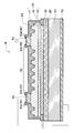
図3および図4に示すように、第1凸領域80に形成された第1凸部、および、第2凸領域90b(90)に形成された第2凸部は、先端が先細りした形状である。これにより、配光性が良好となっている。また、第1凸部および第2凸部は、先端が曲面で形成されている。したがって、先端が平坦な面で形成されている場合と比較して配光性が良い。また、図3および図4に示すように、第1凸部の高さは、第2凸部の高さの2倍以上である。さらに、第1凸部および第2凸部は、基端が隣り合う凸部の基端と隣接するように設けられている。つまり、凸部(第1凸部、第2凸部)は、隣の凸部との間に平坦な面を有していない。このように凸部が高密度に設けられているので光取り出し効率を高めることができる。したがって、配光性が良くなる。また、同じ深さであれば、凸部と隣の凸部との間に平坦な面を有しているものに比べて光出力が高くなる。 (First convex region and second convex region)
As shown in FIGS. 3 and 4, the first convex portion formed in the first
(第1製造方法)
図1に示した半導体発光素子の第1製造方法について、図5および図6を参照(適宜図1ないし図4参照)して説明する。図5および図6は、図1に示した半導体発光素子の製造工程を模式的に示す断面図である。 [Method for Manufacturing Semiconductor Light-Emitting Element]
(First manufacturing method)
A first method for manufacturing the semiconductor light emitting device shown in FIG. 1 will be described with reference to FIGS. 5 and 6 (refer to FIGS. 1 to 4 as appropriate). 5 and 6 are cross-sectional views schematically showing manufacturing steps of the semiconductor light emitting device shown in FIG.
図1に示した半導体発光素子の第2製造方法は、第1製造方法と同様に図5(a)~図5(e)および図6(a)~図6(b)にそれぞれ示す工程を行う。第2製造方法は、引き続いて行うn側電極50の形成方法に特徴がある。第2製造方法について、図7を参照(適宜図1ないし図6参照)して説明する。図7は、半導体発光素子の製造工程を模式的に示す断面図である。なお、図7では、半導体積層体40よりも下の層については図示を省略した。 (Second manufacturing method)
The second manufacturing method of the semiconductor light emitting device shown in FIG. 1 includes the steps shown in FIGS. 5 (a) to 5 (e) and FIGS. 6 (a) to 6 (b), respectively, as in the first manufacturing method. Do. The second manufacturing method is characterized by a subsequent method for forming the n-
本実施形態に係る半導体発光素子1の特性として、光出力、電極はがれ率、配光性について説明する。
(光出力)
本実施形態に係る半導体発光素子1は、光取り出し面に、比較的深い位置から比較的高い第1凸部を有する第1凸領域80と、比較的浅い位置から比較的低い第2凸部を有する第2凸領域90とを設けたので、第2凸部だけを全面に設けた発光素子よりも光出力を高めることができる。また、以下に示すように、電極はがれ率が低く、配光性が良いので、第1凸部を高く形成することができ、光出力を高めることができる。 [Characteristics of semiconductor light emitting device]
As the characteristics of the semiconductor light emitting device 1 according to this embodiment, the light output, the electrode peeling rate, and the light distribution will be described.
(Light output)
The semiconductor light emitting device 1 according to the present embodiment includes, on the light extraction surface, a first
比較として、第2凸部を第1凸部と同じように相対的に深い位置から高く設け、凹凸をドライエッチングにより形成したもの(以下、比較例1という)を、一例として、RIE(Reactive Ion Etching反応性イオンエッチング)で製造した。図12に示すように、比較例1を示す従来の半導体発光素子200は、主として、基板210と、メタライズ層220と、p側電極230と、半導体積層体240と、n側電極250と、保護膜260と、裏面メタライズ層270とからなる。半導体積層体240は、基板210に実装される側の面とは反対側の光取り出し面側から、n型半導体層241、発光層242およびp型半導体層243の順番に積層されて構成されている。また、n型半導体層241の表面には、電極非形成領域に凹凸280が規則的に形成されている。n側電極250は、n型半導体層241の表面である光取り出し面において、凹凸280以外の部分の上に設けられている。なお、図12では、凹凸280の一例を模式的に示しており、半導体発光素子200は、凹凸280において互いに隣り合う凹の間に平坦な面(上面)を有するか、または、互いに隣り合う凸の間に平坦な面(底面)の少なくとも一方を有する。 (Electrode peeling rate and light output)
As a comparison, a ridge (Reactive Ion) is used as an example in which the second protrusion is provided high from a relatively deep position like the first protrusion and the unevenness is formed by dry etching (hereinafter referred to as Comparative Example 1). Etching reactive ion etching). As shown in FIG. 12, the conventional semiconductor
図8は、本実施形態に係る半導体発光素子の指向性の一例を示す図である。ここで、ウェットエッチングのエッチング溶液として、KOH水溶液を用いて第1凸領域80および第2凸領域90を形成したもの(以下、実施例1という)を太い実線で示す。また、少なくとも第1凸部の高さが実施例1よりも小さくなるように加工量(深さ)を調整して形成したもの(以下、実施例2という)を細線で示す。さらに、比較として、前記した比較例1を破線で示し、前記した比較例2を一点鎖線で示す。 (Light distribution)
FIG. 8 is a diagram illustrating an example of directivity of the semiconductor light emitting device according to this embodiment. Here, a thick solid line represents the first
Claims (12)
- n型半導体層とp型半導体層との間に発光層を有する半導体積層体と、この半導体積層体が実装される基板と、前記半導体積層体が前記基板に実装される面とは反対側の光取り出し面の上に設けられた電極とを有し、前記光取り出し面に複数の凸部を備える半導体発光素子において、
前記複数の凸部は、第1凸領域と、第2凸領域とに設けられており、
前記第2凸領域は、前記第1凸領域と前記電極との間において前記電極と前記半導体積層体との界面と隣接した領域であり、
前記第1凸領域に設けられた第1凸部の基端は、前記界面よりも前記発光層側に位置し、
前記第2凸領域に設けられた第2凸部の基端は、前記第1凸部の基端よりも前記界面側に位置することを特徴とする半導体発光素子。 a semiconductor stacked body having a light emitting layer between an n-type semiconductor layer and a p-type semiconductor layer, a substrate on which the semiconductor stacked body is mounted, and a surface opposite to a surface on which the semiconductor stacked body is mounted on the substrate; In a semiconductor light emitting device having an electrode provided on the light extraction surface and having a plurality of convex portions on the light extraction surface,
The plurality of convex portions are provided in the first convex region and the second convex region,
The second convex region is a region adjacent to the interface between the electrode and the semiconductor stacked body between the first convex region and the electrode,
The base end of the first convex portion provided in the first convex region is located closer to the light emitting layer than the interface,
The base end of the 2nd convex part provided in the said 2nd convex area | region is located in the said interface side rather than the base end of the said 1st convex part, The semiconductor light-emitting device characterized by the above-mentioned. - 請求の範囲第1項に記載の半導体発光素子において、
前記第1凸部の基端から先端までの高さは、前記第2凸部の基端から先端までの高さよりも大きいことを特徴とする半導体発光素子。 In the semiconductor light emitting device according to claim 1,
The height from the base end of the 1st convex part to a front-end | tip is larger than the height from the base end of the said 2nd convex part to a front end, The semiconductor light-emitting device characterized by the above-mentioned. - 請求の範囲第1項または請求の範囲第2項に記載の半導体発光素子において、
前記第1凸部および前記第2凸部は、先端が先細りした形状であることを特徴とする半導体発光素子。 In the semiconductor light emitting device according to claim 1 or claim 2,
The first convex portion and the second convex portion have a shape with a tapered tip. - 請求の範囲第1項ないし請求の範囲第3項のいずれか一項に記載の半導体発光素子において、
少なくとも前記第2凸領域は前記電極を囲んで設けられていることを特徴とする半導体発光素子。 In the semiconductor light emitting device according to any one of claims 1 to 3,
At least the second convex region is provided so as to surround the electrode. - 請求の範囲第4項に記載の半導体発光素子において、
前記第1凸領域は前記第2凸領域および前記電極を囲んで設けられていることを特徴とする半導体発光素子。 In the semiconductor light-emitting device according to claim 4,
The semiconductor light emitting element, wherein the first convex region is provided so as to surround the second convex region and the electrode. - 請求の範囲第1項ないし請求の範囲第5項のいずれか一項に記載の半導体発光素子において、
前記光取り出し面には、前記電極が離間して設けられ、前記離間して設けられた電極に挟まれる領域に、前記第1凸領域および前記第2凸領域を有することを特徴とする半導体発光素子。 In the semiconductor light emitting device according to any one of claims 1 to 5,
A semiconductor light emitting device characterized in that the light extraction surface is provided with the electrodes spaced apart, and the first convex region and the second convex region are provided in a region sandwiched between the spaced electrodes. element. - 請求の範囲第1項ないし請求の範囲第6項のいずれか一項に記載の半導体発光素子において、
前記第1凸部および前記第2凸部は、先端が非平坦な形状に形成されていることを特徴とする半導体発光素子。 In the semiconductor light emitting device according to any one of claims 1 to 6,
The semiconductor light emitting device according to claim 1, wherein the first convex portion and the second convex portion are formed to have a non-flat tip. - 請求の範囲第1項ないし請求の範囲第7項のいずれか一項に記載の半導体発光素子において、
前記第1凸部および前記第2凸部は、基端が隣り合う凸部の基端と隣接するように設けられていることを特徴とする半導体発光素子。 In the semiconductor light emitting device according to any one of claims 1 to 7,
The first and second convex portions are provided so that their base ends are adjacent to the base ends of adjacent convex portions. - 請求の範囲第1項ないし請求の範囲第8項のいずれか一項に記載の半導体発光素子において、
前記第1凸領域において、前記第1凸部を、前記電極から離れるほど基端が前記発光層に近づくように形成したことを特徴とする半導体発光素子。 In the semiconductor light emitting device according to any one of claims 1 to 8,
In the first convex region, the first convex portion is formed so that the base end approaches the light emitting layer as the distance from the electrode increases. - 請求の範囲第1項ないし請求の範囲第9項のいずれか一項に記載の半導体発光素子において、
前記電極と前記半導体積層体との界面に、第3凸部をさらに有することを特徴とする半導体発光素子。 In the semiconductor light emitting device according to any one of claims 1 to 9,
A semiconductor light emitting element, further comprising a third convex portion at an interface between the electrode and the semiconductor laminate. - n型半導体層とp型半導体層との間に発光層を有する半導体積層体を形成する工程と、
前記半導体積層体の基板に実装される側とは反対側の光取り出し面を形成する一方の半導体層表面の電極形成予定領域を囲むように開口を有したレジストを、前記開口が前記レジストの積層方向に向かって閉塞するように形成する工程と、
前記レジストの上から前記半導体層表面にマスク材料を積層する工程と、
前記マスク材料が積層されたレジストを除去する工程と、
前記電極形成予定領域をマスクとして前記半導体層表面をエッチングする工程と、
を有することを特徴とする半導体発光素子の製造方法。 forming a semiconductor laminate having a light emitting layer between an n-type semiconductor layer and a p-type semiconductor layer;
A resist having an opening so as to surround an electrode formation scheduled region on one semiconductor layer surface forming a light extraction surface opposite to a side mounted on the substrate of the semiconductor laminate, and the opening is a laminate of the resist Forming so as to close in the direction;
Laminating a mask material on the semiconductor layer surface from above the resist;
Removing the resist layered with the mask material;
Etching the surface of the semiconductor layer using the electrode formation planned region as a mask;
A method for manufacturing a semiconductor light emitting device, comprising: - 請求の範囲第11項に記載の半導体発光素子の製造方法において、
前記マスク材料は、電極材料であることを特徴とする半導体発光素子の製造方法。 In the manufacturing method of the semiconductor light-emitting device according to claim 11,
The method of manufacturing a semiconductor light emitting device, wherein the mask material is an electrode material.
Priority Applications (7)
| Application Number | Priority Date | Filing Date | Title |
|---|---|---|---|
| KR1020107014047A KR101164663B1 (en) | 2007-12-28 | 2008-12-26 | Semiconductor light emitting element and method for manufacturing the same |
| EP08867680.4A EP2234182B1 (en) | 2007-12-28 | 2008-12-26 | Semiconductor light emitting element and method for manufacturing the same |
| US12/808,472 US8552445B2 (en) | 2007-12-28 | 2008-12-26 | Semiconductor light emitting device and method for manufacturing the same |
| CN2008801229171A CN101911317B (en) | 2007-12-28 | 2008-12-26 | Semiconductor light emitting element and method for manufacturing the same |
| JP2009548110A JP5310564B2 (en) | 2007-12-28 | 2008-12-26 | Semiconductor light emitting device and manufacturing method thereof |
| US14/021,551 US8883529B2 (en) | 2007-12-28 | 2013-09-09 | Method for manufacturing semiconductor light emitting device |
| US14/470,565 US9159868B2 (en) | 2007-12-28 | 2014-08-27 | Method for manufacturing semiconductor light emitting device |
Applications Claiming Priority (2)
| Application Number | Priority Date | Filing Date | Title |
|---|---|---|---|
| JP2007-341111 | 2007-12-28 | ||
| JP2007341111 | 2007-12-28 |
Related Child Applications (2)
| Application Number | Title | Priority Date | Filing Date |
|---|---|---|---|
| US12/808,472 A-371-Of-International US8552445B2 (en) | 2007-12-28 | 2008-12-26 | Semiconductor light emitting device and method for manufacturing the same |
| US14/021,551 Continuation US8883529B2 (en) | 2007-12-28 | 2013-09-09 | Method for manufacturing semiconductor light emitting device |
Publications (1)
| Publication Number | Publication Date |
|---|---|
| WO2009084670A1 true WO2009084670A1 (en) | 2009-07-09 |
Family
ID=40824383
Family Applications (1)
| Application Number | Title | Priority Date | Filing Date |
|---|---|---|---|
| PCT/JP2008/073821 WO2009084670A1 (en) | 2007-12-28 | 2008-12-26 | Semiconductor light emitting element and method for manufacturing the same |
Country Status (8)
| Country | Link |
|---|---|
| US (3) | US8552445B2 (en) |
| EP (1) | EP2234182B1 (en) |
| JP (2) | JP5310564B2 (en) |
| KR (1) | KR101164663B1 (en) |
| CN (1) | CN101911317B (en) |
| RU (1) | RU2436195C1 (en) |
| TW (1) | TW200945631A (en) |
| WO (1) | WO2009084670A1 (en) |
Cited By (17)
| Publication number | Priority date | Publication date | Assignee | Title |
|---|---|---|---|---|
| JP2011187873A (en) * | 2010-03-11 | 2011-09-22 | Toshiba Corp | Semiconductor light-emitting device |
| KR20120002822A (en) * | 2010-07-01 | 2012-01-09 | 삼성엘이디 주식회사 | Semiconductor light emitting diode and method of manufacturing thereof |
| JP2012033695A (en) * | 2010-07-30 | 2012-02-16 | Stanley Electric Co Ltd | Semiconductor light-emitting device |
| CN102694096A (en) * | 2011-03-21 | 2012-09-26 | 华新丽华股份有限公司 | Light emitting diode and method for manufacturing the same |
| JP2012533873A (en) * | 2009-07-17 | 2012-12-27 | オスラム オプト セミコンダクターズ ゲゼルシャフト ミット ベシュレンクテル ハフツング | Optoelectronic semiconductor component and method of manufacturing inorganic optoelectronic semiconductor component |
| JP2013106020A (en) * | 2011-11-17 | 2013-05-30 | Stanley Electric Co Ltd | Semiconductor light-emitting device and semiconductor light-emitting device manufacturing method |
| EP2423985A3 (en) * | 2010-08-26 | 2014-07-30 | Nichia Corporation | Semiconductor light emitting element |
| US8878214B2 (en) | 2010-12-28 | 2014-11-04 | Nichia Corporation | Semiconductor light emitting device |
| JP2015503849A (en) * | 2012-01-10 | 2015-02-02 | コーニンクレッカ フィリップス エヌ ヴェ | Controlled LED light output with selective area roughening |
| US20150048380A1 (en) * | 2012-04-02 | 2015-02-19 | Asahi Kasei E-Materials Corporation | Optical substrate, semiconductor light-emitting element and method of manufacturing semiconductor light-emitting element |
| JP2015076514A (en) * | 2013-10-09 | 2015-04-20 | エルシード株式会社 | Led element |
| US9093356B2 (en) | 2010-12-28 | 2015-07-28 | Nichia Corporation | Semiconductor light emitting element |
| WO2015156123A1 (en) * | 2014-04-07 | 2015-10-15 | 旭化成イーマテリアルズ株式会社 | Optical substrate and manufacturing method therefor, laminate, and resist removal liquid |
| JP2018022919A (en) * | 2017-10-06 | 2018-02-08 | エルシード株式会社 | LED element |
| JP2018050070A (en) * | 2017-11-21 | 2018-03-29 | ローム株式会社 | Semiconductor light emitting element |
| CN109075223A (en) * | 2016-04-27 | 2018-12-21 | 原子能和替代能源委员会 | The light emitting diode of at least one wider band gap middle layer at least one barrier layer including being located at luminous zone |
| JPWO2017154973A1 (en) * | 2016-03-08 | 2019-01-24 | アルパッド株式会社 | Semiconductor light emitting device and manufacturing method thereof |
Families Citing this family (27)
| Publication number | Priority date | Publication date | Assignee | Title |
|---|---|---|---|---|
| EP2234182B1 (en) * | 2007-12-28 | 2016-11-09 | Nichia Corporation | Semiconductor light emitting element and method for manufacturing the same |
| KR100999779B1 (en) | 2010-02-01 | 2010-12-08 | 엘지이노텍 주식회사 | Light emitting device, method for fabricating the same and light emitting device package |
| JP4996706B2 (en) * | 2010-03-03 | 2012-08-08 | 株式会社東芝 | Semiconductor light emitting device and manufacturing method thereof |
| KR101081135B1 (en) | 2010-03-15 | 2011-11-07 | 엘지이노텍 주식회사 | Light emitting device, method for fabricating the light emitting device and light emitting device package |
| KR101673955B1 (en) * | 2010-07-02 | 2016-11-08 | 삼성전자주식회사 | Semiconductor Light Emitting Device and Manufacturing Method of The Same |
| KR20120092325A (en) * | 2011-02-11 | 2012-08-21 | 서울옵토디바이스주식회사 | Light emitting diode having photonic crystal structure and method of fabricating the same |
| JP5603813B2 (en) * | 2011-03-15 | 2014-10-08 | 株式会社東芝 | Semiconductor light emitting device and light emitting device |
| CN104040735B (en) | 2011-10-06 | 2017-08-25 | 皇家飞利浦有限公司 | The surface treatment of light emitting semiconductor device |
| KR101827975B1 (en) | 2011-10-10 | 2018-03-29 | 엘지이노텍 주식회사 | Light emitting device |
| US9847372B2 (en) * | 2011-12-01 | 2017-12-19 | Micron Technology, Inc. | Solid state transducer devices with separately controlled regions, and associated systems and methods |
| KR101894025B1 (en) | 2011-12-16 | 2018-09-03 | 엘지이노텍 주식회사 | Light emitting device |
| JP5292456B2 (en) | 2011-12-28 | 2013-09-18 | Dowaエレクトロニクス株式会社 | Group III nitride semiconductor device and manufacturing method thereof |
| US9263255B2 (en) * | 2012-03-19 | 2016-02-16 | Seoul Viosys Co., Ltd. | Method for separating epitaxial layers from growth substrates, and semiconductor device using same |
| KR102099441B1 (en) * | 2013-12-19 | 2020-04-09 | 엘지이노텍 주식회사 | Light emittng device |
| JP6106120B2 (en) * | 2014-03-27 | 2017-03-29 | 株式会社東芝 | Semiconductor light emitting device |
| CN105023983A (en) * | 2014-04-24 | 2015-11-04 | 展晶科技(深圳)有限公司 | Flip-chip type semiconductor light-emitting element and manufacturing method thereof |
| JP2016146389A (en) * | 2015-02-06 | 2016-08-12 | 株式会社東芝 | Semiconductor light-emitting element and method of manufacturing the same |
| JP2016171277A (en) * | 2015-03-16 | 2016-09-23 | 株式会社東芝 | Semiconductor light-emitting element and manufacturing method thereof |
| JP6582738B2 (en) * | 2015-08-26 | 2019-10-02 | 日亜化学工業株式会社 | Light emitting element and light emitting device |
| JP6738169B2 (en) * | 2016-03-11 | 2020-08-12 | Dowaエレクトロニクス株式会社 | Semiconductor optical device and manufacturing method thereof |
| CN106784185B (en) * | 2016-12-22 | 2019-05-14 | 天津三安光电有限公司 | Light emitting diode and preparation method thereof |
| KR102565148B1 (en) | 2018-06-27 | 2023-08-18 | 서울바이오시스 주식회사 | Flip chip type light emitting diode chip and light emitting device including the same |
| US11271136B2 (en) * | 2018-11-07 | 2022-03-08 | Seoul Viosys Co., Ltd | Light emitting device |
| RU2713908C2 (en) * | 2018-11-23 | 2020-02-11 | Общество С Ограниченной Ответственностью "Кубик Мкм" (Ооо "Кубик-Мкм") | Microcontact for surface mounting and array of microcontacts |
| DE102019106546A1 (en) * | 2019-03-14 | 2020-09-17 | OSRAM Opto Semiconductors Gesellschaft mit beschränkter Haftung | METHOD FOR MANUFACTURING OPTOELECTRONIC SEMICONDUCTOR COMPONENTS AND OPTOELECTRONIC SEMICONDUCTOR COMPONENTS |
| DE102020112414A1 (en) | 2020-05-07 | 2021-11-11 | OSRAM Opto Semiconductors Gesellschaft mit beschränkter Haftung | Radiation-emitting semiconductor component and method for producing a radiation-emitting semiconductor component |
| CN112133804B (en) * | 2020-08-04 | 2022-03-18 | 华灿光电(苏州)有限公司 | Light emitting diode chip and manufacturing method thereof |
Citations (12)
| Publication number | Priority date | Publication date | Assignee | Title |
|---|---|---|---|---|
| JPH10200162A (en) * | 1997-01-10 | 1998-07-31 | Sanken Electric Co Ltd | Semiconductor light emitting element |
| JPH1154769A (en) * | 1997-07-30 | 1999-02-26 | Toshiba Corp | Optical packaging component and its manufacture |
| JP2000196152A (en) | 1998-12-24 | 2000-07-14 | Toshiba Corp | Semiconductor light emitting device and manufacture thereof |
| JP2003069075A (en) | 2001-08-28 | 2003-03-07 | Nichia Chem Ind Ltd | Gallium nitride compound semiconductor device |
| JP2004119839A (en) * | 2002-09-27 | 2004-04-15 | Toshiba Corp | Optical semiconductor device and its manufacturing method |
| JP2004356279A (en) * | 2003-05-28 | 2004-12-16 | Hitachi Cable Ltd | Method for manufacturing semiconductor light emitting element |
| JP2005005679A (en) | 2003-04-15 | 2005-01-06 | Matsushita Electric Ind Co Ltd | Semiconductor light emitting device and its manufacturing method |
| JP2005244201A (en) | 2004-01-28 | 2005-09-08 | Matsushita Electric Ind Co Ltd | Semiconductor luminous element and manufacturing method of the same |
| JP2006147787A (en) | 2004-11-18 | 2006-06-08 | Sony Corp | Light emitting element and its manufacturing method |
| JP2007067209A (en) | 2005-08-31 | 2007-03-15 | Sanyo Electric Co Ltd | Nitride-based semiconductor light emitting element and method of manufacturing same |
| JP2007088277A (en) | 2005-09-22 | 2007-04-05 | Matsushita Electric Works Ltd | Semiconductor light-emitting element and manufacturing method thereof |
| JP2008066554A (en) * | 2006-09-08 | 2008-03-21 | Sanken Electric Co Ltd | Semiconductor light emitting device |
Family Cites Families (25)
| Publication number | Priority date | Publication date | Assignee | Title |
|---|---|---|---|---|
| JPS5840872A (en) * | 1981-09-03 | 1983-03-09 | Nec Corp | Semiconductor light-emitting device |
| JPS6254485A (en) * | 1985-09-03 | 1987-03-10 | Toshiba Corp | Preparation for semiconductor light emitting element |
| JPH06334218A (en) * | 1993-05-24 | 1994-12-02 | Matsushita Electric Ind Co Ltd | Led element |
| JPH0738146A (en) * | 1993-07-20 | 1995-02-07 | Victor Co Of Japan Ltd | Semiconductor light emitting device |
| US5779924A (en) * | 1996-03-22 | 1998-07-14 | Hewlett-Packard Company | Ordered interface texturing for a light emitting device |
| TW444417B (en) * | 2000-02-14 | 2001-07-01 | Rohm Co Ltd | Method for making a semiconductor light emitting element |
| JP2003188410A (en) | 2001-12-19 | 2003-07-04 | Daido Steel Co Ltd | Light emitting diode chip |
| JP3802424B2 (en) * | 2002-01-15 | 2006-07-26 | 株式会社東芝 | Semiconductor light emitting device and manufacturing method thereof |
| JP3782357B2 (en) * | 2002-01-18 | 2006-06-07 | 株式会社東芝 | Manufacturing method of semiconductor light emitting device |
| TW200509408A (en) * | 2003-08-20 | 2005-03-01 | Epistar Corp | Nitride light-emitting device with high light-emitting efficiency |
| JP2005116615A (en) * | 2003-10-03 | 2005-04-28 | Dowa Mining Co Ltd | Semiconductor light emitting element and its manufacturing method |
| CN100459189C (en) * | 2003-11-19 | 2009-02-04 | 日亚化学工业株式会社 | Semiconductor element and manufacturing method for the same |
| DE10355581B4 (en) * | 2003-11-28 | 2010-01-14 | Advanced Micro Devices, Inc., Sunnyvale | Method and technology for producing a gate electrode using a hard mask |
| CN100356593C (en) * | 2004-03-30 | 2007-12-19 | 晶元光电股份有限公司 | High efficient nitride series light-emitting element |
| US7534633B2 (en) * | 2004-07-02 | 2009-05-19 | Cree, Inc. | LED with substrate modifications for enhanced light extraction and method of making same |
| US7476910B2 (en) * | 2004-09-10 | 2009-01-13 | Kabushiki Kaisha Toshiba | Semiconductor light emitting device and method for manufacturing the same |
| US7897420B2 (en) * | 2005-01-11 | 2011-03-01 | SemiLEDs Optoelectronics Co., Ltd. | Light emitting diodes (LEDs) with improved light extraction by roughening |
| KR100631969B1 (en) * | 2005-02-28 | 2006-10-11 | 삼성전기주식회사 | Nitride semiconductor light emitting device |
| JP4297084B2 (en) * | 2005-06-13 | 2009-07-15 | 住友電気工業株式会社 | LIGHT EMITTING DEVICE MANUFACTURING METHOD AND LIGHT EMITTING DEVICE |
| JP2007165409A (en) * | 2005-12-09 | 2007-06-28 | Rohm Co Ltd | Semiconductor light emitting element and method of manufacturing same |
| KR100649767B1 (en) | 2005-12-26 | 2006-11-27 | 삼성전기주식회사 | Vertical nitride semiconductor light emitting device |
| JP2007220865A (en) * | 2006-02-16 | 2007-08-30 | Sumitomo Chemical Co Ltd | Group iii nitride semiconductor light emitting device, and its manufacturing method |
| CN100555689C (en) * | 2006-06-15 | 2009-10-28 | 夏普株式会社 | Nitride semiconductor luminescent element and manufacture method thereof |
| US7692203B2 (en) * | 2006-10-20 | 2010-04-06 | Hitachi Cable, Ltd. | Semiconductor light emitting device |
| EP2234182B1 (en) * | 2007-12-28 | 2016-11-09 | Nichia Corporation | Semiconductor light emitting element and method for manufacturing the same |
-
2008
- 2008-12-26 EP EP08867680.4A patent/EP2234182B1/en active Active
- 2008-12-26 JP JP2009548110A patent/JP5310564B2/en active Active
- 2008-12-26 TW TW097151166A patent/TW200945631A/en unknown
- 2008-12-26 KR KR1020107014047A patent/KR101164663B1/en active IP Right Grant
- 2008-12-26 CN CN2008801229171A patent/CN101911317B/en active Active
- 2008-12-26 WO PCT/JP2008/073821 patent/WO2009084670A1/en active Application Filing
- 2008-12-26 RU RU2010131486/28A patent/RU2436195C1/en active
- 2008-12-26 US US12/808,472 patent/US8552445B2/en active Active
-
2013
- 2013-07-03 JP JP2013139370A patent/JP5545398B2/en active Active
- 2013-09-09 US US14/021,551 patent/US8883529B2/en active Active
-
2014
- 2014-08-27 US US14/470,565 patent/US9159868B2/en active Active
Patent Citations (12)
| Publication number | Priority date | Publication date | Assignee | Title |
|---|---|---|---|---|
| JPH10200162A (en) * | 1997-01-10 | 1998-07-31 | Sanken Electric Co Ltd | Semiconductor light emitting element |
| JPH1154769A (en) * | 1997-07-30 | 1999-02-26 | Toshiba Corp | Optical packaging component and its manufacture |
| JP2000196152A (en) | 1998-12-24 | 2000-07-14 | Toshiba Corp | Semiconductor light emitting device and manufacture thereof |
| JP2003069075A (en) | 2001-08-28 | 2003-03-07 | Nichia Chem Ind Ltd | Gallium nitride compound semiconductor device |
| JP2004119839A (en) * | 2002-09-27 | 2004-04-15 | Toshiba Corp | Optical semiconductor device and its manufacturing method |
| JP2005005679A (en) | 2003-04-15 | 2005-01-06 | Matsushita Electric Ind Co Ltd | Semiconductor light emitting device and its manufacturing method |
| JP2004356279A (en) * | 2003-05-28 | 2004-12-16 | Hitachi Cable Ltd | Method for manufacturing semiconductor light emitting element |
| JP2005244201A (en) | 2004-01-28 | 2005-09-08 | Matsushita Electric Ind Co Ltd | Semiconductor luminous element and manufacturing method of the same |
| JP2006147787A (en) | 2004-11-18 | 2006-06-08 | Sony Corp | Light emitting element and its manufacturing method |
| JP2007067209A (en) | 2005-08-31 | 2007-03-15 | Sanyo Electric Co Ltd | Nitride-based semiconductor light emitting element and method of manufacturing same |
| JP2007088277A (en) | 2005-09-22 | 2007-04-05 | Matsushita Electric Works Ltd | Semiconductor light-emitting element and manufacturing method thereof |
| JP2008066554A (en) * | 2006-09-08 | 2008-03-21 | Sanken Electric Co Ltd | Semiconductor light emitting device |
Non-Patent Citations (1)
| Title |
|---|
| See also references of EP2234182A4 |
Cited By (26)
| Publication number | Priority date | Publication date | Assignee | Title |
|---|---|---|---|---|
| EP2454763B1 (en) * | 2009-07-17 | 2017-01-18 | OSRAM Opto Semiconductors GmbH | Optoelectronic semiconductor component and method for producing an inorganic optoelectronic semiconductor component |
| JP2012533873A (en) * | 2009-07-17 | 2012-12-27 | オスラム オプト セミコンダクターズ ゲゼルシャフト ミット ベシュレンクテル ハフツング | Optoelectronic semiconductor component and method of manufacturing inorganic optoelectronic semiconductor component |
| US8698178B2 (en) | 2009-07-17 | 2014-04-15 | Osram Opto Semiconductors Gmbh | Optoelectronic semiconductor component and method for producing an inorganic optoelectronic semiconductor component |
| KR101614106B1 (en) * | 2009-07-17 | 2016-04-20 | 오스람 옵토 세미컨덕터스 게엠베하 | Optoelectronic semiconductor component and method for producing an inorganic optoelectronic semiconductor component |
| JP2011187873A (en) * | 2010-03-11 | 2011-09-22 | Toshiba Corp | Semiconductor light-emitting device |
| US8729583B2 (en) | 2010-03-11 | 2014-05-20 | Kabushiki Kaisha Toshiba | Semiconductor light-emitting device |
| KR20120002822A (en) * | 2010-07-01 | 2012-01-09 | 삼성엘이디 주식회사 | Semiconductor light emitting diode and method of manufacturing thereof |
| EP2403022A3 (en) * | 2010-07-01 | 2015-03-11 | Samsung Electronics Co., Ltd. | Semiconductor light emitting diode and manufacturing method thereof |
| KR101671793B1 (en) * | 2010-07-01 | 2016-11-04 | 삼성전자주식회사 | Semiconductor Light Emitting Diode and Method of manufacturing thereof |
| JP2012033695A (en) * | 2010-07-30 | 2012-02-16 | Stanley Electric Co Ltd | Semiconductor light-emitting device |
| EP2423985A3 (en) * | 2010-08-26 | 2014-07-30 | Nichia Corporation | Semiconductor light emitting element |
| US8878214B2 (en) | 2010-12-28 | 2014-11-04 | Nichia Corporation | Semiconductor light emitting device |
| US9093356B2 (en) | 2010-12-28 | 2015-07-28 | Nichia Corporation | Semiconductor light emitting element |
| CN102694096A (en) * | 2011-03-21 | 2012-09-26 | 华新丽华股份有限公司 | Light emitting diode and method for manufacturing the same |
| JP2013106020A (en) * | 2011-11-17 | 2013-05-30 | Stanley Electric Co Ltd | Semiconductor light-emitting device and semiconductor light-emitting device manufacturing method |
| JP2015503849A (en) * | 2012-01-10 | 2015-02-02 | コーニンクレッカ フィリップス エヌ ヴェ | Controlled LED light output with selective area roughening |
| US20150048380A1 (en) * | 2012-04-02 | 2015-02-19 | Asahi Kasei E-Materials Corporation | Optical substrate, semiconductor light-emitting element and method of manufacturing semiconductor light-emitting element |
| US9614136B2 (en) * | 2012-04-02 | 2017-04-04 | Asahi Kasei Kabushiki Kaisha | Optical substrate, semiconductor light-emitting element and method of manufacturing semiconductor light-emitting element |
| JP2015076514A (en) * | 2013-10-09 | 2015-04-20 | エルシード株式会社 | Led element |
| WO2015156123A1 (en) * | 2014-04-07 | 2015-10-15 | 旭化成イーマテリアルズ株式会社 | Optical substrate and manufacturing method therefor, laminate, and resist removal liquid |
| JPWO2015156123A1 (en) * | 2014-04-07 | 2017-04-13 | 旭化成株式会社 | OPTICAL SUBSTRATE, ITS MANUFACTURING METHOD, LAMINATE, RESIST REMOVAL |
| US11145790B2 (en) | 2016-03-08 | 2021-10-12 | Alpad Corporation | Semiconductor light emitting device and method for manufacturing same |
| JPWO2017154973A1 (en) * | 2016-03-08 | 2019-01-24 | アルパッド株式会社 | Semiconductor light emitting device and manufacturing method thereof |
| CN109075223A (en) * | 2016-04-27 | 2018-12-21 | 原子能和替代能源委员会 | The light emitting diode of at least one wider band gap middle layer at least one barrier layer including being located at luminous zone |
| JP2018022919A (en) * | 2017-10-06 | 2018-02-08 | エルシード株式会社 | LED element |
| JP2018050070A (en) * | 2017-11-21 | 2018-03-29 | ローム株式会社 | Semiconductor light emitting element |
Also Published As
| Publication number | Publication date |
|---|---|
| JP2013211595A (en) | 2013-10-10 |
| CN101911317B (en) | 2012-06-06 |
| TW200945631A (en) | 2009-11-01 |
| US20100264443A1 (en) | 2010-10-21 |
| CN101911317A (en) | 2010-12-08 |
| US8552445B2 (en) | 2013-10-08 |
| KR101164663B1 (en) | 2012-07-12 |
| JPWO2009084670A1 (en) | 2011-05-19 |
| US20140370630A1 (en) | 2014-12-18 |
| KR20100085193A (en) | 2010-07-28 |
| US9159868B2 (en) | 2015-10-13 |
| US8883529B2 (en) | 2014-11-11 |
| EP2234182A4 (en) | 2014-09-03 |
| JP5310564B2 (en) | 2013-10-09 |
| EP2234182B1 (en) | 2016-11-09 |
| RU2436195C1 (en) | 2011-12-10 |
| JP5545398B2 (en) | 2014-07-09 |
| US20140038328A1 (en) | 2014-02-06 |
| TWI377705B (en) | 2012-11-21 |
| EP2234182A1 (en) | 2010-09-29 |
Similar Documents
| Publication | Publication Date | Title |
|---|---|---|
| JP5545398B2 (en) | Manufacturing method of semiconductor light emitting device | |
| JP5493252B2 (en) | Semiconductor light emitting device | |
| JP5282503B2 (en) | Semiconductor light emitting device | |
| EP2190036B1 (en) | Light emitting device and method for manufacturing the same | |
| CN101355128B (en) | Semiconductor light-emitting element and semiconductor light-emitting element manufacturing method | |
| TWI545801B (en) | Semiconductor light emitting element and method of manufacturing the semiconductor light emitting element | |
| WO2012091008A1 (en) | Semiconductor light-emitting device | |
| CN106252490B (en) | Semiconductor light-emitting apparatus | |
| JP6040769B2 (en) | Light emitting device and manufacturing method thereof | |
| TWI431815B (en) | Semiconductor light emitting device | |
| TWI568024B (en) | Nitride semiconductor light emitting device and manufacturing method thereof | |
| US8013353B2 (en) | Light-emitting element | |
| JP5045001B2 (en) | Semiconductor light emitting device | |
| WO2005027232A1 (en) | GaN LIGHT-EMITTING DIODE | |
| JP6119906B2 (en) | Light emitting element | |
| EP2228837B1 (en) | Light emitting device, fabrication method thereof, and light emitting apparatus | |
| WO2012091007A1 (en) | Semiconductor light-emitting element | |
| CN113964245A (en) | Light-emitting element and method for manufacturing light-emitting element | |
| CN106887489A (en) | Semiconductor light-emitting elements | |
| JP2011009648A (en) | Light-emitting element |
Legal Events
| Date | Code | Title | Description |
|---|---|---|---|
| WWE | Wipo information: entry into national phase |
Ref document number: 200880122917.1 Country of ref document: CN |
|
| ENP | Entry into the national phase |
Ref document number: 2009548110 Country of ref document: JP Kind code of ref document: A |
|
| 121 | Ep: the epo has been informed by wipo that ep was designated in this application |
Ref document number: 08867680 Country of ref document: EP Kind code of ref document: A1 |
|
| WWE | Wipo information: entry into national phase |
Ref document number: 12808472 Country of ref document: US |
|
| ENP | Entry into the national phase |
Ref document number: 20107014047 Country of ref document: KR Kind code of ref document: A |
|
| NENP | Non-entry into the national phase |
Ref country code: DE |
|
| WWE | Wipo information: entry into national phase |
Ref document number: 5023/DELNP/2010 Country of ref document: IN |
|
| REEP | Request for entry into the european phase |
Ref document number: 2008867680 Country of ref document: EP |
|
| WWE | Wipo information: entry into national phase |
Ref document number: 2008867680 Country of ref document: EP |
|
| WWE | Wipo information: entry into national phase |
Ref document number: 2010131486 Country of ref document: RU |