EP2454763B1 - Optoelectronic semiconductor component and method for producing an inorganic optoelectronic semiconductor component - Google Patents
Optoelectronic semiconductor component and method for producing an inorganic optoelectronic semiconductor component Download PDFInfo
- Publication number
- EP2454763B1 EP2454763B1 EP10724846.0A EP10724846A EP2454763B1 EP 2454763 B1 EP2454763 B1 EP 2454763B1 EP 10724846 A EP10724846 A EP 10724846A EP 2454763 B1 EP2454763 B1 EP 2454763B1
- Authority
- EP
- European Patent Office
- Prior art keywords
- layer
- encapsulation layer
- metal mirror
- mirror
- carrier
- Prior art date
- Legal status (The legal status is an assumption and is not a legal conclusion. Google has not performed a legal analysis and makes no representation as to the accuracy of the status listed.)
- Not-in-force
Links
Images

Classifications
-
- H—ELECTRICITY
- H01—ELECTRIC ELEMENTS
- H01L—SEMICONDUCTOR DEVICES NOT COVERED BY CLASS H10
- H01L33/00—Semiconductor devices with at least one potential-jump barrier or surface barrier specially adapted for light emission; Processes or apparatus specially adapted for the manufacture or treatment thereof or of parts thereof; Details thereof
- H01L33/44—Semiconductor devices with at least one potential-jump barrier or surface barrier specially adapted for light emission; Processes or apparatus specially adapted for the manufacture or treatment thereof or of parts thereof; Details thereof characterised by the coatings, e.g. passivation layer or anti-reflective coating
-
- H—ELECTRICITY
- H01—ELECTRIC ELEMENTS
- H01L—SEMICONDUCTOR DEVICES NOT COVERED BY CLASS H10
- H01L24/00—Arrangements for connecting or disconnecting semiconductor or solid-state bodies; Methods or apparatus related thereto
- H01L24/01—Means for bonding being attached to, or being formed on, the surface to be connected, e.g. chip-to-package, die-attach, "first-level" interconnects; Manufacturing methods related thereto
- H01L24/02—Bonding areas ; Manufacturing methods related thereto
- H01L24/04—Structure, shape, material or disposition of the bonding areas prior to the connecting process
- H01L24/05—Structure, shape, material or disposition of the bonding areas prior to the connecting process of an individual bonding area
-
- H—ELECTRICITY
- H01—ELECTRIC ELEMENTS
- H01L—SEMICONDUCTOR DEVICES NOT COVERED BY CLASS H10
- H01L2224/00—Indexing scheme for arrangements for connecting or disconnecting semiconductor or solid-state bodies and methods related thereto as covered by H01L24/00
- H01L2224/01—Means for bonding being attached to, or being formed on, the surface to be connected, e.g. chip-to-package, die-attach, "first-level" interconnects; Manufacturing methods related thereto
- H01L2224/02—Bonding areas; Manufacturing methods related thereto
- H01L2224/04—Structure, shape, material or disposition of the bonding areas prior to the connecting process
- H01L2224/04042—Bonding areas specifically adapted for wire connectors, e.g. wirebond pads
-
- H—ELECTRICITY
- H01—ELECTRIC ELEMENTS
- H01L—SEMICONDUCTOR DEVICES NOT COVERED BY CLASS H10
- H01L2224/00—Indexing scheme for arrangements for connecting or disconnecting semiconductor or solid-state bodies and methods related thereto as covered by H01L24/00
- H01L2224/01—Means for bonding being attached to, or being formed on, the surface to be connected, e.g. chip-to-package, die-attach, "first-level" interconnects; Manufacturing methods related thereto
- H01L2224/02—Bonding areas; Manufacturing methods related thereto
- H01L2224/04—Structure, shape, material or disposition of the bonding areas prior to the connecting process
- H01L2224/05—Structure, shape, material or disposition of the bonding areas prior to the connecting process of an individual bonding area
- H01L2224/0554—External layer
- H01L2224/0555—Shape
- H01L2224/05556—Shape in side view
-
- H—ELECTRICITY
- H01—ELECTRIC ELEMENTS
- H01L—SEMICONDUCTOR DEVICES NOT COVERED BY CLASS H10
- H01L2224/00—Indexing scheme for arrangements for connecting or disconnecting semiconductor or solid-state bodies and methods related thereto as covered by H01L24/00
- H01L2224/01—Means for bonding being attached to, or being formed on, the surface to be connected, e.g. chip-to-package, die-attach, "first-level" interconnects; Manufacturing methods related thereto
- H01L2224/42—Wire connectors; Manufacturing methods related thereto
- H01L2224/47—Structure, shape, material or disposition of the wire connectors after the connecting process
- H01L2224/48—Structure, shape, material or disposition of the wire connectors after the connecting process of an individual wire connector
- H01L2224/4805—Shape
- H01L2224/4809—Loop shape
- H01L2224/48091—Arched
-
- H—ELECTRICITY
- H01—ELECTRIC ELEMENTS
- H01L—SEMICONDUCTOR DEVICES NOT COVERED BY CLASS H10
- H01L2924/00—Indexing scheme for arrangements or methods for connecting or disconnecting semiconductor or solid-state bodies as covered by H01L24/00
- H01L2924/10—Details of semiconductor or other solid state devices to be connected
- H01L2924/11—Device type
- H01L2924/12—Passive devices, e.g. 2 terminal devices
- H01L2924/1204—Optical Diode
- H01L2924/12041—LED
-
- H—ELECTRICITY
- H01—ELECTRIC ELEMENTS
- H01L—SEMICONDUCTOR DEVICES NOT COVERED BY CLASS H10
- H01L2924/00—Indexing scheme for arrangements or methods for connecting or disconnecting semiconductor or solid-state bodies as covered by H01L24/00
- H01L2924/10—Details of semiconductor or other solid state devices to be connected
- H01L2924/11—Device type
- H01L2924/12—Passive devices, e.g. 2 terminal devices
- H01L2924/1204—Optical Diode
- H01L2924/12043—Photo diode
-
- H—ELECTRICITY
- H01—ELECTRIC ELEMENTS
- H01L—SEMICONDUCTOR DEVICES NOT COVERED BY CLASS H10
- H01L2933/00—Details relating to devices covered by the group H01L33/00 but not provided for in its subgroups
- H01L2933/0008—Processes
- H01L2933/0025—Processes relating to coatings
-
- H—ELECTRICITY
- H01—ELECTRIC ELEMENTS
- H01L—SEMICONDUCTOR DEVICES NOT COVERED BY CLASS H10
- H01L33/00—Semiconductor devices with at least one potential-jump barrier or surface barrier specially adapted for light emission; Processes or apparatus specially adapted for the manufacture or treatment thereof or of parts thereof; Details thereof
- H01L33/36—Semiconductor devices with at least one potential-jump barrier or surface barrier specially adapted for light emission; Processes or apparatus specially adapted for the manufacture or treatment thereof or of parts thereof; Details thereof characterised by the electrodes
- H01L33/40—Materials therefor
- H01L33/405—Reflective materials
Definitions
- An optoelectronic semiconductor component is specified.
- a method for producing an inorganic optoelectronic semiconductor device is specified.
- the publication WO 2009/045082 A2 relates to a light emitting diode and a manufacturing method thereof.
- the publication US 2008/0113462 A1 relates to a manufacturing method for a vertically emitting, radiation-generating semiconductor device.
- An object to be solved is to specify an optoelectronic semiconductor component with a high light extraction efficiency. Another object to be solved is to specify a method for producing such an optoelectronic semiconductor component.
- the optoelectronic semiconductor component includes at least one semiconductor layer sequence.
- the preferably inorganic semiconductor layer sequence may be a light-emitting diode, a laser diode or a photodiode.
- the semiconductor layer sequence is preferably a thin-film layer sequence, as for example in the document DE 10 2007 004 304 A1 specified.
- the semiconductor layer sequence includes one or more active layers. Active means that the corresponding layer is adapted to emit or absorb electromagnetic radiation.
- the optoelectronic semiconductor component comprises a carrier.
- the carrier is preferably configured to carry and mechanically support the semiconductor layer sequence.
- the carrier is in particular a rigid, bending-resistant solid material in the context of the loads occurring in the operation according to the invention of the semiconductor component.
- the support comprises or consists of a semiconductor material such as germanium or silicon, of a metal such as Cu, Ni, Ag or Mo or of an electrically insulating material such as Al 2 O 3 , AlN or SiN x .
- the carrier may be different from a growth substrate of the semiconductor layer sequence.
- the semiconductor layer sequence is attached to the carrier. This may mean that there are one or more layers between the semiconductor layer sequence and the carrier, via which adhesion promotion and a firm connection between the semiconductor layer sequence and the carrier is ensured. In particular, there is no direct contact between a material of the carrier and the semiconductor layer sequence.
- the optoelectronic semiconductor component comprises a metal mirror.
- the metal mirror is located between the carrier and the semiconductor layer sequence.
- the entire metal mirror is arranged so that it is completely between the semiconductor layer sequence and the carrier.
- the metal mirror is configured to reflect a radiation to be emitted or received by the active layer.
- Metal mirror means that the mirror consists mainly or completely of a metal or a metal alloy.
- the metal mirror is a silver mirror.
- An electrical connection between the carrier and the semiconductor layer sequence can take place via the preferably electrically conductive metal mirror.
- the metal mirror may be in direct contact with the semiconductor layer sequence.
- the metal mirror comprises or consists of a material, such as silver, which is chemically damaged under the influence of oxygen or water.
- a material of the metal mirror for example, too Silver, tend to migrate, especially under the influence of moisture and / or electrical voltage.
- the carrier and the semiconductor layer sequence project beyond the metal mirror in a lateral direction.
- the lateral direction is, for example, a direction extending in parallel along a main extension direction of the carrier.
- the metal mirror in each lateral direction is surmounted by both the carrier and the semiconductor layer sequence.
- both the carrier and the semiconductor layer sequence in the lateral direction are preferably over the metal mirror all around or on all sides.
- the metal mirror in the lateral direction is surrounded directly by a permeable and electrically insulating or electrically conductive encapsulation layer for a radiation to be emitted or received by the semiconductor layer sequence.
- a material of the encapsulation layer in particular all around, directly adjoins a material of the metal mirror, for example all boundary surfaces of the metal mirror, which do not face the carrier or the semiconductor layer sequence.
- the optoelectronic semiconductor component includes a carrier and at least one semiconductor layer sequence.
- the semiconductor layer sequence has at least one active layer.
- the semiconductor layer sequence is further attached to the carrier.
- the semiconductor device includes a metal mirror, which is located between the carrier and the semiconductor layer sequence.
- the carrier and the semiconductor layer sequence project beyond the metal mirror in the lateral direction.
- the metal mirror is in Lateral direction directly surrounded by a radiation-transmissive and electrically insulating or electrically conductive encapsulation layer.
- the metal mirror Due to the fact that the metal mirror is in particular completely surrounded by the encapsulation layer in the lateral direction, so that no boundary surface of the metal mirror or the boundary surface of the metal mirror facing the support is exposed, the metal mirror can be protected against damage, for example by oxidation. Also, migration of components of the metal mirror, for example on lateral boundary surfaces of the semiconductor layer sequence, can be prevented or greatly reduced by the encapsulation layer.
- a radiation-permeable encapsulation layer a coupling-out efficiency of a radiation generated in the semiconductor component, for example, is substantially absorbed, since substantially no radiation is absorbed by the encapsulation layer and, in particular, efficient reflection and deflection of the radiation can take place by further layers underlying the encapsulation layer.
- the optoelectronic semiconductor component comprises a material of the encapsulation layer to a specific diffusion constant for water and / or oxygen of at most 10 -5 g / (m 2 d).
- the specific diffusion constant is in this case calculated in particular to a material thickness of 0.1 ⁇ m.
- the diffusion constant is preferably at most 5 ⁇ 10 -6 g / (m 2 d), in particular at most 10 -6 g / (m 2 d).
- the encapsulation layer or the encapsulation layer comprises a silicon oxide, an aluminum oxide and / or a zirconium oxide.
- the encapsulation layer may comprise or consist of one of the following materials: TiO 2 , HfO 2 , SnO 2 , SiC, Zr (SiO 4 ), Pb 3 (Si 2 O 7 ), Na (AlSiO 4 ), Si 3 N 4 , AlN, GaN.
- Other transparent, moisture-stable oxides, carbides and / or nitrides can be used for the encapsulation layer.
- the metal mirror has a thickness of between 100 nm and 200 nm, in particular between 100 nm and 150 nm inclusive.
- a thickness of the encapsulation layer is between 20 nm and 100 nm inclusive, in particular between 35 nm and 70 nm inclusive. In this case, the thickness of the encapsulation layer is to be measured in particular in a direction parallel to a growth direction of the encapsulation layer. If the encapsulation layer has a plurality of coalesced subareas, the thickness must be determined in each case for the individual subregions, for example, up to a seam at which the individual subareas adjoin one another.
- the optoelectronic semiconductor device comprises a second mirror layer which extends between the metal mirror and the Carrier is located.
- the second mirror layer preferably directly adjoins the metal mirror so that a material of the second mirror layer is in physical contact with a material of the metal mirror.
- the second mirror layer is electrically conductive and, for example, also formed from at least one metal.
- a material of the second mirror layer is, for example, Cr or a Cr alloy.
- Further possible materials for the second mirror layer are Ti, Ti 3 N 4 , TiW, TiW (N), Au, Pt, Pd and / or Ni.
- the material of the second mirror layer does not tend, or at least less strongly, than the material of the encapsulation layer to migration and corrosion under the influence of moisture and / or oxygen.
- the second mirror layer likewise preferably projects beyond the encapsulation layer in the lateral direction, in particular all the way around.
- the second mirror layer is configured to reflect an electromagnetic radiation transmitted through the encapsulation layer and generated in the active layer.
- the radiation striking the encapsulation layer is at least partially transmitted in particular by the encapsulation layer, reflected by the second mirror layer and, for example, directed toward a radiation passage area of the semiconductor layer sequence.
- the radiation passage area is a boundary surface of the semiconductor layer sequence facing away from the carrier.
- a main emission direction of the radiation generated in the semiconductor component can be oriented perpendicular to a plane spanned by main extension directions of the active layer, ie, in particular perpendicular to one side of the carrier substrate to which the semiconductor layer sequence is applied, or parallel to a growth direction of the semiconductor layer sequence.
- the encapsulation layer in cross-section U-shaped. Legs of the U point away from the metal mirror, that is, an open side of the U is facing away from the metal mirror.
- a kind of groove is formed by the encapsulation layer, in particular in the region in which the semiconductor layer sequence and the support project laterally beyond the metal mirror. That is, the encapsulation layer conforms to the regions of the semiconductor layer sequence projecting beyond the metal mirror and the carrier or the second mirror layer or a solder connection layer and to the lateral boundary surfaces of the metal mirror, wherein in the overhang region a cavity in directions perpendicular to the lateral direction of the encapsulation layer is limited.
- the encapsulation layer comprises a sequence of individual layers, wherein at least two of the individual layers comprise a mutually different material.
- the encapsulation layer has an alternating sequence of individual layers of at least two different materials.
- the Encapsulation layer at least four individual layers, preferably at least eight individual layers, in particular at least twelve individual layers.
- a thickness of the individual layers is in each case between 2 nm and 8 nm inclusive, in particular between 3 nm and 6 nm inclusive.
- a lateral projection of the semiconductor layer sequence over the metal mirror is between 50 nm and 2.0 ⁇ m inclusive.
- the lateral supernatant is preferably between 100 nm and 1.0 ⁇ m, in particular between 100 nm and 500 nm inclusive.
- the encapsulation layer is transparent.
- a visible radiation passing through the encapsulation layer is in particular absorbed to a maximum of 3.0%, preferably to a maximum of 2.0%.
- the encapsulation layer has a high transparency. This is preferably the case for spectral regions in which an electromagnetic radiation is generated by the semiconductor layer sequence during operation of the semiconductor device.
- a ratio of an area of the metal mirror and a surface of the semiconductor layer sequence, as seen in plan view of the semiconductor component is at least 95%, preferably at least 97%, in particular at least 98.5%. In other words essentially covers the entire, the carrier-facing side of the semiconductor layer sequence of the metal mirror.
- the radiation passage area of the semiconductor layer sequence is free of the encapsulation layer.
- the radiation passage area of the semiconductor layer sequence is covered by the encapsulation layer.
- the radiation passage area of the encapsulation layer alone or together with an electrical contact point at the radiation passage area, is completely covered.
- a material of the encapsulation layer is then preferably SiO 2 .
- the encapsulation layer covers all lateral boundary surfaces of the metal mirror, a boundary surface of the semiconductor layer sequence facing the substrate, flanks of the semiconductor layer sequence and a boundary surface of the substrate facing the semiconductor layer sequence and covered by the latter in plan view onto the radiation passage area second mirror layer and / or a Lottells slaughter partially or, preferably, completely.
- a method for producing an inorganic optoelectronic semiconductor component is specified.
- a semiconductor device is manufactured by the method as in connection with one or more of the above-mentioned embodiments described. Features of the optoelectronic semiconductor device are therefore also disclosed for the method described here and vice versa.
- the semiconductor layer sequence is produced for example by epitaxial growth on a growth substrate.
- the support is preferably different from the growth substrate.
- the encapsulation layer can be prepared by atomic layer deposition analogously to that in the publication US 4,058,430 A be generated specified.
- the encapsulation layer is produced by an atomic layer deposition, abbreviated to ALD, it is possible to produce a layer which is particularly uniformly shaped and has only comparatively few impurities and defects and therefore is particularly diffusion-resistant.
- a protective layer is completely or locally applied to the encapsulation layer via a vapor deposition, in particular to those boundary surfaces of the encapsulation layer which do not adjoin the carrier, the semiconductor layer sequence, the second mirror layer and / or a solder connection layer.
- the vapor deposition may be a so-called Chemical Vapor Deposition, CVD for short, or a Physical Vapor Deposition, PVD for short.
- the protective layer is produced with a thickness of between 100 nm and 500 nm inclusive.
- the protective layer makes it possible to protect the encapsulation layer, in particular against mechanical stresses and damage, or even against chemicals which are reactive with respect to a material of the encapsulation layer.
- the semiconductor layer sequence and the metal mirror are patterned by means of the same mask and in particular by means of an etching.
- a mask is applied via, for example, a photolithographic process.
- flanks of the semiconductor layer sequence ie lateral boundary surfaces of the semiconductor layer sequence, are generated.
- the metal mirror is then patterned, wherein a supernatant of the semiconductor layer sequence can be achieved and adjusted in a lateral direction via the metal mirror. Because both structuring processes take place with the same mask, a high setting accuracy with respect to the shaping of the semiconductor layer sequence relative to the shape of the metal mirror is ensured.
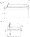
- FIG. 1A is a non-inventive modification of an optoelectronic semiconductor device 1 illustrated as a sectional view.
- the semiconductor component 1 comprises a semiconductor layer sequence 3 with an active layer 30.
- a radiation passage area 35 of the semiconductor layer sequence 3 exhibits a roughening to improve a light extraction from the semiconductor layer sequence 3.
- the active layer 30 of the semiconductor layer sequence 3 is set up to emit an ultraviolet, a near-infrared or a visible radiation, in particular blue light, during operation of the semiconductor component 1.
- the semiconductor layer sequence 3 may be based on GaN, InGaN, AlGaN, GaP, InGaAlP, InGaAs or GaAs.
- the metal mirror 4 is, for example, a silver mirror and is in direct contact with the semiconductor layer sequence 3.
- the semiconductor component 1 comprises a carrier 2.
- the carrier 2 includes a carrier substrate 23 which is made, for example, of a metal, a ceramic or of silicon or germanium.
- solder connection layers 22a, 22b adjoin the carrier substrate 23. At least one of the solder connection layers 22a, 22b is covered by the carrier 2 and applied to the carrier substrate 23.
- the solder connection layer 22a can be produced and / or applied to the semiconductor layer sequence 3.
- a metal layer 24 is located on a side of the carrier substrate 23 facing away from the semiconductor layer sequence 3. Via the metal layer 24, the semiconductor component 1 can be soldered, for example via surface mounting, to an external mounting carrier, not shown.
- the solder connection layer 22a and the semiconductor layer sequence 3 there is furthermore an encapsulation intermediate layer 21.
- the encapsulation intermediate layer 21 comprises or consists of TiWN.
- Both the carrier 2 and the semiconductor layer sequence 3 project beyond the metal mirror 4 in a lateral direction, preferably all around.
- the semiconductor layer sequence 3 and the carrier 2 project laterally beyond the metal mirror 4.
- the lateral boundary surfaces of the semiconductor layer sequence 3 represent, and at one of the metal mirror. 4 Uncovered, the carrier substrate 23 facing bottom of the semiconductor layer sequence 3 is an encapsulation layer 5.
- the encapsulation layer 5 is prepared by an atomic layer deposition method and preferably electrically insulating.
- a material of the encapsulation layer 5 preferably has a low refractive index in order to reflect a large proportion of radiation which strikes the encapsulation layer 5 via total reflection.
- Low refractive index may mean that the refractive index or the average refractive index of the encapsulation layer 5 is at most 1.7, preferably at most 1.6.
- the mean refractive index of the encapsulant layer is 5 ⁇ m at least 35% smaller than an average refractive index of the semiconductor layer sequence 3.
- a thickness of the semiconductor layer sequence 3 is preferably between 3 ⁇ m and 15 ⁇ m inclusive, in particular between 4 ⁇ m and 6 ⁇ m inclusive.
- the metal mirror 4 has a thickness of preferably between 100 nm and 150 nm inclusive.
- a thickness of the encapsulation layer 5 is according to FIG. 1 less than half of a thickness of the metal mirror 4, so that through the encapsulation layer 5 in the region in which the semiconductor layer sequence 3 and the carrier 2 laterally project beyond the metal mirror 4, a groove 7 is formed.
- the encapsulant layer 5 is then preferably between 30 nm and 70 nm thick.
- a thickness of the second mirror layer 6 is preferably between 50 nm and 250 nm inclusive.
- a thickness of the encapsulation intermediate layer 21 is, for example, between 200 nm and 1.5 ⁇ m inclusive.
- the solder bonding layers 22a, 22b, taken together, have, for example, a thickness of between 1 ⁇ m and 6 ⁇ m, and are formed or consist in particular of Au, Zn, Ni and / or In.
- the support substrate 23 preferably has a thickness of between 50 ⁇ m and 500 ⁇ m, in particular between 75 ⁇ m and 200 ⁇ m.
- the metallic contact layers 24, which are made of, for example, Au or an Au alloy, have, for example, a thickness of between 50 nm and 300 nm inclusive.
- the semiconductor device 1 can be produced as follows: On a not shown growth substrate is the Semiconductor layer sequence 3, for example epitaxially grown. Moreover, on a side of the semiconductor layer sequence 3 facing away from the growth substrate, the metal mirror 4 and the second mirror layer 6 are for example printed, vapor-deposited or deposited by a galvanic process. Furthermore, the encapsulation intermediate layer 21 is applied to the second mirror layer 6, on which in turn the solder connection layer 22a is produced.
- the carrier 2 with the solder connection layer 22 b, the carrier substrate 23 and the metallic contact layer 24 is provided. Before or even after a detachment of the semiconductor layer sequence 3 from the growth substrate, not shown, the solder connection layers 22a, 22b are soldered to each other, whereby the support 2 is firmly connected to the semiconductor layer sequence 3. Likewise, the carrier 2 may be applied galvanically to the semiconductor layer sequence 3.
- a mask for example in the form of a photoresist, is applied to the semiconductor layer sequence 3.
- the flanks 32 of the semiconductor layer sequence 3 are then produced by etching, for example, and the semiconductor layer sequence 3 is patterned in their lateral dimensions.
- the metal mirror 4 is then preferably structured with another etching method and its lateral dimensions are determined. As a result of this structuring, the supernatant of the semiconductor layer sequence 3 is generated via the metal mirror 4.
- a structuring of the Semiconductor layer sequence 3 and the metal mirror 4 is thus preferably carried out over the same mask in successive etching steps. For example, after removing the mask (not shown), the patterning on the radiation passage area 35 can then be generated.
- the encapsulation layer 5 is produced via an atomic layer deposition.
- the radiation passage area 35 preferably remains free from the encapsulation layer 5.
- the encapsulation layer 5 comprises one or more unselected individual layers with or made of a silicon dioxide and / or an aluminum oxide, wherein the layers each have a thickness between preferably including 2 nm and 8 nm and a Total thickness of the encapsulation layer 5 is preferably between 30 nm and 70 nm inclusive.
- individual layers of SiO 2 and Al 2 O 3 are arranged alternately.
- a lateral projection L of the semiconductor layer sequence 3 via the metal mirror 4 is preferably between 100 nm and 5 ⁇ m inclusive.
- the lateral projection L is preferably less than 1 ⁇ m or less than 0.5 ⁇ m.
- Such small protrusions L can be realized by structuring the semiconductor layer sequence 3 and the metal mirror 4 by means of the same mask, not shown, so that the structuring of the metal mirror and the semiconductor layer sequence 3 relative to each other takes place precisely.
- the encapsulation layer 5 is preferably transparent and absorbs an electromagnetic generated, for example, in the semiconductor layer sequence 3 Radiation not or only negligible. If the active layer is set up to generate radiation, a portion of the radiation generated in the active layer 30 can pass through the encapsulation layer 5 with little loss and be reflected back at the second mirror layer 6, for example in the direction of the radiation passage area 35. As a result, a coupling-out efficiency of the radiation from the semiconductor component 1 increases.
- FIG. 1B a detail view of the encapsulation layer 5 is shown. Furthermore, according to FIG. 1B applied to the encapsulation layer 5, a protective layer 50.
- a thickness of the protective layer 50 is, for example, between 100 nm and 400 nm inclusive.
- the protective layer 50 is made, for example, via CVD or PVD.
- a CVD or PVD is generally not able to completely fill the groove 7 with a material. In this way, in the area in which the semiconductor layer sequence 3 and the carrier 2 project laterally beyond the metal mirror 4, a cavity which is enclosed by the encapsulation layer 5 and the protective layer 50 remains behind.
- the encapsulation layer 5 formed by ALD and the protection layer 50 formed by CVD or PVD differ in that a defect density in the ALD encapsulation layer 5 is typically smaller than 0.1 defects per square millimeter, whereas the CVD or PVD protection layer 50 is one Defect density of some 100 defects per square millimeter. This is detectable, for example, by transmission electron microscopy, TEM for short. Due to the comparatively lower defect density of the ALD encapsulation layer 5, an etching rate is also reduced compared to the CVD or PVD protection layer 50. In particular, this is the case if the encapsulation layer 5 and the protective layer 50 consist of or comprise aluminum oxide. For example, on the defect density and / or the etching rate can be determined which of the layers 5, 50 was generated by which method.
- the encapsulation layer 5 has grown so thickly over ALD that a sub-layer grown from the semiconductor layer sequence 3 and a sub-layer of the encapsulation layer 5 grown from the second mirror layer 6 touch and form a seam 8. This ensures a particularly efficient encapsulation of the metal mirror 4 with respect to oxygen and / or water.
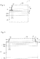
- FIG. 3 is a sectional view of a non-inventive modification of a semiconductor device illustrated.
- the metal mirror 4 is also surrounded in the lateral direction by the encapsulation intermediate layer 21.
- the encapsulation intermediate layer 21 consists, for example, of TiWN which exhibits a black or brownish coloration, then radiation generated in the semiconductor layer sequence 3, for example, is strongly absorbed at the encapsulation intermediate layer 21 and is not coupled out of the semiconductor component.
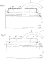
- FIG. 4 At the radiation passage surface 35, a bonding wire 9 is attached. An energization of the semiconductor device 1 then takes place via the metallic contact layer 24 and via the bonding wire 9.
- the semiconductor component 1 comprises two metallic contact layers 24, which are each guided via electrical plated-through holes 10 to a side of the carrier substrate 23 facing the semiconductor layer sequence 3.
- An electrical contacting of a side of the semiconductor layer sequence 3 facing the carrier substrate 23 furthermore takes place via the electrical bridge 12, which bridges a recess 15 in the solder connection layers 22a, 22b and in the encapsulation intermediate layer 21.
- a side facing away from the carrier substrate 23 of the semiconductor layer sequence is electrically connected via an opening 11, which is filled with copper, for example.
- the encapsulation layer 5 is, for example, as in FIGS Figures 1B or 2 shown executed.
- the semiconductor layer sequence 3 may be surrounded by a potting 14.
- the casting 14 can be at least one conversion means, at least one diffusion agent and / or at least one filter medium to be added.
- the carrier substrate 23 can optionally, as in the other examples, an integrated electrical functional element 13, which is designed for example as a protective device against electrostatic discharge.
- the encapsulation layer 5 completely or almost completely covers the radiation passage area 35, in particular with the exception of an optional connection area for the bonding wire 9.
- the encapsulation layer 5 consists of a material transparent to at least a portion of the radiation generated in the semiconductor layer sequence 3 or contains such a material.
- the encapsulant layer 5 then comprises or consists of silicon dioxide, wherein the silicon dioxide may be doped.
- a doping is carried out in particular with aluminum having a dopant concentration of preferably at most 1000 ppm or at most 100 ppm, where ppm stands for parts per million.
- the encapsulation layer 5 extends exclusively or essentially onto the groove 7. Unlike in FIG. 7 it is also possible for the encapsulation layer 5 to also partially extend to the flanks 32 of the semiconductor layer sequence 3, wherein the encapsulation layer 5, however, then does not reach the active layer 30 or, in a direction away from the carrier substrate 23, does not exceed. Likewise, parts of the encapsulation intermediate layer 21 located outside the groove 7 may also be covered by the encapsulation layer 5.
- the encapsulant layer 5 is made of one or more of the following materials: a transparent conductive oxide such as indium tin oxide, a pure metal such as tungsten.
- Such an encapsulation layer 5, as in FIG. 7 can be produced by a material for the encapsulation layer 5 is applied only in particular to the entire semiconductor layer sequence 3, similar to the embodiment according to FIG. 6 , and subsequently the material is removed in places.
Description
Es wird ein optoelektronisches Halbleiterbauteil angegeben. Darüber hinaus wird ein Verfahren zur Herstellung eines anorganischen optoelektronischen Halbleiterbauteils angegeben.An optoelectronic semiconductor component is specified. In addition, a method for producing an inorganic optoelectronic semiconductor device is specified.
Die Druckschrift
In der Druckschrift
Ein Schutz epitaktisch erzeugter Strukturen findet sich in der Druckschrift
Die Druckschrift
Aus der Druckschrift
Dass für die Herstellung von Schichten in Leuchtdioden Atomlagenabscheidung verwendbar ist, ergibt sich aus der Druckschrift
Eine zu lösende Aufgabe besteht darin, ein optoelektronisches Halbleiterbauteil mit einer hohen Lichtauskoppeleffizienz anzugeben. Eine weitere zu lösende Aufgabe besteht darin, ein Verfahren zur Herstellung eines solchen optoelektronischen Halbleiterbauteils anzugeben.An object to be solved is to specify an optoelectronic semiconductor component with a high light extraction efficiency. Another object to be solved is to specify a method for producing such an optoelectronic semiconductor component.
Diese Aufgabe wird gelöst durch ein Halbleiterbauteil und durch ein Verfahren mit den Merkmalen der unabhängigen Patentansprüche.This object is achieved by a semiconductor device and by a method having the features of the independent claims.
Das optoelektronische Halbleiterbauteil beinhaltet mindestens eine Halbleiterschichtenfolge. Bei der bevorzugt anorganischen Halbleiterschichtenfolge kann es sich um eine Leuchtdiode, um eine Laserdiode oder um eine Fotodiode handeln. Bevorzugt ist die Halbleiterschichtenfolge eine Dünnfilmschichtenfolge, wie beispielsweise in der Druckschrift
Das optoelektronische Halbleiterbauteil umfasst einen Träger. Der Träger ist bevorzugt dazu eingerichtet, die Halbleiterschichtenfolge zu tragen und mechanisch zu stützen. Bei dem Träger handelt es sich insbesondere um einen rigiden, im Rahmen der im verwendungsgemäßen Betrieb des Halbleiterbauteils auftretenden Belastungen biegestabilen Festkörper. Beispielsweise umfasst oder besteht der Träger aus einem Halbleitermaterial wie Germanium oder Silizium, aus einem Metall wie Cu, Ni, Ag oder Mo oder aus einem elektrisch isolierenden Material wie Al2O3, AlN oder SiNx. Der Träger kann von einem Aufwachssubstrat der Halbleiterschichtenfolge verschieden sein.The optoelectronic semiconductor component comprises a carrier. The carrier is preferably configured to carry and mechanically support the semiconductor layer sequence. The carrier is in particular a rigid, bending-resistant solid material in the context of the loads occurring in the operation according to the invention of the semiconductor component. For example, the support comprises or consists of a semiconductor material such as germanium or silicon, of a metal such as Cu, Ni, Ag or Mo or of an electrically insulating material such as Al 2 O 3 , AlN or SiN x . The carrier may be different from a growth substrate of the semiconductor layer sequence.
Es ist die Halbleiterschichtenfolge an dem Träger angebracht. Das kann bedeuten, dass sich zwischen der Halbleiterschichtenfolge und dem Träger eine oder mehrere Schichten befinden, über die eine Haftvermittlung und eine feste Verbindung zwischen der Halbleiterschichtenfolge und dem Träger gewährleistet ist. Insbesondere besteht kein unmittelbarer Kontakt zwischen einem Material des Trägers und der Halbleiterschichtenfolge.The semiconductor layer sequence is attached to the carrier. This may mean that there are one or more layers between the semiconductor layer sequence and the carrier, via which adhesion promotion and a firm connection between the semiconductor layer sequence and the carrier is ensured. In particular, there is no direct contact between a material of the carrier and the semiconductor layer sequence.
Das optoelektronische Halbleiterbauteil umfasst einen Metallspiegel. Der Metallspiegel befindet sich zwischen dem Träger und der Halbleiterschichtenfolge. Es ist der gesamte Metallspiegel so angeordnet, dass er sich vollständig zwischen der Halbleiterschichtenfolge und dem Träger befindet. Der Metallspiegel ist dazu eingerichtet, eine von der aktiven Schicht zu emittierende oder zu empfangende Strahlung zu reflektieren. Metallspiegel bedeutet, dass der Spiegel überwiegend oder vollständig aus einem Metall oder einer Metalllegierung besteht. Beispielsweise ist der Metallspiegel ein Silberspiegel. Eine elektrische Verbindung zwischen dem Träger und der Halbleiterschichtenfolge kann über den bevorzugt elektrisch leitfähigen Metallspiegel erfolgen. Der Metallspiegel kann in unmittelbarem Kontakt zu der Halbleiteschichtenfolge stehen.The optoelectronic semiconductor component comprises a metal mirror. The metal mirror is located between the carrier and the semiconductor layer sequence. The entire metal mirror is arranged so that it is completely between the semiconductor layer sequence and the carrier. The metal mirror is configured to reflect a radiation to be emitted or received by the active layer. Metal mirror means that the mirror consists mainly or completely of a metal or a metal alloy. For example, the metal mirror is a silver mirror. An electrical connection between the carrier and the semiconductor layer sequence can take place via the preferably electrically conductive metal mirror. The metal mirror may be in direct contact with the semiconductor layer sequence.
Insbesondere umfasst oder besteht der Metallspiegel aus einem Material, wie zum Beispiel Silber, das unter dem Einfluss von Sauerstoff oder von Wasser chemisch beschädigt wird. Auch kann ein Material des Metallspiegels, zum Beispiel ebenfalls Silber, zu einer Migration neigen, speziell unter dem Einfluss von Feuchtigkeit und/oder elektrischer Spannung.In particular, the metal mirror comprises or consists of a material, such as silver, which is chemically damaged under the influence of oxygen or water. Also, a material of the metal mirror, for example, too Silver, tend to migrate, especially under the influence of moisture and / or electrical voltage.
Es überragen der Träger und die Halbleiterschichtenfolge den Metallspiegel in einer lateralen Richtung. Die laterale Richtung ist zum Beispiel eine Richtung, die sich parallel entlang einer Haupterstreckungsrichtung des Trägers erstreckt. Insbesondere ist der Metallspiegel in jeder lateralen Richtung sowohl von dem Träger als auch von der Halbleiterschichtenfolge überragt. Mit anderen Worten stehen sowohl der Träger als auch die Halbleiterschichtenfolge in lateraler Richtung bevorzugt ringsum beziehungsweise allseitig über den Metallspiegel über.The carrier and the semiconductor layer sequence project beyond the metal mirror in a lateral direction. The lateral direction is, for example, a direction extending in parallel along a main extension direction of the carrier. In particular, the metal mirror in each lateral direction is surmounted by both the carrier and the semiconductor layer sequence. In other words, both the carrier and the semiconductor layer sequence in the lateral direction are preferably over the metal mirror all around or on all sides.
Es ist der Metallspiegel in lateraler Richtung unmittelbar von einer für eine von der Halbleiterschichtenfolge zu emittierende oder zu empfangende Strahlung durchlässigen und elektrisch isolierenden oder elektrisch leitfähigen Verkapselungsschicht umgeben. Mit anderen Worten grenzt ein Material der Verkapselungsschicht insbesondere ringsum direkt an ein Material des Metallspiegels, zum Beispiel an alle Begrenzungsflächen des Metallspiegels, die nicht dem Träger oder der Halbleiterschichtenfolge zugewandt sind.The metal mirror in the lateral direction is surrounded directly by a permeable and electrically insulating or electrically conductive encapsulation layer for a radiation to be emitted or received by the semiconductor layer sequence. In other words, a material of the encapsulation layer, in particular all around, directly adjoins a material of the metal mirror, for example all boundary surfaces of the metal mirror, which do not face the carrier or the semiconductor layer sequence.
Das optoelektronische Halbleiterbauteil beinhaltet einen Träger und mindestens eine Halbleiterschichtenfolge. Die Halbleiterschichtenfolge weist zumindest eine aktive Schicht auf. Die Halbleiterschichtenfolge ist ferner an dem Träger angebracht. Weiterhin beinhaltet das Halbleiterbauteil einen Metallspiegel, der sich zwischen dem Träger und der Halbleiterschichtenfolge befindet. Der Träger und die Halbleiterschichtenfolge überragen den Metallspiegel in lateraler Richtung. Außerdem ist der Metallspiegel in lateraler Richtung unmittelbar von einer strahlungsdurchlässigen und elektrisch isolierenden oder elektrisch leitfähigen Verkapselungsschicht umgeben.The optoelectronic semiconductor component includes a carrier and at least one semiconductor layer sequence. The semiconductor layer sequence has at least one active layer. The semiconductor layer sequence is further attached to the carrier. Furthermore, the semiconductor device includes a metal mirror, which is located between the carrier and the semiconductor layer sequence. The carrier and the semiconductor layer sequence project beyond the metal mirror in the lateral direction. Besides, the metal mirror is in Lateral direction directly surrounded by a radiation-transmissive and electrically insulating or electrically conductive encapsulation layer.
Dadurch, dass der Metallspiegel in lateraler Richtung von der Verkapselungsschicht insbesondere vollständig umgeben ist, so dass keine der Halbleiterschichtenfolge oder dem Träger zugewandte Begrenzungsfläche des Metallspiegels frei liegt, ist der Metallspiegel vor einer Beschädigung, beispielsweise durch Oxidation, schützbar. Auch kann eine Migration von Bestandteilen des Metallspiegels, zum Beispiel auf laterale Begrenzungsflächen der Halbleiterschichtenfolge, durch die Verkapselungsschicht verhindert oder stark reduziert werden. Durch die Verwendung einer strahlungsdurchlässigen Verkapselungsschicht ist eine Auskoppeleffizienz einer im Halbleiterbauteil beispielsweise erzeugten Strahlung steigerbar, da durch die Verkapselungsschicht im Wesentlichen keine Strahlung absorbiert wird und da insbesondere durch unter der Verkapselungsschicht liegende weitere Schichten eine effiziente Reflexion und Umlenkung der Strahlung erfolgen kann.Due to the fact that the metal mirror is in particular completely surrounded by the encapsulation layer in the lateral direction, so that no boundary surface of the metal mirror or the boundary surface of the metal mirror facing the support is exposed, the metal mirror can be protected against damage, for example by oxidation. Also, migration of components of the metal mirror, for example on lateral boundary surfaces of the semiconductor layer sequence, can be prevented or greatly reduced by the encapsulation layer. By using a radiation-permeable encapsulation layer, a coupling-out efficiency of a radiation generated in the semiconductor component, for example, is substantially absorbed, since substantially no radiation is absorbed by the encapsulation layer and, in particular, efficient reflection and deflection of the radiation can take place by further layers underlying the encapsulation layer.
Gemäß zumindest einer Ausführungsform des optoelektronischen Halbleiterbauteils weist ein Material der Verkapselungsschicht eine spezifische Diffusionskonstante für Wasser und/oder Sauerstoff von höchstens 10-5 g/(m2 d) auf. Die spezifische Diffusionskonstante ist hierbei insbesondere gerechnet auf eine Materialdicke von 0,1 µm. Bevorzugt beträgt die Diffusionskonstante höchstens 5 x 10⁻⁶ g/(m2 d), insbesondere höchstens 10-6 g/(m2 d). Durch ein solches Material für die Verkapselungsschicht ist eine Dicke der Verkapselungsschicht gering wählbar. Weiterhin kann ein solches Material für die Verkapselungsschicht gewährleisten, dass innerhalb einer Lebensdauer der Halbleiterschichtenfolge eine signifikante Korrosion oder chemische Zerstörung des Metallspiegels verhinderbar ist.According to at least one embodiment of the optoelectronic semiconductor component comprises a material of the encapsulation layer to a specific diffusion constant for water and / or oxygen of at most 10 -5 g / (m 2 d). The specific diffusion constant is in this case calculated in particular to a material thickness of 0.1 μm. The diffusion constant is preferably at most 5 × 10 -6 g / (m 2 d), in particular at most 10 -6 g / (m 2 d). By means of such a material for the encapsulation layer, a thickness of the encapsulation layer can be selected to be low. Furthermore, such a material can ensure the encapsulation layer that within a lifetime of the semiconductor layer sequence, significant corrosion or chemical destruction of the metal mirror can be prevented.
Gemäß zumindest einer Ausführungsform des optoelektronischen Halbleiterbauteils umfasst die Verkapselungsschicht oder besteht die Verkapselungsschicht aus einem Siliziumoxid, einem Aluminiumoxid und/oder einem Zirkoniumoxid. Ebenso kann die Verkapselungsschicht eines der folgenden Materialien umfassen oder hieraus bestehen: TiO2, HfO2, SnO2, SiC, Zr(SiO4), Pb3(Si2O7), Na(AlSiO4), Si3N4, AlN, GaN. Auch andere transparente, feuchtestabile Oxide, Carbide und/oder Nitride können für die Verkapselungsschicht Verwendung finden.In accordance with at least one embodiment of the optoelectronic semiconductor component, the encapsulation layer or the encapsulation layer comprises a silicon oxide, an aluminum oxide and / or a zirconium oxide. Likewise, the encapsulation layer may comprise or consist of one of the following materials: TiO 2 , HfO 2 , SnO 2 , SiC, Zr (SiO 4 ), Pb 3 (Si 2 O 7 ), Na (AlSiO 4 ), Si 3 N 4 , AlN, GaN. Other transparent, moisture-stable oxides, carbides and / or nitrides can be used for the encapsulation layer.
Gemäß zumindest einer Ausführungsform des optoelektronischen Halbleiterbauteils weist der Metallspiegel eine Dicke zwischen einschließlich 100 nm und 200 nm auf, insbesondere zwischen einschließlich 100 nm und 150 nm.According to at least one embodiment of the optoelectronic semiconductor component, the metal mirror has a thickness of between 100 nm and 200 nm, in particular between 100 nm and 150 nm inclusive.
Es liegt eine Dicke der Verkapselungsschicht zwischen einschließlich 20 nm und 100 nm, insbesondere zwischen einschließlich 35 nm und 70 nm. Die Dicke der Verkapselungsschicht ist hierbei insbesondere zu messen in einer Richtung parallel zu einer Wachstumsrichtung der Verkapselungsschicht. Weist die Verkapselungsschicht mehrere, zusammengewachsene Teilbereiche auf, so ist die Dicke insbesondere jeweils für die einzelnen Teilbereiche zu bestimmen, zum Beispiel bis hin zu einer Naht, an der die einzelnen Teilbereiche aneinander grenzen.A thickness of the encapsulation layer is between 20 nm and 100 nm inclusive, in particular between 35 nm and 70 nm inclusive. In this case, the thickness of the encapsulation layer is to be measured in particular in a direction parallel to a growth direction of the encapsulation layer. If the encapsulation layer has a plurality of coalesced subareas, the thickness must be determined in each case for the individual subregions, for example, up to a seam at which the individual subareas adjoin one another.
Das optoelektronische Halbleiterbauteil umfasst eine zweite Spiegelschicht, die sich zwischen dem Metallspiegel und dem Träger befindet. Die zweite Spiegelschicht grenzt hierbei bevorzugt unmittelbar an den Metallspiegel, so dass ein Material der zweiten Spiegelschicht in physischem Kontakt mit einem Material des Metallspiegels steht. Die zweite Spiegelschicht ist elektrisch leitend und beispielsweise ebenfalls aus zumindest einem Metall geformt. Ein Material der zweiten Spiegelschicht ist beispielsweise Cr oder eine Cr-Legierung. Weitere mögliche Materialien für die zweite Spiegelschicht sind Ti, Ti3N4, TiW, TiW(N), Au, Pt, Pd und/oder Ni. Bevorzugt neigt das Material der zweiten Spiegelschicht nicht oder zumindest weniger stark als das Material der Verkapselungsschicht zu Migration und Korrosion unter dem Einfluss von Feuchtigkeit und/oder Sauerstoff.The optoelectronic semiconductor device comprises a second mirror layer which extends between the metal mirror and the Carrier is located. In this case, the second mirror layer preferably directly adjoins the metal mirror so that a material of the second mirror layer is in physical contact with a material of the metal mirror. The second mirror layer is electrically conductive and, for example, also formed from at least one metal. A material of the second mirror layer is, for example, Cr or a Cr alloy. Further possible materials for the second mirror layer are Ti, Ti 3 N 4 , TiW, TiW (N), Au, Pt, Pd and / or Ni. Preferably, the material of the second mirror layer does not tend, or at least less strongly, than the material of the encapsulation layer to migration and corrosion under the influence of moisture and / or oxygen.
Es überragt die zweite Spiegelschicht den Metallspiegel in lateraler Richtung ringsum. Ebenso bevorzugt überragt die zweite Spiegelschicht die Verkapselungsschicht in lateraler Richtung, insbesondere ringsum.It towers over the second mirror layer the metal mirror in a lateral direction all around. The second mirror layer likewise preferably projects beyond the encapsulation layer in the lateral direction, in particular all the way around.
Die zweite Spiegelschicht ist dazu eingerichtet, eine durch die Verkapselungsschicht transmittierte, in der aktiven Schicht erzeugte elektromagnetische Strahlung zu reflektieren. Mit anderen Worten wird die auf die Verkapselungsschicht treffende Strahlung mindestens teilweise speziell durch die Verkapselungsschicht transmittiert, von der zweiten Spiegelschicht reflektiert und zum Beispiel hin zu einer Strahlungsdurchtrittsfläche der Halbleiterschichtenfolge gelenkt. Die Strahlungsdurchtrittsfläche ist eine dem Träger abgewandte Begrenzungsfläche der Halbleiterschichtenfolge.The second mirror layer is configured to reflect an electromagnetic radiation transmitted through the encapsulation layer and generated in the active layer. In other words, the radiation striking the encapsulation layer is at least partially transmitted in particular by the encapsulation layer, reflected by the second mirror layer and, for example, directed toward a radiation passage area of the semiconductor layer sequence. The radiation passage area is a boundary surface of the semiconductor layer sequence facing away from the carrier.
Gemäß zumindest einer Ausführungsform des optoelektronischen Halbleiterbauteils emittiert dieses einen überwiegenden Teil der Strahlung, zum Beispiel mehr als 50 % oder mehr als 80 %, an der dem Träger abgewandten Strahlungsdurchtrittsfläche. Mit anderen Worten kann eine Hauptabstrahlungsrichtung der in dem Halbleiterbauteil erzeugten Strahlung senkrecht zu einer durch Hauptserstreckungsrichtungen der aktiven Schicht aufgespannten Ebene, also insbesondere senkrecht zu einer Seite des Trägersubstrats, auf das die Halbleiterschichtenfolge aufgebracht ist, oder parallel zu einer Wachstumsrichtung der Halbleiterschichtenfolge, orientiert sein.According to at least one embodiment of the optoelectronic semiconductor device, this emits a predominant part the radiation, for example, more than 50% or more than 80%, at the radiation passage surface facing away from the carrier. In other words, a main emission direction of the radiation generated in the semiconductor component can be oriented perpendicular to a plane spanned by main extension directions of the active layer, ie, in particular perpendicular to one side of the carrier substrate to which the semiconductor layer sequence is applied, or parallel to a growth direction of the semiconductor layer sequence.
Es ist die Verkapselungsschicht im Querschnitt U-förmig geformt. Schenkel des U's weisen weg von dem Metallspiegel, das heißt, eine offene Seite des U's ist dem Metallspiegel abgewandt. Mit anderen Worten ist durch die Verkapselungsschicht, insbesondere in dem Bereich, in dem die Halbleiterschichtenfolge und der Träger den Metallspiegel lateral überragen, eine Art Hohlkehle gebildet. Das heißt, die Verkapselungsschicht schmiegt sich an die über den Metallspiegel überstehenden Bereiche der Halbleiterschichtenfolge und des Trägers oder der zweiten Spiegelschicht oder einer Lotverbindungsschicht sowie an die lateralen Begrenzungsflächen des Metallspiegels an, wobei in dem Überstandbereich ein Hohlraum in Richtungen senkrecht zur lateralen Richtung von der Verkapselungsschicht begrenzt ist.It is the encapsulation layer in cross-section U-shaped. Legs of the U point away from the metal mirror, that is, an open side of the U is facing away from the metal mirror. In other words, a kind of groove is formed by the encapsulation layer, in particular in the region in which the semiconductor layer sequence and the support project laterally beyond the metal mirror. That is, the encapsulation layer conforms to the regions of the semiconductor layer sequence projecting beyond the metal mirror and the carrier or the second mirror layer or a solder connection layer and to the lateral boundary surfaces of the metal mirror, wherein in the overhang region a cavity in directions perpendicular to the lateral direction of the encapsulation layer is limited.
Gemäß zumindest einer Ausführungsform des optoelektronischen Halbleiterbauteils umfasst die Verkapselungsschicht eine Folge von Einzelschichten, wobei mindestens zwei der Einzelschichten ein voneinander verschiedenes Material beinhalten. Beispielsweise weist die Verkapselungsschicht eine alternierende Folge von Einzelschichten von zumindest zwei verschiedenen Materialien auf. Bevorzugt umfasst die Verkapselungsschicht mindestens vier Einzelschichten, bevorzugt mindestens acht Einzelschichten, insbesondere mindestens zwölf Einzelschichten.In accordance with at least one embodiment of the optoelectronic semiconductor component, the encapsulation layer comprises a sequence of individual layers, wherein at least two of the individual layers comprise a mutually different material. For example, the encapsulation layer has an alternating sequence of individual layers of at least two different materials. Preferably, the Encapsulation layer at least four individual layers, preferably at least eight individual layers, in particular at least twelve individual layers.
Gemäß zumindest einer Ausführungsform des optoelektronischen Halbleiterbauteils beträgt eine Dicke der Einzelschichten jeweils zwischen einschließlich 2 nm und 8 nm, insbesondere zwischen einschließlich 3 nm und 6 nm.In accordance with at least one embodiment of the optoelectronic semiconductor component, a thickness of the individual layers is in each case between 2 nm and 8 nm inclusive, in particular between 3 nm and 6 nm inclusive.
Gemäß zumindest einer Ausführungsform des optoelektronischen Halbleiterbauteils beträgt ein lateraler Überstand der Halbleiterschichtenfolge über den Metallspiegel zwischen einschließlich 50 nm und 2,0 µm. Bevorzugt liegt der laterale Überstand zwischen einschließlich 100 nm und 1,0 µm, insbesondere zwischen einschließlich 100 nm und 500 nm.According to at least one embodiment of the optoelectronic semiconductor component, a lateral projection of the semiconductor layer sequence over the metal mirror is between 50 nm and 2.0 μm inclusive. The lateral supernatant is preferably between 100 nm and 1.0 μm, in particular between 100 nm and 500 nm inclusive.
Gemäß zumindest einer Ausführungsform des optoelektronischen Halbleiterbauteils ist die Verkapselungsschicht transparent. Eine die Verkapselungsschicht durchlaufende sichtbare Strahlung wird insbesondere zu höchstens 3,0 % absorbiert, bevorzugt zu höchstens 2,0 %. Mit anderen Worten weist die Verkapselungsschicht eine hohe Transparenz auf. Dies ist bevorzugt für solche Spektralbereiche der Fall, in denen von der Halbleiterschichtenfolge im Betrieb des Halbleiterbauteils eine elektromagnetische Strahlung erzeugt wird.In accordance with at least one embodiment of the optoelectronic semiconductor component, the encapsulation layer is transparent. A visible radiation passing through the encapsulation layer is in particular absorbed to a maximum of 3.0%, preferably to a maximum of 2.0%. In other words, the encapsulation layer has a high transparency. This is preferably the case for spectral regions in which an electromagnetic radiation is generated by the semiconductor layer sequence during operation of the semiconductor device.
Gemäß zumindest einer Ausführungsform des optoelektronischen Halbleiterbauteils beträgt ein Verhältnis aus einer Fläche des Metallspiegels und einer Fläche der Halbleiterschichtenfolge, gesehen in Draufsicht auf das Halbleiterbauteil, mindestens 95 %, bevorzugt mindestens 97 %, insbesondere mindestens 98,5 %. Mit anderen Worten ist im Wesentlichen die gesamte, dem Träger zugewandte Seite der Halbleiterschichtenfolge von dem Metallspiegel bedeckt.In accordance with at least one embodiment of the optoelectronic semiconductor component, a ratio of an area of the metal mirror and a surface of the semiconductor layer sequence, as seen in plan view of the semiconductor component, is at least 95%, preferably at least 97%, in particular at least 98.5%. In other words essentially covers the entire, the carrier-facing side of the semiconductor layer sequence of the metal mirror.
Gemäß zumindest einer Ausführungsform des optoelektronischen Halbleiterbauteils ist die Strahlungsdurchtrittsfläche der Halbleiterschichtenfolge frei von der Verkapselungsschicht.In accordance with at least one embodiment of the optoelectronic semiconductor component, the radiation passage area of the semiconductor layer sequence is free of the encapsulation layer.
Gemäß zumindest einer Ausführungsform des optoelektronischen Halbleiterbauteils ist die Strahlungsdurchtrittsfläche der Halbleiterschichtenfolge von der Verkapselungsschicht bedeckt. Zum Beispiel ist die Strahlungsdurchtrittsfläche von der Verkapselungsschicht, alleine oder zusammen mit einer elektrischen Kontaktstelle an der Strahlungsdurchtrittsfläche, vollständig bedeckt. Ein Material der Verkapselungsschicht ist dann bevorzugt SiO2.In accordance with at least one embodiment of the optoelectronic semiconductor component, the radiation passage area of the semiconductor layer sequence is covered by the encapsulation layer. For example, the radiation passage area of the encapsulation layer, alone or together with an electrical contact point at the radiation passage area, is completely covered. A material of the encapsulation layer is then preferably SiO 2 .
Gemäß zumindest einer Ausführungsform des optoelektronischen Halbleiterbauteils bedeckt die Verkapselungsschicht alle lateralen Begrenzungsflächen des Metallspiegels, eine dem Träger zugewandte, den Metallspiegel überragende Begrenzungsfläche der Halbleiterschichtenfolge, Flanken der Halbleiterschichtenfolge sowie eine der Halbleiterschichtenfolge zugewandte und von dieser in Draufsicht auf die Strahlungsdurchtrittsfläche überdeckte Begrenzungsfläche des Trägers, der zweiten Spiegelschicht und/oder einer Lotverbindungsschicht teilweise oder, bevorzugt, vollständig.In accordance with at least one embodiment of the optoelectronic semiconductor component, the encapsulation layer covers all lateral boundary surfaces of the metal mirror, a boundary surface of the semiconductor layer sequence facing the substrate, flanks of the semiconductor layer sequence and a boundary surface of the substrate facing the semiconductor layer sequence and covered by the latter in plan view onto the radiation passage area second mirror layer and / or a Lotverbindungsschicht partially or, preferably, completely.
Es wird darüber hinaus ein Verfahren zur Herstellung eines anorganischen optoelektronischen Halbleiterbauteils angegeben. Es ist mittels des Verfahrens ein Halbleiterbauteil hergestellt, wie in Verbindung mit einer oder mehrerer der oben genannten Ausführungsformen beschrieben. Merkmale des optoelektronischen Halbleiterbauteils sind daher auch für das hier beschriebene Verfahren offenbart und umgekehrt.In addition, a method for producing an inorganic optoelectronic semiconductor component is specified. A semiconductor device is manufactured by the method as in connection with one or more of the above-mentioned embodiments described. Features of the optoelectronic semiconductor device are therefore also disclosed for the method described here and vice versa.
Das Verfahren zur Herstellung des anorganischen optoelektronischen Halbleiterbauteils umfasst die Schritte:
- Bereitstellen eines Trägers, einer Halbleiterschichtenfolge und eines Metallspiegels, wobei sich der Metallspiegel zwischen dem Träger und der Halbleiterschichtenfolge befindet und von diesen in lateraler Richtung überragt wird,
- Aufbringen einer strahlungsdurchlässigen, elektrisch isolierenden oder elektrisch leitfähigen Verkapselungsschicht in lateraler Richtung unmittelbar an dem Metallspiegel, wobei die Verkapselungsschicht über eine Atomlagenabscheidung erzeugt wird, und
- Fertigstellen des optoelektronischen Halbleiterbauteils.
- Providing a carrier, a semiconductor layer sequence and a metal mirror, wherein the metal mirror is located between the carrier and the semiconductor layer sequence and is projected therefrom in the lateral direction,
- Applying a radiation-transmissive, electrically insulating or electrically conductive encapsulation layer in the lateral direction directly to the metal mirror, wherein the encapsulation layer is produced via an atomic layer deposition, and
- Completing the optoelectronic semiconductor device.
Die Halbleiterschichtenfolge wird beispielsweise durch ein epitaktisches Wachsen auf einem Aufwachssubstrat erzeugt. Der Träger ist bevorzugt von dem Aufwachssubstrat verschieden.The semiconductor layer sequence is produced for example by epitaxial growth on a growth substrate. The support is preferably different from the growth substrate.
Die Verkapselungsschicht kann über eine Atomlagenabscheidung analog zu der in der Druckschrift
Dadurch, dass die Verkapselungsschicht über eine Atomlagenabscheidung, englisch Atomic Layer Deposition oder kurz ALD, erzeugt wird, lässt sich eine besonders gleichmäßig gestaltete, nur vergleichsweise wenige Verunreinigungen und Defekte aufweisende und daher besonders diffusionsbeständige Schicht erzeugen.Due to the fact that the encapsulation layer is produced by an atomic layer deposition, abbreviated to ALD, it is possible to produce a layer which is particularly uniformly shaped and has only comparatively few impurities and defects and therefore is particularly diffusion-resistant.
Gemäß zumindest einer Ausführungsform des Verfahrens wird auf die Verkapselungsschicht vollständig oder stellenweise eine Schutzschicht über eine Gasphasenabscheidung aufgebracht, insbesondere auf solche Begrenzungsflächen der Verkapselungsschicht, die nicht an den Träger, die Halbleiterschichtenfolge, die zweite Spiegelschicht und/oder eine Lotverbindungsschicht grenzen. Bei der Gasphasenabscheidung kann es sich um eine so genannte Chemical Vapour Deposition, kurz CVD, oder um eine Physical Vapour Deposition, kurz PVD, handeln.In accordance with at least one embodiment of the method, a protective layer is completely or locally applied to the encapsulation layer via a vapor deposition, in particular to those boundary surfaces of the encapsulation layer which do not adjoin the carrier, the semiconductor layer sequence, the second mirror layer and / or a solder connection layer. The vapor deposition may be a so-called Chemical Vapor Deposition, CVD for short, or a Physical Vapor Deposition, PVD for short.
Gemäß zumindest einer Ausführungsform des Verfahrens wird die Schutzschicht mit einer Dicke zwischen einschließlich 100 nm und 500 nm erzeugt. Durch die Schutzschicht ist ein Schutz der Verkapselungsschicht insbesondere gegenüber mechanischen Belastungen und Beschädigungen erreichbar oder auch gegenüber Chemikalien, die reaktiv gegenüber einem Material der Verkapselungsschicht sind.In accordance with at least one embodiment of the method, the protective layer is produced with a thickness of between 100 nm and 500 nm inclusive. The protective layer makes it possible to protect the encapsulation layer, in particular against mechanical stresses and damage, or even against chemicals which are reactive with respect to a material of the encapsulation layer.
Gemäß zumindest einer Ausführungsform des Verfahrens erfolgt ein Strukturieren der Halbleiterschichtenfolge und des Metallspiegels mittels derselben Maske und insbesondere mittels eines Ätzens. Auf die Halbleiterschichtenfolge wird eine Maske über beispielsweise ein fotolithographisches Verfahren aufgebracht. Nachfolgend werden Flanken der Halbleiterschichtenfolge, also laterale Begrenzungsflächen der Halbleiterschichtenfolge, erzeugt. Ohne die Maske zu entfernen wird in einem nachfolgenden, insbesondere von einem ersten Ätzschritt verschiedenen zweiten Ätzschritt dann der Metallspiegel strukturiert, wobei ein Überstand der Halbleiterschichtenfolge in einer lateralen Richtung über den Metallspiegel erzielbar und einstellbar ist. Dadurch, dass beide Strukturierungsprozesse mit derselben Maske erfolgen, ist eine hohe Einstellgenauigkeit bezüglich der Formgebung der Halbleiterschichtenfolge relativ zu der Formgebung des Metallspiegels gewährleistet.According to at least one embodiment of the method, the semiconductor layer sequence and the metal mirror are patterned by means of the same mask and in particular by means of an etching. On the semiconductor layer sequence, a mask is applied via, for example, a photolithographic process. Subsequently, flanks of the semiconductor layer sequence, ie lateral boundary surfaces of the semiconductor layer sequence, are generated. Without removing the mask, in a subsequent second etching step, which is different in particular from a first etching step, the metal mirror is then patterned, wherein a supernatant of the semiconductor layer sequence can be achieved and adjusted in a lateral direction via the metal mirror. Because both structuring processes take place with the same mask, a high setting accuracy with respect to the shaping of the semiconductor layer sequence relative to the shape of the metal mirror is ensured.
Nachfolgend wird ein hier beschriebenes optoelektronisches Halbleiterbauteil sowie ein hier beschriebenes Verfahren unter Bezugnahme auf die Zeichnung näher erläutert. Gleiche Bezugszeichen geben dabei gleiche Elemente in den einzelnen Figuren an. Es sind dabei jedoch keine maßstäblichen Bezüge dargestellt, vielmehr können einzelne Elemente zum besseren Verständnis übertrieben groß dargestellt sein.Hereinafter, an optoelectronic semiconductor device described herein and a method described herein will be explained in more detail with reference to the drawings. The same reference numerals indicate the same elements in the individual figures. However, there are no scale relationships shown, but individual elements can be shown exaggerated for better understanding.
Es zeigen:
Figur 6- eine schematische Schnittdarstellung eines Ausführungsbeispiels eines hier beschriebenen optoelektronischen Halbleiterbauteils, und
Figuren - schematische Schnittdarstellungen von nicht erfindungsgemäßen Abwandlungen von optoelektronischen Halbleiterbauteilen.
- FIG. 6
- a schematic sectional view of an embodiment of an optoelectronic semiconductor device described herein, and
- FIGS. 1A, 1B, 2, 3, 4, 5 and 7
- schematic sectional views of non-inventive modifications of optoelectronic semiconductor devices.
In
Beispielsweise ist die aktive Schicht 30 der Halbleiterschichtenfolge 3 dazu eingerichtet, im Betrieb des Halbleiterbauteils 1 eine ultraviolette, eine nahinfrarote oder eine sichtbare Strahlung, insbesondere blaues Licht, zu emittieren. Die Halbleiterschichtenfolge 3 kann auf GaN, InGaN, AlGaN, GaP, InGaAlP, InGaAs oder GaAs basieren.By way of example, the
An einer der Strahlungsdurchtrittsfläche 35 abgewandten Seite der Halbleiterschichtenfolge 3 befindet sich ein Metallspiegel 4. Der Metallspiegel 4 ist zum Beispiel ein Silberspiegel und steht in unmittelbarem Kontakt mit der Halbleiterschichtenfolge 3.On a side of the
Ferner umfasst das Halbleiterbauteil 1 einen Träger 2. Der Träger 2 beinhaltet ein Trägersubstrat 23, das beispielsweise aus einem Metall, einer Keramik oder aus Silizium oder Germanium gefertigt ist. In einer Richtung hin zu der Halbleiterschichtenfolge 3 grenzen an das Trägersubstrat 23 Lotverbindungsschichten 22a, 22b. Mindestens eine der Lotverbindungsschichten 22a, 22b ist von dem Träger 2 umfasst und auf das Trägersubstrat 23 aufgebracht. Insbesondere die Lotverbindungsschicht 22a kann an der Halbleiterschichtenfolge 3 erzeugt und/oder aufgebracht sein. An einer der Halbleiterschichtenfolge 3 abgewandten Seite des Trägersubstrats 23 befindet sich ferner eine Metallschicht 24. Über die Metallschicht 24 ist das Halbleiterbauteil 1 beispielsweise über eine Oberflächenmontage an einen externen, nicht gezeichneten Montageträger lötbar.Furthermore, the
Zwischen der Lotverbindungsschicht 22a und der Halbleiterschichtenfolge 3 befindet sich weiterhin eine Kapselungszwischenschicht 21. Über die Kapselungszwischenschicht 21 ist eine Migration von Bestandteilen zum Beispiel der Lotverbindungsschichten 22a, 22b in die Halbleiterschichtenfolge 3 hinein unterbindbar. Beispielsweise umfasst die Kapselungszwischenschicht 21 TiWN oder besteht hieraus. Zwischen dem Metallspiegel 4 und der Kapselungszwischenschicht 21 befindet sich ferner eine zweite Spiegelschicht 6, die elektrisch leitend und beispielsweise aus Chrom gebildet ist.Between the
Sowohl der Träger 2 als auch die Halbleiterschichtenfolge 3 überragen in einer lateralen Richtung, bevorzugt ringsum, den Metallspiegel 4. Mit anderen Worten stehen die Halbleiterschichtenfolge 3 und der Träger 2 seitlich über den Metallspiegel 4 über. An lateralen Begrenzungsflächen des Metallspiegels 4, an einer der Halbleiterschichtenfolge 3 zugewandten Oberseite der zweiten Spiegelschicht 6, die nicht von dem Metallspiegel 4 bedeckt ist, optional an Flanken 32 der Halbleiterschichtenfolge 3, die laterale Begrenzungsflächen der Halbleiterschichtenfolge 3 darstellen, sowie an einer vom Metallspiegel 4 nicht bedeckten, dem Trägersubstrat 23 zugewandten Unterseite der Halbleiterschichtenfolge 3 befindet sich eine Verkapselungsschicht 5. Die Verkapselungsschicht 5 ist über ein Atomlagenabscheidungsverfahren hergestellt und bevorzugt elektrisch isolierend.Both the
Bevorzugt weist ein Material der Verkapselungsschicht 5 einen geringen Brechungsindex auf, um einen großen Anteil einer Strahlung, die auf die Verkapselungsschicht 5 trifft, über Totalreflexion zu reflektieren. Geringer Brechungsindex kann bedeuten, dass der Brechungsindex oder der mittlere Brechungsindex der Verkapselungsschicht 5 höchstens 1,7, bevorzugt höchstens 1,6 beträgt. Insbesondere ist der mittlere Brechungsindex der Verkapselungsschicht 5 um mindestens 35 % kleiner als ein mittlerer Brechungsindex der Halbleiterschichtenfolge 3.A material of the
Die Bestandteile des Halbleiterbauteils können, einzeln oder in Kombination, wie nachfolgend angegeben geformt sein. Eine Dicke der Halbleiterschichtenfolge 3 beträgt bevorzugt zwischen einschließlich 3 µm und 15 µm, insbesondere zwischen einschließlich 4 µm und 6 µm. Der Metallspiegel 4 weist eine Dicke von bevorzugt zwischen einschließlich 100 nm und 150 nm auf. Eine Dicke der Verkapselungsschicht 5 beträgt gemäß
Eine Dicke der zweiten Spiegelschicht 6 liegt bevorzugt zwischen einschließlich 50 nm und 250 nm. Eine Dicke der Kapselungszwischenschicht 21 beträgt beispielsweise zwischen einschließlich 200 nm und 1,5 µm. Die Lotverbindungsschichten 22a, 22b weisen, zusammengenommen, zum Beispiel eine Dicke zwischen einschließlich 1 µm und 6 µm auf und sind insbesondere mit Au, Zn, Ni und/oder In gebildet oder bestehen hieraus. Das Trägersubstrat 23 zeigt eine Dicke bevorzugt zwischen einschließlich 50 µm und 500 µm, insbesondere zwischen einschließlich 75 µm und 200 µm auf. Die metallischen Kontaktschichten 24, die beispielsweise aus Au oder einer Au-Legierung bestehen, haben zum Beispiel eine Dicke zwischen einschließlich 50 nm und 300 nm.A thickness of the
Das Halbleiterbauteil 1 kann wie folgt hergestellt werden: Auf einem nicht gezeichneten Aufwachssubstrat wird die Halbleiterschichtenfolge 3 beispielsweise epitaktisch aufgewachsen. Außerdem werden an einer dem Aufwachssubstrat abgewandten Seite der Halbleiterschichtenfolge 3 der Metallspiegel 4 und die zweite Spiegelschicht 6 beispielsweise aufgedruckt, aufgedampft oder über ein galvanisches Verfahren abgeschieden. Ferner wird an der zweiten Spiegelschicht 6 die Kapselungszwischenschicht 21 aufgebracht, an der wiederum die Lotverbindungsschicht 22a erzeugt wird.The
Weiterhin wird der Träger 2 mit der Lotverbindungsschicht 22b, dem Trägersubstrat 23 und der metallischen Kontaktschicht 24 bereitgestellt. Vor oder auch nach einem Ablösen der Halbleiterschichtenfolge 3 von dem nicht dargestellten Aufwachssubstrat werden die Lotverbindungsschichten 22a, 22b miteinander verlötet, wodurch der Träger 2 fest mit der Halbleiterschichtenfolge 3 verbunden wird. Ebenso kann der Träger 2 galvanisch an der Halbleiterschichtenfolge 3 aufgebracht sein.Furthermore, the
Insbesondere nach dem Entfernen des Aufwachssubstrats von der Halbleiterschichtenfolge 3 wird auf der Halbleiterschichtenfolge 3 eine nicht gezeichnete Maske, beispielsweise in Form eines Fotolacks, aufgebracht. Über zum Beispiel ein Ätzen werden dann die Flanken 32 der Halbleiterschichtenfolge 3 erzeugt und die Halbleiterschichtenfolge 3 in ihren lateralen Ausdehnungen strukturiert. Ohne die nicht gezeichnete Maske zu entfernen, wird mit einem anderen Ätzverfahren bevorzugt anschließend der Metallspiegel 4 strukturiert und dessen laterale Abmessungen bestimmt. Durch diese Strukturierung wird der Überstand der Halbleiterschichtenfolge 3 über den Metallspiegel 4 erzeugt. Eine Strukturierung der Halbleiterschichtenfolge 3 sowie des Metallspiegels 4 erfolgt also bevorzugt über dieselbe Maske in aufeinander folgenden Ätzschritten. Zum Beispiel nach dem Entfernen der nicht dargestellten Maske kann dann die Strukturierung an der Strahlungsdurchtrittsfläche 35 erzeugt werden.In particular, after the removal of the growth substrate from the
Vor oder auch nach dem Erzeugen der Strukturierung an der Strahlungsdurchtrittsfläche 35 wird die Verkapselungsschicht 5 über eine Atomlagenabscheidung erzeugt. Die Strahlungsdurchtrittsfläche 35 bleibt dabei bevorzugt frei von der Verkapselungsschicht 5. Die Verkapselungsschicht 5 umfasst eine oder mehrere nicht gezeichnete Einzelschichten mit oder aus einem Siliziumdioxid und/oder einem Aluminiumoxid, wobei die Lagen jeweils eine Dicke zwischen bevorzugt einschließlich 2 nm und 8 nm aufweisen und eine Gesamtdicke der Verkapselungsschicht 5 bevorzugt zwischen einschließlich 30 nm und 70 nm beträgt. Beispielsweise sind Einzelschichten aus SiO2 sowie Al2O3 abwechselnd angeordnet.Before or even after the structuring has been produced on the
Ein lateraler Überstand L der Halbleiterschichtenfolge 3 über den Metallspiegel 4 beträgt bevorzugt zwischen einschließlich 100 nm und 5 µm. Bevorzugt ist der laterale Überstand L kleiner als 1 µm oder kleiner als 0,5 µm. Derart kleine Überstände L sind dadurch realisierbar, dass eine Strukturierung der Halbleiterschichtenfolge 3 sowie des Metallspiegels 4 mittels derselben nicht dargestellten Maske erfolgt, so dass die Strukturierungen des Metallspiegels sowie der Halbleiterschichtenfolge 3 relativ zueinander präzise erfolgt.A lateral projection L of the
Ferner ist die Verkapselungsschicht 5 bevorzugt transparent und absorbiert eine zum Beispiel in der Halbleiterschichtenfolge 3 erzeugte elektromagnetische Strahlung nicht oder nur vernachlässigbar. Ist die aktive Schicht zur Erzeugung einer Strahlung eingerichtet, so kann ein Teil der in der aktiven Schicht 30 erzeugten Strahlung die Verkapselungsschicht 5 verlustarm durchlaufen und an der zweiten Spiegelschicht 6 zurück, zum Beispiel in Richtung zur Strahlungsdurchtrittsfläche 35, reflektiert werden. Hierdurch erhöht sich eine Auskoppeleffizienz der Strahlung aus dem Halbleiterbauteil 1.Furthermore, the
In
Im Gegensatz zur durch ein Atomlagenabscheiden, kurz ALD, erzeugten Verkapselungsschicht 5 ist die Schutzschicht 50 beispielsweise über CVD oder PVD erstellt. Im Gegensatz zu der ALD, über die die Verkapselungsschicht 5 hergestellt ist, ist eine CVD oder PVD im Regelfall nicht in der Lage, die Hohlkehle 7 mit einem Material vollständig auszufüllen. Hierdurch verbleibt in dem Bereich, in dem die Halbleiterschichtenfolge 3 und der Träger 2 lateral über dem Metallspiegel 4 überstehen, ein Hohlraum zurück, der von der Verkapselungsschicht 5 und der Schutzschicht 50 umschlossen ist.In contrast to the
Ferner unterscheiden sich die durch ALD erstellte Verkapselungsschicht 5 und die über CVD oder PVD erzeugte Schutzschicht 50 dadurch, dass eine Defektdichte bei der ALD-Verkapselungsschicht 5 typisch kleiner als 0,1 Defekte pro Quadratmillimeter beträgt, wohingegen die CVD- oder PVD-Schutzschicht 50 eine Defektdichte von einigen 100 Defekten pro Quadratmillimeter aufweist. Dies ist beispielsweise über Transmissionselektronenmikroskopie, kurz TEM, nachweisbar. Aufgrund der vergleichsweise geringeren Defektdichte der ALD-Verkapselungsschicht 5 ist auch eine Ätzrate, im Vergleich zur CVD- oder PVD-Schutzschicht 50, reduziert. Insbesondere ist dies der Fall, falls die Verkapselungsschicht 5 und die Schutzschicht 50 aus Aluminiumoxid bestehen oder dieses umfassen. Beispielsweise über die Defektdichte und/oder die Ätzrate ist feststellbar, welche der Schichten 5, 50 über welche Methode erzeugt wurde.Furthermore, the
Bei der nicht erfindungsgemäßen Abwandlung gemäß
In
Gemäß der nicht erfindungsgemäßen Abwandlung nach
Bei der nicht erfindungsgemäßen Abwandlung gemäß
Wie auch bei allen anderen Beispielen kann die Halbleiterschichtenfolge 3 von einem Verguss 14 umgeben sein. Dem Verguss 14 kann mindestens ein Konversionsmittel, mindestens ein Diffusionsmittel und/oder mindestens ein Filtermittel beigegeben sein. Dem Trägersubstrat 23 kann optional, wie auch bei den anderen Beispielen, ein elektrisches Funktionselement 13 integriert sein, das beispielsweise als Schutzvorrichtung vor elektrostatischer Entladung ausgeführt ist.As with all other examples, the
Gemäß dem Ausführungsbeispiel in
Bei der nicht erfindungsgemäßen Abwandlung gemäß
Insbesondere bei einer derartigen Ausformung der Verkapselungsschicht 5 ist es möglich, für die Verkapselungsschicht 5 elektrisch leitfähige Materialien einzusetzen. Zum Beispiel besteht die Verkapselungsschicht 5 aus einem der folgenden Materialien oder weist eines oder mehrere dieser Materialien auf: ein transparentes leitfähiges Oxid wie Indiumzinnoxid, ein reines Metall wie Wolfram.In particular, in the case of such a shaping of the
Eine solche Verkapselungsschicht 5, wie in
Die hier beschriebene Erfindung ist nicht durch die Beschreibung anhand der Beispiele beschränkt.
Diese Patentanmeldung beansprucht die Priorität der deutschen Patentanmeldung
This patent application claims the priority of the
Claims (15)
- Optoelectronic semiconductor component (1) comprising- a carrier (2),- at least one semiconductor layer sequence (3) comprising at least one active layer (30), wherein the semiconductor layer sequence (3) is fitted to the carrier (2) and- a metal mirror (4), which is situated completely between the carrier (2) and the semiconductor layer sequence (3) and which is designed to reflect a radiation emitted by the active layer,
wherein- the carrier (2) and the semiconductor layer sequence (3) project beyond the metal mirror (4) in a lateral direction, and- the metal mirror (4) is surrounded directly by an encapsulation layer (5) in a lateral direction,- the encapsulation layer (5) completely covers flanks (32) of the semiconductor layer sequence (3) and also a radiation passage surface (35), with the exception of an optionally present connection region for a bonding wire (9), and- the radiation passage surface (35) is a delimiting surface of the semiconductor layer sequence (3) facing away from the carrier (2),- a metallic second mirror layer (6, 21) is situated between the metal mirror (4) and the carrier (2) and projects beyond the metal mirror (4) all around in a lateral direction,- the second mirror layer (6, 21) is designed to reflect an electromagnetic radiation generated in the active layer and transmitted through the encapsulation layer (5),characterized in that- the encapsulation layer (5) is shaped such that it is U-shaped in cross section, and so lugs of the U point away from the metal mirror (4) and an open side of the U thus faces away from the metal mirror (4),- a thickness of the encapsulation layer (5) is between 20 nm and 100 nm inclusive,
and- a protective layer (50) is applied on the encapsulation layer (5) at least in places. - Optoelectronic semiconductor component (1) according to the preceding claim,
wherein a thickness of the encapsulation layer (5) is between 30 nm and 70 nm inclusive and a deflect density of the encapsulation layer (5) is at most 0.1 defect per square millimetre, and the encapsulation layer (5) is produced by atomic layer deposition methods, wherein the encapsulation layer (5) is electrically insulating and radiation-transmissive. - Optoelectronic semiconductor component (1) according to either of the preceding claims,
wherein the encapsulation layer (5) comprises one of the materials indium tin oxide, tungsten, SiO2, Al2O3 and/or ZrO2. - Optoelectronic semiconductor component (1) according to any of the preceding claims,
wherein a material of the encapsulation layer (5) has a specific diffusion constant for water and oxygen of at least 10-5 g(/m2 d), calculated to a material thickness of 0.1 µm, and the encapsulation layer (5) is produced by atomic layer deposition methods. - Optoelectronic semiconductor component (1) according to any of the preceding claims,
wherein the metal mirror (4) has a thickness of between 100 nm and 200 nm inclusive,
wherein the encapsulation layer (5) is grown with a thickness such that a partial layer grown from the semiconductor layer sequence (3) and a partial layer of the encapsulation layer (5) grown from the second mirror layer (6) touch one another and form a seam (8). - Optoelectronic semiconductor component (1) according to any of the preceding Claims 1 to 4,
wherein a hollow groove is formed in the region in which the semiconductor layer sequence (3) and the carrier (2) project beyond the metal mirror (4) laterally. - Optoelectronic semiconductor component (1) according to any of the preceding claims,
wherein the encapsulation layer (5) comprises a sequence of individual layers (5a, 5b) of at least two different materials, wherein the encapsulation layer (5) overall comprises at least four individual layers (5a, 5b) and a thickness of the individual layers (5a, 5b) is in each case between 2 nm and 8 nm inclusive. - Optoelectronic semiconductor component (1) according to any of the preceding claims,
wherein a lateral projection (L) of the semiconductor layer sequence (3) beyond the metal mirror (4) is between 100 nm and 2.0 µm inclusive. - Optoelectronic semiconductor component (1) according to any of the preceding claims,
wherein the encapsulation layer (5) is transparent and absorbs at most 3.0% of radiation which passes through and which is generated or is to be received by the active layer (30),
wherein the encapsulation layer (5) comprises silicon dioxide and a doping with aluminium is carried out with a dopant concentration of at most 1000 ppm. - Optoelectronic semiconductor component (1) according to any of the preceding claims,
wherein the second mirror layer (6) projects beyond the encapsulation layer (5) all around in a lateral direction. - Optoelectronic semiconductor component (1) according to any of the preceding claims,
wherein the metal mirror (4) is a silver mirror, wherein the second mirror layer (6) directly adjoins the metal mirror (4), and
wherein the second mirror layer (6) is electrically conductive and comprises one of the following materials: Cr, a Cr alloy, Ti, Au, Pt, Pd, Ni. - Optoelectronic semiconductor component (1) according to any of the preceding claims,
wherein a ratio of an area of the metal mirror (4) and an area of the semiconductor layer sequence (3) is at least 95%. - Method for producing an inorganic optoelectronic semiconductor component according to any of the preceding claims comprising the following steps:- providing the carrier (2), the semiconductor layer sequence (3) and the metal mirror (4), wherein the metal mirror (4) is situated between the carrier (2) and the semiconductor layer sequence (3) and said carrier and said semiconductor layer sequence project beyond said metal mirror in a lateral direction, and subsequently- applying the encapsulation layer (5) in a lateral direction directly to the metal mirror (4),wherein the carrier (2) is different from a growth substrate of the semiconductor layer sequence (3), and wherein the encapsulation layer (5) is produced by means of an atomic layer deposition.
- Method according to the preceding claim,
wherein a protective layer (50) having a thickness of between 100 nm and 500 nm inclusive is applied on the encapsulation layer (5) by means of a vapour deposition. - Method according to Claim 13, or according to the preceding claim,
wherein the semiconductor layer sequence (4) and the metal mirror (4) are structured by means of etching and by means of the same mask.
Applications Claiming Priority (2)
| Application Number | Priority Date | Filing Date | Title |
|---|---|---|---|
| DE102009033686A DE102009033686A1 (en) | 2009-07-17 | 2009-07-17 | Optoelectronic semiconductor component and method for producing an inorganic optoelectronic semiconductor component |
| PCT/EP2010/058160 WO2011006719A1 (en) | 2009-07-17 | 2010-06-10 | Optoelectronic semiconductor component and method for producing an inorganic optoelectronic semiconductor component |
Publications (2)
| Publication Number | Publication Date |
|---|---|
| EP2454763A1 EP2454763A1 (en) | 2012-05-23 |
| EP2454763B1 true EP2454763B1 (en) | 2017-01-18 |
Family
ID=42671937
Family Applications (1)
| Application Number | Title | Priority Date | Filing Date |
|---|---|---|---|
| EP10724846.0A Not-in-force EP2454763B1 (en) | 2009-07-17 | 2010-06-10 | Optoelectronic semiconductor component and method for producing an inorganic optoelectronic semiconductor component |
Country Status (8)
| Country | Link |
|---|---|
| US (1) | US8698178B2 (en) |
| EP (1) | EP2454763B1 (en) |
| JP (1) | JP5755646B2 (en) |
| KR (1) | KR101614106B1 (en) |
| CN (1) | CN102473810B (en) |
| DE (1) | DE102009033686A1 (en) |
| TW (1) | TWI423486B (en) |
| WO (1) | WO2011006719A1 (en) |
Families Citing this family (29)
| Publication number | Priority date | Publication date | Assignee | Title |
|---|---|---|---|---|
| DE102009058796A1 (en) * | 2009-12-18 | 2011-06-22 | OSRAM Opto Semiconductors GmbH, 93055 | Optoelectronic component and method for producing an optoelectronic component |
| DE102010009717A1 (en) | 2010-03-01 | 2011-09-01 | Osram Opto Semiconductors Gmbh | LED chip |
| WO2012035135A1 (en) | 2010-09-19 | 2012-03-22 | Osram Opto Semiconductors Gmbh | Semiconductor chip and method for producing the same |
| DE102011010504A1 (en) * | 2011-02-07 | 2012-08-09 | Osram Opto Semiconductors Gmbh | Optoelectric semiconductor chip |
| DE102011010503A1 (en) * | 2011-02-07 | 2012-08-09 | Osram Opto Semiconductors Gmbh | Optoelectronic semiconductor chip |
| DE102011011140A1 (en) | 2011-02-14 | 2012-08-16 | Osram Opto Semiconductors Gmbh | Optoelectronic semiconductor chip and method for producing optoelectronic semiconductor chips |
| DE102011016302A1 (en) * | 2011-04-07 | 2012-10-11 | Osram Opto Semiconductors Gmbh | Optoelectronic semiconductor chip |
| JP6007897B2 (en) * | 2011-04-11 | 2016-10-19 | 日亜化学工業株式会社 | Semiconductor light emitting device and manufacturing method thereof |
| TWI548118B (en) * | 2011-07-12 | 2016-09-01 | 廣鎵光電股份有限公司 | Light-emitting device and fabrication method thereof |
| TWI488337B (en) * | 2011-07-12 | 2015-06-11 | Huga Optotech Inc | Light-emitting device and fabrication method thereof |
| DE102011112000B4 (en) | 2011-08-31 | 2023-11-30 | OSRAM Opto Semiconductors Gesellschaft mit beschränkter Haftung | LED chip |
| US8646505B2 (en) | 2011-11-18 | 2014-02-11 | LuxVue Technology Corporation | Micro device transfer head |
| US8794501B2 (en) * | 2011-11-18 | 2014-08-05 | LuxVue Technology Corporation | Method of transferring a light emitting diode |
| US8349116B1 (en) | 2011-11-18 | 2013-01-08 | LuxVue Technology Corporation | Micro device transfer head heater assembly and method of transferring a micro device |
| US8573469B2 (en) | 2011-11-18 | 2013-11-05 | LuxVue Technology Corporation | Method of forming a micro LED structure and array of micro LED structures with an electrically insulating layer |
| DE102012101889A1 (en) * | 2012-03-06 | 2013-09-12 | Osram Opto Semiconductors Gmbh | Method for producing an optoelectronic semiconductor chip and optoelectronic semiconductor chip |
| JP6135213B2 (en) * | 2012-04-18 | 2017-05-31 | 日亜化学工業株式会社 | Semiconductor light emitting device |
| DE102012108879B4 (en) * | 2012-09-20 | 2024-03-28 | OSRAM Opto Semiconductors Gesellschaft mit beschränkter Haftung | Optoelectronic semiconductor chip with several active areas arranged next to one another |
| DE102013100818B4 (en) * | 2013-01-28 | 2023-07-27 | OSRAM Opto Semiconductors Gesellschaft mit beschränkter Haftung | Optoelectronic semiconductor chip and method for producing an optoelectronic semiconductor chip |
| DE102013107531A1 (en) * | 2013-07-16 | 2015-01-22 | Osram Opto Semiconductors Gmbh | Optoelectronic semiconductor chip |
| DE102013107967B4 (en) * | 2013-07-25 | 2021-05-06 | OSRAM Opto Semiconductors Gesellschaft mit beschränkter Haftung | Optoelectronic semiconductor chip, optoelectronic component and method for producing a plurality of optoelectronic semiconductor chips |
| DE102014111482A1 (en) * | 2014-08-12 | 2016-02-18 | Osram Opto Semiconductors Gmbh | Optoelectronic semiconductor chip and method for its production |
| CN104659165B (en) * | 2015-02-11 | 2018-09-25 | 山东浪潮华光光电子股份有限公司 | A kind of preparation method of GaN base light emitting chip |
| DE102015112280A1 (en) * | 2015-07-28 | 2017-02-02 | Osram Opto Semiconductors Gmbh | Component with a metallic carrier and method for the production of components |
| DE102015118041A1 (en) * | 2015-10-22 | 2017-04-27 | Osram Opto Semiconductors Gmbh | Light-emitting diode chip and method for producing a light-emitting diode chip |
| DE102016105056A1 (en) | 2016-03-18 | 2017-09-21 | Osram Opto Semiconductors Gmbh | Method for producing an optoelectronic semiconductor chip and optoelectronic semiconductor chip |
| DE102016106928A1 (en) * | 2016-04-14 | 2017-10-19 | Osram Opto Semiconductors Gmbh | Optoelectronic semiconductor chip and method for producing an optoelectronic semiconductor chip |
| US11799058B2 (en) | 2018-03-15 | 2023-10-24 | Osram Oled Gmbh | Optoelectronic semiconductor chip |
| DE102018107667A1 (en) | 2018-03-15 | 2019-09-19 | Osram Opto Semiconductors Gmbh | OPTOELECTRONIC SEMICONDUCTOR CHIP |
Citations (2)
| Publication number | Priority date | Publication date | Assignee | Title |
|---|---|---|---|---|
| US20040169181A1 (en) * | 2002-06-26 | 2004-09-02 | Yoo Myung Cheol | Thin film light emitting diode |
| WO2009084670A1 (en) * | 2007-12-28 | 2009-07-09 | Nichia Corporation | Semiconductor light emitting element and method for manufacturing the same |
Family Cites Families (23)
| Publication number | Priority date | Publication date | Assignee | Title |
|---|---|---|---|---|
| SE393967B (en) | 1974-11-29 | 1977-05-31 | Sateko Oy | PROCEDURE AND PERFORMANCE OF LAYING BETWEEN THE STORAGE IN A LABOR PACKAGE |
| JPH05235406A (en) | 1992-02-26 | 1993-09-10 | Kyocera Corp | Semiconductor light-emitting device |
| JP4207781B2 (en) | 2002-01-28 | 2009-01-14 | 日亜化学工業株式会社 | Nitride semiconductor device having supporting substrate and method for manufacturing the same |
| JP4165227B2 (en) * | 2003-01-07 | 2008-10-15 | 株式会社デンソー | Organic EL display device |
| JP4325232B2 (en) * | 2003-03-18 | 2009-09-02 | 日亜化学工業株式会社 | Nitride semiconductor device |
| FR2861386B1 (en) | 2003-10-23 | 2006-02-17 | Saint Gobain | SUBSTRATE, IN PARTICULAR GLASS SUBSTRATE, CARRYING A PHOTOCATALYTIC LAYER COATED WITH A PROTECTIVE THIN LAYER. |
| US8174037B2 (en) * | 2004-09-22 | 2012-05-08 | Cree, Inc. | High efficiency group III nitride LED with lenticular surface |
| JP2006100500A (en) | 2004-09-29 | 2006-04-13 | Sanken Electric Co Ltd | Semiconductor light emitting device and its manufacturing method |
| JP5016808B2 (en) * | 2005-11-08 | 2012-09-05 | ローム株式会社 | Nitride semiconductor light emitting device and method for manufacturing nitride semiconductor light emitting device |
| KR100640496B1 (en) | 2005-11-23 | 2006-11-01 | 삼성전기주식회사 | Vertically structured gan type led device |
| US7622746B1 (en) * | 2006-03-17 | 2009-11-24 | Bridgelux, Inc. | Highly reflective mounting arrangement for LEDs |
| JP2007273590A (en) | 2006-03-30 | 2007-10-18 | Rohm Co Ltd | Nitride semiconductor element and its manufacturing method |
| JP4203087B2 (en) * | 2006-07-25 | 2008-12-24 | 株式会社沖データ | Semiconductor composite device, LED print head, and image forming apparatus |
| US20080087875A1 (en) | 2006-10-11 | 2008-04-17 | Feng-Hsu Fan | Protection for the epitaxial structure of metal devices |
| JP5113478B2 (en) * | 2006-10-13 | 2013-01-09 | 三洋電機株式会社 | Semiconductor light emitting device, lighting device, and method for manufacturing semiconductor light emitting device |
| KR100867541B1 (en) | 2006-11-14 | 2008-11-06 | 삼성전기주식회사 | Method of manufacturing vertical light emitting device |
| DE102007004304A1 (en) | 2007-01-29 | 2008-07-31 | Osram Opto Semiconductors Gmbh | Thin-film light emitting diode chip, has layer stack made of primary radiation surfaces lying opposite to each other so that thin-film light emitting diode chip has two primary radiation directions |
| DE102007022947B4 (en) * | 2007-04-26 | 2022-05-05 | OSRAM Opto Semiconductors Gesellschaft mit beschränkter Haftung | Optoelectronic semiconductor body and method for producing such |
| DE102007029370A1 (en) | 2007-05-04 | 2008-11-06 | Osram Opto Semiconductors Gmbh | Semiconductor chip and method for producing a semiconductor chip |
| JP4879094B2 (en) * | 2007-06-06 | 2012-02-15 | 浜松ホトニクス株式会社 | Semiconductor light emitting device and manufacturing method thereof |
| KR101371511B1 (en) * | 2007-10-04 | 2014-03-11 | 엘지이노텍 주식회사 | Light emitting device having vertical topology |
| JP2011501415A (en) * | 2007-10-11 | 2011-01-06 | ヤオ ジエ | Photodetector array and semiconductor image intensifier |
| US8144743B2 (en) * | 2008-03-05 | 2012-03-27 | Rohm Co., Ltd. | Nitride based semiconductor device and fabrication method for the same |
-
2009
- 2009-07-17 DE DE102009033686A patent/DE102009033686A1/en not_active Withdrawn
-
2010
- 2010-06-10 JP JP2012519952A patent/JP5755646B2/en not_active Expired - Fee Related
- 2010-06-10 US US13/318,800 patent/US8698178B2/en active Active
- 2010-06-10 EP EP10724846.0A patent/EP2454763B1/en not_active Not-in-force
- 2010-06-10 CN CN201080029752.0A patent/CN102473810B/en not_active Expired - Fee Related
- 2010-06-10 KR KR1020127004141A patent/KR101614106B1/en active IP Right Grant
- 2010-06-10 WO PCT/EP2010/058160 patent/WO2011006719A1/en active Application Filing
- 2010-07-13 TW TW099122953A patent/TWI423486B/en not_active IP Right Cessation
Patent Citations (2)
| Publication number | Priority date | Publication date | Assignee | Title |
|---|---|---|---|---|
| US20040169181A1 (en) * | 2002-06-26 | 2004-09-02 | Yoo Myung Cheol | Thin film light emitting diode |
| WO2009084670A1 (en) * | 2007-12-28 | 2009-07-09 | Nichia Corporation | Semiconductor light emitting element and method for manufacturing the same |
Also Published As
| Publication number | Publication date |
|---|---|
| TWI423486B (en) | 2014-01-11 |
| KR101614106B1 (en) | 2016-04-20 |
| US20120098016A1 (en) | 2012-04-26 |
| KR20120052327A (en) | 2012-05-23 |
| JP2012533873A (en) | 2012-12-27 |
| WO2011006719A1 (en) | 2011-01-20 |
| CN102473810A (en) | 2012-05-23 |
| CN102473810B (en) | 2015-09-23 |
| TW201115793A (en) | 2011-05-01 |
| DE102009033686A1 (en) | 2011-01-20 |
| EP2454763A1 (en) | 2012-05-23 |
| JP5755646B2 (en) | 2015-07-29 |
| US8698178B2 (en) | 2014-04-15 |
Similar Documents
| Publication | Publication Date | Title |
|---|---|---|
| EP2454763B1 (en) | Optoelectronic semiconductor component and method for producing an inorganic optoelectronic semiconductor component | |
| EP1886360B1 (en) | Light-emitting diode chip comprising a contact structure | |
| EP1709694B1 (en) | Thin-film led comprising a current-dispersing structure | |
| DE102006046449B4 (en) | Method for producing a vertically structured light-emitting diode | |
| EP2612372B1 (en) | Light-emitting diode chip | |
| WO2001091195A1 (en) | Light-emitting-diode chip comprising a sequence of gan-based epitaxial layers which emit radiation, and a method for producing the same | |
| DE102007029370A1 (en) | Semiconductor chip and method for producing a semiconductor chip | |
| DE102007004302A1 (en) | Semiconductor chip for light emitting diode, has support with two support surfaces, and semiconductor layer sequence has active area for generation of radiation | |
| DE102012108879B4 (en) | Optoelectronic semiconductor chip with several active areas arranged next to one another | |
| EP2057696B1 (en) | Optoelectronic semiconductor chip and method for manufacturing the same | |
| DE102007032555A1 (en) | Semiconductor chip and method for producing a semiconductor chip | |
| WO2010040337A1 (en) | Optoelectronic semiconductor body | |
| EP1592070B1 (en) | Semiconductor light emitting and/or receiving device and method for structured contact deposition onto a semiconductor chip | |
| WO2017089198A1 (en) | Light-emitting diode chip with a reflective layer sequence | |
| WO2015177164A1 (en) | Method for producing an optoelectronic semiconductor chip, and an optoelectronic semiconductor chip | |
| DE102010049186B4 (en) | Optoelectronic component and method for its production | |
| WO2012107289A1 (en) | Optoelectronic semi-conductor chip with an encapsulated mirror layer | |
| WO2018114807A1 (en) | Optoelectronic semiconductor chip and method for producing an optoelectronic semiconductor chip | |
| DE102016124860A1 (en) | Optoelectronic semiconductor chip and method for producing an optoelectronic semiconductor chip | |
| WO2012139953A1 (en) | Method for producing a semiconductor body | |
| WO2012107290A1 (en) | Optoelectronic semi-conductor chip with encapsulated mirror layer | |
| WO2014072410A1 (en) | Optoelectronic semiconductor chip and method for producing an optoelectronic semiconductor chip | |
| WO2021043901A1 (en) | Optoelectronic component and method for manufacturing an optoelectronic component | |
| WO2019020424A1 (en) | Optoelectronic semiconductor chip, high voltage semiconductor chip and method for producing an optoelectronic semiconductor chip | |
| DE102018112255A1 (en) | Optoelectronic semiconductor chip and method for producing an optoelectronic semiconductor chip |
Legal Events
| Date | Code | Title | Description |
|---|---|---|---|
| PUAI | Public reference made under article 153(3) epc to a published international application that has entered the european phase |
Free format text: ORIGINAL CODE: 0009012 |
|
| 17P | Request for examination filed |
Effective date: 20111024 |
|
| AK | Designated contracting states |
Kind code of ref document: A1 Designated state(s): AL AT BE BG CH CY CZ DE DK EE ES FI FR GB GR HR HU IE IS IT LI LT LU LV MC MK MT NL NO PL PT RO SE SI SK SM TR |
|
| DAX | Request for extension of the european patent (deleted) | ||
| 17Q | First examination report despatched |
Effective date: 20160705 |
|
| GRAP | Despatch of communication of intention to grant a patent |
Free format text: ORIGINAL CODE: EPIDOSNIGR1 |
|
| RIC1 | Information provided on ipc code assigned before grant |
Ipc: H01L 33/00 20100101ALN20160928BHEP Ipc: H01L 23/00 20060101ALI20160928BHEP Ipc: H01L 33/44 20100101AFI20160928BHEP Ipc: H01L 33/40 20100101ALN20160928BHEP |
|
| RIC1 | Information provided on ipc code assigned before grant |
Ipc: H01L 23/00 20060101ALI20161004BHEP Ipc: H01L 33/40 20100101ALN20161004BHEP Ipc: H01L 33/44 20100101AFI20161004BHEP Ipc: H01L 33/00 20100101ALN20161004BHEP |
|
| INTG | Intention to grant announced |
Effective date: 20161018 |
|
| GRAS | Grant fee paid |
Free format text: ORIGINAL CODE: EPIDOSNIGR3 |
|
| GRAA | (expected) grant |
Free format text: ORIGINAL CODE: 0009210 |
|
| AK | Designated contracting states |
Kind code of ref document: B1 Designated state(s): AL AT BE BG CH CY CZ DE DK EE ES FI FR GB GR HR HU IE IS IT LI LT LU LV MC MK MT NL NO PL PT RO SE SI SK SM TR |
|
| REG | Reference to a national code |
Ref country code: GB Ref legal event code: FG4D Free format text: NOT ENGLISH |
|
| REG | Reference to a national code |
Ref country code: CH Ref legal event code: EP |
|
| REG | Reference to a national code |
Ref country code: AT Ref legal event code: REF Ref document number: 863357 Country of ref document: AT Kind code of ref document: T Effective date: 20170215 |
|
| REG | Reference to a national code |
Ref country code: IE Ref legal event code: FG4D Free format text: LANGUAGE OF EP DOCUMENT: GERMAN |
|
| REG | Reference to a national code |
Ref country code: DE Ref legal event code: R096 Ref document number: 502010013078 Country of ref document: DE |
|
| REG | Reference to a national code |
Ref country code: NL Ref legal event code: MP Effective date: 20170118 |
|
| REG | Reference to a national code |
Ref country code: LT Ref legal event code: MG4D |
|
| PG25 | Lapsed in a contracting state [announced via postgrant information from national office to epo] |
Ref country code: NL Free format text: LAPSE BECAUSE OF FAILURE TO SUBMIT A TRANSLATION OF THE DESCRIPTION OR TO PAY THE FEE WITHIN THE PRESCRIBED TIME-LIMIT Effective date: 20170118 |
|
| PG25 | Lapsed in a contracting state [announced via postgrant information from national office to epo] |
Ref country code: HR Free format text: LAPSE BECAUSE OF FAILURE TO SUBMIT A TRANSLATION OF THE DESCRIPTION OR TO PAY THE FEE WITHIN THE PRESCRIBED TIME-LIMIT Effective date: 20170118 Ref country code: GR Free format text: LAPSE BECAUSE OF FAILURE TO SUBMIT A TRANSLATION OF THE DESCRIPTION OR TO PAY THE FEE WITHIN THE PRESCRIBED TIME-LIMIT Effective date: 20170419 Ref country code: FI Free format text: LAPSE BECAUSE OF FAILURE TO SUBMIT A TRANSLATION OF THE DESCRIPTION OR TO PAY THE FEE WITHIN THE PRESCRIBED TIME-LIMIT Effective date: 20170118 Ref country code: LT Free format text: LAPSE BECAUSE OF FAILURE TO SUBMIT A TRANSLATION OF THE DESCRIPTION OR TO PAY THE FEE WITHIN THE PRESCRIBED TIME-LIMIT Effective date: 20170118 Ref country code: NO Free format text: LAPSE BECAUSE OF FAILURE TO SUBMIT A TRANSLATION OF THE DESCRIPTION OR TO PAY THE FEE WITHIN THE PRESCRIBED TIME-LIMIT Effective date: 20170418 Ref country code: IS Free format text: LAPSE BECAUSE OF FAILURE TO SUBMIT A TRANSLATION OF THE DESCRIPTION OR TO PAY THE FEE WITHIN THE PRESCRIBED TIME-LIMIT Effective date: 20170518 |
|
| PG25 | Lapsed in a contracting state [announced via postgrant information from national office to epo] |
Ref country code: PL Free format text: LAPSE BECAUSE OF FAILURE TO SUBMIT A TRANSLATION OF THE DESCRIPTION OR TO PAY THE FEE WITHIN THE PRESCRIBED TIME-LIMIT Effective date: 20170118 Ref country code: BG Free format text: LAPSE BECAUSE OF FAILURE TO SUBMIT A TRANSLATION OF THE DESCRIPTION OR TO PAY THE FEE WITHIN THE PRESCRIBED TIME-LIMIT Effective date: 20170418 Ref country code: ES Free format text: LAPSE BECAUSE OF FAILURE TO SUBMIT A TRANSLATION OF THE DESCRIPTION OR TO PAY THE FEE WITHIN THE PRESCRIBED TIME-LIMIT Effective date: 20170118 Ref country code: LV Free format text: LAPSE BECAUSE OF FAILURE TO SUBMIT A TRANSLATION OF THE DESCRIPTION OR TO PAY THE FEE WITHIN THE PRESCRIBED TIME-LIMIT Effective date: 20170118 Ref country code: PT Free format text: LAPSE BECAUSE OF FAILURE TO SUBMIT A TRANSLATION OF THE DESCRIPTION OR TO PAY THE FEE WITHIN THE PRESCRIBED TIME-LIMIT Effective date: 20170518 Ref country code: SE Free format text: LAPSE BECAUSE OF FAILURE TO SUBMIT A TRANSLATION OF THE DESCRIPTION OR TO PAY THE FEE WITHIN THE PRESCRIBED TIME-LIMIT Effective date: 20170118 |
|
| REG | Reference to a national code |
Ref country code: DE Ref legal event code: R097 Ref document number: 502010013078 Country of ref document: DE |
|
| PG25 | Lapsed in a contracting state [announced via postgrant information from national office to epo] |
Ref country code: RO Free format text: LAPSE BECAUSE OF FAILURE TO SUBMIT A TRANSLATION OF THE DESCRIPTION OR TO PAY THE FEE WITHIN THE PRESCRIBED TIME-LIMIT Effective date: 20170118 Ref country code: SK Free format text: LAPSE BECAUSE OF FAILURE TO SUBMIT A TRANSLATION OF THE DESCRIPTION OR TO PAY THE FEE WITHIN THE PRESCRIBED TIME-LIMIT Effective date: 20170118 Ref country code: CZ Free format text: LAPSE BECAUSE OF FAILURE TO SUBMIT A TRANSLATION OF THE DESCRIPTION OR TO PAY THE FEE WITHIN THE PRESCRIBED TIME-LIMIT Effective date: 20170118 Ref country code: EE Free format text: LAPSE BECAUSE OF FAILURE TO SUBMIT A TRANSLATION OF THE DESCRIPTION OR TO PAY THE FEE WITHIN THE PRESCRIBED TIME-LIMIT Effective date: 20170118 Ref country code: IT Free format text: LAPSE BECAUSE OF FAILURE TO SUBMIT A TRANSLATION OF THE DESCRIPTION OR TO PAY THE FEE WITHIN THE PRESCRIBED TIME-LIMIT Effective date: 20170118 |
|
| PLBE | No opposition filed within time limit |
Free format text: ORIGINAL CODE: 0009261 |
|
| STAA | Information on the status of an ep patent application or granted ep patent |
Free format text: STATUS: NO OPPOSITION FILED WITHIN TIME LIMIT |
|
| PG25 | Lapsed in a contracting state [announced via postgrant information from national office to epo] |
Ref country code: DK Free format text: LAPSE BECAUSE OF FAILURE TO SUBMIT A TRANSLATION OF THE DESCRIPTION OR TO PAY THE FEE WITHIN THE PRESCRIBED TIME-LIMIT Effective date: 20170118 Ref country code: SM Free format text: LAPSE BECAUSE OF FAILURE TO SUBMIT A TRANSLATION OF THE DESCRIPTION OR TO PAY THE FEE WITHIN THE PRESCRIBED TIME-LIMIT Effective date: 20170118 |
|
| 26N | No opposition filed |
Effective date: 20171019 |
|
| PG25 | Lapsed in a contracting state [announced via postgrant information from national office to epo] |
Ref country code: MC Free format text: LAPSE BECAUSE OF FAILURE TO SUBMIT A TRANSLATION OF THE DESCRIPTION OR TO PAY THE FEE WITHIN THE PRESCRIBED TIME-LIMIT Effective date: 20170118 |
|
| REG | Reference to a national code |
Ref country code: CH Ref legal event code: PL |
|
| GBPC | Gb: european patent ceased through non-payment of renewal fee |
Effective date: 20170610 |
|
| PG25 | Lapsed in a contracting state [announced via postgrant information from national office to epo] |
Ref country code: SI Free format text: LAPSE BECAUSE OF FAILURE TO SUBMIT A TRANSLATION OF THE DESCRIPTION OR TO PAY THE FEE WITHIN THE PRESCRIBED TIME-LIMIT Effective date: 20170118 |
|
| REG | Reference to a national code |
Ref country code: IE Ref legal event code: MM4A |
|
| REG | Reference to a national code |
Ref country code: FR Ref legal event code: ST Effective date: 20180228 |
|
| PG25 | Lapsed in a contracting state [announced via postgrant information from national office to epo] |
Ref country code: LU Free format text: LAPSE BECAUSE OF NON-PAYMENT OF DUE FEES Effective date: 20170610 Ref country code: LI Free format text: LAPSE BECAUSE OF NON-PAYMENT OF DUE FEES Effective date: 20170630 Ref country code: IE Free format text: LAPSE BECAUSE OF NON-PAYMENT OF DUE FEES Effective date: 20170610 Ref country code: GB Free format text: LAPSE BECAUSE OF NON-PAYMENT OF DUE FEES Effective date: 20170610 Ref country code: CH Free format text: LAPSE BECAUSE OF NON-PAYMENT OF DUE FEES Effective date: 20170630 |
|
| PG25 | Lapsed in a contracting state [announced via postgrant information from national office to epo] |
Ref country code: FR Free format text: LAPSE BECAUSE OF NON-PAYMENT OF DUE FEES Effective date: 20170630 |
|
| REG | Reference to a national code |
Ref country code: BE Ref legal event code: MM Effective date: 20170630 |
|
| REG | Reference to a national code |
Ref country code: AT Ref legal event code: MM01 Ref document number: 863357 Country of ref document: AT Kind code of ref document: T Effective date: 20170610 |
|
| PG25 | Lapsed in a contracting state [announced via postgrant information from national office to epo] |
Ref country code: BE Free format text: LAPSE BECAUSE OF NON-PAYMENT OF DUE FEES Effective date: 20170630 |
|
| PG25 | Lapsed in a contracting state [announced via postgrant information from national office to epo] |
Ref country code: MT Free format text: LAPSE BECAUSE OF FAILURE TO SUBMIT A TRANSLATION OF THE DESCRIPTION OR TO PAY THE FEE WITHIN THE PRESCRIBED TIME-LIMIT Effective date: 20170118 |
|
| PG25 | Lapsed in a contracting state [announced via postgrant information from national office to epo] |
Ref country code: AT Free format text: LAPSE BECAUSE OF NON-PAYMENT OF DUE FEES Effective date: 20170610 |
|
| PG25 | Lapsed in a contracting state [announced via postgrant information from national office to epo] |
Ref country code: HU Free format text: LAPSE BECAUSE OF FAILURE TO SUBMIT A TRANSLATION OF THE DESCRIPTION OR TO PAY THE FEE WITHIN THE PRESCRIBED TIME-LIMIT; INVALID AB INITIO Effective date: 20100610 |
|
| PG25 | Lapsed in a contracting state [announced via postgrant information from national office to epo] |
Ref country code: CY Free format text: LAPSE BECAUSE OF NON-PAYMENT OF DUE FEES Effective date: 20170118 |
|
| PG25 | Lapsed in a contracting state [announced via postgrant information from national office to epo] |
Ref country code: MK Free format text: LAPSE BECAUSE OF FAILURE TO SUBMIT A TRANSLATION OF THE DESCRIPTION OR TO PAY THE FEE WITHIN THE PRESCRIBED TIME-LIMIT Effective date: 20170118 |
|
| PG25 | Lapsed in a contracting state [announced via postgrant information from national office to epo] |
Ref country code: TR Free format text: LAPSE BECAUSE OF FAILURE TO SUBMIT A TRANSLATION OF THE DESCRIPTION OR TO PAY THE FEE WITHIN THE PRESCRIBED TIME-LIMIT Effective date: 20170118 |
|
| PG25 | Lapsed in a contracting state [announced via postgrant information from national office to epo] |
Ref country code: AL Free format text: LAPSE BECAUSE OF FAILURE TO SUBMIT A TRANSLATION OF THE DESCRIPTION OR TO PAY THE FEE WITHIN THE PRESCRIBED TIME-LIMIT Effective date: 20170118 |
|
| PGFP | Annual fee paid to national office [announced via postgrant information from national office to epo] |
Ref country code: DE Payment date: 20210618 Year of fee payment: 12 |
|
| REG | Reference to a national code |
Ref country code: DE Ref legal event code: R119 Ref document number: 502010013078 Country of ref document: DE |
|
| PG25 | Lapsed in a contracting state [announced via postgrant information from national office to epo] |
Ref country code: DE Free format text: LAPSE BECAUSE OF NON-PAYMENT OF DUE FEES Effective date: 20230103 |