WO2008072596A1 - Organic electroluminescent device, display and illuminating device - Google Patents
Organic electroluminescent device, display and illuminating device Download PDFInfo
- Publication number
- WO2008072596A1 WO2008072596A1 PCT/JP2007/073777 JP2007073777W WO2008072596A1 WO 2008072596 A1 WO2008072596 A1 WO 2008072596A1 JP 2007073777 W JP2007073777 W JP 2007073777W WO 2008072596 A1 WO2008072596 A1 WO 2008072596A1
- Authority
- WO
- WIPO (PCT)
- Prior art keywords
- group
- organic
- layer
- substituent
- light emitting
- Prior art date
Links
- 150000001875 compounds Chemical class 0.000 claims abstract description 77
- 150000004696 coordination complex Chemical class 0.000 claims abstract description 15
- 239000000758 substrate Substances 0.000 claims description 65
- 229910052757 nitrogen Inorganic materials 0.000 claims description 47
- 125000001424 substituent group Chemical group 0.000 claims description 40
- 239000000126 substance Substances 0.000 claims description 28
- 229910052751 metal Inorganic materials 0.000 claims description 27
- 239000002184 metal Substances 0.000 claims description 27
- 125000004433 nitrogen atom Chemical group N* 0.000 claims description 26
- 125000004430 oxygen atom Chemical group O* 0.000 claims description 8
- 125000000732 arylene group Chemical group 0.000 claims description 7
- 125000004623 carbolinyl group Chemical group 0.000 claims description 7
- 125000004435 hydrogen atom Chemical group [H]* 0.000 claims description 7
- 125000002883 imidazolyl group Chemical group 0.000 claims description 7
- 229910052717 sulfur Inorganic materials 0.000 claims description 7
- 229910052799 carbon Inorganic materials 0.000 claims description 6
- 125000000623 heterocyclic group Chemical group 0.000 claims description 6
- 239000003446 ligand Substances 0.000 claims description 6
- 230000000737 periodic effect Effects 0.000 claims description 6
- 150000002739 metals Chemical class 0.000 claims description 5
- 125000001989 1,3-phenylene group Chemical group [H]C1=C([H])C([*:1])=C([H])C([*:2])=C1[H] 0.000 claims description 4
- 125000002947 alkylene group Chemical group 0.000 claims description 4
- 125000004429 atom Chemical group 0.000 claims description 4
- 125000004986 diarylamino group Chemical group 0.000 claims description 4
- 238000005401 electroluminescence Methods 0.000 claims description 4
- 125000005549 heteroarylene group Chemical group 0.000 claims description 4
- 238000005286 illumination Methods 0.000 claims description 4
- 238000004020 luminiscence type Methods 0.000 claims description 4
- 125000004434 sulfur atom Chemical group 0.000 claims description 4
- 125000004432 carbon atom Chemical group C* 0.000 claims description 3
- 125000005647 linker group Chemical group 0.000 claims description 3
- 229910052705 radium Inorganic materials 0.000 claims description 3
- 229910052701 rubidium Inorganic materials 0.000 claims description 3
- 125000000609 carbazolyl group Chemical group C1(=CC=CC=2C3=CC=CC=C3NC12)* 0.000 claims description 2
- 229910052711 selenium Inorganic materials 0.000 claims description 2
- 229910052714 tellurium Inorganic materials 0.000 claims description 2
- QJGQUHMNIGDVPM-UHFFFAOYSA-N nitrogen group Chemical group [N] QJGQUHMNIGDVPM-UHFFFAOYSA-N 0.000 claims 1
- 239000000463 material Substances 0.000 abstract description 47
- 230000001747 exhibiting effect Effects 0.000 abstract 1
- 239000010410 layer Substances 0.000 description 222
- -1 etc.) Chemical group 0.000 description 120
- 238000000034 method Methods 0.000 description 82
- 239000010408 film Substances 0.000 description 43
- 230000032258 transport Effects 0.000 description 42
- 239000002019 doping agent Substances 0.000 description 33
- 230000000903 blocking effect Effects 0.000 description 30
- 230000005525 hole transport Effects 0.000 description 30
- 238000002347 injection Methods 0.000 description 26
- 239000007924 injection Substances 0.000 description 26
- 238000000605 extraction Methods 0.000 description 18
- 239000011521 glass Substances 0.000 description 18
- 239000000872 buffer Substances 0.000 description 17
- 238000010438 heat treatment Methods 0.000 description 17
- 238000007789 sealing Methods 0.000 description 16
- 229910052782 aluminium Inorganic materials 0.000 description 15
- XAGFODPZIPBFFR-UHFFFAOYSA-N aluminium Chemical compound [Al] XAGFODPZIPBFFR-UHFFFAOYSA-N 0.000 description 15
- 238000004519 manufacturing process Methods 0.000 description 15
- 239000000203 mixture Substances 0.000 description 14
- 239000000975 dye Substances 0.000 description 12
- 238000007740 vapor deposition Methods 0.000 description 11
- 238000000151 deposition Methods 0.000 description 10
- 229910052749 magnesium Inorganic materials 0.000 description 10
- 239000011777 magnesium Substances 0.000 description 10
- VYPSYNLAJGMNEJ-UHFFFAOYSA-N silicon dioxide Inorganic materials O=[Si]=O VYPSYNLAJGMNEJ-UHFFFAOYSA-N 0.000 description 10
- FYYHWMGAXLPEAU-UHFFFAOYSA-N Magnesium Chemical compound [Mg] FYYHWMGAXLPEAU-UHFFFAOYSA-N 0.000 description 9
- ZOKXTWBITQBERF-UHFFFAOYSA-N Molybdenum Chemical compound [Mo] ZOKXTWBITQBERF-UHFFFAOYSA-N 0.000 description 9
- 230000008021 deposition Effects 0.000 description 9
- 239000007772 electrode material Substances 0.000 description 9
- 229910052750 molybdenum Inorganic materials 0.000 description 9
- 239000011733 molybdenum Substances 0.000 description 9
- IJGRMHOSHXDMSA-UHFFFAOYSA-N nitrogen Substances N#N IJGRMHOSHXDMSA-UHFFFAOYSA-N 0.000 description 9
- 229920000642 polymer Polymers 0.000 description 9
- 239000000853 adhesive Substances 0.000 description 8
- 230000001070 adhesive effect Effects 0.000 description 8
- PQXKHYXIUOZZFA-UHFFFAOYSA-M lithium fluoride Chemical compound [Li+].[F-] PQXKHYXIUOZZFA-UHFFFAOYSA-M 0.000 description 8
- 125000003118 aryl group Chemical group 0.000 description 7
- 229910052741 iridium Inorganic materials 0.000 description 7
- GKOZUEZYRPOHIO-UHFFFAOYSA-N iridium atom Chemical compound [Ir] GKOZUEZYRPOHIO-UHFFFAOYSA-N 0.000 description 7
- BASFCYQUMIYNBI-UHFFFAOYSA-N platinum Chemical compound [Pt] BASFCYQUMIYNBI-UHFFFAOYSA-N 0.000 description 7
- 238000006862 quantum yield reaction Methods 0.000 description 7
- 229920005989 resin Polymers 0.000 description 7
- 239000011347 resin Substances 0.000 description 7
- 238000004544 sputter deposition Methods 0.000 description 7
- 239000010409 thin film Substances 0.000 description 7
- UHOVQNZJYSORNB-UHFFFAOYSA-N Benzene Chemical compound C1=CC=CC=C1 UHOVQNZJYSORNB-UHFFFAOYSA-N 0.000 description 6
- KFZMGEQAYNKOFK-UHFFFAOYSA-N Isopropanol Chemical compound CC(C)O KFZMGEQAYNKOFK-UHFFFAOYSA-N 0.000 description 6
- 125000000217 alkyl group Chemical group 0.000 description 6
- 238000000576 coating method Methods 0.000 description 6
- 229910001873 dinitrogen Inorganic materials 0.000 description 6
- 229910003437 indium oxide Inorganic materials 0.000 description 6
- PJXISJQVUVHSOJ-UHFFFAOYSA-N indium(iii) oxide Chemical compound [O-2].[O-2].[O-2].[In+3].[In+3] PJXISJQVUVHSOJ-UHFFFAOYSA-N 0.000 description 6
- 239000012044 organic layer Substances 0.000 description 6
- 230000001681 protective effect Effects 0.000 description 6
- 238000001771 vacuum deposition Methods 0.000 description 6
- 239000007983 Tris buffer Substances 0.000 description 5
- QVGXLLKOCUKJST-UHFFFAOYSA-N atomic oxygen Chemical compound [O] QVGXLLKOCUKJST-UHFFFAOYSA-N 0.000 description 5
- 230000015572 biosynthetic process Effects 0.000 description 5
- ZUOUZKKEUPVFJK-UHFFFAOYSA-N diphenyl Chemical group C1=CC=CC=C1C1=CC=CC=C1 ZUOUZKKEUPVFJK-UHFFFAOYSA-N 0.000 description 5
- 239000006185 dispersion Substances 0.000 description 5
- IBHBKWKFFTZAHE-UHFFFAOYSA-N n-[4-[4-(n-naphthalen-1-ylanilino)phenyl]phenyl]-n-phenylnaphthalen-1-amine Chemical group C1=CC=CC=C1N(C=1C2=CC=CC=C2C=CC=1)C1=CC=C(C=2C=CC(=CC=2)N(C=2C=CC=CC=2)C=2C3=CC=CC=C3C=CC=2)C=C1 IBHBKWKFFTZAHE-UHFFFAOYSA-N 0.000 description 5
- 229910052760 oxygen Inorganic materials 0.000 description 5
- 239000001301 oxygen Substances 0.000 description 5
- 238000006116 polymerization reaction Methods 0.000 description 5
- 238000007639 printing Methods 0.000 description 5
- 238000004528 spin coating Methods 0.000 description 5
- XLYOFNOQVPJJNP-UHFFFAOYSA-N water Substances O XLYOFNOQVPJJNP-UHFFFAOYSA-N 0.000 description 5
- JUJWROOIHBZHMG-UHFFFAOYSA-N Pyridine Chemical compound C1=CC=NC=C1 JUJWROOIHBZHMG-UHFFFAOYSA-N 0.000 description 4
- YTPLMLYBLZKORZ-UHFFFAOYSA-N Thiophene Chemical group C=1C=CSC=1 YTPLMLYBLZKORZ-UHFFFAOYSA-N 0.000 description 4
- 238000005266 casting Methods 0.000 description 4
- 229940125904 compound 1 Drugs 0.000 description 4
- 239000000470 constituent Substances 0.000 description 4
- 230000000694 effects Effects 0.000 description 4
- 238000005259 measurement Methods 0.000 description 4
- TWNQGVIAIRXVLR-UHFFFAOYSA-N oxo(oxoalumanyloxy)alumane Chemical compound O=[Al]O[Al]=O TWNQGVIAIRXVLR-UHFFFAOYSA-N 0.000 description 4
- 238000000059 patterning Methods 0.000 description 4
- 125000003226 pyrazolyl group Chemical group 0.000 description 4
- 230000006798 recombination Effects 0.000 description 4
- 238000005215 recombination Methods 0.000 description 4
- 229910052710 silicon Inorganic materials 0.000 description 4
- 235000012239 silicon dioxide Nutrition 0.000 description 4
- 125000003808 silyl group Chemical group [H][Si]([H])([H])[*] 0.000 description 4
- PJANXHGTPQOBST-UHFFFAOYSA-N stilbene Chemical class C=1C=CC=CC=1C=CC1=CC=CC=C1 PJANXHGTPQOBST-UHFFFAOYSA-N 0.000 description 4
- QFLWZFQWSBQYPS-AWRAUJHKSA-N (3S)-3-[[(2S)-2-[[(2S)-2-[5-[(3aS,6aR)-2-oxo-1,3,3a,4,6,6a-hexahydrothieno[3,4-d]imidazol-4-yl]pentanoylamino]-3-methylbutanoyl]amino]-3-(4-hydroxyphenyl)propanoyl]amino]-4-[1-bis(4-chlorophenoxy)phosphorylbutylamino]-4-oxobutanoic acid Chemical compound CCCC(NC(=O)[C@H](CC(O)=O)NC(=O)[C@H](Cc1ccc(O)cc1)NC(=O)[C@@H](NC(=O)CCCCC1SC[C@@H]2NC(=O)N[C@H]12)C(C)C)P(=O)(Oc1ccc(Cl)cc1)Oc1ccc(Cl)cc1 QFLWZFQWSBQYPS-AWRAUJHKSA-N 0.000 description 3
- ZWEHNKRNPOVVGH-UHFFFAOYSA-N 2-Butanone Chemical compound CCC(C)=O ZWEHNKRNPOVVGH-UHFFFAOYSA-N 0.000 description 3
- IAZDPXIOMUYVGZ-UHFFFAOYSA-N Dimethylsulphoxide Chemical compound CS(C)=O IAZDPXIOMUYVGZ-UHFFFAOYSA-N 0.000 description 3
- XEKOWRVHYACXOJ-UHFFFAOYSA-N Ethyl acetate Chemical compound CCOC(C)=O XEKOWRVHYACXOJ-UHFFFAOYSA-N 0.000 description 3
- WHXSMMKQMYFTQS-UHFFFAOYSA-N Lithium Chemical compound [Li] WHXSMMKQMYFTQS-UHFFFAOYSA-N 0.000 description 3
- OAICVXFJPJFONN-UHFFFAOYSA-N Phosphorus Chemical compound [P] OAICVXFJPJFONN-UHFFFAOYSA-N 0.000 description 3
- 229910045601 alloy Inorganic materials 0.000 description 3
- 239000000956 alloy Substances 0.000 description 3
- 239000012298 atmosphere Substances 0.000 description 3
- 150000001721 carbon Chemical group 0.000 description 3
- 238000006243 chemical reaction Methods 0.000 description 3
- 239000003086 colorant Substances 0.000 description 3
- 229910052802 copper Inorganic materials 0.000 description 3
- 239000010949 copper Substances 0.000 description 3
- 238000009826 distribution Methods 0.000 description 3
- 238000011156 evaluation Methods 0.000 description 3
- 230000005281 excited state Effects 0.000 description 3
- 229910052738 indium Inorganic materials 0.000 description 3
- APFVFJFRJDLVQX-UHFFFAOYSA-N indium atom Chemical compound [In] APFVFJFRJDLVQX-UHFFFAOYSA-N 0.000 description 3
- 239000004973 liquid crystal related substance Substances 0.000 description 3
- 229910052744 lithium Inorganic materials 0.000 description 3
- 125000001624 naphthyl group Chemical group 0.000 description 3
- 230000003287 optical effect Effects 0.000 description 3
- 150000004866 oxadiazoles Chemical class 0.000 description 3
- 229960003540 oxyquinoline Drugs 0.000 description 3
- 230000035699 permeability Effects 0.000 description 3
- 125000001997 phenyl group Chemical group [H]C1=C([H])C([H])=C(*)C([H])=C1[H] 0.000 description 3
- 229910052697 platinum Inorganic materials 0.000 description 3
- 229920000139 polyethylene terephthalate Polymers 0.000 description 3
- 239000005020 polyethylene terephthalate Substances 0.000 description 3
- 229920006254 polymer film Polymers 0.000 description 3
- 238000002360 preparation method Methods 0.000 description 3
- 125000000168 pyrrolyl group Chemical group 0.000 description 3
- MCJGNVYPOGVAJF-UHFFFAOYSA-N quinolin-8-ol Chemical class C1=CN=C2C(O)=CC=CC2=C1 MCJGNVYPOGVAJF-UHFFFAOYSA-N 0.000 description 3
- 125000001567 quinoxalinyl group Chemical group N1=C(C=NC2=CC=CC=C12)* 0.000 description 3
- 229910052761 rare earth metal Inorganic materials 0.000 description 3
- 150000002910 rare earth metals Chemical class 0.000 description 3
- 239000000377 silicon dioxide Substances 0.000 description 3
- 239000002356 single layer Substances 0.000 description 3
- 230000003595 spectral effect Effects 0.000 description 3
- 229910001220 stainless steel Inorganic materials 0.000 description 3
- 239000010935 stainless steel Substances 0.000 description 3
- 238000007738 vacuum evaporation Methods 0.000 description 3
- WXAIEIRYBSKHDP-UHFFFAOYSA-N 4-phenyl-n-(4-phenylphenyl)-n-[4-[4-(4-phenyl-n-(4-phenylphenyl)anilino)phenyl]phenyl]aniline Chemical compound C1=CC=CC=C1C1=CC=C(N(C=2C=CC(=CC=2)C=2C=CC=CC=2)C=2C=CC(=CC=2)C=2C=CC(=CC=2)N(C=2C=CC(=CC=2)C=2C=CC=CC=2)C=2C=CC(=CC=2)C=2C=CC=CC=2)C=C1 WXAIEIRYBSKHDP-UHFFFAOYSA-N 0.000 description 2
- XKRFYHLGVUSROY-UHFFFAOYSA-N Argon Chemical compound [Ar] XKRFYHLGVUSROY-UHFFFAOYSA-N 0.000 description 2
- RYGMFSIKBFXOCR-UHFFFAOYSA-N Copper Chemical compound [Cu] RYGMFSIKBFXOCR-UHFFFAOYSA-N 0.000 description 2
- RTZKZFJDLAIYFH-UHFFFAOYSA-N Diethyl ether Chemical compound CCOCC RTZKZFJDLAIYFH-UHFFFAOYSA-N 0.000 description 2
- 239000004593 Epoxy Substances 0.000 description 2
- XEEYBQQBJWHFJM-UHFFFAOYSA-N Iron Chemical compound [Fe] XEEYBQQBJWHFJM-UHFFFAOYSA-N 0.000 description 2
- TWRXJAOTZQYOKJ-UHFFFAOYSA-L Magnesium chloride Chemical compound [Mg+2].[Cl-].[Cl-] TWRXJAOTZQYOKJ-UHFFFAOYSA-L 0.000 description 2
- CSNNHWWHGAXBCP-UHFFFAOYSA-L Magnesium sulfate Chemical compound [Mg+2].[O-][S+2]([O-])([O-])[O-] CSNNHWWHGAXBCP-UHFFFAOYSA-L 0.000 description 2
- ZMXDDKWLCZADIW-UHFFFAOYSA-N N,N-Dimethylformamide Chemical compound CN(C)C=O ZMXDDKWLCZADIW-UHFFFAOYSA-N 0.000 description 2
- PXHVJJICTQNCMI-UHFFFAOYSA-N Nickel Chemical compound [Ni] PXHVJJICTQNCMI-UHFFFAOYSA-N 0.000 description 2
- CBENFWSGALASAD-UHFFFAOYSA-N Ozone Chemical compound [O-][O+]=O CBENFWSGALASAD-UHFFFAOYSA-N 0.000 description 2
- 239000004952 Polyamide Substances 0.000 description 2
- 239000004698 Polyethylene Substances 0.000 description 2
- ATUOYWHBWRKTHZ-UHFFFAOYSA-N Propane Chemical compound CCC ATUOYWHBWRKTHZ-UHFFFAOYSA-N 0.000 description 2
- 229910052581 Si3N4 Inorganic materials 0.000 description 2
- XUIMIQQOPSSXEZ-UHFFFAOYSA-N Silicon Chemical compound [Si] XUIMIQQOPSSXEZ-UHFFFAOYSA-N 0.000 description 2
- BQCADISMDOOEFD-UHFFFAOYSA-N Silver Chemical compound [Ag] BQCADISMDOOEFD-UHFFFAOYSA-N 0.000 description 2
- PJANXHGTPQOBST-VAWYXSNFSA-N Stilbene Natural products C=1C=CC=CC=1/C=C/C1=CC=CC=C1 PJANXHGTPQOBST-VAWYXSNFSA-N 0.000 description 2
- FZWLAAWBMGSTSO-UHFFFAOYSA-N Thiazole Chemical group C1=CSC=N1 FZWLAAWBMGSTSO-UHFFFAOYSA-N 0.000 description 2
- CUJRVFIICFDLGR-UHFFFAOYSA-N acetylacetonate Chemical compound CC(=O)[CH-]C(C)=O CUJRVFIICFDLGR-UHFFFAOYSA-N 0.000 description 2
- YRKCREAYFQTBPV-UHFFFAOYSA-N acetylacetone Chemical compound CC(=O)CC(C)=O YRKCREAYFQTBPV-UHFFFAOYSA-N 0.000 description 2
- NIXOWILDQLNWCW-UHFFFAOYSA-N acrylic acid group Chemical group C(C=C)(=O)O NIXOWILDQLNWCW-UHFFFAOYSA-N 0.000 description 2
- 125000002252 acyl group Chemical group 0.000 description 2
- 125000003342 alkenyl group Chemical group 0.000 description 2
- 125000004453 alkoxycarbonyl group Chemical group 0.000 description 2
- 125000000304 alkynyl group Chemical group 0.000 description 2
- 125000003277 amino group Chemical group 0.000 description 2
- 125000004397 aminosulfonyl group Chemical group NS(=O)(=O)* 0.000 description 2
- 125000002490 anilino group Chemical group [H]N(*)C1=C([H])C([H])=C([H])C([H])=C1[H] 0.000 description 2
- 125000006615 aromatic heterocyclic group Chemical group 0.000 description 2
- 125000005161 aryl oxy carbonyl group Chemical group 0.000 description 2
- QVQLCTNNEUAWMS-UHFFFAOYSA-N barium oxide Chemical compound [Ba]=O QVQLCTNNEUAWMS-UHFFFAOYSA-N 0.000 description 2
- 230000004888 barrier function Effects 0.000 description 2
- 230000005540 biological transmission Effects 0.000 description 2
- 235000010290 biphenyl Nutrition 0.000 description 2
- 239000005388 borosilicate glass Substances 0.000 description 2
- 125000005622 butynylene group Chemical group 0.000 description 2
- XJHCXCQVJFPJIK-UHFFFAOYSA-M caesium fluoride Chemical compound [F-].[Cs+] XJHCXCQVJFPJIK-UHFFFAOYSA-M 0.000 description 2
- OSGAYBCDTDRGGQ-UHFFFAOYSA-L calcium sulfate Chemical compound [Ca+2].[O-]S([O-])(=O)=O OSGAYBCDTDRGGQ-UHFFFAOYSA-L 0.000 description 2
- 239000000969 carrier Substances 0.000 description 2
- 229920002678 cellulose Polymers 0.000 description 2
- 238000004140 cleaning Methods 0.000 description 2
- 229920001940 conductive polymer Polymers 0.000 description 2
- ZYGHJZDHTFUPRJ-UHFFFAOYSA-N coumarin Chemical compound C1=CC=C2OC(=O)C=CC2=C1 ZYGHJZDHTFUPRJ-UHFFFAOYSA-N 0.000 description 2
- JHIVVAPYMSGYDF-UHFFFAOYSA-N cyclohexanone Chemical compound O=C1CCCCC1 JHIVVAPYMSGYDF-UHFFFAOYSA-N 0.000 description 2
- 125000000113 cyclohexyl group Chemical group [H]C1([H])C([H])([H])C([H])([H])C([H])(*)C([H])([H])C1([H])[H] 0.000 description 2
- 238000010586 diagram Methods 0.000 description 2
- 125000002147 dimethylamino group Chemical group [H]C([H])([H])N(*)C([H])([H])[H] 0.000 description 2
- 125000003438 dodecyl group Chemical group [H]C([H])([H])C([H])([H])C([H])([H])C([H])([H])C([H])([H])C([H])([H])C([H])([H])C([H])([H])C([H])([H])C([H])([H])C([H])([H])C([H])([H])* 0.000 description 2
- 125000001495 ethyl group Chemical group [H]C([H])([H])C([H])([H])* 0.000 description 2
- 229910052731 fluorine Inorganic materials 0.000 description 2
- 125000004836 hexamethylene group Chemical group [H]C([H])([*:2])C([H])([H])C([H])([H])C([H])([H])C([H])([H])C([H])([H])[*:1] 0.000 description 2
- 238000004770 highest occupied molecular orbital Methods 0.000 description 2
- 150000002430 hydrocarbons Chemical class 0.000 description 2
- 230000006872 improvement Effects 0.000 description 2
- 239000012535 impurity Substances 0.000 description 2
- 238000007733 ion plating Methods 0.000 description 2
- 238000010884 ion-beam technique Methods 0.000 description 2
- 150000002503 iridium Chemical class 0.000 description 2
- 150000002504 iridium compounds Chemical class 0.000 description 2
- 238000001182 laser chemical vapour deposition Methods 0.000 description 2
- 239000007788 liquid Substances 0.000 description 2
- 125000000040 m-tolyl group Chemical group [H]C1=C([H])C(*)=C([H])C(=C1[H])C([H])([H])[H] 0.000 description 2
- ORUIBWPALBXDOA-UHFFFAOYSA-L magnesium fluoride Chemical compound [F-].[F-].[Mg+2] ORUIBWPALBXDOA-UHFFFAOYSA-L 0.000 description 2
- 229910001635 magnesium fluoride Inorganic materials 0.000 description 2
- 229910001507 metal halide Inorganic materials 0.000 description 2
- 150000005309 metal halides Chemical class 0.000 description 2
- 125000002496 methyl group Chemical group [H]C([H])([H])* 0.000 description 2
- 238000001451 molecular beam epitaxy Methods 0.000 description 2
- 150000002894 organic compounds Chemical class 0.000 description 2
- 239000011368 organic material Substances 0.000 description 2
- 125000002524 organometallic group Chemical group 0.000 description 2
- 125000002971 oxazolyl group Chemical group 0.000 description 2
- 125000004817 pentamethylene group Chemical group [H]C([H])([*:2])C([H])([H])C([H])([H])C([H])([H])C([H])([H])[*:1] 0.000 description 2
- VLTRZXGMWDSKGL-UHFFFAOYSA-N perchloric acid Chemical class OCl(=O)(=O)=O VLTRZXGMWDSKGL-UHFFFAOYSA-N 0.000 description 2
- 238000000016 photochemical curing Methods 0.000 description 2
- IEQIEDJGQAUEQZ-UHFFFAOYSA-N phthalocyanine Chemical compound N1C(N=C2C3=CC=CC=C3C(N=C3C4=CC=CC=C4C(=N4)N3)=N2)=C(C=CC=C2)C2=C1N=C1C2=CC=CC=C2C4=N1 IEQIEDJGQAUEQZ-UHFFFAOYSA-N 0.000 description 2
- SIOXPEMLGUPBBT-UHFFFAOYSA-N picolinic acid Chemical compound OC(=O)C1=CC=CC=N1 SIOXPEMLGUPBBT-UHFFFAOYSA-N 0.000 description 2
- 238000005268 plasma chemical vapour deposition Methods 0.000 description 2
- 229920002492 poly(sulfone) Polymers 0.000 description 2
- 229920002647 polyamide Polymers 0.000 description 2
- 239000004417 polycarbonate Substances 0.000 description 2
- 229920000515 polycarbonate Polymers 0.000 description 2
- 229920000728 polyester Polymers 0.000 description 2
- 229920000573 polyethylene Polymers 0.000 description 2
- 239000002861 polymer material Substances 0.000 description 2
- 229920000123 polythiophene Polymers 0.000 description 2
- 125000004805 propylene group Chemical group [H]C([H])([H])C([H])([*:1])C([H])([H])[*:2] 0.000 description 2
- 125000000714 pyrimidinyl group Chemical group 0.000 description 2
- 239000010453 quartz Substances 0.000 description 2
- 238000005546 reactive sputtering Methods 0.000 description 2
- 239000010703 silicon Substances 0.000 description 2
- HQVNEWCFYHHQES-UHFFFAOYSA-N silicon nitride Chemical compound N12[Si]34N5[Si]62N3[Si]51N64 HQVNEWCFYHHQES-UHFFFAOYSA-N 0.000 description 2
- 229910052814 silicon oxide Inorganic materials 0.000 description 2
- 229910052709 silver Inorganic materials 0.000 description 2
- 239000004332 silver Substances 0.000 description 2
- 239000000243 solution Substances 0.000 description 2
- 239000002904 solvent Substances 0.000 description 2
- 235000021286 stilbenes Nutrition 0.000 description 2
- 229910052712 strontium Inorganic materials 0.000 description 2
- 150000003467 sulfuric acid derivatives Chemical class 0.000 description 2
- 229910052715 tantalum Inorganic materials 0.000 description 2
- GUVRBAGPIYLISA-UHFFFAOYSA-N tantalum atom Chemical compound [Ta] GUVRBAGPIYLISA-UHFFFAOYSA-N 0.000 description 2
- 238000002230 thermal chemical vapour deposition Methods 0.000 description 2
- 229910052723 transition metal Inorganic materials 0.000 description 2
- 239000012780 transparent material Substances 0.000 description 2
- TVIVIEFSHFOWTE-UHFFFAOYSA-K tri(quinolin-8-yloxy)alumane Chemical compound [Al+3].C1=CN=C2C([O-])=CC=CC2=C1.C1=CN=C2C([O-])=CC=CC2=C1.C1=CN=C2C([O-])=CC=CC2=C1 TVIVIEFSHFOWTE-UHFFFAOYSA-K 0.000 description 2
- 150000003852 triazoles Chemical group 0.000 description 2
- 239000011701 zinc Substances 0.000 description 2
- QGKMIGUHVLGJBR-UHFFFAOYSA-M (4z)-1-(3-methylbutyl)-4-[[1-(3-methylbutyl)quinolin-1-ium-4-yl]methylidene]quinoline;iodide Chemical compound [I-].C12=CC=CC=C2N(CCC(C)C)C=CC1=CC1=CC=[N+](CCC(C)C)C2=CC=CC=C12 QGKMIGUHVLGJBR-UHFFFAOYSA-M 0.000 description 1
- UWRZIZXBOLBCON-VOTSOKGWSA-N (e)-2-phenylethenamine Chemical class N\C=C\C1=CC=CC=C1 UWRZIZXBOLBCON-VOTSOKGWSA-N 0.000 description 1
- UGUHFDPGDQDVGX-UHFFFAOYSA-N 1,2,3-thiadiazole Chemical group C1=CSN=N1 UGUHFDPGDQDVGX-UHFFFAOYSA-N 0.000 description 1
- 125000002030 1,2-phenylene group Chemical group [H]C1=C([H])C([*:1])=C([*:2])C([H])=C1[H] 0.000 description 1
- YJTKZCDBKVTVBY-UHFFFAOYSA-N 1,3-Diphenylbenzene Chemical group C1=CC=CC=C1C1=CC=CC(C=2C=CC=CC=2)=C1 YJTKZCDBKVTVBY-UHFFFAOYSA-N 0.000 description 1
- OCJBOOLMMGQPQU-UHFFFAOYSA-N 1,4-dichlorobenzene Chemical compound ClC1=CC=C(Cl)C=C1 OCJBOOLMMGQPQU-UHFFFAOYSA-N 0.000 description 1
- 125000001140 1,4-phenylene group Chemical group [H]C1=C([H])C([*:2])=C([H])C([H])=C1[*:1] 0.000 description 1
- VERMWGQSKPXSPZ-BUHFOSPRSA-N 1-[(e)-2-phenylethenyl]anthracene Chemical class C=1C=CC2=CC3=CC=CC=C3C=C2C=1\C=C\C1=CC=CC=C1 VERMWGQSKPXSPZ-BUHFOSPRSA-N 0.000 description 1
- SEULWJSKCVACTH-UHFFFAOYSA-N 1-phenylimidazole Chemical compound C1=NC=CN1C1=CC=CC=C1 SEULWJSKCVACTH-UHFFFAOYSA-N 0.000 description 1
- MVWPVABZQQJTPL-UHFFFAOYSA-N 2,3-diphenylcyclohexa-2,5-diene-1,4-dione Chemical class O=C1C=CC(=O)C(C=2C=CC=CC=2)=C1C1=CC=CC=C1 MVWPVABZQQJTPL-UHFFFAOYSA-N 0.000 description 1
- SMZOUWXMTYCWNB-UHFFFAOYSA-N 2-(2-methoxy-5-methylphenyl)ethanamine Chemical compound COC1=CC=C(C)C=C1CCN SMZOUWXMTYCWNB-UHFFFAOYSA-N 0.000 description 1
- 125000001494 2-propynyl group Chemical group [H]C#CC([H])([H])* 0.000 description 1
- MGADZUXDNSDTHW-UHFFFAOYSA-N 2H-pyran Chemical compound C1OC=CC=C1 MGADZUXDNSDTHW-UHFFFAOYSA-N 0.000 description 1
- HLBLWEWZXPIGSM-UHFFFAOYSA-N 4-Aminophenyl ether Chemical compound C1=CC(N)=CC=C1OC1=CC=C(N)C=C1 HLBLWEWZXPIGSM-UHFFFAOYSA-N 0.000 description 1
- AHDTYXOIJHCGKH-UHFFFAOYSA-N 4-[[4-(dimethylamino)-2-methylphenyl]-phenylmethyl]-n,n,3-trimethylaniline Chemical compound CC1=CC(N(C)C)=CC=C1C(C=1C(=CC(=CC=1)N(C)C)C)C1=CC=CC=C1 AHDTYXOIJHCGKH-UHFFFAOYSA-N 0.000 description 1
- LUEYUHCBBXWTQT-UHFFFAOYSA-N 4-phenyl-2h-triazole Chemical compound C1=NNN=C1C1=CC=CC=C1 LUEYUHCBBXWTQT-UHFFFAOYSA-N 0.000 description 1
- MARUHZGHZWCEQU-UHFFFAOYSA-N 5-phenyl-2h-tetrazole Chemical compound C1=CC=CC=C1C1=NNN=N1 MARUHZGHZWCEQU-UHFFFAOYSA-N 0.000 description 1
- ZYASLTYCYTYKFC-UHFFFAOYSA-N 9-methylidenefluorene Chemical class C1=CC=C2C(=C)C3=CC=CC=C3C2=C1 ZYASLTYCYTYKFC-UHFFFAOYSA-N 0.000 description 1
- VIJYEGDOKCKUOL-UHFFFAOYSA-N 9-phenylcarbazole Chemical compound C1=CC=CC=C1N1C2=CC=CC=C2C2=CC=CC=C21 VIJYEGDOKCKUOL-UHFFFAOYSA-N 0.000 description 1
- BPMFPOGUJAAYHL-UHFFFAOYSA-N 9H-Pyrido[2,3-b]indole Chemical class C1=CC=C2C3=CC=CC=C3NC2=N1 BPMFPOGUJAAYHL-UHFFFAOYSA-N 0.000 description 1
- 229910018072 Al 2 O 3 Inorganic materials 0.000 description 1
- ZOXJGFHDIHLPTG-UHFFFAOYSA-N Boron Chemical group [B] ZOXJGFHDIHLPTG-UHFFFAOYSA-N 0.000 description 1
- WKBOTKDWSSQWDR-UHFFFAOYSA-N Bromine atom Chemical group [Br] WKBOTKDWSSQWDR-UHFFFAOYSA-N 0.000 description 1
- GFANKSIORFMBBN-UHFFFAOYSA-N COC1=CC=C(C=C1)NC1(C(=CC(=CC1)NC1=CC=C(C=C1)OC)C=1C(=CC=CC1)O)O Chemical compound COC1=CC=C(C=C1)NC1(C(=CC(=CC1)NC1=CC=C(C=C1)OC)C=1C(=CC=CC1)O)O GFANKSIORFMBBN-UHFFFAOYSA-N 0.000 description 1
- UXVMQQNJUSDDNG-UHFFFAOYSA-L Calcium chloride Chemical compound [Cl-].[Cl-].[Ca+2] UXVMQQNJUSDDNG-UHFFFAOYSA-L 0.000 description 1
- OKTJSMMVPCPJKN-UHFFFAOYSA-N Carbon Chemical compound [C] OKTJSMMVPCPJKN-UHFFFAOYSA-N 0.000 description 1
- 239000004215 Carbon black (E152) Substances 0.000 description 1
- 229920000298 Cellophane Polymers 0.000 description 1
- 229920000623 Cellulose acetate phthalate Polymers 0.000 description 1
- 229920001747 Cellulose diacetate Polymers 0.000 description 1
- 229920002284 Cellulose triacetate Polymers 0.000 description 1
- VYZAMTAEIAYCRO-UHFFFAOYSA-N Chromium Chemical compound [Cr] VYZAMTAEIAYCRO-UHFFFAOYSA-N 0.000 description 1
- 241000284156 Clerodendrum quadriloculare Species 0.000 description 1
- XDTMQSROBMDMFD-UHFFFAOYSA-N Cyclohexane Chemical compound C1CCCCC1 XDTMQSROBMDMFD-UHFFFAOYSA-N 0.000 description 1
- 238000004057 DFT-B3LYP calculation Methods 0.000 description 1
- 101100422538 Escherichia coli sat-2 gene Proteins 0.000 description 1
- YCKRFDGAMUMZLT-UHFFFAOYSA-N Fluorine atom Chemical compound [F] YCKRFDGAMUMZLT-UHFFFAOYSA-N 0.000 description 1
- LTEQMZWBSYACLV-UHFFFAOYSA-N Hexylbenzene Chemical compound CCCCCCC1=CC=CC=C1 LTEQMZWBSYACLV-UHFFFAOYSA-N 0.000 description 1
- DGAQECJNVWCQMB-PUAWFVPOSA-M Ilexoside XXIX Chemical compound C[C@@H]1CC[C@@]2(CC[C@@]3(C(=CC[C@H]4[C@]3(CC[C@@H]5[C@@]4(CC[C@@H](C5(C)C)OS(=O)(=O)[O-])C)C)[C@@H]2[C@]1(C)O)C)C(=O)O[C@H]6[C@@H]([C@H]([C@@H]([C@H](O6)CO)O)O)O.[Na+] DGAQECJNVWCQMB-PUAWFVPOSA-M 0.000 description 1
- WRYCSMQKUKOKBP-UHFFFAOYSA-N Imidazolidine Chemical group C1CNCN1 WRYCSMQKUKOKBP-UHFFFAOYSA-N 0.000 description 1
- 229910000799 K alloy Inorganic materials 0.000 description 1
- MPCRDALPQLDDFX-UHFFFAOYSA-L Magnesium perchlorate Chemical compound [Mg+2].[O-]Cl(=O)(=O)=O.[O-]Cl(=O)(=O)=O MPCRDALPQLDDFX-UHFFFAOYSA-L 0.000 description 1
- CERQOIWHTDAKMF-UHFFFAOYSA-N Methacrylic acid Chemical compound CC(=C)C(O)=O CERQOIWHTDAKMF-UHFFFAOYSA-N 0.000 description 1
- 239000004839 Moisture curing adhesive Substances 0.000 description 1
- YNAVUWVOSKDBBP-UHFFFAOYSA-N Morpholine Chemical group C1COCCN1 YNAVUWVOSKDBBP-UHFFFAOYSA-N 0.000 description 1
- PAYRUJLWNCNPSJ-UHFFFAOYSA-N N-phenyl amine Natural products NC1=CC=CC=C1 PAYRUJLWNCNPSJ-UHFFFAOYSA-N 0.000 description 1
- 239000000020 Nitrocellulose Substances 0.000 description 1
- 239000004677 Nylon Substances 0.000 description 1
- 229920012266 Poly(ether sulfone) PES Polymers 0.000 description 1
- 239000004697 Polyetherimide Substances 0.000 description 1
- 239000004642 Polyimide Substances 0.000 description 1
- 239000004721 Polyphenylene oxide Substances 0.000 description 1
- 239000004734 Polyphenylene sulfide Substances 0.000 description 1
- 239000004743 Polypropylene Substances 0.000 description 1
- RWRDLPDLKQPQOW-UHFFFAOYSA-N Pyrrolidine Chemical group C1CCNC1 RWRDLPDLKQPQOW-UHFFFAOYSA-N 0.000 description 1
- NRCMAYZCPIVABH-UHFFFAOYSA-N Quinacridone Chemical compound N1C2=CC=CC=C2C(=O)C2=C1C=C1C(=O)C3=CC=CC=C3NC1=C2 NRCMAYZCPIVABH-UHFFFAOYSA-N 0.000 description 1
- PMZURENOXWZQFD-UHFFFAOYSA-L Sodium Sulfate Chemical compound [Na+].[Na+].[O-]S([O-])(=O)=O PMZURENOXWZQFD-UHFFFAOYSA-L 0.000 description 1
- NINIDFKCEFEMDL-UHFFFAOYSA-N Sulfur Chemical compound [S] NINIDFKCEFEMDL-UHFFFAOYSA-N 0.000 description 1
- UCKMPCXJQFINFW-UHFFFAOYSA-N Sulphide Chemical compound [S-2] UCKMPCXJQFINFW-UHFFFAOYSA-N 0.000 description 1
- 229920010524 Syndiotactic polystyrene Polymers 0.000 description 1
- 241001061127 Thione Species 0.000 description 1
- RTAQQCXQSZGOHL-UHFFFAOYSA-N Titanium Chemical compound [Ti] RTAQQCXQSZGOHL-UHFFFAOYSA-N 0.000 description 1
- YXFVVABEGXRONW-UHFFFAOYSA-N Toluene Chemical compound CC1=CC=CC=C1 YXFVVABEGXRONW-UHFFFAOYSA-N 0.000 description 1
- HCHKCACWOHOZIP-UHFFFAOYSA-N Zinc Chemical compound [Zn] HCHKCACWOHOZIP-UHFFFAOYSA-N 0.000 description 1
- NNLVGZFZQQXQNW-ADJNRHBOSA-N [(2r,3r,4s,5r,6s)-4,5-diacetyloxy-3-[(2s,3r,4s,5r,6r)-3,4,5-triacetyloxy-6-(acetyloxymethyl)oxan-2-yl]oxy-6-[(2r,3r,4s,5r,6s)-4,5,6-triacetyloxy-2-(acetyloxymethyl)oxan-3-yl]oxyoxan-2-yl]methyl acetate Chemical compound O([C@@H]1O[C@@H]([C@H]([C@H](OC(C)=O)[C@H]1OC(C)=O)O[C@H]1[C@@H]([C@@H](OC(C)=O)[C@H](OC(C)=O)[C@@H](COC(C)=O)O1)OC(C)=O)COC(=O)C)[C@@H]1[C@@H](COC(C)=O)O[C@@H](OC(C)=O)[C@H](OC(C)=O)[C@H]1OC(C)=O NNLVGZFZQQXQNW-ADJNRHBOSA-N 0.000 description 1
- FJWGYAHXMCUOOM-QHOUIDNNSA-N [(2s,3r,4s,5r,6r)-2-[(2r,3r,4s,5r,6s)-4,5-dinitrooxy-2-(nitrooxymethyl)-6-[(2r,3r,4s,5r,6s)-4,5,6-trinitrooxy-2-(nitrooxymethyl)oxan-3-yl]oxyoxan-3-yl]oxy-3,5-dinitrooxy-6-(nitrooxymethyl)oxan-4-yl] nitrate Chemical compound O([C@@H]1O[C@@H]([C@H]([C@H](O[N+]([O-])=O)[C@H]1O[N+]([O-])=O)O[C@H]1[C@@H]([C@@H](O[N+]([O-])=O)[C@H](O[N+]([O-])=O)[C@@H](CO[N+]([O-])=O)O1)O[N+]([O-])=O)CO[N+](=O)[O-])[C@@H]1[C@@H](CO[N+]([O-])=O)O[C@@H](O[N+]([O-])=O)[C@H](O[N+]([O-])=O)[C@H]1O[N+]([O-])=O FJWGYAHXMCUOOM-QHOUIDNNSA-N 0.000 description 1
- YLYLXUBEHRALPT-UHFFFAOYSA-N [Ir].C1=CN=C2C3=CC=CC=C3C=CC2=C1.C1=CN=C2C3=CC=CC=C3C=CC2=C1.C1=CN=C2C3=CC=CC=C3C=CC2=C1 Chemical compound [Ir].C1=CN=C2C3=CC=CC=C3C=CC2=C1.C1=CN=C2C3=CC=CC=C3C=CC2=C1.C1=CN=C2C3=CC=CC=C3C=CC2=C1 YLYLXUBEHRALPT-UHFFFAOYSA-N 0.000 description 1
- XHCLAFWTIXFWPH-UHFFFAOYSA-N [O-2].[O-2].[O-2].[O-2].[O-2].[V+5].[V+5] Chemical compound [O-2].[O-2].[O-2].[O-2].[O-2].[V+5].[V+5] XHCLAFWTIXFWPH-UHFFFAOYSA-N 0.000 description 1
- 125000002777 acetyl group Chemical group [H]C([H])([H])C(*)=O 0.000 description 1
- 125000003668 acetyloxy group Chemical group [H]C([H])([H])C(=O)O[*] 0.000 description 1
- 125000004423 acyloxy group Chemical group 0.000 description 1
- 150000001339 alkali metal compounds Chemical class 0.000 description 1
- 150000001341 alkaline earth metal compounds Chemical class 0.000 description 1
- 125000004450 alkenylene group Chemical group 0.000 description 1
- 125000003545 alkoxy group Chemical group 0.000 description 1
- 125000005277 alkyl imino group Chemical group 0.000 description 1
- 125000004390 alkyl sulfonyl group Chemical group 0.000 description 1
- 125000004414 alkyl thio group Chemical group 0.000 description 1
- 125000004419 alkynylene group Chemical group 0.000 description 1
- 239000005354 aluminosilicate glass Substances 0.000 description 1
- 125000003368 amide group Chemical group 0.000 description 1
- 229910003481 amorphous carbon Inorganic materials 0.000 description 1
- 150000008425 anthrones Chemical class 0.000 description 1
- 125000005428 anthryl group Chemical group [H]C1=C([H])C([H])=C2C([H])=C3C(*)=C([H])C([H])=C([H])C3=C([H])C2=C1[H] 0.000 description 1
- 229940045985 antineoplastic platinum compound Drugs 0.000 description 1
- 229910052786 argon Inorganic materials 0.000 description 1
- 150000004982 aromatic amines Chemical class 0.000 description 1
- 125000002029 aromatic hydrocarbon group Chemical group 0.000 description 1
- 150000004945 aromatic hydrocarbons Chemical class 0.000 description 1
- 125000004391 aryl sulfonyl group Chemical group 0.000 description 1
- 125000005110 aryl thio group Chemical group 0.000 description 1
- 125000004104 aryloxy group Chemical group 0.000 description 1
- SGUXGJPBTNFBAD-UHFFFAOYSA-L barium iodide Chemical compound [I-].[I-].[Ba+2] SGUXGJPBTNFBAD-UHFFFAOYSA-L 0.000 description 1
- 229910001638 barium iodide Inorganic materials 0.000 description 1
- 229940075444 barium iodide Drugs 0.000 description 1
- OOULUYZFLXDWDQ-UHFFFAOYSA-L barium perchlorate Chemical compound [Ba+2].[O-]Cl(=O)(=O)=O.[O-]Cl(=O)(=O)=O OOULUYZFLXDWDQ-UHFFFAOYSA-L 0.000 description 1
- 239000002585 base Substances 0.000 description 1
- 125000003236 benzoyl group Chemical group [H]C1=C([H])C([H])=C(C([H])=C1[H])C(*)=O 0.000 description 1
- 125000002619 bicyclic group Chemical group 0.000 description 1
- 125000006267 biphenyl group Chemical group 0.000 description 1
- 125000005569 butenylene group Chemical group 0.000 description 1
- 125000006309 butyl amino group Chemical group 0.000 description 1
- 125000000484 butyl group Chemical group [H]C([*])([H])C([H])([H])C([H])([H])C([H])([H])[H] 0.000 description 1
- 125000004744 butyloxycarbonyl group Chemical group 0.000 description 1
- 239000001110 calcium chloride Substances 0.000 description 1
- 229910001628 calcium chloride Inorganic materials 0.000 description 1
- BRPQOXSCLDDYGP-UHFFFAOYSA-N calcium oxide Chemical compound [O-2].[Ca+2] BRPQOXSCLDDYGP-UHFFFAOYSA-N 0.000 description 1
- 239000000292 calcium oxide Substances 0.000 description 1
- ODINCKMPIJJUCX-UHFFFAOYSA-N calcium oxide Inorganic materials [Ca]=O ODINCKMPIJJUCX-UHFFFAOYSA-N 0.000 description 1
- 235000011132 calcium sulphate Nutrition 0.000 description 1
- 125000003917 carbamoyl group Chemical group [H]N([H])C(*)=O 0.000 description 1
- 125000001951 carbamoylamino group Chemical group C(N)(=O)N* 0.000 description 1
- 238000003763 carbonization Methods 0.000 description 1
- 239000010406 cathode material Substances 0.000 description 1
- 239000001913 cellulose Substances 0.000 description 1
- 229920006217 cellulose acetate butyrate Polymers 0.000 description 1
- 229940081734 cellulose acetate phthalate Drugs 0.000 description 1
- 239000000919 ceramic Substances 0.000 description 1
- MOOUSOJAOQPDEH-UHFFFAOYSA-K cerium(iii) bromide Chemical compound [Br-].[Br-].[Br-].[Ce+3] MOOUSOJAOQPDEH-UHFFFAOYSA-K 0.000 description 1
- 150000001787 chalcogens Chemical group 0.000 description 1
- 230000008859 change Effects 0.000 description 1
- 238000003486 chemical etching Methods 0.000 description 1
- 239000003795 chemical substances by application Substances 0.000 description 1
- 229910052801 chlorine Inorganic materials 0.000 description 1
- 125000001309 chloro group Chemical group Cl* 0.000 description 1
- 229910052804 chromium Inorganic materials 0.000 description 1
- 239000011651 chromium Substances 0.000 description 1
- 229940044175 cobalt sulfate Drugs 0.000 description 1
- 229910000361 cobalt sulfate Inorganic materials 0.000 description 1
- KTVIXTQDYHMGHF-UHFFFAOYSA-L cobalt(2+) sulfate Chemical compound [Co+2].[O-]S([O-])(=O)=O KTVIXTQDYHMGHF-UHFFFAOYSA-L 0.000 description 1
- 238000004891 communication Methods 0.000 description 1
- 230000000052 comparative effect Effects 0.000 description 1
- 239000004020 conductor Substances 0.000 description 1
- 229920001577 copolymer Polymers 0.000 description 1
- 229960000956 coumarin Drugs 0.000 description 1
- 235000001671 coumarin Nutrition 0.000 description 1
- 238000001723 curing Methods 0.000 description 1
- 125000004093 cyano group Chemical group *C#N 0.000 description 1
- 150000001925 cycloalkenes Chemical class 0.000 description 1
- 125000000000 cycloalkoxy group Chemical group 0.000 description 1
- 125000000753 cycloalkyl group Chemical group 0.000 description 1
- 125000005366 cycloalkylthio group Chemical group 0.000 description 1
- 125000006639 cyclohexyl carbonyl group Chemical group 0.000 description 1
- 125000002933 cyclohexyloxy group Chemical group C1(CCCCC1)O* 0.000 description 1
- 125000006312 cyclopentyl amino group Chemical group [H]N(*)C1([H])C([H])([H])C([H])([H])C([H])([H])C1([H])[H] 0.000 description 1
- 125000001511 cyclopentyl group Chemical group [H]C1([H])C([H])([H])C([H])([H])C([H])(*)C1([H])[H] 0.000 description 1
- 125000001887 cyclopentyloxy group Chemical group C1(CCCC1)O* 0.000 description 1
- 230000007423 decrease Effects 0.000 description 1
- 239000002274 desiccant Substances 0.000 description 1
- 230000006866 deterioration Effects 0.000 description 1
- 150000001354 dialkyl silanes Chemical class 0.000 description 1
- TXCDCPKCNAJMEE-UHFFFAOYSA-N dibenzofuran Chemical group C1=CC=C2C3=CC=CC=C3OC2=C1 TXCDCPKCNAJMEE-UHFFFAOYSA-N 0.000 description 1
- IYYZUPMFVPLQIF-ALWQSETLSA-N dibenzothiophene Chemical group C1=CC=CC=2[34S]C3=C(C=21)C=CC=C3 IYYZUPMFVPLQIF-ALWQSETLSA-N 0.000 description 1
- 229940117389 dichlorobenzene Drugs 0.000 description 1
- 235000014113 dietary fatty acids Nutrition 0.000 description 1
- 238000009792 diffusion process Methods 0.000 description 1
- 125000006263 dimethyl aminosulfonyl group Chemical group [H]C([H])([H])N(C([H])([H])[H])S(*)(=O)=O 0.000 description 1
- 230000003292 diminished effect Effects 0.000 description 1
- 238000010292 electrical insulation Methods 0.000 description 1
- 125000006575 electron-withdrawing group Chemical group 0.000 description 1
- 229920000775 emeraldine polymer Polymers 0.000 description 1
- 125000003700 epoxy group Chemical group 0.000 description 1
- 239000003822 epoxy resin Substances 0.000 description 1
- 125000005678 ethenylene group Chemical group [H]C([*:1])=C([H])[*:2] 0.000 description 1
- 125000005677 ethinylene group Chemical group [*:2]C#C[*:1] 0.000 description 1
- 125000001301 ethoxy group Chemical group [H]C([H])([H])C([H])([H])O* 0.000 description 1
- 125000000031 ethylamino group Chemical group [H]C([H])([H])C([H])([H])N([H])[*] 0.000 description 1
- 125000004672 ethylcarbonyl group Chemical group [H]C([H])([H])C([H])([H])C(*)=O 0.000 description 1
- 125000000816 ethylene group Chemical group [H]C([H])([*:1])C([H])([H])[*:2] 0.000 description 1
- 125000006125 ethylsulfonyl group Chemical group 0.000 description 1
- 125000004705 ethylthio group Chemical group C(C)S* 0.000 description 1
- 238000001704 evaporation Methods 0.000 description 1
- 230000008020 evaporation Effects 0.000 description 1
- 230000005284 excitation Effects 0.000 description 1
- 239000000194 fatty acid Substances 0.000 description 1
- 229930195729 fatty acid Natural products 0.000 description 1
- 150000008376 fluorenones Chemical class 0.000 description 1
- 125000003983 fluorenyl group Chemical group C1(=CC=CC=2C3=CC=CC=C3CC12)* 0.000 description 1
- GNBHRKFJIUUOQI-UHFFFAOYSA-N fluorescein Chemical compound O1C(=O)C2=CC=CC=C2C21C1=CC=C(O)C=C1OC1=CC(O)=CC=C21 GNBHRKFJIUUOQI-UHFFFAOYSA-N 0.000 description 1
- 239000007850 fluorescent dye Substances 0.000 description 1
- 239000011737 fluorine Substances 0.000 description 1
- 125000001153 fluoro group Chemical group F* 0.000 description 1
- 125000004216 fluoromethyl group Chemical group [H]C([H])(F)* 0.000 description 1
- 125000002541 furyl group Chemical group 0.000 description 1
- 229910052733 gallium Inorganic materials 0.000 description 1
- 239000007789 gas Substances 0.000 description 1
- 229910052732 germanium Inorganic materials 0.000 description 1
- GNPVGFCGXDBREM-UHFFFAOYSA-N germanium atom Chemical compound [Ge] GNPVGFCGXDBREM-UHFFFAOYSA-N 0.000 description 1
- 230000009477 glass transition Effects 0.000 description 1
- 125000005843 halogen group Chemical group 0.000 description 1
- 229910001385 heavy metal Inorganic materials 0.000 description 1
- 125000005143 heteroarylsulfonyl group Chemical group 0.000 description 1
- 125000005842 heteroatom Chemical group 0.000 description 1
- VLKZOEOYAKHREP-UHFFFAOYSA-N hexane Substances CCCCCC VLKZOEOYAKHREP-UHFFFAOYSA-N 0.000 description 1
- 125000004051 hexyl group Chemical group [H]C([H])([H])C([H])([H])C([H])([H])C([H])([H])C([H])([H])C([H])([H])* 0.000 description 1
- 125000003707 hexyloxy group Chemical group [H]C([H])([H])C([H])([H])C([H])([H])C([H])([H])C([H])([H])C([H])([H])O* 0.000 description 1
- 229940083761 high-ceiling diuretics pyrazolone derivative Drugs 0.000 description 1
- 239000012943 hotmelt Substances 0.000 description 1
- 150000007857 hydrazones Chemical class 0.000 description 1
- 229930195733 hydrocarbon Natural products 0.000 description 1
- 239000001257 hydrogen Substances 0.000 description 1
- 229910052739 hydrogen Inorganic materials 0.000 description 1
- 125000002887 hydroxy group Chemical group [H]O* 0.000 description 1
- 150000002460 imidazoles Chemical class 0.000 description 1
- AMGQUBHHOARCQH-UHFFFAOYSA-N indium;oxotin Chemical compound [In].[Sn]=O AMGQUBHHOARCQH-UHFFFAOYSA-N 0.000 description 1
- 125000001041 indolyl group Chemical group 0.000 description 1
- 239000011261 inert gas Substances 0.000 description 1
- 238000007641 inkjet printing Methods 0.000 description 1
- 150000002484 inorganic compounds Chemical class 0.000 description 1
- 229910010272 inorganic material Inorganic materials 0.000 description 1
- 229940079865 intestinal antiinfectives imidazole derivative Drugs 0.000 description 1
- 229910052742 iron Inorganic materials 0.000 description 1
- 125000000555 isopropenyl group Chemical group [H]\C([H])=C(\*)C([H])([H])[H] 0.000 description 1
- 125000001449 isopropyl group Chemical group [H]C([H])([H])C([H])(*)C([H])([H])[H] 0.000 description 1
- ZLTPDFXIESTBQG-UHFFFAOYSA-N isothiazole Chemical group C=1C=NSC=1 ZLTPDFXIESTBQG-UHFFFAOYSA-N 0.000 description 1
- 125000000842 isoxazolyl group Chemical group 0.000 description 1
- 150000002576 ketones Chemical class 0.000 description 1
- 238000010030 laminating Methods 0.000 description 1
- 229910052745 lead Inorganic materials 0.000 description 1
- 239000005355 lead glass Substances 0.000 description 1
- 239000007791 liquid phase Substances 0.000 description 1
- OTCKOJUMXQWKQG-UHFFFAOYSA-L magnesium bromide Chemical compound [Mg+2].[Br-].[Br-] OTCKOJUMXQWKQG-UHFFFAOYSA-L 0.000 description 1
- 229910001623 magnesium bromide Inorganic materials 0.000 description 1
- 229910001629 magnesium chloride Inorganic materials 0.000 description 1
- BLQJIBCZHWBKSL-UHFFFAOYSA-L magnesium iodide Chemical compound [Mg+2].[I-].[I-] BLQJIBCZHWBKSL-UHFFFAOYSA-L 0.000 description 1
- 229910001641 magnesium iodide Inorganic materials 0.000 description 1
- 239000000395 magnesium oxide Substances 0.000 description 1
- CPLXHLVBOLITMK-UHFFFAOYSA-N magnesium oxide Inorganic materials [Mg]=O CPLXHLVBOLITMK-UHFFFAOYSA-N 0.000 description 1
- 229910052943 magnesium sulfate Inorganic materials 0.000 description 1
- 235000019341 magnesium sulphate Nutrition 0.000 description 1
- AXZKOIWUVFPNLO-UHFFFAOYSA-N magnesium;oxygen(2-) Chemical compound [O-2].[Mg+2] AXZKOIWUVFPNLO-UHFFFAOYSA-N 0.000 description 1
- 239000011159 matrix material Substances 0.000 description 1
- 239000012528 membrane Substances 0.000 description 1
- 229910021645 metal ion Inorganic materials 0.000 description 1
- 229910044991 metal oxide Inorganic materials 0.000 description 1
- 150000004706 metal oxides Chemical class 0.000 description 1
- 125000000956 methoxy group Chemical group [H]C([H])([H])O* 0.000 description 1
- 125000006261 methyl amino sulfonyl group Chemical group [H]N(C([H])([H])[H])S(*)(=O)=O 0.000 description 1
- 125000004458 methylaminocarbonyl group Chemical group [H]N(C(*)=O)C([H])([H])[H] 0.000 description 1
- 125000002816 methylsulfanyl group Chemical group [H]C([H])([H])S[*] 0.000 description 1
- 125000004170 methylsulfonyl group Chemical group [H]C([H])([H])S(*)(=O)=O 0.000 description 1
- 238000002156 mixing Methods 0.000 description 1
- 125000001421 myristyl group Chemical group [H]C([*])([H])C([H])([H])C([H])([H])C([H])([H])C([H])([H])C([H])([H])C([H])([H])C([H])([H])C([H])([H])C([H])([H])C([H])([H])C([H])([H])C([H])([H])C([H])([H])[H] 0.000 description 1
- 125000005184 naphthylamino group Chemical group C1(=CC=CC2=CC=CC=C12)N* 0.000 description 1
- 125000005185 naphthylcarbonyl group Chemical group C1(=CC=CC2=CC=CC=C12)C(=O)* 0.000 description 1
- 125000005186 naphthyloxy group Chemical group C1(=CC=CC2=CC=CC=C12)O* 0.000 description 1
- 125000005146 naphthylsulfonyl group Chemical group C1(=CC=CC2=CC=CC=C12)S(=O)(=O)* 0.000 description 1
- 125000005029 naphthylthio group Chemical group C1(=CC=CC2=CC=CC=C12)S* 0.000 description 1
- 229910052759 nickel Inorganic materials 0.000 description 1
- 125000000449 nitro group Chemical group [O-][N+](*)=O 0.000 description 1
- 229920001220 nitrocellulos Polymers 0.000 description 1
- 239000012299 nitrogen atmosphere Substances 0.000 description 1
- JFNLZVQOOSMTJK-KNVOCYPGSA-N norbornene Chemical compound C1[C@@H]2CC[C@H]1C=C2 JFNLZVQOOSMTJK-KNVOCYPGSA-N 0.000 description 1
- 229920001778 nylon Polymers 0.000 description 1
- 125000002347 octyl group Chemical group [H]C([*])([H])C([H])([H])C([H])([H])C([H])([H])C([H])([H])C([H])([H])C([H])([H])C([H])([H])[H] 0.000 description 1
- 125000005447 octyloxy group Chemical group [H]C([H])([H])C([H])([H])C([H])([H])C([H])([H])C([H])([H])C([H])([H])C([H])([H])C([H])([H])O* 0.000 description 1
- 239000003921 oil Substances 0.000 description 1
- 238000005457 optimization Methods 0.000 description 1
- 239000003960 organic solvent Substances 0.000 description 1
- 150000002908 osmium compounds Chemical class 0.000 description 1
- WCPAKWJPBJAGKN-UHFFFAOYSA-N oxadiazole Chemical group C1=CON=N1 WCPAKWJPBJAGKN-UHFFFAOYSA-N 0.000 description 1
- 150000007978 oxazole derivatives Chemical class 0.000 description 1
- 125000000160 oxazolidinyl group Chemical group 0.000 description 1
- 230000003647 oxidation Effects 0.000 description 1
- 238000007254 oxidation reaction Methods 0.000 description 1
- 125000003854 p-chlorophenyl group Chemical group [H]C1=C([H])C(*)=C([H])C([H])=C1Cl 0.000 description 1
- 125000002958 pentadecyl group Chemical group [H]C([*])([H])C([H])([H])C([H])([H])C([H])([H])C([H])([H])C([H])([H])C([H])([H])C([H])([H])C([H])([H])C([H])([H])C([H])([H])C([H])([H])C([H])([H])C([H])([H])C([H])([H])[H] 0.000 description 1
- 125000006340 pentafluoro ethyl group Chemical group FC(F)(F)C(F)(F)* 0.000 description 1
- 125000000538 pentafluorophenyl group Chemical group FC1=C(F)C(F)=C(*)C(F)=C1F 0.000 description 1
- YWAKXRMUMFPDSH-UHFFFAOYSA-N pentene Chemical group CCCC=C YWAKXRMUMFPDSH-UHFFFAOYSA-N 0.000 description 1
- 125000004115 pentoxy group Chemical group [*]OC([H])([H])C([H])([H])C([H])([H])C(C([H])([H])[H])([H])[H] 0.000 description 1
- 125000001147 pentyl group Chemical group C(CCCC)* 0.000 description 1
- 125000002080 perylenyl group Chemical group C1(=CC=C2C=CC=C3C4=CC=CC5=CC=CC(C1=C23)=C45)* 0.000 description 1
- CSHWQDPOILHKBI-UHFFFAOYSA-N peryrene Natural products C1=CC(C2=CC=CC=3C2=C2C=CC=3)=C3C2=CC=CC3=C1 CSHWQDPOILHKBI-UHFFFAOYSA-N 0.000 description 1
- 239000012071 phase Substances 0.000 description 1
- 125000005561 phenanthryl group Chemical group 0.000 description 1
- 125000000951 phenoxy group Chemical group [H]C1=C([H])C([H])=C(O*)C([H])=C1[H] 0.000 description 1
- 150000004986 phenylenediamines Chemical class 0.000 description 1
- 150000004841 phenylimidazoles Chemical class 0.000 description 1
- 125000003356 phenylsulfanyl group Chemical group [*]SC1=C([H])C([H])=C([H])C([H])=C1[H] 0.000 description 1
- 125000003170 phenylsulfonyl group Chemical group C1(=CC=CC=C1)S(=O)(=O)* 0.000 description 1
- 125000001476 phosphono group Chemical group [H]OP(*)(=O)O[H] 0.000 description 1
- 238000001420 photoelectron spectroscopy Methods 0.000 description 1
- 238000000206 photolithography Methods 0.000 description 1
- 229940081066 picolinic acid Drugs 0.000 description 1
- 229920003023 plastic Polymers 0.000 description 1
- 239000004033 plastic Substances 0.000 description 1
- 150000003058 platinum compounds Chemical class 0.000 description 1
- 229920001643 poly(ether ketone) Polymers 0.000 description 1
- 229920003229 poly(methyl methacrylate) Polymers 0.000 description 1
- 229920000767 polyaniline Polymers 0.000 description 1
- 229920001230 polyarylate Polymers 0.000 description 1
- 229920000647 polyepoxide Polymers 0.000 description 1
- 229920000570 polyether Polymers 0.000 description 1
- 229920001601 polyetherimide Polymers 0.000 description 1
- 239000011112 polyethylene naphthalate Substances 0.000 description 1
- 229920001721 polyimide Polymers 0.000 description 1
- 239000004926 polymethyl methacrylate Substances 0.000 description 1
- 239000011116 polymethylpentene Substances 0.000 description 1
- 229920000306 polymethylpentene Polymers 0.000 description 1
- 229920000098 polyolefin Polymers 0.000 description 1
- 229920000069 polyphenylene sulfide Polymers 0.000 description 1
- 229920001155 polypropylene Polymers 0.000 description 1
- 239000004800 polyvinyl chloride Substances 0.000 description 1
- 229920000915 polyvinyl chloride Polymers 0.000 description 1
- BITYAPCSNKJESK-UHFFFAOYSA-N potassiosodium Chemical compound [Na].[K] BITYAPCSNKJESK-UHFFFAOYSA-N 0.000 description 1
- CHWRSCGUEQEHOH-UHFFFAOYSA-N potassium oxide Chemical compound [O-2].[K+].[K+] CHWRSCGUEQEHOH-UHFFFAOYSA-N 0.000 description 1
- 229910001950 potassium oxide Inorganic materials 0.000 description 1
- 230000008569 process Effects 0.000 description 1
- 239000001294 propane Substances 0.000 description 1
- 125000006410 propenylene group Chemical group 0.000 description 1
- 125000001436 propyl group Chemical group [H]C([*])([H])C([H])([H])C([H])([H])[H] 0.000 description 1
- 125000004673 propylcarbonyl group Chemical group 0.000 description 1
- MWWATHDPGQKSAR-UHFFFAOYSA-N propyne Chemical group CC#C MWWATHDPGQKSAR-UHFFFAOYSA-N 0.000 description 1
- 125000003373 pyrazinyl group Chemical group 0.000 description 1
- JEXVQSWXXUJEMA-UHFFFAOYSA-N pyrazol-3-one Chemical class O=C1C=CN=N1 JEXVQSWXXUJEMA-UHFFFAOYSA-N 0.000 description 1
- 125000005412 pyrazyl group Chemical group 0.000 description 1
- 125000001725 pyrenyl group Chemical group 0.000 description 1
- 125000002098 pyridazinyl group Chemical group 0.000 description 1
- UMJSCPRVCHMLSP-UHFFFAOYSA-N pyridine Natural products COC1=CC=CN=C1 UMJSCPRVCHMLSP-UHFFFAOYSA-N 0.000 description 1
- 125000004076 pyridyl group Chemical group 0.000 description 1
- 125000005400 pyridylcarbonyl group Chemical group N1=C(C=CC=C1)C(=O)* 0.000 description 1
- WVIICGIFSIBFOG-UHFFFAOYSA-N pyrylium Chemical compound C1=CC=[O+]C=C1 WVIICGIFSIBFOG-UHFFFAOYSA-N 0.000 description 1
- 125000002294 quinazolinyl group Chemical group N1=C(N=CC2=CC=CC=C12)* 0.000 description 1
- DLJHXMRDIWMMGO-UHFFFAOYSA-N quinolin-8-ol;zinc Chemical compound [Zn].C1=CN=C2C(O)=CC=CC2=C1.C1=CN=C2C(O)=CC=CC2=C1 DLJHXMRDIWMMGO-UHFFFAOYSA-N 0.000 description 1
- 230000005855 radiation Effects 0.000 description 1
- 238000011160 research Methods 0.000 description 1
- 239000001022 rhodamine dye Substances 0.000 description 1
- 150000003839 salts Chemical class 0.000 description 1
- 238000005488 sandblasting Methods 0.000 description 1
- 238000007650 screen-printing Methods 0.000 description 1
- 239000003566 sealing material Substances 0.000 description 1
- 239000004065 semiconductor Substances 0.000 description 1
- 238000010008 shearing Methods 0.000 description 1
- 239000005361 soda-lime glass Substances 0.000 description 1
- 229910052708 sodium Inorganic materials 0.000 description 1
- 239000011734 sodium Substances 0.000 description 1
- KKCBUQHMOMHUOY-UHFFFAOYSA-N sodium oxide Chemical compound [O-2].[Na+].[Na+] KKCBUQHMOMHUOY-UHFFFAOYSA-N 0.000 description 1
- 229910001948 sodium oxide Inorganic materials 0.000 description 1
- 229910052938 sodium sulfate Inorganic materials 0.000 description 1
- 235000011152 sodium sulphate Nutrition 0.000 description 1
- 241000894007 species Species 0.000 description 1
- 238000004611 spectroscopical analysis Methods 0.000 description 1
- 238000003860 storage Methods 0.000 description 1
- CIOAGBVUUVVLOB-UHFFFAOYSA-N strontium atom Chemical compound [Sr] CIOAGBVUUVVLOB-UHFFFAOYSA-N 0.000 description 1
- 125000005504 styryl group Chemical group 0.000 description 1
- 125000000542 sulfonic acid group Chemical group 0.000 description 1
- 125000000472 sulfonyl group Chemical group *S(*)(=O)=O 0.000 description 1
- 239000011593 sulfur Substances 0.000 description 1
- 238000001308 synthesis method Methods 0.000 description 1
- 229940042055 systemic antimycotics triazole derivative Drugs 0.000 description 1
- 125000000999 tert-butyl group Chemical group [H]C([H])([H])C(*)(C([H])([H])[H])C([H])([H])[H] 0.000 description 1
- IFLREYGFSNHWGE-UHFFFAOYSA-N tetracene Chemical compound C1=CC=CC2=CC3=CC4=CC=CC=C4C=C3C=C21 IFLREYGFSNHWGE-UHFFFAOYSA-N 0.000 description 1
- 125000000383 tetramethylene group Chemical group [H]C([H])([*:1])C([H])([H])C([H])([H])C([H])([H])[*:2] 0.000 description 1
- 150000003536 tetrazoles Chemical group 0.000 description 1
- 229920001187 thermosetting polymer Polymers 0.000 description 1
- 150000004867 thiadiazoles Chemical class 0.000 description 1
- 125000000335 thiazolyl group Chemical group 0.000 description 1
- 125000003396 thiol group Chemical group [H]S* 0.000 description 1
- 229930192474 thiophene Natural products 0.000 description 1
- 229910052719 titanium Inorganic materials 0.000 description 1
- 239000010936 titanium Substances 0.000 description 1
- XROWMBWRMNHXMF-UHFFFAOYSA-J titanium tetrafluoride Chemical compound [F-].[F-].[F-].[F-].[Ti+4] XROWMBWRMNHXMF-UHFFFAOYSA-J 0.000 description 1
- 238000012546 transfer Methods 0.000 description 1
- 150000003624 transition metals Chemical class 0.000 description 1
- 238000002834 transmittance Methods 0.000 description 1
- 125000004306 triazinyl group Chemical group 0.000 description 1
- 125000002889 tridecyl group Chemical group [H]C([*])([H])C([H])([H])C([H])([H])C([H])([H])C([H])([H])C([H])([H])C([H])([H])C([H])([H])C([H])([H])C([H])([H])C([H])([H])C([H])([H])C([H])([H])[H] 0.000 description 1
- 125000002023 trifluoromethyl group Chemical group FC(F)(F)* 0.000 description 1
- 125000003258 trimethylene group Chemical group [H]C([H])([*:2])C([H])([H])C([H])([H])[*:1] 0.000 description 1
- 125000000026 trimethylsilyl group Chemical group [H]C([H])([H])[Si]([*])(C([H])([H])[H])C([H])([H])[H] 0.000 description 1
- ODHXBMXNKOYIBV-UHFFFAOYSA-N triphenylamine Chemical compound C1=CC=CC=C1N(C=1C=CC=CC=1)C1=CC=CC=C1 ODHXBMXNKOYIBV-UHFFFAOYSA-N 0.000 description 1
- 125000006617 triphenylamine group Chemical group 0.000 description 1
- 238000004402 ultra-violet photoelectron spectroscopy Methods 0.000 description 1
- 229910001935 vanadium oxide Inorganic materials 0.000 description 1
- 229940100050 virazole Drugs 0.000 description 1
- YEIGUXGHHKAURB-UHFFFAOYSA-N viridine Natural products O=C1C2=C3CCC(=O)C3=CC=C2C2(C)C(O)C(OC)C(=O)C3=COC1=C23 YEIGUXGHHKAURB-UHFFFAOYSA-N 0.000 description 1
- 125000005023 xylyl group Chemical group 0.000 description 1
- 229910052725 zinc Inorganic materials 0.000 description 1
Classifications
-
- H—ELECTRICITY
- H10—SEMICONDUCTOR DEVICES; ELECTRIC SOLID-STATE DEVICES NOT OTHERWISE PROVIDED FOR
- H10K—ORGANIC ELECTRIC SOLID-STATE DEVICES
- H10K85/00—Organic materials used in the body or electrodes of devices covered by this subclass
- H10K85/60—Organic compounds having low molecular weight
- H10K85/649—Aromatic compounds comprising a hetero atom
- H10K85/657—Polycyclic condensed heteroaromatic hydrocarbons
- H10K85/6572—Polycyclic condensed heteroaromatic hydrocarbons comprising only nitrogen in the heteroaromatic polycondensed ring system, e.g. phenanthroline or carbazole
-
- C—CHEMISTRY; METALLURGY
- C07—ORGANIC CHEMISTRY
- C07D—HETEROCYCLIC COMPOUNDS
- C07D405/00—Heterocyclic compounds containing both one or more hetero rings having oxygen atoms as the only ring hetero atoms, and one or more rings having nitrogen as the only ring hetero atom
- C07D405/14—Heterocyclic compounds containing both one or more hetero rings having oxygen atoms as the only ring hetero atoms, and one or more rings having nitrogen as the only ring hetero atom containing three or more hetero rings
-
- C—CHEMISTRY; METALLURGY
- C07—ORGANIC CHEMISTRY
- C07D—HETEROCYCLIC COMPOUNDS
- C07D409/00—Heterocyclic compounds containing two or more hetero rings, at least one ring having sulfur atoms as the only ring hetero atoms
- C07D409/14—Heterocyclic compounds containing two or more hetero rings, at least one ring having sulfur atoms as the only ring hetero atoms containing three or more hetero rings
-
- C—CHEMISTRY; METALLURGY
- C07—ORGANIC CHEMISTRY
- C07D—HETEROCYCLIC COMPOUNDS
- C07D413/00—Heterocyclic compounds containing two or more hetero rings, at least one ring having nitrogen and oxygen atoms as the only ring hetero atoms
- C07D413/14—Heterocyclic compounds containing two or more hetero rings, at least one ring having nitrogen and oxygen atoms as the only ring hetero atoms containing three or more hetero rings
-
- C—CHEMISTRY; METALLURGY
- C07—ORGANIC CHEMISTRY
- C07D—HETEROCYCLIC COMPOUNDS
- C07D471/00—Heterocyclic compounds containing nitrogen atoms as the only ring hetero atoms in the condensed system, at least one ring being a six-membered ring with one nitrogen atom, not provided for by groups C07D451/00 - C07D463/00
- C07D471/02—Heterocyclic compounds containing nitrogen atoms as the only ring hetero atoms in the condensed system, at least one ring being a six-membered ring with one nitrogen atom, not provided for by groups C07D451/00 - C07D463/00 in which the condensed system contains two hetero rings
- C07D471/04—Ortho-condensed systems
-
- C—CHEMISTRY; METALLURGY
- C09—DYES; PAINTS; POLISHES; NATURAL RESINS; ADHESIVES; COMPOSITIONS NOT OTHERWISE PROVIDED FOR; APPLICATIONS OF MATERIALS NOT OTHERWISE PROVIDED FOR
- C09K—MATERIALS FOR MISCELLANEOUS APPLICATIONS, NOT PROVIDED FOR ELSEWHERE
- C09K11/00—Luminescent, e.g. electroluminescent, chemiluminescent materials
- C09K11/02—Use of particular materials as binders, particle coatings or suspension media therefor
- C09K11/025—Use of particular materials as binders, particle coatings or suspension media therefor non-luminescent particle coatings or suspension media
-
- C—CHEMISTRY; METALLURGY
- C09—DYES; PAINTS; POLISHES; NATURAL RESINS; ADHESIVES; COMPOSITIONS NOT OTHERWISE PROVIDED FOR; APPLICATIONS OF MATERIALS NOT OTHERWISE PROVIDED FOR
- C09K—MATERIALS FOR MISCELLANEOUS APPLICATIONS, NOT PROVIDED FOR ELSEWHERE
- C09K11/00—Luminescent, e.g. electroluminescent, chemiluminescent materials
- C09K11/06—Luminescent, e.g. electroluminescent, chemiluminescent materials containing organic luminescent materials
-
- H—ELECTRICITY
- H05—ELECTRIC TECHNIQUES NOT OTHERWISE PROVIDED FOR
- H05B—ELECTRIC HEATING; ELECTRIC LIGHT SOURCES NOT OTHERWISE PROVIDED FOR; CIRCUIT ARRANGEMENTS FOR ELECTRIC LIGHT SOURCES, IN GENERAL
- H05B33/00—Electroluminescent light sources
- H05B33/12—Light sources with substantially two-dimensional radiating surfaces
- H05B33/14—Light sources with substantially two-dimensional radiating surfaces characterised by the chemical or physical composition or the arrangement of the electroluminescent material, or by the simultaneous addition of the electroluminescent material in or onto the light source
-
- H—ELECTRICITY
- H05—ELECTRIC TECHNIQUES NOT OTHERWISE PROVIDED FOR
- H05B—ELECTRIC HEATING; ELECTRIC LIGHT SOURCES NOT OTHERWISE PROVIDED FOR; CIRCUIT ARRANGEMENTS FOR ELECTRIC LIGHT SOURCES, IN GENERAL
- H05B33/00—Electroluminescent light sources
- H05B33/12—Light sources with substantially two-dimensional radiating surfaces
- H05B33/20—Light sources with substantially two-dimensional radiating surfaces characterised by the chemical or physical composition or the arrangement of the material in which the electroluminescent material is embedded
-
- H—ELECTRICITY
- H10—SEMICONDUCTOR DEVICES; ELECTRIC SOLID-STATE DEVICES NOT OTHERWISE PROVIDED FOR
- H10K—ORGANIC ELECTRIC SOLID-STATE DEVICES
- H10K85/00—Organic materials used in the body or electrodes of devices covered by this subclass
- H10K85/30—Coordination compounds
- H10K85/321—Metal complexes comprising a group IIIA element, e.g. Tris (8-hydroxyquinoline) gallium [Gaq3]
- H10K85/324—Metal complexes comprising a group IIIA element, e.g. Tris (8-hydroxyquinoline) gallium [Gaq3] comprising aluminium, e.g. Alq3
-
- H—ELECTRICITY
- H10—SEMICONDUCTOR DEVICES; ELECTRIC SOLID-STATE DEVICES NOT OTHERWISE PROVIDED FOR
- H10K—ORGANIC ELECTRIC SOLID-STATE DEVICES
- H10K85/00—Organic materials used in the body or electrodes of devices covered by this subclass
- H10K85/30—Coordination compounds
- H10K85/341—Transition metal complexes, e.g. Ru(II)polypyridine complexes
- H10K85/342—Transition metal complexes, e.g. Ru(II)polypyridine complexes comprising iridium
-
- H—ELECTRICITY
- H10—SEMICONDUCTOR DEVICES; ELECTRIC SOLID-STATE DEVICES NOT OTHERWISE PROVIDED FOR
- H10K—ORGANIC ELECTRIC SOLID-STATE DEVICES
- H10K85/00—Organic materials used in the body or electrodes of devices covered by this subclass
- H10K85/60—Organic compounds having low molecular weight
- H10K85/631—Amine compounds having at least two aryl rest on at least one amine-nitrogen atom, e.g. triphenylamine
- H10K85/633—Amine compounds having at least two aryl rest on at least one amine-nitrogen atom, e.g. triphenylamine comprising polycyclic condensed aromatic hydrocarbons as substituents on the nitrogen atom
-
- H—ELECTRICITY
- H10—SEMICONDUCTOR DEVICES; ELECTRIC SOLID-STATE DEVICES NOT OTHERWISE PROVIDED FOR
- H10K—ORGANIC ELECTRIC SOLID-STATE DEVICES
- H10K85/00—Organic materials used in the body or electrodes of devices covered by this subclass
- H10K85/60—Organic compounds having low molecular weight
- H10K85/649—Aromatic compounds comprising a hetero atom
- H10K85/654—Aromatic compounds comprising a hetero atom comprising only nitrogen as heteroatom
-
- H—ELECTRICITY
- H10—SEMICONDUCTOR DEVICES; ELECTRIC SOLID-STATE DEVICES NOT OTHERWISE PROVIDED FOR
- H10K—ORGANIC ELECTRIC SOLID-STATE DEVICES
- H10K85/00—Organic materials used in the body or electrodes of devices covered by this subclass
- H10K85/60—Organic compounds having low molecular weight
- H10K85/649—Aromatic compounds comprising a hetero atom
- H10K85/657—Polycyclic condensed heteroaromatic hydrocarbons
- H10K85/6574—Polycyclic condensed heteroaromatic hydrocarbons comprising only oxygen in the heteroaromatic polycondensed ring system, e.g. cumarine dyes
-
- H—ELECTRICITY
- H10—SEMICONDUCTOR DEVICES; ELECTRIC SOLID-STATE DEVICES NOT OTHERWISE PROVIDED FOR
- H10K—ORGANIC ELECTRIC SOLID-STATE DEVICES
- H10K85/00—Organic materials used in the body or electrodes of devices covered by this subclass
- H10K85/60—Organic compounds having low molecular weight
- H10K85/649—Aromatic compounds comprising a hetero atom
- H10K85/657—Polycyclic condensed heteroaromatic hydrocarbons
- H10K85/6576—Polycyclic condensed heteroaromatic hydrocarbons comprising only sulfur in the heteroaromatic polycondensed ring system, e.g. benzothiophene
-
- C—CHEMISTRY; METALLURGY
- C09—DYES; PAINTS; POLISHES; NATURAL RESINS; ADHESIVES; COMPOSITIONS NOT OTHERWISE PROVIDED FOR; APPLICATIONS OF MATERIALS NOT OTHERWISE PROVIDED FOR
- C09K—MATERIALS FOR MISCELLANEOUS APPLICATIONS, NOT PROVIDED FOR ELSEWHERE
- C09K2211/00—Chemical nature of organic luminescent or tenebrescent compounds
- C09K2211/10—Non-macromolecular compounds
- C09K2211/1003—Carbocyclic compounds
- C09K2211/1007—Non-condensed systems
-
- C—CHEMISTRY; METALLURGY
- C09—DYES; PAINTS; POLISHES; NATURAL RESINS; ADHESIVES; COMPOSITIONS NOT OTHERWISE PROVIDED FOR; APPLICATIONS OF MATERIALS NOT OTHERWISE PROVIDED FOR
- C09K—MATERIALS FOR MISCELLANEOUS APPLICATIONS, NOT PROVIDED FOR ELSEWHERE
- C09K2211/00—Chemical nature of organic luminescent or tenebrescent compounds
- C09K2211/10—Non-macromolecular compounds
- C09K2211/1018—Heterocyclic compounds
- C09K2211/1025—Heterocyclic compounds characterised by ligands
- C09K2211/1029—Heterocyclic compounds characterised by ligands containing one nitrogen atom as the heteroatom
- C09K2211/1033—Heterocyclic compounds characterised by ligands containing one nitrogen atom as the heteroatom with oxygen
-
- C—CHEMISTRY; METALLURGY
- C09—DYES; PAINTS; POLISHES; NATURAL RESINS; ADHESIVES; COMPOSITIONS NOT OTHERWISE PROVIDED FOR; APPLICATIONS OF MATERIALS NOT OTHERWISE PROVIDED FOR
- C09K—MATERIALS FOR MISCELLANEOUS APPLICATIONS, NOT PROVIDED FOR ELSEWHERE
- C09K2211/00—Chemical nature of organic luminescent or tenebrescent compounds
- C09K2211/10—Non-macromolecular compounds
- C09K2211/1018—Heterocyclic compounds
- C09K2211/1025—Heterocyclic compounds characterised by ligands
- C09K2211/1029—Heterocyclic compounds characterised by ligands containing one nitrogen atom as the heteroatom
- C09K2211/1037—Heterocyclic compounds characterised by ligands containing one nitrogen atom as the heteroatom with sulfur
-
- C—CHEMISTRY; METALLURGY
- C09—DYES; PAINTS; POLISHES; NATURAL RESINS; ADHESIVES; COMPOSITIONS NOT OTHERWISE PROVIDED FOR; APPLICATIONS OF MATERIALS NOT OTHERWISE PROVIDED FOR
- C09K—MATERIALS FOR MISCELLANEOUS APPLICATIONS, NOT PROVIDED FOR ELSEWHERE
- C09K2211/00—Chemical nature of organic luminescent or tenebrescent compounds
- C09K2211/10—Non-macromolecular compounds
- C09K2211/1018—Heterocyclic compounds
- C09K2211/1025—Heterocyclic compounds characterised by ligands
- C09K2211/1044—Heterocyclic compounds characterised by ligands containing two nitrogen atoms as heteroatoms
-
- C—CHEMISTRY; METALLURGY
- C09—DYES; PAINTS; POLISHES; NATURAL RESINS; ADHESIVES; COMPOSITIONS NOT OTHERWISE PROVIDED FOR; APPLICATIONS OF MATERIALS NOT OTHERWISE PROVIDED FOR
- C09K—MATERIALS FOR MISCELLANEOUS APPLICATIONS, NOT PROVIDED FOR ELSEWHERE
- C09K2211/00—Chemical nature of organic luminescent or tenebrescent compounds
- C09K2211/10—Non-macromolecular compounds
- C09K2211/1018—Heterocyclic compounds
- C09K2211/1025—Heterocyclic compounds characterised by ligands
- C09K2211/1059—Heterocyclic compounds characterised by ligands containing three nitrogen atoms as heteroatoms
-
- C—CHEMISTRY; METALLURGY
- C09—DYES; PAINTS; POLISHES; NATURAL RESINS; ADHESIVES; COMPOSITIONS NOT OTHERWISE PROVIDED FOR; APPLICATIONS OF MATERIALS NOT OTHERWISE PROVIDED FOR
- C09K—MATERIALS FOR MISCELLANEOUS APPLICATIONS, NOT PROVIDED FOR ELSEWHERE
- C09K2211/00—Chemical nature of organic luminescent or tenebrescent compounds
- C09K2211/10—Non-macromolecular compounds
- C09K2211/1018—Heterocyclic compounds
- C09K2211/1025—Heterocyclic compounds characterised by ligands
- C09K2211/1074—Heterocyclic compounds characterised by ligands containing more than three nitrogen atoms as heteroatoms
-
- C—CHEMISTRY; METALLURGY
- C09—DYES; PAINTS; POLISHES; NATURAL RESINS; ADHESIVES; COMPOSITIONS NOT OTHERWISE PROVIDED FOR; APPLICATIONS OF MATERIALS NOT OTHERWISE PROVIDED FOR
- C09K—MATERIALS FOR MISCELLANEOUS APPLICATIONS, NOT PROVIDED FOR ELSEWHERE
- C09K2211/00—Chemical nature of organic luminescent or tenebrescent compounds
- C09K2211/10—Non-macromolecular compounds
- C09K2211/1018—Heterocyclic compounds
- C09K2211/1025—Heterocyclic compounds characterised by ligands
- C09K2211/1088—Heterocyclic compounds characterised by ligands containing oxygen as the only heteroatom
-
- C—CHEMISTRY; METALLURGY
- C09—DYES; PAINTS; POLISHES; NATURAL RESINS; ADHESIVES; COMPOSITIONS NOT OTHERWISE PROVIDED FOR; APPLICATIONS OF MATERIALS NOT OTHERWISE PROVIDED FOR
- C09K—MATERIALS FOR MISCELLANEOUS APPLICATIONS, NOT PROVIDED FOR ELSEWHERE
- C09K2211/00—Chemical nature of organic luminescent or tenebrescent compounds
- C09K2211/10—Non-macromolecular compounds
- C09K2211/1018—Heterocyclic compounds
- C09K2211/1025—Heterocyclic compounds characterised by ligands
- C09K2211/1092—Heterocyclic compounds characterised by ligands containing sulfur as the only heteroatom
-
- C—CHEMISTRY; METALLURGY
- C09—DYES; PAINTS; POLISHES; NATURAL RESINS; ADHESIVES; COMPOSITIONS NOT OTHERWISE PROVIDED FOR; APPLICATIONS OF MATERIALS NOT OTHERWISE PROVIDED FOR
- C09K—MATERIALS FOR MISCELLANEOUS APPLICATIONS, NOT PROVIDED FOR ELSEWHERE
- C09K2211/00—Chemical nature of organic luminescent or tenebrescent compounds
- C09K2211/18—Metal complexes
- C09K2211/185—Metal complexes of the platinum group, i.e. Os, Ir, Pt, Ru, Rh or Pd
-
- H—ELECTRICITY
- H10—SEMICONDUCTOR DEVICES; ELECTRIC SOLID-STATE DEVICES NOT OTHERWISE PROVIDED FOR
- H10K—ORGANIC ELECTRIC SOLID-STATE DEVICES
- H10K2101/00—Properties of the organic materials covered by group H10K85/00
- H10K2101/10—Triplet emission
-
- H—ELECTRICITY
- H10—SEMICONDUCTOR DEVICES; ELECTRIC SOLID-STATE DEVICES NOT OTHERWISE PROVIDED FOR
- H10K—ORGANIC ELECTRIC SOLID-STATE DEVICES
- H10K50/00—Organic light-emitting devices
- H10K50/10—OLEDs or polymer light-emitting diodes [PLED]
- H10K50/11—OLEDs or polymer light-emitting diodes [PLED] characterised by the electroluminescent [EL] layers
Definitions
- Organic electoluminescence device display device and lighting device
- the present invention relates to an organic electoluminescence element, a display device, and a lighting device.
- ELD electoric luminescence display
- examples of ELD constituent elements include inorganic electoluminescence elements and organic electroluminescence elements (hereinafter also referred to as organic EL elements).
- Inorganic electoric luminescence elements require high alternating current voltage to drive the force light-emitting elements that have been used as planar light sources.
- An organic EL element has a structure in which a light-emitting layer containing a compound that emits light is sandwiched between a cathode and an anode, and electrons and holes are injected into the light-emitting layer and recombined to exciton (exciton).
- an element having an organic light emitting layer in which an 8-hydroxyquinoline aluminum complex is used as a host compound and a small amount of a phosphor is doped therein for example, JP-A 63-264692
- 8-hydroxyquinoline aluminum An element (for example, Japanese Patent Laid-Open No. 3-255190) having an organic light emitting layer in which a yuum complex is used as a host compound and doped with a quinacridone dye is known.
- the upper limit of the internal quantum efficiency is 100%, so that in principle the luminous efficiency is four times that of the excited singlet, and almost the same performance as a cold cathode tube is obtained. It is also attracting attention as a lighting application.
- Patent Document 1 Japanese Patent Laid-Open No. 2002-332291
- Patent Document 2 JP 2002-332292 Koyuki
- Patent Document 3 Japanese Patent Laid-Open No. 2002-338588
- Patent Document 4 Japanese Patent Laid-Open No. 2002-226495
- Patent Document 5 Japanese Patent Laid-Open No. 2002-234894
- Patent Document 6 International Publication No. 02/15645 Pamphlet
- Patent Document 7 International Publication No. 05/7767 Pamphlet
- An object of the present invention is to provide an organic EL element, a lighting device, and a display device that exhibit high light emission efficiency and have a long light emission lifetime.
- An organic electoluminescence device characterized in that at least one of the light emitting layers contains a compound represented by the following general formula (A).
- Al and ⁇ 2 represent a hydrogen atom or a substituent, and at least one of Al and ⁇ 2 is a substituent.
- X and ⁇ each represent ⁇ , S, Se, Te, N—R (R represents a hydrogen atom or a substituent)
- Ll, L2, and L3 each represent a divalent linking group
- n represents an integer of 1 or more, nl, n2 (or represents an integer of 0 or more, n3, n4 (or 0 or ⁇ or 1, where nl + n2 ⁇ 2).
- L3 is 2.
- the organic electroluminescent device according to 1 above which represents an arylene group, a heteroarylene group, a divalent heterocyclic group or an alkylene group.
- At least one of A1 and A2 represents a substituent containing a nitrogen atom
- Ra and Rb represent a hydrogen atom or a substituent.
- R represents a substituent.
- Z represents a nonmetallic atom group necessary for forming a 5- to 7-membered ring.
- n an integer of 0 to 5.
- B to B are each a carbon atom, a nitrogen atom, an oxygen atom or
- M is 8 in the periodic table
- X and X each represent a carbon atom, a nitrogen atom or an oxygen atom.
- L represents an atomic group that forms a bidentate ligand together with X and X.
- the phosphorescence-emitting metal complex represented by the general formula (B) is formed of B to B.
- a display device comprising the organic electoluminescence element according to any one of 1 to 18 above.
- FIG. 1 is a schematic view showing an example of a display device composed of organic EL elements.
- FIG. 2 is a schematic diagram of a display unit.
- FIG. 3 is a schematic view of a lighting device.
- FIG. 4 is a sectional view of the lighting device.
- an organic EL device having a high external extraction quantum efficiency and a long emission lifetime can be obtained by using any one of the powers 1 to 18 described above. Was made.
- the organic EL element we succeeded in obtaining a high-luminance display device and an illumination device.
- the constituent layers of the organic EL device of the present invention will be described.
- preferred specific examples of the layer structure of the organic EL element are shown below. The present invention is not limited to these.
- the light emitting maximum wavelength of the blue light emitting layer is preferably from 430 nm to 480 nm.
- the green light emitting layer preferably has a light emitting maximum wavelength of 510 nm to 550 nm, and the red light emitting layer has a light emitting maximum wavelength of 600 nm.
- a monochromatic light emitting layer in the range of ⁇ 640 nm is preferred, and a display device using these is preferred.
- a white light emitting layer may be formed by laminating at least three of these light emitting layers.
- a non-light emitting intermediate layer may be provided between the light emitting layers. It is preferable that the organic EL element of the present invention is a lighting device using these, which is preferably a white light emitting layer.
- the light emitting layer according to the present invention is a layer that emits light by recombination of electrons and holes injected from the electrode, the electron transport layer, or the hole transport layer, and the light emitting portion is within the layer of the light emitting layer. May be the interface between the light emitting layer and the adjacent layer.
- the total thickness of the light emitting layer is not particularly limited, but it is possible to prevent the application of a high voltage unnecessary during the light emission, and the stability of the light emission color with respect to the driving current. From the viewpoint, it is preferable to adjust to the range of 21 111 to 5 111, more preferably to the range of 2 nm to 200 nm, and particularly preferably in the range of 10 nm to 20 nm.
- a light emitting dopant or a host compound described later is formed by a known thinning method such as a vacuum deposition method, a spin coating method, a casting method, an LB method, or an ink jet method. It ’s the power to do.
- the light emitting layer of the organic EL device of the present invention preferably contains a host compound and at least one kind of a light emitting dopant (also referred to as a phosphorescent dopant or a phosphorescent dopant) or a fluorescent dopant.
- a light emitting dopant also referred to as a phosphorescent dopant or a phosphorescent dopant
- a fluorescent dopant also referred to as a phosphorescent dopant or a phosphorescent dopant
- the host compound used in the present invention will be described below.
- the host compound means that the compound contained in the light-emitting layer has a mass ratio in the layer of 20% or more and emits phosphorescence at room temperature (25 ° C).
- Phosphorescence Quantum yield is defined as a compound with less than 0.1.
- the phosphorescence quantum yield is less than 0.01.
- the mass ratio in the layer is preferably 20% or more.
- the compound represented by the general formula (A) according to the present invention is contained in the light emitting layer of the organic EL device of the present invention.
- the compound represented by the general formula (A) is preferably used as a host compound in the light emitting layer.
- each of the substituents represented by Al and A2 includes an alkyl group (for example, a methyl group, an ethyl group, a propyl group, an isopropyl group, a tert butyl group, a pentyl group, a hexyl group).
- alkyl group for example, a methyl group, an ethyl group, a propyl group, an isopropyl group, a tert butyl group, a pentyl group, a hexyl group.
- cycloalkyl group for example, cyclopentyl group, cyclohexyl group, etc.
- alkenyl group for example, vinylol group, alkanol group, 1 propene group.
- Norureido group phenenoureido group naphthinoureido group, 2-pyridylaminoureido group, etc.
- sulfier group for example, methyl sulfier group, ethyl sulfier group, butyl sulfier group, cyclohexyl sulfier group, 2-ethylenolesnorefininole group, dodecinoresnorefininole group, pheninolesnorefininore group, naphthylsulfier group, 2-pyridylsulfier group, etc.), alkylsulfonyl group (for example, methyl Sulfonyl group, ethylsulfonyl group, butylsulfonyl group, cyclo Xynolesnorehoninole group, 2-ethylhexylsulfonyl group, dode
- substituents may be further substituted with the above substituents.
- a plurality of these substituents may be bonded to each other to form a ring! /.
- At least one of the substituents represented by A1 and A2 is preferably a substituent containing a nitrogen atom, and the substituent containing a nitrogen atom includes: A canolebasolyl group, a carbolinyl group, a diarylamino group, and the like are preferable.
- the carbolinyl group is a group derived from a carboline derivative represented by the general formula (a),
- the aryl of the diarylamino group is represented by Al and A2 in the general formula (A), respectively. It is synonymous with the aryl group described in the substituent.
- the substituent represented by R has the same meaning as the above-described substituents represented by Al and A2, respectively.
- Preferred examples include alkyl, alkenyl, alkynyl, aromatic hydrocarbon, aromatic heterocyclic, bicyclic, alkoxycarbonyl, aryloxycarbonyl, acyl, Examples include a rubermoyl group and a fluorinated hydrocarbon group. Specific examples of the substituent are the same as the substituents represented by Al and A2 above.
- the divalent linking groups represented by Ll, L2, and L3 are each an alkylene group (for example, an ethylene group, a trimethylene group, a tetramethylene group, a propylene group, an ethyl ether).
- alkenylene group for example, vinylene group, propenylene group, butenylene group, pentenylene group, 1-methylvinylene group, 1-methylpropenylene group, 2 methylprone group
- Penylene group 1 methylpentenylene group, 3 methenorepentenylene group, 1-ethenolevinylene group, 1-ethenorepropenylene group, 1-ethinorebutenylene group, 3-ethylbutenylene group, etc.
- alkynylene group for example, ethynylene) Group, 1 propynylene group, 1 butynylene group, 1 pentylene group, 1 hexylene group, 2 butynylene group, 2 pentylene group, 1 Tylethynylene group, 3 methyl-1 propynylene group, 3-methyl-1 butynylene group, etc.
- arylene group eg, o
- it may be a group such as an alkylimino group, a dialkylsilane diyl group or a diarylgermandyl group that joins and connects heteroatoms.
- the L3 is preferably an arylene group, a heteroarylene group, a divalent heterocyclic group, an alkylene group, or the like, more preferably an arylene group, and particularly preferably m-phenylene. It is a group.
- the compound represented by the general formula (A) according to the present invention is synthesized by applying or referring to a synthesis method known to those skilled in the art (for example, a known document described in the host compound described later). I can do it.
- a known host compound in addition to the compound represented by the general formula (A), a known host compound may be used alone or in combination of two or more kinds. By using multiple types of host compounds, it is possible to adjust the movement of electric charges, and it is possible to improve the efficiency of organic EL devices. In addition, by using a plurality of kinds of light emitting dopants described later, it becomes possible to mix different light emission, and thereby any light emission color can be obtained.
- the light emitting host used in the present invention may be a conventionally known low molecular compound or a high molecular compound having a repeating unit, and a low molecular compound having a polymerizable group such as a bur group or an epoxy group. It can be a compound (evaporation polymerizable light-emitting host).
- Known host compounds that may be used in combination may have a hole transport ability and an electron transport ability.
- a compound that prevents the emission of light from being increased in wavelength and has a high Tg (glass transition temperature) is preferable.
- the luminescent dopant according to the present invention will be described below.
- the light-emitting dopant according to the present invention includes a fluorescent dopant (also a fluorescent compound), a phosphorescent dopant (phosphorescent material, phosphorescent compound, phosphorescent compound, phosphorescent dopant) From the viewpoint of obtaining an organic EL device having higher luminous efficiency S and a higher light emission efficiency, a light emitting dopant (simply emitting light) used in the light emitting layer or light emitting unit of the organic EL device of the present invention is used. As a material), it is preferable to contain a phosphorescent dopant at the same time that the host compound is contained.
- the phosphorescent dopant according to the present invention is a compound in which light emission from an excited triplet is observed, specifically, a compound that emits phosphorescence at room temperature (25 ° C).
- Phosphorescence quantum yield power S a force defined as being a compound of 0.01 or more at 25 ° C.
- a preferable phosphorescence quantum yield is 0.1 or more.
- the phosphorescence quantum yield can be measured by the method described in the 4th edition, Experimental Chemistry Course 7, Spectroscopy II, page 398 (1992 edition, Maruzen).
- the phosphorescence quantum yield in the solution can be measured using various solvents, but the phosphorescent dopant according to the present invention can be used in any solvent! / And the phosphorescence quantum yield (0. 01 or better) is achieved!
- the energy transfer type is to obtain light emission from the phosphorescent dopant by transferring to the phosphorescent dopant, and the other is that the phosphorescent dopant becomes a carrier trap, and the carrier is regenerated on the phosphorescent dopant.
- the excited state energy of the phosphorescent dopant is greater than the excited state energy of the host compound. Low is a condition.
- a compound represented by the above general formula (B) is preferably used.
- examples of the substituent represented by R include, in the general formula (A), Al, A
- examples of the 5- to 7-membered ring formed by Z include a benzene ring, naphthalene ring, pyridine ring, pyrimidine ring, pyrrole ring, thiophene ring, pyrazole ring, imidazole ring, Examples thereof include an oxazole ring and a thiazole ring. Good out of these The preferred one is the benzene ring.
- B to B are each a carbon atom, a nitrogen atom, an oxygen atom or a sulfur atom.
- aromatic heterocycle examples include pyrrole ring, pyrazole ring, imidazole ring, triazole ring, tetrazole ring, oxazole ring, isoxazole ring, thiazole ring, isothiazole ring, oxaziazole ring and thiadiazole ring.
- a pyrazole ring and an imidazole ring are preferable, and an imidazole ring is particularly preferable.
- Preferred as the group are an unsubstituted alkyl group and an unsubstituted aryl group.
- phenyl viridine phenyl virazole, phenyl imidazole, phenyl triazole, phenyl tetrazole, virazabol, picolinic acid and acetylacetone.
- substituent represented by R R above.
- ml represents an integer of 1, 2 or 3
- m2 represents a force of 0, 1 or 2 ml + m2
- m2 is preferably 0.
- the metal represented by M (including the case of metal ions) is an element.
- transition metal elements of Group 8 to Group 10 of the periodic table also simply referred to as transition metals
- iridium and platinum are preferred, and iridium is more preferred.
- the phosphorescent metal complex represented by the general formula (B) may have a polymerizable group or a reactive group!
- the phosphorescent metal complex represented by the general formula (B) according to the present invention is, for example, Inorg.
- the phosphorescent dopant can be appropriately selected and used in combination from known ones used for the light emitting layer of the organic EL device.
- the phosphorescent dopant is preferably a periodic table of elements.
- Complex compounds containing Group 8-10 metals more preferably iridium compounds, osmium compounds, platinum compounds (platinum complex compounds), rare earth complexes, and most preferred are iridium compounds. It is.
- Fluorescent dopants include coumarin dyes, pyran dyes, cyanine dyes, croconium dyes, squalium dyes, oxobenzanthracene dyes, fluorescein dyes, rhodamine dyes, pyrylium dyes, perylene dyes, Examples thereof include stilbene dyes, polythiophene dyes, and rare earth complex phosphors.
- the injection layer is provided as necessary, and includes an electron injection layer and a hole injection layer, and as described above, exists between the anode and the light emitting layer or hole transport layer and between the cathode and the light emitting layer or electron transport layer. May be.
- the injection layer is a layer provided between the electrode and the organic layer in order to reduce the drive voltage and improve the luminance of the light emission.
- the organic EL element and the forefront of industrialization June 30, 1998) 2) Chapter 2 “Electrode Materials” (pages 123-166)
- anode buffer layer (hole injection layer) Details of the anode buffer layer (hole injection layer) are also described in JP-A-9 45479, JP-A-9 260062, JP-A-8-288069 and the like.
- Examples include a phthalocyanine buffer layer represented by talocyanine, an oxide buffer layer represented by vanadium oxide, an amorphous carbon buffer layer, and a polymer buffer layer using a conductive polymer such as polyaniline (emeraldine) or polythiophene.
- cathode buffer layer (electron injection layer) The details of the cathode buffer layer (electron injection layer) are also described in JP-A-6-325871, JP-A-9-17574, JP-A-10-74586, and the like. Specifically, strontium Metal buffer layer typified by aluminum, alkali metal compound buffer layer typified by lithium fluoride, alkaline earth metal compound buffer layer typified by magnesium fluoride, oxide buffer layer typified by aluminum oxide Etc.
- the thickness of the buffer layer (injection layer) is preferably in the range of 0 ⁇ 11 111 to 5 111, although it depends on the material desired to be a very thin film.
- the blocking layer is provided as necessary in addition to the basic constituent layer of the organic compound thin film as described above. For example, see pages 237 of JP-A-11-204258, JP-A-11-204359, and “OLEDs and the Forefront of Industrialization (issued on November 30, 1998 by TS Co., Ltd.)”. There is a hole blocking layer described.
- the hole blocking layer has a function of an electron transport layer in a broad sense, and is composed of a hole blocking material having a function of transporting electrons and a very small ability to transport holes, and transports electrons.
- a hole blocking material having a function of transporting electrons and a very small ability to transport holes, and transports electrons.
- the probability of recombination of electrons and holes can be improved by blocking holes.
- the structure of the electron transport layer which will be described later, is used as a hole blocking layer according to the present invention, if necessary.
- the hole blocking layer of the organic EL device of the present invention is preferably provided adjacent to the light emitting layer.
- the hole blocking layer preferably contains the azacarbazole derivative mentioned as the host compound.
- the light emitting layer having the shortest wavelength of the light emission maximum is the most anode among all the light emitting layers.
- 50% by mass or more of the compound contained in the hole blocking layer provided at the position has an ionization potential of 0.3 eV or more with respect to the host compound of the shortest wave emitting layer. Better!/,.
- the ionization potential is defined by the energy required to emit an electron at the HOMO (highest occupied molecular orbital) level of a compound to the vacuum level, and can be obtained by the following method, for example.
- Gaussian98 (Gaussian98, Revision A. ⁇ 1.4, MJ Frisch, et ai, Gaussian, Inc., Pitts ourgh PA, 2002.)
- the ionization potential can be obtained by rounding off the second decimal place of the value (eV unit conversion value) calculated by structural optimization using B3LYP / 6-31G * as a keyword.
- the reason why this calculated value is effective is that there is a high correlation between the calculated value obtained by this method and the experimental value.
- the ionization potential can also be obtained by a method of direct measurement by photoelectron spectroscopy.
- a low energy electron spectrometer “Model AC-1” manufactured by Riken Keiki Co., Ltd. or a method known as ultraviolet photoelectron spectroscopy can be suitably used.
- the electron blocking layer has a function of a hole transport layer in a broad sense, and is made of a material that has a function of transporting holes and has an extremely small ability to transport electrons, and transports holes.
- the probability of recombination of electrons and holes can be improved.
- the structure of the positive hole transport layer mentioned later can be used as an electron blocking layer as needed.
- the film thickness of the hole blocking layer and the electron transporting layer according to the present invention is preferably 3 nm to;! OOnm, and more preferably 5 nm to 30 nm.
- the hole transport layer is made of a hole transport material having a function of transporting holes.
- a hole injection layer and an electron blocking layer are also included in the hole transport layer.
- Single or multiple hole transport layers Use layer force S.
- the hole transport material has either injection or transport of holes, electron barrier properties! /, Or a deviation, and may be either organic or inorganic.
- triazole derivatives oxadiazole derivatives, imidazole derivatives, polyarylalkane derivatives, virazoline derivatives and pyrazolone derivatives, phenylenediamine derivatives, arylamine derivatives, amino-substituted chalcone derivatives, oxazole derivatives, styrylanthracene derivatives, fluorenone derivatives, hydrazone derivatives
- Examples thereof include stilbene derivatives, silazane derivatives, aniline copolymers, and conductive polymer oligomers, particularly thiophene oligomers.
- aromatic tertiary amine compounds and styrylamine compounds include N, N, N ', N-tetraphenenole 4, A'-diaminofienol; N, N-diphenenole N, N' — Bis (3-methylphenyl) -1- [1, 1'-biphenyl] -1,4,4'-diamine (TPD); 2,2 Bis (4-di-triphenylaminophenyl) propane; Bis (4 di-l-tri-noraminophenyl) cyclohexane; N, N, N ', N' —tetra-l-trinore 4, A'-diaminobiphenyl; 1, 1-bis (4-di-l p Triphenylamino) 4-hexane phenyl hexane; bis (4-dimethylamino-2-methylphenyl) phenylmethane; bis (4-di-p-trimethyla
- a polymer material in which these materials are introduced into a polymer chain or these materials as a polymer main chain can also be used.
- Inorganic compounds such as p-type Si and p-type SiC can also be used as the hole injecting material and hole transporting material.
- Transport materials can also be used. In the present invention, it is preferable to use these materials because a light emitting element with higher efficiency can be obtained!
- the hole transport layer is formed by thinning the hole transport material by a known method such as a vacuum deposition method, a spin coating method, a casting method, a printing method including an ink jet method, or an LB method. It takes more power to form.
- the thickness of the hole transport layer is not particularly limited, but is usually about 51111 to 5111, preferably 5 nm to 200 nm.
- the hole transport layer may have a single layer structure composed of one or more of the above materials.
- a hole transport layer having a high p property doped with impurities may be used.
- examples thereof include JP-A-4-297076, JP-A-2000-196140, 2001-1021.
- the electron transport layer is made of a material having a function of transporting electrons, and in a broad sense, an electron injection layer and a hole blocking layer are also included in the electron transport layer.
- the electron transport layer can be provided with a single layer or multiple layers.
- an electron transport material also serving as a hole blocking material
- Any material having a function of transmitting electrons injected from the electrode to the light emitting layer may be selected and used as a material of any conventionally known compound.
- Examples include nitro-substituted fluorene derivatives, diphenylquinone derivatives, thiopyrandioxide derivatives, carpositimide, fluorenylidenemethane derivatives, anthraquinodimethane and anthrone derivatives, oxadiazole derivatives, and the like.
- a thiadiazole derivative in which the oxygen atom of the oxaziazole ring is substituted with a sulfur atom, or a quinoxaline derivative having a quinoxaline ring known as an electron-withdrawing group can also be used as an electron transport material.
- a polymer material in which these materials are introduced into a polymer chain or these materials are used as a polymer main chain can also be used.
- metal complexes of 8 quinolinol derivatives such as tris (8 quinolinol) aluminum (Alq), tris (5,7-dichloro-1-8-quinolinol) aluminum, tris (5,7-dib mouth mode)
- the central metal of these metal complexes is 8 quinolinol) anoreminium, tris (2 methinolay 8 -quinolinol) aluminum, tris (5-methyl 8-quinolinol) aluminum, bis (8-quinolinol) zinc (Zn q), etc.
- Metal complexes replacing Mg, Cu, Ca, Sn, Ga or Pb can also be used as electron transport materials.
- metal-free or metal phthalocyanine or those having a terminal substituted with an alkyl group or a sulfonic acid group can be preferably used as an electron transporting material.
- the distyrylvirazine derivative exemplified as the material for the light-emitting layer can also be used as an electron transport material, and, like the hole injection layer and the hole transport layer, inorganic semiconductors such as n-type Si and n-type SiC Can also be used as an electron transporting material.
- the electron transport layer is formed by thinning the electron transport material by a known method such as, for example, a vacuum deposition method, a spin coating method, a casting method, a printing method including an inkjet method, or an LB method. It ’s the power to do.
- the thickness of the electron transport layer is not particularly limited, but is usually about 51 111 to 5 111, preferably 5 to 200 nm.
- the electron transport layer may have a single layer structure composed of one or more of the above materials.
- an electron transport layer having a high n property doped with impurities can be used.
- impurities As an example are described in JP-A-4-297076, JP-A-10-270172, JP-A-2000-196140, 2001-102175, J. Appl. Phys., 95, 5773 (2004), etc. Can be mentioned.
- an electrode material made of a metal, an alloy, an electrically conductive compound or a mixture thereof having a high work function (4 eV or more) is preferably used.
- electrode materials include metals such as Au, and conductive transparent materials such as Cul, indium tin oxide (IT 0), SnO, and ZnO.
- conductive transparent materials such as Cul, indium tin oxide (IT 0), SnO, and ZnO.
- an amorphous material such as IDIXO (In 2 O—ZnO) that can produce a transparent conductive film may be used.
- the anode may be formed by depositing these electrode materials by a method such as vapor deposition or sputtering, and a pattern of a desired shape may be formed by a single photolithography method, or pattern accuracy is not required! / In this case (in the case of about 100 ⁇ m or more), a pattern may be formed through a mask having a desired shape during the deposition or sputtering of the electrode material.
- a wet film formation method such as a printing method or a coating method can also be used.
- the transmittance be greater than 10%.
- the sheet resistance as the anode is preferably several hundred ⁇ / mouth or less.
- the thickness depends on the material. Usually, it is selected in the range of 10 nm to OOOnm, preferably in the range of 10 nm to 200 nm.
- a cathode having a small work function, (4 eV or less) metal (referred to as an electron injecting metal), alloy, electrically conductive compound, and a mixture thereof is used as an electrode material.
- electrode materials include sodium, sodium-potassium alloy, magnesium, lithium, magnesium / copper mixture, magnesium / silver mixture, magnesium / aluminum mixture, magnesium / indium mixture, aluminum / aluminum oxide. (Al 2 O 3) mixture, indium, lithium / aluminum mixture, rare earth metal, etc. I can get lost.
- a mixture of an electron injection metal and a second metal which is a stable metal having a larger work function value than this for example, magnesium.
- the cathode can be produced by forming a thin film of these electrode materials by a method such as vapor deposition or sputtering.
- the sheet resistance as the cathode is preferably several hundred ⁇ / mouth or less.
- It is selected in the range of 5 ⁇ m, preferably 50 nm to 200 nm.
- a transparent transparent or translucent cathode is manufactured by forming the conductive transparent material mentioned in the description of the anode thereon.
- a support substrate (hereinafter also referred to as a substrate, substrate, substrate, support, etc.) that can be used in the organic EL device of the present invention, there is no particular limitation on the type of glass, plastic, etc., and it is transparent. Or opaque.
- the support substrate is preferably transparent.
- the transparent support substrate that is preferably used include glass, quartz, and a transparent resin film.
- a particularly preferable support substrate is a resin film capable of giving flexibility to the organic EL element.
- polyesters such as polyethylene terephthalate (PET) and polyethylene naphthalate (PEN), polyethylene, polypropylene, cellophane, cellulose diacetate, cellulose triacetate, cellulose acetate butyrate, cellulose acetoacetate pro.
- Cellulose esters such as pionate (CAP), cellulose acetate phthalate (TAC), cellulose nitrate, or their derivatives, polyvinyl chloride Denene, Polyvinylenorenoreconole, Polyethylene Vinylenorenoreconole, Syndiotactic Polystyrene, Polycarbonate, Norbornene Resin, Polymethylpentene, Polyether Ketone, Polyimide, Polyethersulfone (PES), Polyphenylenesulfide, Polysulfones, Polyetherimide, polyetherketoneimide, polyamide, fluororesin, nylon, polymethylmethacrylate, acrylic or polyarylates, Arton (trade name, made by JSR) or Vapelle (trade name, made by Mitsui Chemicals), And cycloolefin-based resins.
- CAP pionate
- TAC cellulose acetate phthalate
- nitrate or their derivatives
- an inorganic film, an organic film, or a hybrid film of the both may be formed on the surface of the resin film.
- oxygen permeability measured in compliant way is, 1 X 10- 3 ml / ( m 2 * 24h * MPa) or less, the water vapor transmission rate ⁇ 10- 5 g / (m 2 - 24h) or less of a high barrier property I prefer it to be a film!
- any material may be used as long as it has a function of suppressing the intrusion of the elements such as moisture and oxygen.
- silicon oxide, silicon dioxide, silicon nitride, or the like is used. Can do.
- the inorganic layer and the organic layer are stacked in order! /, But there are no particular restrictions! /, But it is preferable to stack both layers alternately! / ⁇
- the formation method of the noria film is not particularly limited, for example, vacuum deposition method, sputtering method, reactive sputtering method, molecular beam epitaxy method, cluster ion beam method, ion plating method, plasma polymerization method, large size Force capable of using atmospheric pressure plasma polymerization method, plasma CVD method, laser CVD method, thermal CVD method, coating method, etc. Especially those using atmospheric pressure plasma polymerization method as described in JP-A-2004-68143 preferable.
- the opaque support substrate examples include a metal plate such as aluminum and stainless steel, a film or an opaque resin substrate, a ceramic substrate, and the like.
- the external extraction efficiency at room temperature of light emission of the organic EL device of the present invention is 1% or more Power S is preferable, and more preferably 5% or more.
- the number of electrons flowing through the L element is X 100.
- a hue improvement filter such as a color filter may be used in combination, or a color conversion filter that converts light emitted from an organic EL element into multiple colors using a phosphor may be used in combination.
- the maximum light emission of the organic EL element is preferably 480 nm or less.
- sealing means used in the present invention include a method of bonding a sealing member, an electrode, and a support substrate with an adhesive.
- the sealing member may be a concave plate shape or a flat plate shape as long as it is arranged so as to cover the display region of the organic EL element. Further, transparency and electrical insulation are not particularly limited.
- Specific examples include a glass plate, a polymer plate 'film, a metal plate' film and the like.
- Glass plates include soda-lime glass, norlium-strontium-containing glass, and lead glass.
- Examples include aluminosilicate glass, borosilicate glass, borosilicate glass, and quartz.
- Examples of the polymer plate include polycarbonate, attalinole, polyethylene terephthalate, polyether sulfide, and polysulfone.
- Examples of the metal plate include those made of one or more metals or alloys selected from the group consisting of stainless steel, iron, copper, aluminum, magnesium, nickel, zinc, chromium, titanium, molybdenum, silicon, germanium, and tantalum.
- a polymer film and a metal film can be preferably used because the element can be thinned.
- the polymer film JIS K 7126 - 19 oxygen permeability measured in compliance with the method provided in 87, 1 X 10- 3 1111 / ( 111 2 '
- water vapor transmission rate 25 ⁇ 0. 5 ° C, relative humidity (90 Sat 2)% RH
- water vapor transmission rate 25 ⁇ 0. 5 ° C, relative humidity (90 Sat 2)% RH
- the sealing member is processed into a concave shape by sandblasting, chemical etching, or the like.
- adhesives include acrylic acid oligomers and methacrylic acid oligomers. And photo-curing and thermosetting adhesives having a reactive bur group, and moisture-curing adhesives such as 2-cyanacrylate ester.
- the adhesive can be cured from room temperature to 80 ° C.
- a desiccant may be dispersed in the adhesive.
- a commercially available dispenser may be used to apply the adhesive to the sealing part, or it may be printed like screen printing.
- the electrode and the organic layer may be coated on the outer side of the electrode facing the support substrate with the organic layer interposed therebetween, and an inorganic or organic layer may be formed in contact with the support substrate to form a sealing film.
- a material for forming the film any material may be used as long as it has a function of suppressing intrusion of elements that cause deterioration of elements such as moisture and oxygen.
- silicon oxide, silicon dioxide, silicon nitride, or the like may be used. it can.
- the method for forming these films is not particularly limited. For example, vacuum deposition, sputtering, reactive sputtering, molecular beam epitaxy, cluster ion beam, ion plating, plasma polymerization, atmospheric pressure plasma Use the polymerization method, plasma CVD method, laser CVD method, thermal CVD method, coating method, etc.
- an inert gas such as nitrogen or argon, or an inert liquid such as fluorinated hydrocarbon or silicon oil is used in the gas phase or liquid phase. Injecting power S is preferred. A vacuum is also possible. It is also possible to seal hygroscopic compounds inside.
- Examples of the hygroscopic compound include metal oxides (for example, sodium oxide, potassium oxide, calcium oxide, barium oxide, magnesium oxide, aluminum oxide), sulfates (for example, sodium sulfate, calcium sulfate, magnesium sulfate).
- metal oxides for example, sodium oxide, potassium oxide, calcium oxide, barium oxide, magnesium oxide, aluminum oxide
- sulfates for example, sodium sulfate, calcium sulfate, magnesium sulfate.
- Cobalt sulfate, etc. metal halides (eg, calcium chloride, magnesium chloride, cesium fluoride, titanium fluoride) Tantalum, cerium bromide, magnesium bromide, barium iodide, magnesium iodide, etc.), perchloric acids (eg, barium perchlorate, magnesium perchlorate, etc.), sulfates, metal halides and the like In perchloric acids, anhydrous salts are preferably used.
- a protective film or a protective plate may be provided outside the sealing film or the sealing film on the side facing the support substrate with the organic layer interposed therebetween.
- the mechanical strength is not necessarily high. Therefore, it is preferable to provide such a protective film and a protective plate.
- the force that can be used for this S The material that can be used is the same glass plate, polymer plate 'film, metal plate' film, etc. used for the sealing. It is preferable to use a polymer film.
- the organic EL element emits light inside a layer with a higher refractive index than air (refractive index of about 1.7 to 2.1), and only 15% to 20% of the light generated in the light emitting layer can be extracted. It is generally said that there is nothing.
- a method of introducing a flat layer having a refractive index Japanese Patent Laid-Open No. 2001-202827
- a method of forming a diffraction grating between the substrate, the transparent electrode layer and the light emitting layer (including between the substrate and the outside world) Kaihei 11-283751.
- these methods can be used in combination with the organic EL device of the present invention, but a method of introducing a flat layer having a lower refractive index than the substrate between the substrate and the light emitter.
- a method of forming a diffraction grating between any one of the substrate, the transparent electrode layer, and the light emitting layer can be suitably used.
- the present invention can provide a device having higher brightness or durability.
- the low refractive index layer examples include air-mouth gel, porous silica, magnesium fluoride, fluorine-based polymer, and the like. Since the refractive index of the transparent substrate is generally about 1.5 to about 1.7, the low refractive index layer preferably has a refractive index of about 1.5 or less. Further, it is preferably 1.35 or less.
- the thickness of the low refractive index medium is preferably at least twice the wavelength in the medium. This is because the effect of the low refractive index layer is diminished when the thickness of the low refractive index medium is about the wavelength of light and the electromagnetic wave exuded by evanescent enters the substrate.
- the method of introducing a diffraction grating into an interface or any medium that causes total reflection has a feature that the effect of improving the light extraction efficiency is high.
- This method uses the property that the diffraction grating can change the direction of light to a specific direction different from refraction by so-called Bragg diffraction, such as first-order diffraction and second-order diffraction.
- the light that cannot be emitted outside due to total internal reflection between layers is diffracted by introducing a diffraction grating into any layer or medium (inside a transparent substrate or transparent electrode) It tries to take out light.
- the diffraction grating to be introduced has a two-dimensional periodic refractive index! This is because light emitted from the light-emitting layer is randomly generated in all directions, so a general one-dimensional diffraction grating having a periodic refractive index distribution only in one direction diffracts only light traveling in a specific direction. The light extraction efficiency does not increase so much.
- the position where the diffraction grating is introduced may be in any one of the layers or in the medium (in the transparent substrate or the transparent electrode), but is preferably in the vicinity of the organic light emitting layer where light is generated. .
- the period of the diffraction grating is preferably about 1/2 to 3 times the wavelength of light in the medium.
- the arrangement of the diffraction grating is preferably two-dimensionally repeated, such as a square lattice, a triangular lattice, or a honeycomb lattice.
- the organic EL device of the present invention can be processed on a light extraction side of a substrate, for example, by providing a microlens array-like structure, or combined with a so-called condensing sheet, in a specific direction, for example, on the device light emitting surface.
- a specific direction for example, on the device light emitting surface.
- the brightness in a specific direction can be increased.
- a quadrangular pyramid with a side of 30 mm and an apex angle of 90 degrees is arranged two-dimensionally on the light extraction side of the substrate.
- One side is 10m ⁇ ; 100m is preferred. If it is smaller than this, the effect of diffraction is generated, and if the color is too large, the thickness becomes thick, which is not preferable.
- the condensing sheet for example, a sheet that has been put to practical use in an LED backlight of a liquid crystal display device can be used.
- a brightness enhancement film (BEF) manufactured by Sumitomo 3EM may be used.
- the shape of the prism sheet for example, the base material may be formed by forming a ⁇ -shaped stripe with a vertex angle of 90 degrees and a pitch of 50 mm, or a shape with a rounded vertex angle and a pitch. The shape may be changed randomly or other shapes.
- a light diffusing plate 'film may be used in combination with the condensing sheet.
- a diffusion film (light-up) manufactured by Kimoto Co., Ltd. can be used.
- an organic EL device comprising an anode / hole injection layer / hole transport layer / light emitting layer / electron transport layer / electron injection layer / cathode is described. To do.
- a desired electrode material for example, a thin film having a material force for an anode
- a suitable substrate by a method such as vapor deposition or sputtering so as to have a thickness of 1 m or less, preferably 10 nm to 200 nm.
- An anode is produced.
- organic compound thin films such as a hole injection layer, a hole transport layer, a light emitting layer, a hole blocking layer, an electron transport layer, and an electron injection layer, which are organic EL element materials, are formed thereon.
- a vapor deposition method, a wet process spin coating method, casting method, ink jet method, printing method, etc.
- a homogeneous film can be obtained immediately.
- film formation by a coating method such as a spin coating method, an ink jet method, and a printing method is preferable, and an inkjet method is particularly preferable.
- the coating method is an ink jet method. It is preferred to be.
- liquid medium for dissolving or dispersing the organometallic complex according to the present invention examples include, for example, ketones such as methyl ethyl ketone and cyclohexanone, fatty acid esters such as ethyl acetate, and halogenated carbonization such as dichlorobenzene. It is possible to use organic solvents such as hydrogen, DMF, and DMSO.
- the dispersion is performed by a dispersion method such as ultrasonic wave, high shearing force dispersion or media dispersion.
- a thin film made of a cathode material is formed thereon with a thickness of 1 ⁇ m or less, preferably 50 nm to 200 nm, for example, by a method such as vapor deposition or sputtering.
- a method such as vapor deposition or sputtering.
- the production order can be reversed, and the cathode, electron injection layer, electron transport layer, light emitting layer, hole transport layer, hole injection layer, and anode can be produced in this order.
- a DC voltage is applied to the multicolor display device thus obtained, light emission can be observed by applying a voltage of about 2 V to 40 V with the anode as + and the cathode as one polarity.
- An alternating voltage may be applied.
- the alternating current waveform to be applied may be arbitrary.
- the organic EL element of the present invention can be used as a display device, a display, and various light sources.
- light sources include lighting devices (home lighting, interior lighting), clock and liquid crystal backlights, billboard advertisements, traffic lights, light sources of optical storage media, light sources of electrophotographic copying machines, light sources of optical communication processors, Examples include, but are not limited to, light sources of optical sensors.
- patterning may be performed by a metal mask, an ink jet printing method, or the like as needed during film formation.
- a metal mask In the case of patterning, only the electrode may be patterned, the electrode and the light emitting layer may be patterned, or in the production of an element that may be patterned on the entire layer, a conventionally known method Method can be used.
- the ITO transparent electrode was formed after patterning was performed on a substrate (NH techno glass NA45) in which ITO (indium oxide) was deposited on a lOOmmX lOOmm X l. 1 mm glass substrate as an anode.
- the transparent support substrate was ultrasonically cleaned with isopropyl alcohol, dried with dry nitrogen gas, and subjected to UV ozone cleaning for 5 minutes.
- This transparent support substrate was fixed to a substrate holder of a commercially available vacuum deposition apparatus. Meanwhile, 200 mg of ⁇ NPD was placed in a molybden resistance heating boat, and 200 mg of CBP as a host compound was placed in another resistance heating boat made of molybdenum. 200 mg of BCP was put in another molybdenum resistance heating boat, lOOmg of Exemplified Compound 11 was put in another resistance heating boat made of molybdenum, and 200 mg of Alq was put in another resistance heating boat made of molybdenum, and attached to the vacuum evaporation system. .
- the heating boat containing CBP and Exemplified Compound 11 1 was energized and heated, and co-evaporated on the hole transport layer at a deposition rate of 0.2 nm / second and 0.012 nm / second, respectively.
- the membrane A light emitting layer having a thickness of 40 nm was provided.
- the substrate temperature at the time of vapor deposition was room temperature.
- the heating boat containing BCP was energized and heated, and was deposited on the light emitting layer at a deposition rate of 0.1 nm / sec to provide a hole blocking layer having a thickness of lOnm.
- the heating boat containing Alq was further energized and heated, and then deposited on the hole blocking layer at a deposition rate of 0.1 nm / second to further transport an electron having a thickness of 40 nm.
- the substrate temperature at the time of vapor deposition was room temperature.
- the organic EL device 11 was similarly prepared except that CBP, which is the host compound of the light emitting layer, was replaced with the compound shown in Table 1, and the example compound 11 was replaced with the compound shown in Table 1. 1-2-1-15 were produced.
- the non-light emitting surface of each organic EL device after fabrication was covered with a glass case, and a glass substrate having a thickness of 300 m was used as a sealing substrate.
- a glass substrate having a thickness of 300 m was used as a sealing substrate.
- an epoxy-based photo-curing adhesive (Lux Track LC0629B manufactured by Toagosei Co., Ltd.) as a sealing material around it, and overlaying it on the cathode to adhere to the transparent support substrate, and from the glass substrate side It was irradiated with UV light, cured, sealed, and an illumination device as shown in Figs. 3 and 4 was formed and evaluated.
- FIG. 3 shows a schematic diagram of the lighting device, and the organic EL element 101 is covered with a glass cover 102 (in addition, the sealing operation with the glass cover is performed without bringing the organic EL element 101 into contact with the atmosphere.
- Glove box in a nitrogen atmosphere (performed in an atmosphere of high-purity nitrogen gas with a purity of 99.999% or higher).
- FIG. 4 is a cross-sectional view of the lighting device.
- 105 indicates a cathode
- 106 indicates an organic EL layer
- 107 indicates a glass substrate with a transparent electrode.
- the glass cover 102 is filled with nitrogen gas 108 and a water catching agent 109 is provided.
- the external extraction quantum efficiency (%) was measured when a constant current of 2.5 mA / cm 2 was applied in a dry nitrogen gas atmosphere at 23 ° C.
- a spectral radiation luminance meter CS-1000 manufactured by Konica Minolta was used.
- a transparent support substrate provided with this ITO transparent electrode after patterning on a substrate ( ⁇ Techno Glass Co., Ltd. ⁇ 45) on which ITO (indium oxide) is deposited on a lOOmmX lOOmmXl.1mm glass substrate as an anode was ultrasonically washed with isopropyl alcohol, dried with dry nitrogen gas, and subjected to UV ozone cleaning for 5 minutes.
- This transparent support substrate is fixed to a substrate holder of a commercially available vacuum evaporation system, while 200 mg of ⁇ -NPD is placed in a molybden resistance heating boat, and CBP Omg as a host compound in another molybdenum resistance heating boat.
- CBP Omg as a host compound in another molybdenum resistance heating boat.
- Put 2 OOmg of BCP in a separate resistance heating boat made of molybdenum put lOOmg of Ir—1 in another resistance heating boat made of molybdenum, and another 200 mg of Alq was placed in a molybdenum resistance heating boat and attached to a vacuum evaporation system.
- the heating boat containing CBP and Ir 1 was energized and heated, and co-deposited on the hole transport layer at a deposition rate of 0.2 nm / second and 0.012 nm / second, respectively.
- a light emitting layer with a thickness of 40 nm was provided.
- the substrate temperature at the time of vapor deposition was room temperature.
- the heating boat containing BCP was energized and heated, and deposited on the light-emitting layer at a deposition rate of 0. Inm / sec to provide a hole blocking layer having a thickness of lOnm.
- the heating boat containing Alq was further energized and heated, and then deposited on the electron blocking layer at a deposition rate of 0.1 nm / second to further form an electron transport layer having a thickness of 40 nm. Provided.
- the substrate temperature during vapor deposition was room temperature.
- Organic EL devices 2-2 to 2-15 were prepared in the same manner except that was replaced with the compounds shown in Table 2.
- the organic EL device 19 of Example 1 was used as a blue light emitting device.
- the organic EL device 2-4 of Example 2 was used as a green light emitting device.
- a red light emitting device was produced in the same manner except that the host compound was changed to CBP and the dopant was changed to Ir 14, and this was used as the red light emitting device.
- a wiring portion including a plurality of scanning lines 5 and data lines 6 and a plurality of juxtaposed pixels 3 (light emission color of a red region pixel, a green region pixel, a blue region pixel)
- the scanning line 5 and the plurality of data lines 6 in the wiring portion are each made of a conductive material, and the scanning line 5 and The data line 6 is orthogonal to the grid and is connected to the pixel 3 at the orthogonal position (details not shown).
- the plurality of pixels 3 are driven by a Tas system using organic EL elements and active elements corresponding to the respective emission colors.
- a scanning signal is applied from the scanning line 5
- image data is transmitted from the data line 6.
- a signal is received, and light is emitted according to the received image data.
- a full-color display device was fabricated by appropriately juxtaposing the red, green, and blue pixels in this manner.
- This full-color display device has a high luminance and high durability by being driven, and it is possible to obtain a clear full-color moving image display.
- the electrode of the transparent electrode substrate of Example 1 was patterned to 20 mm x 20 mm, and a-NPD was formed to a thickness of 40 nm as a hole injection / transport layer thereon as in Example 1, and further illustrated
- the heated boat containing Compound 1, the boat containing Example Compound 1 75, and the boat containing 4 were energized independently, and Example Compound 1 serving as a light emitting host and Example Compound 1 serving as a light emitting dopant were used.
- the vapor deposition rate of 75 and Ir-4 was adjusted to be 100: 5: 0.6, vapor deposition was performed to a thickness of 30 nm, and a light emitting layer was provided.
- BCP was formed into an lOnm film to provide a hole blocking layer. Furthermore, Alq was deposited at 40 nm to provide an electron transport layer.
- Example 2 Next, as in Example 1, a square perforated mask having the same shape as the transparent electrode made of stainless steel was placed on the electron transport layer, and lithium fluoride 0.5 nm and the cathode were used as one cathode buffer layer. As a film, 150 nm of aluminum was deposited.
- a flat lamp having a sealing structure having the same method and the same structure as that of Example 1 was fabricated for this device. When this flat lamp was energized, almost white light was obtained and it was possible to use it as a lighting device.
Landscapes
- Chemical & Material Sciences (AREA)
- Organic Chemistry (AREA)
- Engineering & Computer Science (AREA)
- Materials Engineering (AREA)
- Physics & Mathematics (AREA)
- Spectroscopy & Molecular Physics (AREA)
- Inorganic Chemistry (AREA)
- Crystallography & Structural Chemistry (AREA)
- Electroluminescent Light Sources (AREA)
- Devices For Indicating Variable Information By Combining Individual Elements (AREA)
- Plural Heterocyclic Compounds (AREA)
- Nitrogen Condensed Heterocyclic Rings (AREA)
- Indole Compounds (AREA)
Abstract
Disclosed is an organic electroluminescent device having long life, while exhibiting high luminous efficiency. Also disclosed are an illuminating device and a display, each using such an organic electroluminescent device. In the organic electroluminescent device, a compound represented by the general formula (A) which is suitable as a host material for a phosphorescent metal complex is used at least in one sublayer of a light-emitting layer.
Description
明 細 書 Specification
有機エレクト口ルミネッセンス素子、表示装置及び照明装置 Organic electoluminescence device, display device and lighting device
技術分野 Technical field
[0001] 本発明は、有機エレクト口ルミネッセンス素子、表示装置及び照明装置に関する。 TECHNICAL FIELD [0001] The present invention relates to an organic electoluminescence element, a display device, and a lighting device.
背景技術 Background art
[0002] 従来、発光型の電子ディスプレイデバイスとして、エレクト口ルミネッセンスディスプレ ィ(以下、 ELDと言う)がある。 ELDの構成要素としては、無機エレクト口ルミネッセン ス素子や有機エレクト口ルミネッセンス素子(以下、有機 EL素子とも言う)が挙げられ る。無機エレクト口ルミネッセンス素子は平面型光源として使用されてきた力 発光素 子を駆動させるためには交流の高電圧が必要である。有機 EL素子は、発光する化 合物を含有する発光層を陰極と陽極で挟んだ構成を有し、発光層に電子及び正孔 を注入して、再結合させることにより励起子(エキシトン)を生成させ、このエキシトンが 失活する際の光の放出(蛍光'リン光)を利用して発光する素子であり、数 V〜数十 V 程度の電圧で発光が可能であり、更に自己発光型であるために視野角に富み、視認 性が高ぐ薄膜型の完全固体素子であるために省スペース、携帯性等の観点から注 目されている。 [0002] Conventionally, as a light-emitting electronic display device, there is an electoric luminescence display (hereinafter referred to as ELD). Examples of ELD constituent elements include inorganic electoluminescence elements and organic electroluminescence elements (hereinafter also referred to as organic EL elements). Inorganic electoric luminescence elements require high alternating current voltage to drive the force light-emitting elements that have been used as planar light sources. An organic EL element has a structure in which a light-emitting layer containing a compound that emits light is sandwiched between a cathode and an anode, and electrons and holes are injected into the light-emitting layer and recombined to exciton (exciton). It is an element that emits light by utilizing the emission of light (fluorescence 'phosphorescence) when this exciton is deactivated, and can emit light at a voltage of several volts to several tens of volts. Therefore, it is attracting attention from the viewpoints of space saving and portability because it is a thin-film complete solid-state device with a wide viewing angle and high visibility.
[0003] しかしながら、今後の実用化に向けた有機 EL素子においては、更に低消費電力で 効率よく高輝度に発光する有機 EL素子の開発が望まれている。 [0003] However, for organic EL elements for practical use in the future, it is desired to develop organic EL elements that emit light with high power and efficiency with lower power consumption.
[0004] 特許第 3093796号公報では、スチルベン誘導体、ジスチリルァリーレン誘導体ま たはトリススチリルァリーレン誘導体に微量の蛍光体をドープし、発光輝度の向上、素 子の長寿命化を達成して!/、る。 [0004] In Japanese Patent No. 3093796, a stilbene derivative, a distyrylarylene derivative or a tristyrylarylene derivative is doped with a trace amount of a phosphor to improve emission luminance and extend the lifetime of the element. ! /
[0005] また、 8—ヒドロキシキノリンアルミニウム錯体をホスト化合物として、これに微量の蛍 光体をドープした有機発光層を有する素子(例えば、特開昭 63— 264692号公報) 、 8—ヒドロキシキノリンアルミユウム錯体をホスト化合物として、これにキナクリドン系 色素をドープした有機発光層を有する素子(例えば、特開平 3— 255190号公報)等 が知られている。 [0005] Further, an element having an organic light emitting layer in which an 8-hydroxyquinoline aluminum complex is used as a host compound and a small amount of a phosphor is doped therein (for example, JP-A 63-264692), 8-hydroxyquinoline aluminum An element (for example, Japanese Patent Laid-Open No. 3-255190) having an organic light emitting layer in which a yuum complex is used as a host compound and doped with a quinacridone dye is known.
[0006] 以上のように、励起一重項からの発光を用いる場合、一重項励起子と三重項励起
子の生成比が 1 : 3であるため発光性励起種の生成確率が 25%であり、光の取り出し 効率が約 20%であるため、外部取り出し量子効率( ext)の限界は 5%とされている[0006] As described above, when using light emission from an excited singlet, singlet excitons and triplet excitations are used. Since the generation ratio of the photon is 1: 3, the generation probability of the luminescent excited species is 25%, and the light extraction efficiency is about 20%. Therefore, the limit of the external extraction quantum efficiency (ext) is 5%. ing
〇 Yes
[0007] ところ力 プリンストン大より励起三重項からのリン光発光を用いる有機 EL素子の報 告(M. A. Baldo et al. , Nature, 395巻、 151〜; 154頁(1998年))力 Sされて以 来、室温でリン光を示す材料の研究が活発になってきている。 [0007] However, Princeton University reported on organic EL devices using phosphorescence emission from excited triplets (MA Baldo et al., Nature, 395, 151-; 154 (1998)). Since then, research on materials that exhibit phosphorescence at room temperature has become active.
[0008] 例えば、 M. A. Baldo et al. , Nature, 403巻、 17号、 750〜753頁(2000年[0008] For example, M. A. Baldo et al., Nature, 403, 17, 750-753 (2000
)、また米国特許第 6, 097, 147号明細書等にも開示されている。 ), And US Pat. No. 6,097,147.
[0009] 励起三重項を使用すると、内部量子効率の上限が 100%となるため励起一重項の 場合に比べて原理的に発光効率が 4倍となり、冷陰極管とほぼ同等の性能が得られ る可能性があることから照明用途としても注目されている。 [0009] When the excited triplet is used, the upper limit of the internal quantum efficiency is 100%, so that in principle the luminous efficiency is four times that of the excited singlet, and almost the same performance as a cold cathode tube is obtained. It is also attracting attention as a lighting application.
[0010] 例えば、 S. Lamansky et al. , J. Am. Chem. Soc. , 123巻、 4304頁(2001 年)等においては、多くの化合物がイリジウム錯体系等重金属錯体を中心に合成検 討されている。 [0010] For example, in S. Lamansky et al., J. Am. Chem. Soc., Vol. 123, p. 4304 (2001), many compounds are synthesized and studied mainly with heavy metal complexes such as iridium complexes. Has been.
[0011] 前述の M. A. Baldo et al. , Nature, 403巻、 17号、 750〜753頁(2000年) においては、ドーパントとして、トリス(2—フエ二ルビリジン)イリジウムを用いた検討が されている。 [0011] In the above-mentioned MA Baldo et al., Nature, 403, 17, 750-753 (2000), studies using tris (2-phenylviridine) iridium as a dopant have been made. .
[0012] その他、 M. Ε· Tompson等は、 The 10th International Workshop on In organic and Organic Electroluminescence (EL' 00、浜松) ίこおレヽて、ドーノ ン卜として L Ir (acac)、例えば、 (ppy) Ir (acac)を、また Moon— Jae Youn. 0g、 T etsuo Tsutsui等は、やはり The 10th International Workshop on Inorga nic and Organic Electroluminescence (EL, 00、浜松) ίこおレヽて、ドーノ ント として、トリス(2— (ρ—トリル)ピリジン)イリジウム(Ir (ptpy) )、トリス(ベンゾ [h]キノリ ン)イリジウム(Ir (bzq) )等を用いた検討を行っている。なお、これらの金属錯体は一 般にオルトメタル化イリジウム錯体と呼ばれている。 [0012] In addition, M. To Tompson et al., The 10th International Workshop on In organic and Organic Electroluminescence (EL'00, Hamamatsu), and L Ir (acac), for example, (ppy ) Ir (acac), Moon—Jae Youn. 0g, Tetsuo Tsutsui, etc. We are conducting studies using (2- (ρ-tolyl) pyridine) iridium (Ir (ptpy)), tris (benzo [h] quinolin) iridium (Ir (bzq)), etc. These metal complexes are generally called orthometalated iridium complexes.
[0013] 前記、 S. Lamansky et al. , J. Am. Chem. Soc. , 123巻、 4304頁(2001年[0013] S. Lamansky et al., J. Am. Chem. Soc., 123, 4304 (2001)
)等におレ、ても、各種イリジウム錯体を用いて素子化する試みがされて!/、る。 However, there have been attempts to make devices using various iridium complexes!
[0014] また、高い発光効率を得るために、 The 10th International Workshop on
Inorganic and Organic Electroluminescence (EL' 00、浜松)では、 Ikai等 はホール輸送性の化合物をリン光性化合物のホストとして用いている。また、 M. E. Tompson等は各種電子輸送性材料をリン光性化合物のホストとして、これらに新規 なイリジウム錯体をドープして用いてレ、る。 [0014] The 10th International Workshop on In Inorganic and Organic Electroluminescence (EL'00, Hamamatsu), Ikai et al. Use a hole-transporting compound as a host for phosphorescent compounds. Also, ME Tompson et al. Use various electron transport materials as a host for phosphorescent compounds and dope them with a new iridium complex.
[0015] 中心金属をイリジウムの代わりに白金としたオルトメタル化錯体も注目されている。こ の種の錯体に関しては、配位子に特徴を持たせた例が多数知られて!/、る(例えば、 特許文献;!〜 5参照。)。 [0015] Orthometalated complexes in which the central metal is platinum instead of iridium are also attracting attention. For this type of complex, many examples of ligands are known! /, E.g. (see patent literature;! ~ 5).
[0016] V、ずれの場合も発光素子とした場合の発光輝度や発光効率は、その発光する光が リン光に由来することから従来の素子に比べ大幅に改良されるものであるが、素子の 発光寿命については従来の素子よりも低いと言う問題点があった。このように、リン光 性の高効率の発光材料は、発光波長の短波化と素子の発光寿命の改善が難しく実 用に耐えうる性能を十分に達成できて!/、な!/、のが現状である。 [0016] In the case of V, the light emission brightness and the light emission efficiency in the case of the light emitting element are greatly improved as compared with the conventional element because the emitted light is derived from phosphorescence. There was a problem that the light emission lifetime was lower than that of the conventional device. In this way, phosphorescent high-efficiency light-emitting materials can achieve sufficient performance to withstand practical use because it is difficult to shorten the emission wavelength and improve the light emission lifetime of the device! Currently.
[0017] これらを改善するものとして、フエ二ルイミダゾール誘導体を配位子とした Ir錯体ゃ P t錯体が知られている(例えば、特許文献 6、 7参照。)。し力、しながら、これら錯体の発 光効率と素子寿命は十分なものではなぐ更なる効率と素子寿命向上が求められて いる。 [0017] In order to improve these, Ir complexes and Pt complexes having a phenylimidazole derivative as a ligand are known (see, for example, Patent Documents 6 and 7). However, the luminous efficiency and device lifetime of these complexes are not sufficient, and further improvements in device efficiency and device lifetime are required.
特許文献 1 :特開 2002— 332291号公報 Patent Document 1: Japanese Patent Laid-Open No. 2002-332291
特許文献 2:特開 2002— 332292号公幸 Patent Document 2: JP 2002-332292 Koyuki
特許文献 3:特開 2002— 338588号公報 Patent Document 3: Japanese Patent Laid-Open No. 2002-338588
特許文献 4 :特開 2002— 226495号公報 Patent Document 4: Japanese Patent Laid-Open No. 2002-226495
特許文献 5:特開 2002— 234894号公報 Patent Document 5: Japanese Patent Laid-Open No. 2002-234894
特許文献 6 :国際公開第 02/15645号パンフレット Patent Document 6: International Publication No. 02/15645 Pamphlet
特許文献 7:国際公開第 05/7767号パンフレット Patent Document 7: International Publication No. 05/7767 Pamphlet
発明の開示 Disclosure of the invention
発明が解決しょうとする課題 Problems to be solved by the invention
[0018] 本発明の目的は、高発光効率を示し、且つ、発光寿命の長い有機 EL素子、照明 装置及び表示装置を提供することである。 [0018] An object of the present invention is to provide an organic EL element, a lighting device, and a display device that exhibit high light emission efficiency and have a long light emission lifetime.
課題を解決するための手段
[0019] 本発明の上記目的は、下記構成 1〜20により達成された。 Means for solving the problem The above object of the present invention has been achieved by the following configurations 1 to 20.
[0020] 1.支持基板上に少なくとも陽極、陰極を有し、該陽極と該陰極間に少なくとも 1層 の発光層を有する有機エレクト口ルミネッセンス素子において、 [0020] 1. In an organic electoluminescence device having at least an anode and a cathode on a support substrate and having at least one light emitting layer between the anode and the cathode,
該発光層の少なくとも 1層が下記一般式 (A)で表される化合物を含有することを特 徴とする有機エレクト口ルミネッセンス素子。 An organic electoluminescence device characterized in that at least one of the light emitting layers contains a compound represented by the following general formula (A).
[0021] [化 1] [0021] [Chemical 1]

[0022] 〔式中、 Al、 Α2は、水素原子または置換基を表すが、 Al、 Α2の少なくとも一方は置 換基である。 X、 Υは、各々〇、 S、 Se、 Te、 N— R (Rは、水素原子または置換基を表 す)を表し、 Ll、 L2、 L3は、各々 2価の連結基を表し、 nは 1以上の整数を表し、 nl、 n2 (ま 0以上の整数を表し、 n3、 n4 (ま 0また ίま 1を表す。但し、 nl +n2≥2である。〕 2.前記 L3が、ァリーレン基、ヘテロァリーレン基、 2価の複素環基またはアルキレ ン基を表すことを特徴とする前記 1に記載の有機エレクト口ルミネッセンス素子。 [In the formula, Al and Α2 represent a hydrogen atom or a substituent, and at least one of Al and Α2 is a substituent. X and Υ each represent ◯, S, Se, Te, N—R (R represents a hydrogen atom or a substituent), Ll, L2, and L3 each represent a divalent linking group, n Represents an integer of 1 or more, nl, n2 (or represents an integer of 0 or more, n3, n4 (or 0 or ί or 1, where nl + n2≥2). 2. L3 is 2. The organic electroluminescent device according to 1 above, which represents an arylene group, a heteroarylene group, a divalent heterocyclic group or an alkylene group.
[0023] 3.前記 L3がァリーレン基を表すことを特徴とする前記 1に記載の有機エレクトロル ミネッセンス素子。 [0023] 3. The organic electroluminescent element as described in 1 above, wherein L3 represents an arylene group.
[0024] 4.前記 L3が m—フエ二レン基を表すことを特徴とする前記 1に記載の有機エレクト 口ルミネッセンス素子。 [0024] 4. The organic electroluminescent device according to 1 above, wherein L3 represents an m-phenylene group.
[0025] 5.前記 nlが 1または 2であることを特徴とする前記 1〜4のいずれ力、 1項に記載の 有機エレクト口ルミネッセンス素子。 [0025] 5. The organic electoluminescence device according to any one of items 1 to 4, wherein nl is 1 or 2.
[0026] 6.前記 n2が 1または 2であることを特徴とする前記 1〜5のいずれ力、 1項に記載の 有機エレクト口ルミネッセンス素子。 [0026] 6. The organic electoluminescence device according to any one of 1 to 5, wherein the n2 is 1 or 2.
[0027] 7.前記 nが 1または 2であることを特徴とする前記;!〜 6のいずれか 1項に記載の有 機エレクト口ルミネッセンス素子。 [0027] 7. The organic electoluminescence device according to any one of the above !! to 6, wherein n is 1 or 2.
[0028] 8.前記 A1、A2の少なくとも一方が窒素原子を含む置換基を表すことを特徴とする
前記 1〜7のいずれ力、 1項に記載の有機エレクト口ルミネッセンス素子。 [0028] 8. At least one of A1 and A2 represents a substituent containing a nitrogen atom The organic electoluminescence device according to any one of 1 to 7 above,
[0029] 9.前記窒素原子を含む置換基がカルバゾリル基であることを特徴とする前記 8に 記載の有機エレクト口ルミネッセンス素子。 [0029] 9. The organic electoluminescence device according to 8, wherein the substituent containing a nitrogen atom is a carbazolyl group.
[0030] 10.前記窒素原子を含む置換基がカルボリニル基を表し、該カルボリニル基が下 記一般式 ωで表されるカルボリン誘導体から導出される基であることを特徴とする前 記 8に記載の有機エレクト口ルミネッセンス素子。 [0030] 10. The substituent according to item 8, wherein the substituent containing a nitrogen atom represents a carbolinyl group, and the carbolinyl group is a group derived from a carboline derivative represented by the following general formula ω. Organic-elect mouth luminescence element.
[0031] [化 2] 一般式 (a) [0031] [Chemical Formula 2] General formula (a)

[0032] 〔式中、 X〜Χは、各々窒素原子または— C (Ra) =を表し、該 X;!〜 Χ8のすくなくと [In the formula, each of X to Χ represents a nitrogen atom or — C (Ra) =, and X;!
1 8 1 8
も一つは、窒素原子を表す。 Ra、 Rbは、水素原子または置換基を表す。〕 One also represents a nitrogen atom. Ra and Rb represent a hydrogen atom or a substituent. ]
11.前記窒素原子を含む置換基がジァリールアミノ基であることを特徴とする前記 8に記載の有機エレクト口ルミネッセンス素子。 11. The organic electroluminescent device according to 8 above, wherein the substituent containing a nitrogen atom is a diarylamino group.
[0033] 12.前記 Xが酸素原子であることを特徴とする前記;!〜 11のいずれか 1項に記載の 有機エレクト口ルミネッセンス素子。 [0033] 12. The organic electoluminescence device according to any one of;! To 11, wherein X is an oxygen atom.
[0034] 13.前記発光層にリン光発光性の金属錯体を含有することを特徴とする前記 1〜1 2のいずれ力、 1項に記載の有機エレクト口ルミネッセンス素子。 [0034] 13. The organic electoluminescence device according to any one of 1 to 12, wherein the light emitting layer contains a phosphorescent metal complex.
[0035] 14.前記リン光発光性の金属錯体が Ir錯体であることを特徴とする前記 13に記載 の有機エレクト口ルミネッセンス素子。 [0035] 14. The organic electroluminescent device according to 13, wherein the phosphorescent metal complex is an Ir complex.
[0036] 15.前記リン光発光性の金属錯体が下記一般式 (B)で表されることを特徴とする前 記 13または 14に記載の有機エレクト口ルミネッセンス素子。 [0036] 15. The organic electroluminescent device according to item 13 or 14, wherein the phosphorescent metal complex is represented by the following general formula (B):
[0037] [化 3]
[0037] [Chemical 3]

[0038] 〔式中、 Rは置換基を表す。 Zは 5〜7員環を形成するのに必要な非金属原子群を表 [In the formula, R represents a substituent. Z represents a nonmetallic atom group necessary for forming a 5- to 7-membered ring.
1 1
す。 nは 0〜5の整数を表す。 B〜Bは、各々炭素原子、窒素原子、酸素原子または The n represents an integer of 0 to 5. B to B are each a carbon atom, a nitrogen atom, an oxygen atom or
1 1 5 1 1 5
硫黄原子を表し、少なくとも一つは窒素原子を表す。 Mは、元素周期表における 8 Represents a sulfur atom, and at least one represents a nitrogen atom. M is 8 in the periodic table
1 1
族〜 10族の金属を表す。 X、 Xは、各々炭素原子、窒素原子または酸素原子を表 Represents Group 10 to Group 10 metals. X and X each represent a carbon atom, a nitrogen atom or an oxygen atom.
1 2 1 2
し、 Lは Xおよび Xとともに 2座の配位子を形成する原子群を表す。 mlは、 1、 2また L represents an atomic group that forms a bidentate ligand together with X and X. ml, 1, 2
1 1 2 1 1 2
は 3を表し、 m2は 0、 1または 2を表すが、 ml +m2は、 2または 3である。〕 Represents 3, m2 represents 0, 1 or 2, but ml + m2 is 2 or 3. ]
16.前記一般式 (B)で表されるリン光発光性の金属錯体の m2が 0であることを特 徴とする前記 1〜; 15のいずれ力、 1項に記載の有機エレクト口ルミネッセンス素子。 16. The organic electroluminescent device according to any one of 1 to 15 above, wherein m2 of the phosphorescent metal complex represented by the general formula (B) is 0. .
[0039] 17.前記一般式 (B)で表されるリン光発光性の金属錯体の B〜Bで形成される含 [0039] 17. The phosphorescence-emitting metal complex represented by the general formula (B) is formed of B to B.
1 5 1 5
窒素複素環がイミダゾール環であることを特徴とする前記 15または 16に記載の有機 エレクトロノレミネッセンス素子。 17. The organic electroreluminescence element as described in 15 or 16 above, wherein the nitrogen heterocycle is an imidazole ring.
[0040] 18. 白色に発光することを特徴とする前記 1〜; 17のいずれ力、 1項に記載の有機ェ レクト口ルミネッセンス素子。 [0040] 18. The organic electroluminescent device according to any one of 1 to 17 above, which emits white light.
[0041] 19.前記 1〜; 18のいずれ力、 1項に記載の有機エレクト口ルミネッセンス素子を備え たことを特徴とする表示装置。 [0041] 19. A display device comprising the organic electoluminescence element according to any one of 1 to 18 above.
[0042] 20.前記 1〜; 18のいずれ力、 1項に記載の有機エレクト口ルミネッセンス素子を備え たことを特徴とする照明装置。 [0042] 20. An illuminating device comprising the organic electoluminescence element according to any one of 1 to 18 above.
発明の効果 The invention's effect
[0043] 本発明により、高発光効率を示し、且つ、発光寿命の長い有機 EL素子、照明装置 及び表示装置を提供することができた。 [0043] According to the present invention, it was possible to provide an organic EL element, a lighting device, and a display device that exhibit high luminous efficiency and have a long luminous lifetime.
図面の簡単な説明
[0044] [図 1]有機 EL素子から構成される表示装置の一例を示した模式図である。 Brief Description of Drawings FIG. 1 is a schematic view showing an example of a display device composed of organic EL elements.
[図 2]表示部の模式図である。 FIG. 2 is a schematic diagram of a display unit.
[図 3]照明装置の概略図である。 FIG. 3 is a schematic view of a lighting device.
[図 4]照明装置の断面図である。 FIG. 4 is a sectional view of the lighting device.
符号の説明 Explanation of symbols
[0045] 1 ディスプレイ [0045] 1 display
3 画素 3 pixels
5 走査線 5 scan lines
6 データ線 6 Data line
A 表示部 A Display section
B 制御部 B Control unit
101 有機 EL素子 101 organic EL devices
107 透明電極付きガラス基板 107 Glass substrate with transparent electrode
106 有機 EL層 106 OLED layer
105 陰極 105 cathode
102 ガラスカバー 102 Glass cover
108 窒素ガス 108 nitrogen gas
109 捕水剤 109 Water catcher
発明を実施するための最良の形態 BEST MODE FOR CARRYING OUT THE INVENTION
[0046] 本発明の有機 EL素子においては、前記 1〜前記 18のいずれ力、 1項に記載の構成 を用いることにより、外部取り出し量子効率が高ぐ発光寿命が長い有機 EL素子を得 ることが出来た。また、前記有機 EL素子を用いることにより、高輝度の表示装置、照 明装置を得ることにも併せて成功した。 [0046] In the organic EL device of the present invention, an organic EL device having a high external extraction quantum efficiency and a long emission lifetime can be obtained by using any one of the powers 1 to 18 described above. Was made. In addition, by using the organic EL element, we succeeded in obtaining a high-luminance display device and an illumination device.
[0047] 以下、本発明に係る各構成要素の詳細について、順次説明する。 [0047] Hereinafter, details of each component according to the present invention will be sequentially described.
[0048] 《有機 EL素子の構成層》 [0048] << Constitutional layer of organic EL element >>
本発明の有機 EL素子の構成層について説明する。本発明において、有機 EL素 子の層構成の好ましい具体例を以下に示す力 本発明はこれらに限定されない。 The constituent layers of the organic EL device of the present invention will be described. In the present invention, preferred specific examples of the layer structure of the organic EL element are shown below. The present invention is not limited to these.
[0049] (i)陽極/発光層/電子輸送層/陰極
(ii)陽極/正孔輸送層/発光層/電子輸送層/陰極 [0049] (i) Anode / light emitting layer / electron transport layer / cathode (ii) Anode / hole transport layer / light emitting layer / electron transport layer / cathode
(iii)陽極/正孔輸送層/発光層/正孔阻止層/電子輸送層/陰極 (iii) Anode / hole transport layer / light emitting layer / hole blocking layer / electron transport layer / cathode
(iv)陽極/正孔輸送層/発光層/正孔阻止層/電子輸送層/陰極バッファ一層 /陰極 (iv) Anode / hole transport layer / light emitting layer / hole blocking layer / electron transport layer / one cathode buffer layer / cathode
(V)陽極/陽極バッファ一層/正孔輸送層/発光層/正孔阻止層/電子輸送層 /陰極バッファー層/陰極 (V) Anode / anode buffer layer / hole transport layer / light emitting layer / hole blocking layer / electron transport layer / cathode buffer layer / cathode
本発明の有機 EL素子においては、青色発光層の発光極大波長は 430nm〜480 nmにあるものが好ましぐ緑色発光層は発光極大波長が 510nm〜550nm、赤色発 光層は発光極大波長が 600nm〜640nmの範囲にある単色発光層であることが好 ましぐこれらを用いた表示装置であることが好ましい。また、これらの少なくとも 3層の 発光層を積層して白色発光層としたものであってもよい。更に、発光層間には非発光 性の中間層を有していてもよい。本発明の有機 EL素子としては白色発光層であるこ とが好ましぐこれらを用いた照明装置であることが好ましい。 In the organic EL device of the present invention, the light emitting maximum wavelength of the blue light emitting layer is preferably from 430 nm to 480 nm. The green light emitting layer preferably has a light emitting maximum wavelength of 510 nm to 550 nm, and the red light emitting layer has a light emitting maximum wavelength of 600 nm. A monochromatic light emitting layer in the range of ˜640 nm is preferred, and a display device using these is preferred. Alternatively, a white light emitting layer may be formed by laminating at least three of these light emitting layers. Further, a non-light emitting intermediate layer may be provided between the light emitting layers. It is preferable that the organic EL element of the present invention is a lighting device using these, which is preferably a white light emitting layer.
[0050] 本発明の有機 EL素子を構成する各層について説明する。 [0050] Each layer constituting the organic EL device of the present invention will be described.
[0051] 《発光層》 [0051] <Light emitting layer>
本発明に係る発光層は、電極または電子輸送層、正孔輸送層から注入されてくる 電子及び正孔が再結合して発光する層であり、発光する部分は発光層の層内であつ ても発光層と隣接層との界面であってもよい。 The light emitting layer according to the present invention is a layer that emits light by recombination of electrons and holes injected from the electrode, the electron transport layer, or the hole transport layer, and the light emitting portion is within the layer of the light emitting layer. May be the interface between the light emitting layer and the adjacent layer.
[0052] 発光層の膜厚の総和は特に制限はないが、膜の均質性や、発光時に不必要な高 電圧を印加するのを防止し、かつ、駆動電流に対する発光色の安定性向上の観点 から、 21 111〜5 111の範囲に調整することが好ましぐさらに好ましくは 2nm〜200n mの範囲に調整され、特に好ましくは、 10nm〜20nmの範囲である。 [0052] The total thickness of the light emitting layer is not particularly limited, but it is possible to prevent the application of a high voltage unnecessary during the light emission, and the stability of the light emission color with respect to the driving current. From the viewpoint, it is preferable to adjust to the range of 21 111 to 5 111, more preferably to the range of 2 nm to 200 nm, and particularly preferably in the range of 10 nm to 20 nm.
[0053] 発光層の作製には、後述する発光ドーパントやホスト化合物を、例えば、真空蒸着 法、スピンコート法、キャスト法、 LB法、インクジェット法等の公知の薄膜化法により成 膜して形成すること力でさる。 [0053] For the production of the light emitting layer, a light emitting dopant or a host compound described later is formed by a known thinning method such as a vacuum deposition method, a spin coating method, a casting method, an LB method, or an ink jet method. It ’s the power to do.
[0054] 本発明の有機 EL素子の発光層には、ホスト化合物と、発光ドーパント(リン光ドー パント、リン光発光性ドーパントともいう)や蛍光ドーパント等の少なくとも 1種類とを含 有することが好ましい。
[0055] (ホスト化合物 (発光ホスト等ともいう)) [0054] The light emitting layer of the organic EL device of the present invention preferably contains a host compound and at least one kind of a light emitting dopant (also referred to as a phosphorescent dopant or a phosphorescent dopant) or a fluorescent dopant. . [0055] (Host compound (also referred to as luminescent host))
本発明に用いられるホスト化合物につ!/、て説明する。 The host compound used in the present invention will be described below.
[0056] ここで、本発明においてホスト化合物とは、発光層に含有される化合物の内でその 層中での質量比が 20%以上であり、且つ室温(25°C)においてリン光発光のリン光 量子収率が、 0. 1未満の化合物と定義される。好ましくはリン光量子収率が 0. 01未 満である。また、発光層に含有される化合物の中で、その層中での質量比が 20%以 上であることが好ましい。 [0056] Here, in the present invention, the host compound means that the compound contained in the light-emitting layer has a mass ratio in the layer of 20% or more and emits phosphorescence at room temperature (25 ° C). Phosphorescence Quantum yield is defined as a compound with less than 0.1. Preferably, the phosphorescence quantum yield is less than 0.01. Further, among the compounds contained in the light emitting layer, the mass ratio in the layer is preferably 20% or more.
[0057] 《一般式 (A)で表される化合物》 [0057] <Compound represented by formula (A)>
一般式 (A)で表される化合物につ!/、て説明する。 The compound represented by formula (A) will be described below.
[0058] 本発明に係る一般式 (A)で表される化合物は、本発明の有機 EL素子の発光層に 含有される。前記一般式 (A)で表される化合物は、発光層中において、ホスト化合物 として用いられること力 S好ましレ、。 [0058] The compound represented by the general formula (A) according to the present invention is contained in the light emitting layer of the organic EL device of the present invention. The compound represented by the general formula (A) is preferably used as a host compound in the light emitting layer.
[0059] 一般式 (A)において、 Al、 A2で各々表される置換基としては、アルキル基(例え ば、メチル基、ェチル基、プロピル基、イソプロピル基、 tert ブチル基、ペンチル基 、へキシル基、ォクチル基、ドデシル基、トリデシル基、テトラデシル基、ペンタデシル 基等)、シクロアルキル基(例えば、シクロペンチル基、シクロへキシル基等)、ァルケ ニル基(例えば、ビニノレ基、ァリノレ基、 1 プロぺニル基、 2 ブテュル基、 1 , 3 ブ タジェニル基、 2—ペンテュル基、イソプロぺニル基等)、アルキニル基(例えば、ェ チュル基、プロパルギル基等)、芳香族炭化水素基 (芳香族炭素環基、ァリール基等 ともいい、例えば、フエニル基、 p—クロ口フエ二ル基、メシチル基、トリノレ基、キシリル 基、ナフチル基、アントリル基、ァズレニル基、ァセナフテュル基、フルォレニル基、フ ェナントリル基、インデュル基、ピレニル基、ビフエ二リル基等)、芳香族複素環基 (例 えば、フリル基、チェニル基、ピリジル基、ピリダジニル基、ピリミジニル基、ピラジュル 基、トリアジニル基、イミダゾリル基、ピラゾリル基、チアゾリル基、キナゾリニル基、力 ノレノ ゾリノレ基、力ノレボリ二ノレ基、ジァザカルバゾリル基(前記カルボリニル基のカルボ リン環を構成する任意の炭素原子の一つが窒素原子で置き換わったものを示す)、 フタラジュル基等)、複素環基(例えば、ピロリジル基、イミダゾリジル基、モルホリル基 、ォキサゾリジル基等)、アルコキシ基 (例えば、メトキシ基、エトキシ基、プロピルォキ
シ基、ペンチルォキシ基、へキシルォキシ基、ォクチルォキシ基、ドデシルォキシ基 等)、シクロアルコキシ基(例えば、シクロペンチルォキシ基、シクロへキシルォキシ基 等)、ァリールォキシ基(例えば、フエノキシ基、ナフチルォキシ基等)、アルキルチオ 基(例えば、メチルチオ基、ェチルチオ基、プロピルチオ基、ペンチルチオ基、へキ シルチオ基、ォクチルチオ基、ドデシルチオ基等)、シクロアルキルチオ基(例えば、 シクロペンチルチオ基、シクロへキシルチオ基等)、ァリールチオ基(例えば、フエ二 ルチオ基、ナフチルチオ基等)、アルコキシカルボニル基(例えば、メチルォキシカル ボニル基、ェチルォキシカルボニル基、ブチルォキシカルボニル基、ォクチルォキシ カルボニル基、ドデシルォキシカルボニル基等)、ァリールォキシカルボニル基(例え ば、フエニルォキシカルボニル基、ナフチルォキシカルボニル基等)、スルファモイル 基(例えば、アミノスルホニル基、メチルアミノスルホニル基、ジメチルアミノスルホニル 基、ブチルアミノスルホニル基、へキシルアミノスルホニル基、シクロへキシルアミノス ノレホニノレ基、ォクチルアミノスルホニル基、ドデシルアミノスルホニル基、フエニルアミ ノスルホニル基、ナフチルアミノスルホニル基、 2—ピリジルアミノスルホニル基等)、ァ シル基(例えば、ァセチル基、ェチルカルボニル基、プロピルカルボニル基、ペンチ ノレカルボニル基、シクロへキシルカルボニル基、ォクチルカルボニル基、 2—ェチノレ へキシルカルボニル基、ドデシルカルボニル基、フエニルカルボニル基、ナフチルカ ルポニル基、ピリジルカルボニル基等)、ァシルォキシ基(例えば、ァセチルォキシ基 、ェチルカルボニルォキシ基、ブチルカルボニルォキシ基、ォクチルカルボ二ルォキ シ基、ドデシルカルポニルォキシ基、フエ二ルカルポニルォキシ基等)、アミド基(例え ば、メチルカルボニルァミノ基、ェチルカルボニルァミノ基、ジメチルカルポニルァミノ 基、プロピルカルボニルァミノ基、ペンチルカルボニルァミノ基、シクロへキシルカル ボニルァミノ基、 2—ェチルへキシルカルボニルァミノ基、ォクチルカルボニルァミノ 基、ドデシルカルボニルァミノ基、フエニルカルボニルァミノ基、ナフチルカルボニル アミノ基等)、力ルバモイル基(例えば、ァミノカルボニル基、メチルァミノカルボニル 基、ジメチルァミノカルボニル基、プロピルアミノカルボニル基、ペンチルァミノカルボ 二ノレ基、シクロへキシルァミノカルボニル基、ォクチルァミノカルボニル基、 2—ェチル へキシルァミノカルボニル基、ドデシルァミノカルボニル基、フエニルァミノカルボニル
基、ナフチルァミノカルボニル基、 2—ピリジルァミノカルボニル基等)、ウレイド基(例 えば、メチルウレイド基、ェチルウレイド基、ペンチルゥレイド基、シクロへキシルゥレイ ド基、ォクチノレウレイド基、ドデシノレウレイド基、フエ二ノレウレイド基ナフチノレゥレイド基 、 2—ピリジルアミノウレイド基等)、スルフィエル基(例えば、メチルスルフィエル基、ェ チルスルフィエル基、ブチルスルフィエル基、シクロへキシルスルフィエル基、 2—ェ チノレへキシノレスノレフィニノレ基、ドデシノレスノレフィニノレ基、フエニノレスノレフィニノレ基、ナ フチルスルフィエル基、 2—ピリジルスルフィエル基等)、アルキルスルホニル基(例え ば、メチルスルホニル基、ェチルスルホニル基、ブチルスルホニル基、シクロへキシ ノレスノレホニノレ基、 2—ェチルへキシルスルホニル基、ドデシルスルホニル基等)、ァリ 一ルスルホニル基またはへテロアリールスルホニル基(例えば、フエニルスルホニル 基、ナフチルスルホニル基、 2—ピリジルスルホニル基等)、アミノ基(例えば、アミノ基 、ェチルァミノ基、ジメチルァミノ基、ブチルァミノ基、シクロペンチルァミノ基、 2—ェ チルへキシノレアミノ基、ドデシノレアミノ基、ァニリノ基、ナフチルァミノ基、 2—ピリジル アミノ基等)、ハロゲン原子 (例えば、フッ素原子、塩素原子、臭素原子等)、フッ化炭 化水素基(例えば、フルォロメチル基、トリフルォロメチル基、ペンタフルォロェチル 基、ペンタフルオロフェニル基等)、シァノ基、ニトロ基、ヒドロキシ基、メルカプト基、シ リル基(例えば、トリメチルシリル基、トリイソプロビルシリル基、トリフエニルシリル基、フ ェニルジェチルシリル基等)、ホスホノ基等が挙げられる。 [0059] In the general formula (A), each of the substituents represented by Al and A2 includes an alkyl group (for example, a methyl group, an ethyl group, a propyl group, an isopropyl group, a tert butyl group, a pentyl group, a hexyl group). Group, octyl group, dodecyl group, tridecyl group, tetradecyl group, pentadecyl group, etc.), cycloalkyl group (for example, cyclopentyl group, cyclohexyl group, etc.), alkenyl group (for example, vinylol group, alkanol group, 1 propene group). Nyl group, 2-buturyl group, 1,3-butagenyl group, 2-penturyl group, isopropenyl group, etc.), alkynyl group (eg, etulyl group, propargyl group, etc.), aromatic hydrocarbon group (aromatic carbocyclic ring) Group, aryl group, etc., for example, phenyl group, p-chlorophenyl group, mesityl group, trinole group, xylyl group, naphthyl group, anthryl group, azure group Ruthel group, acenaphthyl group, fluorenyl group, phenanthryl group, indur group, pyrenyl group, biphenylyl group, etc., aromatic heterocyclic group (for example, furyl group, chenyl group, pyridyl group, pyridazinyl group, pyrimidinyl group, Pyrazyl group, triazinyl group, imidazolyl group, pyrazolyl group, thiazolyl group, quinazolinyl group, force norenozolinole group, force norinolinole group, diazacarbazolyl group (any carbon constituting the carboline ring of the carbolinyl group) One of the atoms is replaced by a nitrogen atom), phthaladyl group, etc.), heterocyclic group (eg, pyrrolidyl group, imidazolidyl group, morpholyl group, oxazolidyl group, etc.), alkoxy group (eg, methoxy group, ethoxy group, Propyloki Si group, pentyloxy group, hexyloxy group, octyloxy group, dodecyloxy group, etc.), cycloalkoxy group (eg, cyclopentyloxy group, cyclohexyloxy group, etc.), aryloxy group (eg, phenoxy group, naphthyloxy group, etc.), alkylthio Groups (for example, methylthio group, ethylthio group, propylthio group, pentylthio group, hexylthio group, octylthio group, dodecylthio group, etc.), cycloalkylthio groups (for example, cyclopentylthio group, cyclohexylthio group, etc.), arylthio groups (for example, , Phenylthio group, naphthylthio group, etc.), alkoxycarbonyl group (for example, methyloxycarbonyl group, ethyloxycarbonyl group, butoxycarbonyl group, octyloxycarbonyl group, dodecyloxycarbonyl) Etc.), aryloxycarbonyl groups (eg phenyloxycarbonyl group, naphthyloxycarbonyl group etc.), sulfamoyl groups (eg aminosulfonyl group, methylaminosulfonyl group, dimethylaminosulfonyl group, butylaminosulfonyl) Group, hexylaminosulfonyl group, cyclohexylaminosulfonylonole group, octylaminosulfonyl group, dodecylaminosulfonyl group, phenylaminosulfonyl group, naphthylaminosulfonyl group, 2-pyridylaminosulfonyl group, etc.), acyl group (for example, acetyl) Group, ethylcarbonyl group, propylcarbonyl group, pentynolecarbonyl group, cyclohexylcarbonyl group, octylcarbonyl group, 2-ethynolehexylcarbonyl group, dodecylcarbonyl group, phenylcarbonyl Group, naphthylcarbonyl group, pyridylcarbonyl group, etc.), acyloxy group (for example, acetyloxy group, ethylcarbonyloxy group, butylcarbonyloxy group, octylcarbonyloxy group, dodecylcarbonyloxy group, phenylcarbonyloxy group) Xy group etc.), amide group (eg methylcarbonylamino group, ethylcarbonylamino group, dimethylcarbonylamino group, propylcarbonylamino group, pentylcarbonylamino group, cyclohexylcarbonylamino group, 2- Ethylhexylcarbonylamino group, octylcarbonylamino group, dodecylcarbonylamino group, phenylcarbonylamino group, naphthylcarbonylamino group, etc., strong rubamoyl group (for example, aminocarbonyl group, methylaminocarbonyl) Group, dimethylamino Rubonyl group, propylaminocarbonyl group, pentylaminocarbo binole group, cyclohexylaminocarbonyl group, octylaminocarbonyl group, 2-ethylhexylaminocarbonyl group, dodecylaminocarbonyl group, phenyla Minocarbonyl Group, naphthylaminocarbonyl group, 2-pyridylaminocarbonyl group, etc.), ureido group (for example, methylureido group, ethylureido group, pentylureido group, cyclohexylureido group, octenoureido group, dodecyl group). Norureido group, phenenoureido group naphthinoureido group, 2-pyridylaminoureido group, etc.), sulfier group (for example, methyl sulfier group, ethyl sulfier group, butyl sulfier group, cyclohexyl sulfier group, 2-ethylenolesnorefininole group, dodecinoresnorefininole group, pheninolesnorefininore group, naphthylsulfier group, 2-pyridylsulfier group, etc.), alkylsulfonyl group (for example, methyl Sulfonyl group, ethylsulfonyl group, butylsulfonyl group, cyclo Xynolesnorehoninole group, 2-ethylhexylsulfonyl group, dodecylsulfonyl group, etc., arylsulfonyl group or heteroarylsulfonyl group (for example, phenylsulfonyl group, naphthylsulfonyl group, 2-pyridylsulfonyl group) Group), amino group (for example, amino group, ethylamino group, dimethylamino group, butylamino group, cyclopentylamino group, 2-ethylhexyloleamino group, dodecinoleamino group, anilino group, naphthylamino group, 2-pyridylamino group, etc.) Halogen atoms (eg fluorine atom, chlorine atom, bromine atom), fluorocarbon radicals (eg fluoromethyl group, trifluoromethyl group, pentafluoroethyl group, pentafluorophenyl group, etc.), cyano Group, nitro group, hydroxy group, mercapto group, silyl group For example, a trimethylsilyl group, triisopropoxide building silyl group, triphenyl silyl group, full E sulfonyl Jefferies chill silyl group), a phosphono group, and the like.
[0060] これらの置換基は、上記の置換基によってさらに置換されていてもよい。また、これ らの置換基は複数が互いに結合して環を形成して!/、てもよレ、。 [0060] These substituents may be further substituted with the above substituents. In addition, a plurality of these substituents may be bonded to each other to form a ring! /.
[0061] 中でも、一般式 (A)において、 A1、A2で各々表される置換基の少なくとも一方力 窒素原子を含む置換基であることが好ましぐまた、窒素原子を含む置換基としては 、カノレバゾリル基、カルボリニル基、ジァリールアミノ基等が好ましい。 [0061] Among them, in the general formula (A), at least one of the substituents represented by A1 and A2 is preferably a substituent containing a nitrogen atom, and the substituent containing a nitrogen atom includes: A canolebasolyl group, a carbolinyl group, a diarylamino group, and the like are preferable.
[0062] ここで、前記カルボリニル基は、前記一般式 (a)で表されるカルボリン誘導体から導 出される基であり、 Here, the carbolinyl group is a group derived from a carboline derivative represented by the general formula (a),
一般式(a)において、 Ra、 Rbで表される置換基は、一般式 (A)において、 Al、 A2 で各々表される置換基と同義である。 In general formula (a), the substituents represented by Ra and Rb have the same meanings as the substituents represented by Al and A2 in general formula (A).
[0063] ここで、ジァリールァミノ基のァリールは、一般式 (A)において、 Al、 A2で各々表さ
れる置換基で記載のァリール基と同義である。 [0063] Here, the aryl of the diarylamino group is represented by Al and A2 in the general formula (A), respectively. It is synonymous with the aryl group described in the substituent.
[0064] 一般式 (A)の X、 Yで表される N— Rにおいて、 Rで表される置換基としては、上記 の Al、 A2で各々表される置換基と同義である。好ましく用いられるのは、例えば、ァ ルキル基、アルケニル基、アルキニル基、芳香族炭化水素基、芳香族複素環基、複 素環基、アルコキシカルボニル基、ァリールォキシカルボニル基、ァシル基、力ルバ モイル基、フッ化炭化水素基等が挙げられる。尚、置換基の具体例は、上記の Al、 A2で各々表される置換基と同様である。 In N—R represented by X and Y in the general formula (A), the substituent represented by R has the same meaning as the above-described substituents represented by Al and A2, respectively. Preferred examples include alkyl, alkenyl, alkynyl, aromatic hydrocarbon, aromatic heterocyclic, bicyclic, alkoxycarbonyl, aryloxycarbonyl, acyl, Examples include a rubermoyl group and a fluorinated hydrocarbon group. Specific examples of the substituent are the same as the substituents represented by Al and A2 above.
[0065] 一般式 (A)において、 Ll、 L2、 L3で、各々表される 2価の連結基としては、アルキ レン基(例えば、エチレン基、トリメチレン基、テトラメチレン基、プロピレン基、ェチル エチレン基、ペンタメチレン基、へキサメチレン基等)、アルケニレン基(例えば、ビニ レン基、プロぺニレン基、ブテニレン基、ペンテ二レン基、 1—メチルビ二レン基、 1— メチルプロぺニレン基、 2 メチルプロぺニレン基、 1 メチルペンテ二レン基、 3 メ チノレペンテ二レン基、 1—ェチノレビ二レン基、 1—ェチノレプロぺニレン基、 1—ェチノレ ブテニレン基、 3—ェチルブテニレン基等)、アルキニレン基(例えば、ェチニレン基、 1 プロピニレン基、 1 ブチニレン基、 1 ペンチ二レン基、 1一へキシュレン基、 2 ブチニレン基、 2 ペンチ二レン基、 1 メチルェチニレン基、 3 メチルー 1 プロ ピニレン基、 3—メチルー 1 ブチニレン基等)、ァリーレン基(例えば、 o フエ二レン 基、 m—フエ二レン基、 p フエ二レン基、ナフタレンジィル基、アントラセンジィル基、 ナフタセンジィル基、ピレンジィル基、ナフチルナフタレンジィル基、ビフエエルジイ ル基(例えば、 [1 , 1' —ビフエ二ル]— 4, 4' —ジィル基、 3, 3' —ビフエ二ルジィ ル基、 3, 6—ビフエエルジイル基等)、テルフエエルジイル基、クァテルフエエルジイ ル基、キンクフエエルジイル基、セキシフエエルジイル基、セプチフエエルジイル基、 ォクチフエエルジイル基、ノビフエエルジイル基、デシフエエルジイル基等)、ヘテロァ リーレン基(例えば、力ルバゾール環、カルボリン環、ジァザ力ルバゾール環(モノア ザカルボリン環ともいい、カルボリン環を構成する炭素原子のひとつが窒素原子で置 き換わった構成の環構成を示す)、トリァゾール環、ピロール環、ピリジン環、ピラジン 環、キノキサリン環、チォフェン環、ォキサジァゾール環、ジベンゾフラン環、ジベンゾ チォフェン環、インドール環からなる群から導出される 2価の基等)、 2価の複素環基(
例えば、ピロリジン環、イミダゾリジン環、モルホリン環、ォキサゾリジン環等から導出さ れる 2価の基等)、酸素や硫黄などのカルコゲン原子であってもよい。 [0065] In the general formula (A), the divalent linking groups represented by Ll, L2, and L3 are each an alkylene group (for example, an ethylene group, a trimethylene group, a tetramethylene group, a propylene group, an ethyl ether). Group, pentamethylene group, hexamethylene group, etc.), alkenylene group (for example, vinylene group, propenylene group, butenylene group, pentenylene group, 1-methylvinylene group, 1-methylpropenylene group, 2 methylprone group) Penylene group, 1 methylpentenylene group, 3 methenorepentenylene group, 1-ethenolevinylene group, 1-ethenorepropenylene group, 1-ethinorebutenylene group, 3-ethylbutenylene group, etc.), alkynylene group (for example, ethynylene) Group, 1 propynylene group, 1 butynylene group, 1 pentylene group, 1 hexylene group, 2 butynylene group, 2 pentylene group, 1 Tylethynylene group, 3 methyl-1 propynylene group, 3-methyl-1 butynylene group, etc.), arylene group (eg, o-phenylene group, m-phenylene group, p-phenylene group, naphthalene diyl group, anthracenedyl group) , Naphthacene diyl group, pyrene diyl group, naphthyl naphthalene diyl group, biphenyl group (for example, [1, 1 '— biphenyl) — 4, 4 ′ — diyl group, 3, 3 ′ — biphenyl group, 3, 6-biphenyldiyl group, etc.), terfeldiyl group, quaterfeldiyl group, kinkfeerdiyl group, sexierdiyl group, septifierdiyl group, octaferdiyl group, nobihue Erdiyl group, decieldiyl group, etc.), heteroarylene group (for example, force rubazole ring, carboline ring, diaza force rubazole ring (monoazaca) It is also called a boron ring, and shows a ring structure in which one of the carbon atoms constituting the carboline ring is replaced by a nitrogen atom), triazole ring, pyrrole ring, pyridine ring, pyrazine ring, quinoxaline ring, thiophene ring, oxadiazole ring , Dibenzofuran ring, dibenzothiophene ring, divalent group derived from the group consisting of indole ring, etc.), divalent heterocyclic group ( For example, it may be a divalent group derived from a pyrrolidine ring, an imidazolidine ring, a morpholine ring, an oxazolidine ring, etc.), or a chalcogen atom such as oxygen or sulfur.
[0066] また、アルキルイミノ基、ジアルキルシランジィル基ゃジァリールゲルマンジィル基 のような、ヘテロ原子を会して連結する基でもよい。 [0066] Further, it may be a group such as an alkylimino group, a dialkylsilane diyl group or a diarylgermandyl group that joins and connects heteroatoms.
[0067] また、上記の L3としては、ァリーレン基、ヘテロァリーレン基、 2価の複素環基、アル キレン基等が好ましぐ更に好ましくは、ァリーレン基であり、特に好ましくは、 m—フエ 二レン基である。 [0067] The L3 is preferably an arylene group, a heteroarylene group, a divalent heterocyclic group, an alkylene group, or the like, more preferably an arylene group, and particularly preferably m-phenylene. It is a group.
[0068] 以下、一般式 (A)で表される化合物の具体例を挙げるが、本発明はこれらに限定 されない。 [0068] Specific examples of the compound represented by the general formula (A) are listed below, but the present invention is not limited thereto.
[0069] [化 4]
[0069] [Chemical 4]
eft a0070eft a0070

[薦] [Recommended]

91-91-
LLL£L0/L00ZdT/13d 96SZ.0/800Z OAV
¾007 LLL £ L0 / L00ZdT / 13d 96SZ.0 / 800Z OAV ¾007

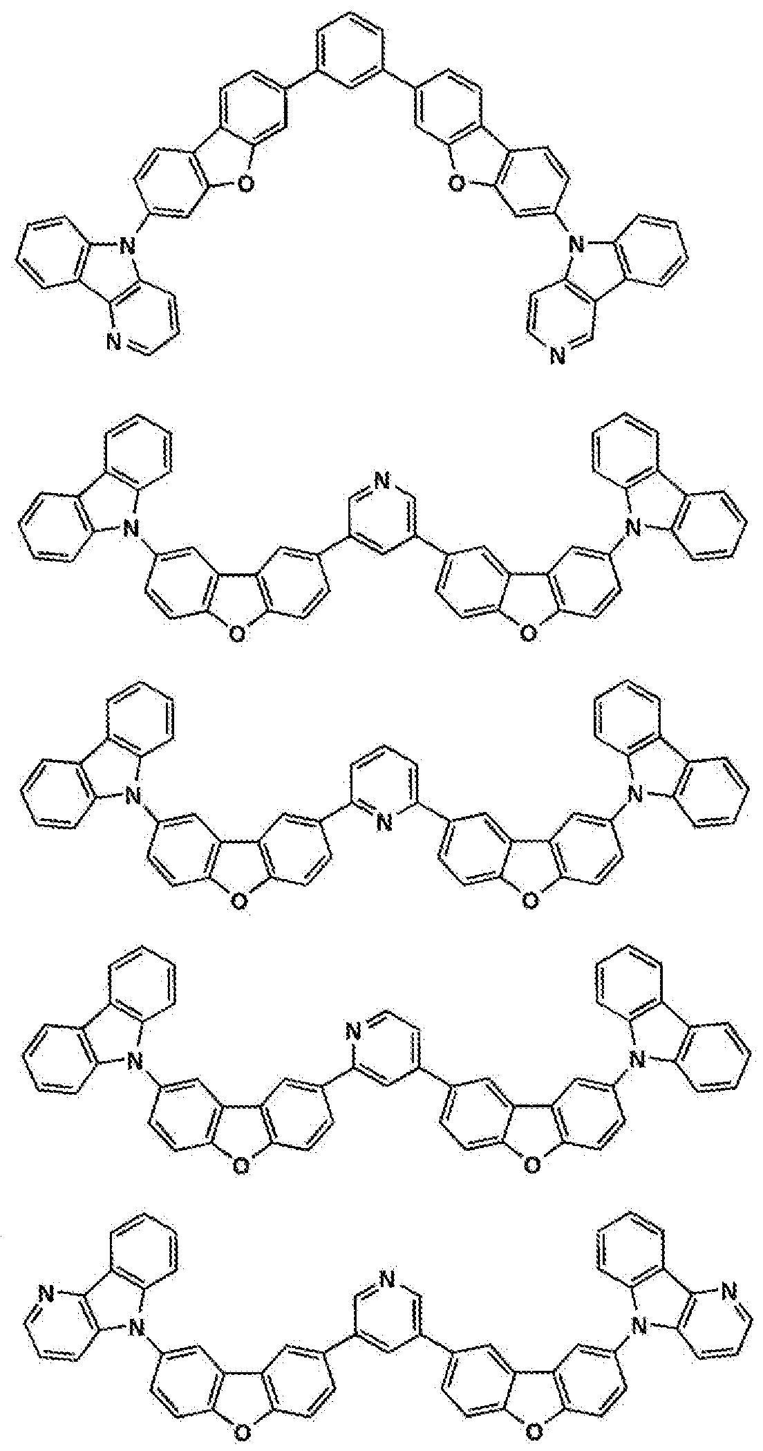
[0073] [化 8]
[0073] [Chemical 8]

[0074] [化 9]
[0074] [Chemical 9]

[0075] [化 10]
[0075] [Chemical 10]

[0076] [化 11]
[0076] [Chemical 11]

[0077] [化 12]
[0077] [Chemical 12]

[0078] [化 13]
[0078] [Chemical 13]

[0079] [化 14]
[0079] [Chemical 14]

[0080] 尚、本発明に係る一般式 (A)で表される化合物の合成は、当該業者周知の合成法 を適用または参照(例えば、後述するホスト化合物において記載の公知文献等)して 合成することが出来る。 [0080] The compound represented by the general formula (A) according to the present invention is synthesized by applying or referring to a synthesis method known to those skilled in the art (for example, a known document described in the host compound described later). I can do it.
[0081] ホスト化合物としては、上記一般式 (A)で表される化合物以外にも、公知のホスト化 合物を単独で用いてもよぐまたは複数種併用して用いてもよい。ホスト化合物を複 数種用いることで、電荷の移動を調整することが可能であり、有機 EL素子を高効率 化すること力 Sできる。また、後述する発光ドーパントを複数種用いることで、異なる発 光を混ぜることが可能となり、これにより任意の発光色を得ることができる。
[0082] また、本発明に用いられる発光ホストとしては、従来公知の低分子化合物でも、繰り 返し単位をもつ高分子化合物でもよぐビュル基やエポキシ基のような重合性基を有 する低分子化合物 (蒸着重合性発光ホスト)でもよレ、。 [0081] As the host compound, in addition to the compound represented by the general formula (A), a known host compound may be used alone or in combination of two or more kinds. By using multiple types of host compounds, it is possible to adjust the movement of electric charges, and it is possible to improve the efficiency of organic EL devices. In addition, by using a plurality of kinds of light emitting dopants described later, it becomes possible to mix different light emission, and thereby any light emission color can be obtained. [0082] The light emitting host used in the present invention may be a conventionally known low molecular compound or a high molecular compound having a repeating unit, and a low molecular compound having a polymerizable group such as a bur group or an epoxy group. It can be a compound (evaporation polymerizable light-emitting host).
[0083] 併用してもよい公知のホスト化合物としては、正孔輸送能、電子輸送能を有しつつ[0083] Known host compounds that may be used in combination may have a hole transport ability and an electron transport ability.
、且つ発光の長波長化を防ぎ、なお且つ高 Tg (ガラス転移温度)である化合物が好 ましい。 Further, a compound that prevents the emission of light from being increased in wavelength and has a high Tg (glass transition temperature) is preferable.
[0084] 公知のホスト化合物の具体例としては、以下の文献に記載されている化合物が挙 げられる。 [0084] Specific examples of known host compounds include compounds described in the following documents.
[0085] 特開 2001— 257076号公報、同 2002— 308855号公報、同 2001— 313179号 公報、同 2002— 319491号公報、同 2001— 357977号公報、同 2002— 334786 号公報、同 2002— 8860号公報、同 2002— 334787号公報、同 2002— 15871号 公報、同 2002— 334788号公報、同 2002— 43056号公報、同 2002— 334789 号公報、同 2002— 75645号公報、同 2002— 338579号公報、同 2002— 10544 5号公報、同 2002— 343568号公報、同 2002— 141173号公報、同 2002— 352 957号公報、同 2002— 203683号公報、同 2002— 363227号公報、同 2002— 2 31453号公報、同 2003— 3165号公報、同 2002— 234888号公報、同 2003— 2 7048号公報、同 2002— 255934号公報、同 2002— 260861号公報、同 2002— 280183号公報、同 2002— 299060号公報、同 2002— 302516号公報、同 2002 — 305083号公報、同 2002— 305084号公報、同 2002— 308837号公報等。 [0085] JP 2001-257076, 2002-308855, 2001-313179, 2002-319491, 2001-357977, 2002-334786, 2002-8860 No., 2002-334787, 2002-15871, 2002-334788, 2002-43056, 2002-334789, 2002-75645, 2002-338579 Gazette, 2002-10544-5, 2002-343568, 2002-141173, 2002-352 957, 2002-203683, 2002-363227, 2002-2 31453, 2003-3165, 2002-234888, 2003-2 7048, 2002-255934, 2002-260861, 2002-280183, 2002- No. 299060, No. 2002-302516, No. 2002-305083, No. 2002-305084, No. 2002-308837, etc.
[0086] (発光ドーパント) [0086] (Luminescent dopant)
本発明に係る発光ドーパントにつ!/、て説明する。 The luminescent dopant according to the present invention will be described below.
[0087] 本発明に係る発光ドーパントとしては、蛍光ドーパント(蛍光性化合物ともレ、う)、リン 光発光性ドーパント (リン光発光体、リン光性化合物、リン光発光性化合物、リン光性 ドーパント等ともいう)を用いることができる力 S、より発光効率の高い有機 EL素子を得 る観点からは、本発明の有機 EL素子の発光層や発光ユニットに使用される発光ドー パント(単に、発光材料ということもある)としては、上記のホスト化合物を含有すると同 時に、リン光発光性ドーパントを含有することが好ましい。 [0087] The light-emitting dopant according to the present invention includes a fluorescent dopant (also a fluorescent compound), a phosphorescent dopant (phosphorescent material, phosphorescent compound, phosphorescent compound, phosphorescent dopant) From the viewpoint of obtaining an organic EL device having higher luminous efficiency S and a higher light emission efficiency, a light emitting dopant (simply emitting light) used in the light emitting layer or light emitting unit of the organic EL device of the present invention is used. As a material), it is preferable to contain a phosphorescent dopant at the same time that the host compound is contained.
[0088] (リン光発光性ドーパント)
本発明に係るリン光発光性ドーパントにつ!、て説明する。 [0088] (phosphorescent dopant) The phosphorescent dopant according to the present invention will be described.
[0089] 本発明に係るリン光発光性ドーパントは、励起三重項からの発光が観測される化合 物であり、具体的には、室温(25°C)にてリン光発光する化合物であり、リン光量子収 率力 S、 25°Cにおいて 0. 01以上の化合物であると定義される力 好ましいリン光量子 収率は 0. 1以上である。 [0089] The phosphorescent dopant according to the present invention is a compound in which light emission from an excited triplet is observed, specifically, a compound that emits phosphorescence at room temperature (25 ° C). Phosphorescence quantum yield power S, a force defined as being a compound of 0.01 or more at 25 ° C. A preferable phosphorescence quantum yield is 0.1 or more.
[0090] 上記リン光量子収率は、第 4版実験化学講座 7の分光 IIの 398頁(1992年版、丸 善)に記載の方法により測定できる。溶液中でのリン光量子収率は種々の溶媒を用 いて測定できるが、本発明に係るリン光発光性ドーパントは、任意の溶媒のいずれか にお!/、て上記リン光量子収率(0. 01以上)が達成されればよ!/、。 [0090] The phosphorescence quantum yield can be measured by the method described in the 4th edition, Experimental Chemistry Course 7, Spectroscopy II, page 398 (1992 edition, Maruzen). The phosphorescence quantum yield in the solution can be measured using various solvents, but the phosphorescent dopant according to the present invention can be used in any solvent! / And the phosphorescence quantum yield (0. 01 or better) is achieved!
[0091] リン光発光性ドーパントの発光は原理としては 2種挙げられ、一つはキャリアが輸送 されるホスト化合物上でキャリアの再結合が起こってホスト化合物の励起状態が生成 し、このエネルギーをリン光発光性ドーパントに移動させることでリン光発光性ドーパ ントからの発光を得るというエネルギー移動型、もう一つはリン光発光性ドーパントが キャリアトラップとなり、リン光発光性ドーパント上でキャリアの再結合が起こりリン光発 光性ドーパントからの発光が得られるというキャリアトラップ型である力 S、いずれの場合 においても、リン光発光性ドーパントの励起状態のエネルギーはホスト化合物の励起 状態のエネルギーよりも低いことが条件である。 [0091] There are two types of light emission of phosphorescent dopants in principle. One is the recombination of carriers on the host compound to which carriers are transported to generate an excited state of the host compound, and this energy is generated. The energy transfer type is to obtain light emission from the phosphorescent dopant by transferring to the phosphorescent dopant, and the other is that the phosphorescent dopant becomes a carrier trap, and the carrier is regenerated on the phosphorescent dopant. In both cases, the excited state energy of the phosphorescent dopant is greater than the excited state energy of the host compound. Low is a condition.
[0092] 《一般式 (B)で表される化合物》 [0092] << Compound Represented by Formula (B) >>
一般式 (B)で表される化合物につ!/、て説明する。 The compound represented by the general formula (B) will be described below.
[0093] 本発明に係るリン光発光性の金属錯体としては、上記一般式 (B)で表される化合 物が好ましく用いられる。 [0093] As the phosphorescent metal complex according to the present invention, a compound represented by the above general formula (B) is preferably used.
[0094] 一般式(B)において、 Rで表される置換基としては、一般式 (A)において、 Al、 A [0094] In the general formula (B), examples of the substituent represented by R include, in the general formula (A), Al, A
1 1
2で各々表される置換基と同義であり、これらの置換基のうち、好ましいものはアルキ ル基もしくはァリール基であり、更に好ましいものは無置換のアルキル基もしくはァリ ール基である。 Each of them is synonymous with the substituent represented by 2, and among these substituents, an alkyl group or an aryl group is preferred, and an unsubstituted alkyl group or an aryl group is more preferred.
[0095] 一般式 (B)において、 Zにより形成される 5〜7員環としては、例えば、ベンゼン環、 ナフタレン環、ピリジン環、ピリミジン環、ピロール環、チォフェン環、ピラゾール環、ィ ミダゾール環、ォキサゾール環及びチアゾール環等が挙げられる。これらのうちで好
ましいものは、ベンゼン環である。 [0095] In the general formula (B), examples of the 5- to 7-membered ring formed by Z include a benzene ring, naphthalene ring, pyridine ring, pyrimidine ring, pyrrole ring, thiophene ring, pyrazole ring, imidazole ring, Examples thereof include an oxazole ring and a thiazole ring. Good out of these The preferred one is the benzene ring.
[0096] 一般式 (B)において、 B〜Bは、各々炭素原子、窒素原子、酸素原子もしくは硫 [0096] In the general formula (B), B to B are each a carbon atom, a nitrogen atom, an oxygen atom or a sulfur atom.
1 5 1 5
黄原子を表し、少なくとも一つは窒素原子であり、該 B 1〜B5より形成される環は、少 なくとも一つの窒素原子を有する芳香族複素環を表す。 Represents a yellow atom, at least one is a nitrogen atom, and the ring formed from B1 to B5 represents an aromatic heterocycle having at least one nitrogen atom.
[0097] 一般式 (B)において、 B〜Bより形成される、少なくとも一つの窒素原子を有する [0097] In the general formula (B), it has at least one nitrogen atom formed from B to B.
1 5 1 5
芳香族複素環としては、例えば、ピロール環、ピラゾール環、イミダゾール環、トリァゾ ール環、テトラゾール環、ォキサゾール環、イソォキサゾール環、チアゾール環、イソ チアゾール環、ォキサジァゾール環及びチアジアゾール環等が挙げられる力 中で も、好ましいものは、ピラゾール環、イミダゾール環であり、特に好ましいのは、イミダゾ ール環である。 Examples of the aromatic heterocycle include pyrrole ring, pyrazole ring, imidazole ring, triazole ring, tetrazole ring, oxazole ring, isoxazole ring, thiazole ring, isothiazole ring, oxaziazole ring and thiadiazole ring. However, a pyrazole ring and an imidazole ring are preferable, and an imidazole ring is particularly preferable.
[0098] これらの環は上記の Rで表される置換基によって更に置換されて!/、てもよ!/、。置換 [0098] These rings may be further substituted with the above-described substituent represented by R! /, Or may be! /. Replace
1 1
基として好ましいものは無置換アルキル基および無置換ァリール基である。 Preferred as the group are an unsubstituted alkyl group and an unsubstituted aryl group.
[0099] 一般式(B)において、 X— L—Xで表される 2座の配位子の具体例としては、例 [0099] In the general formula (B), specific examples of the bidentate ligand represented by X—L—X include
1 1 2 1 1 2
えば、フエ二ルビリジン、フエ二ルビラゾール、フエ二ルイミダゾール、フエニルトリァゾ ール、フエ二ルテトラゾール、ビラザボール、ピコリン酸及びァセチルアセトン等が挙 げられる。また、これらの配位子は上記の Rで表される置換基によって更に置換され For example, phenyl viridine, phenyl virazole, phenyl imidazole, phenyl triazole, phenyl tetrazole, virazabol, picolinic acid and acetylacetone. These ligands are further substituted by the substituent represented by R above.
1 1
ていてもよい。 It may be.
[0100] mlは 1、 2または 3の整数を表し、 m2は 0、 1または 2の整数を表す力 ml + m2は [0100] ml represents an integer of 1, 2 or 3, m2 represents a force of 0, 1 or 2 ml + m2
2または 3である。中でも、 m2は 0である場合が好ましい。 2 or 3. Of these, m2 is preferably 0.
[0101] 一般式 (B)において、 Mで表される金属(金属イオンの場合も含む)としては、元素 [0101] In the general formula (B), the metal represented by M (including the case of metal ions) is an element.
1 1
周期表の 8族〜 10族の遷移金属元素(単に、遷移金属ともいう)が用いられる力 中 でも、イリジウム、白金が好ましぐさらに好ましくはイリジウムである。 Among the forces in which transition metal elements of Group 8 to Group 10 of the periodic table (also simply referred to as transition metals) are used, iridium and platinum are preferred, and iridium is more preferred.
[0102] 尚、一般式 (B)で表されるリン光発光性の金属錯体は、重合性基または反応性基 を有して!/ヽても!/ヽなくてもよ!/、。 [0102] The phosphorescent metal complex represented by the general formula (B) may have a polymerizable group or a reactive group!
[0103] 以下に、一般式 (B)で表されるリン光発光性の金属錯体の具体的な例を挙げるが[0103] Specific examples of the phosphorescent metal complex represented by the general formula (B) are given below.
、本発明はこれらに限定されない。 However, the present invention is not limited to these.
[0104] [化 15]
[0104] [Chemical 15]


[0105] [化 16]
[0105] [Chemical 16]

[0106] [化 17]
[0106] [Chemical 17]

[0107] [化 18]
[0107] [Chemical 18]


[0110] [化 21]
[0110] [Chemical 21]

[0111] [化 22]
[0111] [Chemical 22]

[0112] [化 23]
[0112] [Chemical 23]

[0113] 本発明に係る一般式 (B)で表されるリン光発光性の金属錯体は、例えば、 Inorg. [0113] The phosphorescent metal complex represented by the general formula (B) according to the present invention is, for example, Inorg.
Chem. 40巻、 1704〜1711 ίこ記載の方法等 (こより合成でさる。 Chem. 40, 1704-1711 ί, etc.
[0114] また、本発明では、リン光発光性ドーパントとして、有機 EL素子の発光層に使用さ れる公知のものの中から適宜選択して併用することもできる。 [0114] Further, in the present invention, the phosphorescent dopant can be appropriately selected and used in combination from known ones used for the light emitting layer of the organic EL device.
[0115] 公知のものの中でも、リン光発光性ドーパントとしては、好ましくは元素の周期表で
8〜 10族の金属を含有する錯体系化合物であり、さらに好ましくはイリジウム化合物、 オスミウム化合物、または白金化合物(白金錯体系化合物)、希土類錯体であり、中 でも最も好ましレ、のはイリジウム化合物である。 [0115] Among known ones, the phosphorescent dopant is preferably a periodic table of elements. Complex compounds containing Group 8-10 metals, more preferably iridium compounds, osmium compounds, platinum compounds (platinum complex compounds), rare earth complexes, and most preferred are iridium compounds. It is.
[0116] 以下に、併用してもよい、従来公知のリン光発光性ドーパントとして用いられる化合 物の具体例を示すが、本発明はこれらに限定されない。 [0116] Specific examples of compounds used as conventionally known phosphorescent dopants that may be used in combination are shown below, but the present invention is not limited thereto.
[0117] [化 24] [0117] [Chemical 24]

[0118] [化 25]
[0118] [Chemical 25]


ir— 14
 ir— 14
[0119] [化 26]
[0119] [Chemical 26]

[0120] [化 27]
 [0120] [Chemical 27]
[0121] [化 28]
[0121] [Chemical 28]
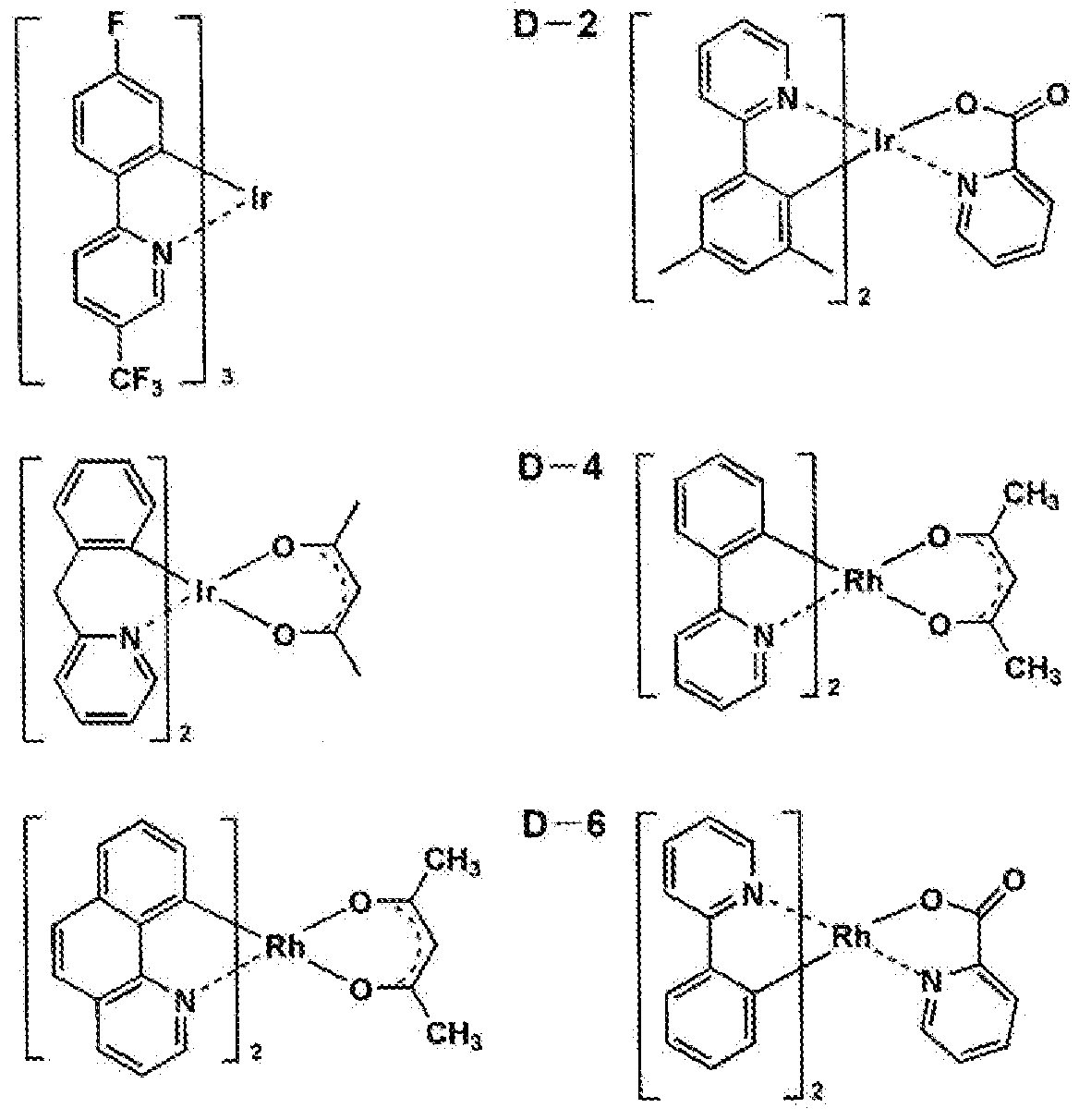
[0122] (蛍光ドーパント (蛍光性化合物とも!/ヽぅ) ) [0122] (Fluorescent dopant (both fluorescent compounds! / ヽ ぅ))
蛍光ドーパントとしては、クマリン系色素、ピラン系色素、シァニン系色素、クロコニ ゥム系色素、スクァリウム系色素、ォキソベンツアントラセン系色素、フルォレセイン系 色素、ローダミン系色素、ピリリウム系色素、ペリレン系色素、スチルベン系色素、ポリ チォフェン系色素、または希土類錯体系蛍光体等が挙げられる。 Fluorescent dopants include coumarin dyes, pyran dyes, cyanine dyes, croconium dyes, squalium dyes, oxobenzanthracene dyes, fluorescein dyes, rhodamine dyes, pyrylium dyes, perylene dyes, Examples thereof include stilbene dyes, polythiophene dyes, and rare earth complex phosphors.
[0123] 次に、本発明の有機 EL素子の構成層として用いられる、注入層、阻止層、電子輸 送層等について説明する。 Next, an injection layer, a blocking layer, an electron transport layer, and the like used as a constituent layer of the organic EL element of the present invention will be described.
[0124] 《注入層:電子注入層、正孔注入層》 [0124] <Injection layer: electron injection layer, hole injection layer>
注入層は必要に応じて設け、電子注入層と正孔注入層があり、上記の如く陽極と 発光層または正孔輸送層の間、及び陰極と発光層または電子輸送層との間に存在 させてもよい。 The injection layer is provided as necessary, and includes an electron injection layer and a hole injection layer, and as described above, exists between the anode and the light emitting layer or hole transport layer and between the cathode and the light emitting layer or electron transport layer. May be.
[0125] 注入層とは、駆動電圧低下や発光輝度向上のために電極と有機層間に設けられる 層のことで、「有機 EL素子とその工業化最前線(1998年 11月 30日ェヌ 'ティー.ェ ス社発行)」の第 2編第 2章「電極材料」(123〜166頁)に詳細に記載されており、正
孔注入層(陽極バッファ一層)と電子注入層(陰極バッファ一層)とがある。 [0125] The injection layer is a layer provided between the electrode and the organic layer in order to reduce the drive voltage and improve the luminance of the light emission. “The organic EL element and the forefront of industrialization (November 30, 1998) 2) Chapter 2 “Electrode Materials” (pages 123-166) There are a hole injection layer (anode buffer layer) and an electron injection layer (a cathode buffer layer).
[0126] 陽極バッファ一層(正孔注入層)は、特開平 9 45479号公報、同 9 260062号 公報、同 8— 288069号公報等にもその詳細が記載されており、具体例として、銅フ タロシアニンに代表されるフタロシアニンバッファ一層、酸化バナジウムに代表される 酸化物バッファ一層、アモルファスカーボンバッファ一層、ポリア二リン(ェメラルディ ン)やポリチォフェン等の導電性高分子を用いた高分子バッファ一層等が挙げられる[0126] Details of the anode buffer layer (hole injection layer) are also described in JP-A-9 45479, JP-A-9 260062, JP-A-8-288069 and the like. Examples include a phthalocyanine buffer layer represented by talocyanine, an oxide buffer layer represented by vanadium oxide, an amorphous carbon buffer layer, and a polymer buffer layer using a conductive polymer such as polyaniline (emeraldine) or polythiophene. Be
〇 Yes
[0127] 陰極バッファ一層(電子注入層)は、特開平 6— 325871号公報、同 9 17574号 公報、同 10— 74586号公報等にもその詳細が記載されており、具体的にはストロン チウムゃアルミニウム等に代表される金属バッファ一層、フッ化リチウムに代表される アルカリ金属化合物バッファ一層、フッ化マグネシウムに代表されるアルカリ土類金 属化合物バッファ一層、酸化アルミニウムに代表される酸化物バッファ一層等が挙げ られる。上記バッファ一層(注入層)はごく薄い膜であることが望ましぐ素材にもよる がその膜厚は 0· 11 111〜5 111の範囲が好ましい。 [0127] The details of the cathode buffer layer (electron injection layer) are also described in JP-A-6-325871, JP-A-9-17574, JP-A-10-74586, and the like. Specifically, strontium Metal buffer layer typified by aluminum, alkali metal compound buffer layer typified by lithium fluoride, alkaline earth metal compound buffer layer typified by magnesium fluoride, oxide buffer layer typified by aluminum oxide Etc. The thickness of the buffer layer (injection layer) is preferably in the range of 0 · 11 111 to 5 111, although it depends on the material desired to be a very thin film.
[0128] 《阻止層:正孔阻止層、電子阻止層》 [0128] <Blocking layer: hole blocking layer, electron blocking layer>
阻止層は、上記の如く有機化合物薄膜の基本構成層の他に必要に応じて設けら れるものである。例えば、特開平 11— 204258号公報、同 11— 204359号公報、及 び「有機 EL素子とその工業化最前線( 1998年 11月 30日ェヌ 'ティー ·エス社発行) 」の 237頁等に記載されている正孔阻止(ホールブロック)層がある。 The blocking layer is provided as necessary in addition to the basic constituent layer of the organic compound thin film as described above. For example, see pages 237 of JP-A-11-204258, JP-A-11-204359, and “OLEDs and the Forefront of Industrialization (issued on November 30, 1998 by TS Co., Ltd.)”. There is a hole blocking layer described.
[0129] 正孔阻止層とは、広い意味では電子輸送層の機能を有し、電子を輸送する機能を 有しつつ正孔を輸送する能力が著しく小さい正孔阻止材料からなり、電子を輸送し つつ正孔を阻止することで電子と正孔の再結合確率を向上させることができる。 [0129] The hole blocking layer has a function of an electron transport layer in a broad sense, and is composed of a hole blocking material having a function of transporting electrons and a very small ability to transport holes, and transports electrons. However, the probability of recombination of electrons and holes can be improved by blocking holes.
[0130] また、後述する電子輸送層の構成を必要に応じて、本発明に係わる正孔阻止層と して用いること力 Sでさる。 [0130] Further, the structure of the electron transport layer, which will be described later, is used as a hole blocking layer according to the present invention, if necessary.
[0131] 本発明の有機 EL素子の正孔阻止層は、発光層に隣接して設けられていることが好 ましい。 [0131] The hole blocking layer of the organic EL device of the present invention is preferably provided adjacent to the light emitting layer.
[0132] 正孔阻止層には、前述のホスト化合物として挙げたァザカルバゾール誘導体を含 有することが好ましい。
[0133] また、本発明にお!/、ては、複数の発光色の異なる複数の発光層を有する場合、そ の発光極大波長が最も短波にある発光層が、全発光層中、最も陽極に近いことが好 ましいが、このような場合、該最短波層と該層の次に陽極に近い発光層との間に正孔 阻止層を追加して設けることが好ましい。更には、該位置に設けられる正孔阻止層に 含有される化合物の 50質量%以上が、前記最短波発光層のホスト化合物に対しそ のイオン化ポテンシャルが 0. 3eV以上大き!/、ことが好まし!/、。 [0132] The hole blocking layer preferably contains the azacarbazole derivative mentioned as the host compound. [0133] Also, in the present invention, when having a plurality of light emitting layers having different light emission colors, the light emitting layer having the shortest wavelength of the light emission maximum is the most anode among all the light emitting layers. In such a case, it is preferable to additionally provide a hole blocking layer between the shortest wave layer and the light emitting layer next to the anode next to the shortest wave layer. Furthermore, it is preferable that 50% by mass or more of the compound contained in the hole blocking layer provided at the position has an ionization potential of 0.3 eV or more with respect to the host compound of the shortest wave emitting layer. Better!/,.
[0134] イオン化ポテンシャルは化合物の HOMO (最高被占分子軌道)レベルにある電子 を真空準位に放出するのに必要なエネルギーで定義され、例えば下記に示すような 方法により求めることができる。 [0134] The ionization potential is defined by the energy required to emit an electron at the HOMO (highest occupied molecular orbital) level of a compound to the vacuum level, and can be obtained by the following method, for example.
[0135] (1)米国 Gaussian社製の分子軌道計算用ソフトウェアである Gaussian98 (Gauss ian98、 Revision A. 丄 1. 4, M. J. Frisch, et ai, Gaussian, Inc. , Pitts ourg h PA, 2002. )を用い、キーワードとして B3LYP/6— 31G *を用いて構造最適 化を行うことにより算出した値 (eV単位換算値)の小数点第 2位を四捨五入した値とし てイオン化ポテンシャルを求めることができる。この計算値が有効な背景には、この手 法で求めた計算直と実験直の相関が高いためである。 [0135] (1) Gaussian98 (Gaussian98, Revision A. 丄 1.4, MJ Frisch, et ai, Gaussian, Inc., Pitts ourgh PA, 2002.) The ionization potential can be obtained by rounding off the second decimal place of the value (eV unit conversion value) calculated by structural optimization using B3LYP / 6-31G * as a keyword. The reason why this calculated value is effective is that there is a high correlation between the calculated value obtained by this method and the experimental value.
[0136] (2)イオン化ポテンシャルは光電子分光法で直接測定する方法により求めることも できる。例えば、理研計器社製の低エネルギー電子分光装置「Model AC— 1」を 用いて、あるいは紫外光電子分光として知られて!/、る方法を好適に用いることができ [0136] (2) The ionization potential can also be obtained by a method of direct measurement by photoelectron spectroscopy. For example, a low energy electron spectrometer “Model AC-1” manufactured by Riken Keiki Co., Ltd. or a method known as ultraviolet photoelectron spectroscopy can be suitably used.
[0137] 一方、電子阻止層とは広い意味では正孔輸送層の機能を有し、正孔を輸送する機 能を有しつつ電子を輸送する能力が著しく小さい材料からなり、正孔を輸送しつつ電 子を阻止することで電子と正孔の再結合確率を向上させることができる。また、後述 する正孔輸送層の構成を必要に応じて電子阻止層として用いることができる。本発明 に係る正孔阻止層、電子輸送層の膜厚としては、好ましくは 3nm〜; !OOnmであり、 更に好ましくは 5nm〜30nmである。 [0137] On the other hand, the electron blocking layer has a function of a hole transport layer in a broad sense, and is made of a material that has a function of transporting holes and has an extremely small ability to transport electrons, and transports holes. However, by blocking electrons, the probability of recombination of electrons and holes can be improved. Moreover, the structure of the positive hole transport layer mentioned later can be used as an electron blocking layer as needed. The film thickness of the hole blocking layer and the electron transporting layer according to the present invention is preferably 3 nm to;! OOnm, and more preferably 5 nm to 30 nm.
[0138] 《正孔輸送層》 [0138] << Hole Transport Layer >>
正孔輸送層とは正孔を輸送する機能を有する正孔輸送材料からなり、広い意味で 正孔注入層、電子阻止層も正孔輸送層に含まれる。正孔輸送層は単層または複数
層設けること力 Sでさる。 The hole transport layer is made of a hole transport material having a function of transporting holes. In a broad sense, a hole injection layer and an electron blocking layer are also included in the hole transport layer. Single or multiple hole transport layers Use layer force S.
[0139] 正孔輸送材料としては、正孔の注入または輸送、電子の障壁性の!/、ずれかを有す るものであり、有機物、無機物のいずれであってもよい。例えば、トリァゾール誘導体 、ォキサジァゾール誘導体、イミダゾール誘導体、ポリアリールアルカン誘導体、ビラ ゾリン誘導体及びピラゾロン誘導体、フエ二レンジァミン誘導体、ァリールァミン誘導 体、ァミノ置換カルコン誘導体、ォキサゾール誘導体、スチリルアントラセン誘導体、 フルォレノン誘導体、ヒドラゾン誘導体、スチルベン誘導体、シラザン誘導体、ァニリ ン系共重合体、また導電性高分子オリゴマー、特にチォフェンオリゴマー等が挙げら れる。 [0139] The hole transport material has either injection or transport of holes, electron barrier properties! /, Or a deviation, and may be either organic or inorganic. For example, triazole derivatives, oxadiazole derivatives, imidazole derivatives, polyarylalkane derivatives, virazoline derivatives and pyrazolone derivatives, phenylenediamine derivatives, arylamine derivatives, amino-substituted chalcone derivatives, oxazole derivatives, styrylanthracene derivatives, fluorenone derivatives, hydrazone derivatives, Examples thereof include stilbene derivatives, silazane derivatives, aniline copolymers, and conductive polymer oligomers, particularly thiophene oligomers.
[0140] 正孔輸送材料としては上記のものを使用することができる力 ポルフィリン化合物、 芳香族第 3級ァミン化合物及びスチリルァミン化合物、特に芳香族第 3級ァミン化合 物を用いることが好ましい。 [0140] The ability to use the above-mentioned materials as the hole transport material [0140] It is preferable to use a porphyrin compound, an aromatic tertiary amine compound and a styrylamine compound, particularly an aromatic tertiary amine compound.
[0141] 芳香族第 3級ァミン化合物及びスチリルアミン化合物の代表例としては、 N, N, N ' , N ーテトラフエニノレー 4, A' ージァミノフエ二ノレ; N, N ージフエニノレー N, N ' —ビス(3—メチルフエ二ル)一〔1 , 1' —ビフエ二ル〕一 4, 4' —ジァミン(TPD) ; 2, 2 ビス(4 ジ一 p トリルァミノフエニル)プロパン; 1 , 1—ビス(4 ジ一 p トリ ノレアミノフエ二ノレ)シクロへキサン; N, N, N' , N' —テトラ一 p トリノレ一 4, A' - ジアミノビフエニル; 1 , 1—ビス(4—ジ一 p トリルァミノフエニル) 4—フエ二ルシク 口へキサン;ビス(4 -ジメチルァミノ一 2 メチルフエ二ノレ)フエニルメタン;ビス(4 -ジ —p トリルァミノフエ二ノレ)フエニルメタン; N, N' —ジフエ二ノレ一 N, N' —ジ(4— メトキシフエ二ル)一 4, 一ジアミノビフエ二ノレ; N, N, N' , N' —テトラフエ二ノレ 4, 4' ージアミノジフエニルエーテル; 4, 4' ビス(ジフエニルァミノ)クオ一ドリフ ェニル; N, N, N—トリ(p—トリル)ァミン; 4—(ジ—p—トリルァミノ)ー 一〔4—(ジ —p—トリルァミノ)スチリル〕スチルベン; 4— N, N ジフエニルアミノー(2 ジフエ二 ノレビニノレ)ベンゼン; 3—メトキシ一 4' — N, N ジフエ二ルアミノスチルベンゼン; N フエ二ルカルバゾール、更には米国特許第 5, 061 , 569号明細書に記載されて いる 2個の縮合芳香族環を分子内に有するもの、例えば、 4, 4' —ビス〔N— ( 1—ナ フチル) N フエニルァミノ〕ビフヱニル(NPD)、特開平 4 308688号公報に記
載されているトリフエニルァミンユニットが 3つスターバースト型に連結された 4, 4' ,[0141] Representative examples of aromatic tertiary amine compounds and styrylamine compounds include N, N, N ', N-tetraphenenole 4, A'-diaminofienol; N, N-diphenenole N, N' — Bis (3-methylphenyl) -1- [1, 1'-biphenyl] -1,4,4'-diamine (TPD); 2,2 Bis (4-di-triphenylaminophenyl) propane; Bis (4 di-l-tri-noraminophenyl) cyclohexane; N, N, N ', N' —tetra-l-trinore 4, A'-diaminobiphenyl; 1, 1-bis (4-di-l p Triphenylamino) 4-hexane phenyl hexane; bis (4-dimethylamino-2-methylphenyl) phenylmethane; bis (4-di-p-trimethylaminophenyl) phenylmethane; N, N '— diphenyleno N , N '—Di (4-methoxyphenyl) -1,4 diaminobiphenol; N, N, N', N'—tetraphenyl 4,4′-diaminodiphenyl ether; 4,4 ′ bis (diphenylamino) quadophenyl; N, N, N-tri (p-tolyl) amine; 4- (di-p— Trirylamino)-1 [4- (di-p-tolylamino) styryl] stilbene; 4-N, N diphenylamino- (2 diphenylenobininole) benzene; 3-methoxy-1 4 '— N, N diphenylaminostil Benzene; N phenylcarbazole, as well as those having two fused aromatic rings in the molecule as described in US Pat. No. 5,061,569, for example, 4, 4′-bis [N — (1-Naphthyl) N phenylamino] biphenyl (NPD), described in JP-A-4 308688 Three triphenylamine units are connected in a starburst type 4, 4 ',
A" —トリス〔N— (3—メチルフエニル) N フエニルァミノ〕トリフエニルァミン(MTDA "-tris [N- (3-methylphenyl) N phenylamino] triphenylamine (MTD
ATA)等が挙げられる。 ATA) and the like.
[0142] 更にこれらの材料を高分子鎖に導入した、またはこれらの材料を高分子の主鎖とし た高分子材料を用いることもできる。また、 p型 Si、 p型 SiC等の無機化合物も正 孔注入材料、正孔輸送材料として使用することができる。 [0142] Furthermore, a polymer material in which these materials are introduced into a polymer chain or these materials as a polymer main chain can also be used. Inorganic compounds such as p-type Si and p-type SiC can also be used as the hole injecting material and hole transporting material.
[0143] また、特開平 1 1— 251067号公報、 J. Huang et. al.著文献 (Applied Physic s Letters 80 (2002) , ρ· 139)に記載されているような、所謂 p型正孔輸送材料 を用いることもできる。本発明においては、より高効率の発光素子が得られることから これらの材料を用いることが好まし!/、。 [0143] Also, the so-called p-type hole described in JP-A-11-251067, J. Huang et. Al. (Applied Physics Letters 80 (2002), ρ · 139). Transport materials can also be used. In the present invention, it is preferable to use these materials because a light emitting element with higher efficiency can be obtained!
[0144] 正孔輸送層は上記正孔輸送材料を、例えば、真空蒸着法、スピンコート法、キャス ト法、インクジェット法を含む印刷法、 LB法等の公知の方法により、薄膜化することに より形成すること力でさる。 [0144] The hole transport layer is formed by thinning the hole transport material by a known method such as a vacuum deposition method, a spin coating method, a casting method, a printing method including an ink jet method, or an LB method. It takes more power to form.
[0145] 正孔輸送層の膜厚については特に制限はないが、通常は 51 111〜5 111程度、好ま しくは 5nm〜200nmである。この正孔輸送層は上記材料の 1種または 2種以上から なる一層構造であってもよレ、。 [0145] The thickness of the hole transport layer is not particularly limited, but is usually about 51111 to 5111, preferably 5 nm to 200 nm. The hole transport layer may have a single layer structure composed of one or more of the above materials.
[0146] また、不純物をドープした p性の高い正孔輸送層を用いることもできる。その例とし ては、特開平 4— 297076号公報、特開 2000— 196140号公報、同 2001— 1021[0146] In addition, a hole transport layer having a high p property doped with impurities may be used. Examples thereof include JP-A-4-297076, JP-A-2000-196140, 2001-1021.
75号公報の各公報、 J. Appl. Phys . , 95, 5773 (2004)等に記載されたものが挙 げられる。 The publications in each publication of the Gazette No. 75, J. Appl. Phys., 95, 5773 (2004), and the like.
[0147] 本発明においては、このような ρ性の高い正孔輸送層を用いることが、より低消費電 力の素子を作製することができるため好ましい。 [0147] In the present invention, it is preferable to use such a hole transport layer having a high ρ property because a device with lower power consumption can be produced.
[0148] 《電子輸送層》 [0148] 《Electron Transport Layer》
電子輸送層とは電子を輸送する機能を有する材料からなり、広い意味で電子注入 層、正孔阻止層も電子輸送層に含まれる。電子輸送層は単層または複数層設けるこ と力 Sできる。 The electron transport layer is made of a material having a function of transporting electrons, and in a broad sense, an electron injection layer and a hole blocking layer are also included in the electron transport layer. The electron transport layer can be provided with a single layer or multiple layers.
[0149] 従来、単層の電子輸送層、及び複数層とする場合は発光層に対して陰極側に隣 接する電子輸送層に用いられる電子輸送材料 (正孔阻止材料を兼ねる)としては、陰
極より注入された電子を発光層に伝達する機能を有していればよぐその材料として は従来公知の化合物の中力 任意のものを選択して用いることができる。 Conventionally, in the case of a single electron transport layer and a plurality of layers, as an electron transport material (also serving as a hole blocking material) used for an electron transport layer adjacent to the light emitting layer on the cathode side, Any material having a function of transmitting electrons injected from the electrode to the light emitting layer may be selected and used as a material of any conventionally known compound.
[0150] 例えば、ニトロ置換フルオレン誘導体、ジフヱ二ルキノン誘導体、チォピランジオキ シド誘導体、カルポジイミド、フレオレニリデンメタン誘導体、アントラキノジメタン及び アントロン誘導体、ォキサジァゾール誘導体等が挙げられる。 [0150] Examples include nitro-substituted fluorene derivatives, diphenylquinone derivatives, thiopyrandioxide derivatives, carpositimide, fluorenylidenemethane derivatives, anthraquinodimethane and anthrone derivatives, oxadiazole derivatives, and the like.
[0151] 更に、上記ォキサジァゾール誘導体において、ォキサジァゾール環の酸素原子を 硫黄原子に置換したチアジアゾール誘導体、電子吸引基として知られているキノキ サリン環を有するキノキサリン誘導体も、電子輸送材料として用いることができる。 [0151] Further, in the above oxadiazole derivative, a thiadiazole derivative in which the oxygen atom of the oxaziazole ring is substituted with a sulfur atom, or a quinoxaline derivative having a quinoxaline ring known as an electron-withdrawing group can also be used as an electron transport material.
[0152] 更にこれらの材料を高分子鎖に導入した、またはこれらの材料を高分子の主鎖とし た高分子材料を用いることもできる。 [0152] Further, a polymer material in which these materials are introduced into a polymer chain or these materials are used as a polymer main chain can also be used.
[0153] また、 8 キノリノール誘導体の金属錯体、例えば、トリス(8 キノリノール)アルミ二 ゥム(Alq)、トリス(5, 7—ジクロロ一 8—キノリノール)アルミニウム、トリス(5, 7—ジブ 口モー 8 キノリノール)ァノレミニゥム、トリス(2 メチノレー 8 -キノリノール)アルミユウ ム、トリス(5—メチル 8—キノリノール)アルミニウム、ビス(8—キノリノール)亜鉛(Zn q)等、及びこれらの金属錯体の中心金属が In、 Mg、 Cu、 Ca、 Sn、 Gaまたは Pbに 置き替わった金属錯体も、電子輸送材料として用いることができる。 [0153] In addition, metal complexes of 8 quinolinol derivatives such as tris (8 quinolinol) aluminum (Alq), tris (5,7-dichloro-1-8-quinolinol) aluminum, tris (5,7-dib mouth mode) The central metal of these metal complexes is 8 quinolinol) anoreminium, tris (2 methinolay 8 -quinolinol) aluminum, tris (5-methyl 8-quinolinol) aluminum, bis (8-quinolinol) zinc (Zn q), etc. Metal complexes replacing Mg, Cu, Ca, Sn, Ga or Pb can also be used as electron transport materials.
[0154] その他、メタルフリーもしくはメタルフタロシアニン、またはそれらの末端がアルキル 基ゃスルホン酸基等で置換されているものも、電子輸送材料として好ましく用いること 力 Sできる。また、発光層の材料として例示したジスチリルビラジン誘導体も、電子輸送 材料として用いること力 Sできるし、正孔注入層、正孔輸送層と同様に n型 Si、 n型 SiC等の無機半導体も電子輸送材料として用いることができる。 [0154] In addition, metal-free or metal phthalocyanine, or those having a terminal substituted with an alkyl group or a sulfonic acid group can be preferably used as an electron transporting material. In addition, the distyrylvirazine derivative exemplified as the material for the light-emitting layer can also be used as an electron transport material, and, like the hole injection layer and the hole transport layer, inorganic semiconductors such as n-type Si and n-type SiC Can also be used as an electron transporting material.
[0155] 電子輸送層は上記電子輸送材料を、例えば、真空蒸着法、スピンコート法、キャス ト法、インクジェット法を含む印刷法、 LB法等の公知の方法により、薄膜化することに より形成すること力でさる。 [0155] The electron transport layer is formed by thinning the electron transport material by a known method such as, for example, a vacuum deposition method, a spin coating method, a casting method, a printing method including an inkjet method, or an LB method. It ’s the power to do.
[0156] 電子輸送層の膜厚については特に制限はないが、通常は 51 111〜5 111程度、好ま しくは 5nm〜200nmである。電子輸送層は上記材料の 1種または 2種以上からなる 一層構造であってもよい。 [0156] The thickness of the electron transport layer is not particularly limited, but is usually about 51 111 to 5 111, preferably 5 to 200 nm. The electron transport layer may have a single layer structure composed of one or more of the above materials.
[0157] また、不純物をドープした n性の高い電子輸送層を用いることもできる。その例とし
ては、特開平 4— 297076号公報、同 10— 270172号公報、特開 2000— 196140 号公報、同 2001— 102175号公報、 J. Appl. Phys. , 95, 5773 (2004)等に記載 されたものが挙げられる。 [0157] In addition, an electron transport layer having a high n property doped with impurities can be used. As an example Are described in JP-A-4-297076, JP-A-10-270172, JP-A-2000-196140, 2001-102175, J. Appl. Phys., 95, 5773 (2004), etc. Can be mentioned.
[0158] 本発明においては、このような η性の高い電子輸送層を用いることがより低消費電 力の素子を作製することができるため好ましい。 In the present invention, it is preferable to use such an electron transport layer having a high η property because a device with lower power consumption can be produced.
[0159] 《陽極》 [0159] 《Anode》
有機 EL素子における陽極としては、仕事関数の大きい (4eV以上)金属、合金、電 気伝導性化合物及びこれらの混合物を電極物質とするものが好ましく用いられる。こ のような電極物質の具体例としては、 Au等の金属、 Cul、インジウムチンォキシド(IT 0)、 SnO、 ZnO等の導電性透明材料が挙げられる。また、 IDIXO (In O— ZnO) 等非晶質で透明導電膜を作製可能な材料を用いてもよい。 As the anode in the organic EL device, an electrode material made of a metal, an alloy, an electrically conductive compound or a mixture thereof having a high work function (4 eV or more) is preferably used. Specific examples of such electrode materials include metals such as Au, and conductive transparent materials such as Cul, indium tin oxide (IT 0), SnO, and ZnO. Alternatively, an amorphous material such as IDIXO (In 2 O—ZnO) that can produce a transparent conductive film may be used.
[0160] 陽極はこれらの電極物質を蒸着やスパッタリング等の方法により薄膜を形成させ、 フォトリソグラフィ一法で所望の形状のパターンを形成してもよぐあるいはパターン精 度をあまり必要としな!/、場合は(100 μ m以上程度)、上記電極物質の蒸着やスパッ タリング時に所望の形状のマスクを介してパターンを形成してもよい。 [0160] The anode may be formed by depositing these electrode materials by a method such as vapor deposition or sputtering, and a pattern of a desired shape may be formed by a single photolithography method, or pattern accuracy is not required! / In this case (in the case of about 100 μm or more), a pattern may be formed through a mask having a desired shape during the deposition or sputtering of the electrode material.
[0161] あるいは、有機導電性化合物のように塗布可能な物質を用いる場合には、印刷方 式、コーティング方式等湿式成膜法を用いることもできる。 [0161] Alternatively, when a material that can be applied, such as an organic conductive compound, is used, a wet film formation method such as a printing method or a coating method can also be used.
[0162] この陽極より発光を取り出す場合には、透過率を 10%より大きくすることが望ましぐ また、陽極としてのシート抵抗は数百 Ω /口以下が好ましい。更に膜厚は材料にもよ る力 通常、 10nm〜; !OOOnmの範囲、好ましくは 10nm〜200nmの範囲で選ばれ [0162] In the case of taking out light emission from this anode, it is desirable that the transmittance be greater than 10%. Further, the sheet resistance as the anode is preferably several hundred Ω / mouth or less. Furthermore, the thickness depends on the material. Usually, it is selected in the range of 10 nm to OOOnm, preferably in the range of 10 nm to 200 nm.
[0163] 《陰極》 [0163] 《Cathode》
一方、陰極としては仕事関数の小さレ、(4eV以下)金属(電子注入性金属と称する) 、合金、電気伝導性化合物及びこれらの混合物を電極物質とするものが用いられる。 このような電極物質の具体例としては、ナトリウム、ナトリウム—カリウム合金、マグネシ ゥム、リチウム、マグネシウム/銅混合物、マグネシウム/銀混合物、マグネシウム/ アルミニウム混合物、マグネシウム/インジウム混合物、アルミニウム/酸化アルミ二 ゥム (Al O )混合物、インジウム、リチウム/アルミニウム混合物、希土類金属等が挙
げられる。 On the other hand, a cathode having a small work function, (4 eV or less) metal (referred to as an electron injecting metal), alloy, electrically conductive compound, and a mixture thereof is used as an electrode material. Specific examples of such electrode materials include sodium, sodium-potassium alloy, magnesium, lithium, magnesium / copper mixture, magnesium / silver mixture, magnesium / aluminum mixture, magnesium / indium mixture, aluminum / aluminum oxide. (Al 2 O 3) mixture, indium, lithium / aluminum mixture, rare earth metal, etc. I can get lost.
[0164] これらの中で、電子注入性及び酸化等に対する耐久性の点から、電子注入性金属 とこれより仕事関数の値が大きく安定な金属である第二金属との混合物、例えば、マ グネシゥム/銀混合物、マグネシウム/アルミニウム混合物、マグネシウム/インジゥ ム混合物、アルミニウム/酸化アルミニウム (Al O )混合物、リチウム/アルミニウム Among these, from the viewpoint of electron injection property and durability against oxidation, etc., a mixture of an electron injection metal and a second metal which is a stable metal having a larger work function value than this, for example, magnesium. / Silver mixture, magnesium / aluminum mixture, magnesium / indium mixture, aluminum / aluminum oxide (Al 2 O) mixture, lithium / aluminum
2 3 twenty three
混合物、アルミニウム等が好適である。陰極はこれらの電極物質を蒸着やスパッタリ ング等の方法により薄膜を形成させることにより、作製すること力 sできる。 Mixtures, aluminum and the like are preferred. The cathode can be produced by forming a thin film of these electrode materials by a method such as vapor deposition or sputtering.
[0165] また、陰極としてのシート抵抗は数百 Ω /口以下が好ましぐ膜厚は通常 10nm〜 [0165] The sheet resistance as the cathode is preferably several hundred Ω / mouth or less.
5〃 m、好ましくは 50nm〜200nmの範囲で選ばれる。 It is selected in the range of 5 μm, preferably 50 nm to 200 nm.
[0166] 尚、発光した光を透過させるため、有機 EL素子の陽極または陰極のいずれか一方 が透明または半透明であれば発光輝度が向上し好都合である。 [0166] In order to transmit the emitted light, if either one of the anode or the cathode of the organic EL element is transparent or translucent, the emission luminance is advantageously improved.
[0167] また、陰極に上記金属を lnm〜20nmの膜厚で作製した後に、陽極の説明で挙げ た導電性透明材料をその上に作製することで、透明または半透明の陰極を作製する ことができ、これを応用することで陽極と陰極の両方が透過性を有する素子を作製す ること力 Sでさる。 [0167] In addition, after forming the above metal on the cathode with a film thickness of lnm to 20nm, a transparent transparent or translucent cathode is manufactured by forming the conductive transparent material mentioned in the description of the anode thereon. By applying this, it is possible to produce a device in which both the anode and the cathode are transparent.
[0168] 《支持基板》 [0168] 《Support substrate》
本発明の有機 EL素子に用いることのできる支持基板(以下、基体、基板、基材、支 持体等とも言う)としては、ガラス、プラスチック等の種類には特に限定はなぐまた透 明であっても不透明であってもよい。 As a support substrate (hereinafter also referred to as a substrate, substrate, substrate, support, etc.) that can be used in the organic EL device of the present invention, there is no particular limitation on the type of glass, plastic, etc., and it is transparent. Or opaque.
[0169] 支持基板側から光を取り出す場合には、支持基板は透明であることが好ましい。好 ましく用いられる透明な支持基板としては、ガラス、石英、透明樹脂フィルムを挙げる こと力 Sできる。特に好ましい支持基板は、有機 EL素子にフレキシブル性を与えること が可能な樹脂フィルムである。 [0169] When light is extracted from the support substrate side, the support substrate is preferably transparent. Examples of the transparent support substrate that is preferably used include glass, quartz, and a transparent resin film. A particularly preferable support substrate is a resin film capable of giving flexibility to the organic EL element.
[0170] 樹脂フィルムとしては、例えば、ポリエチレンテレフタレート(PET)、ポリエチレンナ フタレート(PEN)等のポリエステル、ポリエチレン、ポリプロピレン、セロファン、セル口 ースジアセテート、セルローストリアセテート、セルロースアセテートブチレート、セル口 ースアセテートプロピオネート(CAP)、セルロースアセテートフタレート(TAC)、セル ロースナイトレート等のセルロースエステル類またはそれらの誘導体、ポリ塩化ビニリ
デン、ポリビニノレアノレコーノレ、ポリエチレンビニノレアノレコーノレ、シンジオタクティックポ リスチレン、ポリカーボネート、ノルボルネン樹脂、ポリメチルペンテン、ポリエーテルケ トン、ポリイミド、ポリエーテルスルホン(PES)、ポリフエ二レンスルフイド、ポリスルホン 類、ポリエーテルイミド、ポリエーテルケトンイミド、ポリアミド、フッ素樹脂、ナイロン、ポ リメチルメタタリレート、アクリルあるいはポリアリレート類、アートン(商品名 JSR社製) あるいはァペル (商品名三井化学社製)とレ、つたシクロォレフイン系樹脂等を挙げら れる。 [0170] Examples of the resin film include polyesters such as polyethylene terephthalate (PET) and polyethylene naphthalate (PEN), polyethylene, polypropylene, cellophane, cellulose diacetate, cellulose triacetate, cellulose acetate butyrate, cellulose acetoacetate pro. Cellulose esters such as pionate (CAP), cellulose acetate phthalate (TAC), cellulose nitrate, or their derivatives, polyvinyl chloride Denene, Polyvinylenorenoreconole, Polyethylene Vinylenorenoreconole, Syndiotactic Polystyrene, Polycarbonate, Norbornene Resin, Polymethylpentene, Polyether Ketone, Polyimide, Polyethersulfone (PES), Polyphenylenesulfide, Polysulfones, Polyetherimide, polyetherketoneimide, polyamide, fluororesin, nylon, polymethylmethacrylate, acrylic or polyarylates, Arton (trade name, made by JSR) or Vapelle (trade name, made by Mitsui Chemicals), And cycloolefin-based resins.
[0171] 樹脂フィルムの表面には、無機物、有機物の被膜またはその両者のハイブリッド被 膜が形成されていてもよぐ JIS K 7129— 1992に準拠した方法で測定された、水 蒸気透過度(25 ± 0. 5°C、相対湿度(90 ± 2) %RH)が 0. Olg/ (m2' 24h)以下の ノ リア性フィルムであることが好ましぐ更には、 JIS K 7126— 1987に準拠した方 法で測定された酸素透過度が、 1 X 10— 3ml/ (m2* 24h*MPa)以下、水蒸気透過度 ヽ 10— 5g/ (m2- 24h)以下の高バリア性フィルムであることが好まし!/、。 [0171] On the surface of the resin film, an inorganic film, an organic film, or a hybrid film of the both may be formed. Water vapor permeability measured by a method in accordance with JIS K 7129-1992 (25 It is preferable that the film is a non-reactive film with ± 0.5 ° C and relative humidity (90 ± 2)% RH) of 0. Olg / (m 2 '24h) or less. Further, in JIS K 7126-1987 oxygen permeability measured in compliant way is, 1 X 10- 3 ml / ( m 2 * 24h * MPa) or less, the water vapor transmission rateヽ 10- 5 g / (m 2 - 24h) or less of a high barrier property I prefer it to be a film!
[0172] ノ リア膜を形成する材料としては、水分や酸素等素子の劣化をもたらすものの浸入 を抑制する機能を有する材料であればよぐ例えば、酸化珪素、二酸化珪素、窒化 珪素等を用いることができる。更に該膜の脆弱性を改良するために、これら無機層と 有機材料からなる層の積層構造を持たせることがより好ましい。無機層と有機層の積 層順につ!/、ては特に制限はな!/、が、両者を交互に複数回積層させることが好まし!/ヽ [0172] As the material for forming the noria film, any material may be used as long as it has a function of suppressing the intrusion of the elements such as moisture and oxygen. For example, silicon oxide, silicon dioxide, silicon nitride, or the like is used. Can do. Further, in order to improve the brittleness of the film, it is more preferable to have a laminated structure of these inorganic layers and organic material layers. The inorganic layer and the organic layer are stacked in order! /, But there are no particular restrictions! /, But it is preferable to stack both layers alternately! / ヽ
[0173] ノ リア膜の形成方法については特に限定はなぐ例えば、真空蒸着法、スパッタリ ング法、反応性スパッタリング法、分子線エピタキシー法、クラスターイオンビーム法、 イオンプレーティング法、プラズマ重合法、大気圧プラズマ重合法、プラズマ CVD法 、レーザー CVD法、熱 CVD法、コーティング法等を用いることができる力 特開 200 4— 68143号公報に記載されているような大気圧プラズマ重合法によるものが特に 好ましい。 [0173] The formation method of the noria film is not particularly limited, for example, vacuum deposition method, sputtering method, reactive sputtering method, molecular beam epitaxy method, cluster ion beam method, ion plating method, plasma polymerization method, large size Force capable of using atmospheric pressure plasma polymerization method, plasma CVD method, laser CVD method, thermal CVD method, coating method, etc. Especially those using atmospheric pressure plasma polymerization method as described in JP-A-2004-68143 preferable.
[0174] 不透明な支持基板としては、例えば、アルミ、ステンレス等の金属板、フィルムゃ不 透明樹脂基板、セラミック製の基板等が挙げられる。 [0174] Examples of the opaque support substrate include a metal plate such as aluminum and stainless steel, a film or an opaque resin substrate, a ceramic substrate, and the like.
[0175] 本発明の有機 EL素子の発光の室温における外部取り出し効率は、 1 %以上である
こと力 S好ましく、より好ましくは 5%以上である。 [0175] The external extraction efficiency at room temperature of light emission of the organic EL device of the present invention is 1% or more Power S is preferable, and more preferably 5% or more.
[0176] ここで、外部取り出し量子効率(%) =有機 EL素子外部に発光した光子数/有機 E[0176] Here, external extraction quantum efficiency (%) = number of photons emitted outside the organic EL element / organic E
L素子に流した電子数 X 100である。 The number of electrons flowing through the L element is X 100.
[0177] また、カラーフィルタ一等の色相改良フィルタ一等を併用しても、有機 EL素子から の発光色を蛍光体を用いて多色へ変換する色変換フィルターを併用してもよい。色 変換フィルターを用いる場合においては、有機 EL素子の発光の maxは 480nm以 下が好ましい。 [0177] In addition, a hue improvement filter such as a color filter may be used in combination, or a color conversion filter that converts light emitted from an organic EL element into multiple colors using a phosphor may be used in combination. When a color conversion filter is used, the maximum light emission of the organic EL element is preferably 480 nm or less.
[0178] 《封止》 [0178] <Sealing>
本発明に用いられる封止手段としては、例えば、封止部材と電極、支持基板とを接 着剤で接着する方法を挙げることができる。 Examples of the sealing means used in the present invention include a method of bonding a sealing member, an electrode, and a support substrate with an adhesive.
[0179] 封止部材としては、有機 EL素子の表示領域を覆うように配置されておればよぐ凹 板状でも平板状でもよい。また透明性、電気絶縁性は特に問わない。 [0179] The sealing member may be a concave plate shape or a flat plate shape as long as it is arranged so as to cover the display region of the organic EL element. Further, transparency and electrical insulation are not particularly limited.
[0180] 具体的には、ガラス板、ポリマー板'フィルム、金属板'フィルム等が挙げられる。ガ ラス板としては、特にソーダ石灰ガラス、ノ リウム 'ストロンチウム含有ガラス、鉛ガラス[0180] Specific examples include a glass plate, a polymer plate 'film, a metal plate' film and the like. Glass plates include soda-lime glass, norlium-strontium-containing glass, and lead glass.
、アルミノケィ酸ガラス、ホウケィ酸ガラス、ノ リウムホウケィ酸ガラス、石英等を挙げる こと力 Sでさる。 Examples include aluminosilicate glass, borosilicate glass, borosilicate glass, and quartz.
[0181] また、ポリマー板としては、ポリカーボネート、アタリノレ、ポリエチレンテレフタレート、 ポリエーテルサルファイド、ポリサルフォン等を挙げることができる。金属板としては、 ステンレス、鉄、銅、アルミニウム、マグネシウム、ニッケル、亜鉛、クロム、チタン、モリ ブテン、シリコン、ゲルマニウム及びタンタルからなる群から選ばれる一種以上の金属 または合金からなるものが挙げられる。 [0181] Examples of the polymer plate include polycarbonate, attalinole, polyethylene terephthalate, polyether sulfide, and polysulfone. Examples of the metal plate include those made of one or more metals or alloys selected from the group consisting of stainless steel, iron, copper, aluminum, magnesium, nickel, zinc, chromium, titanium, molybdenum, silicon, germanium, and tantalum.
[0182] 本発明においては、素子を薄膜化できるということからポリマーフィルム、金属フィル ムを好ましく使用することができる。更には、ポリマーフィルムは、 JIS K 7126 - 19 87に準拠した方法で測定された酸素透過度が、 1 X 10—31111/ (1112'
 以下 、 JIS K 7129— 1992に準拠した方法で測定された、水蒸気透過度(25 ± 0. 5°C 、相対湿度(90土 2) %RH)が 10— 5g/ (m2- 24h)以下のものであることが好まし!/、。 [0182] In the present invention, a polymer film and a metal film can be preferably used because the element can be thinned. Furthermore, the polymer film, JIS K 7126 - 19 oxygen permeability measured in compliance with the method provided in 87, 1 X 10- 3 1111 / ( 111 2 ' Hereinafter, it was measured by the method based on JIS K 7129- 1992, water vapor transmission rate (25 ± 0. 5 ° C, relative humidity (90 Sat 2)% RH) is 10- 5 g / (m 2 - 24h) The following are preferred!
[0183] 封止部材を凹状に加工するのは、サンドブラスト加工、化学エッチング加工等が使 われる。接着剤として具体的には、アクリル酸系オリゴマー、メタクリル酸系オリゴマー
の反応性ビュル基を有する光硬化及び熱硬化型接着剤、 2—シァノアクリル酸エス テル等の湿気硬化型等の接着剤を挙げることができる。 [0183] The sealing member is processed into a concave shape by sandblasting, chemical etching, or the like. Specific examples of adhesives include acrylic acid oligomers and methacrylic acid oligomers. And photo-curing and thermosetting adhesives having a reactive bur group, and moisture-curing adhesives such as 2-cyanacrylate ester.
[0184] また、エポキシ系等の熱及び化学硬化型(二液混合)を挙げること力 Sできる。また、 ホットメルト型のポリアミド、ポリエステル、ポリオレフインを挙げること力 Sできる。また、力 チオン硬化タイプの紫外線硬化型エポキシ樹脂接着剤を挙げることができる。 [0184] In addition, mention may be made of an epoxy-based heat- and chemical-curing type (two-component mixing). In addition, hot-melt polyamides, polyesters and polyolefins can be listed. Moreover, a force thione curable type ultraviolet curable epoxy resin adhesive can be mentioned.
[0185] 尚、有機 EL素子が熱処理により劣化する場合があるので、室温から 80°Cまでに接 着硬化できるものが好ましい。また、前記接着剤中に乾燥剤を分散させておいてもよ い。封止部分への接着剤の塗布は市販のディスペンサーを使ってもよいし、スクリー ン印刷のように印刷してもよレ、。 [0185] In addition, since the organic EL element may be deteriorated by heat treatment, it is preferable that the adhesive can be cured from room temperature to 80 ° C. A desiccant may be dispersed in the adhesive. A commercially available dispenser may be used to apply the adhesive to the sealing part, or it may be printed like screen printing.
[0186] また、有機層を挟み支持基板と対向する側の電極の外側に該電極と有機層を被覆 し、支持基板と接する形で無機物、有機物の層を形成し封止膜とすることも好適にで きる。この場合、該膜を形成する材料としては、水分や酸素等素子の劣化をもたらす ものの浸入を抑制する機能を有する材料であればよぐ例えば、酸化珪素、二酸化 珪素、窒化珪素等を用いることができる。 [0186] Alternatively, the electrode and the organic layer may be coated on the outer side of the electrode facing the support substrate with the organic layer interposed therebetween, and an inorganic or organic layer may be formed in contact with the support substrate to form a sealing film. It can be preferred. In this case, as a material for forming the film, any material may be used as long as it has a function of suppressing intrusion of elements that cause deterioration of elements such as moisture and oxygen. For example, silicon oxide, silicon dioxide, silicon nitride, or the like may be used. it can.
[0187] 更に該膜の脆弱性を改良するために、これら無機層と有機材料からなる層の積層 構造を持たせることが好ましい。これらの膜の形成方法については、特に限定はなく 、例えば真空蒸着法、スパッタリング法、反応性スパッタリング法、分子線ェピタキシ 一法、クラスターイオンビーム法、イオンプレーティング法、プラズマ重合法、大気圧 プラズマ重合法、プラズマ CVD法、レーザー CVD法、熱 CVD法、コーティング法等 を用いること力 Sでさる。 [0187] Further, in order to improve the brittleness of the film, it is preferable to have a laminated structure of these inorganic layers and layers made of an organic material. The method for forming these films is not particularly limited. For example, vacuum deposition, sputtering, reactive sputtering, molecular beam epitaxy, cluster ion beam, ion plating, plasma polymerization, atmospheric pressure plasma Use the polymerization method, plasma CVD method, laser CVD method, thermal CVD method, coating method, etc.
[0188] 封止部材と有機 EL素子の表示領域との間隙には、気相及び液相では、窒素、ァ ルゴン等の不活性気体やフッ化炭化水素、シリコンオイルのような不活性液体を注入 すること力 S好ましい。また真空とすることも可能である。また、内部に吸湿性化合物を 封人することあでさる。 [0188] In the gap between the sealing member and the display area of the organic EL element, an inert gas such as nitrogen or argon, or an inert liquid such as fluorinated hydrocarbon or silicon oil is used in the gas phase or liquid phase. Injecting power S is preferred. A vacuum is also possible. It is also possible to seal hygroscopic compounds inside.
[0189] 吸湿性化合物としては、例えば、金属酸化物(例えば、酸化ナトリウム、酸化カリウム 、酸化カルシウム、酸化バリウム、酸化マグネシウム、酸化アルミニウム等)、硫酸塩( 例えば、硫酸ナトリウム、硫酸カルシウム、硫酸マグネシウム、硫酸コバルト等)、金属 ハロゲン化物(例えば、塩化カルシウム、塩化マグネシウム、フッ化セシウム、フッ化タ
ンタル、臭化セリウム、臭化マグネシウム、沃化バリウム、沃化マグネシウム等)、過塩 素酸類 (例えば、過塩素酸バリウム、過塩素酸マグネシウム等)等が挙げられ、硫酸 塩、金属ハロゲン化物及び過塩素酸類においては無水塩が好適に用いられる。 [0189] Examples of the hygroscopic compound include metal oxides (for example, sodium oxide, potassium oxide, calcium oxide, barium oxide, magnesium oxide, aluminum oxide), sulfates (for example, sodium sulfate, calcium sulfate, magnesium sulfate). , Cobalt sulfate, etc.), metal halides (eg, calcium chloride, magnesium chloride, cesium fluoride, titanium fluoride) Tantalum, cerium bromide, magnesium bromide, barium iodide, magnesium iodide, etc.), perchloric acids (eg, barium perchlorate, magnesium perchlorate, etc.), sulfates, metal halides and the like In perchloric acids, anhydrous salts are preferably used.
[0190] 《保護膜、保護板》 [0190] 《Protective film, protective plate》
有機層を挟み支持基板と対向する側の前記封止膜、あるいは前記封止用フィルム の外側に、素子の機械的強度を高めるために保護膜、あるいは保護板を設けてもよ い。特に封止が前記封止膜により行われている場合には、その機械的強度は必ずし も高くないため、このような保護膜、保護板を設けることが好ましい。これに使用するこ と力 Sできる材料としては、前記封止に用いたのと同様なガラス板、ポリマー板'フィル ム、金属板'フィルム等を用いることができる力 軽量且つ薄膜化ということからポリマ 一フィルムを用いることが好ましレ、。 In order to increase the mechanical strength of the element, a protective film or a protective plate may be provided outside the sealing film or the sealing film on the side facing the support substrate with the organic layer interposed therebetween. In particular, when the sealing is performed by the sealing film, the mechanical strength is not necessarily high. Therefore, it is preferable to provide such a protective film and a protective plate. The force that can be used for this S The material that can be used is the same glass plate, polymer plate 'film, metal plate' film, etc. used for the sealing. It is preferable to use a polymer film.
[0191] 《光取り出し》 [0191] 《Light extraction》
有機 EL素子は空気よりも屈折率の高い(屈折率が 1. 7〜2. 1程度)層の内部で発 光し、発光層で発生した光のうち 15%から 20%程度の光しか取り出せないことがー 般的に言われている。 The organic EL element emits light inside a layer with a higher refractive index than air (refractive index of about 1.7 to 2.1), and only 15% to 20% of the light generated in the light emitting layer can be extracted. It is generally said that there is nothing.
[0192] これは、臨界角以上の角度 Θで界面(透明基板と空気との界面)に入射する光は、 全反射を起こし素子外部に取り出すことができないことや、透明電極ないし発光層と 透明基板との間で光が全反射を起こし、光が透明電極ないし発光層を導波し、結果 として光が素子側面方向に逃げるためである。 [0192] This is because light incident on the interface (interface between the transparent substrate and air) at an angle Θ greater than the critical angle causes total reflection and cannot be extracted outside the device. This is because light undergoes total reflection with the substrate, and the light is guided through the transparent electrode or the light emitting layer, and as a result, the light escapes in the side direction of the element.
[0193] この光の取り出しの効率を向上させる手法としては、例えば、透明基板表面に凹凸 を形成し、透明基板と空気界面での全反射を防ぐ方法 (米国特許第 4, 774, 435号 明細書)、基板に集光性を持たせることにより効率を向上させる方法(特開昭 63— 31 4795号公報)、素子の側面等に反射面を形成する方法(特開平 1— 220394号公 報)、基板と発光体の間に中間の屈折率を持つ平坦層を導入し、反射防止膜を形成 する方法 (特開昭 62— 172691号公報)、基板と発光体の間に基板よりも低屈折率 を持つ平坦層を導入する方法(特開 2001— 202827号公報)、基板、透明電極層 や発光層のいずれかの層間 (含む、基板と外界間)に回折格子を形成する方法 (特 開平 11— 283751号公報)等がある。
[0194] 本発明においては、これらの方法を本発明の有機 EL素子と組み合わせて用いるこ とができるが、基板と発光体の間に基板よりも低屈折率を持つ平坦層を導入する方 法、あるいは基板、透明電極層や発光層のいずれかの層間(含む、基板と外界間) に回折格子を形成する方法を好適に用いることができる。 [0193] As a technique for improving the light extraction efficiency, for example, a method of forming irregularities on the surface of the transparent substrate to prevent total reflection at the interface between the transparent substrate and the air (US Pat. No. 4,774,435) ), A method of improving the efficiency by giving the light condensing property to the substrate (Japanese Patent Laid-Open No. 63-314795), a method of forming a reflective surface on the side surface of the element (Japanese Patent Laid-Open No. 1-2220394) ), A method of forming an antireflection film by introducing a flat layer having an intermediate refractive index between the substrate and the light emitter (Japanese Patent Laid-Open No. 62-172691), and lower than the substrate between the substrate and the light emitter. A method of introducing a flat layer having a refractive index (Japanese Patent Laid-Open No. 2001-202827), and a method of forming a diffraction grating between the substrate, the transparent electrode layer and the light emitting layer (including between the substrate and the outside world) (Kaihei 11-283751). [0194] In the present invention, these methods can be used in combination with the organic EL device of the present invention, but a method of introducing a flat layer having a lower refractive index than the substrate between the substrate and the light emitter. Alternatively, a method of forming a diffraction grating between any one of the substrate, the transparent electrode layer, and the light emitting layer (including between the substrate and the outside) can be suitably used.
[0195] 本発明はこれらの手段を組み合わせることにより、更に高輝度あるいは耐久性に優 れた素子を得ることができる。 [0195] By combining these means, the present invention can provide a device having higher brightness or durability.
[0196] 透明電極と透明基板の間に低屈折率の媒質を光の波長よりも長い厚みで形成する と、透明電極から出てきた光は、媒質の屈折率が低いほど外部への取り出し効率が 高くなる。 [0196] When a medium with a low refractive index is formed between the transparent electrode and the transparent substrate with a thickness longer than the wavelength of the light, the light extracted from the transparent electrode is extracted to the outside as the refractive index of the medium decreases. Becomes higher.
[0197] 低屈折率層としては、例えば、エア口ゲル、多孔質シリカ、フッ化マグネシウム、フッ 素系ポリマー等が挙げられる。透明基板の屈折率は一般に 1. 5〜; 1. 7程度であるの で、低屈折率層は屈折率がおよそ 1. 5以下であることが好ましい。また、更に 1. 35 以下であることが好ましい。 [0197] Examples of the low refractive index layer include air-mouth gel, porous silica, magnesium fluoride, fluorine-based polymer, and the like. Since the refractive index of the transparent substrate is generally about 1.5 to about 1.7, the low refractive index layer preferably has a refractive index of about 1.5 or less. Further, it is preferably 1.35 or less.
[0198] また、低屈折率媒質の厚みは媒質中の波長の 2倍以上となるのが望ましい。これは 低屈折率媒質の厚みが、光の波長程度になってエバネッセントで染み出した電磁波 が基板内に入り込む膜厚になると、低屈折率層の効果が薄れるからである。 [0198] The thickness of the low refractive index medium is preferably at least twice the wavelength in the medium. This is because the effect of the low refractive index layer is diminished when the thickness of the low refractive index medium is about the wavelength of light and the electromagnetic wave exuded by evanescent enters the substrate.
[0199] 全反射を起こす界面もしくはいずれかの媒質中に回折格子を導入する方法は、光 取り出し効率の向上効果が高レ、とレ、う特徴がある。 [0199] The method of introducing a diffraction grating into an interface or any medium that causes total reflection has a feature that the effect of improving the light extraction efficiency is high.
[0200] この方法は回折格子が 1次の回折や 2次の回折といった所謂ブラッグ回折により、 光の向きを屈折とは異なる特定の向きに変えることができる性質を利用して、発光層 力も発生した光のうち層間での全反射等により外に出ることができない光を、いずれ かの層間もしくは、媒質中(透明基板内や透明電極内)に回折格子を導入することで 光を回折させ、光を外に取り出そうとするものである。 [0200] This method uses the property that the diffraction grating can change the direction of light to a specific direction different from refraction by so-called Bragg diffraction, such as first-order diffraction and second-order diffraction. The light that cannot be emitted outside due to total internal reflection between layers is diffracted by introducing a diffraction grating into any layer or medium (inside a transparent substrate or transparent electrode) It tries to take out light.
[0201] 導入する回折格子は、二次元的な周期屈折率を持って!/、ること力 S望まし!/、。これは 発光層で発光する光はあらゆる方向にランダムに発生するので、ある方向にのみ周 期的な屈折率分布を持っている一般的な 1次元回折格子では、特定の方向に進む 光しか回折されず、光の取り出し効率がさほど上がらない。 [0201] The diffraction grating to be introduced has a two-dimensional periodic refractive index! This is because light emitted from the light-emitting layer is randomly generated in all directions, so a general one-dimensional diffraction grating having a periodic refractive index distribution only in one direction diffracts only light traveling in a specific direction. The light extraction efficiency does not increase so much.
[0202] しかしながら、屈折率分布を二次元的な分布にすることにより、あらゆる方向に進む
光が回折され、光の取り出し効率が上がる。 [0202] However, by making the refractive index distribution a two-dimensional distribution, it proceeds in all directions. The light is diffracted and the light extraction efficiency is increased.
[0203] 回折格子を導入する位置としては前述の通り、いずれかの層間もしくは媒質中(透 明基板内や透明電極内)でもよいが、光が発生する場所である有機発光層の近傍が 望ましい。 [0203] As described above, the position where the diffraction grating is introduced may be in any one of the layers or in the medium (in the transparent substrate or the transparent electrode), but is preferably in the vicinity of the organic light emitting layer where light is generated. .
[0204] このとき、回折格子の周期は媒質中の光の波長の約 1/2〜3倍程度が好ましい。 [0204] At this time, the period of the diffraction grating is preferably about 1/2 to 3 times the wavelength of light in the medium.
[0205] 回折格子の配列は正方形のラチス状、三角形のラチス状、ハニカムラチス状等、 2 次元的に配列が繰り返されることが好ましい。 [0205] The arrangement of the diffraction grating is preferably two-dimensionally repeated, such as a square lattice, a triangular lattice, or a honeycomb lattice.
[0206] 《集光シート》 [0206] [Condenser sheet]
本発明の有機 EL素子は基板の光取り出し側に、例えば、マイクロレンズアレイ状の 構造を設けるように加工したり、あるいは所謂集光シートと組み合わせることにより、特 定方向、例えば、素子発光面に対し正面方向に集光することにより、特定方向上の 輝度を高めることができる。 The organic EL device of the present invention can be processed on a light extraction side of a substrate, for example, by providing a microlens array-like structure, or combined with a so-called condensing sheet, in a specific direction, for example, on the device light emitting surface. On the other hand, by focusing light in the front direction, the brightness in a specific direction can be increased.
[0207] マイクロレンズアレイの例としては、基板の光取り出し側に一辺が 30〃 mでその頂 角が 90度となるような四角錐を 2次元に配列する。一辺は 10 m〜; 100 mが好ま しい。これより小さくなると回折の効果が発生して色付ぐ大きすぎると厚みが厚くなり 好ましくない。 [0207] As an example of a microlens array, a quadrangular pyramid with a side of 30 mm and an apex angle of 90 degrees is arranged two-dimensionally on the light extraction side of the substrate. One side is 10m ~; 100m is preferred. If it is smaller than this, the effect of diffraction is generated, and if the color is too large, the thickness becomes thick, which is not preferable.
[0208] 集光シートとしては、例えば、液晶表示装置の LEDバックライトで実用化されている ものを用いることが可能である。このようなシートとして、例えば、住友スリーェム社製 輝度上昇フィルム(BEF)等を用いることができる。プリズムシートの形状としては、例 えば、基材に頂角 90度、ピッチ 50〃 mの△状のストライプが形成されたものであって もよいし、頂角が丸みを帯びた形状、ピッチをランダムに変化させた形状、その他の 形状であってもよい。 [0208] As the condensing sheet, for example, a sheet that has been put to practical use in an LED backlight of a liquid crystal display device can be used. As such a sheet, for example, a brightness enhancement film (BEF) manufactured by Sumitomo 3EM may be used. As the shape of the prism sheet, for example, the base material may be formed by forming a △ -shaped stripe with a vertex angle of 90 degrees and a pitch of 50 mm, or a shape with a rounded vertex angle and a pitch. The shape may be changed randomly or other shapes.
[0209] また、発光素子からの光放射角を制御するために、光拡散板'フィルムを集光シー トと併用してもよい。例えば、(株)きもと製拡散フィルム (ライトアップ)等を用いること ができる。 [0209] Further, in order to control the light emission angle from the light emitting element, a light diffusing plate 'film may be used in combination with the condensing sheet. For example, a diffusion film (light-up) manufactured by Kimoto Co., Ltd. can be used.
[0210] 《有機 EL素子の作製方法》 [0210] <Method for manufacturing organic EL element>
本発明の有機 EL素子の作製方法の一例として、陽極/正孔注入層/正孔輸送層 /発光層/電子輸送層/電子注入層/陰極からなる有機 EL素子の作製法を説明
する。 As an example of the method for producing the organic EL device of the present invention, a method for producing an organic EL device comprising an anode / hole injection layer / hole transport layer / light emitting layer / electron transport layer / electron injection layer / cathode is described. To do.
[0211] まず適当な基体上に所望の電極物質、例えば、陽極用物質力 なる薄膜を 1 m 以下、好ましくは 10nm〜200nmの膜厚になるように、蒸着やスパッタリング等の方 法により形成させ陽極を作製する。 [0211] First, a desired electrode material, for example, a thin film having a material force for an anode, is formed on a suitable substrate by a method such as vapor deposition or sputtering so as to have a thickness of 1 m or less, preferably 10 nm to 200 nm. An anode is produced.
[0212] 次に、この上に有機 EL素子材料である正孔注入層、正孔輸送層、発光層、正孔阻 止層、電子輸送層、電子注入層等の有機化合物薄膜を形成させる。 Next, organic compound thin films such as a hole injection layer, a hole transport layer, a light emitting layer, a hole blocking layer, an electron transport layer, and an electron injection layer, which are organic EL element materials, are formed thereon.
[0213] これら各層の形成方法としては、前記の如く蒸着法、ウエットプロセス (スピンコート 法、キャスト法、インクジェット法、印刷法)等がある力、均質な膜が得られやすぐ且 つピンホールが生成しにくい等の点から、本発明においてはスピンコート法、インクジ エツト法、印刷法等の塗布法による成膜が好ましぐ特にインクジェット法が好ましい。 [0213] As a method for forming each of these layers, as described above, a vapor deposition method, a wet process (spin coating method, casting method, ink jet method, printing method), etc. can be used, and a homogeneous film can be obtained immediately. In the present invention, film formation by a coating method such as a spin coating method, an ink jet method, and a printing method is preferable, and an inkjet method is particularly preferable.
[0214] 本発明においては、発光層の形成において、本発明に係る有機金属錯体を溶解ま たは分散した液を用いて塗布法により成膜することが好ましぐ特に塗布法がインクジ エツト法であることが好ましレ、。 [0214] In the present invention, in the formation of the light emitting layer, it is preferable to form a film by a coating method using a solution in which the organometallic complex according to the present invention is dissolved or dispersed. In particular, the coating method is an ink jet method. It is preferred to be.
[0215] 本発明に係る有機金属錯体を溶解または分散する液媒体としては、例えば、メチル ェチルケトン、シクロへキサノン等のケトン類、酢酸ェチル等の脂肪酸エステル類、ジ クロ口ベンゼン等のハロゲン化炭化水素類、 DMF、 DMSO等の有機溶媒を用いるこ と力 Sできる。 [0215] Examples of the liquid medium for dissolving or dispersing the organometallic complex according to the present invention include, for example, ketones such as methyl ethyl ketone and cyclohexanone, fatty acid esters such as ethyl acetate, and halogenated carbonization such as dichlorobenzene. It is possible to use organic solvents such as hydrogen, DMF, and DMSO.
[0216] また分散方法としては、超音波、高剪断力分散やメディア分散等の分散方法により 分散すること力でさる。 [0216] Further, as a dispersion method, the dispersion is performed by a dispersion method such as ultrasonic wave, high shearing force dispersion or media dispersion.
[0217] これらの層を形成後、その上に陰極用物質からなる薄膜を 1 μ m以下、好ましくは、 50nm〜200nmの範囲の膜厚になるように、例えば、蒸着やスパッタリング等の方法 により形成させ、陰極を設けることにより所望の有機 EL素子が得られる。 [0217] After these layers are formed, a thin film made of a cathode material is formed thereon with a thickness of 1 μm or less, preferably 50 nm to 200 nm, for example, by a method such as vapor deposition or sputtering. By forming the cathode and providing the cathode, a desired organic EL device can be obtained.
[0218] また作製順序を逆にして、陰極、電子注入層、電子輸送層、発光層、正孔輸送層、 正孔注入層、陽極の順に作製することも可能である。このようにして得られた多色の 表示装置に、直流電圧を印加する場合には陽極を +、陰極を一の極性として電圧 2 V〜40V程度を印加すると発光が観測できる。また交流電圧を印加してもよい。なお 、印加する交流の波形は任意でよい。 [0218] Further, the production order can be reversed, and the cathode, electron injection layer, electron transport layer, light emitting layer, hole transport layer, hole injection layer, and anode can be produced in this order. When a DC voltage is applied to the multicolor display device thus obtained, light emission can be observed by applying a voltage of about 2 V to 40 V with the anode as + and the cathode as one polarity. An alternating voltage may be applied. The alternating current waveform to be applied may be arbitrary.
[0219] 《用途》
本発明の有機 EL素子は、表示デバイス、ディスプレイ、各種発光光源として用いる ことができる。発光光源として、例えば、照明装置 (家庭用照明、車内照明)、時計や 液晶用バックライト、看板広告、信号機、光記憶媒体の光源、電子写真複写機の光 源、光通信処理機の光源、光センサーの光源等が挙げられるがこれらに限定されな い。 [0219] 《Use》 The organic EL element of the present invention can be used as a display device, a display, and various light sources. Examples of light sources include lighting devices (home lighting, interior lighting), clock and liquid crystal backlights, billboard advertisements, traffic lights, light sources of optical storage media, light sources of electrophotographic copying machines, light sources of optical communication processors, Examples include, but are not limited to, light sources of optical sensors.
[0220] 用途しては、特に液晶表示装置のバックライト、照明用光源として有効に用いること ができる。 [0220] In particular, it can be effectively used as a backlight of a liquid crystal display device and a light source for illumination.
[0221] 本発明の有機 EL素子においては、必要に応じ成膜時にメタルマスクやインクジエツ トプリンティング法等でパターユングを施してもよい。パターユングする場合は、電極 のみをパターユングしてもよいし、電極と発光層をパターユングしてもよいし、素子全 層をパターユングしてもよぐ素子の作製においては、従来公知の方法を用いること ができる。 [0221] In the organic EL device of the present invention, patterning may be performed by a metal mask, an ink jet printing method, or the like as needed during film formation. In the case of patterning, only the electrode may be patterned, the electrode and the light emitting layer may be patterned, or in the production of an element that may be patterned on the entire layer, a conventionally known method Method can be used.
[0222] 本発明の有機 EL素子や本発明に係る化合物の発光する色は、「新編色彩科学ハ ンドブック」(日本色彩学会編、東京大学出版会、 1985)の 108頁の図 4. 16におい て、分光放射輝度計 CS - 1000 (コニ力ミノルタセンシング社製)で測定した結果を C IE色度座標に当てはめたときの色で決定される。 [0222] The light emission color of the organic EL device of the present invention and the compound of the present invention is shown in Fig. 4.16 on page 108 of "New Color Science Handbook" (Edited by the Japan Society for Color Science, University of Tokyo Press, 1985). The color measured when the result of measurement with the spectral radiance meter CS-1000 (manufactured by Koni Force Minolta Sensing) is applied to the CIE chromaticity coordinates.
[0223] また、本発明の有機 EL素子が白色素子の場合には、白色とは、 2度視野角正面輝 度を上記方法により測定した際に、 1000Cd/m2での CIE1931表色系における色 度力 Χ=0. 33 ± 0. 07、Υ = 0. 33 ± 0. 07の領域内にあることを言う。 [0223] Further, when the organic EL device of the present invention is a white device, white means that in the CIE1931 color system at 1000 Cd / m 2 when the 2 ° viewing angle front luminance is measured by the above method. Chromatic force is in the region of Χ = 0.33 ± 0.07, Υ = 0.33 ± 0.07.
実施例 Example
[0224] 以下、実施例により本発明を説明するが、本発明はこれらに限定されない。また、 実施例に用レ、る化合物を下記に示す。 [0224] Hereinafter, the present invention will be described by way of examples, but the present invention is not limited thereto. The compounds used in the examples are shown below.
[0225] [化 29]
 [0225] [Chemical 29]
[0226] 実施例 1 [0226] Example 1
《有機 EL素子 1 1の作製》 << Production of organic EL elements 1 1 >>
陽極として lOOmmX lOOmm X l . 1mmのガラス基板上に ITO (インジウムチンォ キシド)を lOOnm成膜した基板(NHテクノグラス社製 NA45)にパターユングを行つ た後、この ITO透明電極を設けた透明支持基板をイソプロピルアルコールで超音波 洗浄し、乾燥窒素ガスで乾燥し、 UVオゾン洗浄を 5分間行った。 The ITO transparent electrode was formed after patterning was performed on a substrate (NH techno glass NA45) in which ITO (indium oxide) was deposited on a lOOmmX lOOmm X l. 1 mm glass substrate as an anode. The transparent support substrate was ultrasonically cleaned with isopropyl alcohol, dried with dry nitrogen gas, and subjected to UV ozone cleaning for 5 minutes.
[0227] この透明支持基板を市販の真空蒸着装置の基板ホルダーに固定し、一方、モリブ デン製抵抗加熱ボートに α NPDを 200mg入れ、別のモリブデン製抵抗加熱ボー トにホスト化合物として CBP200mg入れ、別のモリブデン製抵抗加熱ボートに BCP を 200mg入れ、別のモリブデン製抵抗加熱ボートに例示化合物 1 1を lOOmg入れ 、さらに別のモリブデン製抵抗加熱ボートに Alqを 200mg入れ、真空蒸着装置に取 付けた。 [0227] This transparent support substrate was fixed to a substrate holder of a commercially available vacuum deposition apparatus. Meanwhile, 200 mg of αNPD was placed in a molybden resistance heating boat, and 200 mg of CBP as a host compound was placed in another resistance heating boat made of molybdenum. 200 mg of BCP was put in another molybdenum resistance heating boat, lOOmg of Exemplified Compound 11 was put in another resistance heating boat made of molybdenum, and 200 mg of Alq was put in another resistance heating boat made of molybdenum, and attached to the vacuum evaporation system. .
[0228] 次いで、真空槽を 4 X 10— 4Paまで減圧した後、 α— NPDの入った前記加熱ボート に通電して加熱し、蒸着速度 0. Inm/秒で透明支持基板に蒸着し、膜厚 40nmの 正孔輸送層を設けた。 [0228] Next, after pressure in the vacuum tank was reduced to 4 X 10- 4 Pa, and heated by supplying an electric current to the boat containing alpha-NPD, was deposited on the transparent supporting substrate at a deposition rate of 0. Inm / sec, A hole transport layer with a thickness of 40 nm was provided.
[0229] さらに、 CBPと例示化合物 1 1の入った前記加熱ボートに通電して加熱し、それ ぞれ蒸着速度 0. 2nm/秒、 0. 012nm/秒で前記正孔輸送層上に共蒸着して、膜
厚 40nmの発光層を設けた。なお、蒸着時の基板温度は室温であった。 [0229] Further, the heating boat containing CBP and Exemplified Compound 11 1 was energized and heated, and co-evaporated on the hole transport layer at a deposition rate of 0.2 nm / second and 0.012 nm / second, respectively. And the membrane A light emitting layer having a thickness of 40 nm was provided. In addition, the substrate temperature at the time of vapor deposition was room temperature.
[0230] さらに、 BCPの入った前記加熱ボートに通電して加熱し、蒸着速度 0. lnm/秒で 前記発光層の上に蒸着して膜厚 lOnmの正孔阻止層を設けた。 [0230] Further, the heating boat containing BCP was energized and heated, and was deposited on the light emitting layer at a deposition rate of 0.1 nm / sec to provide a hole blocking layer having a thickness of lOnm.
[0231] その上に、さらに、 Alqの入った前記加熱ボートに通電して加熱し、蒸着速度 0. 1 nm/秒で前記正孔阻止層の上に蒸着してさらに膜厚 40nmの電子輸送層を設けた[0231] Furthermore, the heating boat containing Alq was further energized and heated, and then deposited on the hole blocking layer at a deposition rate of 0.1 nm / second to further transport an electron having a thickness of 40 nm. Layered
。なお、蒸着時の基板温度は室温であった。 . In addition, the substrate temperature at the time of vapor deposition was room temperature.
[0232] 引き続きフッ化リチウム 0. 5nm及びアルミニウム l lOnmを蒸着して陰極を形成し、 有機 EL素子 1 1を作製した。 Subsequently, lithium fluoride 0.5 nm and aluminum lOnm were vapor-deposited to form a cathode, and an organic EL device 11 was produced.
[0233] 《有機 EL素子 1一 2〜;!一 15の作製》 [0233] << Organic EL device 1 1 2 ~ ;! 1 15 preparation >>
有機 EL素子 1 1の作製において、発光層のホスト化合物である CBPを表 1に示 す化合物に置き換え、例示化合物 1 1を表 1に示す化合物に置き換えた以外は同 様にして、有機 EL素子 1— 2〜1— 15を作製した。 In the production of the organic EL device 11, the organic EL device was similarly prepared except that CBP, which is the host compound of the light emitting layer, was replaced with the compound shown in Table 1, and the example compound 11 was replaced with the compound shown in Table 1. 1-2-1-15 were produced.
[0234] 《有機 EL素子 1一 ;!〜 1 15の評価》 [0234] << Evaluation of organic EL element 1;; ~ 1 15 >>
作製した有機 EL素子 1一 1〜;!一 15の評価を行い、その結果を表 1に示す。 The fabricated organic EL devices 1 1 to 1 !! 1 15 were evaluated and the results are shown in Table 1.
[0235] 《有機 EL素子の評価》 [0235] << Evaluation of organic EL elements >>
得られた有機 EL素子 1— 1〜1— 16を評価するに際しては、作製後の各有機 EL 素子の非発光面をガラスケースで覆い、厚み 300 mのガラス基板を封止用基板と して用いて、周囲にシール材としてエポキシ系光硬化型接着剤(東亞合成社製ラック ストラック LC0629B)を適用し、これを上記陰極上に重ねて前記透明支持基板と密 着させ、ガラス基板側から UV光を照射して、硬化させて、封止して、図 3、図 4に示 すような照明装置を形成して評価した。 When evaluating the obtained organic EL devices 1-1 to 1-16, the non-light emitting surface of each organic EL device after fabrication was covered with a glass case, and a glass substrate having a thickness of 300 m was used as a sealing substrate. Using an epoxy-based photo-curing adhesive (Lux Track LC0629B manufactured by Toagosei Co., Ltd.) as a sealing material around it, and overlaying it on the cathode to adhere to the transparent support substrate, and from the glass substrate side It was irradiated with UV light, cured, sealed, and an illumination device as shown in Figs. 3 and 4 was formed and evaluated.
[0236] 図 3は照明装置の概略図を示し、有機 EL素子 101はガラスカバー 102で覆われて いる(なお、ガラスカバーでの封止作業は、有機 EL素子 101を大気に接触させること なく窒素雰囲気下のグローブボックス(純度 99. 999%以上の高純度窒素ガスの雰 囲気下)で行った)。 [0236] FIG. 3 shows a schematic diagram of the lighting device, and the organic EL element 101 is covered with a glass cover 102 (in addition, the sealing operation with the glass cover is performed without bringing the organic EL element 101 into contact with the atmosphere. Glove box in a nitrogen atmosphere (performed in an atmosphere of high-purity nitrogen gas with a purity of 99.999% or higher).
[0237] 図 4は照明装置の断面図を示し、図 4において、 105は陰極、 106は有機 EL層、 1 07は透明電極付きガラス基板を示す。なお、ガラスカバー 102内には窒素ガス 108 が充填され、捕水剤 109が設けられている。
[0238] 《外部取り出し量子効率》 FIG. 4 is a cross-sectional view of the lighting device. In FIG. 4, 105 indicates a cathode, 106 indicates an organic EL layer, and 107 indicates a glass substrate with a transparent electrode. The glass cover 102 is filled with nitrogen gas 108 and a water catching agent 109 is provided. [0238] 《External quantum efficiency》
作製した有機 EL素子について、 23°C、乾燥窒素ガス雰囲気下で 2. 5mA/cm2 定電流を印加した時の外部取り出し量子効率(%)を測定した。なお測定には分光放 射輝度計 CS - 1000 (コニ力ミノルタ製)を用いた。 With respect to the produced organic EL device, the external extraction quantum efficiency (%) was measured when a constant current of 2.5 mA / cm 2 was applied in a dry nitrogen gas atmosphere at 23 ° C. For the measurement, a spectral radiation luminance meter CS-1000 (manufactured by Konica Minolta) was used.
[0239] 表 1の外部取り出し量子効率は、有機 EL素子 1 15の外部取り出し量子効率を 1[0239] The external extraction quantum efficiencies in Table 1 are the same as the external extraction quantum efficiencies of organic EL elements 1 15
00とした時の相対値で表した。 Expressed as a relative value when 00.
[0240] 《寿命》 [0240] <Lifetime>
2. 5mA/cm2の一定電流で駆動したときに、輝度が発光開始直後の輝度(初期 輝度)の半分に低下するのに要した時間を測定し、これを半減寿命時間( τ 0. 5)と して寿命の指標とした。なお測定には分光放射輝度計 CS— 1000 (コニカミノルタ製 )を用いた。尚、表 1の寿命は、有機 EL素子 1—1の寿命を 100とした時の相対値で 表した。得られた結果を表 1に示す。 2. When driving at a constant current of 5 mA / cm 2 , measure the time required for the luminance to drop to half of the luminance immediately after the start of light emission (initial luminance), and calculate this as the half-life time (τ 0.5 ) As an indicator of life. A spectral radiance meter CS-1000 (manufactured by Konica Minolta) was used for the measurement. The life shown in Table 1 is expressed as a relative value when the life of the organic EL element 1-1 is taken as 100. The results obtained are shown in Table 1.
[0241] [表 1]
[0241] [Table 1]
有機 EL素子 No. ド一バント化合物木スト化合物外部取り出し量子効率寿命備 考 Organic EL device No. Dante compound compound Tree strike compound external extraction quantum efficiency lifetime Remarks
1 ― 1 一 1 C8P 100 100比铰例 ί― 2 1 -75 CBP 5 130比棚: 1 ― 1 1 1 C8P 100 100 Comparison example ί― 2 1 -75 CBP 5 130 Ratio shelf:
1 —3 1 -77 CBP 90 20 1 -3 1 -77 CBP 90 20
1 -4 ? - 1 1 130 160本発明14 ? -1 1 130 160 This invention
1 ― 5 卜 1 22 132 155本発明1 ― 5 卜 1 22 132 155 Present invention
1 -6 1 - 1 29 ί28 150本発明1 -6 1-1 29 ί28 150 The present invention
1一 7 1 ― 1 38 2:6 !53本発 ¾1 1 7 1 ― 1 38 2: 6! 53 departures ¾
Ϊ —8 1一 1 41 127 ISO本発明Ϊ —8 1 1 1 41 127 ISO invention
1 - 9 1 ~75 \ !45 250本発明1-9 1 ~ 75 \! 45 250
1 -10 1 -75 6 1 0 230本発明1 -10 1 -75 6 1 0 230 The present invention
1 -11 1 -7S 1? 142 228本発明1 -11 1 -7S 1? 142 228
] -12 1 —75 22 14t 230本発明] -12 1 -75 22 14t 230
1 -13 1 —75. 25 138 235本発明1 -13 1 --75. 25 138 235
1 -U 1 -75 27 136 231 本発明1 -U 1 -75 27 136 231 The present invention
1 -15 -75 28 136 238本発明1 -15 -75 28 136 238
1 -16 1 —75 29 139 227本発明1 -16 1 --75 29 139 227
1 -17 1 -75 38 140 228本発明1 -17 1 -75 38 140 228 The present invention
1 -¾8 1 -75 41 142 230本発明1 -¾8 1 -75 41 142 230
] -19 1 -77 1 128 210本発明-19 1 -77 1 128 210 The present invention
1 -20 1 —77 22 125 202本発明1 -20 1 -77 22 125 202
1 —21 1 -77 29 j 122 209本発明1 -21 1 -77 29 j 122 209
1 —22 1 -77 38 123 205本発明1 -22 1 -77 38 123 205
1 -23 ] -77 4i j ?29 200本発明 1 -23] -77 4i j? 29 200 invention
[0242] 表 1から、比較に比べて、本発明の有機 EL素子は、高効率、長寿命化が達成され ていることが明らかである。 [0242] From Table 1, it is clear that the organic EL device of the present invention has achieved higher efficiency and longer life than the comparison.
[0243] 実施例 2 [0243] Example 2
《有機 EL素子 2— 1の作製》 << Preparation of organic EL element 2-1 >>
陽極として lOOmmX lOOmmXl.1mmのガラス基板上に ITO (インジウムチンォ キシド)を lOOnm成膜した基板(ΝΗテクノグラス社製 ΝΑ45)にパターユングを行つ た後 この ITO透明電極を設けた透明支持基板をイソプロピルアルコールで超音波 洗浄し、乾燥窒素ガスで乾燥し、 UVオゾン洗浄を 5分間行った。 A transparent support substrate provided with this ITO transparent electrode after patterning on a substrate (ΝΗ Techno Glass Co., Ltd. ΝΑ45) on which ITO (indium oxide) is deposited on a lOOmmX lOOmmXl.1mm glass substrate as an anode Was ultrasonically washed with isopropyl alcohol, dried with dry nitrogen gas, and subjected to UV ozone cleaning for 5 minutes.
[0244] この透明支持基板を市販の真空蒸着装置の基板ホルダーに固定し、一方、モリブ デン製抵抗加熱ボートに α— NPDを 200mg入れ、別のモリブデン製抵抗加熱ボー トにホスト化合物として CBP Omg入れ、別のモリブデン製抵抗加熱ボートに BCP を2 OOmg入れ、別のモリブデン製抵抗加熱ボートに Ir— 1を lOOmg入れ、さらに別
のモリブデン製抵抗加熱ボートに Alqを 200mg入れ、真空蒸着装置に取付けた。 [0244] This transparent support substrate is fixed to a substrate holder of a commercially available vacuum evaporation system, while 200 mg of α-NPD is placed in a molybden resistance heating boat, and CBP Omg as a host compound in another molybdenum resistance heating boat. Put 2 OOmg of BCP in a separate resistance heating boat made of molybdenum, put lOOmg of Ir—1 in another resistance heating boat made of molybdenum, and another 200 mg of Alq was placed in a molybdenum resistance heating boat and attached to a vacuum evaporation system.
[0245] 次いで、真空槽を 4 X 10— 4Paまで減圧した後、 α— NPDの入った前記加熱ボート に通電して加熱し、蒸着速度 0. Inm/秒で透明支持基板に蒸着し、膜厚 40nmの 正孔輸送層を設けた。 [0245] Next, after pressure in the vacuum tank was reduced to 4 X 10- 4 Pa, and heated by supplying an electric current to the boat containing alpha-NPD, was deposited on the transparent supporting substrate at a deposition rate of 0. Inm / sec, A hole transport layer with a thickness of 40 nm was provided.
[0246] さらに、 CBPと Ir 1の入った前記加熱ボートに通電して加熱し、それぞれ蒸着速 度 0. 2nm/秒、 0. 012nm/秒で前記正孔輸送層上に共蒸着して、膜厚 40nmの 発光層を設けた。なお、蒸着時の基板温度は室温であった。 [0246] Further, the heating boat containing CBP and Ir 1 was energized and heated, and co-deposited on the hole transport layer at a deposition rate of 0.2 nm / second and 0.012 nm / second, respectively. A light emitting layer with a thickness of 40 nm was provided. In addition, the substrate temperature at the time of vapor deposition was room temperature.
[0247] さらに、 BCPの入った前記加熱ボートに通電して加熱し、蒸着速度 0. Inm/秒で 前記発光層の上に蒸着して膜厚 lOnmの正孔阻止層を設けた。 [0247] Further, the heating boat containing BCP was energized and heated, and deposited on the light-emitting layer at a deposition rate of 0. Inm / sec to provide a hole blocking layer having a thickness of lOnm.
[0248] その上に、さらに、 Alqの入った前記加熱ボートに通電して加熱し、蒸着速度 0. 1 nm/秒で電子阻止層の上に蒸着してさらに膜厚 40nmの電子輸送層を設けた。 [0248] Further, the heating boat containing Alq was further energized and heated, and then deposited on the electron blocking layer at a deposition rate of 0.1 nm / second to further form an electron transport layer having a thickness of 40 nm. Provided.
[0249] なお、蒸着時の基板温度は室温であった。 [0249] The substrate temperature during vapor deposition was room temperature.
[0250] 引き続きフッ化リチウム 0. 5nm及びアルミニウム l lOnmを蒸着して陰極を形成し、 有機 EL素子 2 1を作製した。 [0250] Subsequently, 0.5 nm of lithium fluoride and aluminum lOnm were vapor-deposited to form a cathode, and an organic EL device 21 was produced.
[0251] 《有機 EL素子 2— 2〜; 15の作製》 [0251] << Organic EL device 2-2 ~; Production of 15 >>
有機 EL素子 2 1の作製にお!/、て、発光層のホスト化合物として用いて!/、る CBPを 表 2に示す化合物に置き換え、発光層のドーパント化合物として用いて!/、る Ir 1を 表 2に示す化合物に置き換えた以外は同様にして有機 EL素子 2— 2〜2— 15を各 々作製した。 For the production of organic EL devices 21! /, Used as a host compound in the light-emitting layer! /, Used as a dopant compound in the light-emitting layer! Organic EL devices 2-2 to 2-15 were prepared in the same manner except that was replaced with the compounds shown in Table 2.
[0252] 《有機 EL素子 2— ;!〜 2— 28の評価》 [0252] << Evaluation of organic EL element 2—;! ~ 2-28 >>
実施例 1と同様にして、作製した有機 EL素子 2— ;!〜 2— 28の評価を行い、その結 果を表 2に示す。 In the same manner as in Example 1, the fabricated organic EL devices 2— ;! to 2-28 were evaluated, and the results are shown in Table 2.
[0253] なお、表 2の外部取り出し量子効率、寿命は、有機 EL素子 2— 2の外部取り出し量 子、寿命を 100とした時の相対値で表した。得られた結果を表 2に示す。 [0253] The external extraction quantum efficiency and lifetime in Table 2 are expressed as relative values when the external extraction quantum and lifetime of the organic EL element 2-2 are set to 100. Table 2 shows the results obtained.
[0254] [表 2]
有機 EL素子^. ト '一パント化合物ホス 'ト化合物外部取り出し量子効率考 備 考 [0254] [Table 2] Organic EL device ^. Quantum efficiency of externally extracted compound
Z― 1 lr~ 1 CBP 100 100比较例 Z― 1 lr ~ 1 CBP 100 100 Comparative example
2 -2 1 -83 CBP 103 105 2 -2 1 -83 CBP 103 105
2-3 •if— 1 1 120 135本発明 2-3 • if— 1 1 120 135
2-4 1 -83 1 127 150 2-4 1 -83 1 127 150
2—5 Ir-〗 22 113 124本発明 2-5 Ir-〗 22 113 124 The present invention
2- 6 Jr™ 1 29 116 ?20本発明 2- 6 Jr ™ 1 29 116? 20 The present invention
2-7 Ir- 1 3 MB ΓΪ9本発明 2-7 Ir- 1 3 MB
2-8 Ir- 1 41 119 1Z3本発明 2-8 Ir- 1 41 119 1Z3
2一 9 1 -83 22 120 148本発明 2 1 9 1 -83 22 120 148 Present invention
2 ~m 1 -S3 29 i 145本発明 2 to m 1 -S3 29 i 145
2:一 11 1 -83 38 122 148本発明 2: 1 11 1 -83 38 122 148 The present invention
2 - ί Z 1—83 1 Π8 144本発明 2-ί Z 1—83 1 Π8 144
[0255] 表 2から、比較に比べて、本発明の有機 EL素子は、高効率、長寿命化が達成され ていることが明らかである。 [0255] From Table 2, it is clear that the organic EL device of the present invention achieves higher efficiency and longer life than the comparison.
[0256] 実施例 3 [0256] Example 3
《フルカラー表示装置の作製》 <Production of full-color display device>
(青色発光素子の作製) (Production of blue light-emitting elements)
実施例 1の有機 EL素子 1 9を青色発光素子として用レ、た。 The organic EL device 19 of Example 1 was used as a blue light emitting device.
州 State
[0257] (緑色発光素子の作製) [0257] (Production of green light-emitting element)
実施例 2の有機 EL素子 2— 4を緑色発光素子として用いた。 The organic EL device 2-4 of Example 2 was used as a green light emitting device.
[0258] (赤色発光素子の作製) [0258] (Production of red light-emitting element)
実施例 1の有機 EL素子 1 1において、ホスト化合物を CBP、ドーパントを Ir 14 に変更した以外は同様にして、赤色発光素子を作製し、これを赤色発光素子として 用いた。 In the organic EL device 11 of Example 1, a red light emitting device was produced in the same manner except that the host compound was changed to CBP and the dopant was changed to Ir 14, and this was used as the red light emitting device.
[0259] 上記作製した、赤色、緑色、青色発光有機 EL素子を同一基板上に並置し、図 1に 記載のような形態を有するアクティブマトリクス方式フルカラー表示装置を作製した。 図 2には、作製した前記表示装置の表示部 Aの模式図のみを示した。 [0259] The red, green, and blue light-emitting organic EL elements produced as described above were juxtaposed on the same substrate to produce an active matrix type full-color display device having a configuration as shown in FIG. FIG. 2 shows only a schematic view of the display portion A of the display device thus manufactured.
[0260] 即ち、同一基板上に、複数の走査線 5及びデータ線 6を含む配線部と、並置した複 数の画素 3 (発光の色が赤領域の画素、緑領域の画素、青領域の画素等)とを有し、 配線部の走査線 5及び複数のデータ線 6はそれぞれ導電材料からなり、走査線 5と
データ線 6は格子状に直交して、直交する位置で画素 3に接続している(詳細は図示 せず)。 That is, on the same substrate, a wiring portion including a plurality of scanning lines 5 and data lines 6 and a plurality of juxtaposed pixels 3 (light emission color of a red region pixel, a green region pixel, a blue region pixel) The scanning line 5 and the plurality of data lines 6 in the wiring portion are each made of a conductive material, and the scanning line 5 and The data line 6 is orthogonal to the grid and is connected to the pixel 3 at the orthogonal position (details not shown).
[0261] 前記複数画素 3は、それぞれの発光色に対応した有機 EL素子、アクティブ素子で タス方式で駆動されており、走査線 5から走査信号が印加されると、データ線 6から画 像データ信号を受け取り、受け取った画像データに応じて発光する。 [0261] The plurality of pixels 3 are driven by a Tas system using organic EL elements and active elements corresponding to the respective emission colors. When a scanning signal is applied from the scanning line 5, image data is transmitted from the data line 6. A signal is received, and light is emitted according to the received image data.
[0262] このように赤、緑、青の画素を適宜、並置することによって、フルカラー表示装置を 作製した。 [0262] A full-color display device was fabricated by appropriately juxtaposing the red, green, and blue pixels in this manner.
[0263] このフルカラー表示装置は、駆動することにより、輝度が高ぐ高耐久性を有し、 つ、鮮明なフルカラー動画表示が得られることが分力、つた。 [0263] This full-color display device has a high luminance and high durability by being driven, and it is possible to obtain a clear full-color moving image display.
[0264] 実施例 4 [0264] Example 4
《白色発光素子及び白色照明装置の作製》 << Preparation of white light emitting element and white lighting device >>
実施例 1の透明電極基板の電極を 20mm X 20mmにパターユングし、その上に実 施例 1と同様に正孔注入/輸送層として a—NPDを 40nmの厚さで成膜し、さらに 例示化合物 1の入った前記加熱ボートと例示化合物 1 75の入ったボート及び ー 4の入ったボートをそれぞれ独立に通電して、発光ホストである例示化合物 1と発光ド 一パントである例示化合物 1— 75及び Ir— 4の蒸着速度が 100 : 5 : 0. 6になるように 調節し膜厚 30nmの厚さになるように蒸着し、発光層を設けた。 The electrode of the transparent electrode substrate of Example 1 was patterned to 20 mm x 20 mm, and a-NPD was formed to a thickness of 40 nm as a hole injection / transport layer thereon as in Example 1, and further illustrated The heated boat containing Compound 1, the boat containing Example Compound 1 75, and the boat containing 4 were energized independently, and Example Compound 1 serving as a light emitting host and Example Compound 1 serving as a light emitting dopant were used. The vapor deposition rate of 75 and Ir-4 was adjusted to be 100: 5: 0.6, vapor deposition was performed to a thickness of 30 nm, and a light emitting layer was provided.
[0265] 次いで、 BCPを lOnm成膜して正孔阻止層を設けた。さらに、 Alqを 40nmで成膜 し電子輸送層を設けた。 [0265] Next, BCP was formed into an lOnm film to provide a hole blocking layer. Furthermore, Alq was deposited at 40 nm to provide an electron transport layer.
[0266] 次に、実施例 1と同様に、電子輸送層の上にステンレス鋼製の透明電極とほぼ同じ 形状の正方形穴あきマスクを設置し、陰極バッファ一層としてフッ化リチウム 0. 5nm 及び陰極としてアルミニウム 150nmを蒸着成膜した。 [0266] Next, as in Example 1, a square perforated mask having the same shape as the transparent electrode made of stainless steel was placed on the electron transport layer, and lithium fluoride 0.5 nm and the cathode were used as one cathode buffer layer. As a film, 150 nm of aluminum was deposited.
[0267] この素子を実施例 1と同様な方法及び同様な構造の封止構造を有する平面ランプ を作製した。この平面ランプに通電したところほぼ白色の光が得られ、照明装置とし て使用できることが分力、つた。
[0267] A flat lamp having a sealing structure having the same method and the same structure as that of Example 1 was fabricated for this device. When this flat lamp was energized, almost white light was obtained and it was possible to use it as a lighting device.
Claims
[化 1] [Chemical 1]

〔式中、 Al、 A2は、水素原子または置換基を表すが、 Al、 A2の少なくとも一方は置 換基である。 X、 Yは、各々〇、 S、 Se、 Te、 N— R (Rは、水素原子または置換基を表 す)を表し、 Ll、 L2、 L3は、各々 2価の連結基を表し、 nは 1以上の整数を表し、 nl、 n2 (ま 0以上の整数を表し、 n3、 n4 (ま 0また ίま 1を表す。但し、 nl +n2≥2である。〕 [Wherein, Al and A2 represent a hydrogen atom or a substituent, and at least one of Al and A2 is a substituent. X and Y each represent ◯, S, Se, Te, N—R (R represents a hydrogen atom or a substituent), Ll, L2, and L3 each represent a divalent linking group, n Represents an integer greater than or equal to 1, nl, n2 (or an integer greater than or equal to 0, n3, n4 (or 0 or ί or 1, where nl + n2≥2).
[2] 前記 L3が、ァリーレン基、ヘテロァリーレン基、 2価の複素環基またはアルキレン基を 表すことを特徴とする請求の範囲第 1項に記載の有機エレクト口ルミネッセンス素子。 [2] The organic electoluminescence device according to [1], wherein L3 represents an arylene group, a heteroarylene group, a divalent heterocyclic group or an alkylene group.
[3] 前記 L3がァリーレン基を表すことを特徴とする請求の範囲第 1項に記載の有機エレ タトロルミネッセンス素子。 [3] The organic electroluminescent device according to claim 1, wherein L3 represents an arylene group.
[4] 前記 L3が m—フエ二レン基を表すことを特徴とする請求の範囲第 1項に記載の有機 エレクトロノレミネッセンス素子。 [4] The organic electroluminescent element according to claim 1, wherein L3 represents an m-phenylene group.
[5] 前記 nlが 1または 2であることを特徴とする請求の範囲第 1項〜請求の範囲第 4項の いずれ力、 1項に記載の有機エレクト口ルミネッセンス素子。 [5] The organic electoluminescence device according to any one of claims 1 to 4, wherein nl is 1 or 2.
[6] 前記 n2が 1または 2であることを特徴とする請求の範囲第 1項〜請求の範囲第 5項の いずれ力、 1項に記載の有機エレクト口ルミネッセンス素子。 [6] The organic electoluminescence device according to any one of [1] to [5], wherein n2 is 1 or 2.
[7] 前記 nが 1または 2であることを特徴とする請求の範囲第 1項〜請求の範囲第 6項の いずれ力、 1項に記載の有機エレクト口ルミネッセンス素子。 [7] The organic electoluminescence device according to any one of [1] to [6], wherein n is 1 or 2.
[8] 前記 Al、 A2の少なくとも一方が窒素原子を含む置換基を表すことを特徴とする請求
の範囲第 1項〜請求の範囲第 7項のいずれか 1項に記載の有機エレクト口ルミネッセ ンス素子。 [8] At least one of the Al and A2 represents a substituent containing a nitrogen atom. The organic electroluminescent mouth luminescence device according to any one of claims 1 to 7, wherein:
[9] 前記窒素原子を含む置換基がカルバゾリル基であることを特徴とする請求の範囲第 [9] The substituent of claim 1, wherein the substituent containing a nitrogen atom is a carbazolyl group.
8項に記載の有機エレクト口ルミネッセンス素子。 The organic electoluminescence device according to item 8.
[10] 前記窒素原子を含む置換基がカルボリニル基を表し、該カルボリニル基が下記一般 式 ωで表されるカルボリン誘導体から導出される基あることを特徴とする請求の範囲 第 8項に記載の有機エレクト口ルミネッセンス素子。 [10] The substituent according to claim 8, wherein the substituent containing a nitrogen atom represents a carbolinyl group, and the carbolinyl group is a group derived from a carboline derivative represented by the following general formula ω. Organic electoluminescence element.
[化 2] [Chemical 2]
—般式 (al
 —General formula (al
〔式中、 X〜Χは、各々窒素原子または— C (Ra) =を表し、該 X;!〜 Χ8のすくなくと [Wherein, X to 各 々 each represents a nitrogen atom or —C (Ra) =, and X ;! to Χ8
1 8 1 8
も一つは、窒素原子を表す。 Ra、 Rbは、水素原子または置換基を表す。〕 One also represents a nitrogen atom. Ra and Rb represent a hydrogen atom or a substituent. ]
[11] 前記窒素原子を含む置換基がジァリールアミノ基であることを特徴とする請求の範囲 第 8項に記載の有機エレクト口ルミネッセンス素子。 [11] The organic electoluminescence device according to claim 8, wherein the substituent containing a nitrogen atom is a diarylamino group.
[12] 前記 Xが酸素原子であることを特徴とする請求の範囲第 1項〜請求の範囲第 11項の いずれ力、 1項に記載の有機エレクト口ルミネッセンス素子。 [12] The organic electoluminescence device according to any one of [1] to [11], wherein X is an oxygen atom.
[13] 前記発光層にリン光発光性の金属錯体を含有することを特徴とする請求の範囲第 1 項〜請求の範囲第 12項のいずれか 1項に記載の有機エレクト口ルミネッセンス素子。 [13] The organic electoluminescence device according to any one of [1] to [12], wherein the light emitting layer contains a phosphorescent metal complex.
[14] 前記リン光発光性の金属錯体が Ir錯体であることを特徴とする請求の範囲第 13項に 記載の有機エレクト口ルミネッセンス素子。 [14] The organic electroluminescent device according to [13], wherein the phosphorescent metal complex is an Ir complex.
[15] 前記リン光発光性の金属錯体が下記一般式 (B)で表されることを特徴とする請求の 範囲第 13項または請求の範囲第 14項に記載の有機エレクト口ルミネッセンス素子。 [15] The organic electroluminescent device according to [13] or [14], wherein the phosphorescent metal complex is represented by the following general formula (B).
[化 3]
s f *χ2- [Chemical 3] sf * χ 2-
〔式中、 Rは置換基を表す。 Zは 5〜7員環を形成するのに必要な非金属原子群を表 [Wherein, R represents a substituent. Z represents a nonmetallic atom group necessary for forming a 5- to 7-membered ring.
1 1
す。 nは 0〜5の整数を表す。 B〜Bは、各々炭素原子、窒素原子、酸素原子または The n represents an integer of 0 to 5. B to B are each a carbon atom, a nitrogen atom, an oxygen atom or
1 1 5 1 1 5
硫黄原子を表し、少なくとも一つは窒素原子を表す。 Mは、元素周期表における 8 Represents a sulfur atom, and at least one represents a nitrogen atom. M is 8 in the periodic table
1 1
族〜 10族の金属を表す。 X、 Xは、各々炭素原子、窒素原子または酸素原子を表 Represents Group 10 to Group 10 metals. X and X each represent a carbon atom, a nitrogen atom or an oxygen atom.
1 2 1 2
し、 Lは Xおよび Xとともに 2座の配位子を形成する原子群を表す。 mlは、 1、 2また L represents an atomic group that forms a bidentate ligand together with X and X. ml, 1, 2
1 1 2 1 1 2
は 3を表し、 m2は 0、 1または 2を表すが、 ml +m2は、 2または 3である。〕 Represents 3, m2 represents 0, 1 or 2, but ml + m2 is 2 or 3. ]
[16] 前記一般式 (B)で表されるリン光発光性の金属錯体の m2が 0であることを特徴とす る請求の範囲第 1項〜請求の範囲第 15項のいずれか 1項に記載の有機エレクトロル ミネッセンス素子。 [16] Any one of claims 1 to 15, wherein m2 of the phosphorescent metal complex represented by the general formula (B) is 0. The organic electroluminescence element described in 1.
[17] 前記一般式 (B)で表されるリン光発光性の金属錯体の B〜Bで形成される含窒素 [17] Nitrogen-containing formed from B to B of the phosphorescent metal complex represented by the general formula (B)
1 5 1 5
複素環がイミダゾール環であることを特徴とする請求の範囲第 15項または請求の範 囲第 16項に記載の有機エレクト口ルミネッセンス素子。 The organic electoluminescence device according to claim 15 or claim 16, wherein the heterocyclic ring is an imidazole ring.
[18] 白色に発光することを特徴とする請求の範囲第 1項〜請求の範囲第 17項のいずれ 力、 1項に記載の有機エレクト口ルミネッセンス素子。 [18] The organic electoluminescence device according to any one of [1] to [17], which emits white light.
[19] 請求の範囲第 1項〜請求の範囲第 18項のいずれ力、 1項に記載の有機エレクト口ルミ ネッセンス素子を備えたことを特徴とする表示装置。 [19] A display device comprising the organic electrification element according to any one of [1] to [18].
[20] 請求の範囲第 1項〜請求の範囲第 18項のいずれ力、 1項に記載の有機エレクト口ルミ ネッセンス素子を備えたことを特徴とする照明装置。
[20] An illumination device comprising the organic electrification element according to any one of claims 1 to 18, and the organic electrification element according to claim 1.
Priority Applications (8)
| Application Number | Priority Date | Filing Date | Title |
|---|---|---|---|
| JP2008549306A JP5493357B2 (en) | 2006-12-13 | 2007-12-10 | Organic electroluminescence element, display device and lighting device |
| US12/443,410 US8541112B2 (en) | 2006-12-13 | 2007-12-10 | Organic electroluminescent element, display device and lighting device |
| EP07859762.2A EP2101365B1 (en) | 2006-12-13 | 2007-12-10 | Organic electroluminescent device, display and illuminating device |
| US13/234,601 US9048434B2 (en) | 2006-12-13 | 2011-09-16 | Organic electroluminescent element, display device and lighting device |
| US13/967,959 US9293715B2 (en) | 2006-12-13 | 2013-08-15 | Organic electroluminescent element, display device and lighting device |
| US13/967,997 US9590188B2 (en) | 2006-12-13 | 2013-08-15 | Organic electroluminescent element, display device and lighting device |
| US14/595,611 US9627630B2 (en) | 2006-12-13 | 2015-01-13 | Organic electroluminescent element, display device and lighting device |
| US15/340,520 US10109800B2 (en) | 2006-12-13 | 2016-11-01 | Organic electroluminescent element, display device and lighting device |
Applications Claiming Priority (2)
| Application Number | Priority Date | Filing Date | Title |
|---|---|---|---|
| JP2006335664 | 2006-12-13 | ||
| JP2006-335664 | 2006-12-13 |
Related Child Applications (4)
| Application Number | Title | Priority Date | Filing Date |
|---|---|---|---|
| US12/443,410 A-371-Of-International US8541112B2 (en) | 2006-12-13 | 2007-12-10 | Organic electroluminescent element, display device and lighting device |
| US13/234,601 Continuation US9048434B2 (en) | 2006-12-13 | 2011-09-16 | Organic electroluminescent element, display device and lighting device |
| US13/967,997 Division US9590188B2 (en) | 2006-12-13 | 2013-08-15 | Organic electroluminescent element, display device and lighting device |
| US13/967,959 Division US9293715B2 (en) | 2006-12-13 | 2013-08-15 | Organic electroluminescent element, display device and lighting device |
Publications (1)
| Publication Number | Publication Date |
|---|---|
| WO2008072596A1 true WO2008072596A1 (en) | 2008-06-19 |
Family
ID=39511616
Family Applications (1)
| Application Number | Title | Priority Date | Filing Date |
|---|---|---|---|
| PCT/JP2007/073777 WO2008072596A1 (en) | 2006-12-13 | 2007-12-10 | Organic electroluminescent device, display and illuminating device |
Country Status (4)
| Country | Link |
|---|---|
| US (6) | US8541112B2 (en) |
| EP (2) | EP2101365B1 (en) |
| JP (4) | JP5493357B2 (en) |
| WO (1) | WO2008072596A1 (en) |
Cited By (55)
| Publication number | Priority date | Publication date | Assignee | Title |
|---|---|---|---|---|
| WO2008156105A1 (en) * | 2007-06-21 | 2008-12-24 | Konica Minolta Holdings, Inc. | Organic electroluminescence element material, organic electroluminescence element, display device and illuminating device |
| WO2009060757A1 (en) * | 2007-11-08 | 2009-05-14 | Konica Minolta Holdings, Inc. | Organic electroluminescent device, display device and illuminating device |
| WO2009060780A1 (en) * | 2007-11-08 | 2009-05-14 | Konica Minolta Holdings, Inc. | Organic electroluminescence element, display device, and lighting system |
| WO2010004877A1 (en) * | 2008-07-10 | 2010-01-14 | コニカミノルタホールディングス株式会社 | Organic electroluminescent element, display device and illuminating device |
| JP2010114180A (en) * | 2008-11-05 | 2010-05-20 | Konica Minolta Holdings Inc | Organic electroluminescent element, white organic electroluminescent element, display device and illuminator |
| JP2010135467A (en) * | 2008-12-03 | 2010-06-17 | Konica Minolta Holdings Inc | Organic electroluminescent element, lighting system equipped with the element, and display device |
| JP2010523648A (en) * | 2007-04-13 | 2010-07-15 | チェイル インダストリーズ インコーポレイテッド | Material for organic photoelectric device including hole transport unit and electron transport unit, and organic photoelectric device including the same |
| WO2010095621A1 (en) | 2009-02-18 | 2010-08-26 | 出光興産株式会社 | Aromatic amine derivative and organic electroluminescent element |
| JPWO2009008099A1 (en) * | 2007-07-10 | 2010-09-02 | 出光興産株式会社 | Material for organic electroluminescence device and organic electroluminescence device using the same |
| WO2011051404A1 (en) | 2009-10-28 | 2011-05-05 | Basf Se | Heteroleptic carbene complexes and use thereof in organic electronics |
| WO2011073149A1 (en) | 2009-12-14 | 2011-06-23 | Basf Se | Metal complexes comprising diazabenzimidazol carbene-ligands and the use thereof in oleds |
| JP2012503889A (en) * | 2008-09-25 | 2012-02-09 | ユニバーサル ディスプレイ コーポレイション | Organic selenium materials and their use in organic light emitting devices |
| JP2012089777A (en) * | 2010-10-22 | 2012-05-10 | Konica Minolta Holdings Inc | Organic electroluminescence element, lighting device, and display device |
| WO2013035275A1 (en) | 2011-09-09 | 2013-03-14 | 出光興産株式会社 | Nitrogen-containing heteroaromatic ring compound |
| WO2013038650A1 (en) * | 2011-09-13 | 2013-03-21 | 出光興産株式会社 | Fused heterocyclic aromatic derivative, organic electroluminescence element material, and organic electroluminescence element using same |
| WO2013061850A1 (en) * | 2011-10-25 | 2013-05-02 | コニカミノルタ株式会社 | Organic electroluminescence element, display device, and lighting device |
| JP2013131518A (en) * | 2011-12-20 | 2013-07-04 | Konica Minolta Inc | Material for organic electroluminescent element, organic electroluminescent element, display device and lighting system |
| JP2013535106A (en) * | 2010-06-18 | 2013-09-09 | ビーエーエスエフ ソシエタス・ヨーロピア | Organic electronic device comprising a layer of a dibenzofuran compound and an 8-hydroxyquinolinolato alkaline earth metal complex or an 8-hydroxyquinolinolato alkali metal complex |
| JP2013538436A (en) * | 2010-06-18 | 2013-10-10 | ビーエーエスエフ ソシエタス・ヨーロピア | Organic electronic device comprising a layer of a pyridine compound and an 8-hydroxyquinolinolato alkaline earth metal or alkali metal complex |
| WO2014012972A1 (en) | 2012-07-19 | 2014-01-23 | Basf Se | Dinuclear metal complexes comprising carbene ligands and the use thereof in oleds |
| US8691401B2 (en) | 2010-04-16 | 2014-04-08 | Basf Se | Bridged benzimidazole-carbene complexes and use thereof in OLEDS |
| WO2014147134A1 (en) | 2013-03-20 | 2014-09-25 | Basf Se | Azabenzimidazole carbene complexes as efficiency booster in oleds |
| WO2014177518A1 (en) | 2013-04-29 | 2014-11-06 | Basf Se | Transition metal complexes with carbene ligands and the use thereof in oleds |
| WO2015000955A1 (en) | 2013-07-02 | 2015-01-08 | Basf Se | Monosubstituted diazabenzimidazole carbene metal complexes for use in organic light emitting diodes |
| JP2015038063A (en) * | 2013-07-19 | 2015-02-26 | 株式会社半導体エネルギー研究所 | Organic compound, light-emitting element, display module, lighting module, light-emitting device, display device, lighting device, and electronic device |
| US9142792B2 (en) | 2010-06-18 | 2015-09-22 | Basf Se | Organic electronic devices comprising a layer comprising at least one metal organic compound and at least one metal oxide |
| WO2016016791A1 (en) | 2014-07-28 | 2016-02-04 | Idemitsu Kosan Co., Ltd (Ikc) | 2,9-functionalized benzimidazolo[1,2-a]benzimidazoles as hosts for organic light emitting diodes (oleds) |
| EP2982676A1 (en) | 2014-08-07 | 2016-02-10 | Idemitsu Kosan Co., Ltd. | Benzimidazo[2,1-B]benzoxazoles for electronic applications |
| EP2993215A1 (en) | 2014-09-04 | 2016-03-09 | Idemitsu Kosan Co., Ltd. | Azabenzimidazo[2,1-a]benzimidazoles for electronic applications |
| EP3015469A1 (en) | 2014-10-30 | 2016-05-04 | Idemitsu Kosan Co., Ltd. | 5-((benz)imidazol-2-yl)benzimidazo[1,2-a]benzimidazoles for electronic applications |
| WO2016079169A1 (en) | 2014-11-18 | 2016-05-26 | Basf Se | Pt- or pd-carbene complexes for use in organic light emitting diodes |
| WO2016079667A1 (en) | 2014-11-17 | 2016-05-26 | Idemitsu Kosan Co., Ltd. | Indole derivatives for electronic applications |
| EP3034506A1 (en) | 2014-12-15 | 2016-06-22 | Idemitsu Kosan Co., Ltd | 4-functionalized carbazole derivatives for electronic applications |
| EP3034507A1 (en) | 2014-12-15 | 2016-06-22 | Idemitsu Kosan Co., Ltd | 1-functionalized dibenzofurans and dibenzothiophenes for organic light emitting diodes (OLEDs) |
| EP3054498A1 (en) | 2015-02-06 | 2016-08-10 | Idemitsu Kosan Co., Ltd. | Bisimidazodiazocines |
| EP3053918A1 (en) | 2015-02-06 | 2016-08-10 | Idemitsu Kosan Co., Ltd | 2-carbazole substituted benzimidazoles for electronic applications |
| EP3061759A1 (en) | 2015-02-24 | 2016-08-31 | Idemitsu Kosan Co., Ltd | Nitrile substituted dibenzofurans |
| EP3070144A1 (en) | 2015-03-17 | 2016-09-21 | Idemitsu Kosan Co., Ltd. | Seven-membered ring compounds |
| EP3072943A1 (en) | 2015-03-26 | 2016-09-28 | Idemitsu Kosan Co., Ltd. | Dibenzofuran/carbazole-substituted benzonitriles |
| EP3075737A1 (en) | 2015-03-31 | 2016-10-05 | Idemitsu Kosan Co., Ltd | Benzimidazolo[1,2-a]benzimidazole carrying aryl- or heteroarylnitril groups for organic light emitting diodes |
| WO2016193243A1 (en) | 2015-06-03 | 2016-12-08 | Udc Ireland Limited | Highly efficient oled devices with very short decay times |
| EP3150604A1 (en) | 2015-10-01 | 2017-04-05 | Idemitsu Kosan Co., Ltd. | Benzimidazolo[1,2-a]benzimidazole carrying benzimidazolo[1,2-a]benzimidazolyl groups, carbazolyl groups, benzofurane groups or benzothiophene groups for organic light emitting diodes |
| EP3150606A1 (en) | 2015-10-01 | 2017-04-05 | Idemitsu Kosan Co., Ltd. | Benzimidazolo[1,2-a]benzimidazoles carrying benzofurane or benzothiophene groups for organic light emitting diodes |
| WO2017056055A1 (en) | 2015-10-01 | 2017-04-06 | Idemitsu Kosan Co., Ltd. | Benzimidazolo[1,2-a]benzimidazole carrying triazine groups for organic light emitting diodes |
| WO2017056053A1 (en) | 2015-10-01 | 2017-04-06 | Idemitsu Kosan Co., Ltd. | Benzimidazolo[1,2-a]benzimidazole carrying benzimidazolo[1,2-a]benzimidazolyl groups, carbazolyl groups, benzofurane groups or benzothiophene groups for organic light emitting diodes |
| WO2017078182A1 (en) | 2015-11-04 | 2017-05-11 | Idemitsu Kosan Co., Ltd. | Benzimidazole fused heteroaryls |
| WO2017093958A1 (en) | 2015-12-04 | 2017-06-08 | Idemitsu Kosan Co., Ltd. | Benzimidazolo[1,2-a]benzimidazole derivatives for organic light emitting diodes |
| WO2017109727A1 (en) | 2015-12-21 | 2017-06-29 | Idemitsu Kosan Co., Ltd. | Hetero-condensed phenylquinazolines and their use in electronic devices |
| WO2017178864A1 (en) | 2016-04-12 | 2017-10-19 | Idemitsu Kosan Co., Ltd. | Seven-membered ring compounds |
| EP3239161A1 (en) | 2013-07-31 | 2017-11-01 | UDC Ireland Limited | Luminescent diazabenzimidazole carbene metal complexes |
| US9862739B2 (en) | 2014-03-31 | 2018-01-09 | Udc Ireland Limited | Metal complexes, comprising carbene ligands having an O-substituted non-cyclometalated aryl group and their use in organic light emitting diodes |
| EP3415521A1 (en) | 2011-06-14 | 2018-12-19 | UDC Ireland Limited | Metal complexes comprising azabenzimidazole carbene ligands and the use thereof in oleds |
| US10347851B2 (en) | 2013-12-20 | 2019-07-09 | Udc Ireland Limited | Highly efficient OLED devices with very short decay times |
| WO2019143110A1 (en) * | 2018-01-16 | 2019-07-25 | 주식회사 두산 | Organic compound and organic electroluminescent element using same |
| WO2019143112A1 (en) * | 2018-01-16 | 2019-07-25 | 주식회사 두산 | Organic electroluminescent device |
Families Citing this family (96)
| Publication number | Priority date | Publication date | Assignee | Title |
|---|---|---|---|---|
| EP3569606B1 (en) | 2006-02-10 | 2022-01-05 | Universal Display Corporation | Metal complexes of cyclometallated imidazo (1,2-f)phenanthridine and diimidazo (1,2-a; 1', 2'-c)quinazoline ligands and isoelectronic and benzannulated analogs thereof |
| EP2453496B1 (en) * | 2009-07-07 | 2018-11-14 | Konica Minolta Holdings, Inc. | Organic electroluminescent element, novel compound, lighting device and display device |
| US8288187B2 (en) | 2010-01-20 | 2012-10-16 | Universal Display Corporation | Electroluminescent devices for lighting applications |
| KR101421365B1 (en) | 2010-04-20 | 2014-07-18 | 이데미쓰 고산 가부시키가이샤 | Bis-carbazole derivative, material for organic electroluminescent element and organic electroluminescent element using same |
| CN103313980B (en) | 2011-02-07 | 2017-04-19 | 出光兴产株式会社 | Biscarbazole derivative and organic electroluminescent element using same |
| KR101992874B1 (en) * | 2011-09-12 | 2019-06-26 | 닛테츠 케미컬 앤드 머티리얼 가부시키가이샤 | Organic electroluminescent element |
| JP2013089510A (en) * | 2011-10-19 | 2013-05-13 | Sony Corp | Display panel, display device and electronic apparatus |
| JP6424002B2 (en) | 2011-10-26 | 2018-11-14 | 出光興産株式会社 | ORGANIC ELECTROLUMINESCENT DEVICE AND MATERIAL FOR ORGANIC ELECTROLUMINESCENT DEVICE |
| KR102261235B1 (en) | 2011-11-22 | 2021-06-04 | 이데미쓰 고산 가부시키가이샤 | Aromatic heterocyclic derivative, material for organic electroluminescent element, and organic electroluminescent element |
| KR102012047B1 (en) | 2012-01-06 | 2019-08-19 | 유니버셜 디스플레이 코포레이션 | Highly efficient phosphorescent materials |
| US9386657B2 (en) | 2012-03-15 | 2016-07-05 | Universal Display Corporation | Organic Electroluminescent materials and devices |
| US9540329B2 (en) | 2012-07-19 | 2017-01-10 | Universal Display Corporation | Organic electroluminescent materials and devices |
| US9252363B2 (en) | 2012-10-04 | 2016-02-02 | Universal Display Corporation | Aryloxyalkylcarboxylate solvent compositions for inkjet printing of organic layers |
| US9196860B2 (en) | 2012-12-04 | 2015-11-24 | Universal Display Corporation | Compounds for triplet-triplet annihilation upconversion |
| US8716484B1 (en) | 2012-12-05 | 2014-05-06 | Universal Display Corporation | Hole transporting materials with twisted aryl groups |
| US9653691B2 (en) | 2012-12-12 | 2017-05-16 | Universal Display Corporation | Phosphorescence-sensitizing fluorescence material system |
| US10400163B2 (en) | 2013-02-08 | 2019-09-03 | Universal Display Corporation | Organic electroluminescent materials and devices |
| US9876173B2 (en) | 2013-12-09 | 2018-01-23 | Universal Display Corporation | Organic electroluminescent materials and devices |
| EP3131131B1 (en) * | 2014-04-09 | 2021-08-25 | Sumitomo Chemical Company Limited | Light-emission element, and composition used therein |
| US9450198B2 (en) | 2014-04-15 | 2016-09-20 | Universal Display Corporation | Organic electroluminescent materials and devices |
| KR101502316B1 (en) * | 2014-04-18 | 2015-03-13 | 롬엔드하스전자재료코리아유한회사 | Multi-component host material and an organic electroluminescence device comprising the same |
| US9929361B2 (en) | 2015-02-16 | 2018-03-27 | Universal Display Corporation | Organic electroluminescent materials and devices |
| US11056657B2 (en) | 2015-02-27 | 2021-07-06 | University Display Corporation | Organic electroluminescent materials and devices |
| US9859510B2 (en) | 2015-05-15 | 2018-01-02 | Universal Display Corporation | Organic electroluminescent materials and devices |
| US10418568B2 (en) | 2015-06-01 | 2019-09-17 | Universal Display Corporation | Organic electroluminescent materials and devices |
| US11127905B2 (en) | 2015-07-29 | 2021-09-21 | Universal Display Corporation | Organic electroluminescent materials and devices |
| US10672996B2 (en) | 2015-09-03 | 2020-06-02 | Universal Display Corporation | Organic electroluminescent materials and devices |
| US10651392B2 (en) | 2015-09-30 | 2020-05-12 | Samsung Electronics Co., Ltd. | Organic light-emitting device |
| US20170229663A1 (en) | 2016-02-09 | 2017-08-10 | Universal Display Corporation | Organic electroluminescent materials and devices |
| GB2548337A (en) * | 2016-03-08 | 2017-09-20 | Cambridge Display Tech Ltd | Compound, composition and organic light-emitting device |
| US10236456B2 (en) | 2016-04-11 | 2019-03-19 | Universal Display Corporation | Organic electroluminescent materials and devices |
| US10862054B2 (en) | 2016-06-20 | 2020-12-08 | Universal Display Corporation | Organic electroluminescent materials and devices |
| US11482683B2 (en) | 2016-06-20 | 2022-10-25 | Universal Display Corporation | Organic electroluminescent materials and devices |
| US10672997B2 (en) | 2016-06-20 | 2020-06-02 | Universal Display Corporation | Organic electroluminescent materials and devices |
| US10608186B2 (en) | 2016-09-14 | 2020-03-31 | Universal Display Corporation | Organic electroluminescent materials and devices |
| US10680187B2 (en) | 2016-09-23 | 2020-06-09 | Universal Display Corporation | Organic electroluminescent materials and devices |
| US11196010B2 (en) | 2016-10-03 | 2021-12-07 | Universal Display Corporation | Organic electroluminescent materials and devices |
| US11011709B2 (en) | 2016-10-07 | 2021-05-18 | Universal Display Corporation | Organic electroluminescent materials and devices |
| US20180130956A1 (en) | 2016-11-09 | 2018-05-10 | Universal Display Corporation | Organic electroluminescent materials and devices |
| US10680188B2 (en) | 2016-11-11 | 2020-06-09 | Universal Display Corporation | Organic electroluminescent materials and devices |
| US11780865B2 (en) | 2017-01-09 | 2023-10-10 | Universal Display Corporation | Organic electroluminescent materials and devices |
| US10844085B2 (en) | 2017-03-29 | 2020-11-24 | Universal Display Corporation | Organic electroluminescent materials and devices |
| US10944060B2 (en) | 2017-05-11 | 2021-03-09 | Universal Display Corporation | Organic electroluminescent materials and devices |
| CN109111486A (en) | 2017-06-23 | 2019-01-01 | 环球展览公司 | Electroluminescent organic material and device |
| US11228010B2 (en) | 2017-07-26 | 2022-01-18 | Universal Display Corporation | Organic electroluminescent materials and devices |
| US11744142B2 (en) | 2017-08-10 | 2023-08-29 | Universal Display Corporation | Organic electroluminescent materials and devices |
| US20190161504A1 (en) | 2017-11-28 | 2019-05-30 | University Of Southern California | Carbene compounds and organic electroluminescent devices |
| EP3492480B1 (en) | 2017-11-29 | 2021-10-20 | Universal Display Corporation | Organic electroluminescent materials and devices |
| US11937503B2 (en) | 2017-11-30 | 2024-03-19 | Universal Display Corporation | Organic electroluminescent materials and devices |
| KR102258046B1 (en) | 2017-12-27 | 2021-05-28 | 삼성에스디아이 주식회사 | Organic compound and composition and organic optoelectronic device and display device |
| US11542289B2 (en) | 2018-01-26 | 2023-01-03 | Universal Display Corporation | Organic electroluminescent materials and devices |
| KR102571401B1 (en) * | 2018-06-01 | 2023-08-31 | 엘지디스플레이 주식회사 | Organic compounds, organic light emitting diode and orgnic light emitting display device including the compounds |
| US20200075870A1 (en) | 2018-08-22 | 2020-03-05 | Universal Display Corporation | Organic electroluminescent materials and devices |
| US11737349B2 (en) | 2018-12-12 | 2023-08-22 | Universal Display Corporation | Organic electroluminescent materials and devices |
| US11780829B2 (en) | 2019-01-30 | 2023-10-10 | The University Of Southern California | Organic electroluminescent materials and devices |
| US20200251664A1 (en) | 2019-02-01 | 2020-08-06 | Universal Display Corporation | Organic electroluminescent materials and devices |
| US12082428B2 (en) | 2019-03-12 | 2024-09-03 | Universal Display Corporation | OLED with triplet emitter and excited state lifetime less than 200 ns |
| JP2020158491A (en) | 2019-03-26 | 2020-10-01 | ユニバーサル ディスプレイ コーポレイション | Organic electroluminescent materials and devices |
| KR102368409B1 (en) | 2019-05-30 | 2022-02-25 | 삼성에스디아이 주식회사 | Compound for organic optoelectronic device, composition for organic optoelectronic device and organic optoelectronic device and display device |
| US20210032278A1 (en) | 2019-07-30 | 2021-02-04 | Universal Display Corporation | Organic electroluminescent materials and devices |
| US20210047354A1 (en) | 2019-08-16 | 2021-02-18 | Universal Display Corporation | Organic electroluminescent materials and devices |
| US20210135130A1 (en) | 2019-11-04 | 2021-05-06 | Universal Display Corporation | Organic electroluminescent materials and devices |
| JP7488091B2 (en) | 2019-11-14 | 2024-05-21 | ユニバーサル ディスプレイ コーポレイション | Organic electroluminescent materials and devices |
| US20210217969A1 (en) | 2020-01-06 | 2021-07-15 | Universal Display Corporation | Organic electroluminescent materials and devices |
| US20220336759A1 (en) | 2020-01-28 | 2022-10-20 | Universal Display Corporation | Organic electroluminescent materials and devices |
| US11914246B2 (en) * | 2020-03-27 | 2024-02-27 | Pioneer Corporation | Display device |
| EP3937268A1 (en) | 2020-07-10 | 2022-01-12 | Universal Display Corporation | Plasmonic oleds and vertical dipole emitters |
| US20220158096A1 (en) | 2020-11-16 | 2022-05-19 | Universal Display Corporation | Organic electroluminescent materials and devices |
| US20220165967A1 (en) | 2020-11-24 | 2022-05-26 | Universal Display Corporation | Organic electroluminescent materials and devices |
| US20220162243A1 (en) | 2020-11-24 | 2022-05-26 | Universal Display Corporation | Organic electroluminescent materials and devices |
| US20220271241A1 (en) | 2021-02-03 | 2022-08-25 | Universal Display Corporation | Organic electroluminescent materials and devices |
| EP4060758A3 (en) | 2021-02-26 | 2023-03-29 | Universal Display Corporation | Organic electroluminescent materials and devices |
| EP4059915A3 (en) | 2021-02-26 | 2022-12-28 | Universal Display Corporation | Organic electroluminescent materials and devices |
| US20220298192A1 (en) | 2021-03-05 | 2022-09-22 | Universal Display Corporation | Organic electroluminescent materials and devices |
| US20220298190A1 (en) | 2021-03-12 | 2022-09-22 | Universal Display Corporation | Organic electroluminescent materials and devices |
| US20220298193A1 (en) | 2021-03-15 | 2022-09-22 | Universal Display Corporation | Organic electroluminescent materials and devices |
| US20220340607A1 (en) | 2021-04-05 | 2022-10-27 | Universal Display Corporation | Organic electroluminescent materials and devices |
| EP4075531A1 (en) | 2021-04-13 | 2022-10-19 | Universal Display Corporation | Plasmonic oleds and vertical dipole emitters |
| US20220352478A1 (en) | 2021-04-14 | 2022-11-03 | Universal Display Corporation | Organic eletroluminescent materials and devices |
| US20220407020A1 (en) | 2021-04-23 | 2022-12-22 | Universal Display Corporation | Organic electroluminescent materials and devices |
| US20230006149A1 (en) | 2021-04-23 | 2023-01-05 | Universal Display Corporation | Organic electroluminescent materials and devices |
| US20230133787A1 (en) | 2021-06-08 | 2023-05-04 | University Of Southern California | Molecular Alignment of Homoleptic Iridium Phosphors |
| EP4151699A1 (en) | 2021-09-17 | 2023-03-22 | Universal Display Corporation | Organic electroluminescent materials and devices |
| EP4212539A1 (en) | 2021-12-16 | 2023-07-19 | Universal Display Corporation | Organic electroluminescent materials and devices |
| US20230292592A1 (en) | 2022-03-09 | 2023-09-14 | Universal Display Corporation | Organic electroluminescent materials and devices |
| US20230337516A1 (en) | 2022-04-18 | 2023-10-19 | Universal Display Corporation | Organic electroluminescent materials and devices |
| US20230389421A1 (en) | 2022-05-24 | 2023-11-30 | Universal Display Corporation | Organic electroluminescent materials and devices |
| EP4293001A1 (en) | 2022-06-08 | 2023-12-20 | Universal Display Corporation | Organic electroluminescent materials and devices |
| US20240016051A1 (en) | 2022-06-28 | 2024-01-11 | Universal Display Corporation | Organic electroluminescent materials and devices |
| US20240107880A1 (en) | 2022-08-17 | 2024-03-28 | Universal Display Corporation | Organic electroluminescent materials and devices |
| US20240188319A1 (en) | 2022-10-27 | 2024-06-06 | Universal Display Corporation | Organic electroluminescent materials and devices |
| US20240188316A1 (en) | 2022-10-27 | 2024-06-06 | Universal Display Corporation | Organic electroluminescent materials and devices |
| US20240180025A1 (en) | 2022-10-27 | 2024-05-30 | Universal Display Corporation | Organic electroluminescent materials and devices |
| US20240196730A1 (en) | 2022-10-27 | 2024-06-13 | Universal Display Corporation | Organic electroluminescent materials and devices |
| US20240188419A1 (en) | 2022-10-27 | 2024-06-06 | Universal Display Corporation | Organic electroluminescent materials and devices |
| US20240247017A1 (en) | 2022-12-14 | 2024-07-25 | Universal Display Corporation | Organic electroluminescent materials and devices |
Citations (77)
| Publication number | Priority date | Publication date | Assignee | Title |
|---|---|---|---|---|
| JPS62172691A (en) | 1986-01-24 | 1987-07-29 | 株式会社小松製作所 | Thin film el device |
| US4774435A (en) | 1987-12-22 | 1988-09-27 | Gte Laboratories Incorporated | Thin film electroluminescent device |
| JPS63264692A (en) | 1987-03-02 | 1988-11-01 | イーストマン・コダック・カンパニー | Electric field light emitting device having improved membrane light emitting band |
| JPS63314795A (en) | 1987-06-18 | 1988-12-22 | Komatsu Ltd | Film type el element |
| JPH01220394A (en) | 1988-02-29 | 1989-09-04 | Hitachi Ltd | High-intensity el element |
| US5061569A (en) | 1990-07-26 | 1991-10-29 | Eastman Kodak Company | Electroluminescent device with organic electroluminescent medium |
| JPH03255190A (en) | 1990-01-22 | 1991-11-14 | Pioneer Electron Corp | Electroluminescent element |
| JPH04297076A (en) | 1991-01-31 | 1992-10-21 | Toshiba Corp | Organic el element |
| JPH04308688A (en) | 1991-04-08 | 1992-10-30 | Pioneer Electron Corp | Organic electroluminescence element |
| JPH06325871A (en) | 1993-05-18 | 1994-11-25 | Mitsubishi Kasei Corp | Organic electroluminescent element |
| JPH08288069A (en) | 1995-04-07 | 1996-11-01 | Sanyo Electric Co Ltd | Organic electroluminescent element |
| JPH0917574A (en) | 1995-04-27 | 1997-01-17 | Pioneer Electron Corp | Organic electroluminescence element |
| JPH0945479A (en) | 1995-07-27 | 1997-02-14 | Hewlett Packard Co <Hp> | Organic electroluminescence device and manufacture of organic electroluminescence device |
| JPH09260062A (en) | 1996-03-25 | 1997-10-03 | Tdk Corp | Organic electroluminescence element |
| JPH1074586A (en) | 1996-07-29 | 1998-03-17 | Eastman Kodak Co | Two layer electron injection electrode used in electroluminescence device |
| JPH10270172A (en) | 1997-01-27 | 1998-10-09 | Junji Kido | Organic electroluminescent element |
| JPH11204359A (en) | 1998-01-14 | 1999-07-30 | Tokin Corp | Method and device for manufacturing dust core |
| JPH11204258A (en) | 1998-01-09 | 1999-07-30 | Sony Corp | Electroluminescence element and its manufacture |
| JPH11251067A (en) | 1998-03-02 | 1999-09-17 | Junji Kido | Organic electroluminescence element |
| JPH11283751A (en) | 1998-03-27 | 1999-10-15 | Nec Corp | Organic electroluminescent element |
| JP2000196140A (en) | 1998-12-28 | 2000-07-14 | Sharp Corp | Organic electroluminescence element and fabrication thereof |
| US6097147A (en) | 1998-09-14 | 2000-08-01 | The Trustees Of Princeton University | Structure for high efficiency electroluminescent device |
| JP3093796B2 (en) | 1992-08-28 | 2000-10-03 | 出光興産株式会社 | Charge injection auxiliary material and organic electroluminescence device containing the same |
| JP2001102175A (en) | 1999-09-29 | 2001-04-13 | Junji Kido | Organic electroluminescent device, organic electroluminescent device group and method of controlling its emission spectrum |
| JP2001202827A (en) | 1999-11-10 | 2001-07-27 | Matsushita Electric Works Ltd | Method of manufacturing transparent conductive substrate, light emission device, plane light emission plate and manufacturing method of plane light emission plate, plane fluorescent lamp, and plasma display |
| JP2001257076A (en) | 2000-03-13 | 2001-09-21 | Tdk Corp | Organic el element |
| WO2001072927A1 (en) * | 2000-03-27 | 2001-10-04 | Idemitsu Kosan Co., Ltd. | Organic electroluminescence device |
| JP2001313179A (en) | 2000-05-01 | 2001-11-09 | Mitsubishi Chemicals Corp | Organic electroluminescent element |
| JP2001357977A (en) | 2000-06-12 | 2001-12-26 | Fuji Photo Film Co Ltd | Organic electroluminescent element |
| JP2002008860A (en) | 2000-04-18 | 2002-01-11 | Mitsubishi Chemicals Corp | Organic electroluminescenct element |
| JP2002015871A (en) | 2000-04-27 | 2002-01-18 | Toray Ind Inc | Luminescent element |
| JP2002043056A (en) | 2000-07-19 | 2002-02-08 | Canon Inc | Light-emitting element |
| WO2002015645A1 (en) | 2000-08-11 | 2002-02-21 | The Trustees Of Princeton University | Organometallic compounds and emission-shifting organic electrophosphorescence |
| JP2002075645A (en) | 2000-08-29 | 2002-03-15 | Semiconductor Energy Lab Co Ltd | Light-emitting device |
| JP2002105445A (en) | 2000-09-29 | 2002-04-10 | Fuji Photo Film Co Ltd | Organic light-emitting element material and organic light-emitting element using the same |
| JP2002141173A (en) | 2000-08-22 | 2002-05-17 | Semiconductor Energy Lab Co Ltd | Light emitting device |
| JP2002203683A (en) | 2000-10-30 | 2002-07-19 | Toyota Central Res & Dev Lab Inc | Organic electroluminescent element |
| JP2002226495A (en) | 2000-11-29 | 2002-08-14 | Canon Inc | Metal coordination compound, light emitting element and display device |
| JP2002231453A (en) | 2000-11-30 | 2002-08-16 | Mitsubishi Chemicals Corp | Organic electroluminescence element |
| JP2002234888A (en) | 2001-02-09 | 2002-08-23 | Mitsui Chemicals Inc | Amine compound and organic electroluminescent element containing the same compound |
| JP2002234894A (en) | 2000-11-29 | 2002-08-23 | Canon Inc | Metal coordination compound, light emission element and display device |
| JP2002255934A (en) | 2000-12-25 | 2002-09-11 | Fuji Photo Film Co Ltd | New compound, its polymer, light emission element material using these substances and the light emission element |
| JP2002260861A (en) | 2001-01-02 | 2002-09-13 | Eastman Kodak Co | Organic light-emitting device |
| JP2002280183A (en) | 2000-12-28 | 2002-09-27 | Toshiba Corp | Organic el element and display unit |
| JP2002299060A (en) | 2001-03-30 | 2002-10-11 | Fuji Photo Film Co Ltd | Organic light-emitting element |
| JP2002302516A (en) | 2001-04-03 | 2002-10-18 | Fuji Photo Film Co Ltd | New polymer and light-emitting element using the same |
| JP2002305084A (en) | 2000-12-25 | 2002-10-18 | Fuji Photo Film Co Ltd | New indole derivative and light emitting element using it |
| JP2002305083A (en) | 2001-04-04 | 2002-10-18 | Mitsubishi Chemicals Corp | Organic electroluminescent element |
| JP2002308837A (en) | 2001-04-05 | 2002-10-23 | Fuji Photo Film Co Ltd | New compound and light-emitting device using the same |
| JP2002308855A (en) | 2001-04-05 | 2002-10-23 | Fuji Photo Film Co Ltd | New compound and luminescent element using the same |
| JP2002319491A (en) | 2000-08-24 | 2002-10-31 | Fuji Photo Film Co Ltd | Light-emitting element and novel polymer organic electroluminescent element |
| JP2002334788A (en) | 2001-03-09 | 2002-11-22 | Sony Corp | Organic electroluminescent element |
| JP2002334786A (en) | 2001-03-09 | 2002-11-22 | Sony Corp | Organic electroluminescent element |
| JP2002334787A (en) | 2001-03-09 | 2002-11-22 | Sony Corp | Organic electroluminescent element |
| JP2002332292A (en) | 2001-03-08 | 2002-11-22 | Canon Inc | Metal coordination compound, electroluminescent device, and display device |
| JP2002332291A (en) | 2001-03-08 | 2002-11-22 | Canon Inc | Metal coordination compound, electroluminescent device, and display unit |
| JP2002334789A (en) | 2001-03-09 | 2002-11-22 | Sony Corp | Organic electroluminescent element |
| JP2002338579A (en) | 2001-03-16 | 2002-11-27 | Fuji Photo Film Co Ltd | Heterocyclic compound and light emission element using the same |
| JP2002338588A (en) | 2001-03-14 | 2002-11-27 | Canon Inc | Metal coordinated compound, electroluminescent element and display device |
| JP2002343568A (en) | 2001-05-10 | 2002-11-29 | Sony Corp | Organic electroluminescent element |
| JP2002352957A (en) | 2001-05-23 | 2002-12-06 | Honda Motor Co Ltd | Organic electoluminescence element |
| JP2002363227A (en) | 2001-04-03 | 2002-12-18 | Fuji Photo Film Co Ltd | New polymer and luminescent element using the same |
| JP2003003165A (en) | 2001-06-25 | 2003-01-08 | Showa Denko Kk | Organic luminescent element and luminescent material |
| JP2003027048A (en) | 2001-07-11 | 2003-01-29 | Fuji Photo Film Co Ltd | Luminescent element |
| US20030215667A1 (en) * | 2001-11-02 | 2003-11-20 | Shuang Xie | Electroluminescent devices |
| JP2004068143A (en) | 2002-06-10 | 2004-03-04 | Konica Minolta Holdings Inc | Thin film depositing method, and base material with thin film deposited thereon by the thin film depositing method |
| JP2004214050A (en) * | 2003-01-06 | 2004-07-29 | Konica Minolta Holdings Inc | Organic electroluminescent element and display device |
| JP2004311404A (en) * | 2003-03-26 | 2004-11-04 | Konica Minolta Holdings Inc | Organic electroluminescent element, illumination device and display device |
| JP2004342391A (en) * | 2003-05-14 | 2004-12-02 | Konica Minolta Holdings Inc | Organic electroluminescent device, lighting equipment and display unit |
| JP2005002053A (en) * | 2003-06-12 | 2005-01-06 | Sony Corp | Organic electroluminescent material, organic electroluminescent device and hetrocycle-containing iridium complex compound |
| WO2005007767A2 (en) | 2003-07-22 | 2005-01-27 | Idemitsu Kosan Co | Metal complex compound and organic electroluminescent device using same |
| WO2006009024A1 (en) * | 2004-07-23 | 2006-01-26 | Konica Minolta Holdings, Inc. | Organic electroluminescent device, display and illuminating device |
| JP2006510231A (en) * | 2002-12-13 | 2006-03-23 | コーニンクレッカ フィリップス エレクトロニクス エヌ ヴィ | Electroluminescent device |
| WO2006128800A1 (en) * | 2005-05-30 | 2006-12-07 | Ciba Specialty Chemicals Holding Inc. | Electroluminescent device |
| WO2006137210A1 (en) * | 2005-06-24 | 2006-12-28 | Idemitsu Kosan Co., Ltd. | Benzothiophene derivative and organic electroluminescence device making use of the same |
| JP2007126403A (en) * | 2005-11-04 | 2007-05-24 | Sanyo Electric Co Ltd | Dibenzothiophene derivative and organic electroluminescent device using the same |
| WO2007108362A1 (en) * | 2006-03-17 | 2007-09-27 | Konica Minolta Holdings, Inc. | Organic electroluminescent device, display and illuminating device |
Family Cites Families (28)
| Publication number | Priority date | Publication date | Assignee | Title |
|---|---|---|---|---|
| JP4956862B2 (en) | 2001-03-23 | 2012-06-20 | Tdk株式会社 | Polymer compounds and methods for producing and using the same |
| JP2003133075A (en) | 2001-07-25 | 2003-05-09 | Toray Ind Inc | Luminescent element |
| DE10203328A1 (en) * | 2002-01-28 | 2003-08-07 | Syntec Ges Fuer Chemie Und Tec | New triarylamine derivatives with space-filling wing groups and their use in electro-photographic and organic electroluminescent devices |
| TWI314947B (en) | 2002-04-24 | 2009-09-21 | Eastman Kodak Compan | Organic light emitting diode devices with improved operational stability |
| JP4103492B2 (en) * | 2002-08-09 | 2008-06-18 | コニカミノルタホールディングス株式会社 | Organic electroluminescence element and display device |
| US7303826B2 (en) * | 2002-08-29 | 2007-12-04 | Fujifilm Corporation | Light emitting element and iridium complex |
| JP4409160B2 (en) | 2002-10-28 | 2010-02-03 | 東レ・ダウコーニング株式会社 | Curable organopolysiloxane composition and semiconductor device |
| AU2003302950A1 (en) | 2002-12-13 | 2004-07-09 | Koninklijke Philips Electronics N.V. | Organic electroluminescent component with triplet emitter complex |
| JP2004217557A (en) | 2003-01-14 | 2004-08-05 | Mitsubishi Chemicals Corp | Carbazole-based compound, charge transport material, and organic electroluminescent device |
| US20060073357A1 (en) | 2003-02-12 | 2006-04-06 | Klemens Brunner | Carbazole compounds and use of such compounds in organic electroluminiscent devices |
| JP4590825B2 (en) | 2003-02-21 | 2010-12-01 | コニカミノルタホールディングス株式会社 | White light emitting organic electroluminescence device |
| EP1617710B1 (en) * | 2003-04-23 | 2015-05-20 | Konica Minolta Holdings, Inc. | Material for organic electroluminescent device, organic electroluminescent device, illuminating device and display |
| JP2005044791A (en) | 2003-07-08 | 2005-02-17 | Konica Minolta Holdings Inc | Organic electroluminescent element, illuminator, and display device |
| JP5112601B2 (en) * | 2003-10-07 | 2013-01-09 | 三井化学株式会社 | Heterocyclic compound and organic electroluminescent device containing the compound |
| US20060251918A1 (en) * | 2003-12-11 | 2006-11-09 | Toshihiro Iwakuma | Organic electroluminescent device material and organic electroluminescent device using same |
| JP4384536B2 (en) * | 2004-04-27 | 2009-12-16 | 三井化学株式会社 | Anthracene compound and organic electroluminescent device containing the anthracene compound |
| TWI373506B (en) * | 2004-05-21 | 2012-10-01 | Toray Industries | Light-emitting element material and light-emitting material |
| US20060008670A1 (en) * | 2004-07-06 | 2006-01-12 | Chun Lin | Organic light emitting materials and devices |
| US20080303415A1 (en) | 2004-08-05 | 2008-12-11 | Yoshiyuki Suzuri | Organic Electroluminescence Element, Display and Illuminator |
| JP5157442B2 (en) * | 2005-04-18 | 2013-03-06 | コニカミノルタホールディングス株式会社 | Organic electroluminescence element, display device and lighting device |
| US9051344B2 (en) * | 2005-05-06 | 2015-06-09 | Universal Display Corporation | Stability OLED materials and devices |
| JP4794918B2 (en) * | 2005-06-20 | 2011-10-19 | 富士フイルム株式会社 | Organic electroluminescence device |
| JPWO2007055186A1 (en) * | 2005-11-09 | 2009-04-30 | コニカミノルタホールディングス株式会社 | Organic electroluminescence element, display device and lighting device |
| US7651791B2 (en) * | 2005-12-15 | 2010-01-26 | Idemitsu Kosan Co., Ltd. | Material for organic electroluminescence device and electroluminescence device employing the same |
| JP5290581B2 (en) * | 2005-12-15 | 2013-09-18 | 出光興産株式会社 | Material for organic electroluminescence device and organic electroluminescence device using the same |
| EP2463930B1 (en) | 2006-01-05 | 2017-04-12 | Konica Minolta Holdings, Inc. | Organic electroluminescent device, display and illuminating device |
| US20070224446A1 (en) * | 2006-03-24 | 2007-09-27 | Idemitsu Kosan Co., Ltd. | Material for organic electroluminescence device and organic electroluminescence device using the same |
| JPWO2009008099A1 (en) * | 2007-07-10 | 2010-09-02 | 出光興産株式会社 | Material for organic electroluminescence device and organic electroluminescence device using the same |
-
2007
- 2007-12-10 EP EP07859762.2A patent/EP2101365B1/en active Active
- 2007-12-10 EP EP11196141.3A patent/EP2437326A3/en not_active Withdrawn
- 2007-12-10 JP JP2008549306A patent/JP5493357B2/en active Active
- 2007-12-10 WO PCT/JP2007/073777 patent/WO2008072596A1/en active Application Filing
- 2007-12-10 US US12/443,410 patent/US8541112B2/en active Active
-
2011
- 2011-09-16 US US13/234,601 patent/US9048434B2/en active Active
-
2012
- 2012-10-04 JP JP2012222413A patent/JP5742811B2/en active Active
- 2012-10-04 JP JP2012222406A patent/JP5626303B2/en active Active
-
2013
- 2013-08-15 US US13/967,959 patent/US9293715B2/en not_active Expired - Fee Related
- 2013-08-15 US US13/967,997 patent/US9590188B2/en active Active
-
2014
- 2014-11-04 JP JP2014224106A patent/JP5930002B2/en active Active
-
2015
- 2015-01-13 US US14/595,611 patent/US9627630B2/en active Active
-
2016
- 2016-11-01 US US15/340,520 patent/US10109800B2/en active Active
Patent Citations (77)
| Publication number | Priority date | Publication date | Assignee | Title |
|---|---|---|---|---|
| JPS62172691A (en) | 1986-01-24 | 1987-07-29 | 株式会社小松製作所 | Thin film el device |
| JPS63264692A (en) | 1987-03-02 | 1988-11-01 | イーストマン・コダック・カンパニー | Electric field light emitting device having improved membrane light emitting band |
| JPS63314795A (en) | 1987-06-18 | 1988-12-22 | Komatsu Ltd | Film type el element |
| US4774435A (en) | 1987-12-22 | 1988-09-27 | Gte Laboratories Incorporated | Thin film electroluminescent device |
| JPH01220394A (en) | 1988-02-29 | 1989-09-04 | Hitachi Ltd | High-intensity el element |
| JPH03255190A (en) | 1990-01-22 | 1991-11-14 | Pioneer Electron Corp | Electroluminescent element |
| US5061569A (en) | 1990-07-26 | 1991-10-29 | Eastman Kodak Company | Electroluminescent device with organic electroluminescent medium |
| JPH04297076A (en) | 1991-01-31 | 1992-10-21 | Toshiba Corp | Organic el element |
| JPH04308688A (en) | 1991-04-08 | 1992-10-30 | Pioneer Electron Corp | Organic electroluminescence element |
| JP3093796B2 (en) | 1992-08-28 | 2000-10-03 | 出光興産株式会社 | Charge injection auxiliary material and organic electroluminescence device containing the same |
| JPH06325871A (en) | 1993-05-18 | 1994-11-25 | Mitsubishi Kasei Corp | Organic electroluminescent element |
| JPH08288069A (en) | 1995-04-07 | 1996-11-01 | Sanyo Electric Co Ltd | Organic electroluminescent element |
| JPH0917574A (en) | 1995-04-27 | 1997-01-17 | Pioneer Electron Corp | Organic electroluminescence element |
| JPH0945479A (en) | 1995-07-27 | 1997-02-14 | Hewlett Packard Co <Hp> | Organic electroluminescence device and manufacture of organic electroluminescence device |
| JPH09260062A (en) | 1996-03-25 | 1997-10-03 | Tdk Corp | Organic electroluminescence element |
| JPH1074586A (en) | 1996-07-29 | 1998-03-17 | Eastman Kodak Co | Two layer electron injection electrode used in electroluminescence device |
| JPH10270172A (en) | 1997-01-27 | 1998-10-09 | Junji Kido | Organic electroluminescent element |
| JPH11204258A (en) | 1998-01-09 | 1999-07-30 | Sony Corp | Electroluminescence element and its manufacture |
| JPH11204359A (en) | 1998-01-14 | 1999-07-30 | Tokin Corp | Method and device for manufacturing dust core |
| JPH11251067A (en) | 1998-03-02 | 1999-09-17 | Junji Kido | Organic electroluminescence element |
| JPH11283751A (en) | 1998-03-27 | 1999-10-15 | Nec Corp | Organic electroluminescent element |
| US6097147A (en) | 1998-09-14 | 2000-08-01 | The Trustees Of Princeton University | Structure for high efficiency electroluminescent device |
| JP2000196140A (en) | 1998-12-28 | 2000-07-14 | Sharp Corp | Organic electroluminescence element and fabrication thereof |
| JP2001102175A (en) | 1999-09-29 | 2001-04-13 | Junji Kido | Organic electroluminescent device, organic electroluminescent device group and method of controlling its emission spectrum |
| JP2001202827A (en) | 1999-11-10 | 2001-07-27 | Matsushita Electric Works Ltd | Method of manufacturing transparent conductive substrate, light emission device, plane light emission plate and manufacturing method of plane light emission plate, plane fluorescent lamp, and plasma display |
| JP2001257076A (en) | 2000-03-13 | 2001-09-21 | Tdk Corp | Organic el element |
| WO2001072927A1 (en) * | 2000-03-27 | 2001-10-04 | Idemitsu Kosan Co., Ltd. | Organic electroluminescence device |
| JP2002008860A (en) | 2000-04-18 | 2002-01-11 | Mitsubishi Chemicals Corp | Organic electroluminescenct element |
| JP2002015871A (en) | 2000-04-27 | 2002-01-18 | Toray Ind Inc | Luminescent element |
| JP2001313179A (en) | 2000-05-01 | 2001-11-09 | Mitsubishi Chemicals Corp | Organic electroluminescent element |
| JP2001357977A (en) | 2000-06-12 | 2001-12-26 | Fuji Photo Film Co Ltd | Organic electroluminescent element |
| JP2002043056A (en) | 2000-07-19 | 2002-02-08 | Canon Inc | Light-emitting element |
| WO2002015645A1 (en) | 2000-08-11 | 2002-02-21 | The Trustees Of Princeton University | Organometallic compounds and emission-shifting organic electrophosphorescence |
| JP2002141173A (en) | 2000-08-22 | 2002-05-17 | Semiconductor Energy Lab Co Ltd | Light emitting device |
| JP2002319491A (en) | 2000-08-24 | 2002-10-31 | Fuji Photo Film Co Ltd | Light-emitting element and novel polymer organic electroluminescent element |
| JP2002075645A (en) | 2000-08-29 | 2002-03-15 | Semiconductor Energy Lab Co Ltd | Light-emitting device |
| JP2002105445A (en) | 2000-09-29 | 2002-04-10 | Fuji Photo Film Co Ltd | Organic light-emitting element material and organic light-emitting element using the same |
| JP2002203683A (en) | 2000-10-30 | 2002-07-19 | Toyota Central Res & Dev Lab Inc | Organic electroluminescent element |
| JP2002226495A (en) | 2000-11-29 | 2002-08-14 | Canon Inc | Metal coordination compound, light emitting element and display device |
| JP2002234894A (en) | 2000-11-29 | 2002-08-23 | Canon Inc | Metal coordination compound, light emission element and display device |
| JP2002231453A (en) | 2000-11-30 | 2002-08-16 | Mitsubishi Chemicals Corp | Organic electroluminescence element |
| JP2002255934A (en) | 2000-12-25 | 2002-09-11 | Fuji Photo Film Co Ltd | New compound, its polymer, light emission element material using these substances and the light emission element |
| JP2002305084A (en) | 2000-12-25 | 2002-10-18 | Fuji Photo Film Co Ltd | New indole derivative and light emitting element using it |
| JP2002280183A (en) | 2000-12-28 | 2002-09-27 | Toshiba Corp | Organic el element and display unit |
| JP2002260861A (en) | 2001-01-02 | 2002-09-13 | Eastman Kodak Co | Organic light-emitting device |
| JP2002234888A (en) | 2001-02-09 | 2002-08-23 | Mitsui Chemicals Inc | Amine compound and organic electroluminescent element containing the same compound |
| JP2002332292A (en) | 2001-03-08 | 2002-11-22 | Canon Inc | Metal coordination compound, electroluminescent device, and display device |
| JP2002332291A (en) | 2001-03-08 | 2002-11-22 | Canon Inc | Metal coordination compound, electroluminescent device, and display unit |
| JP2002334786A (en) | 2001-03-09 | 2002-11-22 | Sony Corp | Organic electroluminescent element |
| JP2002334787A (en) | 2001-03-09 | 2002-11-22 | Sony Corp | Organic electroluminescent element |
| JP2002334789A (en) | 2001-03-09 | 2002-11-22 | Sony Corp | Organic electroluminescent element |
| JP2002334788A (en) | 2001-03-09 | 2002-11-22 | Sony Corp | Organic electroluminescent element |
| JP2002338588A (en) | 2001-03-14 | 2002-11-27 | Canon Inc | Metal coordinated compound, electroluminescent element and display device |
| JP2002338579A (en) | 2001-03-16 | 2002-11-27 | Fuji Photo Film Co Ltd | Heterocyclic compound and light emission element using the same |
| JP2002299060A (en) | 2001-03-30 | 2002-10-11 | Fuji Photo Film Co Ltd | Organic light-emitting element |
| JP2002302516A (en) | 2001-04-03 | 2002-10-18 | Fuji Photo Film Co Ltd | New polymer and light-emitting element using the same |
| JP2002363227A (en) | 2001-04-03 | 2002-12-18 | Fuji Photo Film Co Ltd | New polymer and luminescent element using the same |
| JP2002305083A (en) | 2001-04-04 | 2002-10-18 | Mitsubishi Chemicals Corp | Organic electroluminescent element |
| JP2002308855A (en) | 2001-04-05 | 2002-10-23 | Fuji Photo Film Co Ltd | New compound and luminescent element using the same |
| JP2002308837A (en) | 2001-04-05 | 2002-10-23 | Fuji Photo Film Co Ltd | New compound and light-emitting device using the same |
| JP2002343568A (en) | 2001-05-10 | 2002-11-29 | Sony Corp | Organic electroluminescent element |
| JP2002352957A (en) | 2001-05-23 | 2002-12-06 | Honda Motor Co Ltd | Organic electoluminescence element |
| JP2003003165A (en) | 2001-06-25 | 2003-01-08 | Showa Denko Kk | Organic luminescent element and luminescent material |
| JP2003027048A (en) | 2001-07-11 | 2003-01-29 | Fuji Photo Film Co Ltd | Luminescent element |
| US20030215667A1 (en) * | 2001-11-02 | 2003-11-20 | Shuang Xie | Electroluminescent devices |
| JP2004068143A (en) | 2002-06-10 | 2004-03-04 | Konica Minolta Holdings Inc | Thin film depositing method, and base material with thin film deposited thereon by the thin film depositing method |
| JP2006510231A (en) * | 2002-12-13 | 2006-03-23 | コーニンクレッカ フィリップス エレクトロニクス エヌ ヴィ | Electroluminescent device |
| JP2004214050A (en) * | 2003-01-06 | 2004-07-29 | Konica Minolta Holdings Inc | Organic electroluminescent element and display device |
| JP2004311404A (en) * | 2003-03-26 | 2004-11-04 | Konica Minolta Holdings Inc | Organic electroluminescent element, illumination device and display device |
| JP2004342391A (en) * | 2003-05-14 | 2004-12-02 | Konica Minolta Holdings Inc | Organic electroluminescent device, lighting equipment and display unit |
| JP2005002053A (en) * | 2003-06-12 | 2005-01-06 | Sony Corp | Organic electroluminescent material, organic electroluminescent device and hetrocycle-containing iridium complex compound |
| WO2005007767A2 (en) | 2003-07-22 | 2005-01-27 | Idemitsu Kosan Co | Metal complex compound and organic electroluminescent device using same |
| WO2006009024A1 (en) * | 2004-07-23 | 2006-01-26 | Konica Minolta Holdings, Inc. | Organic electroluminescent device, display and illuminating device |
| WO2006128800A1 (en) * | 2005-05-30 | 2006-12-07 | Ciba Specialty Chemicals Holding Inc. | Electroluminescent device |
| WO2006137210A1 (en) * | 2005-06-24 | 2006-12-28 | Idemitsu Kosan Co., Ltd. | Benzothiophene derivative and organic electroluminescence device making use of the same |
| JP2007126403A (en) * | 2005-11-04 | 2007-05-24 | Sanyo Electric Co Ltd | Dibenzothiophene derivative and organic electroluminescent device using the same |
| WO2007108362A1 (en) * | 2006-03-17 | 2007-09-27 | Konica Minolta Holdings, Inc. | Organic electroluminescent device, display and illuminating device |
Non-Patent Citations (10)
| Title |
|---|
| "Organic EL Elements and Industrialization Front thereof (Nov. 30th 1998, published by N. T. S Corp.)", vol. 2, pages: 123 - 166 |
| "Shinpen Shikisai Kagaku Handbook (New Edition Color Science Handbook)", 1985, HE COLOR SCIENCE ASSOCIATION OF JAPAN, pages: 108 |
| A. BALDO ET AL., NATURE, vol. 403, no. 17, 2000, pages 750 - 753 |
| INORG. CHEM., vol. 40, pages 1704 - 1711 |
| J. APPL. PHYS., vol. 95, 2004, pages 5773 |
| J. HUANG ET AL., APPLIED PHYSICS LETTERS, vol. 80, 2002, pages 139 |
| M. A. BALDO ET AL., NATURE, vol. 395, 1998, pages 151 - 154 |
| ORGANIC EL ELEMENTS AND INDUSTRIALIZATION FRONT THEREOF (NOV. 30 (1998), PUBLISHED BY N. T. S CORP.), pages 237 |
| S. LAMANSKY ET AL., J. AM. CHEM. SOC., vol. 123, 2001, pages 4304 |
| See also references of EP2101365A1 |
Cited By (94)
| Publication number | Priority date | Publication date | Assignee | Title |
|---|---|---|---|---|
| JP2010523648A (en) * | 2007-04-13 | 2010-07-15 | チェイル インダストリーズ インコーポレイテッド | Material for organic photoelectric device including hole transport unit and electron transport unit, and organic photoelectric device including the same |
| JP5540701B2 (en) * | 2007-06-21 | 2014-07-02 | コニカミノルタ株式会社 | Organic electroluminescence element material |
| WO2008156105A1 (en) * | 2007-06-21 | 2008-12-24 | Konica Minolta Holdings, Inc. | Organic electroluminescence element material, organic electroluminescence element, display device and illuminating device |
| JP5619418B2 (en) * | 2007-07-10 | 2014-11-05 | 出光興産株式会社 | Material for organic electroluminescence device and organic electroluminescence device using the same |
| JPWO2009008099A1 (en) * | 2007-07-10 | 2010-09-02 | 出光興産株式会社 | Material for organic electroluminescence device and organic electroluminescence device using the same |
| US8114530B2 (en) | 2007-07-10 | 2012-02-14 | Idemitsu Kosan Co., Ltd. | Material for organic electroluminescence device and organic electroluminescence device utilizing the same |
| US9209410B2 (en) | 2007-07-10 | 2015-12-08 | Idemitsu Kosan Co., Ltd. | Material for organic electroluminescence device and organic electroluminescence device utilizing the same |
| WO2009060780A1 (en) * | 2007-11-08 | 2009-05-14 | Konica Minolta Holdings, Inc. | Organic electroluminescence element, display device, and lighting system |
| WO2009060757A1 (en) * | 2007-11-08 | 2009-05-14 | Konica Minolta Holdings, Inc. | Organic electroluminescent device, display device and illuminating device |
| WO2010004877A1 (en) * | 2008-07-10 | 2010-01-14 | コニカミノルタホールディングス株式会社 | Organic electroluminescent element, display device and illuminating device |
| JP5609641B2 (en) * | 2008-07-10 | 2014-10-22 | コニカミノルタ株式会社 | Organic electroluminescence element, display device and lighting device |
| TWI628173B (en) * | 2008-09-25 | 2018-07-01 | 環球展覽公司 | Organoselenium materials and their uses in organic light emitting devices |
| JP2015119186A (en) * | 2008-09-25 | 2015-06-25 | ユニバーサル ディスプレイ コーポレイション | Organoselenium material and use of the same in organic light emitting device |
| JP2012503889A (en) * | 2008-09-25 | 2012-02-09 | ユニバーサル ディスプレイ コーポレイション | Organic selenium materials and their use in organic light emitting devices |
| JP2010114180A (en) * | 2008-11-05 | 2010-05-20 | Konica Minolta Holdings Inc | Organic electroluminescent element, white organic electroluminescent element, display device and illuminator |
| JP2010135467A (en) * | 2008-12-03 | 2010-06-17 | Konica Minolta Holdings Inc | Organic electroluminescent element, lighting system equipped with the element, and display device |
| US9145363B2 (en) | 2009-02-18 | 2015-09-29 | Idemitsu Kosan Co., Ltd. | Aromatic amine derivative and organic electroluminescent element |
| EP2399906A4 (en) * | 2009-02-18 | 2012-08-29 | Idemitsu Kosan Co | Aromatic amine derivative and organic electroluminescent element |
| EP2399906A1 (en) * | 2009-02-18 | 2011-12-28 | Idemitsu Kosan Co., Ltd. | Aromatic amine derivative and organic electroluminescent element |
| WO2010095621A1 (en) | 2009-02-18 | 2010-08-26 | 出光興産株式会社 | Aromatic amine derivative and organic electroluminescent element |
| US11189806B2 (en) | 2009-10-28 | 2021-11-30 | Udc Ireland Limited | Heteroleptic carbene complexes and the use thereof in organic electronics |
| US11871654B2 (en) | 2009-10-28 | 2024-01-09 | Udc Ireland Limited | Heteroleptic carbene complexes and the use thereof in organic electronics |
| WO2011051404A1 (en) | 2009-10-28 | 2011-05-05 | Basf Se | Heteroleptic carbene complexes and use thereof in organic electronics |
| US10916716B2 (en) | 2009-12-14 | 2021-02-09 | Udc Ireland Limited | Metal complexes comprising diazabenzmidazolocarbene ligands and the use thereof in OLEDS |
| US9487548B2 (en) | 2009-12-14 | 2016-11-08 | Udc Ireland Limited | Metal complexes comprising diazabenzimidazolocarbene ligands and the use thereof in OLEDs |
| WO2011073149A1 (en) | 2009-12-14 | 2011-06-23 | Basf Se | Metal complexes comprising diazabenzimidazol carbene-ligands and the use thereof in oleds |
| US11839140B2 (en) | 2009-12-14 | 2023-12-05 | Udc Ireland Limited | Metal complexes comprising diazabenzmidazolocarbene ligands and the use thereof in OLEDS |
| US11444254B2 (en) | 2009-12-14 | 2022-09-13 | Udc Ireland Limited | Metal complexes comprising diazabenzmidazolocarbene ligands and the use thereof in OLEDs |
| US10090476B2 (en) | 2009-12-14 | 2018-10-02 | Udc Ireland Limited | Metal complexes comprising diazabenzmidazolocarbene ligands and the use thereof in OLEDs |
| US8691401B2 (en) | 2010-04-16 | 2014-04-08 | Basf Se | Bridged benzimidazole-carbene complexes and use thereof in OLEDS |
| US9142792B2 (en) | 2010-06-18 | 2015-09-22 | Basf Se | Organic electronic devices comprising a layer comprising at least one metal organic compound and at least one metal oxide |
| JP2013538436A (en) * | 2010-06-18 | 2013-10-10 | ビーエーエスエフ ソシエタス・ヨーロピア | Organic electronic device comprising a layer of a pyridine compound and an 8-hydroxyquinolinolato alkaline earth metal or alkali metal complex |
| JP2013535106A (en) * | 2010-06-18 | 2013-09-09 | ビーエーエスエフ ソシエタス・ヨーロピア | Organic electronic device comprising a layer of a dibenzofuran compound and an 8-hydroxyquinolinolato alkaline earth metal complex or an 8-hydroxyquinolinolato alkali metal complex |
| JP2012089777A (en) * | 2010-10-22 | 2012-05-10 | Konica Minolta Holdings Inc | Organic electroluminescence element, lighting device, and display device |
| EP3415521A1 (en) | 2011-06-14 | 2018-12-19 | UDC Ireland Limited | Metal complexes comprising azabenzimidazole carbene ligands and the use thereof in oleds |
| JPWO2013035275A1 (en) * | 2011-09-09 | 2015-03-23 | 出光興産株式会社 | Nitrogen-containing heteroaromatic ring compounds |
| WO2013035275A1 (en) | 2011-09-09 | 2013-03-14 | 出光興産株式会社 | Nitrogen-containing heteroaromatic ring compound |
| KR20140068847A (en) | 2011-09-09 | 2014-06-09 | 이데미쓰 고산 가부시키가이샤 | Nitrogen-containing heteroaromatic ring compound |
| KR102048688B1 (en) | 2011-09-09 | 2019-11-26 | 이데미쓰 고산 가부시키가이샤 | Nitrogen-containing heteroaromatic ring compound |
| US9604972B2 (en) | 2011-09-09 | 2017-03-28 | Idemitsu Kosan Co., Ltd. | Nitrogen-containing heteroaromatic ring compound |
| WO2013038650A1 (en) * | 2011-09-13 | 2013-03-21 | 出光興産株式会社 | Fused heterocyclic aromatic derivative, organic electroluminescence element material, and organic electroluminescence element using same |
| US9978952B2 (en) | 2011-09-13 | 2018-05-22 | Idemitsu Kosan Co., Ltd. | Fused heterocyclic aromatic derivative, organic electroluminescence element material, and organic electroluminescence element using same |
| JPWO2013061850A1 (en) * | 2011-10-25 | 2015-04-02 | コニカミノルタ株式会社 | Organic electroluminescence element, display device and lighting device |
| WO2013061850A1 (en) * | 2011-10-25 | 2013-05-02 | コニカミノルタ株式会社 | Organic electroluminescence element, display device, and lighting device |
| JP2013131518A (en) * | 2011-12-20 | 2013-07-04 | Konica Minolta Inc | Material for organic electroluminescent element, organic electroluminescent element, display device and lighting system |
| WO2014012972A1 (en) | 2012-07-19 | 2014-01-23 | Basf Se | Dinuclear metal complexes comprising carbene ligands and the use thereof in oleds |
| US9590196B2 (en) | 2012-07-19 | 2017-03-07 | Udc Ireland Limited | Dinuclear metal complexes comprising carbene ligands and the use thereof in OLEDs |
| EP3133079A1 (en) | 2012-07-19 | 2017-02-22 | UDC Ireland Limited | Dinuclear metal complexes comprising carbene ligands and the use thereof in oleds |
| WO2014147134A1 (en) | 2013-03-20 | 2014-09-25 | Basf Se | Azabenzimidazole carbene complexes as efficiency booster in oleds |
| WO2014177518A1 (en) | 2013-04-29 | 2014-11-06 | Basf Se | Transition metal complexes with carbene ligands and the use thereof in oleds |
| WO2015000955A1 (en) | 2013-07-02 | 2015-01-08 | Basf Se | Monosubstituted diazabenzimidazole carbene metal complexes for use in organic light emitting diodes |
| EP3608329A1 (en) | 2013-07-02 | 2020-02-12 | UDC Ireland Limited | Monosubstituted diazabenzimidazole carbene metal complexes for use in organic light emitting diodes |
| EP3266789A1 (en) | 2013-07-02 | 2018-01-10 | UDC Ireland Limited | Monosubstituted diazabenzimidazole carbene metal complexes for use in organic light emitting diodes |
| JP2015038063A (en) * | 2013-07-19 | 2015-02-26 | 株式会社半導体エネルギー研究所 | Organic compound, light-emitting element, display module, lighting module, light-emitting device, display device, lighting device, and electronic device |
| EP3239161A1 (en) | 2013-07-31 | 2017-11-01 | UDC Ireland Limited | Luminescent diazabenzimidazole carbene metal complexes |
| US11075346B2 (en) | 2013-12-20 | 2021-07-27 | Udc Ireland Limited | Highly efficient OLED devices with very short decay times |
| US11765967B2 (en) | 2013-12-20 | 2023-09-19 | Udc Ireland Limited | Highly efficient OLED devices with very short decay times |
| EP3916822A1 (en) | 2013-12-20 | 2021-12-01 | UDC Ireland Limited | Highly efficient oled devices with very short decay times |
| US10347851B2 (en) | 2013-12-20 | 2019-07-09 | Udc Ireland Limited | Highly efficient OLED devices with very short decay times |
| US10118939B2 (en) | 2014-03-31 | 2018-11-06 | Udc Ireland Limited | Metal complexes, comprising carbene ligands having an o-substituted non-cyclometalated aryl group and their use in organic light emitting diodes |
| US9862739B2 (en) | 2014-03-31 | 2018-01-09 | Udc Ireland Limited | Metal complexes, comprising carbene ligands having an O-substituted non-cyclometalated aryl group and their use in organic light emitting diodes |
| US10370396B2 (en) | 2014-03-31 | 2019-08-06 | Udc Ireland Limited | Metal complexes, comprising carbene ligands having an O-substituted non-cyclometallated aryl group and their use in organic light emitting diodes |
| WO2016016791A1 (en) | 2014-07-28 | 2016-02-04 | Idemitsu Kosan Co., Ltd (Ikc) | 2,9-functionalized benzimidazolo[1,2-a]benzimidazoles as hosts for organic light emitting diodes (oleds) |
| EP2982676A1 (en) | 2014-08-07 | 2016-02-10 | Idemitsu Kosan Co., Ltd. | Benzimidazo[2,1-B]benzoxazoles for electronic applications |
| EP2993215A1 (en) | 2014-09-04 | 2016-03-09 | Idemitsu Kosan Co., Ltd. | Azabenzimidazo[2,1-a]benzimidazoles for electronic applications |
| WO2016067261A1 (en) | 2014-10-30 | 2016-05-06 | Idemitsu Kosan Co., Ltd. | 5-((benz)imidazol-2-yl)benzimidazo[1,2-a]benzimidazoles for electronic applications |
| EP3015469A1 (en) | 2014-10-30 | 2016-05-04 | Idemitsu Kosan Co., Ltd. | 5-((benz)imidazol-2-yl)benzimidazo[1,2-a]benzimidazoles for electronic applications |
| WO2016079667A1 (en) | 2014-11-17 | 2016-05-26 | Idemitsu Kosan Co., Ltd. | Indole derivatives for electronic applications |
| WO2016079169A1 (en) | 2014-11-18 | 2016-05-26 | Basf Se | Pt- or pd-carbene complexes for use in organic light emitting diodes |
| EP3034507A1 (en) | 2014-12-15 | 2016-06-22 | Idemitsu Kosan Co., Ltd | 1-functionalized dibenzofurans and dibenzothiophenes for organic light emitting diodes (OLEDs) |
| EP3034506A1 (en) | 2014-12-15 | 2016-06-22 | Idemitsu Kosan Co., Ltd | 4-functionalized carbazole derivatives for electronic applications |
| WO2016097983A1 (en) | 2014-12-15 | 2016-06-23 | Idemitsu Kosan Co., Ltd. | 1-functionalized dibenzofurans and dibenzothiophenes for organic light emitting diodes (oleds) |
| EP3054498A1 (en) | 2015-02-06 | 2016-08-10 | Idemitsu Kosan Co., Ltd. | Bisimidazodiazocines |
| EP3053918A1 (en) | 2015-02-06 | 2016-08-10 | Idemitsu Kosan Co., Ltd | 2-carbazole substituted benzimidazoles for electronic applications |
| WO2016125110A1 (en) | 2015-02-06 | 2016-08-11 | Idemitsu Kosan Co., Ltd. | Bisimidazolodiazocines |
| EP3061759A1 (en) | 2015-02-24 | 2016-08-31 | Idemitsu Kosan Co., Ltd | Nitrile substituted dibenzofurans |
| EP3070144A1 (en) | 2015-03-17 | 2016-09-21 | Idemitsu Kosan Co., Ltd. | Seven-membered ring compounds |
| EP3072943A1 (en) | 2015-03-26 | 2016-09-28 | Idemitsu Kosan Co., Ltd. | Dibenzofuran/carbazole-substituted benzonitriles |
| WO2016157113A1 (en) | 2015-03-31 | 2016-10-06 | Idemitsu Kosan Co., Ltd. | Benzimidazolo[1,2-a]benzimidazole carrying aryl- or heteroarylnitril groups for organic light emitting diodes |
| EP3075737A1 (en) | 2015-03-31 | 2016-10-05 | Idemitsu Kosan Co., Ltd | Benzimidazolo[1,2-a]benzimidazole carrying aryl- or heteroarylnitril groups for organic light emitting diodes |
| WO2016193243A1 (en) | 2015-06-03 | 2016-12-08 | Udc Ireland Limited | Highly efficient oled devices with very short decay times |
| EP4060757A1 (en) | 2015-06-03 | 2022-09-21 | UDC Ireland Limited | Highly efficient oled devices with very short decay times |
| EP3150604A1 (en) | 2015-10-01 | 2017-04-05 | Idemitsu Kosan Co., Ltd. | Benzimidazolo[1,2-a]benzimidazole carrying benzimidazolo[1,2-a]benzimidazolyl groups, carbazolyl groups, benzofurane groups or benzothiophene groups for organic light emitting diodes |
| EP3150606A1 (en) | 2015-10-01 | 2017-04-05 | Idemitsu Kosan Co., Ltd. | Benzimidazolo[1,2-a]benzimidazoles carrying benzofurane or benzothiophene groups for organic light emitting diodes |
| WO2017056055A1 (en) | 2015-10-01 | 2017-04-06 | Idemitsu Kosan Co., Ltd. | Benzimidazolo[1,2-a]benzimidazole carrying triazine groups for organic light emitting diodes |
| WO2017056053A1 (en) | 2015-10-01 | 2017-04-06 | Idemitsu Kosan Co., Ltd. | Benzimidazolo[1,2-a]benzimidazole carrying benzimidazolo[1,2-a]benzimidazolyl groups, carbazolyl groups, benzofurane groups or benzothiophene groups for organic light emitting diodes |
| WO2017056052A1 (en) | 2015-10-01 | 2017-04-06 | Idemitsu Kosan Co., Ltd. | Benzimidazolo[1,2-a]benzimidazole carrying benzimidazolo[1,2-a]benzimidazolyl groups, carbazolyl groups, benzofurane groups or benzothiophene groups for organic light emitting diodes |
| WO2017078182A1 (en) | 2015-11-04 | 2017-05-11 | Idemitsu Kosan Co., Ltd. | Benzimidazole fused heteroaryls |
| WO2017093958A1 (en) | 2015-12-04 | 2017-06-08 | Idemitsu Kosan Co., Ltd. | Benzimidazolo[1,2-a]benzimidazole derivatives for organic light emitting diodes |
| WO2017109727A1 (en) | 2015-12-21 | 2017-06-29 | Idemitsu Kosan Co., Ltd. | Hetero-condensed phenylquinazolines and their use in electronic devices |
| WO2017109722A1 (en) | 2015-12-21 | 2017-06-29 | Idemitsu Kosan Co., Ltd. | Nitrogen-containing heterocyclic compounds and organic electroluminescence devices containing them |
| WO2017178864A1 (en) | 2016-04-12 | 2017-10-19 | Idemitsu Kosan Co., Ltd. | Seven-membered ring compounds |
| WO2019143110A1 (en) * | 2018-01-16 | 2019-07-25 | 주식회사 두산 | Organic compound and organic electroluminescent element using same |
| WO2019143112A1 (en) * | 2018-01-16 | 2019-07-25 | 주식회사 두산 | Organic electroluminescent device |
Also Published As
| Publication number | Publication date |
|---|---|
| US20130328031A1 (en) | 2013-12-12 |
| EP2437326A2 (en) | 2012-04-04 |
| US20130328032A1 (en) | 2013-12-12 |
| EP2101365A1 (en) | 2009-09-16 |
| JP2013021365A (en) | 2013-01-31 |
| JP2015043460A (en) | 2015-03-05 |
| US9590188B2 (en) | 2017-03-07 |
| EP2101365B1 (en) | 2018-07-04 |
| JPWO2008072596A1 (en) | 2010-03-25 |
| US10109800B2 (en) | 2018-10-23 |
| US20150162550A1 (en) | 2015-06-11 |
| US9293715B2 (en) | 2016-03-22 |
| JP2013048261A (en) | 2013-03-07 |
| JP5742811B2 (en) | 2015-07-01 |
| US9627630B2 (en) | 2017-04-18 |
| JP5626303B2 (en) | 2014-11-19 |
| US9048434B2 (en) | 2015-06-02 |
| EP2101365A4 (en) | 2011-06-08 |
| US20100084966A1 (en) | 2010-04-08 |
| US20120007498A1 (en) | 2012-01-12 |
| US8541112B2 (en) | 2013-09-24 |
| EP2437326A3 (en) | 2013-11-13 |
| JP5493357B2 (en) | 2014-05-14 |
| JP5930002B2 (en) | 2016-06-08 |
| US20170054092A1 (en) | 2017-02-23 |
Similar Documents
| Publication | Publication Date | Title |
|---|---|---|
| JP5930002B2 (en) | Organic electroluminescence element, display device and lighting device | |
| JP5609641B2 (en) | Organic electroluminescence element, display device and lighting device | |
| JP5560517B2 (en) | Organic electroluminescence element, display device and lighting device | |
| WO2010032663A1 (en) | Organic electroluminescent element, display device, lighting device, and organic electroluminescent element material | |
| WO2012096241A1 (en) | Organic electroluminescent element, lighting device, and display device | |
| JP2007189001A (en) | Organic electroluminescence element, material thereof, display device, and luminaire | |
| JPWO2009060742A1 (en) | Organic electroluminescence element, display device and lighting device | |
| JP2007180147A (en) | Organic electroluminescence element, material thereof, display and illumination apparatus | |
| JPWO2008090795A1 (en) | Organic electroluminescence element, display device and lighting device | |
| JP5659819B2 (en) | ORGANIC ELECTROLUMINESCENT ELEMENT MATERIAL, ORGANIC ELECTROLUMINESCENT ELEMENT, DISPLAY DEVICE AND LIGHTING DEVICE | |
| JP6225915B2 (en) | Organic electroluminescence device | |
| JP2013168552A (en) | Organic electroluminescent element, and display device and lighting device including the same | |
| JP5353006B2 (en) | Organic electroluminescence element, liquid crystal display device and lighting device | |
| JP5625750B2 (en) | ORGANIC ELECTROLUMINESCENT ELEMENT MATERIAL, ORGANIC ELECTROLUMINESCENT ELEMENT AND ITS MANUFACTURING METHOD, DISPLAY DEVICE AND LIGHTING DEVICE | |
| JP5577700B2 (en) | ORGANIC ELECTROLUMINESCENT MATERIAL, ORGANIC ELECTROLUMINESCENT ELEMENT, DISPLAY DEVICE AND LIGHTING DEVICE | |
| JP4935024B2 (en) | ORGANIC ELECTROLUMINESCENT ELEMENT, DISPLAY DEVICE AND LIGHTING DEVICE USING THE SAME | |
| JP2009152435A (en) | White organic electroluminescent device, manufacturing method thereof, display unit, and lighting apparatus | |
| JP2009076826A (en) | Organic electroluminescent element, display device, and lighting system | |
| JP5577579B2 (en) | ORGANIC ELECTROLUMINESCENT ELEMENT, ORGANIC ELECTROLUMINESCENT MATERIAL, DISPLAY DEVICE AND LIGHTING DEVICE | |
| JP5320881B2 (en) | ORGANIC ELECTROLUMINESCENT ELEMENT, DISPLAY DEVICE, LIGHTING DEVICE, AND ORGANIC ELECTROLUMINESCENT ELEMENT MATERIAL | |
| JP6197650B2 (en) | Organic EL device | |
| JP2008047428A (en) | Organic electroluminescence element, manufacturing method therefor, lighting device, and display device | |
| JP5316583B2 (en) | ORGANIC ELECTROLUMINESCENT ELEMENT, DISPLAY DEVICE AND LIGHTING DEVICE USING THE SAME | |
| JP5267649B2 (en) | ORGANIC ELECTROLUMINESCENT ELEMENT, DISPLAY DEVICE AND LIGHTING DEVICE USING THE SAME | |
| JP4923651B2 (en) | Organic electroluminescence element, display device and lighting device |
Legal Events
| Date | Code | Title | Description |
|---|---|---|---|
| 121 | Ep: the epo has been informed by wipo that ep was designated in this application |
Ref document number: 07859762 Country of ref document: EP Kind code of ref document: A1 |
|
| WWE | Wipo information: entry into national phase |
Ref document number: 2008549306 Country of ref document: JP |
|
| WWE | Wipo information: entry into national phase |
Ref document number: 2007859762 Country of ref document: EP |
|
| WWE | Wipo information: entry into national phase |
Ref document number: 12443410 Country of ref document: US |
|
| NENP | Non-entry into the national phase |
Ref country code: DE |