WO2006123749A1 - 液晶表示素子 - Google Patents
液晶表示素子 Download PDFInfo
- Publication number
- WO2006123749A1 WO2006123749A1 PCT/JP2006/309959 JP2006309959W WO2006123749A1 WO 2006123749 A1 WO2006123749 A1 WO 2006123749A1 JP 2006309959 W JP2006309959 W JP 2006309959W WO 2006123749 A1 WO2006123749 A1 WO 2006123749A1
- Authority
- WO
- WIPO (PCT)
- Prior art keywords
- liquid crystal
- substrate
- alignment
- display element
- reactive
- Prior art date
Links
Classifications
-
- G—PHYSICS
- G02—OPTICS
- G02F—OPTICAL DEVICES OR ARRANGEMENTS FOR THE CONTROL OF LIGHT BY MODIFICATION OF THE OPTICAL PROPERTIES OF THE MEDIA OF THE ELEMENTS INVOLVED THEREIN; NON-LINEAR OPTICS; FREQUENCY-CHANGING OF LIGHT; OPTICAL LOGIC ELEMENTS; OPTICAL ANALOGUE/DIGITAL CONVERTERS
- G02F1/00—Devices or arrangements for the control of the intensity, colour, phase, polarisation or direction of light arriving from an independent light source, e.g. switching, gating or modulating; Non-linear optics
- G02F1/01—Devices or arrangements for the control of the intensity, colour, phase, polarisation or direction of light arriving from an independent light source, e.g. switching, gating or modulating; Non-linear optics for the control of the intensity, phase, polarisation or colour
- G02F1/13—Devices or arrangements for the control of the intensity, colour, phase, polarisation or direction of light arriving from an independent light source, e.g. switching, gating or modulating; Non-linear optics for the control of the intensity, phase, polarisation or colour based on liquid crystals, e.g. single liquid crystal display cells
- G02F1/137—Devices or arrangements for the control of the intensity, colour, phase, polarisation or direction of light arriving from an independent light source, e.g. switching, gating or modulating; Non-linear optics for the control of the intensity, phase, polarisation or colour based on liquid crystals, e.g. single liquid crystal display cells characterised by the electro-optical or magneto-optical effect, e.g. field-induced phase transition, orientation effect, guest-host interaction or dynamic scattering
- G02F1/139—Devices or arrangements for the control of the intensity, colour, phase, polarisation or direction of light arriving from an independent light source, e.g. switching, gating or modulating; Non-linear optics for the control of the intensity, phase, polarisation or colour based on liquid crystals, e.g. single liquid crystal display cells characterised by the electro-optical or magneto-optical effect, e.g. field-induced phase transition, orientation effect, guest-host interaction or dynamic scattering based on orientation effects in which the liquid crystal remains transparent
- G02F1/141—Devices or arrangements for the control of the intensity, colour, phase, polarisation or direction of light arriving from an independent light source, e.g. switching, gating or modulating; Non-linear optics for the control of the intensity, phase, polarisation or colour based on liquid crystals, e.g. single liquid crystal display cells characterised by the electro-optical or magneto-optical effect, e.g. field-induced phase transition, orientation effect, guest-host interaction or dynamic scattering based on orientation effects in which the liquid crystal remains transparent using ferroelectric liquid crystals
-
- C—CHEMISTRY; METALLURGY
- C09—DYES; PAINTS; POLISHES; NATURAL RESINS; ADHESIVES; COMPOSITIONS NOT OTHERWISE PROVIDED FOR; APPLICATIONS OF MATERIALS NOT OTHERWISE PROVIDED FOR
- C09K—MATERIALS FOR MISCELLANEOUS APPLICATIONS, NOT PROVIDED FOR ELSEWHERE
- C09K19/00—Liquid crystal materials
- C09K19/02—Liquid crystal materials characterised by optical, electrical or physical properties of the components, in general
- C09K19/0225—Ferroelectric
-
- C—CHEMISTRY; METALLURGY
- C09—DYES; PAINTS; POLISHES; NATURAL RESINS; ADHESIVES; COMPOSITIONS NOT OTHERWISE PROVIDED FOR; APPLICATIONS OF MATERIALS NOT OTHERWISE PROVIDED FOR
- C09K—MATERIALS FOR MISCELLANEOUS APPLICATIONS, NOT PROVIDED FOR ELSEWHERE
- C09K19/00—Liquid crystal materials
- C09K19/04—Liquid crystal materials characterised by the chemical structure of the liquid crystal components, e.g. by a specific unit
- C09K19/06—Non-steroidal liquid crystal compounds
- C09K19/08—Non-steroidal liquid crystal compounds containing at least two non-condensed rings
- C09K19/10—Non-steroidal liquid crystal compounds containing at least two non-condensed rings containing at least two benzene rings
- C09K19/20—Non-steroidal liquid crystal compounds containing at least two non-condensed rings containing at least two benzene rings linked by a chain containing carbon and oxygen atoms as chain links, e.g. esters or ethers
- C09K19/2007—Non-steroidal liquid crystal compounds containing at least two non-condensed rings containing at least two benzene rings linked by a chain containing carbon and oxygen atoms as chain links, e.g. esters or ethers the chain containing -COO- or -OCO- groups
-
- C—CHEMISTRY; METALLURGY
- C09—DYES; PAINTS; POLISHES; NATURAL RESINS; ADHESIVES; COMPOSITIONS NOT OTHERWISE PROVIDED FOR; APPLICATIONS OF MATERIALS NOT OTHERWISE PROVIDED FOR
- C09K—MATERIALS FOR MISCELLANEOUS APPLICATIONS, NOT PROVIDED FOR ELSEWHERE
- C09K19/00—Liquid crystal materials
- C09K19/04—Liquid crystal materials characterised by the chemical structure of the liquid crystal components, e.g. by a specific unit
- C09K19/38—Polymers
- C09K19/3833—Polymers with mesogenic groups in the side chain
- C09K19/3842—Polyvinyl derivatives
- C09K19/3852—Poly(meth)acrylate derivatives
-
- G—PHYSICS
- G02—OPTICS
- G02F—OPTICAL DEVICES OR ARRANGEMENTS FOR THE CONTROL OF LIGHT BY MODIFICATION OF THE OPTICAL PROPERTIES OF THE MEDIA OF THE ELEMENTS INVOLVED THEREIN; NON-LINEAR OPTICS; FREQUENCY-CHANGING OF LIGHT; OPTICAL LOGIC ELEMENTS; OPTICAL ANALOGUE/DIGITAL CONVERTERS
- G02F1/00—Devices or arrangements for the control of the intensity, colour, phase, polarisation or direction of light arriving from an independent light source, e.g. switching, gating or modulating; Non-linear optics
- G02F1/01—Devices or arrangements for the control of the intensity, colour, phase, polarisation or direction of light arriving from an independent light source, e.g. switching, gating or modulating; Non-linear optics for the control of the intensity, phase, polarisation or colour
- G02F1/13—Devices or arrangements for the control of the intensity, colour, phase, polarisation or direction of light arriving from an independent light source, e.g. switching, gating or modulating; Non-linear optics for the control of the intensity, phase, polarisation or colour based on liquid crystals, e.g. single liquid crystal display cells
- G02F1/133—Constructional arrangements; Operation of liquid crystal cells; Circuit arrangements
- G02F1/1333—Constructional arrangements; Manufacturing methods
- G02F1/1337—Surface-induced orientation of the liquid crystal molecules, e.g. by alignment layers
-
- C—CHEMISTRY; METALLURGY
- C09—DYES; PAINTS; POLISHES; NATURAL RESINS; ADHESIVES; COMPOSITIONS NOT OTHERWISE PROVIDED FOR; APPLICATIONS OF MATERIALS NOT OTHERWISE PROVIDED FOR
- C09K—MATERIALS FOR MISCELLANEOUS APPLICATIONS, NOT PROVIDED FOR ELSEWHERE
- C09K19/00—Liquid crystal materials
- C09K19/04—Liquid crystal materials characterised by the chemical structure of the liquid crystal components, e.g. by a specific unit
- C09K2019/0444—Liquid crystal materials characterised by the chemical structure of the liquid crystal components, e.g. by a specific unit characterized by a linking chain between rings or ring systems, a bridging chain between extensive mesogenic moieties or an end chain group
- C09K2019/0448—Liquid crystal materials characterised by the chemical structure of the liquid crystal components, e.g. by a specific unit characterized by a linking chain between rings or ring systems, a bridging chain between extensive mesogenic moieties or an end chain group the end chain group being a polymerizable end group, e.g. -Sp-P or acrylate
-
- G—PHYSICS
- G02—OPTICS
- G02F—OPTICAL DEVICES OR ARRANGEMENTS FOR THE CONTROL OF LIGHT BY MODIFICATION OF THE OPTICAL PROPERTIES OF THE MEDIA OF THE ELEMENTS INVOLVED THEREIN; NON-LINEAR OPTICS; FREQUENCY-CHANGING OF LIGHT; OPTICAL LOGIC ELEMENTS; OPTICAL ANALOGUE/DIGITAL CONVERTERS
- G02F1/00—Devices or arrangements for the control of the intensity, colour, phase, polarisation or direction of light arriving from an independent light source, e.g. switching, gating or modulating; Non-linear optics
- G02F1/01—Devices or arrangements for the control of the intensity, colour, phase, polarisation or direction of light arriving from an independent light source, e.g. switching, gating or modulating; Non-linear optics for the control of the intensity, phase, polarisation or colour
- G02F1/13—Devices or arrangements for the control of the intensity, colour, phase, polarisation or direction of light arriving from an independent light source, e.g. switching, gating or modulating; Non-linear optics for the control of the intensity, phase, polarisation or colour based on liquid crystals, e.g. single liquid crystal display cells
- G02F1/133—Constructional arrangements; Operation of liquid crystal cells; Circuit arrangements
- G02F1/1333—Constructional arrangements; Manufacturing methods
- G02F1/1337—Surface-induced orientation of the liquid crystal molecules, e.g. by alignment layers
- G02F1/133711—Surface-induced orientation of the liquid crystal molecules, e.g. by alignment layers by organic films, e.g. polymeric films
- G02F1/133726—Surface-induced orientation of the liquid crystal molecules, e.g. by alignment layers by organic films, e.g. polymeric films made of a mesogenic material
-
- G—PHYSICS
- G02—OPTICS
- G02F—OPTICAL DEVICES OR ARRANGEMENTS FOR THE CONTROL OF LIGHT BY MODIFICATION OF THE OPTICAL PROPERTIES OF THE MEDIA OF THE ELEMENTS INVOLVED THEREIN; NON-LINEAR OPTICS; FREQUENCY-CHANGING OF LIGHT; OPTICAL LOGIC ELEMENTS; OPTICAL ANALOGUE/DIGITAL CONVERTERS
- G02F1/00—Devices or arrangements for the control of the intensity, colour, phase, polarisation or direction of light arriving from an independent light source, e.g. switching, gating or modulating; Non-linear optics
- G02F1/01—Devices or arrangements for the control of the intensity, colour, phase, polarisation or direction of light arriving from an independent light source, e.g. switching, gating or modulating; Non-linear optics for the control of the intensity, phase, polarisation or colour
- G02F1/13—Devices or arrangements for the control of the intensity, colour, phase, polarisation or direction of light arriving from an independent light source, e.g. switching, gating or modulating; Non-linear optics for the control of the intensity, phase, polarisation or colour based on liquid crystals, e.g. single liquid crystal display cells
- G02F1/133—Constructional arrangements; Operation of liquid crystal cells; Circuit arrangements
- G02F1/1333—Constructional arrangements; Manufacturing methods
- G02F1/1337—Surface-induced orientation of the liquid crystal molecules, e.g. by alignment layers
- G02F1/133773—Surface-induced orientation of the liquid crystal molecules, e.g. by alignment layers the alignment material or treatment being different for the two opposite substrates
Definitions
- the present invention relates to a liquid crystal display element using monostable ferroelectric liquid crystal having spontaneous polarization.
- Liquid crystal display elements are widely used in applications ranging from large displays to portable information terminals because of their thin and low power consumption characteristics.
- liquid crystal display elements have been developed and put to practical use, such as TN mode, STN multiplex drive, and active matrix drive using thin layer transistors (TFTs) in TN, but these use nematic liquid crystal. Therefore, the response speed of the liquid crystal material is slow, a few ms to a few tens of ms, and it is fully compatible with video display! /!
- Ferroelectric liquid crystal is a liquid crystal suitable for high-speed devices whose response speed is as short as ⁇ s.
- Ferroelectric liquid crystal is widely known as a bistable one proposed by Clark and Lagerwool, which has two stable states when no voltage is applied (upper part of Fig. 12). Although it is limited to switching and has memory characteristics, gradation display is not possible! /, And! /, Have problems!
- a ferroelectric liquid crystal in which the state of the liquid crystal layer when no voltage is applied is stable in one state (hereinafter referred to as "monostable") Attention has been focused on enabling gradation display by continuously changing the director (inclination of the molecular axis) and analog modulating the transmitted light intensity (see non-patent document 1, lower part of FIG. 12).
- a monostable liquid crystal is generally a ferroelectric liquid crystal that undergoes a phase change with the cholesteric phase (Ch) —chiral smectic C (SmC *) phase during the temperature-falling process and does not pass through the smectic A (SmA) phase. Is used (upper part of Fig. 11).
- the cholesteric phase (Ch) —smectic A (SmA) phase-one chiral smetatic C (SmC *) phase changes during the temperature lowering process, and the SmA phase changes.
- SmC * phase changes.
- the former Compared to materials that do not go through the SmA phase, most of them have a phase sequence that goes through the latter SmA phase.
- Ferroelectric liquid crystals having a phase sequence that goes through the latter SmA phase usually have two stable states with respect to a single-layer normal (bottom of Fig. 11), and are known to exhibit bistability. .
- color liquid crystal display elements have been actively developed.
- the color filter system uses a white light source as a knocklight and realizes color display by attaching an R'G'B micro color filter to each pixel.
- the field sequential color system switches the backlight to R'G'B'R'G'B- "in time, and opens and closes the black-and-white shutter of the ferroelectric liquid crystal in synchronization with it.
- This field sequential color method can achieve color display with a single pixel and eliminates the need for using a color filter with low transmittance. Therefore, bright and high-definition color display is possible, which is useful in that low power consumption and low cost can be realized.
- the liquid crystal as a black and white shutter needs to have high-speed response in order to obtain good moving image display characteristics. If a ferroelectric liquid crystal is used, this problem can be solved. As described above, the ferroelectric liquid crystal used in this case is particularly capable of displaying gray scales by analog modulation and exhibiting monostability in order to realize high-definition color display. desirable.
- FIG. 13 shows a conceptual diagram of a driving sequence of a liquid crystal display element by a field sequential color system.
- the voltage applied to the liquid crystal display element is 0 to V (V)
- data writing scanning is performed with a positive polarity voltage
- data erasing scanning is performed with a negative polarity voltage.
- a ferroelectric liquid crystal exhibiting monostability is used.
- the response of a ferroelectric liquid crystal exhibiting monostability includes a case where a bright state is reached in response to a positive polarity voltage (Fig. 10 (a)), and a negative polarity. In some cases (Fig. 10 (b)). Therefore, as shown in Fig. 13, when a ferroelectric liquid crystal exhibiting the response of Fig. 10 (a) (liquid crystal response 1) is used, a positive polarity voltage is applied. When the ferroelectric liquid crystal showing the response (liquid crystal response 2) in Fig. 10 (b) is used, it becomes bright when a negative polarity voltage is applied.
- + (R) indicates that the writing scan was performed in sync with the R (red) backlight, and-(R) was synchronized with the R backlight. This indicates that the erasure scan (voltage sign of negative polarity) was performed.
- + (G), 1 (G), + (B), and-(B) are scanned in synchronization with the G (green) and B (blue) knocklights, respectively.
- the ferroelectric liquid crystal responds by performing the write scan and the erase scan in synchronization with the temporal switching of the backlight R′G′B.
- the ferroelectric liquid crystal showing the liquid crystal response 1 the first line write scan (+ (R)) and the L line write scan (+ In any of (R)), the light is bright when the R backlight is on.
- the write scan (+ (R)) and erase scan (-(R)) are shifted in time between the first line and the L line.
- the erasing scan (1 (R)) on the L line synchronized with the R knock light results in a bright state when the G backlight is lit (thick box in FIG. 13).
- the L line erase scan one (G) synchronized with the G knock light results in a bright state when the B backlight is lit. (Thick frame in Fig. 13).
- the response of the ferroelectric liquid crystal is related to the spontaneous polarization of the ferroelectric liquid crystal, and the direction of the spontaneous polarization changes depending on the polarity of the applied voltage. Therefore, if the direction of spontaneous polarization can be known, the response of the ferroelectric liquid crystal can be determined.
- Ferroelectric liquid crystals are difficult to align because they have higher molecular ordering than nematic liquid crystals.
- double domain two regions having different layer normal directions (hereinafter referred to as “double domain”) are generated (the upper part of FIG. 11).
- Double domain becomes a big problem because the display is reversed in black and white during driving. For this reason, various alignment processing methods have been studied! Speak.
- an electric field applied slow cooling method in which a liquid crystal cell is heated to a temperature equal to or higher than the cholesteric phase and gradually cooled while a DC voltage is applied (see Non-Patent Document 2).
- this electric field application annealing method is used, the direction of spontaneous polarization can be controlled by the direction of the applied electric field.
- this method when the temperature rises again above the phase transition point, alignment disturbance occurs, and alignment disturbance occurs in a portion where the electric field between the pixel electrodes does not act. .
- Patent Document 1 Japanese Translation of Special Publication 2002-532755
- Non-patent literature l NONAKA, T "LI, J., OGAWA, A” HORNUNG, B “SCHMIDT, W.,
- Non-Patent Document 2 PATEL, J "and GOODBY, J. W” 1986, J. Appl. Phys., 59, 2355. Disclosure of the Invention Problems to be solved by the invention
- the present invention has been made in view of the above problems, and in a liquid crystal display element using a ferroelectric liquid crystal exhibiting monostability, the direction of spontaneous polarization of the ferroelectric liquid crystal is controlled. It is a main object to provide a liquid crystal display element capable of.
- the present invention provides a first base material, a first electrode layer formed on the first base material, and a first orientation formed on the first electrode layer.
- a first alignment treatment substrate having a film, a second substrate, a second electrode layer formed on the second substrate, and a second alignment film formed on the second electrode layer
- the second alignment treatment substrate having a reactive liquid crystal layer formed on the second alignment film and having a reactive liquid crystal fixed thereto is opposed to the first alignment film and the reactive liquid crystal layer.
- a liquid crystal display element in which a ferroelectric liquid crystal is sandwiched between the first alignment film and the reactive liquid crystal layer, wherein the ferroelectric liquid crystal exhibits monostability.
- the ferroelectric liquid crystal When a voltage is applied so that the second electrode layer is a negative electrode, the ferroelectric liquid crystal has a molecular direction parallel to the first alignment substrate surface and the strong liquid crystal.
- a liquid crystal display element characterized by changing about twice the tilt angle of dielectric liquid crystal.
- the reactive liquid crystal is aligned by the second alignment film, and the reactive liquid crystal layer functions as an alignment film for aligning the ferroelectric liquid crystal.
- Reactive liquid crystals are relatively similar in structure to ferroelectric liquid crystals, so alignment can be controlled more effectively than using only alignment films that interact strongly with ferroelectric liquid crystals. can do. Therefore, by forming a reactive liquid crystal layer on one of the upper and lower alignment films, it is possible to monostabilize the alignment of the ferroelectric liquid crystal.
- the reactive liquid crystal layer tends to have a stronger positive polarity than an alignment film generally used for a liquid crystal display element, such as a light alignment film or a rubbing alignment film. For this reason, when no voltage is applied, the reactive liquid crystal layer side has a positive polarity and the first alignment film side has a negative polarity, so that the spontaneous polarization of the ferroelectric liquid crystal faces the first alignment film side.
- the direction of spontaneous polarization of the ferroelectric liquid crystal can be controlled.
- the ferroelectric liquid crystal used in the present invention is one in which the direction of the liquid crystal molecules changes about twice the tilt angle when a voltage is applied so that the second electrode layer is a negative electrode.
- the reactive liquid crystal preferably exhibits a nematic phase. This is because the nematic phase is relatively easy to control the orientation of the liquid crystal phase.
- the reactive liquid crystal preferably contains a polymerizable liquid crystal monomer.
- the polymerizable liquid crystal monomer can be aligned at a lower temperature than other polymerizable liquid crystal materials, i.e., a polymerizable liquid crystal oligomer or a polymerizable liquid crystal polymer, and has a high sensitivity in alignment. It is because it can be made to orientate.
- the above-mentioned polymerizable 'liquid crystal monomer force monoacrylate monomer or ditalylate monomer is preferred.
- a monoacrylate monomer or a ditalylate monomer is a force that can be easily polymerized while maintaining a good orientation state.
- the diatalylate monomer power is preferably a compound represented by the following formula (1).
- the diatalylate monomer power is a compound represented by the following formula (2).
- X in the formula is hydrogen, alkyl having 1 to 20 carbons, alkyl having 1 to 20 carbons, alkyloxy having 1 to 20 carbons, or alkyloxycarbo having 1 to 20 carbons.
- -L formyl, C1-C20 alkyl carboyl, C1-C20 alkyl carboxy, halogen, cyano or -tro, m represents an integer in the range of 2-20 .
- the first alignment film and the second alignment film are photo-alignment films. This is because the photo-alignment process is a non-contact alignment process, so that the quantitative alignment process can be controlled without generating static electricity or dust.
- the constituent material of the photo-alignment film is a photoreactive material that imparts anisotropy to the photo-alignment film by causing a photoreaction, or by causing a photoisomerization reaction.
- a photoisomerization type material containing a photoisomerization reactive compound that imparts anisotropy to the photoalignment film is preferable. This is because the use of the photoreaction and photoisomerization reaction makes it easy to impart anisotropy to the photoalignment film.
- the first alignment treatment substrate is a TFT substrate having a thin film transistor (TFT) formed on the first base material
- the second alignment treatment substrate is the second electrode.
- the layer is a common electrode substrate, which is a common electrode. This is because it is possible to prevent light leakage from occurring near the gate electrode when the TFT element switch is off.
- the liquid crystal display element of the present invention is preferably driven by an active matrix system using a thin film transistor (TFT).
- TFT thin film transistor
- the liquid crystal display element of the present invention is suitable for being driven by a field sequential color system.
- the above ferroelectric liquid crystal is monostable, so it can display gray scales, and can be driven by the field sequential color method to display bright, high-definition color video with a wide viewing angle at low power consumption and low cost. Can be realized.
- the present invention it is possible to control the direction of spontaneous polarization of the ferroelectric liquid crystal by utilizing the fact that the reactive liquid crystal layer tends to have a positive polarity stronger than that of the first alignment film. There is an effect.
- FIG. 1 is a schematic cross-sectional view showing an example of a liquid crystal display element of the present invention.
- FIG. 2 is a schematic diagram showing an example of the alignment state of a ferroelectric liquid crystal.
- FIG. 3 is a schematic diagram showing the behavior of liquid crystal molecules.
- FIG. 4 is an explanatory diagram showing spontaneous polarization of ferroelectric liquid crystal.
- FIG. 5 is a schematic view showing another example of the alignment state of the ferroelectric liquid crystal.
- FIG. 6 is a conceptual diagram showing a driving sequence of a liquid crystal display element by a field sequential color method.
- FIG. 7 is a schematic perspective view showing an example of a liquid crystal display element of the present invention.
- FIG. 8 is an explanatory diagram showing spontaneous polarization of ferroelectric liquid crystal.
- FIG. 9 is a schematic diagram showing another example of the alignment state of the ferroelectric liquid crystal.
- FIG. 10 is a graph showing changes in transmittance with respect to applied voltage of ferroelectric liquid crystal.
- FIG. 11 is a diagram showing a difference in orientation due to a difference in phase sequence of a ferroelectric liquid crystal.
- FIG. 12 is a graph showing a change in transmittance with respect to an applied voltage of a ferroelectric liquid crystal.
- FIG. 13 is a conceptual diagram showing a driving sequence of a liquid crystal display element by a field sequential color method.
- liquid crystal display element of the present invention will be described in detail.
- the liquid crystal display element of the present invention has a first alignment having a first substrate, a first electrode layer formed on the first substrate, and a first alignment film formed on the first electrode layer.
- Process substrate, second substrate, second electrode layer formed on second substrate, second alignment film formed on second electrode layer, and second alignment film A second alignment-treated substrate having a reactive liquid crystal layer formed by immobilizing reactive liquid crystals is disposed so that the first alignment film and the reactive liquid crystal layer face each other, and the first alignment
- the ferroelectric liquid crystal is tilted. It is characterized by a change of about twice the angle.
- FIG. 1 is a schematic cross-sectional view showing an example of the liquid crystal display element of the present invention.
- the second alignment layer 12 on which the second electrode layer 2b, the second alignment layer 3b, and the reactive liquid crystal layer 4 are sequentially formed are opposed to each other, and the first alignment layer 3a and the second alignment layer 3 of the first alignment layer 11 are opposed to each other.
- a ferroelectric liquid crystal is sandwiched between the reactive liquid crystal layer 4 of the alignment treatment substrate 12 and a liquid crystal layer 5 is formed.
- the reactive liquid crystal layer 4 is formed on the second alignment film 3b, the reactive liquid crystal constituting the reactive liquid crystal layer 4 is aligned by the second alignment film 3b.
- the reactive liquid crystal layer 4 is formed by polymerizing the liquid crystal with, for example, an ultraviolet ray to fix the alignment state of the reactive liquid crystal. In this way, the reactive liquid crystal layer 4 has a fixed alignment state of the reactive liquid crystal. Therefore, it functions as an alignment film for aligning the ferroelectric liquid crystal constituting the liquid crystal layer 5.
- the reactive liquid crystals that make up the reactive liquid crystal layer are relatively similar in structure to the ferroelectric liquid crystals, so the interaction with the ferroelectric liquid crystals is stronger, and the case where only the alignment film is used. Can also effectively control the orientation.
- FIG. 2B An example of the alignment state of the ferroelectric liquid crystal used in the present invention is shown in FIG.
- the liquid crystal molecules 8 are aligned along the alignment treatment direction d of the first alignment film and the second alignment film (reactive liquid crystal layer), and Such an orientation state is obtained.
- the reactive liquid crystal layer on one of the upper and lower alignment films in this manner, the alignment of the ferroelectric liquid crystal without forming alignment defects can be made monostable. That is, the ferroelectric liquid crystal exhibits monostability.
- alignment treatment is performed using an alignment film and a reactive liquid crystal layer without using an electric field applied slow cooling method. Therefore, the alignment is maintained even when the temperature is raised above the phase transition temperature, and alignment defects are generated. It has the advantage that it can be suppressed.
- the liquid crystal molecules 8 are inclined from the layer normal z, and along a cone ridge line having a bottom surface perpendicular to the layer normal z. Rotate. In such a cone, the tilt angle of the liquid crystal molecules 8 with respect to the layer normal z is called the tilt angle ⁇ .
- “showing monostability” means a state in which the state of the ferroelectric liquid crystal when no voltage is applied is stable in one state.
- the liquid crystal molecules 8 can operate on a cone between two states inclined by a tilt angle ⁇ with respect to the layer normal z. Is stabilized in any one state on the cone above! / Speak the state!
- the present inventors conducted the following experiment in order to investigate the direction of spontaneous polarization of the ferroelectric liquid crystal depending on the polarity of the applied voltage.
- a liquid crystal display element in which a ferroelectric liquid crystal was sandwiched between a photo-alignment film and a reactive liquid crystal layer was produced.
- Photodimerization I spoon reaction type photo alignment layer material (Rolic technologies Co., Ltd., trade name: ROP103) 2 sheets of glass 2 mass 0/0 cyclopentanone solution, coated with ITO of The substrate was spin coated at 4000 rpm for 30 seconds. After drying at 130 ° C. for 15 minutes on a hot plate, polarized UV light was exposed to lOOmjZcm 2 at 25 ° C.
- the reactive containing the Atari rate monomeric liquid crystal (Rolic technologies Co., Ltd., trade name: ROF-5101) 30 2 wt 0/0 cyclopentanone solution, at a rotation speed 4000rpm for Byosu
- unpolarized UV light was exposed to 1 OOOmiZcm 2 at 55 ° C.
- a 1.5 m spacer was sprayed on one substrate, and a sealing material was applied to the other substrate with a seal dispenser.
- the substrate was assembled in a state parallel to the polarized UV irradiation direction and thermocompression bonded.
- Ferroelectric liquid crystal is “R2301” (manufactured by AZ Electronic Materials). Ferroelectric liquid crystal is attached to the upper part of the injection port. Using an oven, the nematic phase-isotropic phase transition temperature is 10 ° C. Injection was performed at a temperature of -20 ° C and slowly returned to room temperature. When a voltage was applied so that the electrode layer on the reactive liquid crystal layer side became a negative electrode, the molecular direction of the ferroelectric liquid crystal changed about twice the tilt angle. About 75% of the ferroelectric liquid crystal molecules were changed in molecular direction by about twice the tilt angle.
- a liquid crystal display element in which a ferroelectric liquid crystal was sandwiched between a pair of photo-alignment films was produced.
- a 2% by mass cyclopentanone solution of photo-dimerization-type photo-alignment film material (Rolic technologies, trade name: ROP103) was spin-coated on two ITO-coated glass substrates at a rotational speed of 4000 rpm for 30 seconds. .
- polarized UV light was exposed to lOOmjZcm 2 at 25 ° C. Thereafter, a 1.5 ⁇ m spacer was sprayed on one substrate, and a sealing material was applied to the other substrate with a seal dispenser.
- Ferroelectric liquid crystal is “R2301” (manufactured by AZ Electronic Materials). Ferroelectric liquid crystal is attached to the upper part of the injection port. Using an oven, the nematic phase-isotropic phase transition temperature is 10 ° C ⁇ Injection was performed at a temperature 20 ° C higher, and the temperature was slowly returned to room temperature. When a voltage is applied so that one electrode layer is the negative electrode, the molecular direction of some ferroelectric liquid crystals changes about twice the tilt angle, but the molecular direction of some ferroelectric liquid crystals does not change. I helped. Of ferroelectric liquid crystal About 50% of the total changes in molecular direction by about twice the tilt angle.
- the reactive liquid crystal layer has a strong positive polarity compared to the photo-alignment film.
- the reactive liquid crystal layer is considered to tend to have a stronger positive polarity than an alignment film generally used in a liquid crystal display element, for example, an alignment film subjected to a photo-alignment process or a rubbing process. It is done. For this reason, as illustrated in FIG. 2 (a), the reactive liquid crystal layer 4 has a positive polarity stronger than the first alignment film 3a in the state where no voltage is applied. 1 Orients the alignment film 3a.
- the spontaneous polarization Ps of the liquid crystal molecules 8 has a positive polarity at the tip of the arrow as shown in FIG. Further, in FIG. 2 (a), the first base material of the first alignment treatment substrate is omitted, and only the liquid crystal molecules 8 are shown in the liquid crystal layer.
- Fig. 2 (b) is a schematic diagram showing the alignment state of the liquid crystal molecules from the top surface of Fig. 2 (a).
- the alignment state of the liquid crystal molecules 8 is uniform, and the spontaneous polarization Ps is from the front to the back of the page.
- Direction, direction, and direction (X in Figure 2 (b)).
- FIG. Fig 5 An example of the alignment state of the ferroelectric liquid crystal when a voltage is applied in the present invention is shown in FIG. Fig 5
- the second substrate of the second alignment substrate is omitted, and only the liquid crystal molecules 8 are shown in the liquid crystal layer.
- Fig. 5 (b) is a schematic diagram showing the alignment state of the liquid crystal molecules from the top surface of Fig. 5 (a).
- the alignment state of the liquid crystal molecules 8 is uniform, and the spontaneous polarization Ps is from the back to the front of the page.
- Direction, t e r e (figure in Fig. 5 (b)).
- the second electrode layer is a negative electrode
- polarizing plates 6a and 6b are provided outside the first alignment treatment substrate 11 and the second alignment treatment substrate 12, and light is incident from the polarization plate 6a side, and light is emitted from the polarization plate 6b side. Shall shoot.
- the respective polarizing axes are substantially perpendicular, and the polarizing axis of the polarizing plate 6a and the alignment treatment direction of the first alignment film 3a (the alignment direction of the liquid crystal molecules) are approximately parallel. It is arranged to be.
- the linearly polarized light transmitted through the polarizing plate 6a and the alignment direction of the liquid crystal molecules match, so the refractive index anisotropy of the liquid crystal molecules does not appear, and the linearly polarized light transmitted through the polarizing plate 6a is As it passes through the liquid crystal molecules, it is blocked by the polarizing plate 6b and becomes dark.
- the liquid crystal molecules move on the cone, and the linearly polarized light transmitted through the polarizing plate 6a and the alignment direction of the liquid crystal molecules have a predetermined angle. Therefore, the linearly polarized light transmitted through the polarizing plate 6a. Becomes elliptically polarized light due to the birefringence of liquid crystal molecules.
- the molecular direction of the ferroelectric liquid crystal is approximately 2% of the tilt angle when a voltage is applied so that the second electrode layer is a negative electrode.
- the ratio of those that change by a factor of two can be calculated.
- polarizing plates 6 a and 6 b may be provided outside the first alignment substrate 11 and the second alignment substrate 12. As a result, incident light becomes linearly polarized light, and only light polarized in the alignment direction of liquid crystal molecules can be transmitted.
- the polarizing plates 6a and 6b are arranged with the polarization axis twisted by 90 °. As a result, the direction of the optical axis of the liquid crystal molecules in the non-voltage applied state and the voltage applied state is controlled, and the magnitude of the birefringence is controlled.
- the liquid crystal molecules as a monochrome shutter, a bright state and a dark state are created. be able to.
- the liquid crystal display element of the present invention uses a ferroelectric liquid crystal as a black and white shutter, and thus has an advantage that the response speed can be increased. Further, gradation display is possible by controlling the amount of transmitted light by the applied voltage.
- the dark state is applied when no voltage is applied and the negative voltage is applied to the second electrode layer, and the brass polarity is applied to the second electrode layer.
- the voltage is applied, the light state is obtained. Therefore, when the liquid crystal display device is driven by the field sequential color method, as illustrated in FIG. 6, for example, by scanning in synchronization with the R (red) backlight when the G (green) backlight is lit. It is possible to avoid the bright state.
- the symbols and the like in FIG. 6 are the same as the symbols and the like shown in FIG.
- the liquid crystal display element of the present invention can be driven by an active matrix method using a thin film transistor (TFT).
- the first alignment treatment substrate may be a TFT substrate having a TFT formed on the first base material
- the second alignment treatment substrate may be a common electrode substrate in which the second electrode layer is a common electrode.
- Figure 7 shows a schematic perspective view showing an example of an active matrix liquid crystal display element using TFTs.
- the liquid crystal display element 20 illustrated in FIG. 7 includes a TFT substrate (first alignment substrate) 21 in which TFT elements 25 are arranged in a matrix on a first substrate la, and a second substrate lb. And a common electrode substrate (second alignment processing substrate) 22 on which the common electrode 23 is formed. In the common electrode substrate (second alignment processing substrate) 22, the reactive liquid crystal layer 4 is formed on the second alignment film 3b. Further, a gate electrode 24x, a source electrode 24y, and a pixel electrode 24t are formed on the TFT substrate (first alignment processing substrate) 21 !.
- the gate electrode 24x and the source electrode 24y are arranged vertically and horizontally, respectively, and by applying a signal to the gate electrode 24x and the source electrode 24y, the TFT element 25 can be operated to drive the ferroelectric liquid crystal.
- a portion where the gate electrode 24X and the source electrode 24y intersect is not illustrated, but is insulated by an insulating layer, and the signal of the gate electrode 24x and the signal of the source electrode 24y can operate independently.
- a portion surrounded by the gate electrode 24x and the source electrode 24y is a pixel which is a minimum unit for driving the liquid crystal display element of the present invention.
- Each pixel includes at least one TFT element 25 and a pixel electrode 24t. Is formed. Then, by applying a sequential signal voltage to the gate electrode and the source electrode, the TFT element of each pixel can be operated. In FIG. 7, the liquid crystal layer and the first alignment film are omitted.
- the TFT element switch when the gate electrode is set to a high potential of about 30 V, the TFT element switch is turned on, the signal voltage is applied to the ferroelectric liquid crystal by the source electrode, and the gate electrode is set to ⁇ 10 V.
- the potential is low, the TFT element switches off.
- the switch-off state as illustrated in FIG. 8, a voltage is applied between the common electrode 23 and the gate electrode 24x so that the common electrode 23 side is positive. In this switch-off state, the ferroelectric liquid crystal does not operate, so that the pixel is in a dark state.
- the spontaneous polarization of the liquid crystal molecules faces the first alignment substrate. That is, in the switch-off state, as illustrated in FIG. 8, the spontaneous polarization Ps of the liquid crystal molecules 8 faces the TFT substrate (first alignment treatment substrate) 21 side. Therefore, the direction of spontaneous polarization is not affected by the voltage applied between the common electrode 23 and the gate electrode 24x.
- the spontaneous polarization is directed toward the common electrode substrate (second alignment substrate) in the absence of applied voltage
- the voltage applied between the common electrode and the gate electrode during the switch-off state The direction of spontaneous polarization is reversed near the area where the gate electrode is provided! Then, in the vicinity of the region where the gate electrode is provided, the ferroelectric liquid crystal operates and light leakage occurs even though the switch is off.
- the direction of spontaneous polarization is not affected by the voltage applied between the common electrode and the gate electrode, so that no light leakage occurs. Therefore, in the present invention, light leakage in the vicinity of the gate electrode can be prevented by controlling the direction of spontaneous polarization and using the second alignment substrate on which the reactive liquid crystal layer is formed as a common electrode substrate.
- the liquid crystal layer used in the present invention is configured by sandwiching a ferroelectric liquid crystal between the reactive liquid crystal layer and the first alignment film.
- the ferroelectric liquid crystal used in the present invention exhibits monostability, and when a voltage is applied so that the second electrode layer is a negative electrode, the molecular direction of the ferroelectric liquid crystal is the first. There is no particular limitation as long as it changes approximately twice the tilt angle of the ferroelectric liquid crystal in parallel to the alignment-treated substrate surface.
- the molecular direction of the ferroelectric liquid crystal is approximately equal to the tilt angle ⁇ of the ferroelectric liquid crystal with respect to the first alignment substrate surface.
- a change of 2 times means that when no voltage is applied, the liquid crystal molecules are stable in one state on the cone, and when the voltage is applied so that the second electrode layer becomes the negative electrode, the liquid crystal molecules are single.
- the stable liquid state force is also tilted to one side on the cone, and when a voltage is applied so that the second electrode layer is positive, the liquid crystal molecule maintains a mono-stabilized state or is in a mono-stabilized state.
- the voltage is applied so that the second electrode layer becomes negative and the second electrode layer becomes negative.
- the tilt angle from the monostable state of the liquid crystal molecules when calored is greater than the tilt angle of the monostable state force of the liquid crystal molecules when a voltage is applied so that the second electrode layer is positive. That means.
- FIG. 9 is a schematic diagram showing an example of the alignment state of the ferroelectric liquid crystal exhibiting monostability.
- Fig. 9 (a) shows no voltage applied
- Fig. 9 (b) shows a case where voltage is applied so that the second electrode layer is negative
- Fig. 9 (c) shows that the second electrode layer is positive.
- the case where voltage is applied is shown respectively.
- the liquid crystal molecules 8 are stabilized in one state on the cone (Fig. 9 (a)).
- the voltage is applied so that the second electrode layer becomes the negative electrode, the liquid crystal molecules 8 are tilted from the stabilized state (broken line) to one side (FIG. 9 (b)).
- the liquid crystal molecules 8 are in a stable state (broken line) when a voltage is applied so that the second electrode layer is a negative electrode. It tilts to the opposite side (Fig. 9 (c)). At this time, the inclination angle ⁇ when the voltage is applied so that the second electrode layer becomes the negative electrode is larger than the inclination angle ⁇ when the voltage is applied so that the second electrode layer becomes the positive electrode.
- d indicates the orientation direction
- z indicates the layer normal.
- the direction of the liquid crystal molecules 8 is a force that changes approximately twice the tilt angle ⁇ (angle 2 ⁇ ) parallel to the first alignment treatment substrate surface.
- a change of about twice the angle ⁇ means a change of 2 0 ⁇ 5 °.
- the said angle is the value measured as follows. First, a polarizing microscope and a liquid crystal display element in which polarizing plates are arranged in a cross-col are arranged so that the polarization axis of one polarizing plate and the alignment direction of liquid crystal molecules in the liquid crystal layer are parallel, and this position is used as a reference. To do. When a voltage is applied, the liquid crystal molecules have a predetermined angle with respect to the polarization axis, so that the polarized light that has passed through one polarizing plate passes through the other polarizing plate and becomes bright. Liquid with this voltage applied The crystal display element is rotated to be in a dark state. Then, the angle at which the liquid crystal display element is rotated is measured. The angle at which the liquid crystal display element is rotated is the angle at which the molecular direction of the ferroelectric liquid crystal changes.
- the liquid crystal molecules are moved from the mono-stabilized state to one side on the cone at an angle according to the magnitude of the applied voltage.
- the direction of the liquid crystal molecules does not change approximately twice the tilt angle. Absent.
- a ferroelectric liquid crystal for example, half-V shaped switching (hereinafter referred to as HV character), in which liquid crystal molecules operate only when a positive or negative voltage as shown in FIG. 10 is applied.
- HV character half-V shaped switching
- Ferroelectric liquid crystal exhibiting characteristics is used.
- the opening time for a black-and-white shutter can be made sufficiently long, so that each color that can be switched temporally can be displayed brighter. Therefore, a bright color liquid crystal display device can be realized.
- HV-shaped switching characteristics refers to electro-optical characteristics in which the light transmittance with respect to an applied voltage is asymmetric.
- the phase sequence of the ferroelectric liquid crystal is not particularly limited as long as it exhibits the chiral metastic C phase (SmC *).
- the phase sequence changes from nematic phase (N) to cholesteric phase (Ch) to chiral smetatic C phase (SmC *), nematic phase (N) to chiral smetatic C phase (SmC *) Phase change, nematic phase (N) —smectic A phase (SmA) one-time irrus metatic phase change to C phase (SmC *), nematic phase (N) —cholesteric phase (Ch) -Smectic A phase (SmA)-Those that change phase with chiral smetatic C phase (Sm C *).
- a ferroelectric liquid crystal having a phase sequence passing through an SmA phase as illustrated in the lower part of FIG. 11 is used to compensate for the volume change by reducing the layer spacing of the smectic layer during the phase change process.
- the smectic layer has a curved chevron structure, and domains with different major axis directions of liquid crystal molecules are formed depending on the bending direction, and alignment defects such as zigzag defects and hairpin defects are likely to occur at the interface. Also generally shown in the upper part of Fig. 11. In such a ferroelectric liquid crystal having a phase sequence that does not pass through the SmA phase, two regions (double domains) having different layer normal directions are likely to occur. In the present invention, the alignment of the ferroelectric liquid crystal without causing such alignment defects can be made monostable.
- Such a ferroelectric liquid crystal can be variously selected in accordance with a medium-required characteristic of a generally known liquid crystal material.
- a liquid crystal material that exhibits an SmC * phase from the Ch phase without passing through the SmA phase is suitable as a material that exhibits HV-shaped switching characteristics.
- Specific examples include “R2301” manufactured by AZ Electronic Materials.
- a material that exhibits a SmC * phase through the Ch phase SmA phase is preferable because of a wide range of material selection.
- a non-liquid crystal hereinafter sometimes referred to as a host liquid crystal
- the liquid crystal material showing the above phase sequence has low viscosity and realizes faster response. I like it because I can.
- the host liquid crystal is preferably a material exhibiting an SmC phase in a wide temperature range, and is generally known as a host liquid crystal of a ferroelectric liquid crystal without any particular limitation as long as it is known. be able to.
- Ra and Rb are each a linear or branched alkyl group, an alkoxy group, an alkoxy carbo ol group, an alkano oxy group or an alkoxy carbo oxy group
- Q ⁇ Q 2 and Q 3 Are 1,4-phenylene group, 1,4-cyclohexylene group, pyridine-1,2,5 diyl group, pyrazine-1,2,5 diyl group, pyridazine-1,3,6 diyl group, 1,3 dioxane, respectively. 2, 5 diyl groups, and these groups may have a substituent such as a halogen atom, a hydroxyl group, or a cyan group.
- X 1 and Y 1 are COO—, — OCO—, —CH, respectively. O—, —OCH—, —CH 2 CH—, —C ⁇ C— or a single bond
- M is 0 or 1.
- the above compounds may be used alone or in combination of two or more.
- the optically active substance to be added to the host liquid crystal is not particularly limited as long as it is a material having an ability to induce an appropriate spiral pitch with a large spontaneous polarization, and generally a liquid crystal composition exhibiting an S mC phase. What is known as a material added to a thing can be used. In particular, a material that can induce large spontaneous polarization with a small addition amount is preferable. Examples of such an optically active substance include the following general formula:
- Rc is a linear or branched alkyl group optionally having an asymmetric carbon atom.
- An alkoxy group, an alkoxy carbo group, an alkanoyloxy group or an alkoxy carbo oxy group, R d is a linear or branched alkyl group having an asymmetric carbon atom, an alkoxy group, an alkoxy carbo yl.
- Group, alkanoyloxy group or alkoxycarboxoxy group, and Rc and Rd may be substituted with a halogen atom, a cyano group or a hydroxyl group.
- the optically active substance the above compounds may be used alone or in combination of two or more.
- ferroelectric liquid crystal passing through the SmA phase include "FELIXM4851-100" manufactured by AZ Electronic Materials.
- the transmittance depends on the tilt angle of liquid crystal molecules when a voltage is applied. When either positive or negative voltage is applied, the liquid crystal molecules are tilted on the cone. For example, as shown in FIG. 10, the tilt angle of the liquid crystal molecules changes according to the magnitude of the applied voltage, and the transmittance changes. At this time, the transmittance becomes maximum when the tilt angle of the liquid crystal molecules from the monostable state is 45 °.
- the tilt angle from the monostable state of the liquid crystal molecules can be 45 ° when a voltage is applied so that the second electrode layer becomes a negative electrode during actual driving. It is preferable to use a ferroelectric liquid crystal.
- the maximum tilt angle ⁇ force from the monostable state of liquid crystal molecules as shown in Fig. 9 If a larger ferroelectric liquid crystal is used, the liquid crystal display element is actually driven.
- the tilt angle of the liquid crystal molecules from the monostable state can be set to 45 °.
- the direction of the liquid crystal molecules does not change approximately twice the tilt angle! /. .
- the ferroelectric liquid crystal since the ferroelectric liquid crystal exhibits monostability, it can be driven by an active matrix method using a thin film transistor (TFT). In addition, gradation control is possible by voltage modulation. As a result, high-definition and high-quality display can be realized.
- TFT thin film transistor
- the thickness of the liquid crystal layer composed of the ferroelectric liquid crystal is preferably in the range of 1.2 m to 3.0 ⁇ m, more preferably 1.! ⁇ 2.5 / z m, more preferably 1. ⁇ ⁇ 2.O / z m. This is because if the thickness of the liquid crystal layer is too thin, the contrast may be lowered. Conversely, if the thickness of the liquid crystal layer is too thick, the ferroelectric liquid crystal may be difficult to align.
- a method for forming the liquid crystal layer a method generally used as a method for manufacturing a liquid crystal cell can be used.
- the ferroelectric liquid crystal is heated to become an isotropic liquid, which is injected using the capillary effect, and an adhesive.
- the liquid crystal layer can be formed by blocking with.
- the thickness of the liquid crystal layer can be adjusted with a spacer such as beads.
- the second alignment treatment substrate in the present invention includes a second substrate, a second electrode layer formed on the second substrate, a second alignment film formed on the second electrode layer, and a second alignment film And a reactive liquid crystal layer formed thereon.
- a reactive liquid crystal layer formed thereon.
- the reactive liquid crystal layer used in the present invention is formed on the second alignment film and is formed by fixing the reactive liquid crystal.
- the reactive liquid crystal is aligned by the second alignment film, for example, ultraviolet
- a reactive liquid crystal layer is formed by irradiating a line to polymerize a reactive liquid crystal and fixing its alignment state.
- the reactive liquid crystal layer is formed by fixing the alignment state of the reactive liquid crystal, and thus functions as an alignment film for aligning the ferroelectric liquid crystal.
- the reactive liquid crystal since the reactive liquid crystal is fixed, it has an advantage that it is not affected by temperature or the like.
- reactive liquid crystals are relatively similar in structure to ferroelectric liquid crystals and have stronger interaction with ferroelectric liquid crystals, so that they are more effective in attracting more strongly than using alignment films alone.
- the alignment of the liquid crystal can be controlled.
- the reactive liquid crystal used in the present invention preferably exhibits a nematic phase. This is because the nematic phase is relatively easy to control the orientation of the liquid crystal phase.
- the reactive liquid crystal preferably contains a polymerizable liquid crystal material. This is because the alignment state of the reactive liquid crystal can be fixed.
- the polymerizable liquid crystal material any of a polymerizable liquid crystal monomer, a polymerizable liquid crystal oligomer, and a polymerizable liquid crystal polymer can be used, and among them, a polymerizable liquid crystal monomer is preferably used.
- the polymerizable liquid crystal monomer can be aligned at a lower temperature than other polymerizable liquid crystal materials, that is, a polymerizable liquid crystal oligomer and a polymerizable liquid crystal polymer, and is easily aligned with high sensitivity in alignment. It is because it can be made.
- the polymerizable liquid crystal monomer is not particularly limited as long as it is a liquid crystal monomer having a polymerizable functional group, and examples thereof include a monoacrylate monomer and a ditalylate monomer. These polymerizable liquid crystal monomers may be used alone or in combination of two or more.
- the monoacrylate monomer for example, a compound represented by the following formula can be exemplified.
- A, B, D, E and F each represents benzene, cyclohexane or pyrimidine, which may have a substituent such as halogen.
- a and B, or D and E may be bonded via a bonding group such as an acetylene group, a methylene group, or an ester group.
- M 1 and M 2 may be any of a hydrogen atom, an alkyl group having 3 to 9 carbon atoms, an alkoxycarbonyl group having 3 to 9 carbon atoms, or a cyan group.
- the attaroyloxy group at the molecular chain end and A or D may be bonded via a spacer such as an alkylene group having 3 to 6 carbon atoms.
- Examples of diatalylate monomers include compounds represented by the following formula (1).
- n an integer in the range of 2-8.
- Examples of the ditalilate monomer include compounds represented by the following formulas (2) and (3).
- X and Y are hydrogen, alkyl having 1 to 20 carbons, alkyl having 1 to 20 carbons, alkyloxy having 1 to 20 carbons, and 1 carbon. It represents ⁇ 20 alkyl carbonyl, formyl, alkyl carboxylic acid having 1 to 20 carbon atoms, alkyl carbooxy having 1 to 20 carbon atoms, halogen, cyano or -toro. M represents an integer in the range of 2 to 20;
- X is preferably an alkyloxycarbon having 1 to 20 carbon atoms, methyl or chlorine, and an alkyloxycarbon having 1 to 20 carbon atoms, particularly CH ( CH 2) OCO is preferred.
- the compounds represented by the above formulas (1) and (2) are preferably used.
- the compound represented by the above formula (1) is preferred.
- Specific examples include “Ade force Kirakol PLC-7183” and “Ade force Kirakol PLC-7209” manufactured by Asahi Denka Kogyo Co., Ltd.
- diatalate monomers are preferred among the polymerizable liquid crystal monomers.
- a diatalylate monomer is a polymer that can be easily polymerized while maintaining its orientation state well.
- the polymerizable liquid crystal monomer described above does not have to exhibit a nematic phase itself.
- These polymerizable liquid crystal monomers may be used as a mixture of two or more as described above. This is because the composition in which these are mixed, that is, the reactive liquid crystal exhibits a nematic phase.
- a photopolymerization initiator, a polymerization inhibitor or the like may be added to the reactive liquid crystal.
- a photopolymerization initiator may not be necessary.
- normal light is used. This is because the polymerization initiator is used to accelerate the polymerization.
- Examples of the photopolymerization initiator that can be used in the present invention include benzyl (also referred to as bibenzoyl), benzoin isobutyl ether, benzoin isopropyl ether, benzophenone, benzoyl benzoic acid, benzoyl methyl benzoate, and 4-benzoyl.
- the amount of addition of such a photopolymerization initiator is generally 0.01 to 20% by mass, preferably 0.1 to 10% by mass, more preferably 0.5 to 5%.
- the reactive liquid crystal can be added within the range of mass%.
- the thickness of the reactive liquid crystal layer is appropriately adjusted according to the target anisotropy, and can be set, for example, within a range of 1 nm to 1000 nm, preferably 3 nm to 100 nm. Within range. This is because if the reactive liquid crystal layer is too thick, anisotropy more than necessary occurs, and if the reactive liquid crystal layer is too thin, the predetermined anisotropy may not be obtained.
- the reactive liquid crystal layer is formed by applying a reactive liquid crystal layer-forming coating liquid containing the reactive liquid crystal on the second alignment film, performing alignment treatment, and fixing the alignment state of the reactive liquid crystal. Can be formed.
- the solvent used in the coating liquid for forming the reactive liquid crystal layer is not particularly limited as long as it can dissolve the reactive liquid crystal and the like and does not inhibit the alignment ability of the second alignment film. It is not something.
- hydrocarbons such as benzene, toluene, xylene, n-butylbenzene, ethylbenzene, and tetralin
- ethers such as methoxybenzene, 1,2-dimethoxybenzene, and diethylene glycol dimethyl ether
- acetone, methyl ethyl ketone, methyl isobutyl ketone, and cyclohexane Ketones such as xanone and 2, 4 pentanedione
- Esters such as ethyl acetate, propylene glycol monomethyl ether acetate, propylene glycol monoethyl ether acetate, and ⁇ -butyrolatatane
- Amide solvents such as ⁇ -methyl-2-pyrrolidone, dimethylformamide, dimethylacetamide; t -alcohols such as butyl alcohol, diacetone alcohol, glycerin, monoacetin, ethylene glycol, triethylene glycol, hexylene glycol;
- phenols such as phenol and parachlorophenol
- cellosolves such as methyl cetosolve, ethylcetosolve solve, butinorecello soleb, ethylene glycol monomethyl ether acetate; and the like can be used.
- the reactive liquid crystal or the like may not be sufficiently dissolved, or the second alignment film may be eroded as described above. In this case, this inconvenience can be avoided by using a mixture of two or more solvents.
- preferred as the single solvent are hydrocarbons and glycosyl.
- a mixed solvent a mixed system of ethers or ketones and a glycol solvent is preferable.
- the concentration of the coating liquid for forming the reactive liquid crystal layer depends on the solubility of the reactive liquid crystal and the thickness of the reactive liquid crystal layer and thus cannot be specified unconditionally, but is usually 0.1 to 40% by mass. It is preferably adjusted in the range of 1 to 20% by mass. If the concentration of the coating liquid for forming the reactive liquid crystal layer is lower than the above range, the reactive liquid crystal may be difficult to align. Conversely, if the concentration of the coating liquid for forming the reactive liquid crystal layer is higher than the above range, Since the viscosity of the reactive liquid crystal layer forming coating solution is increased, it may be difficult to form a uniform coating film.
- the following compounds can be added to the reactive liquid crystal layer-forming coating solution as long as the object of the present invention is not impaired.
- the compound that can be added include polyester (meth) acrylate, which is obtained by reacting (meth) acrylic acid with a polyester prepolymer obtained by condensing a polyhydric alcohol and a monobasic acid or polybasic acid; polyol A polyurethane (meth) acrylate obtained by reacting a compound having two isocyanate groups and two isocyanate groups with each other and then reacting the reaction product with (meth) acrylic acid; bisphenol A type epoxy resin, bis Phenolic F type epoxy resin, novolak type epoxy resin, polycarboxylic acid polyglycidyl ester, polyol polyglycidyl ether, aliphatic or cycloaliphatic epoxy resin, amamine epoxy resin, triphenol methane type epoxy resin , Epoxy resin such as dihydroxybenzene type epoxy resin and (meth) acrylic Photopolyme
- the amount of these compounds added to the reactive liquid crystal is selected in such a range that the object of the present invention is not impaired.
- the addition of these compounds improves the curability of the reactive liquid crystal, increases the mechanical strength of the resulting reactive liquid crystal layer, and improves its stability.
- Examples of methods for applying such a coating liquid for forming a reactive liquid crystal layer include spin coating, roll coating, printing, dip coating, die coating, casting, bar coating, and blade coating. Method, spray coating method, gravure coating method, reverse coating method, extrusion coating method and the like.
- the solvent is removed. Force The solvent is removed by, for example, removing under reduced pressure or removing by heating, or a combination of these.
- the reactive liquid crystal applied as described above is aligned by the second alignment film so as to have liquid crystal regularity. That is, a nematic phase is developed in the reactive liquid crystal.
- This is usually performed by a method such as a method of heat treatment below the N—I transition point.
- the NI transition point indicates the temperature at which the liquid crystal phase transitions to the isotropic phase.
- a reactive liquid crystal has a polymerizable liquid crystal material.
- irradiation with active radiation that activates polymerization is performed. This method is used.
- the active radiation as used herein refers to radiation capable of causing polymerization to the polymerizable liquid crystal material.
- a photopolymerization initiator may be contained in the polymerizable liquid crystal material.
- the actinic radiation is not particularly limited as long as it is a radiation capable of polymerizing the polymerizable liquid crystal material! /, But usually ultraviolet light from the viewpoint of the ease of the apparatus and the like. Alternatively, visible light is used, and irradiation light having a wavelength force of Sl 50 to 500 nm, preferably 250 to 450 nm, and more preferably 300 to 400 nm is used.
- a method of irradiating a polymerizable liquid crystal material in which the photopolymerization initiator generates radicals with ultraviolet rays and the polymerizable liquid crystal material undergoes radical polymerization with ultraviolet rays as active radiation is preferable.
- the method of using ultraviolet rays as the actinic radiation is an established technique, and therefore it is easy to apply to the present invention including the photopolymerization initiator to be used.
- a low pressure mercury lamp (sterilization lamp, fluorescent chemical lamp, black light), a high pressure discharge lamp (high pressure mercury lamp, metal nitride lamp), a short arc discharge lamp (super high pressure mercury lamp, Examples include xenon lamps and mercury xenon lamps).
- xenon lamps and mercury xenon lamps.
- Irradiation intensity is appropriately adjusted according to the composition of the reactive liquid crystal and the amount of photopolymerization initiator.
- Such active irradiation is performed under temperature conditions where the polymerizable liquid crystal material becomes a liquid crystal phase. It may be performed at a temperature lower than the temperature at which the liquid crystal phase is formed. This is because the alignment state of the polymerizable liquid crystal material that has become the liquid crystal phase is not suddenly disturbed even if the temperature is lowered thereafter.
- a method for fixing the alignment state of the polymerizable liquid crystal material a method of polymerizing the polymerizable liquid crystal material by heating can be used in addition to the method of irradiating the active radiation.
- the reactive liquid crystal used in this case it is preferable that the polymerizable liquid crystal monomer contained in the reactive liquid crystal is thermally polymerized below the NI transition point of the reactive liquid crystal.
- the second alignment film used in the present invention is not particularly limited as long as it can orient the reactive liquid crystal and does not adversely affect the alignment state of the reactive liquid crystal. It is not something. For example, those subjected to rubbing treatment, photo-alignment treatment, etc. can be used. Among these, it is preferable to use a photo-alignment film that has been subjected to photo-alignment treatment. This is because the photo-alignment process is a non-contact alignment process, which is useful in that it can quantitatively control the alignment process without generating static electricity or dust. Hereinafter, such a photo-alignment film will be described.
- the photo-alignment film is anisotropic to the film obtained by irradiating the substrate coated with the photo-alignment film constituent material, which will be described later, with light whose polarization is controlled to cause photoexcitation reaction (decomposition, isomerization, dimerization) Is used to orient the liquid crystal molecules on the film.
- the constituent material of the photo-alignment film used in the present invention has an effect of aligning the ferroelectric liquid crystal (photo-aligning) from the fact that the photo-excited reaction is caused by irradiating light.
- a material that are not particularly limited include a photoreactive material that imparts anisotropy to the photo-alignment film by causing a large photoreaction and a photoreaction by causing a photoisomerization reaction. It can be divided into photoisomeric type materials that impart anisotropy to the alignment film.
- the wavelength region of the light that causes the photoexcitation reaction of the constituent material of the photo-alignment film is preferably in the range of ultraviolet light, that is, in the range of 10 nm to 400 nm, preferably in the range of 250 nm to 380 nm. Is more preferable.
- the photoreactive material and the photoisomerization type material will be described.
- the photoreactive material is a material that imparts anisotropy to the photoalignment film by causing a photoreaction.
- the photoreactive material used in the present invention is not particularly limited as long as it has such characteristics.
- the photoalignment film is formed by causing a photodimer reaction or a photodecomposition reaction. It is preferable that the material imparts anisotropy.
- the photodimerization reaction is a reaction in which a reaction site oriented in the polarization direction by light irradiation undergoes radical polymerization to polymerize two molecules, and this reaction stabilizes the orientation in the polarization direction.
- Anisotropy can be imparted to the photo-alignment film.
- the photodecomposition reaction is a reaction that decomposes molecular chains such as polyimide oriented in the polarization direction by light irradiation. This reaction leaves a molecular chain oriented in the direction perpendicular to the polarization direction, and is different from the photo-alignment film. It can be given a direction.
- a material having high exposure sensitivity and a wide range of material selection is used. I prefer it more.
- the photoreactive material utilizing such photodimerization reaction is not particularly limited as long as it is a material that can impart anisotropy to the photoalignment film by the photodimerization reaction.
- a photodimerization reactive compound having a dichroism having a radical polymerizable functional group and different absorption depending on the polarization direction By radical polymerization of the reaction site oriented in the polarization direction, the orientation of the photodimer-reactive compound is stabilized and anisotropy can be easily imparted to the light-sharing film. It is.
- a dimer compound having at least one kind of reactive site selected from the ester of key cinnamate ester, coumarin, quinoline, chalcone group and cinnamoyl group as a side chain Mention may be made of reactive polymers.
- the photodimer-reactive compound is preferably a dimer-reactive polymer containing any of cinnamate, coumarine or quinoline as a side chain. This is because anisotropy can be easily imparted to the photo-alignment film by radical polymerization of OC and ⁇ -unsaturated ketone double bonds aligned in the polarization direction as reactive sites.
- the main chain of the dimer-reactive polymer is not particularly limited as long as it is generally known as a polymer main chain, but the side chain such as an aromatic hydrocarbon group is not limited. V, which does not have a substituent containing a large number of ⁇ electrons that hinders the interaction between the reactive sites of V, is preferable!
- the weight average molecular weight of the dimerization reactive polymer is not particularly limited, but is preferably in the range of 5,000 to 40,000 S, preferably in the range of 10,000 to 20,000 More preferably, it is within.
- the weight average molecular weight can be measured by gel permeation chromatography (GPC) method. If the weight-average molecular weight of the dimerization reactive polymer is too small, it may not be possible to impart appropriate anisotropy to the photo-alignment film. On the other hand, if it is too large, the viscosity of the coating liquid at the time of forming the photo-alignment film becomes high and it may be difficult to form a uniform coating film.
- dimer-reactive polymer examples include compounds represented by the following formulae.
- Micromax 11 and Micromax 12 each independently represent a monomer unit of a homopolymer or copolymer.
- ethylene, acrylate, methacrylate, 2-chloro acrylate, acrylamide, methacrylamide, 2-chloroacrylamide, styrene derivatives, maleic acid derivatives, siloxane and the like can be mentioned.
- the Micromax 12, acrylonitrile, methacrylonitrile nitrile, Metatarireto may be methyl methacrylate Tari rate, hydroxyalkyl Atari rate or hydroxyaldehyde alkyl methacrylate Tari rate.
- n represents an integer of 4 to 30,000.
- D 1 and D 2 represent spacer units. [0134] R 1 is — A 1 — (Z 1 — B 1 ) — Z 2 and R 2 is — A 1 — (Z 1 — B 1 ) — Z 3 — zz It is a group.
- a 1 and B 1 are each independently a single covalent bond, pyridin-1,2,5-dinole, pyrimidine-1,2,5-dinole, 1,4 cyclohexylene, 1,3 dioxane-1, 5 represents a diyl or an optionally substituted 1, 4 -phenylene.
- Z 1 and Z 2 are each independently a single covalent bond, —CH—CH —, —CH 2 O
- OCH CONR- represents RNCO COO or OOC.
- R 1 is a hydrogen atom or a lower alkyl group, and is a hydrogen atom, an alkyl or alkoxy having 1 to 12 carbon atoms which may have a substituent, nitro-containing nitro, or halogen.
- z is an integer of 0-4.
- E 1 represents a photodimer reaction site, and examples thereof include a cinnamate ester, coumarin, quinoline, chalcone group, and cinnamoyl group.
- j and k are each independently 0 or 1;
- dimer-reactive polymer examples include compounds represented by the following formulae.
- dimer-reactive polymer more specifically, a compound represented by the following formula ( 4) to (7) can be mentioned.
- photodimer-reactive compound various photodimerization reaction sites and substituents can be selected from the above-described compounds according to the required characteristics.
- the photodimerization reactive compounds can be used alone or in combination of two or more.
- the photoreactive material utilizing the photodimerization reaction includes additives within a range that does not interfere with the photoalignment property of the photoalignment film. Including, ok.
- the additive include a polymerization initiator and a polymerization inhibitor.
- the polymerization initiator or polymerization inhibitor may be appropriately selected from generally known compounds according to the type of the photodimerization reactive compound.
- the addition amount of the polymerization initiator or the polymerization inhibitor is preferably in the range of 0.001% to 20% by mass with respect to the photodimerization reactive compound. The range of 0.1% to 5% by mass More preferably, it is within. This is because if the addition amount of the polymerization initiator or polymerization inhibitor is too small, the polymerization may not be started (prohibited), whereas if too large, the reaction may be inhibited.
- Examples of photoreactive materials using photolysis reactions include those manufactured by Nissan Chemical Industries, Ltd. Examples thereof include lyimide “RN1199”.
- the photoisomeric type material here is a material that imparts anisotropy to the photo-alignment film by causing a photoisomerization reaction as described above, and is a material having such characteristics. Although there is no particular limitation as long as it is present, it preferably contains a photoisomerization reactive compound that imparts anisotropy to the photo-alignment film by causing a photoisomerization reaction. By including such a photoisomerization-reactive compound, a stable isomer among a plurality of isomers is increased by light irradiation, so that anisotropy can be easily imparted to the photo-alignment film. It is.
- the photoisomerism-reactive compound is not particularly limited as long as it is a material having the above-mentioned characteristics, but has a dichroism that varies the absorption depending on the polarization direction.
- a photoisomerization reaction is caused by light irradiation. Anisotropy can be easily imparted to the photo-alignment film by generating isomerism at the reaction site oriented in the polarization direction of the photoisomer-reactive compound having such characteristics. Because you can.
- the photoisomerization reaction in which such a photoisomerism-reactive compound is produced is preferably a cis-trans-isomerism reaction. This is because either cis isomer or trans isomer is increased by light irradiation, whereby anisotropy can be imparted to the photo-alignment film.
- photoisomerism-reactive compounds examples include monomolecular compounds and polymerizable monomers that are polymerized by light or heat. These may be appropriately selected depending on the type of the ferroelectric liquid crystal to be used.
- the anisotropy is imparted to the photo-alignment film by light irradiation and then polymerized to stabilize the anisotropy. It is preferable to use a polymerizable monomer because it can be eliminated.
- these polymerizable monomers after imparting anisotropy to the photo-alignment film, it is possible to easily polymerize while maintaining the anisotropy in a good state. A monomer is preferred.
- the polymerization monomer may be a monofunctional monomer or a polyfunctional monomer. However, since the anisotropy of the photo-alignment film due to polymerization becomes more stable, 2 It is preferred to be a functional monomer.
- photoisomerism-reactive compounds include azobenzene skeletons.
- examples thereof include compounds having a cis-trans isomerization reactive skeleton such as a rubene skeleton.
- the number of cis-trans isomerism reactive skeletons contained in the molecule may be one or two or more, but the alignment control of the ferroelectric liquid crystal is easy. Therefore, two are preferable.
- the cis-trans isomerism reactive skeleton may have a substituent in order to further enhance the interaction with the liquid crystal molecules.
- the substituent is not particularly limited as long as it can enhance the interaction with the liquid crystal molecules and does not interfere with the orientation of the cis-trans isomerism-reactive skeleton.
- a carboxyl group, sodium sulfonate Group, hydroxyl group and the like can be appropriately selected according to the type of ferroelectric liquid crystal used.
- the photoisomerization reactive compound includes an aromatic hydrocarbon group or the like so that the interaction with the liquid crystal molecule can be further enhanced.
- the cis-trans isomerism-reactive skeleton and the aromatic hydrocarbon group which may have a group containing a large number of ⁇ electrons, may be bonded via a bonding group.
- the bonding group is not particularly limited as long as the interaction with the liquid crystal molecule can be enhanced. For example, COO—, one OCO, one ⁇ , one C ⁇ C one, —CH 2 —CH one, —CH O, one OCH—
- a polymerizable monomer when used as the photoisomerization-reactive compound, it preferably has the cis-trans isomerism-reactive skeleton as a side chain.
- the effect of anisotropy imparted to the photo-alignment film is greater, and is particularly suitable for controlling the alignment of ferroelectric liquid crystals. It is the power to become a thing.
- the aromatic hydrocarbon group and the linking group contained in the molecule are contained in the side chain together with the cis-trans isomerism-reactive skeleton so that the interaction with the liquid crystal molecule is enhanced. It is preferable.
- the side chain of the polymerizable monomer has an aliphatic hydrocarbon group such as an alkylene group as a spacer so that the cis-trans isomerism reactive skeleton can be easily oriented. May be.
- the photoisomerization-reactive compound used in the present invention has an azobenzene skeleton in the molecule.
- a compound is preferred. This is because the azobenzene skeleton contains many ⁇ electrons and is particularly suitable for controlling the orientation of ferroelectric liquid crystals that have high interaction with liquid crystal molecules.
- the cis isomer of the azobenzene skeleton is chemically unstable compared to the trans isomer, the force to return to the trans isomer thermally or by absorbing visible light. It becomes the same probability whether it becomes the right transformer. Therefore, if the ultraviolet light continues to be absorbed, the ratio of the right-hand trans isomer increases, and the average orientation direction of the azobenzene skeleton becomes perpendicular to the polarization direction of the ultraviolet light.
- the alignment direction of the azobenzene skeleton is aligned, anisotropy is imparted to the photo-alignment film, and the alignment of liquid crystal molecules on the film can be controlled. .
- examples of the monomolecular compound include compounds represented by the following formulae.
- each R 41 independently represents a hydroxy group.
- R 42 is — (A 41 — B 41 — A 41 )
- (D 41 ) — represents a linking group represented by R 43 is represented by (D 41 ) — (A 41 — B 41 — A 41 ) — nnm
- a 41 represents a divalent hydrocarbon group
- B 41 represents —O—, —COO—, one OCO—, one CONH—, one NHCO—, one NHCOO— or one OCONH—
- m Represents an integer of 0-3.
- D 41 represents a divalent hydrocarbon group when m is 0, and when m is an integer of 1 to 3, 1 O—, 1 COO—, 1 OCO—, 1 CONH—, 1 NHCO—, 1 NH COO — Or one OCONH—, and n represents 0 or 1.
- R 44 each independently represents a nitrogen atom, a carboxy group, a halogenated methyl group, a halogenated methoxy group, a cyano group, a nitrogen group, a methoxy group or a methoxycarbonyl group.
- the carboxy group may form a salt with the alkali metal.
- Each R 45 independently represents a carboxy group, a sulfo group, a -toxyl group, an amino group or a hydroxy group.
- a carboxy group or a sulfo group may form a salt with an alkali metal.
- a monomolecular compound having an azobenzene skeleton as shown in the above formula is useful as a constituent material of a photo-alignment film because it has a high alignment regulating force on liquid crystal molecules, but it has a problem of lack of stability. Point force It was difficult to use as a material of a photo-alignment film.
- the reactive liquid crystal constituting the reactive liquid crystal layer can stabilize a monomolecular compound having an azobenzene skeleton, the reactive liquid crystal layer is laminated on the photo-alignment film. Accordingly, a monomolecular compound having an azobenzene skeleton can be stably used as a constituent material of the photo-alignment film.
- Examples of the polymerizable monomer having the azobenzene skeleton as a side chain include compounds represented by the following formulae.
- each R 51 independently represents a (meth) atalylooxy group, a (meth) acrylamide group, a buroxy group, a buroxycarbonyl group, a bileuminocarbo group, or a burinominocarboro.
- R 52 represents a linking group represented by — (A 51 B 51 — A 51 ) ⁇ (D 5 —, and R 53 represents (D 51 ) — (A 51 — B 51 — A 51 ) —. Concatenated nnm
- a 51 represents a divalent hydrocarbon group
- B 51 represents —O—, —COO—, —OC 2 O, 1 CONH, 1 NHCO, 1 NHCOO or OCONH
- m is an integer of 0 to 3
- D 51 represents a divalent hydrocarbon group when m is 0, and represents one O, one COO, one OCO, one CONH, one NHCO, one NHCOO or OCONH when m is an integer of 1 to 3, n represents 0 or 1.
- R 54 each independently represents a halogen atom, a carboxy group, a halogenated methyl group, a halogenated methoxy group, a cyano group, a nitro group, a methoxy group or a methoxycarbon group.
- the carboxy group may form a salt with an alkali metal.
- Each R 55 independently represents a carboxy group, a sulfo group, a nitro group, an amino group or a hydroxy group.
- a carboxy group or a sulfo group may form a salt with an alkali metal.
- a cis-trans isomerism reactive skeleton and a substituent can be variously selected from such photoisomerism reactivity compounds according to required characteristics. .
- These photoisomerization-reactive compounds can be used alone or in combination of two or more.
- the photoisomerization type material used in the present invention may contain additives in addition to the above-mentioned photoisomerization reactive compound as long as the photoalignment property of the photoalignment film is not hindered.
- the additive include a polymerization initiator and a polymerization inhibitor.
- the polymerization initiator or polymerization inhibitor may be appropriately selected from generally known compounds according to the type of the photoisomerization-reactive compound.
- the addition amount of the polymerization initiator or the polymerization inhibitor is preferably in the range of 0.001% by mass to 20% by mass with respect to the photoisomerization reactive compound. More preferably within the range. This is because if the addition amount of the polymerization initiator or polymerization inhibitor is too small, the polymerization may not be started (prohibited), whereas if too large, the reaction may be inhibited.
- the photo-alignment processing method First, a coating solution obtained by diluting the constituent material of the above-mentioned photo-alignment film with an organic solvent is applied on the surface of the second base material provided with the second electrode layer, which faces the liquid crystal layer, and dried.
- the content of the photodimer-reactive compound or photoisomerization-reactive compound in the coating liquid is preferably in the range of 0.05% by mass to 10% by mass. More preferably, it is in the range of 2% by mass to 2% by mass. If the content is less than the above range, it will be difficult to impart appropriate anisotropy to the alignment film. Conversely, if the content is more than the above range, the viscosity of the coating solution will increase, so a uniform coating film will be formed. It is a force that makes it difficult to form.
- a spin coating method for example, a spin coating method, a roll coating method, a rod bar coating method, a spray coating method, an air knife coating method, a slot die coating method, a wire bar coating method or the like can be used.
- the thickness of the film obtained by applying the above constituent materials is Inn! It is preferably in the range of ⁇ lOOOnm, more preferably in the range of 3 nm to 100 nm. This is because if the thickness of the film is thinner than the above range, sufficient optical alignment may not be obtained, and conversely, if the thickness is thicker than the above range, it may be disadvantageous in cost.
- the obtained film can be imparted with anisotropy by causing a photoexcitation reaction by irradiation with light whose polarization is controlled.
- the wavelength range of the light to be irradiated may be appropriately selected according to the constituent material of the photo-alignment film to be used. It is preferably within the range of ⁇ 40 Onm, more preferably within the range of 250 nm to 380 nm.
- the polarization direction is not particularly limited as long as it can cause the photoexcitation reaction.
- Second base material The second substrate used in the present invention is not particularly limited as long as it is generally used as a substrate of a liquid crystal display element, and preferred examples include a glass plate and a plastic plate.
- the second electrode layer used in the present invention is not particularly limited as long as it is generally used as an electrode of a liquid crystal display element, but the electrode layer of the first alignment treatment substrate and the second alignment treatment substrate is not limited. At least one of them is preferably formed of a transparent conductor. Preferred examples of the transparent conductor material include indium oxide, tin oxide, indium tin oxide (ITO) and the like.
- the liquid crystal display element of the present invention is an active matrix type liquid crystal display element using TFT
- one of the electrode layers of the first alignment treatment substrate and the second alignment treatment substrate is made of the transparent conductor.
- the gate electrode and the source electrode are arranged in a matrix on the other side, and the TFT element and the pixel electrode are arranged in a portion surrounded by the gate electrode and the source electrode.
- the second electrode layer is formed by forming a transparent conductive film on the second base material by, for example, chemical vapor deposition (CVD), physical vapor deposition (PVD) such as sputtering, ion plating, or vacuum deposition.
- CVD chemical vapor deposition
- PVD physical vapor deposition
- a gate electrode and a source electrode can be formed by patterning them in a matrix.
- a colored layer is formed between the second base material and the second electrode layer!
- color display can be realized by the colored layer.
- the colored layer may be formed between the second base material and the second electrode layer in the second alignment treatment substrate, or the first base material and the first electrode layer in the first alignment treatment substrate described later. It is formed between and.
- the colored layer used in the present invention is not particularly limited as long as it is generally used as a colored layer of a color filter.
- a photosensitive resin composition containing a red, blue, or green pigment used in a usual pigment dispersion method or the like can be used.
- the first alignment treatment substrate used in the present invention has a first base material, a first electrode layer formed on the first base material, and a first alignment film formed on the first electrode layer It is.
- the first substrate, the first electrode layer, and the first alignment film are the same as the second substrate, the second electrode layer, and the second alignment film of the second alignment substrate, respectively. Description is omitted.
- the polarizing plate used in the present invention is not particularly limited as long as it transmits only a specific direction of the wave of light, and is generally used as a polarizing plate for a liquid crystal display element. it can.
- the liquid crystal display element of the present invention can use the high-speed response of the ferroelectric liquid crystal, a field that particularly requires high-speed response in order to obtain good video display characteristics by dividing one pixel in time. Sequential color driving is suitable. According to the present invention, it is possible to avoid problems when driven by the field sequential color system.
- the liquid crystal display element driving method of the present invention is not limited to the field sequential method, and color display may be performed using the colored layer.
- the liquid crystal display element of the present invention is preferably driven by an active matrix system using a thin film transistor (TFT). This is because by adopting an active matrix system using TFT elements, the target pixel can be reliably turned on and off, and a high-quality display becomes possible.
- TFT thin film transistor
- the liquid crystal display element of the present invention can be produced by a method generally used as a method for producing a liquid crystal display element.
- a method for manufacturing a liquid crystal display element of the present invention a method for manufacturing an active matrix liquid crystal display element using a TFT element will be described.
- a transparent conductive film is formed on the second base material by a vacuum deposition method to form a common electrode on the entire surface.
- a photo-alignment film material is applied on the common electrode, and a photo-alignment process is performed to form a second alignment film.
- a reactive liquid crystal layer-forming coating solution is applied onto the second alignment film, and the reactive liquid crystal is oriented and fixed to form a reactive liquid crystal layer, thereby forming a second alignment substrate.
- a transparent conductive film is patterned on the matrix to form a gate electrode and a source electrode, and a TFT element and a pixel electrode are installed.
- a photo-alignment film material is applied onto the gate electrode, the source electrode, the TFT element, and the pixel electrode, and a first alignment film is formed by applying a photo-alignment process to obtain a first alignment process substrate.
- the injection loca also uses the capillary effect to inject the ferroelectric liquid crystal in the state of an isotropic liquid, and seals the injection port with ultraviolet curing resin or the like. Thereafter, the ferroelectric liquid crystal can be aligned by slow cooling.
- the liquid crystal display element of the present invention can be obtained by attaching polarizing plates on the upper and lower sides of the liquid crystal cell thus obtained.
- the present invention is not limited to the above embodiment.
- the above embodiment is merely an example, and has any configuration that is substantially the same as the technical idea described in the claims of the present invention and that exhibits the same operational effects. Are also included in the technical scope of the present invention.
- a 2% by mass cyclopentanone solution of photo-dimerization-type photo-alignment film material (Rolic technologies, trade name: ROP103) was spin-coated on two ITO-coated glass substrates at a rotational speed of 4000 rpm for 30 seconds. . After drying on a hot plate at 130 ° C for 15 minutes, polarized UV light was exposed to lOOmjZcm 2 at 25 ° C. Further, the glass substrate of one reactive contain ⁇ Tali rate monomer liquid (Rolic technologies Co., Ltd., trade name: ROF-51 01) 2 wt 0/0 cyclopentanone solution for 30 seconds at a rotation speed of 4000rpm Spin coating After being laminated and dried at 55 ° C.
- Non-polarized ultraviolet light was exposed to lOOOmjZcm 2 at 55 ° C.
- a 1.5 m spacer was sprayed on one substrate, and seal material was applied to the other substrate with a seal dispenser.
- the substrate was assembled in a state parallel to the polarized UV irradiation direction and thermocompression bonded.
- Ferroelectric liquid crystal is “R2301” (manufactured by AZ Electronic Materials). Ferroelectric liquid crystal is attached to the upper part of the injection port. Using an oven, the nematic phase-isotropic phase transition temperature is 10 ° C to 20 ° C. The injection was carried out at a high temperature of ° C and slowly returned to normal temperature.
- a 2% by mass cyclopentanone solution of photo-dimerization-type photo-alignment film material (Rolic technologies, trade name: ROP103) was spin-coated on two ITO-coated glass substrates at a rotational speed of 4000 rpm for 30 seconds. . After drying on a hot plate at 130 ° C for 15 minutes, polarized UV light was exposed to lOOmjZcm 2 at 25 ° C. Thereafter, a 1.5 ⁇ m spacer was sprayed on one substrate, and a sealing material was applied to the other substrate with a seal dispenser. The substrate was assembled in a state parallel to the polarized UV irradiation direction and thermocompression bonded.
- Ferroelectric liquid crystal is “R2301” (manufactured by AZ Electronic Materials). Ferroelectric liquid crystal is attached to the upper part of the injection port. Using an oven, the nematic phase-isotropic phase transition temperature is 10 ° C ⁇ Injection was performed at a temperature 20 ° C higher, and the temperature was slowly returned to room temperature. When a voltage is applied so that one electrode layer is the negative electrode, the molecular direction of some ferroelectric liquid crystals changes about twice the tilt angle, but the molecular direction of some ferroelectric liquid crystals does not change. I helped. About 50% of the total molecules had a change in the molecular direction of the ferroelectric liquid crystal about twice the tilt angle.
- 2% cyclopentanone solution of photo-dimerization reaction type photo-alignment film material (Rolic technologies, trade name: ROP102) was spin-coated on two glass substrates coated with ITO for 30 seconds at 4000rpm. . After drying on a hot plate at 130 ° C for 15 minutes, polarized UV light was exposed to lOOmjZcm 2 at 25 ° C.
- a reactive liquid crystal containing a phthalate monomer (Rolic technologies, trade name: ROF-51) on one glass substrate.
- the nematic phase-isotropic phase transition temperature is 10 ° C to 20 ° C.
- the injection was carried out at a high temperature of ° C and slowly returned to normal temperature.
- the molecular direction of the strong dielectric liquid crystal changed about twice the tilt angle.
- 2% cyclopentanone solution of photo-dimerization reaction type photo-alignment film material (Rolic technologies, trade name: ROP102) was spin-coated on two glass substrates coated with ITO for 30 seconds at 4000rpm. . After drying on a hot plate at 130 ° C for 15 minutes, polarized UV light was exposed to lOOmjZcm 2 at 25 ° C. Thereafter, a 1.5 ⁇ m spacer was sprayed on one substrate, and a sealing material was applied to the other substrate with a seal dispenser. The substrate was assembled in a state parallel to the polarized UV irradiation direction and thermocompression bonded. Ferroelectric liquid crystal is “R2301” (manufactured by AZ Electronic Materials).
- Ferroelectric liquid crystal is attached to the upper part of the injection port. Using an oven, the nematic phase-isotropic phase transition temperature is 10 ° C ⁇ Injection was performed at a temperature 20 ° C higher, and the temperature was slowly returned to room temperature. When a voltage is applied so that one electrode layer is the negative electrode, the molecular direction of some ferroelectric liquid crystals changes about twice the tilt angle, but the molecular direction of some ferroelectric liquid crystals does not change. I helped. About 50% of the total molecules had a change in the molecular direction of the ferroelectric liquid crystal about twice the tilt angle.
- a 2% by mass cyclopentanone solution of photodimerization reaction type photo-alignment film material (Rolic technologies, trade name: ROP102) was spin-coated on a glass substrate coated with ITO for 30 seconds at a rotational speed of 4000 rpm.
- photodimerization I spoon reaction type photo alignment layer material (Rolic t echnologies trade name: ROP103) 2 wt 0/0 cyclopentanone solution of code with ITO
- the coated glass substrate was spin-coated at 4000 rpm for 30 seconds. Both substrates were dried on a hot plate at 130 ° C. for 15 minutes, and then exposed to polarized UV light at 25 ° C. at lOOmJ / cm 2 .
- the substrate coated with optical alignment film material ROP102 reactive liquid crystal (Rolic technologies Co., Ltd., trade name: ROF- 5101) containing Atarire Tomonoma 2 mass 0/0 cyclopentanone solution, at a rotation speed of 4000rpm
- ROF- 5101 reactive liquid crystal
- lamination was performed at 55 ° C for 3 minutes, and then unpolarized UV light was exposed to lOOOOmjZcm 2 at 55 ° C.
- a 1.5 m spacer was sprayed on one substrate, and a sealing material was applied to the other substrate with a seal dispenser.
- the substrate was assembled in a state parallel to the polarized UV irradiation direction and thermocompression bonded.
- Ferroelectric liquid crystal is “R2301” (manufactured by AZ Electronic Materials). Ferroelectric liquid crystal is attached to the upper part of the injection port. Using an oven, the nematic phase-isotropic phase transition temperature is 10 ° C ⁇ The injection was performed at a temperature of 20 ° C high and slowly returned to room temperature. When a voltage was applied so that the electrode layer on the reactive liquid crystal layer side became a negative electrode, the molecular direction of the ferroelectric liquid crystal changed about twice the tilt angle. About 80% of the ferroelectric liquid crystal molecules were changed in molecular orientation by about twice the tilt angle.
- a 2% by mass cyclopentanone solution of photodimerization reaction type photo-alignment film material (Rolic technologies, trade name: ROP102) was spin-coated on a glass substrate coated with ITO for 30 seconds at a rotational speed of 4000 rpm.
- photodimerization I spoon reaction type photo alignment layer material (Rolic t echnologies trade name: ROP103) 2 wt 0/0 cyclopentanone solution, at a rotation speed of 4000rpm in a glass substrate which is coatings of ITO Spin coated for 30 seconds. Both substrates were dried on a hot plate at 130 ° C. for 15 minutes, and then exposed to polarized UV light at 25 ° C.
- the substrate coated with optical alignment film material ROP102 reactive liquid crystal (Rolic technologies Co., Ltd., trade name: ROF- 5102) containing Atarire Tomonoma 2 mass 0/0 cyclopentanone solution, at a rotation speed of 4000rpm
- ROP102 reactive liquid crystal
- ROF- 5102 reactive liquid crystal
- a 1.5 m spacer was sprayed on one substrate, and a sealing material was applied to the other substrate with a seal dispenser.
- the substrate was assembled in a state parallel to the polarized UV irradiation direction and thermocompression bonded.
- Ferroelectric liquid crystal is “R2301” (AZ Electronic Materia The ferroelectric liquid crystal is attached to the upper part of the injection port, and the injection is performed at a temperature 10 ° C to 20 ° C higher than the nematic-isotropic phase transition temperature using an oven! Slowly returned to room temperature.
- the molecular direction of the ferroelectric liquid crystal changed about twice the tilt angle.
- About 88% of ferroelectric liquid crystal molecules were changed in molecular orientation by about twice the tilt angle.
- a 2% by mass cyclopentanone solution of photodimerization reaction type photo-alignment film material (Rolic technologies, trade name: ROP102) was spin-coated on a glass substrate coated with ITO for 30 seconds at a rotational speed of 4000 rpm.
- photodimerization I spoon reaction type photo alignment layer material (Rolic t echnologies trade name: ROP103) 2 wt 0/0 cyclopentanone solution, at a rotation speed of 4000rpm in a glass substrate which is coatings of ITO Spin coated for 30 seconds. Both substrates were dried on a hot plate at 130 ° C. for 15 minutes, and then exposed to polarized UV light at 25 ° C.
- ROF- 5101 reactive liquid crystal
- lamination was performed at 55 ° C for 3 minutes, and then unpolarized UV light was exposed to lOOOOmjZcm 2 at 55 ° C.
- a 1.5 m spacer was sprayed on one substrate, and a sealing material was applied to the other substrate with a seal dispenser.
- the substrate was assembled in a state parallel to the polarized UV irradiation direction and thermocompression bonded.
- Ferroelectric liquid crystal is “R2301” (manufactured by AZ Electronic Materials). Ferroelectric liquid crystal is attached to the upper part of the injection port. Using an oven, the nematic phase-isotropic phase transition temperature is 10 ° C ⁇ The injection was performed at a temperature of 20 ° C high and slowly returned to room temperature. When a voltage was applied so that the electrode layer on the reactive liquid crystal layer side became a negative electrode, the molecular direction of the ferroelectric liquid crystal changed about twice the tilt angle. About 99.7% of the total ferroelectric liquid crystal molecules changed by about twice the tilt angle.
- a 2% by mass cyclopentanone solution of photodimerization reaction type photo-alignment film material (Rolic technologies, trade name: ROP102) was spin-coated on a glass substrate coated with ITO for 30 seconds at a rotational speed of 4000 rpm.
- photodimer-reaction type photo-alignment film material (Rolic t echnologies trade name: ROP103 2 mass 0/0 cyclopentanone solution) was 30 seconds Spin coating at a rotation number of 4000rpm in a glass substrate which is coatings with ITO. Both substrates were dried on a hot plate at 130 ° C. for 15 minutes, and then exposed to polarized UV light at 25 ° C.
- the substrate coated with optical alignment film material ROP103 reactive liquid crystal (Rolic technologies Co., Ltd., trade name: ROF- 5102) containing Atarire Tomonoma 2 mass 0/0 cyclopentanone solution, at a rotation speed of 4000rpm
- ROF- 5102 reactive liquid crystal
- lamination was performed at 55 ° C for 3 minutes, and then unpolarized UV light was exposed to lOOOOmjZcm 2 at 55 ° C.
- a 1.5 m spacer was sprayed on one substrate, and a sealing material was applied to the other substrate with a seal dispenser.
- the substrate was assembled in a state parallel to the polarized UV irradiation direction and thermocompression bonded.
- Ferroelectric liquid crystal is “R2301” (manufactured by AZ Electronic Materials). Ferroelectric liquid crystal is attached to the upper part of the injection port. Using an oven, the nematic phase-isotropic phase transition temperature is 10 ° C ⁇ The injection was performed at a temperature of 20 ° C high and slowly returned to room temperature. When a voltage was applied so that the electrode layer on the reactive liquid crystal layer side became a negative electrode, the molecular direction of the ferroelectric liquid crystal changed about twice the tilt angle. Ferroelectric liquid crystal molecules whose molecular direction changed about twice the tilt angle accounted for about 92.8% of the total.
- a 2% by mass cyclopentanone solution of photo-dimerization-type photo-alignment film material (Rolic technologies, trade name: ROP103) was spin-coated on two ITO-coated glass substrates at a rotational speed of 4000 rpm for 30 seconds. . After drying in an oven at 180 ° C. for 10 minutes, polarized UV light was exposed to lOOmjZcm 2 at 25 ° C. Furthermore, a 2% by weight solution of Compound A dissolved in cyclopentanone was laminated on one substrate by spin coating at 4000 rpm for 30 seconds, dried at 55 ° C for 3 minutes, and then applied with non-polarized ultraviolet light. LOOOmjZc m 2 exposure at 55 ° C.
- Ferroelectric liquid crystal is “R2301” (manufactured by AZ Elect Port-Material). Ferroelectric liquid crystal is attached to the upper part of the injection port, and the oven is used. The injection was performed at a temperature of C to 20 ° C. and slowly returned to room temperature. When a voltage was applied so that the electrode layer on the reactive liquid crystal layer side was a negative electrode, the molecular direction of the ferroelectric liquid crystal changed about twice the tilt angle. About 90% of the ferroelectric liquid crystal molecules were changed in molecular orientation by about twice the tilt angle.
- a 2% by mass cyclopentanone solution of photo-dimerization-type photo-alignment film material (Rolic technologies, trade name: ROP103) was spin-coated on two ITO-coated glass substrates at a rotational speed of 4000 rpm for 30 seconds. . After drying 130 ° C, 15 minutes in an oven, and the polarized ultraviolet LOOmjZcm 2 exposed at 25 ° C.
- Ferroelectric liquid crystal is “R2301” (manufactured by AZ Eatronic Materials Co., Ltd.). Ferroelectric liquid crystal is attached to the top of the injection port, and using oven, the nematic phase-isotropic phase transition temperature is 10 °. The injection was performed at a temperature of C to 20 ° C. and slowly returned to room temperature. When a voltage was applied so that the electrode layer on the reactive liquid crystal layer side became a negative electrode, the molecular direction of the ferroelectric liquid crystal changed about twice the tilt angle. About 90% of the ferroelectric liquid crystal molecules were changed by about twice the tilt angle.
- a 2% by mass cyclopentanone solution of photo-dimerization-type photo-alignment film material (Rolic technologies, trade name: ROP103) was spin-coated on two ITO-coated glass substrates at a rotational speed of 4000 rpm for 30 seconds. . After drying 130 ° C, 15 minutes in an oven, and the polarized ultraviolet LOOmjZcm 2 exposed at 25 ° C.
- Reactive liquid crystal manufactured by Asahi Denka Co., Ltd., trade name: Ade force Kirako Le PLC-7183
- monomer 2 mass 0/0 cyclopentanone solution containing monomer 2 mass 0/0 cyclopentanone solution
- 30 seconds a spin one coating at a rotation number of 4000rpm laminate
- non-polarized ultraviolet rays were exposed to 1000 m jZcm 2 at 55 ° C.
- a 1.5 m spacer was sprayed on one substrate, and a sealant was applied to the other substrate with a seal dispenser.
- the substrate was assembled in a state parallel to the direction of irradiation with polarized ultraviolet light and thermocompression bonded.
- Ferroelectric liquid crystal is “R2301” (manufactured by AZ Eatronic Materials Co., Ltd.). Ferroelectric liquid crystal is attached to the top of the injection port, and using an oven, the nematic phase-isotropic phase transition temperature is 10 °. The injection was performed at a temperature of C to 20 ° C. and slowly returned to room temperature. When a voltage was applied so that the electrode layer on the reactive liquid crystal layer side became a negative electrode, the molecular direction of the ferroelectric liquid crystal changed about twice the tilt angle. Ferroelectric liquid crystal molecules whose molecular direction changed about twice the tilt angle accounted for about 95% of the total.
Abstract
Description
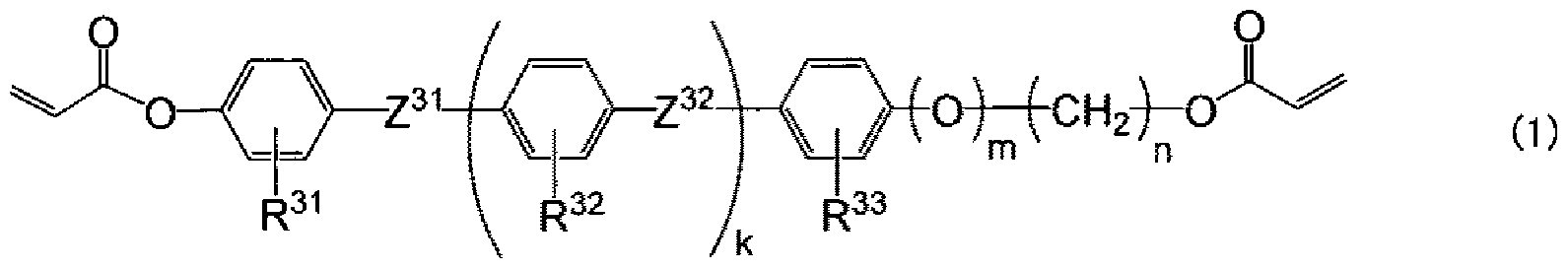


Claims


Priority Applications (2)
| Application Number | Priority Date | Filing Date | Title |
|---|---|---|---|
| US11/914,612 US7907247B2 (en) | 2005-05-19 | 2006-05-18 | Liquid crystal display |
| EP06746626A EP1890187A4 (en) | 2005-05-19 | 2006-05-18 | LIQUID CRYSTAL DISPLAY ELEMENT |
Applications Claiming Priority (2)
| Application Number | Priority Date | Filing Date | Title |
|---|---|---|---|
| JP2005-147327 | 2005-05-19 | ||
| JP2005147327 | 2005-05-19 |
Publications (1)
| Publication Number | Publication Date |
|---|---|
| WO2006123749A1 true WO2006123749A1 (ja) | 2006-11-23 |
Family
ID=37431321
Family Applications (1)
| Application Number | Title | Priority Date | Filing Date |
|---|---|---|---|
| PCT/JP2006/309959 WO2006123749A1 (ja) | 2005-05-19 | 2006-05-18 | 液晶表示素子 |
Country Status (6)
| Country | Link |
|---|---|
| US (1) | US7907247B2 (ja) |
| EP (1) | EP1890187A4 (ja) |
| JP (1) | JP5402999B2 (ja) |
| KR (1) | KR101021696B1 (ja) |
| CN (1) | CN100565300C (ja) |
| WO (1) | WO2006123749A1 (ja) |
Cited By (8)
| Publication number | Priority date | Publication date | Assignee | Title |
|---|---|---|---|---|
| WO2008062744A1 (fr) * | 2006-11-24 | 2008-05-29 | Dai Nippon Printing Co., Ltd. | Elément d'affichage à cristaux liquides |
| JP2009230069A (ja) * | 2008-03-25 | 2009-10-08 | Dainippon Printing Co Ltd | 液晶表示素子 |
| US7907247B2 (en) | 2005-05-19 | 2011-03-15 | Dai Nippon Printing Co., Ltd. | Liquid crystal display |
| CN102081255A (zh) * | 2010-11-25 | 2011-06-01 | 华映视讯(吴江)有限公司 | 立体显示装置及其制作方法 |
| WO2012050179A1 (ja) * | 2010-10-14 | 2012-04-19 | シャープ株式会社 | 液晶表示装置の製造方法 |
| WO2012050177A1 (ja) * | 2010-10-14 | 2012-04-19 | シャープ株式会社 | 液晶表示装置及び液晶表示装置の製造方法 |
| CN103472521A (zh) * | 2007-04-16 | 2013-12-25 | 北卡罗莱纳州立大学 | 低扭曲手性液晶偏振光栅和相关制造方法 |
| US9798179B2 (en) | 2010-10-14 | 2017-10-24 | Merck Patent Gmbh | Liquid crystal display device |
Families Citing this family (12)
| Publication number | Priority date | Publication date | Assignee | Title |
|---|---|---|---|---|
| KR101641535B1 (ko) * | 2009-06-01 | 2016-07-22 | 삼성디스플레이 주식회사 | 액정표시패널의 제조 방법 및 액정표시패널 |
| KR101615926B1 (ko) * | 2009-07-28 | 2016-04-28 | 삼성디스플레이 주식회사 | 액정표시장치 및 이의 제조방법 |
| CN103097945B (zh) * | 2010-08-03 | 2015-09-30 | 夏普株式会社 | 液晶显示装置及液晶显示装置的制造方法 |
| TW201215970A (en) * | 2010-10-04 | 2012-04-16 | Chunghwa Picture Tubes Ltd | Liquid crystal alignment process |
| JP2012113215A (ja) * | 2010-11-26 | 2012-06-14 | Stanley Electric Co Ltd | 液晶素子 |
| KR101757330B1 (ko) * | 2011-01-17 | 2017-07-13 | 삼성디스플레이 주식회사 | 액정 표시 장치 |
| CN103403127A (zh) * | 2011-03-30 | 2013-11-20 | 株式会社艾迪科 | 聚合性液晶组合物、偏振发光性涂料、新型萘内酰胺衍生物、新型香豆素衍生物、新型尼罗红衍生物以及新型蒽衍生物 |
| KR20130017938A (ko) * | 2011-08-12 | 2013-02-20 | 주식회사 동진쎄미켐 | 중합성 액정 조성물 |
| CN106873248B (zh) * | 2011-08-31 | 2020-11-03 | 夏普株式会社 | 液晶显示面板和液晶显示装置 |
| CN102650759B (zh) * | 2012-01-06 | 2014-11-05 | 京东方科技集团股份有限公司 | 一种液晶面板及其制造方法 |
| CN104570486A (zh) * | 2013-10-30 | 2015-04-29 | 京东方科技集团股份有限公司 | 一种配向膜的制作方法 |
| WO2016150393A1 (en) * | 2015-03-24 | 2016-09-29 | The Hong Kong University Of Science And Technology | Optically addressed multi-stable full color liquid crystal display |
Citations (4)
| Publication number | Priority date | Publication date | Assignee | Title |
|---|---|---|---|---|
| US20020085153A1 (en) | 2000-12-30 | 2002-07-04 | Choi Suk Won | Ferroelectric liquid crystal display |
| JP2002532755A (ja) | 1998-12-15 | 2002-10-02 | ロリク アーゲー | 液晶材料用配向層 |
| JP2003029237A (ja) * | 2001-07-16 | 2003-01-29 | Fujitsu Ltd | 液晶表示素子 |
| JP2003241226A (ja) * | 2002-02-19 | 2003-08-27 | Fujitsu Ltd | 液晶表示素子 |
Family Cites Families (40)
| Publication number | Priority date | Publication date | Assignee | Title |
|---|---|---|---|---|
| JPH06105332B2 (ja) | 1986-02-06 | 1994-12-21 | 旭硝子株式会社 | 強誘電性液晶光シヤツタ− |
| JPS62275223A (ja) | 1986-05-23 | 1987-11-30 | Canon Inc | 液晶素子及びその駆動法 |
| JP2667816B2 (ja) | 1986-09-20 | 1997-10-27 | キヤノン株式会社 | 液晶素子 |
| JPH01105912A (ja) | 1987-10-19 | 1989-04-24 | Seiko Epson Corp | 液晶電気光学素子 |
| NL9001643A (nl) | 1990-07-19 | 1992-02-17 | Philips Nv | Werkwijze voor het aanbrengen van een orientatielaag in een vloeibaar kristallijne beeldweergeefcel. |
| EP0506175B1 (en) | 1991-03-26 | 1996-12-04 | Koninklijke Philips Electronics N.V. | Liquid crystal display device comprising an orientation layer |
| JPH0764051A (ja) | 1993-08-27 | 1995-03-10 | Sharp Corp | 液晶表示装置およびその駆動方法 |
| JPH07128640A (ja) | 1993-10-29 | 1995-05-19 | Sharp Corp | 強誘電性液晶表示装置 |
| JPH07199202A (ja) | 1993-12-27 | 1995-08-04 | Toppan Printing Co Ltd | 強誘電性液晶または反強誘電性液晶表示素子とその製造方法 |
| JPH07239485A (ja) | 1994-02-28 | 1995-09-12 | Semiconductor Energy Lab Co Ltd | 電子スチルカメラ用シャッターおよびそれを用いた電子スチルカメラ |
| GB2293889A (en) * | 1994-10-03 | 1996-04-10 | Sharp Kk | Liquid crystal device and method of making a liquid crystal device |
| JPH09127525A (ja) | 1995-11-06 | 1997-05-16 | Sharp Corp | 液晶表示素子およびその製造方法 |
| TW400452B (en) | 1995-12-27 | 2000-08-01 | Sharp Kk | Liquid crystal display element and a manufacturing method thereof as well as a liquid crystal display |
| JP2000010076A (ja) | 1998-06-24 | 2000-01-14 | Canon Inc | 液晶素子 |
| JP3311335B2 (ja) | 1999-08-27 | 2002-08-05 | キヤノン株式会社 | 液晶素子及びこれを用いた表示装置、該液晶素子の駆動方法 |
| JP2002023164A (ja) | 2000-07-04 | 2002-01-23 | Nec Corp | 液晶表示方法、液晶表示装置、及び、それの製造装置 |
| JP4674738B2 (ja) * | 2001-01-31 | 2011-04-20 | 駿介 小林 | 液晶表示素子の製造方法 |
| JP2003005223A (ja) | 2001-06-25 | 2003-01-08 | Science Univ Of Tokyo | 高コントラスト比非対称電気光学特性液晶表示素子の製造方法 |
| US20030021913A1 (en) | 2001-07-03 | 2003-01-30 | O'neill Mary | Liquid crystal alignment layer |
| JP4040377B2 (ja) | 2001-07-16 | 2008-01-30 | 株式会社半導体エネルギー研究所 | 液晶表示装置の作製方法 |
| KR100412489B1 (ko) * | 2001-10-10 | 2003-12-31 | 삼성전자주식회사 | 강유전성 액정 표시장치 및 그 구동방법 |
| JP2003172935A (ja) | 2001-12-07 | 2003-06-20 | Seiko Epson Corp | 液晶装置、液晶装置の製造方法、及び電子機器 |
| GB2388201A (en) | 2002-04-30 | 2003-11-05 | Hewlett Packard Co | Liquid crystal device |
| JP2004013098A (ja) | 2002-06-11 | 2004-01-15 | Fujitsu Ltd | 液晶表示装置及びその製造方法 |
| JP2004012543A (ja) | 2002-06-03 | 2004-01-15 | Canon Inc | 液晶素子、及び該液晶素子を備えた液晶装置 |
| JP2004078099A (ja) | 2002-08-22 | 2004-03-11 | Canon Inc | 液晶素子の製造方法 |
| JP2004145258A (ja) | 2002-08-30 | 2004-05-20 | Fujitsu Ltd | 液晶表示装置の製造方法及び液晶表示装置 |
| JP4220748B2 (ja) | 2002-09-20 | 2009-02-04 | 日本放送協会 | 液晶表示素子、液晶表示素子の製造方法および液晶表示装置 |
| DE602005024519D1 (de) | 2004-01-22 | 2010-12-16 | Dainippon Printing Co Ltd | Flüssigkristallanzeigeeinrichtung |
| JP4537718B2 (ja) | 2004-01-22 | 2010-09-08 | 大日本印刷株式会社 | 液晶表示素子 |
| JP4520314B2 (ja) | 2004-01-22 | 2010-08-04 | 大日本印刷株式会社 | 液晶表示素子 |
| US7553521B2 (en) * | 2004-01-22 | 2009-06-30 | Dai Nippon Printing Co., Ltd. | Liquid crystal displays |
| KR101066784B1 (ko) | 2004-02-10 | 2011-09-21 | 다이니폰 인사츠 가부시키가이샤 | 액정 표시 소자 |
| JP4528645B2 (ja) | 2004-02-10 | 2010-08-18 | 大日本印刷株式会社 | 液晶表示素子 |
| JP4676214B2 (ja) | 2004-02-10 | 2011-04-27 | 大日本印刷株式会社 | 液晶表示素子 |
| US7402332B2 (en) * | 2004-02-10 | 2008-07-22 | Dai Nippon Printing Co., Ltd. | Liquid crystal display |
| US7777847B2 (en) | 2004-06-11 | 2010-08-17 | Dai Nippon Printing Co., Ltd. | Liquid crystal display and manufacturing method of the same |
| US7499135B2 (en) * | 2004-06-11 | 2009-03-03 | Dai Nippon Printing Co., Ltd. | Liquid crystal display |
| WO2006123749A1 (ja) | 2005-05-19 | 2006-11-23 | Dai Nippon Printing Co., Ltd. | 液晶表示素子 |
| JP2006323223A (ja) | 2005-05-19 | 2006-11-30 | Dainippon Printing Co Ltd | 液晶表示素子 |
-
2006
- 2006-05-18 WO PCT/JP2006/309959 patent/WO2006123749A1/ja active Application Filing
- 2006-05-18 KR KR1020077029588A patent/KR101021696B1/ko not_active IP Right Cessation
- 2006-05-18 US US11/914,612 patent/US7907247B2/en not_active Expired - Fee Related
- 2006-05-18 CN CNB2006800173466A patent/CN100565300C/zh not_active Expired - Fee Related
- 2006-05-18 EP EP06746626A patent/EP1890187A4/en not_active Withdrawn
-
2011
- 2011-07-01 JP JP2011147603A patent/JP5402999B2/ja not_active Expired - Fee Related
Patent Citations (4)
| Publication number | Priority date | Publication date | Assignee | Title |
|---|---|---|---|---|
| JP2002532755A (ja) | 1998-12-15 | 2002-10-02 | ロリク アーゲー | 液晶材料用配向層 |
| US20020085153A1 (en) | 2000-12-30 | 2002-07-04 | Choi Suk Won | Ferroelectric liquid crystal display |
| JP2003029237A (ja) * | 2001-07-16 | 2003-01-29 | Fujitsu Ltd | 液晶表示素子 |
| JP2003241226A (ja) * | 2002-02-19 | 2003-08-27 | Fujitsu Ltd | 液晶表示素子 |
Non-Patent Citations (3)
| Title |
|---|
| NONAKA, T.; LI, J.; OGAWA, A.; HORNUNG, B.; SCHMIDT, W.; WINGEN, R.; DUBAL, H., LIQ. CRYST., vol. 26, 1999, pages 1599 |
| PATEL, J.; GOODBY, J. W., J. APPL. PHYS., vol. 59, 1986, pages 2355 |
| See also references of EP1890187A4 |
Cited By (11)
| Publication number | Priority date | Publication date | Assignee | Title |
|---|---|---|---|---|
| US7907247B2 (en) | 2005-05-19 | 2011-03-15 | Dai Nippon Printing Co., Ltd. | Liquid crystal display |
| WO2008062744A1 (fr) * | 2006-11-24 | 2008-05-29 | Dai Nippon Printing Co., Ltd. | Elément d'affichage à cristaux liquides |
| JP2008129529A (ja) * | 2006-11-24 | 2008-06-05 | Dainippon Printing Co Ltd | 液晶表示素子 |
| US8130358B2 (en) | 2006-11-24 | 2012-03-06 | Dai Nippon Printing Co., Ltd. | Liquid crystal display |
| CN103472521A (zh) * | 2007-04-16 | 2013-12-25 | 北卡罗莱纳州立大学 | 低扭曲手性液晶偏振光栅和相关制造方法 |
| JP2009230069A (ja) * | 2008-03-25 | 2009-10-08 | Dainippon Printing Co Ltd | 液晶表示素子 |
| WO2012050179A1 (ja) * | 2010-10-14 | 2012-04-19 | シャープ株式会社 | 液晶表示装置の製造方法 |
| WO2012050177A1 (ja) * | 2010-10-14 | 2012-04-19 | シャープ株式会社 | 液晶表示装置及び液晶表示装置の製造方法 |
| US9557605B2 (en) | 2010-10-14 | 2017-01-31 | Merck Patent Gmbh | Method of producing liquid crystal display device |
| US9798179B2 (en) | 2010-10-14 | 2017-10-24 | Merck Patent Gmbh | Liquid crystal display device |
| CN102081255A (zh) * | 2010-11-25 | 2011-06-01 | 华映视讯(吴江)有限公司 | 立体显示装置及其制作方法 |
Also Published As
| Publication number | Publication date |
|---|---|
| JP5402999B2 (ja) | 2014-01-29 |
| KR20080027778A (ko) | 2008-03-28 |
| CN101180567A (zh) | 2008-05-14 |
| EP1890187A1 (en) | 2008-02-20 |
| JP2011248368A (ja) | 2011-12-08 |
| US20090051854A1 (en) | 2009-02-26 |
| US7907247B2 (en) | 2011-03-15 |
| EP1890187A4 (en) | 2009-04-22 |
| CN100565300C (zh) | 2009-12-02 |
| KR101021696B1 (ko) | 2011-03-15 |
Similar Documents
| Publication | Publication Date | Title |
|---|---|---|
| JP5402999B2 (ja) | 液晶表示素子 | |
| US8009266B2 (en) | Process for producing liquid crystal display | |
| KR101066784B1 (ko) | 액정 표시 소자 | |
| JP4528645B2 (ja) | 液晶表示素子 | |
| KR101073722B1 (ko) | 액정 표시 소자 | |
| US7402332B2 (en) | Liquid crystal display | |
| US7911562B2 (en) | Liquid crystal display and process for producing the same | |
| US7892449B2 (en) | Liquid crystal display and manufacturing method of same | |
| JP2005234550A (ja) | 液晶表示素子 | |
| JP4844013B2 (ja) | 液晶表示素子の製造方法 | |
| JP5062182B2 (ja) | 液晶表示素子 | |
| JP4676214B2 (ja) | 液晶表示素子 | |
| JP4839959B2 (ja) | 液晶表示素子 | |
| JP2006323223A (ja) | 液晶表示素子 | |
| JP2005258429A (ja) | 液晶表示素子 | |
| JP2006330309A (ja) | 液晶表示素子 | |
| JP4888049B2 (ja) | 液晶表示素子 | |
| JP4862281B2 (ja) | 液晶表示素子 | |
| JP2006330310A (ja) | 液晶表示素子 | |
| WO2005124440A1 (ja) | 液晶表示素子 | |
| JP5391538B2 (ja) | 液晶表示素子の製造方法 | |
| JP4992198B2 (ja) | 液晶表示素子および液晶表示素子の製造方法 | |
| JP2010230886A (ja) | 液晶表示素子 | |
| JP2012053491A (ja) | 液晶表示素子および液晶表示素子の製造方法 |
Legal Events
| Date | Code | Title | Description |
|---|---|---|---|
| WWE | Wipo information: entry into national phase |
Ref document number: 200680017346.6 Country of ref document: CN |
|
| 121 | Ep: the epo has been informed by wipo that ep was designated in this application | ||
| WWE | Wipo information: entry into national phase |
Ref document number: 11914612 Country of ref document: US |
|
| NENP | Non-entry into the national phase |
Ref country code: DE |
|
| WWE | Wipo information: entry into national phase |
Ref document number: 2006746626 Country of ref document: EP Ref document number: 1020077029588 Country of ref document: KR |
|
| NENP | Non-entry into the national phase |
Ref country code: RU |
|
| WWP | Wipo information: published in national office |
Ref document number: 2006746626 Country of ref document: EP |