WO2005090512A1 - New materials for injecting or transporting holes and organic electroluminescence devices using the same - Google Patents
New materials for injecting or transporting holes and organic electroluminescence devices using the same Download PDFInfo
- Publication number
- WO2005090512A1 WO2005090512A1 PCT/KR2005/000794 KR2005000794W WO2005090512A1 WO 2005090512 A1 WO2005090512 A1 WO 2005090512A1 KR 2005000794 W KR2005000794 W KR 2005000794W WO 2005090512 A1 WO2005090512 A1 WO 2005090512A1
- Authority
- WO
- WIPO (PCT)
- Prior art keywords
- formula
- mmol
- compound
- light emitting
- compound represented
- Prior art date
Links
- 238000005401 electroluminescence Methods 0.000 title abstract description 62
- 239000000463 material Substances 0.000 title description 58
- 150000001875 compounds Chemical class 0.000 claims abstract description 210
- 150000002894 organic compounds Chemical class 0.000 claims abstract description 18
- 238000002347 injection Methods 0.000 claims description 46
- 239000007924 injection Substances 0.000 claims description 46
- 230000005525 hole transport Effects 0.000 claims description 41
- 125000000217 alkyl group Chemical group 0.000 claims description 12
- -1 heteroaromatic hydrocarbon Chemical class 0.000 claims description 12
- 150000004945 aromatic hydrocarbons Chemical class 0.000 claims description 9
- RAXXELZNTBOGNW-UHFFFAOYSA-N imidazole Natural products C1=CNC=N1 RAXXELZNTBOGNW-UHFFFAOYSA-N 0.000 claims description 9
- 239000000758 substrate Substances 0.000 claims description 9
- YTPLMLYBLZKORZ-UHFFFAOYSA-N Thiophene Chemical group C=1C=CSC=1 YTPLMLYBLZKORZ-UHFFFAOYSA-N 0.000 claims description 8
- 125000003277 amino group Chemical group 0.000 claims description 7
- 229910052736 halogen Inorganic materials 0.000 claims description 7
- 150000002367 halogens Chemical class 0.000 claims description 7
- 229930195733 hydrocarbon Natural products 0.000 claims description 7
- 239000004215 Carbon black (E152) Substances 0.000 claims description 6
- YLQBMQCUIZJEEH-UHFFFAOYSA-N Furan Chemical compound C=1C=COC=1 YLQBMQCUIZJEEH-UHFFFAOYSA-N 0.000 claims description 6
- KYQCOXFCLRTKLS-UHFFFAOYSA-N Pyrazine Chemical compound C1=CN=CC=N1 KYQCOXFCLRTKLS-UHFFFAOYSA-N 0.000 claims description 6
- KAESVJOAVNADME-UHFFFAOYSA-N Pyrrole Chemical compound C=1C=CNC=1 KAESVJOAVNADME-UHFFFAOYSA-N 0.000 claims description 6
- SMWDFEZZVXVKRB-UHFFFAOYSA-N Quinoline Chemical compound N1=CC=CC2=CC=CC=C21 SMWDFEZZVXVKRB-UHFFFAOYSA-N 0.000 claims description 6
- 125000003545 alkoxy group Chemical group 0.000 claims description 6
- ZUOUZKKEUPVFJK-UHFFFAOYSA-N diphenyl Chemical compound C1=CC=CC=C1C1=CC=CC=C1 ZUOUZKKEUPVFJK-UHFFFAOYSA-N 0.000 claims description 6
- 125000004435 hydrogen atom Chemical group [H]* 0.000 claims description 6
- AWJUIBRHMBBTKR-UHFFFAOYSA-N isoquinoline Chemical compound C1=NC=CC2=CC=CC=C21 AWJUIBRHMBBTKR-UHFFFAOYSA-N 0.000 claims description 6
- 150000002825 nitriles Chemical class 0.000 claims description 6
- 125000000449 nitro group Chemical group [O-][N+](*)=O 0.000 claims description 6
- 150000001338 aliphatic hydrocarbons Chemical class 0.000 claims description 5
- 125000002080 perylenyl group Chemical group C1(=CC=C2C=CC=C3C4=CC=CC5=CC=CC(C1=C23)=C45)* 0.000 claims description 5
- YJTKZCDBKVTVBY-UHFFFAOYSA-N 1,3-Diphenylbenzene Chemical group C1=CC=CC=C1C1=CC=CC(C=2C=CC=CC=2)=C1 YJTKZCDBKVTVBY-UHFFFAOYSA-N 0.000 claims description 3
- ZCQWOFVYLHDMMC-UHFFFAOYSA-N Oxazole Chemical compound C1=COC=N1 ZCQWOFVYLHDMMC-UHFFFAOYSA-N 0.000 claims description 3
- PCNDJXKNXGMECE-UHFFFAOYSA-N Phenazine Natural products C1=CC=CC2=NC3=CC=CC=C3N=C21 PCNDJXKNXGMECE-UHFFFAOYSA-N 0.000 claims description 3
- FZWLAAWBMGSTSO-UHFFFAOYSA-N Thiazole Chemical compound C1=CSC=N1 FZWLAAWBMGSTSO-UHFFFAOYSA-N 0.000 claims description 3
- 235000010290 biphenyl Nutrition 0.000 claims description 3
- 239000004305 biphenyl Substances 0.000 claims description 3
- 125000004432 carbon atom Chemical group C* 0.000 claims description 3
- 125000001624 naphthyl group Chemical group 0.000 claims description 3
- WCPAKWJPBJAGKN-UHFFFAOYSA-N oxadiazole Chemical compound C1=CON=N1 WCPAKWJPBJAGKN-UHFFFAOYSA-N 0.000 claims description 3
- YNPNZTXNASCQKK-UHFFFAOYSA-N phenanthrene Chemical compound C1=CC=C2C3=CC=CC=C3C=CC2=C1 YNPNZTXNASCQKK-UHFFFAOYSA-N 0.000 claims description 3
- 125000001997 phenyl group Chemical group [H]C1=C([H])C([H])=C(*)C([H])=C1[H] 0.000 claims description 3
- 125000001725 pyrenyl group Chemical group 0.000 claims description 3
- 125000005495 pyridazyl group Chemical group 0.000 claims description 3
- 125000004076 pyridyl group Chemical group 0.000 claims description 3
- VLLMWSRANPNYQX-UHFFFAOYSA-N thiadiazole Chemical compound C1=CSN=N1.C1=CSN=N1 VLLMWSRANPNYQX-UHFFFAOYSA-N 0.000 claims description 3
- 229930192474 thiophene Natural products 0.000 claims description 3
- 150000003852 triazoles Chemical class 0.000 claims description 3
- ZOXJGFHDIHLPTG-UHFFFAOYSA-N Boron Chemical group [B] ZOXJGFHDIHLPTG-UHFFFAOYSA-N 0.000 claims description 2
- XUIMIQQOPSSXEZ-UHFFFAOYSA-N Silicon Chemical group [Si] XUIMIQQOPSSXEZ-UHFFFAOYSA-N 0.000 claims description 2
- 125000002178 anthracenyl group Chemical group C1(=CC=CC2=CC3=CC=CC=C3C=C12)* 0.000 claims description 2
- 125000006615 aromatic heterocyclic group Chemical group 0.000 claims description 2
- UREZNYTWGJKWBI-UHFFFAOYSA-M benzethonium chloride Chemical compound [Cl-].C1=CC(C(C)(C)CC(C)(C)C)=CC=C1OCCOCC[N+](C)(C)CC1=CC=CC=C1 UREZNYTWGJKWBI-UHFFFAOYSA-M 0.000 claims description 2
- 235000013350 formula milk Nutrition 0.000 description 427
- XEKOWRVHYACXOJ-UHFFFAOYSA-N Ethyl acetate Chemical compound CCOC(C)=O XEKOWRVHYACXOJ-UHFFFAOYSA-N 0.000 description 117
- 239000010410 layer Substances 0.000 description 98
- VLKZOEOYAKHREP-UHFFFAOYSA-N n-Hexane Chemical compound CCCCCC VLKZOEOYAKHREP-UHFFFAOYSA-N 0.000 description 88
- WYURNTSHIVDZCO-UHFFFAOYSA-N Tetrahydrofuran Chemical compound C1CCOC1 WYURNTSHIVDZCO-UHFFFAOYSA-N 0.000 description 82
- 239000011541 reaction mixture Substances 0.000 description 70
- MFRIHAYPQRLWNB-UHFFFAOYSA-N sodium tert-butoxide Chemical compound [Na+].CC(C)(C)[O-] MFRIHAYPQRLWNB-UHFFFAOYSA-N 0.000 description 62
- 239000000047 product Substances 0.000 description 59
- 238000004440 column chromatography Methods 0.000 description 44
- 238000002360 preparation method Methods 0.000 description 42
- 238000006243 chemical reaction Methods 0.000 description 41
- 238000004519 manufacturing process Methods 0.000 description 39
- KDLHZDBZIXYQEI-UHFFFAOYSA-N Palladium Chemical compound [Pd] KDLHZDBZIXYQEI-UHFFFAOYSA-N 0.000 description 34
- 239000000203 mixture Substances 0.000 description 34
- CTQNGGLPUBDAKN-UHFFFAOYSA-N O-Xylene Chemical compound CC1=CC=CC=C1C CTQNGGLPUBDAKN-UHFFFAOYSA-N 0.000 description 32
- 239000012044 organic layer Substances 0.000 description 32
- 239000008096 xylene Substances 0.000 description 32
- 229910052943 magnesium sulfate Inorganic materials 0.000 description 31
- 239000011259 mixed solution Substances 0.000 description 30
- YMWUJEATGCHHMB-UHFFFAOYSA-N Dichloromethane Chemical compound ClCCl YMWUJEATGCHHMB-UHFFFAOYSA-N 0.000 description 27
- 239000007858 starting material Substances 0.000 description 24
- HEMHJVSKTPXQMS-UHFFFAOYSA-M Sodium hydroxide Chemical compound [OH-].[Na+] HEMHJVSKTPXQMS-UHFFFAOYSA-M 0.000 description 21
- 230000005684 electric field Effects 0.000 description 21
- 230000032258 transport Effects 0.000 description 21
- 238000001228 spectrum Methods 0.000 description 20
- LFQSCWFLJHTTHZ-UHFFFAOYSA-N Ethanol Chemical compound CCO LFQSCWFLJHTTHZ-UHFFFAOYSA-N 0.000 description 18
- YXFVVABEGXRONW-UHFFFAOYSA-N Toluene Chemical compound CC1=CC=CC=C1 YXFVVABEGXRONW-UHFFFAOYSA-N 0.000 description 18
- XLYOFNOQVPJJNP-UHFFFAOYSA-N water Substances O XLYOFNOQVPJJNP-UHFFFAOYSA-N 0.000 description 17
- HEDRZPFGACZZDS-MICDWDOJSA-N Trichloro(2H)methane Chemical compound [2H]C(Cl)(Cl)Cl HEDRZPFGACZZDS-MICDWDOJSA-N 0.000 description 15
- 238000000034 method Methods 0.000 description 15
- 239000011368 organic material Substances 0.000 description 15
- 239000000243 solution Substances 0.000 description 15
- HEDRZPFGACZZDS-UHFFFAOYSA-N Chloroform Chemical compound ClC(Cl)Cl HEDRZPFGACZZDS-UHFFFAOYSA-N 0.000 description 12
- CSNNHWWHGAXBCP-UHFFFAOYSA-L Magnesium sulfate Chemical compound [Mg+2].[O-][S+2]([O-])([O-])[O-] CSNNHWWHGAXBCP-UHFFFAOYSA-L 0.000 description 12
- DTQVDTLACAAQTR-UHFFFAOYSA-N Trifluoroacetic acid Chemical compound OC(=O)C(F)(F)F DTQVDTLACAAQTR-UHFFFAOYSA-N 0.000 description 12
- DYHSDKLCOJIUFX-UHFFFAOYSA-N tert-butoxycarbonyl anhydride Chemical compound CC(C)(C)OC(=O)OC(=O)OC(C)(C)C DYHSDKLCOJIUFX-UHFFFAOYSA-N 0.000 description 12
- 238000001771 vacuum deposition Methods 0.000 description 12
- 125000000609 carbazolyl group Chemical group C1(=CC=CC=2C3=CC=CC=C3NC12)* 0.000 description 10
- TVIVIEFSHFOWTE-UHFFFAOYSA-K tri(quinolin-8-yloxy)alumane Chemical compound [Al+3].C1=CN=C2C([O-])=CC=CC2=C1.C1=CN=C2C([O-])=CC=CC2=C1.C1=CN=C2C([O-])=CC=CC2=C1 TVIVIEFSHFOWTE-UHFFFAOYSA-K 0.000 description 10
- 0 CCC=C*CC(CC)=C[C@@]1C2=CCCC=C2C(C)=*(C)CC1 Chemical compound CCC=C*CC(CC)=C[C@@]1C2=CCCC=C2C(C)=*(C)CC1 0.000 description 9
- ZMXDDKWLCZADIW-UHFFFAOYSA-N N,N-Dimethylformamide Chemical compound CN(C)C=O ZMXDDKWLCZADIW-UHFFFAOYSA-N 0.000 description 9
- 125000003118 aryl group Chemical group 0.000 description 9
- 230000008569 process Effects 0.000 description 9
- UJOBWOGCFQCDNV-UHFFFAOYSA-N 9H-carbazole Chemical compound C1=CC=C2C3=CC=CC=C3NC2=C1 UJOBWOGCFQCDNV-UHFFFAOYSA-N 0.000 description 8
- KEQFTVQCIQJIQW-UHFFFAOYSA-N N-Phenyl-2-naphthylamine Chemical compound C=1C=C2C=CC=CC2=CC=1NC1=CC=CC=C1 KEQFTVQCIQJIQW-UHFFFAOYSA-N 0.000 description 8
- PCLIMKBDDGJMGD-UHFFFAOYSA-N N-bromosuccinimide Chemical compound BrN1C(=O)CCC1=O PCLIMKBDDGJMGD-UHFFFAOYSA-N 0.000 description 8
- 238000005481 NMR spectroscopy Methods 0.000 description 8
- DMBHHRLKUKUOEG-UHFFFAOYSA-N diphenylamine Chemical compound C=1C=CC=CC=1NC1=CC=CC=C1 DMBHHRLKUKUOEG-UHFFFAOYSA-N 0.000 description 8
- 229910052751 metal Inorganic materials 0.000 description 8
- 239000002184 metal Substances 0.000 description 8
- 238000005160 1H NMR spectroscopy Methods 0.000 description 7
- 125000001424 substituent group Chemical group 0.000 description 7
- RFFLAFLAYFXFSW-UHFFFAOYSA-N 1,2-dichlorobenzene Chemical compound ClC1=CC=CC=C1Cl RFFLAFLAYFXFSW-UHFFFAOYSA-N 0.000 description 6
- VHYFNPMBLIVWCW-UHFFFAOYSA-N 4-Dimethylaminopyridine Chemical compound CN(C)C1=CC=NC=C1 VHYFNPMBLIVWCW-UHFFFAOYSA-N 0.000 description 6
- 239000012043 crude product Substances 0.000 description 6
- 235000019341 magnesium sulphate Nutrition 0.000 description 6
- NFHFRUOZVGFOOS-UHFFFAOYSA-N palladium;triphenylphosphane Chemical compound [Pd].C1=CC=CC=C1P(C=1C=CC=CC=1)C1=CC=CC=C1.C1=CC=CC=C1P(C=1C=CC=CC=1)C1=CC=CC=C1.C1=CC=CC=C1P(C=1C=CC=CC=1)C1=CC=CC=C1.C1=CC=CC=C1P(C=1C=CC=CC=1)C1=CC=CC=C1 NFHFRUOZVGFOOS-UHFFFAOYSA-N 0.000 description 6
- 239000010409 thin film Substances 0.000 description 6
- 229910052782 aluminium Inorganic materials 0.000 description 5
- XAGFODPZIPBFFR-UHFFFAOYSA-N aluminium Chemical compound [Al] XAGFODPZIPBFFR-UHFFFAOYSA-N 0.000 description 5
- 150000001412 amines Chemical class 0.000 description 5
- 230000009477 glass transition Effects 0.000 description 5
- 125000005843 halogen group Chemical group 0.000 description 5
- 150000002739 metals Chemical class 0.000 description 5
- 239000002244 precipitate Substances 0.000 description 5
- 239000010949 copper Substances 0.000 description 4
- 239000012153 distilled water Substances 0.000 description 4
- 239000000706 filtrate Substances 0.000 description 4
- 239000004973 liquid crystal related substance Substances 0.000 description 4
- PQXKHYXIUOZZFA-UHFFFAOYSA-M lithium fluoride Chemical compound [Li+].[F-] PQXKHYXIUOZZFA-UHFFFAOYSA-M 0.000 description 4
- 238000005406 washing Methods 0.000 description 4
- XEZNGIUYQVAUSS-UHFFFAOYSA-N 18-crown-6 Chemical compound C1COCCOCCOCCOCCOCCO1 XEZNGIUYQVAUSS-UHFFFAOYSA-N 0.000 description 3
- QPTWWBLGJZWRAV-UHFFFAOYSA-N 2,7-dibromo-9h-carbazole Chemical compound BrC1=CC=C2C3=CC=C(Br)C=C3NC2=C1 QPTWWBLGJZWRAV-UHFFFAOYSA-N 0.000 description 3
- TWPMMLHBHPYSMT-UHFFFAOYSA-N 3-methyl-n-phenylaniline Chemical compound CC1=CC=CC(NC=2C=CC=CC=2)=C1 TWPMMLHBHPYSMT-UHFFFAOYSA-N 0.000 description 3
- CSCPPACGZOOCGX-UHFFFAOYSA-N Acetone Chemical compound CC(C)=O CSCPPACGZOOCGX-UHFFFAOYSA-N 0.000 description 3
- KFZMGEQAYNKOFK-UHFFFAOYSA-N Isopropanol Chemical compound CC(C)O KFZMGEQAYNKOFK-UHFFFAOYSA-N 0.000 description 3
- OKKJLVBELUTLKV-UHFFFAOYSA-N Methanol Chemical compound OC OKKJLVBELUTLKV-UHFFFAOYSA-N 0.000 description 3
- XQVWYOYUZDUNRW-UHFFFAOYSA-N N-Phenyl-1-naphthylamine Chemical compound C=1C=CC2=CC=CC=C2C=1NC1=CC=CC=C1 XQVWYOYUZDUNRW-UHFFFAOYSA-N 0.000 description 3
- 238000010521 absorption reaction Methods 0.000 description 3
- 150000001491 aromatic compounds Chemical class 0.000 description 3
- 230000015572 biosynthetic process Effects 0.000 description 3
- 239000012267 brine Substances 0.000 description 3
- 230000000694 effects Effects 0.000 description 3
- 239000011521 glass Substances 0.000 description 3
- ABMCIJZTMPDEGW-UHFFFAOYSA-N n-(4-bromophenyl)-n-phenylnaphthalen-1-amine Chemical compound C1=CC(Br)=CC=C1N(C=1C2=CC=CC=C2C=CC=1)C1=CC=CC=C1 ABMCIJZTMPDEGW-UHFFFAOYSA-N 0.000 description 3
- 229910000027 potassium carbonate Inorganic materials 0.000 description 3
- TYJJADVDDVDEDZ-UHFFFAOYSA-M potassium hydrogencarbonate Chemical compound [K+].OC([O-])=O TYJJADVDDVDEDZ-UHFFFAOYSA-M 0.000 description 3
- 238000010992 reflux Methods 0.000 description 3
- HPALAKNZSZLMCH-UHFFFAOYSA-M sodium;chloride;hydrate Chemical compound O.[Na+].[Cl-] HPALAKNZSZLMCH-UHFFFAOYSA-M 0.000 description 3
- QBLFZIBJXUQVRF-UHFFFAOYSA-N (4-bromophenyl)boronic acid Chemical compound OB(O)C1=CC=C(Br)C=C1 QBLFZIBJXUQVRF-UHFFFAOYSA-N 0.000 description 2
- FIHILUSWISKVSR-UHFFFAOYSA-N 3,6-dibromo-9h-carbazole Chemical compound C1=C(Br)C=C2C3=CC(Br)=CC=C3NC2=C1 FIHILUSWISKVSR-UHFFFAOYSA-N 0.000 description 2
- QENGPZGAWFQWCZ-UHFFFAOYSA-N 3-Methylthiophene Chemical compound CC=1C=CSC=1 QENGPZGAWFQWCZ-UHFFFAOYSA-N 0.000 description 2
- REUCYFQYHWKXPH-UHFFFAOYSA-N 4-bromo-1-(4-bromo-2-nitrophenyl)-2-nitrobenzene Chemical group [O-][N+](=O)C1=CC(Br)=CC=C1C1=CC=C(Br)C=C1[N+]([O-])=O REUCYFQYHWKXPH-UHFFFAOYSA-N 0.000 description 2
- YUDBWNNTJANNOY-UHFFFAOYSA-N Cc(cc1)ccc1N(c(cc1)ccc1-[n](c(ccc(N(c1ccc(C)cc1)c1cccc2c1cccc2)c1)c1c1c2)c1ccc2N(c1ccc(C)cc1)c1cccc2c1cccc2)c1cccc2ccccc12 Chemical compound Cc(cc1)ccc1N(c(cc1)ccc1-[n](c(ccc(N(c1ccc(C)cc1)c1cccc2c1cccc2)c1)c1c1c2)c1ccc2N(c1ccc(C)cc1)c1cccc2c1cccc2)c1cccc2ccccc12 YUDBWNNTJANNOY-UHFFFAOYSA-N 0.000 description 2
- IADZLXUKYBMDAD-UHFFFAOYSA-N Cc1cc(N(c(cc2)ccc2-[n](c(ccc(N(c2cc(C)ccc2)c2cccc3c2cccc3)c2)c2c2c3)c2ccc3N(c2cccc(C)c2)c2cccc3c2cccc3)c2c(cccc3)c3ccc2)ccc1 Chemical compound Cc1cc(N(c(cc2)ccc2-[n](c(ccc(N(c2cc(C)ccc2)c2cccc3c2cccc3)c2)c2c2c3)c2ccc3N(c2cccc(C)c2)c2cccc3c2cccc3)c2c(cccc3)c3ccc2)ccc1 IADZLXUKYBMDAD-UHFFFAOYSA-N 0.000 description 2
- DGAQECJNVWCQMB-PUAWFVPOSA-M Ilexoside XXIX Chemical compound C[C@@H]1CC[C@@]2(CC[C@@]3(C(=CC[C@H]4[C@]3(CC[C@@H]5[C@@]4(CC[C@@H](C5(C)C)OS(=O)(=O)[O-])C)C)[C@@H]2[C@]1(C)O)C)C(=O)O[C@H]6[C@@H]([C@H]([C@@H]([C@H](O6)CO)O)O)O.[Na+] DGAQECJNVWCQMB-PUAWFVPOSA-M 0.000 description 2
- PXHVJJICTQNCMI-UHFFFAOYSA-N Nickel Chemical compound [Ni] PXHVJJICTQNCMI-UHFFFAOYSA-N 0.000 description 2
- NBIIXXVUZAFLBC-UHFFFAOYSA-N Phosphoric acid Chemical compound OP(O)(O)=O NBIIXXVUZAFLBC-UHFFFAOYSA-N 0.000 description 2
- MWPLVEDNUUSJAV-UHFFFAOYSA-N anthracene Chemical compound C1=CC=CC2=CC3=CC=CC=C3C=C21 MWPLVEDNUUSJAV-UHFFFAOYSA-N 0.000 description 2
- 230000008901 benefit Effects 0.000 description 2
- 150000001555 benzenes Chemical class 0.000 description 2
- 238000000576 coating method Methods 0.000 description 2
- XCJYREBRNVKWGJ-UHFFFAOYSA-N copper(II) phthalocyanine Chemical compound [Cu+2].C12=CC=CC=C2C(N=C2[N-]C(C3=CC=CC=C32)=N2)=NC1=NC([C]1C=CC=CC1=1)=NC=1N=C1[C]3C=CC=CC3=C2[N-]1 XCJYREBRNVKWGJ-UHFFFAOYSA-N 0.000 description 2
- 238000000151 deposition Methods 0.000 description 2
- 230000008021 deposition Effects 0.000 description 2
- 239000003599 detergent Substances 0.000 description 2
- 238000005516 engineering process Methods 0.000 description 2
- 230000006872 improvement Effects 0.000 description 2
- AMGQUBHHOARCQH-UHFFFAOYSA-N indium;oxotin Chemical class [In].[Sn]=O AMGQUBHHOARCQH-UHFFFAOYSA-N 0.000 description 2
- 125000000040 m-tolyl group Chemical group [H]C1=C([H])C(*)=C([H])C(=C1[H])C([H])([H])[H] 0.000 description 2
- 238000002844 melting Methods 0.000 description 2
- 230000008018 melting Effects 0.000 description 2
- 125000002950 monocyclic group Chemical group 0.000 description 2
- VWNCIFGADVGFBF-UHFFFAOYSA-N n-(3-methylphenyl)naphthalen-1-amine Chemical compound CC1=CC=CC(NC=2C3=CC=CC=C3C=CC=2)=C1 VWNCIFGADVGFBF-UHFFFAOYSA-N 0.000 description 2
- 229910052757 nitrogen Inorganic materials 0.000 description 2
- 239000002985 plastic film Substances 0.000 description 2
- 230000006798 recombination Effects 0.000 description 2
- 238000005215 recombination Methods 0.000 description 2
- 229910052708 sodium Inorganic materials 0.000 description 2
- 239000011734 sodium Substances 0.000 description 2
- 239000007787 solid Substances 0.000 description 2
- 239000011135 tin Substances 0.000 description 2
- 230000007704 transition Effects 0.000 description 2
- ZSYMVHGRKPBJCQ-UHFFFAOYSA-N 1,1'-biphenyl;9h-carbazole Chemical group C1=CC=CC=C1C1=CC=CC=C1.C1=CC=C2C3=CC=CC=C3NC2=C1 ZSYMVHGRKPBJCQ-UHFFFAOYSA-N 0.000 description 1
- KLCLIOISYBHYDZ-UHFFFAOYSA-N 1,4,4-triphenylbuta-1,3-dienylbenzene Chemical compound C=1C=CC=CC=1C(C=1C=CC=CC=1)=CC=C(C=1C=CC=CC=1)C1=CC=CC=C1 KLCLIOISYBHYDZ-UHFFFAOYSA-N 0.000 description 1
- WRGKKASJBOREMB-UHFFFAOYSA-N 1,4-dibromo-2-nitrobenzene Chemical compound [O-][N+](=O)C1=CC(Br)=CC=C1Br WRGKKASJBOREMB-UHFFFAOYSA-N 0.000 description 1
- 125000001140 1,4-phenylene group Chemical group [H]C1=C([H])C([*:2])=C([H])C([H])=C1[*:1] 0.000 description 1
- ZVFJWYZMQAEBMO-UHFFFAOYSA-N 1h-benzo[h]quinolin-10-one Chemical compound C1=CNC2=C3C(=O)C=CC=C3C=CC2=C1 ZVFJWYZMQAEBMO-UHFFFAOYSA-N 0.000 description 1
- OVSKIKFHRZPJSS-UHFFFAOYSA-N 2,4-D Chemical compound OC(=O)COC1=CC=C(Cl)C=C1Cl OVSKIKFHRZPJSS-UHFFFAOYSA-N 0.000 description 1
- KZDMFBDNQPKWNM-UHFFFAOYSA-N 2-(2-amino-4-bromophenyl)-5-bromoaniline Chemical group NC1=CC(Br)=CC=C1C1=CC=C(Br)C=C1N KZDMFBDNQPKWNM-UHFFFAOYSA-N 0.000 description 1
- 125000001622 2-naphthyl group Chemical group [H]C1=C([H])C([H])=C2C([H])=C(*)C([H])=C([H])C2=C1[H] 0.000 description 1
- CWVPIIWMONJVGG-UHFFFAOYSA-N 3-methyl-n-(3-methylphenyl)aniline Chemical compound CC1=CC=CC(NC=2C=C(C)C=CC=2)=C1 CWVPIIWMONJVGG-UHFFFAOYSA-N 0.000 description 1
- SQTLUXJWUCHKMT-UHFFFAOYSA-N 4-bromo-n,n-diphenylaniline Chemical compound C1=CC(Br)=CC=C1N(C=1C=CC=CC=1)C1=CC=CC=C1 SQTLUXJWUCHKMT-UHFFFAOYSA-N 0.000 description 1
- RHPVVNRNAHRJOQ-UHFFFAOYSA-N 4-methyl-n-(4-methylphenyl)aniline Chemical compound C1=CC(C)=CC=C1NC1=CC=C(C)C=C1 RHPVVNRNAHRJOQ-UHFFFAOYSA-N 0.000 description 1
- WKBOTKDWSSQWDR-UHFFFAOYSA-N Bromine atom Chemical compound [Br] WKBOTKDWSSQWDR-UHFFFAOYSA-N 0.000 description 1
- NVXVYIYTVMYRSN-UHFFFAOYSA-N C(C1)C(c(cc2c(C3)c4C=CC3c(cc3)ccc3N(c3ccccc3)c3cc(cccc5)c5c5c3cccc5)ccc2[n]4C(C=C2)=CCC2C(C=C2)=CCC2N(c2ccccc2)c2cc3ccccc3c3c2cccc3)=CC=C1N(c1ccccc1)c1cc(cccc2)c2c2c1cccc2 Chemical compound C(C1)C(c(cc2c(C3)c4C=CC3c(cc3)ccc3N(c3ccccc3)c3cc(cccc5)c5c5c3cccc5)ccc2[n]4C(C=C2)=CCC2C(C=C2)=CCC2N(c2ccccc2)c2cc3ccccc3c3c2cccc3)=CC=C1N(c1ccccc1)c1cc(cccc2)c2c2c1cccc2 NVXVYIYTVMYRSN-UHFFFAOYSA-N 0.000 description 1
- BZIGRTXDQDMYJO-UHFFFAOYSA-N C(C1)C=CC=C1N(c1ccccc1)c(cc1c2c3ccc(N(c4ccccc4)c4ccccc4)c2)ccc1[n]3-c1cccc(N(c2ccccc2)c2ccccc2)c1 Chemical compound C(C1)C=CC=C1N(c1ccccc1)c(cc1c2c3ccc(N(c4ccccc4)c4ccccc4)c2)ccc1[n]3-c1cccc(N(c2ccccc2)c2ccccc2)c1 BZIGRTXDQDMYJO-UHFFFAOYSA-N 0.000 description 1
- ITHJVESPIWLLBQ-UHFFFAOYSA-N C1(=CC=CC=C1)C(=CC1=C(C=CC=C1)C=1C2=CC=CC=C2C(=C2C=CC=CC=12)C1=C(C=CC=C1)C=C(C1=CC=CC=C1)C1=CC=CC=C1)C1=CC=CC=C1 Chemical compound C1(=CC=CC=C1)C(=CC1=C(C=CC=C1)C=1C2=CC=CC=C2C(=C2C=CC=CC=12)C1=C(C=CC=C1)C=C(C1=CC=CC=C1)C1=CC=CC=C1)C1=CC=CC=C1 ITHJVESPIWLLBQ-UHFFFAOYSA-N 0.000 description 1
- CQRIMLOMMMDJSM-UHFFFAOYSA-N C1C=CC(N(c(cc2)ccc2-c(cc2)ccc2-[n](c(ccc(-c(cc2)ccc2N(C2c3ccccc3C=C3C=CC=CC23)c2ccccc2)c2)c2c2c3)c2ccc3-c(cc2)ccc2N(C2=C(C=CC=C3)C3=CC3=CC=CCC23)c2ccccc2)c2c(cccc3)c3cc3c2cccc3)=CC1 Chemical compound C1C=CC(N(c(cc2)ccc2-c(cc2)ccc2-[n](c(ccc(-c(cc2)ccc2N(C2c3ccccc3C=C3C=CC=CC23)c2ccccc2)c2)c2c2c3)c2ccc3-c(cc2)ccc2N(C2=C(C=CC=C3)C3=CC3=CC=CCC23)c2ccccc2)c2c(cccc3)c3cc3c2cccc3)=CC1 CQRIMLOMMMDJSM-UHFFFAOYSA-N 0.000 description 1
- BNIAAJLWCTYYFU-UHFFFAOYSA-N C1C=NC=CC1N(c(cc1)ccc1-[n](c(ccc(N(c1ccncc1)c1cccc2c1cccc2)c1)c1c1c2)c1ccc2N(c1ccncc1)c1c(cccc2)c2ccc1)c1c(cccc2)c2ccc1 Chemical compound C1C=NC=CC1N(c(cc1)ccc1-[n](c(ccc(N(c1ccncc1)c1cccc2c1cccc2)c1)c1c1c2)c1ccc2N(c1ccncc1)c1c(cccc2)c2ccc1)c1c(cccc2)c2ccc1 BNIAAJLWCTYYFU-UHFFFAOYSA-N 0.000 description 1
- VTRULXCYCWZIME-UHFFFAOYSA-N CC1C=CC(N(C(CC2C)=CC=C2[n](c(ccc(N(c2ccccc2)c(cc2)ccc2N(c2ccccc2)c2ccccc2)c2)c2c2c3)c2ccc3N(c2ccccc2)c(cc2)ccc2N(c2ccccc2)c2ccccc2)c2ccccc2)=CC1 Chemical compound CC1C=CC(N(C(CC2C)=CC=C2[n](c(ccc(N(c2ccccc2)c(cc2)ccc2N(c2ccccc2)c2ccccc2)c2)c2c2c3)c2ccc3N(c2ccccc2)c(cc2)ccc2N(c2ccccc2)c2ccccc2)c2ccccc2)=CC1 VTRULXCYCWZIME-UHFFFAOYSA-N 0.000 description 1
- ADNKORHAZHTEQK-UHFFFAOYSA-N CN(C)c(cc1)ccc1-[n]1c2cc(N(C)C)ccc2c(cc2)c1cc2N(C)C Chemical compound CN(C)c(cc1)ccc1-[n]1c2cc(N(C)C)ccc2c(cc2)c1cc2N(C)C ADNKORHAZHTEQK-UHFFFAOYSA-N 0.000 description 1
- DPOBXAOXGIYTQR-UHFFFAOYSA-N CN(c1ccccc1)c(cc1)ccc1-[n]1c2cc(N(c3ccccc3)[N]#C)ccc2c(cc2)c1cc2N(C)C1=CCC=C=C1 Chemical compound CN(c1ccccc1)c(cc1)ccc1-[n]1c2cc(N(c3ccccc3)[N]#C)ccc2c(cc2)c1cc2N(C)C1=CCC=C=C1 DPOBXAOXGIYTQR-UHFFFAOYSA-N 0.000 description 1
- JRENPAWNMZATSX-UHFFFAOYSA-N CNc(cc1)ccc1-[n](c(ccc(NC)c1)c1c1c2)c1ccc2NC Chemical compound CNc(cc1)ccc1-[n](c(ccc(NC)c1)c1c1c2)c1ccc2NC JRENPAWNMZATSX-UHFFFAOYSA-N 0.000 description 1
- YDHCMJWVCGOFGG-UHFFFAOYSA-N CNc(cc1)ccc1-[n]1c2cc(NC)ccc2c(cc2)c1cc2NC Chemical compound CNc(cc1)ccc1-[n]1c2cc(NC)ccc2c(cc2)c1cc2NC YDHCMJWVCGOFGG-UHFFFAOYSA-N 0.000 description 1
- MNMPAABYLCWDSG-UHFFFAOYSA-N COC1C=CC(N(c(cc2c3c4ccc(N(c(cc5)ccc5OC)c5cc(cccc6)c6cc5)c3)ccc2[n]4-c2cc(N(c(cc3)ccc3OC)c3cc4ccccc4cc3)cc(N(c(cc3)ccc3OC)c3cc4ccccc4cc3)c2)c2cc(cccc3)c3cc2)=CC1 Chemical compound COC1C=CC(N(c(cc2c3c4ccc(N(c(cc5)ccc5OC)c5cc(cccc6)c6cc5)c3)ccc2[n]4-c2cc(N(c(cc3)ccc3OC)c3cc4ccccc4cc3)cc(N(c(cc3)ccc3OC)c3cc4ccccc4cc3)c2)c2cc(cccc3)c3cc2)=CC1 MNMPAABYLCWDSG-UHFFFAOYSA-N 0.000 description 1
- AKPBPBWYCMPWQX-UHFFFAOYSA-N COc(cc1)ccc1N(c1ccccc1)c(cc1)cc(c2cc(N(c3ccccc3)c(cc3)ccc3OC)ccc22)c1[n]2-c1cccc(N(c2ccccc2)c(cc2)ccc2OC)c1 Chemical compound COc(cc1)ccc1N(c1ccccc1)c(cc1)cc(c2cc(N(c3ccccc3)c(cc3)ccc3OC)ccc22)c1[n]2-c1cccc(N(c2ccccc2)c(cc2)ccc2OC)c1 AKPBPBWYCMPWQX-UHFFFAOYSA-N 0.000 description 1
- DBDCJTNPUQTRCP-UHFFFAOYSA-N COc1cccc(N(c(cc2)cc(c3c4ccc(N(c5cccc(OC)c5)c5c(cccc6)c6ccc5)c3)c2[n]4-c2cc(N(c3cc(OC)ccc3)c3cccc4c3cccc4)cc(N(c3cc(OC)ccc3)c3c(cccc4)c4ccc3)c2)c2cccc3c2cccc3)c1 Chemical compound COc1cccc(N(c(cc2)cc(c3c4ccc(N(c5cccc(OC)c5)c5c(cccc6)c6ccc5)c3)c2[n]4-c2cc(N(c3cc(OC)ccc3)c3cccc4c3cccc4)cc(N(c3cc(OC)ccc3)c3c(cccc4)c4ccc3)c2)c2cccc3c2cccc3)c1 DBDCJTNPUQTRCP-UHFFFAOYSA-N 0.000 description 1
- BITPZBWRYOMHOL-UHFFFAOYSA-N COc1cccc(N(c(cc2)cc(c3cc(N(c4cccc(OC)c4)c4cccc(OC)c4)ccc33)c2[n]3-c(cc2)ccc2N(c2ccccc2)c2cccc3c2cccc3)c2cc(OC)ccc2)c1 Chemical compound COc1cccc(N(c(cc2)cc(c3cc(N(c4cccc(OC)c4)c4cccc(OC)c4)ccc33)c2[n]3-c(cc2)ccc2N(c2ccccc2)c2cccc3c2cccc3)c2cc(OC)ccc2)c1 BITPZBWRYOMHOL-UHFFFAOYSA-N 0.000 description 1
- AFETUOPZLVLYPJ-UHFFFAOYSA-N COc1cccc(N(c(cc2)cc(c3cc(N(c4cccc(OC)c4)c4cccc5c4cccc5)ccc33)c2[n]3-c2cccc(N(c3cc(OC)ccc3)c3c(cccc4)c4ccc3)c2)c2cccc3c2cccc3)c1 Chemical compound COc1cccc(N(c(cc2)cc(c3cc(N(c4cccc(OC)c4)c4cccc5c4cccc5)ccc33)c2[n]3-c2cccc(N(c3cc(OC)ccc3)c3c(cccc4)c4ccc3)c2)c2cccc3c2cccc3)c1 AFETUOPZLVLYPJ-UHFFFAOYSA-N 0.000 description 1
- QSSLDQCYRGKDHK-UHFFFAOYSA-N COc1cccc(N(c(cc2)ccc2-[n](c(ccc(N(c2cccc(OC)c2)c2cc(OC)ccc2)c2)c2c2c3)c2ccc3N(c2cccc(OC)c2)c2cccc(OC)c2)c2cccc(OC)c2)c1 Chemical compound COc1cccc(N(c(cc2)ccc2-[n](c(ccc(N(c2cccc(OC)c2)c2cc(OC)ccc2)c2)c2c2c3)c2ccc3N(c2cccc(OC)c2)c2cccc(OC)c2)c2cccc(OC)c2)c1 QSSLDQCYRGKDHK-UHFFFAOYSA-N 0.000 description 1
- OYPRJOBELJOOCE-UHFFFAOYSA-N Calcium Chemical compound [Ca] OYPRJOBELJOOCE-UHFFFAOYSA-N 0.000 description 1
- PQYSXRYTMIEVRB-UHFFFAOYSA-N Cc(cc1)ccc1N(C(C1)C=Cc2c1c(cc(cc1)N(c3ccc(C)cc3)c3ccc(C)cc3)c1[n]2-c(cc1)ccc1N(c1ccccc1)c1cccc2c1cccc2)c1ccc(C)cc1 Chemical compound Cc(cc1)ccc1N(C(C1)C=Cc2c1c(cc(cc1)N(c3ccc(C)cc3)c3ccc(C)cc3)c1[n]2-c(cc1)ccc1N(c1ccccc1)c1cccc2c1cccc2)c1ccc(C)cc1 PQYSXRYTMIEVRB-UHFFFAOYSA-N 0.000 description 1
- ZAWFOVXUPIAWPT-UHFFFAOYSA-N Cc(cc1)ccc1N(c(cc1)cc(c2c3ccc(N(c4ccc(C)cc4)c4cc(cccc5)c5cc4)c2)c1[n]3-c1cc(N(c2ccccc2)c2cc3ccccc3cc2)cc(N(c2ccc(C)cc2)c2cc3ccccc3cc2)c1)c1cc(cccc2)c2cc1 Chemical compound Cc(cc1)ccc1N(c(cc1)cc(c2c3ccc(N(c4ccc(C)cc4)c4cc(cccc5)c5cc4)c2)c1[n]3-c1cc(N(c2ccccc2)c2cc3ccccc3cc2)cc(N(c2ccc(C)cc2)c2cc3ccccc3cc2)c1)c1cc(cccc2)c2cc1 ZAWFOVXUPIAWPT-UHFFFAOYSA-N 0.000 description 1
- ZVXFJMLQWIVWHC-UHFFFAOYSA-N Cc(cc1)ccc1N(c(cc1)cc(c2c3ccc(N(c4ccc(C)cc4)c4cc5ccccc5cc4)c2)c1[n]3-c1cccc(N(c2ccc(C)cc2)c2cc3ccccc3cc2)c1)c1ccc(cccc2)c2c1 Chemical compound Cc(cc1)ccc1N(c(cc1)cc(c2c3ccc(N(c4ccc(C)cc4)c4cc5ccccc5cc4)c2)c1[n]3-c1cccc(N(c2ccc(C)cc2)c2cc3ccccc3cc2)c1)c1ccc(cccc2)c2c1 ZVXFJMLQWIVWHC-UHFFFAOYSA-N 0.000 description 1
- FOCZPABNJYVTEZ-UHFFFAOYSA-N Cc(cc1)ccc1N(c(cc1)cc(c2cc(N(c3ccc(C)cc3)c3c(cccc4)c4ccc3)ccc22)c1[n]2-c1cc(N(c2ccc(C)cc2)c2c(cccc3)c3ccc2)cc(N(c2ccc(C)cc2)c2cccc3c2cccc3)c1)c1cccc2c1cccc2 Chemical compound Cc(cc1)ccc1N(c(cc1)cc(c2cc(N(c3ccc(C)cc3)c3c(cccc4)c4ccc3)ccc22)c1[n]2-c1cc(N(c2ccc(C)cc2)c2c(cccc3)c3ccc2)cc(N(c2ccc(C)cc2)c2cccc3c2cccc3)c1)c1cccc2c1cccc2 FOCZPABNJYVTEZ-UHFFFAOYSA-N 0.000 description 1
- XETSPLONFXTJJH-UHFFFAOYSA-N Cc(cc1)ccc1N(c(cc1)cc(c2cc(N(c3ccc(C)cc3)c3c(cccc4)c4ccc3)ccc22)c1[n]2-c1cccc(N(c2ccc(C)cc2)c2c(cccc3)c3ccc2)c1)c1cccc2c1cccc2 Chemical compound Cc(cc1)ccc1N(c(cc1)cc(c2cc(N(c3ccc(C)cc3)c3c(cccc4)c4ccc3)ccc22)c1[n]2-c1cccc(N(c2ccc(C)cc2)c2c(cccc3)c3ccc2)c1)c1cccc2c1cccc2 XETSPLONFXTJJH-UHFFFAOYSA-N 0.000 description 1
- KENLIRDDGBNYRU-UHFFFAOYSA-N Cc1cccc(N(c(cc2)cc(c3cc(N(c4cc(C)ccc4)c4cc5ccccc5cc4)ccc33)c2[n]3-c2cc(N(c3cc(C)ccc3)c3cc(cccc4)c4cc3)ccc2)c2cc(cccc3)c3cc2)c1 Chemical compound Cc1cccc(N(c(cc2)cc(c3cc(N(c4cc(C)ccc4)c4cc5ccccc5cc4)ccc33)c2[n]3-c2cc(N(c3cc(C)ccc3)c3cc(cccc4)c4cc3)ccc2)c2cc(cccc3)c3cc2)c1 KENLIRDDGBNYRU-UHFFFAOYSA-N 0.000 description 1
- WECGWTWQLJYFHH-UHFFFAOYSA-N Cc1cccc(N(c(cc2)cc(c3cc(N(c4cccc(C)c4)c4cc(cccc5)c5cc4)ccc33)c2[n]3-c2cc(N(c3cccc(C)c3)c3cc4ccccc4cc3)cc(N(c3cccc(C)c3)c3cc4ccccc4cc3)c2)c2ccc(cccc3)c3c2)c1 Chemical compound Cc1cccc(N(c(cc2)cc(c3cc(N(c4cccc(C)c4)c4cc(cccc5)c5cc4)ccc33)c2[n]3-c2cc(N(c3cccc(C)c3)c3cc4ccccc4cc3)cc(N(c3cccc(C)c3)c3cc4ccccc4cc3)c2)c2ccc(cccc3)c3c2)c1 WECGWTWQLJYFHH-UHFFFAOYSA-N 0.000 description 1
- YNHTUEZOBXKBDV-UHFFFAOYSA-N Cc1cccc(N(c(cc2)cc(c3cc(N(c4cccc(C)c4)c4cccc5c4cccc5)ccc33)c2[n]3-c2cccc(N(c3cc(C)ccc3)c3c(cccc4)c4ccc3)c2)c2cccc3c2cccc3)c1 Chemical compound Cc1cccc(N(c(cc2)cc(c3cc(N(c4cccc(C)c4)c4cccc5c4cccc5)ccc33)c2[n]3-c2cccc(N(c3cc(C)ccc3)c3c(cccc4)c4ccc3)c2)c2cccc3c2cccc3)c1 YNHTUEZOBXKBDV-UHFFFAOYSA-N 0.000 description 1
- FMDRABOFVBLIPM-UHFFFAOYSA-N Cc1cccc(N(c2ccccc2)c(cc2)cc([n](c3c4)-c(cc5)ccc5N(c5ccccc5)c5ccccc5)c2c3ccc4N(c2ccccc2)c2cc(C)ccc2)c1 Chemical compound Cc1cccc(N(c2ccccc2)c(cc2)cc([n](c3c4)-c(cc5)ccc5N(c5ccccc5)c5ccccc5)c2c3ccc4N(c2ccccc2)c2cc(C)ccc2)c1 FMDRABOFVBLIPM-UHFFFAOYSA-N 0.000 description 1
- WMSGSZPBTQJANK-UHFFFAOYSA-N Cc1cccc(N(c2ccccc2)c(cc2)cc(c3cc(N(c4ccccc4)c4cccc(C)c4)ccc33)c2[n]3-c(cc2)ccc2N(c2ccccc2)c2c(cccc3)c3ccc2)c1 Chemical compound Cc1cccc(N(c2ccccc2)c(cc2)cc(c3cc(N(c4ccccc4)c4cccc(C)c4)ccc33)c2[n]3-c(cc2)ccc2N(c2ccccc2)c2c(cccc3)c3ccc2)c1 WMSGSZPBTQJANK-UHFFFAOYSA-N 0.000 description 1
- BSEKBMYVMVYRCW-UHFFFAOYSA-N Cc1cccc(N(c2ccccc2)c(cc2)ccc2-c2cc(-c(cc3)ccc3N(c3ccccc3)c3cc(C)ccc3)cc(-c(cc3)ccc3N(c3ccccc3)c3cccc(C)c3)c2)c1 Chemical compound Cc1cccc(N(c2ccccc2)c(cc2)ccc2-c2cc(-c(cc3)ccc3N(c3ccccc3)c3cc(C)ccc3)cc(-c(cc3)ccc3N(c3ccccc3)c3cccc(C)c3)c2)c1 BSEKBMYVMVYRCW-UHFFFAOYSA-N 0.000 description 1
- 241000905957 Channa melasoma Species 0.000 description 1
- ZAMOUSCENKQFHK-UHFFFAOYSA-N Chlorine atom Chemical compound [Cl] ZAMOUSCENKQFHK-UHFFFAOYSA-N 0.000 description 1
- WHXSMMKQMYFTQS-UHFFFAOYSA-N Lithium Chemical compound [Li] WHXSMMKQMYFTQS-UHFFFAOYSA-N 0.000 description 1
- FYYHWMGAXLPEAU-UHFFFAOYSA-N Magnesium Chemical compound [Mg] FYYHWMGAXLPEAU-UHFFFAOYSA-N 0.000 description 1
- ZQFIIBJIJCNUEN-UHFFFAOYSA-N N#Cc(cc1)ccc1N(c1ccccc1)c(cc1)ccc1-[n]1c2cc(N(c3ccccc3)c(cc3)ccc3C#N)ccc2c(cc2)c1cc2N(c1ccccc1)c(cc1)ccc1C#N Chemical compound N#Cc(cc1)ccc1N(c1ccccc1)c(cc1)ccc1-[n]1c2cc(N(c3ccccc3)c(cc3)ccc3C#N)ccc2c(cc2)c1cc2N(c1ccccc1)c(cc1)ccc1C#N ZQFIIBJIJCNUEN-UHFFFAOYSA-N 0.000 description 1
- APOGPQNITQALOF-UHFFFAOYSA-N N#Cc1cccc(N(c(cc2)cc(c3cc(N(c4cccc(C#N)c4)c4c(cccc5)c5ccc4)ccc33)c2[n]3-c2cc(N(c3cccc(C#N)c3)c3c(cccc4)c4ccc3)cc(N(c3cccc(C#N)c3)c3c(cccc4)c4ccc3)c2)c2cccc3c2cccc3)c1 Chemical compound N#Cc1cccc(N(c(cc2)cc(c3cc(N(c4cccc(C#N)c4)c4c(cccc5)c5ccc4)ccc33)c2[n]3-c2cc(N(c3cccc(C#N)c3)c3c(cccc4)c4ccc3)cc(N(c3cccc(C#N)c3)c3c(cccc4)c4ccc3)c2)c2cccc3c2cccc3)c1 APOGPQNITQALOF-UHFFFAOYSA-N 0.000 description 1
- CBVZOEKURJIIIC-UHFFFAOYSA-N N#Cc1cccc(N(c(cc2)cc(c3cc(N(c4cccc(C#N)c4)c4cc(cccc5)c5cc4)ccc33)c2[n]3-c2cc(N(c3cc(C#N)ccc3)c3cc4ccccc4cc3)cc(N(c3cc(C#N)ccc3)c3cc4ccccc4cc3)c2)c2ccc(cccc3)c3c2)c1 Chemical compound N#Cc1cccc(N(c(cc2)cc(c3cc(N(c4cccc(C#N)c4)c4cc(cccc5)c5cc4)ccc33)c2[n]3-c2cc(N(c3cc(C#N)ccc3)c3cc4ccccc4cc3)cc(N(c3cc(C#N)ccc3)c3cc4ccccc4cc3)c2)c2ccc(cccc3)c3c2)c1 CBVZOEKURJIIIC-UHFFFAOYSA-N 0.000 description 1
- KYBVHAZPLJMMOQ-UHFFFAOYSA-N N#Cc1cccc(N(c2ccccc2)c(cc2)cc(c3cc(N(c4ccccc4)c4cccc(C#N)c4)ccc33)c2[n]3-c2cc(N(c3ccccc3)c3cccc(C#N)c3)cc(N(c3ccccc3)c3cccc(C#N)c3)c2)c1 Chemical compound N#Cc1cccc(N(c2ccccc2)c(cc2)cc(c3cc(N(c4ccccc4)c4cccc(C#N)c4)ccc33)c2[n]3-c2cc(N(c3ccccc3)c3cccc(C#N)c3)cc(N(c3ccccc3)c3cccc(C#N)c3)c2)c1 KYBVHAZPLJMMOQ-UHFFFAOYSA-N 0.000 description 1
- NRCMAYZCPIVABH-UHFFFAOYSA-N Quinacridone Chemical compound N1C2=CC=CC=C2C(=O)C2=C1C=C1C(=O)C3=CC=CC=C3NC1=C2 NRCMAYZCPIVABH-UHFFFAOYSA-N 0.000 description 1
- BQCADISMDOOEFD-UHFFFAOYSA-N Silver Chemical compound [Ag] BQCADISMDOOEFD-UHFFFAOYSA-N 0.000 description 1
- ATJFFYVFTNAWJD-UHFFFAOYSA-N Tin Chemical compound [Sn] ATJFFYVFTNAWJD-UHFFFAOYSA-N 0.000 description 1
- TWWQCBRELPOMER-UHFFFAOYSA-N [4-(n-phenylanilino)phenyl]boronic acid Chemical compound C1=CC(B(O)O)=CC=C1N(C=1C=CC=CC=1)C1=CC=CC=C1 TWWQCBRELPOMER-UHFFFAOYSA-N 0.000 description 1
- RNJLYEVEWJIOTK-UHFFFAOYSA-N [O-][N+](c(cc1)ccc1N(c1ccccc1)c(cc1)ccc1-[n]1c2cc(N(c3ccccc3)c(cc3)ccc3[N+]([O-])=O)ccc2c(cc2)c1cc2N(c1ccccc1)c(cc1)ccc1[N+]([O-])=O)=O Chemical compound [O-][N+](c(cc1)ccc1N(c1ccccc1)c(cc1)ccc1-[n]1c2cc(N(c3ccccc3)c(cc3)ccc3[N+]([O-])=O)ccc2c(cc2)c1cc2N(c1ccccc1)c(cc1)ccc1[N+]([O-])=O)=O RNJLYEVEWJIOTK-UHFFFAOYSA-N 0.000 description 1
- OQNXPQOQCWVVHP-UHFFFAOYSA-N [Si].O=[Ge] Chemical class [Si].O=[Ge] OQNXPQOQCWVVHP-UHFFFAOYSA-N 0.000 description 1
- 125000003342 alkenyl group Chemical group 0.000 description 1
- 125000000304 alkynyl group Chemical group 0.000 description 1
- 229910045601 alloy Inorganic materials 0.000 description 1
- 239000000956 alloy Substances 0.000 description 1
- HSFWRNGVRCDJHI-UHFFFAOYSA-N alpha-acetylene Natural products C#C HSFWRNGVRCDJHI-UHFFFAOYSA-N 0.000 description 1
- 229910000147 aluminium phosphate Inorganic materials 0.000 description 1
- QVGXLLKOCUKJST-UHFFFAOYSA-N atomic oxygen Chemical compound [O] QVGXLLKOCUKJST-UHFFFAOYSA-N 0.000 description 1
- 230000004888 barrier function Effects 0.000 description 1
- GDTBXPJZTBHREO-UHFFFAOYSA-N bromine Substances BrBr GDTBXPJZTBHREO-UHFFFAOYSA-N 0.000 description 1
- 229910052794 bromium Inorganic materials 0.000 description 1
- ZFDMQBJUQNJNKC-UHFFFAOYSA-N c(cc1)cc2c1c(N(c(cc1)ccc1-[n]1c(cc(cc3)N(c4ccncc4)c4c(cccc5)c5ccc4)c3c(cc3)c1cc3N(c1ccncc1)c1cccc3c1cccc3)c1ccncc1)ccc2 Chemical compound c(cc1)cc2c1c(N(c(cc1)ccc1-[n]1c(cc(cc3)N(c4ccncc4)c4c(cccc5)c5ccc4)c3c(cc3)c1cc3N(c1ccncc1)c1cccc3c1cccc3)c1ccncc1)ccc2 ZFDMQBJUQNJNKC-UHFFFAOYSA-N 0.000 description 1
- QKYNDCDHLFWTFD-UHFFFAOYSA-N c(cc1)ccc1N(c(cc1)cc(c2c3ccc(N(c4ccccc4)c4cccc5c4cccc5)c2)c1[n]3-c1cc(N(c2ccccc2)c2c(cccc3)c3ccc2)ccc1)c1cccc2c1cccc2 Chemical compound c(cc1)ccc1N(c(cc1)cc(c2c3ccc(N(c4ccccc4)c4cccc5c4cccc5)c2)c1[n]3-c1cc(N(c2ccccc2)c2c(cccc3)c3ccc2)ccc1)c1cccc2c1cccc2 QKYNDCDHLFWTFD-UHFFFAOYSA-N 0.000 description 1
- XCQFMSOOOSKKDM-UHFFFAOYSA-N c(cc1)ccc1N(c(cc1)cc(c2cc(N(c3ccccc3)c3ccc(cccc4)c4c3)ccc22)c1[n]2-c(cc1)ccc1N(c1ccccc1)c1c(cccc2)c2ccc1)c1cc(cccc2)c2cc1 Chemical compound c(cc1)ccc1N(c(cc1)cc(c2cc(N(c3ccccc3)c3ccc(cccc4)c4c3)ccc22)c1[n]2-c(cc1)ccc1N(c1ccccc1)c1c(cccc2)c2ccc1)c1cc(cccc2)c2cc1 XCQFMSOOOSKKDM-UHFFFAOYSA-N 0.000 description 1
- DPPFRMIHRKXCMX-UHFFFAOYSA-N c(cc1)ccc1N(c(cc1)ccc1-[n](c(ccc(N(c1ccccc1)c1cccc2c1cccc2)c1)c1c1c2)c1ccc2N(c1ccccc1)c1cccc2c1cccc2)c1cccc2c1cccc2 Chemical compound c(cc1)ccc1N(c(cc1)ccc1-[n](c(ccc(N(c1ccccc1)c1cccc2c1cccc2)c1)c1c1c2)c1ccc2N(c1ccccc1)c1cccc2c1cccc2)c1cccc2c1cccc2 DPPFRMIHRKXCMX-UHFFFAOYSA-N 0.000 description 1
- IMHBDQIWCOYEDU-UHFFFAOYSA-N c(cc1)ccc1N(c(cc1)ccc1-[n]1c2cc(N(c3ccccc3)c3cc4ccccc4cc3)ccc2c(cc2)c1cc2N(c1ccccc1)c1cc(cccc2)c2cc1)c1cc2ccccc2cc1 Chemical compound c(cc1)ccc1N(c(cc1)ccc1-[n]1c2cc(N(c3ccccc3)c3cc4ccccc4cc3)ccc2c(cc2)c1cc2N(c1ccccc1)c1cc(cccc2)c2cc1)c1cc2ccccc2cc1 IMHBDQIWCOYEDU-UHFFFAOYSA-N 0.000 description 1
- GZEUFZZFWYTYME-UHFFFAOYSA-N c(cc1)ccc1N(c1ccccc1)c(cc1)cc(c2cc(N(c3ccccc3)c3ccccc3)ccc22)c1[n]2-c(cc1)ccc1N(c1ccccc1)c1cccc2c1cccc2 Chemical compound c(cc1)ccc1N(c1ccccc1)c(cc1)cc(c2cc(N(c3ccccc3)c3ccccc3)ccc22)c1[n]2-c(cc1)ccc1N(c1ccccc1)c1cccc2c1cccc2 GZEUFZZFWYTYME-UHFFFAOYSA-N 0.000 description 1
- SBIQFIZKISMPRX-UHFFFAOYSA-N c(cc1)ccc1N(c1ccccc1)c(cc1)ccc1-[n](c(ccc(N(c1ccccc1)c1ccccc1)c1)c1c1c2)c1ccc2N(c1ccccc1)c1ccccc1 Chemical compound c(cc1)ccc1N(c1ccccc1)c(cc1)ccc1-[n](c(ccc(N(c1ccccc1)c1ccccc1)c1)c1c1c2)c1ccc2N(c1ccccc1)c1ccccc1 SBIQFIZKISMPRX-UHFFFAOYSA-N 0.000 description 1
- JQQFLYMCYNLIHB-UHFFFAOYSA-N c(cc1)ccc1N(c1ccccc1)c(cc1)ccc1-[n]1c2cc(N(c3ccccc3)c3ccccc3)ccc2c(cc2)c1cc2N(c1ccccc1)c1ccccc1 Chemical compound c(cc1)ccc1N(c1ccccc1)c(cc1)ccc1-[n]1c2cc(N(c3ccccc3)c3ccccc3)ccc2c(cc2)c1cc2N(c1ccccc1)c1ccccc1 JQQFLYMCYNLIHB-UHFFFAOYSA-N 0.000 description 1
- ZKHISQHQYQCSJE-UHFFFAOYSA-N c(cc1)ccc1N(c1ccccc1)c(cc1)ccc1N(c1ccccc1)c1cc(N(c2ccccc2)c(cc2)ccc2N(c2ccccc2)c2ccccc2)cc(N(c2ccccc2)c(cc2)ccc2N(c2ccccc2)c2ccccc2)c1 Chemical compound c(cc1)ccc1N(c1ccccc1)c(cc1)ccc1N(c1ccccc1)c1cc(N(c2ccccc2)c(cc2)ccc2N(c2ccccc2)c2ccccc2)cc(N(c2ccccc2)c(cc2)ccc2N(c2ccccc2)c2ccccc2)c1 ZKHISQHQYQCSJE-UHFFFAOYSA-N 0.000 description 1
- PORURFUIOUTOIF-UHFFFAOYSA-N c(cc1)ccc1N(c1nc(cccc2)c2[n]1-c1ccccc1)c(cc1)ccc1-[n](c(ccc(N(c1nc2ccccc2[n]1-c1ccccc1)c1ccccc1)c1)c1c1c2)c1ccc2N(c1nc2ccccc2[n]1-c1ccccc1)c1ccccc1 Chemical compound c(cc1)ccc1N(c1nc(cccc2)c2[n]1-c1ccccc1)c(cc1)ccc1-[n](c(ccc(N(c1nc2ccccc2[n]1-c1ccccc1)c1ccccc1)c1)c1c1c2)c1ccc2N(c1nc2ccccc2[n]1-c1ccccc1)c1ccccc1 PORURFUIOUTOIF-UHFFFAOYSA-N 0.000 description 1
- BEEZVAKDWBWYSD-UHFFFAOYSA-N c(ccc1c2)cc1ccc2N(c(cc1)ccc1-[n](c(ccc(N(c1cc(cccc2)c2cc1)c1ccc(cccc2)c2c1)c1)c1c1c2)c1ccc2N(c1cc(cccc2)c2cc1)c1cc2ccccc2cc1)c1cc(cccc2)c2cc1 Chemical compound c(ccc1c2)cc1ccc2N(c(cc1)ccc1-[n](c(ccc(N(c1cc(cccc2)c2cc1)c1ccc(cccc2)c2c1)c1)c1c1c2)c1ccc2N(c1cc(cccc2)c2cc1)c1cc2ccccc2cc1)c1cc(cccc2)c2cc1 BEEZVAKDWBWYSD-UHFFFAOYSA-N 0.000 description 1
- RZGYOROLNKVTKH-UHFFFAOYSA-N c1c(-c2ccc(N(c3ccccc3)c(cc3)ccc3-[n](c(ccc(N(c3ccc(-c4ccc(-c5cccc6c5cccc6)[s]4)[s]3)c3ccccc3)c3)c3c3c4)c3ccc4N(c3ccc(-c4ccc(-c5cccc6c5cccc6)[s]4)[s]3)c3ccccc3)[s]2)[s]c(-c2cccc3c2cccc3)c1 Chemical compound c1c(-c2ccc(N(c3ccccc3)c(cc3)ccc3-[n](c(ccc(N(c3ccc(-c4ccc(-c5cccc6c5cccc6)[s]4)[s]3)c3ccccc3)c3)c3c3c4)c3ccc4N(c3ccc(-c4ccc(-c5cccc6c5cccc6)[s]4)[s]3)c3ccccc3)[s]2)[s]c(-c2cccc3c2cccc3)c1 RZGYOROLNKVTKH-UHFFFAOYSA-N 0.000 description 1
- TXTKRUAELYOWHR-UHFFFAOYSA-N c1c(-c2ccc(N(c3ccccc3)c(cc3)ccc3-[n](c(ccc(N(c3ccc(-c4ccc(-c5ccccc5)[s]4)[s]3)c3ccccc3)c3)c3c3c4)c3ccc4N(c3ccc(-c4ccc(-c5ccccc5)[s]4)[s]3)c3ccccc3)[s]2)[s]c(-c2ccccc2)c1 Chemical compound c1c(-c2ccc(N(c3ccccc3)c(cc3)ccc3-[n](c(ccc(N(c3ccc(-c4ccc(-c5ccccc5)[s]4)[s]3)c3ccccc3)c3)c3c3c4)c3ccc4N(c3ccc(-c4ccc(-c5ccccc5)[s]4)[s]3)c3ccccc3)[s]2)[s]c(-c2ccccc2)c1 TXTKRUAELYOWHR-UHFFFAOYSA-N 0.000 description 1
- 229910052792 caesium Inorganic materials 0.000 description 1
- TVFDJXOCXUVLDH-UHFFFAOYSA-N caesium atom Chemical compound [Cs] TVFDJXOCXUVLDH-UHFFFAOYSA-N 0.000 description 1
- 239000011575 calcium Substances 0.000 description 1
- 229910052791 calcium Inorganic materials 0.000 description 1
- 239000006229 carbon black Substances 0.000 description 1
- 239000003054 catalyst Substances 0.000 description 1
- 239000000460 chlorine Substances 0.000 description 1
- 229910052801 chlorine Inorganic materials 0.000 description 1
- 230000000052 comparative effect Effects 0.000 description 1
- 229920001940 conductive polymer Polymers 0.000 description 1
- 230000021615 conjugation Effects 0.000 description 1
- 239000013078 crystal Substances 0.000 description 1
- 238000002425 crystallisation Methods 0.000 description 1
- 230000008025 crystallization Effects 0.000 description 1
- 125000004122 cyclic group Chemical group 0.000 description 1
- ZSWFCLXCOIISFI-UHFFFAOYSA-N cyclopentadiene Chemical class C1C=CC=C1 ZSWFCLXCOIISFI-UHFFFAOYSA-N 0.000 description 1
- 125000001495 ethyl group Chemical group [H]C([H])([H])C([H])([H])* 0.000 description 1
- 125000002534 ethynyl group Chemical group [H]C#C* 0.000 description 1
- 239000010408 film Substances 0.000 description 1
- VHBFFQKBGNRLFZ-UHFFFAOYSA-N flavone Chemical compound O1C2=CC=CC=C2C(=O)C=C1C1=CC=CC=C1 VHBFFQKBGNRLFZ-UHFFFAOYSA-N 0.000 description 1
- 235000011949 flavones Nutrition 0.000 description 1
- PCHJSUWPFVWCPO-UHFFFAOYSA-N gold Chemical compound [Au] PCHJSUWPFVWCPO-UHFFFAOYSA-N 0.000 description 1
- 229910052737 gold Inorganic materials 0.000 description 1
- 239000010931 gold Substances 0.000 description 1
- RBTKNAXYKSUFRK-UHFFFAOYSA-N heliogen blue Chemical compound [Cu].[N-]1C2=C(C=CC=C3)C3=C1N=C([N-]1)C3=CC=CC=C3C1=NC([N-]1)=C(C=CC=C3)C3=C1N=C([N-]1)C3=CC=CC=C3C1=N2 RBTKNAXYKSUFRK-UHFFFAOYSA-N 0.000 description 1
- 150000002390 heteroarenes Chemical class 0.000 description 1
- 150000002391 heterocyclic compounds Chemical class 0.000 description 1
- 125000004051 hexyl group Chemical group [H]C([H])([H])C([H])([H])C([H])([H])C([H])([H])C([H])([H])C([H])([H])* 0.000 description 1
- 150000002430 hydrocarbons Chemical class 0.000 description 1
- 125000002883 imidazolyl group Chemical group 0.000 description 1
- 229910052738 indium Inorganic materials 0.000 description 1
- APFVFJFRJDLVQX-UHFFFAOYSA-N indium atom Chemical compound [In] APFVFJFRJDLVQX-UHFFFAOYSA-N 0.000 description 1
- 238000007641 inkjet printing Methods 0.000 description 1
- 229910010272 inorganic material Inorganic materials 0.000 description 1
- 239000011147 inorganic material Substances 0.000 description 1
- 239000002198 insoluble material Substances 0.000 description 1
- 239000011229 interlayer Substances 0.000 description 1
- RTRAMYYYHJZWQK-UHFFFAOYSA-N iridium;2-phenylpyridine Chemical compound [Ir].C1=CC=CC=C1C1=CC=CC=N1 RTRAMYYYHJZWQK-UHFFFAOYSA-N 0.000 description 1
- 125000000959 isobutyl group Chemical group [H]C([H])([H])C([H])(C([H])([H])[H])C([H])([H])* 0.000 description 1
- 125000001449 isopropyl group Chemical group [H]C([H])([H])C([H])(*)C([H])([H])[H] 0.000 description 1
- 229910052744 lithium Inorganic materials 0.000 description 1
- 238000004020 luminiscence type Methods 0.000 description 1
- 239000011777 magnesium Substances 0.000 description 1
- 229910052749 magnesium Inorganic materials 0.000 description 1
- 230000007246 mechanism Effects 0.000 description 1
- 229910044991 metal oxide Inorganic materials 0.000 description 1
- 125000002496 methyl group Chemical group [H]C([H])([H])* 0.000 description 1
- RQIAICDOHSGNLG-UHFFFAOYSA-N n-(3-methylphenyl)naphthalen-2-amine Chemical compound CC1=CC=CC(NC=2C=C3C=CC=CC3=CC=2)=C1 RQIAICDOHSGNLG-UHFFFAOYSA-N 0.000 description 1
- WTGFXTRZOVCMTM-UHFFFAOYSA-N n-(4-bromophenyl)-n-phenylnaphthalen-2-amine Chemical compound C1=CC(Br)=CC=C1N(C=1C=C2C=CC=CC2=CC=1)C1=CC=CC=C1 WTGFXTRZOVCMTM-UHFFFAOYSA-N 0.000 description 1
- RWYRKFWBKGQTLU-UHFFFAOYSA-N n-(4-methylphenyl)naphthalen-1-amine Chemical compound C1=CC(C)=CC=C1NC1=CC=CC2=CC=CC=C12 RWYRKFWBKGQTLU-UHFFFAOYSA-N 0.000 description 1
- IBJHDUPUTZQCLL-UHFFFAOYSA-N n-(4-methylphenyl)naphthalen-2-amine Chemical compound C1=CC(C)=CC=C1NC1=CC=C(C=CC=C2)C2=C1 IBJHDUPUTZQCLL-UHFFFAOYSA-N 0.000 description 1
- 125000004108 n-butyl group Chemical group [H]C([H])([H])C([H])([H])C([H])([H])C([H])([H])* 0.000 description 1
- VMVGVGMRBKYIGN-UHFFFAOYSA-N n-naphthalen-1-ylnaphthalen-1-amine Chemical compound C1=CC=C2C(NC=3C4=CC=CC=C4C=CC=3)=CC=CC2=C1 VMVGVGMRBKYIGN-UHFFFAOYSA-N 0.000 description 1
- 125000004123 n-propyl group Chemical group [H]C([H])([H])C([H])([H])C([H])([H])* 0.000 description 1
- 229910052759 nickel Inorganic materials 0.000 description 1
- 125000004433 nitrogen atom Chemical group N* 0.000 description 1
- 150000002902 organometallic compounds Chemical class 0.000 description 1
- 150000007978 oxazole derivatives Chemical class 0.000 description 1
- 230000003647 oxidation Effects 0.000 description 1
- 238000007254 oxidation reaction Methods 0.000 description 1
- 239000001301 oxygen Substances 0.000 description 1
- 229910052760 oxygen Inorganic materials 0.000 description 1
- 238000012856 packing Methods 0.000 description 1
- 229910052763 palladium Inorganic materials 0.000 description 1
- 125000001147 pentyl group Chemical group C(CCCC)* 0.000 description 1
- CSHWQDPOILHKBI-UHFFFAOYSA-N peryrene Natural products C1=CC(C2=CC=CC=3C2=C2C=CC=3)=C3C2=CC=CC3=C1 CSHWQDPOILHKBI-UHFFFAOYSA-N 0.000 description 1
- 239000004033 plastic Substances 0.000 description 1
- 229920006255 plastic film Polymers 0.000 description 1
- BASFCYQUMIYNBI-UHFFFAOYSA-N platinum Chemical compound [Pt] BASFCYQUMIYNBI-UHFFFAOYSA-N 0.000 description 1
- 229920002492 poly(sulfone) Polymers 0.000 description 1
- 229920000767 polyaniline Chemical class 0.000 description 1
- 229920000728 polyester Polymers 0.000 description 1
- 229920000193 polymethacrylate Polymers 0.000 description 1
- 229920000128 polypyrrole Chemical class 0.000 description 1
- 229920001296 polysiloxane Polymers 0.000 description 1
- 239000000843 powder Substances 0.000 description 1
- 238000000197 pyrolysis Methods 0.000 description 1
- 239000010453 quartz Substances 0.000 description 1
- 230000004044 response Effects 0.000 description 1
- 125000002914 sec-butyl group Chemical group [H]C([H])([H])C([H])([H])C([H])(*)C([H])([H])[H] 0.000 description 1
- 238000000926 separation method Methods 0.000 description 1
- VYPSYNLAJGMNEJ-UHFFFAOYSA-N silicon dioxide Inorganic materials O=[Si]=O VYPSYNLAJGMNEJ-UHFFFAOYSA-N 0.000 description 1
- 229910052709 silver Inorganic materials 0.000 description 1
- 239000004332 silver Substances 0.000 description 1
- ORFSSYGWXNGVFB-UHFFFAOYSA-N sodium 4-amino-6-[[4-[4-[(8-amino-1-hydroxy-5,7-disulfonaphthalen-2-yl)diazenyl]-3-methoxyphenyl]-2-methoxyphenyl]diazenyl]-5-hydroxynaphthalene-1,3-disulfonic acid Chemical compound COC1=C(C=CC(=C1)C2=CC(=C(C=C2)N=NC3=C(C4=C(C=C3)C(=CC(=C4N)S(=O)(=O)O)S(=O)(=O)O)O)OC)N=NC5=C(C6=C(C=C5)C(=CC(=C6N)S(=O)(=O)O)S(=O)(=O)O)O.[Na+] ORFSSYGWXNGVFB-UHFFFAOYSA-N 0.000 description 1
- 229910000030 sodium bicarbonate Inorganic materials 0.000 description 1
- 238000004528 spin coating Methods 0.000 description 1
- 125000005504 styryl group Chemical group 0.000 description 1
- 238000000859 sublimation Methods 0.000 description 1
- 230000008022 sublimation Effects 0.000 description 1
- 239000000126 substance Substances 0.000 description 1
- 229920003002 synthetic resin Polymers 0.000 description 1
- 239000000057 synthetic resin Substances 0.000 description 1
- 125000000999 tert-butyl group Chemical group [H]C([H])([H])C(*)(C([H])([H])[H])C([H])([H])[H] 0.000 description 1
- 229910052718 tin Inorganic materials 0.000 description 1
- 238000002061 vacuum sublimation Methods 0.000 description 1
- 238000005019 vapor deposition process Methods 0.000 description 1
- YVTHLONGBIQYBO-UHFFFAOYSA-N zinc indium(3+) oxygen(2-) Chemical class [O--].[Zn++].[In+3] YVTHLONGBIQYBO-UHFFFAOYSA-N 0.000 description 1
Classifications
-
- B—PERFORMING OPERATIONS; TRANSPORTING
- B65—CONVEYING; PACKING; STORING; HANDLING THIN OR FILAMENTARY MATERIAL
- B65G—TRANSPORT OR STORAGE DEVICES, e.g. CONVEYORS FOR LOADING OR TIPPING, SHOP CONVEYOR SYSTEMS OR PNEUMATIC TUBE CONVEYORS
- B65G49/00—Conveying systems characterised by their application for specified purposes not otherwise provided for
- B65G49/05—Conveying systems characterised by their application for specified purposes not otherwise provided for for fragile or damageable materials or articles
- B65G49/06—Conveying systems characterised by their application for specified purposes not otherwise provided for for fragile or damageable materials or articles for fragile sheets, e.g. glass
- B65G49/061—Lifting, gripping, or carrying means, for one or more sheets forming independent means of transport, e.g. suction cups, transport frames
-
- H—ELECTRICITY
- H05—ELECTRIC TECHNIQUES NOT OTHERWISE PROVIDED FOR
- H05B—ELECTRIC HEATING; ELECTRIC LIGHT SOURCES NOT OTHERWISE PROVIDED FOR; CIRCUIT ARRANGEMENTS FOR ELECTRIC LIGHT SOURCES, IN GENERAL
- H05B33/00—Electroluminescent light sources
- H05B33/12—Light sources with substantially two-dimensional radiating surfaces
- H05B33/14—Light sources with substantially two-dimensional radiating surfaces characterised by the chemical or physical composition or the arrangement of the electroluminescent material, or by the simultaneous addition of the electroluminescent material in or onto the light source
-
- B—PERFORMING OPERATIONS; TRANSPORTING
- B65—CONVEYING; PACKING; STORING; HANDLING THIN OR FILAMENTARY MATERIAL
- B65G—TRANSPORT OR STORAGE DEVICES, e.g. CONVEYORS FOR LOADING OR TIPPING, SHOP CONVEYOR SYSTEMS OR PNEUMATIC TUBE CONVEYORS
- B65G39/00—Rollers, e.g. drive rollers, or arrangements thereof incorporated in roller-ways or other types of mechanical conveyors
- B65G39/02—Adaptations of individual rollers and supports therefor
-
- C—CHEMISTRY; METALLURGY
- C09—DYES; PAINTS; POLISHES; NATURAL RESINS; ADHESIVES; COMPOSITIONS NOT OTHERWISE PROVIDED FOR; APPLICATIONS OF MATERIALS NOT OTHERWISE PROVIDED FOR
- C09K—MATERIALS FOR MISCELLANEOUS APPLICATIONS, NOT PROVIDED FOR ELSEWHERE
- C09K11/00—Luminescent, e.g. electroluminescent, chemiluminescent materials
- C09K11/06—Luminescent, e.g. electroluminescent, chemiluminescent materials containing organic luminescent materials
-
- H—ELECTRICITY
- H10—SEMICONDUCTOR DEVICES; ELECTRIC SOLID-STATE DEVICES NOT OTHERWISE PROVIDED FOR
- H10K—ORGANIC ELECTRIC SOLID-STATE DEVICES
- H10K85/00—Organic materials used in the body or electrodes of devices covered by this subclass
- H10K85/60—Organic compounds having low molecular weight
- H10K85/631—Amine compounds having at least two aryl rest on at least one amine-nitrogen atom, e.g. triphenylamine
- H10K85/633—Amine compounds having at least two aryl rest on at least one amine-nitrogen atom, e.g. triphenylamine comprising polycyclic condensed aromatic hydrocarbons as substituents on the nitrogen atom
-
- H—ELECTRICITY
- H10—SEMICONDUCTOR DEVICES; ELECTRIC SOLID-STATE DEVICES NOT OTHERWISE PROVIDED FOR
- H10K—ORGANIC ELECTRIC SOLID-STATE DEVICES
- H10K85/00—Organic materials used in the body or electrodes of devices covered by this subclass
- H10K85/60—Organic compounds having low molecular weight
- H10K85/649—Aromatic compounds comprising a hetero atom
- H10K85/657—Polycyclic condensed heteroaromatic hydrocarbons
-
- B—PERFORMING OPERATIONS; TRANSPORTING
- B65—CONVEYING; PACKING; STORING; HANDLING THIN OR FILAMENTARY MATERIAL
- B65G—TRANSPORT OR STORAGE DEVICES, e.g. CONVEYORS FOR LOADING OR TIPPING, SHOP CONVEYOR SYSTEMS OR PNEUMATIC TUBE CONVEYORS
- B65G13/00—Roller-ways
- B65G13/02—Roller-ways having driven rollers
-
- B—PERFORMING OPERATIONS; TRANSPORTING
- B65—CONVEYING; PACKING; STORING; HANDLING THIN OR FILAMENTARY MATERIAL
- B65G—TRANSPORT OR STORAGE DEVICES, e.g. CONVEYORS FOR LOADING OR TIPPING, SHOP CONVEYOR SYSTEMS OR PNEUMATIC TUBE CONVEYORS
- B65G2249/00—Aspects relating to conveying systems for the manufacture of fragile sheets
-
- C—CHEMISTRY; METALLURGY
- C09—DYES; PAINTS; POLISHES; NATURAL RESINS; ADHESIVES; COMPOSITIONS NOT OTHERWISE PROVIDED FOR; APPLICATIONS OF MATERIALS NOT OTHERWISE PROVIDED FOR
- C09K—MATERIALS FOR MISCELLANEOUS APPLICATIONS, NOT PROVIDED FOR ELSEWHERE
- C09K2211/00—Chemical nature of organic luminescent or tenebrescent compounds
- C09K2211/10—Non-macromolecular compounds
- C09K2211/1003—Carbocyclic compounds
- C09K2211/1007—Non-condensed systems
-
- C—CHEMISTRY; METALLURGY
- C09—DYES; PAINTS; POLISHES; NATURAL RESINS; ADHESIVES; COMPOSITIONS NOT OTHERWISE PROVIDED FOR; APPLICATIONS OF MATERIALS NOT OTHERWISE PROVIDED FOR
- C09K—MATERIALS FOR MISCELLANEOUS APPLICATIONS, NOT PROVIDED FOR ELSEWHERE
- C09K2211/00—Chemical nature of organic luminescent or tenebrescent compounds
- C09K2211/10—Non-macromolecular compounds
- C09K2211/1003—Carbocyclic compounds
- C09K2211/1011—Condensed systems
-
- C—CHEMISTRY; METALLURGY
- C09—DYES; PAINTS; POLISHES; NATURAL RESINS; ADHESIVES; COMPOSITIONS NOT OTHERWISE PROVIDED FOR; APPLICATIONS OF MATERIALS NOT OTHERWISE PROVIDED FOR
- C09K—MATERIALS FOR MISCELLANEOUS APPLICATIONS, NOT PROVIDED FOR ELSEWHERE
- C09K2211/00—Chemical nature of organic luminescent or tenebrescent compounds
- C09K2211/10—Non-macromolecular compounds
- C09K2211/1003—Carbocyclic compounds
- C09K2211/1014—Carbocyclic compounds bridged by heteroatoms, e.g. N, P, Si or B
-
- C—CHEMISTRY; METALLURGY
- C09—DYES; PAINTS; POLISHES; NATURAL RESINS; ADHESIVES; COMPOSITIONS NOT OTHERWISE PROVIDED FOR; APPLICATIONS OF MATERIALS NOT OTHERWISE PROVIDED FOR
- C09K—MATERIALS FOR MISCELLANEOUS APPLICATIONS, NOT PROVIDED FOR ELSEWHERE
- C09K2211/00—Chemical nature of organic luminescent or tenebrescent compounds
- C09K2211/10—Non-macromolecular compounds
- C09K2211/1018—Heterocyclic compounds
- C09K2211/1025—Heterocyclic compounds characterised by ligands
- C09K2211/1029—Heterocyclic compounds characterised by ligands containing one nitrogen atom as the heteroatom
- C09K2211/1033—Heterocyclic compounds characterised by ligands containing one nitrogen atom as the heteroatom with oxygen
-
- C—CHEMISTRY; METALLURGY
- C09—DYES; PAINTS; POLISHES; NATURAL RESINS; ADHESIVES; COMPOSITIONS NOT OTHERWISE PROVIDED FOR; APPLICATIONS OF MATERIALS NOT OTHERWISE PROVIDED FOR
- C09K—MATERIALS FOR MISCELLANEOUS APPLICATIONS, NOT PROVIDED FOR ELSEWHERE
- C09K2211/00—Chemical nature of organic luminescent or tenebrescent compounds
- C09K2211/10—Non-macromolecular compounds
- C09K2211/1018—Heterocyclic compounds
- C09K2211/1025—Heterocyclic compounds characterised by ligands
- C09K2211/1029—Heterocyclic compounds characterised by ligands containing one nitrogen atom as the heteroatom
- C09K2211/1037—Heterocyclic compounds characterised by ligands containing one nitrogen atom as the heteroatom with sulfur
-
- C—CHEMISTRY; METALLURGY
- C09—DYES; PAINTS; POLISHES; NATURAL RESINS; ADHESIVES; COMPOSITIONS NOT OTHERWISE PROVIDED FOR; APPLICATIONS OF MATERIALS NOT OTHERWISE PROVIDED FOR
- C09K—MATERIALS FOR MISCELLANEOUS APPLICATIONS, NOT PROVIDED FOR ELSEWHERE
- C09K2211/00—Chemical nature of organic luminescent or tenebrescent compounds
- C09K2211/10—Non-macromolecular compounds
- C09K2211/1018—Heterocyclic compounds
- C09K2211/1025—Heterocyclic compounds characterised by ligands
- C09K2211/1092—Heterocyclic compounds characterised by ligands containing sulfur as the only heteroatom
-
- C—CHEMISTRY; METALLURGY
- C09—DYES; PAINTS; POLISHES; NATURAL RESINS; ADHESIVES; COMPOSITIONS NOT OTHERWISE PROVIDED FOR; APPLICATIONS OF MATERIALS NOT OTHERWISE PROVIDED FOR
- C09K—MATERIALS FOR MISCELLANEOUS APPLICATIONS, NOT PROVIDED FOR ELSEWHERE
- C09K2211/00—Chemical nature of organic luminescent or tenebrescent compounds
- C09K2211/18—Metal complexes
- C09K2211/188—Metal complexes of other metals not provided for in one of the previous groups
-
- H—ELECTRICITY
- H10—SEMICONDUCTOR DEVICES; ELECTRIC SOLID-STATE DEVICES NOT OTHERWISE PROVIDED FOR
- H10K—ORGANIC ELECTRIC SOLID-STATE DEVICES
- H10K50/00—Organic light-emitting devices
- H10K50/10—OLEDs or polymer light-emitting diodes [PLED]
- H10K50/11—OLEDs or polymer light-emitting diodes [PLED] characterised by the electroluminescent [EL] layers
-
- H—ELECTRICITY
- H10—SEMICONDUCTOR DEVICES; ELECTRIC SOLID-STATE DEVICES NOT OTHERWISE PROVIDED FOR
- H10K—ORGANIC ELECTRIC SOLID-STATE DEVICES
- H10K50/00—Organic light-emitting devices
- H10K50/10—OLEDs or polymer light-emitting diodes [PLED]
- H10K50/14—Carrier transporting layers
-
- H—ELECTRICITY
- H10—SEMICONDUCTOR DEVICES; ELECTRIC SOLID-STATE DEVICES NOT OTHERWISE PROVIDED FOR
- H10K—ORGANIC ELECTRIC SOLID-STATE DEVICES
- H10K50/00—Organic light-emitting devices
- H10K50/10—OLEDs or polymer light-emitting diodes [PLED]
- H10K50/17—Carrier injection layers
-
- H—ELECTRICITY
- H10—SEMICONDUCTOR DEVICES; ELECTRIC SOLID-STATE DEVICES NOT OTHERWISE PROVIDED FOR
- H10K—ORGANIC ELECTRIC SOLID-STATE DEVICES
- H10K85/00—Organic materials used in the body or electrodes of devices covered by this subclass
- H10K85/60—Organic compounds having low molecular weight
- H10K85/649—Aromatic compounds comprising a hetero atom
- H10K85/654—Aromatic compounds comprising a hetero atom comprising only nitrogen as heteroatom
-
- Y—GENERAL TAGGING OF NEW TECHNOLOGICAL DEVELOPMENTS; GENERAL TAGGING OF CROSS-SECTIONAL TECHNOLOGIES SPANNING OVER SEVERAL SECTIONS OF THE IPC; TECHNICAL SUBJECTS COVERED BY FORMER USPC CROSS-REFERENCE ART COLLECTIONS [XRACs] AND DIGESTS
- Y10—TECHNICAL SUBJECTS COVERED BY FORMER USPC
- Y10S—TECHNICAL SUBJECTS COVERED BY FORMER USPC CROSS-REFERENCE ART COLLECTIONS [XRACs] AND DIGESTS
- Y10S428/00—Stock material or miscellaneous articles
- Y10S428/917—Electroluminescent
Definitions
- the present invention relates to a novel compound that can greatly improve lifespan, efficiency and thermal stability of organic light emitting devices, and to an organic light emitting device comprising the same compound in an organic compound layer.
- organic electroluminescence displays have an additional advantage in that they are produced at a lower cost compared to liquid crystal displays.
- Organic light emitting devices are based on the mechanism wherein electrons and holes injected to an organic film formed of organic compounds through an anode and a cathode form exitons when they are recombined and then light having a certain wavelength is emitted from the exitons.
- Pope et al found electroluminescence in an anthracene single crystal for the first time.
- Such organic light emitting devices are classified into those using fluorescence and those using phosphorescence capable of providing a high efficiency of up to three times of the fluorescence- based efficiency.
- such organic light emitting devices may be classified according to molecular weights of the organic materials forming organic light emitting devices, i.e., those prepared by a low-molecular weight method wherein a device is formed by using a vacuum sublimation process and those prepared by a high-molecular weight method wherein a device is formed by using solution processes such as a spin coating, ink jet printing or roll coating process. As shown in FIG.
- a conventional organic light emitting device includes an anode, a hole injection layer that accepts holes from the anode, a hole transport layer that transports holes, a light emitting layer in which holes and electrons are recombined to emit light, an electron transport layer that accepts electrons from a cathode and transport them to the light emitting layer, and a cathode.
- the above thin film layers are formed by a vacuum deposition process.
- the reason for manufacturing organic light emitting devices having a multilayered thin film structure is as follows. It is possible to transport holes and electrons to a light emitting layer more efficiently when a suitable hole transport layer and electron transport layer are used, because the moving rate of holes is significantly higher than that of electrons in organic materials.
- a substrate 1 is the support for an organic light emitting device and may be formed of a silicone wafer, quartz or glass plate, metal plate, plastic film or sheet, etc. Preferably, glass plates or transparent plates made of synthetic resins such as polyester, polymethacrylate or polysulfone are used.
- a first electrode (anode) 2 is disposed on the substrate 1.
- the anode serves to inject holes to a hole injection layer 3 and may be formed of metals such as aluminum, gold, silver, nickel, palladium or platinum, metal oxides such as indium-tin oxides or indium-zinc oxides, halogenated metals, carbon black, or conductive polymers such as poly (3-methylthiophene) , polypyrrole or polyaniline.
- the hole injection layer 3 is disposed on the anode 2.
- Materials used in the hole injection layer have to provide high efficiency of hole injection from the anode and have to transport the injected holes efficiently. In this regard, the materials should have low ionization potential, high transparency to visible light and excellent stability to holes.
- Materials for the hole injection layer include compounds that have excellent thermal stability while maintaining a stable interface with the anode.
- Typical examples of the materials include copper phthalocyanine (CuPc) , which is a porphyrin-copper complex disclosed in US Patent No. 4,356,429 by Kodak, Co. Because CuPc is the most stable compound for use in a hole injection layer, it has been used widely. However, it shows an absorption band at the blue and red zones, and thus has problems when manufacturing full-color display devices. Recently, starburst-like aromatic aryl amine compounds having no absorption band at the blue zone are known (US Patent No. 5,256,945 and Japanese Laid-Open Patent No. 1999-219788, and see the following formulae 4-12) . Particularly, among the starburst-like amines having no absorption band at the blue zone, compounds represented by the following formulae 8-12 having a glass transition temperature of 100 ° C or higher and excellent stability are used. formula 5 formula 6
- Japanese Laid-Open Patent No. 2003- 238501 discloses aromatic oligoamine derivatives having at least five nitrogen atoms in one molecule (formulae 18 and 19) .
- Japanese Laid-Open Patent No. 2003-317966 and US Patent No. 6,660,410 disclose a carbazole group-containing material (formula 20) , which is specifically used as host forming a light emitting layer in an organic light emitting device using phosphorescence and is claimed to improve the lifespan of an organic light emitting device compared to conventionally known CBP (carbazole biphenyl) .
- CBP carbazole biphenyl
- Other compounds used in a hole injection layer are represented by the following formulae 21-27.
- a hole transport layer 4 is disposed on the hole injection layer 3.
- the hole transport layer serves to accept holes from the hole injection layer and transport them to an organic light emitting layer 5 disposed thereon.
- the hole transport layer has high hole transportability and stability to holes. It also serves as a barrier to protect electrons.
- the materials for a hole transport layer have an improved heat resistance and a glass transition temperature (Tg) of 80°C or higher.
- Materials satisfying such requirements include NPB, spyro-arylamine compounds, perylene-arylamine compounds, azacycloheptatriene compounds, bis (diphenylvinylphenyl) anthracene, silicon germanium oxide compounds, silicon- containing arylamine compounds, or the like.
- arylamine compounds having high hole transport rate and excellent electrical stability.
- hole transport materials into which a naphthyl substituent or spyro group is introduced are reported (see, US Patent Nos. 5,554,459 and 5,840,217).
- N,N'- diphenyl-N,N' -bis (3-methylphenyl) -1, 1' -diphenyl-4, 4' - diamine is frequently used as organic hole transport material.
- TPD is unstable at a temperature of 60 ° C or higher
- N-naphthyl-N-phenyl- 1, 1' -diphenyl-4, 4' -diamine (NPD) based materials or amine compounds substituted with a greater number of aromatic groups that have a higher glass transition temperature are used at the present time.
- organic single molecules for use in a hole transport layer should have high hole transport rate.
- organic single materials for a hole transport layer should have an adequate ionization potential value of between that of a hole injection layer and that of a light emitting layer so as to inhibit the generation of exitons at the interface between hole transport layer and light emitting layer. Further, the organic single materials for a hole transport layer are required to control the electrons transported from the light emitting layer.
- An organic light emitting layer 5 is disposed on the hole transport layer .
- the organic light emitting layer which serves to emit lights by the recombination of holes and electrons injected from the anode and cathode, respectively, is formed of materials having high quantum efficiency.
- Organic single molecules for use in a light emitting layer where light emission is accomplished by the recombination of holes and electrons are classified functionally into host materials and guest materials.
- host materials or guest materials can accomplish light emission when used alone.
- host materials are doped with guest materials in order to solve the problems of low efficiency and luminance and the problem of self-packing of the same molecules that causes the excimer characteristics to come out in addition to the unique characteristics of each molecule.
- 8-hydroxyquinoline aluminum salt (Alq3) is uniquely used and may be doped with high-quantum efficiency materials such as quinacridone or C545t so as to increase luminous efficiency.
- Organic materials for a blue light emitting layer have problems in that they have low melting points and low luminous stability at the initial time and that they have poor lifespan, compared to Alq3 as green light emitting material. Additionally, because most materials for a blue light emitting layer represent a light blue color rather than pure blue color, they are not suitable for full-color version displays, and so, they are also doped with perylene or distryl amines (DSA) to increase luminous efficiency.
- Typical organic materials for a blue light emitting layer include aromatic hydrocarbons, spyro-type compounds, aluminum-containing organometallic compounds, heterocyclic compounds having an imidazole group, fused aromatic compounds, as disclosed in US Patent Nos.
- An electron transport layer 6 is disposed on the organic light emitting layer 5.
- the materials as having high electron injection efficiency from a cathode 7 (a second electrode) and capable of transporting the injected electrons efficiently are used.
- the materials should have high electron affinity and electron moving rate and excellent stability to electrons.
- Materials that meet the above requirements include: aromatic compounds such as tetraphenylbutadiene (Japanese Laid-Open Patent No. Sho57-51781) , metal complexes such as 8-hydroxyquinoline aluminum (Japanese Laid-Open Patent No. Sho59-194393) , metal complexes of 10-hydroxybenzo [h] quinoline (Japanese Laid-Open Patent No. Hei6-322362) , cyclopentadiene derivatives (Japanese Laid-Open Patent No. Hei2-289675) , bisstyrylbenzene derivatives (Japanese Laid-Open Patent Nos.
- preferred organic single molecules for use in an electron transport layer include organometal complexes having relatively high stability to electrons and high electron moving rate. Particularly, it is reported that Alq3 is the most preferred, because it has excellent stability and high electron affinity.
- electron transport materials include Flavon or silol series available from Chisso Corporation. There is no especially preferred candidate other than the above materials for use in the electron transport layer.
- electron transport materials are used in the form of a mixture with metals for use in cathodes. Otherwise, inorganic materials such as lithium fluoride (LiF) may be used.
- the cathode 7 serves to inject electrons to the organic light emitting layer 5.
- the materials used in the anode 2 may be used. However, it is preferable to use metals having low work function in order to inject electrons more efficiently.
- the metals include lithium, cesium, sodium, tin, magnesium, indium, calcium, aluminum, etc., and alloys thereof.
- the organic electroluminescence display device using organic single molecules suitable for each of the layers forming the device generally has short life span and has problems that it provides poor shelf durability and reliability. It is thought that such problems result from physical, chemical, photochemical and electrochemical changes in organic materials, oxidation of cathode, interlayer separation, and melting, crystallization and pyrolysis of organic compounds .
- FIG. 1 is a sectional view showing the structure of a conventional organic electroluminescence device.
- an object of the present invention to provide a novel material for hole injection and hole transport layer, which can improve luminous efficiency, stability and lifespan of an organic electroluminescence device, and to provide an organic electroluminescence device using the same material. It is another object of the present invention to provide a material having high glass transition temperature, excellent thermal stability and sublimation property needed for vacuum vapor deposition processes. According to an aspect of the present invention, there are provided an organic compound represented by the following formula 1 and an organic electroluminescence device comprising the same compound in an organic compound layer:
- RI to R10 are the same or different, and preferably each comprises, only once or repeatedly at least two times, at least one selected from the group consisting of a hydrogen atom; aliphatic hydrocarbon having 1-20 carbon atoms; aromatic hydrocarbon non-substituted or substituted with a nitro, nitrile, halogen, alkyl, alkoxy or amino group; silicon group having an aromatic substituent; heterocyclic aromatic hydrocarbon non-substituted or substituted
- each of 1, m and n is an integer of 1 or more and o is an integer of 0 or more, preferably, 1, m and n represent 1 at the same time, and o is 0, with the proviso that the compound represented by formula 1 wherein RI, R2, R3, R4, R5 and R6 represent hydrogen atoms simultaneously and D is also a hydrogen atom is excluded.
- the above aromatic hydrocarbon includes monocyclic aromatic rings such as phenyl, biphenyl and terphenyl and multicyclic aromatic rings such as naphthyl, antriracenyl, phenanthracene, pyrenyl and perylenyl or the like.
- the above heteroaromatic hydrocarbon includes thiophene, furan, pyrrole, imidazole, thiazole, oxazole, oxadiazole, thiadiazole, triazole, pyridyl, pyridazyl, pyrazine, quinoline, isoquinoline, etc.
- the compound represented by the above formula 1 may be a compound represented by any one formula selected from the following formulae 2a-2e : [formula 2a]
- the compound represented by the above formula 1 may be a compound represented by any one formula selected from the following formulae 3a-3n: [formula 3a]
- each of Rl- R8 is the same as defined with regard to the above formula 1.
- the organic compounds represented by the formula of 1, 2 or 3 are capable of serving as hole injection and hole transport materials, and thus can be used in at least one layer selected from, a hole injection layer, hole transport layer and a light emitting layer in an organic light emitting device.
- each of the compounds comprises a carbazole group and accepts and transports holes with ease. It is thought that such functions result from the cyclic structure present in the carbazole group and the presence of an aryl group bonded to the carbazole group.
- an organic material layer comprising the above compound may be used as a hole injection layer or hole transport layer. Additionally, the organic material layer may be used as a light emitting layer where holes and electrons are recombined to accomplish light emission.
- the compound according to the present invention can perform at least one function selected from the group consisting of hole injection, hole transport and light emission.
- the layer comprising the above compound in an organic light emitting device can serve as at least one selected from the group consisting of a hole injection layer, hole transport layer and a light emitting layer. Additionally, the layer comprising the above compound can be used as a hole injection/hole transport layer, hole injection/hole transport/light emitting layer, etc.
- the compound may accept and transport holes stably and safely by virtue of the aryl group of the carbazole group or the aryl group bonded to the carbazole group as a substituent and the carbazole group itself.
- the substituent bonded to the carbazole group is derived from an amine group. Such substituents maintain the movement of holes and the structure of the compound according to the present invention in a stable state, while not disturbing the flow of holes. Therefore, the organic light emitting device comprising the compound shows excellent stability and improved lifespan.
- R1-R10 may represent any other substituents than the groups as defined above, as long as the compound having substituents corresponding to Rl-RlO can perform a desired function as an organic material layer in an organic light emitting device.
- R1-R10 represent alkyl groups or alkyl-substituted substituents
- there is no limitation in the length of each alkyl group because the length of an alkyl group included in the compound does not affect the conjugation length of the compound, it has no direct effect on the wavelength of the compound or on the characteristics of a device.
- an alkyl group may affect the selection of a method of applying the compound to an organic light emitting device, for example, a vacuum deposition method or a solution coating method. Therefore, there is no particular limitation in length of alkyl groups that may be included in the compound represented by the above formulae.
- the aromatic compound include monocyclic aromatic rings such as phenyl, biphenyl, terphenyl, etc., and multicyclic aromatic rings such as naphthyl, anthracenyl, pyrenyl, perylenyl, etc.
- heteroaromatic compound examples include thiophene, furan, pyrrole, imidazole, thiazole, oxazole, oxadiazole, thiadiazole, triazole, pyridyl, pyridazyl, pyrazine, quinoline, isoquinoline, etc.
- the aliphatic hydrocarbon having 1-20 carbon atoms includes both linear aliphatic hydrocarbons and branched aliphatic hydrocarbons.
- hydrocarbons include alkyl groups such as methyl, ethyl, n-propyl, iso-propyl, n-butyl, sec-butyl, iso-butyl, tert-butyl, pentyl, hexyl, etc.; alkenyl groups having a double bond, such as styryl; and alkynyl groups having a triple bond, such as acetylene.
- Non-limiting examples of the compound according to the present invention include the compounds represented by the following formulae 28-260.
- the organic compounds represented by the above formulae may be synthesized from their starting materials through three to eight processing steps.
- the above compounds can be prepared from carbazole.
- carbazole is treated with a halogen atom or halogenated benzene to form a starting material substituted with halogen or halogenated benzene.
- a compound corresponding to each of A, B, C, D or R1-R10 of the above formula 1 is introduced to the starting material to substitute for the halogen atom of the starting material, thereby forming a desired compound.
- a catalyst may be used.
- There is no particular limitation in the selection of a halogen atom Generally, bromine, chlorine, etc. may be used.
- FIG. 1 shows a preferred embodiment of the organic electroluminescence device.
- the organic compound according to the present invention can be used in at least one organic material layer disposed between an anode and cathode, i.e., at least one layer selected from the group consisting of a hole injection layer, hole transport layer and a light emitting layer. More particularly, the compound can be used in a hole injection layer, hole transport layer, hole injection/hole transport layer, or a hole injection/hole transport/light emitting layer.
- a host material having a large energy gap for example CBP
- an organic phosphorescent material such as phenylpyridine iridium
- CBP organic phosphorescent material
- phenylpyridine iridium an organic phosphorescent material
- a host material for phosphorescence-based luminescence it will be possible to obtain an organic electroluminescence device having significantly improved luminous efficiency and lifespan (C. Adachi, M. A. Baldo, and S. R. Forrest, Applied Physics Letter, 77, 904, 2000.
- the organic electroluminescence devices comprising the compounds represented by the above formulae 1-3 and 28-260 in organic material layers can provide significantly improved efficiency and lifespan and show excellent stability.
- X represents a halogen atom.
- X represents a halogen atom.
- the compounds represented by formulae a-h wherein X is Br are selected as starting materials.
- the starting materials are prepared according to the following Preparation Examples 1 to 8.
- step 2) The product obtained from step 1) (6.16 g, 14.49 mmol), diphenylamine (5.89 g, 34.78 mmol), sodium tert-butoxide (4.18 g, 43.47 mmol), Pd 2 (dba) 3 (0.17 g, 0.29 mmol) and P(t-Bu) 3 (0.06 g, 0.29 mmol) were added to xylene (30 ml) and the mixture was refluxed for about 3 hours.
- the reaction mixture was cooled to room temperature, quenched with aqueous NaOH solution, extracted with methylene chloride (MC) and then washed with water many times.
- the resultant product was dried over magnesium sulfate and allowed to evaporate.
- step 2) The product obtained from step 1) (6.16 g, 14.49 mmol), N-phenyl-1-naphthylamine (7.63 g, 34.78 mmol), sodium tert-butoxide (4.18 g, 43.47 mmol), Pd 2 (dba) 3 (0.17 g, 0.29 mmol) and P(t-Bu) 3 (0.06 g, 0.29 mmol) were added to xylene (30 ml) and the mixture was refluxed for about 3 hours.
- step 2) The product obtained from step 1) (6.16 g, 14.49 mmol), N-phenyl-2-naphthylamine (7.63 g, 34.78 mmol), sodium tert-butoxide (4.18 g, 43.4 mmol), Pd 2 (dba) 3 (0.17 g, 0.29 mmol) and P(t-Bu) 3 (0.06 g, 0.29 mmol) were added to xylene (30 ml) and the mixture was refluxed for about 3 hours. After the completion of the reaction, the reaction mixture was cooled to room temperature and added to a mixed solution of THF and H 2 0. The organic layer was separated, dried over MgS0 and then concentrated.
- the resultant product was purified by column chromatography and recrystallized in ethyl acetate/n-hexane to obtain a compound (6.0 g, 59%) . 3)
- the reaction mixture was cooled to room temperature, quenched with aqueous NaOH solution, extracted with methylene chloride and then washed with water many times.
- the resultant product was dried over magnesium sulfate and allowed to evaporate.
- step 2) The product obtained from step 1) (6.16 g, 14.49 mmol), 3-methyl-diphenylamine (6.37 g, 34.78 mmol), sodium tert-butoxide (4.18 g, 43.47 mmol), Pd 2 (dba) 3 (0.17 g, 0.29 mmol) and P(t-Bu) 3 (0.06 g, 0.29 mmol) were added to xylene (30 ml) and the mixture was refluxed for about 3 hours. After the completion of the reaction, the reaction mixture was cooled to room temperature and added to a mixed solution of THF and H 2 0. The organic layer was separated, dried over MgS0 4 and then concentrated.
- the resultant product was purified by column chromatography and recrystallized in ethyl acetate/n-hexane to obtain a compound (6.3 g, 69%). 3)
- the reaction mixture was cooled to room temperature, quenched with aqueous NaOH solution, extracted with methylene chloride and then washed with water many times.
- the resultant product was dried over magnesium sulfate and allowed to evaporate.
- step 2) The product obtained from step 1) (6.16 g, 14.49 mmol), diphenylamine (5.89 g, 34.78 mmol), sodium tert-butoxide (4.18 g, 43.47 mmol), Pd 2 (dba) 3 (0.17 g, 0.29 mmol) and P(t-Bu) 3 (0.06 g, 0.29 mmol) were added to xylene (30 ml) and the mixture was refluxed for about 3 hours. After the completion of the reaction, the reaction mixture was cooled to room temperature and added to a mixed solution of THF and H 2 0. The organic layer was separated, dried over MgS0 4 and then concentrated.
- the resultant product was purified by column chromatography and recrystallized in ethyl acetate/n-hexane to obtain a compound (5.88 g, 67%).
- the reaction mixture was cooled to room temperature, quenched with aqueous NaOH solution, extracted with methylene chloride and then washed with water many times.
- the resultant product was dried over magnesium sulfate and allowed to evaporate.
- step 2) The product obtained from step 1) (6.16 g, 14.49 mmol), N-phenyl-2-naphthylamine (7.63 g, 34.78 mmol), sodium tert-butoxide (4.18 g, 43.47 mmol), Pd 2 (dba) 3 (0.17 g, 0.29 mmol) and P(t-Bu) 3 (0.06 g, 0.29 mmol) were added to xylene (30 ml) and the mixture was refluxed for about 3 hours. After the completion of the reaction, the reaction mixture was cooled to room temperature and added to a mixed solution of THF and H 2 0. The organic layer was separated, dried over MgS0 and then concentrated.
- the resultant product was purified by column chromatography and recrystallized in ethyl acetate/n-hexane to obtain a compound (6.0 g, 59%).
- the reaction mixture was cooled to room temperature, quenched with aqueous NaOH solution, extracted with methylene chloride and then washed with water many times.
- the resultant product was dried over magnesium sulfate and allowed to evaporate.
- Example 28 Manufacture of organic light emitting device
- a glass substrate on which a thin film of ITO (indium tin oxide) was coated to a thickness of lOOOA was immersed in distilled water containing a detergent to wash the substrate with ultrasonic waves.
- the detergent was a product commercially available from Fisher Co.
- the distilled water has been filtered twice by using a filter commercially available from Millipore Co. After washing ITO for 30 minutes, washing with ultrasonic waves was repeated twice for 10 minutes by using distilled water. After the completion of washing with distilled water, washing with ultrasonic waves was carried out by using isopropyl alcohol, acetone and methanol, in turn.
- the resultant substrate was dried and transferred to a plasma cleaner.
- the substrate was cleaned for 5 minutes by using oxygen plasma and transferred to a vacuum deposition device.
- the compound represented by the above formula 61 was coated to a thickness of 60 ⁇ A by thermal vacuum deposition, thereby forming a hole injection layer.
- NPB as a hole transport material was coated thereon to a thickness of 40 ⁇ A by vacuum deposition.
- Alq3, which serves as light emitting/electron injection/electron transport material was coated thereon to a thickness of 500A by vacuum deposition to complete the formation of a thin film of organic materials.
- lithium fluoride (LiF) and aluminum were sequentially vacuum-deposited to a thickness of 15A and 25O0A, respectively, to form a cathode (second electrode).
- deposition rate of each organic material was maintained at 0.5-1.0 A/sec and deposition rates of lithium fluoride and aluminum were maintained at 0.2 A/sec and 2-3 A/sec, respectively.
- the resultant organic electroluminescence device showed a spectrum having a luminance of 3.87 cd/A under the application of a forward electric field with a drive voltage of 7.17V at a current density of 100 mA/cm 2 .
- Example 29 Manufacture of organic light emitting device
- the compound represented by the above formula 62 was coated to a thickness of 80 ⁇ A by thermal vacuum deposition, thereby forming a hole injection layer.
- NPB as a hole transport material was coated thereon to a thickness of 400A by vacuum deposition.
- Alq3 which serves as light emitting/electron injection/electron transport material was coated thereon to a thickness of 300A by vacuum deposition to complete the formation of a thin film of organic materials.
- the remaining procedure was the same as Example 28.
- the resultant organic electroluminescence device showed a spectrum having a luminance of 3.86 cd/A under the application of a forward electric field with a drive voltage of 7.8V at a current density of 100 mA/cm 2 .
- Example 30 Manufacture of organic light emitting device Example 28 was repeated to manufacture an organic electroluminescence device, except that the compound represented by the above formula 63 was used instead of the compound represented by the above formula 61.
- the resultant organic electroluminescence device showed a spectrum having a luminance of 3.8 cd/A under the application of a forward electric field with a drive voltage of 7.8V at a current density of 100 mA/cm 2 .
- Example 28 was repeated to manufacture an organic electroluminescence device, except that the compound represented by the above formula 64 was used instead of the compound represented by the above formula 61.
- the resultant organic electroluminescence device showed a spectrum having a luminance of 3.61 cd/A under the application of a forward electric field with a drive voltage of 8.1V at a current density of 100 mA/cm 2 .
- Example 32 was repeated to manufacture an organic electroluminescence device, except that the compound represented by the above formula 69 was used instead of the compound represented by the above formula 61.
- the resultant organic electroluminescence device showed a spectrum having a luminance of 3.82 cd/A under the application of a forward electric field with a drive voltage of 8.0V at a current density of 100 mA/cm 2 .
- Example 33 Manufacture of organic light emitting device Example 28 was repeated to manu acture an organic electroluminescence device, except that the compound represented by the above formula 71 was used instead of the compound represented by the above formula 61.
- the resultant organic electroluminescence device showed a spectrum having a luminance of 4.4 cd/A under the application of a forward electric field with a drive voltage of 7.6V at a current density of 100 mA/cm 2 .
- Example 28 was repeated to manufacture an organic electroluminescence device, except that the compound represented by the above formula 72 was used instead of the compound represented by the above formula 61.
- the resultant organic electroluminescence device showed a spectrum having a luminance of 4.15 cd/A under the application of a forward electric field with a drive voltage of 7.8V at a current density of 100 mA/cm 2 .
- ⁇ xample 35> Manufacture of organic light emitting device Example 28 was repeated to manufacture an organic electroluminescence device, except that the compound represented by the above formula 89 was used instead of the compound represented by the above formula 61.
- the resultant organic electroluminescence device showed a spectrum having a luminance of 4.3 cd/A under the application of a forward electric field with a drive voltage of 7.5 at a current density of 100 mA/cm 2 .
- Example 36 Manufacture of organic light emitting device Example 28 was repeated to manufacture an organic electroluminescence device, except that the compound represented by the above formula 95 was used instead of the compound represented by the above formula 61.
- the resultant organic electroluminescence device showed a spectrum having a luminance of 4.5 cd/A under the application of a forward electric field with a drive voltage of 7.3V at a current density of 100 mA/cm 2 .
- Example 28 was repeated to manufacture an organic electroluminescence device, except that the compound represented by the above formula 96 was used instead of the compound represented by the above formula 61.
- the resultant organic electroluminescence device showed a spectrum having a luminance of 4.4 cd/A under the application of a forward electric field with a drive voltage of 7.2V at a current density of 100 mA/cm 2 .
- Example 38 Manufacture of organic light emitting device Example 28 was repeated to manufacture an organic electroluminescence device, except that the compound represented by the above formula 113 was used instead of the compound represented by the above formula 61.
- the resultant organic electroluminescence device showed a spectrum having a luminance of 4.2 cd/A under the application of a forward electric field with a drive voltage of 7.7V at a current density of 100 mA/cm 2 .
- ⁇ xample 39> Manufacture of organic light emitting device Example 28 was repeated to manufacture an organic electroluminescence device, except that the compound represented by the above formula 114 was used instead- of the compound represented by the above formula 61.
- the resultant organic electroluminescence device showed a spectrum having a luminance of 4.1 cd/A under the application of a forward electric field with a drive voltage of 7.6V at a current density of 100 mA/cm 2 .
- Example 28 was repeated to manufacture an organic electroluminescence device, except that the compound represented by the above formula 120 was used instead of the compound represented by the above formula 61.
- the resultant organic electroluminescence device showed a spectrum having a luminance of 3.98 cd/A under the application of a forward electric field with a drive voltage of 7.8V at a current density of 100 mA/cm 2 .
- Example 41 Manufacture of organic light emitting device On the ITO transparent electrode prepared as described in Example 28, the compound represented by the above formula 192 was coated to a thickness of 800A by thermal vacuum deposition, thereby forming a hole injection layer.
- NPB as a hole transport material was coated thereon to a thickness of 300A by vacuum deposition.
- Alq3 which serves as light emitting/electron injection/electron transport material was coated thereon to a thickness of 30 ⁇ A by vacuum deposition to complete the formation of a thin film of organic materials.
- the remaining procedure was the same as Example 28.
- the resultant organic electroluminescence device showed a spectrum having a luminance of 3.7 cd/A under the application of a forward electric field with a drive voltage of 6.7V at a current density of 100 mA/cm 2 .
- Example 41 was repeated to manufacture an organic electroluminescence device, except that the compound represented by the above formula 193 was used instead of the compound represented by the above formula 192.
- the resultant organic electroluminescence device showed a spectrum having a luminance of 3.6 cd/A under the application of a forward electric field with a drive voltage of 6.9V at a current density of 100 mA/cm 2 .
- Example 43 Manufacture of organic light emitting device Example 41 was repeated to manufacture an organic electroluminescence device, except that the compound represented by the above formula 194 was used instead of the compound represented by the; above formula 192.
- the resultant organic electroluminescence device showed a spectrum having a luminance of 3.5 cd/A under the application of a forward electric field with a drive voltage of 6.8V at a current density of 100 mA/cm 2 .
- Example 44 Manufacture of organic light emitting device Example 41 was repeated to manufacture an organic electroluminescence device, except that the compound represented by the above formula 197 was used instead of the compound represented by the above formula 192.
- the resultant organic electroluminescence device showed a spectrum having a luminance of 3.9 cd/A under the application of a forward electric field with a drive voltage of 6.9V at a current density of 100 mA/cm 2 .
- Example 41 was repeated to manufacture an organic electroluminescence device, except that the compound represented by the above formula 218 was used instead of the compound represented by the above formula 192.
- the resultant organic electroluminescence device showed a spectrum having a luminance of 3.8 cd/A under the application of a forward electric field with a drive voltage of 6.8V at a current density of 100 mA/cm 2 .
- ⁇ xample 46> Manufacture of organic light emitting device Example 41 was repeated to manufacture an organic electroluminescence device, except that the compound represented by the above formula 219 was used instead of the compound represented by the above formula 192.
- the resultant organic electroluminescence device showed a spectrum having a luminance of 3.6 cd/A under the application of a forward electric field with a drive voltage of 6.8V at a current density of 100 mA/cm 2 .
- Example 47 Manufacture of organic light emitting device Example 41 was repeated to manufacture an organic electroluminescence device, except that the compound represented by the above formula 252 was used instead of the compound represented by the above formula 192.
- the resultant organic electroluminescence device showed a spectrum having a luminance of 3.2 cd/A under the application of a forward electric field with a drive voltage of 6.88V at a current density of 100 mA/cm 2 .
- the organic electroluminescence device using the compound according to the present invention as a hole injection material can provide excellent electroluminescence effect as demonstrated by a luminance of 3.2-4.5 cd/A under a forward electric field of about 6.88V at a current density of 100 mA/cm 2 .
- the compound according to the present invention is used as hole injection material in an organic electroluminescence device comprising NPB as hole transport material and Alq3 as light emitting/electron injection/electron transport material, it is possible to improve electroluminescence effect significantly compared to conventional devices.
- novel compounds according to the present invention can realize improvements in luminous efficiency and lifespan, when they are used in organic compound layers of an organic electroluminescence (EL) device, which is one of light emitting devices. Therefore, the compound according to the present invention can be advantageously used in the field of electric devices including organic light emitting devices.
- EL organic electroluminescence
Landscapes
- Chemical & Material Sciences (AREA)
- Engineering & Computer Science (AREA)
- Materials Engineering (AREA)
- Physics & Mathematics (AREA)
- Spectroscopy & Molecular Physics (AREA)
- Organic Chemistry (AREA)
- Mechanical Engineering (AREA)
- Electroluminescent Light Sources (AREA)
- Indole Compounds (AREA)
Abstract
Description


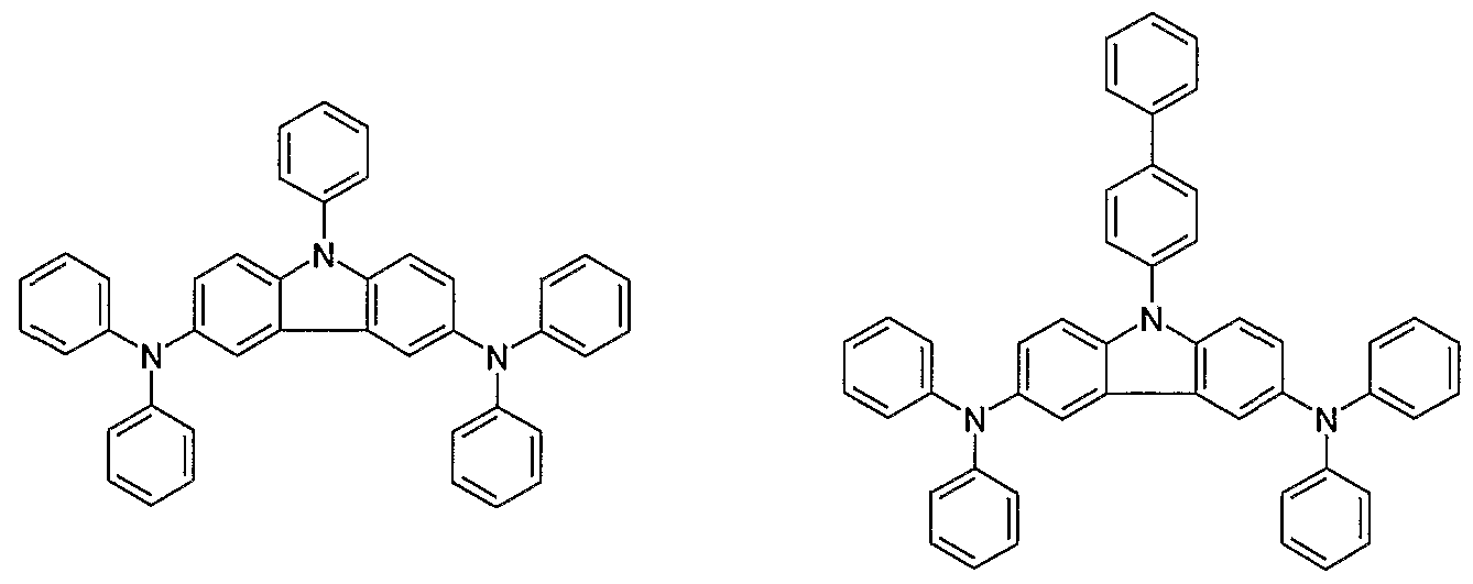


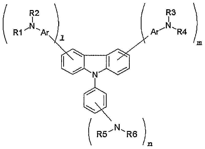

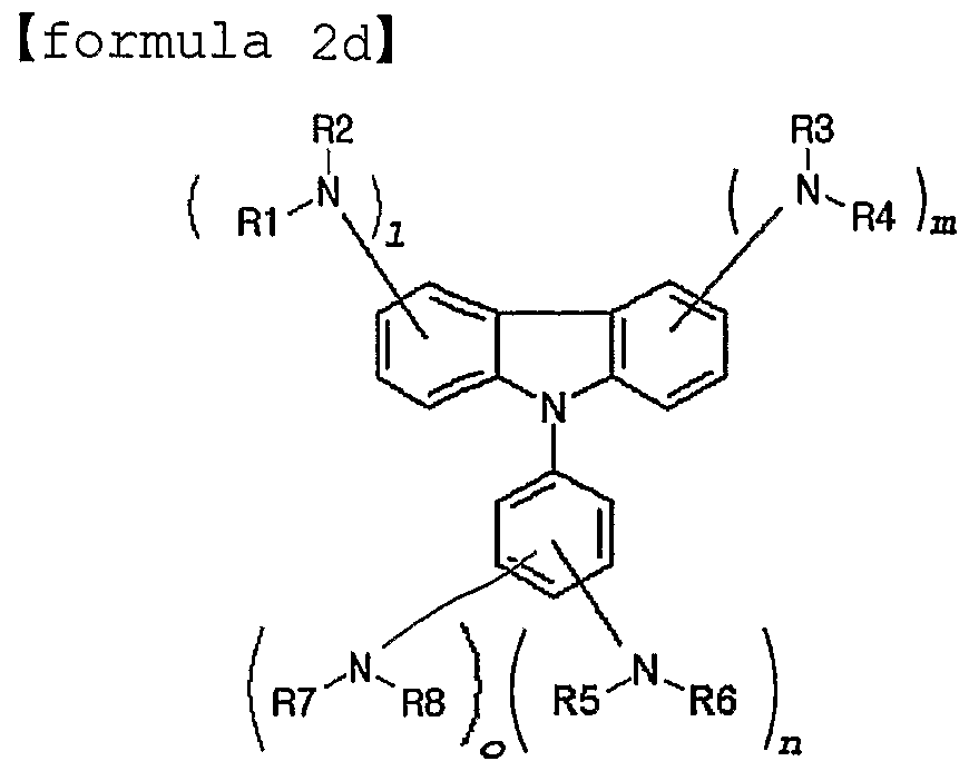

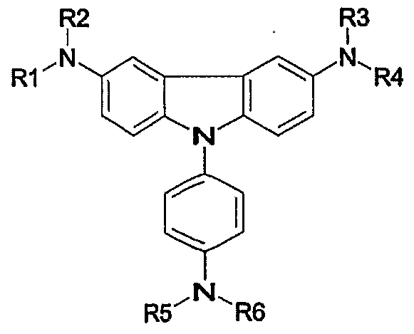


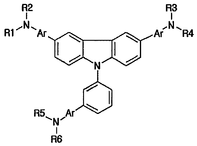


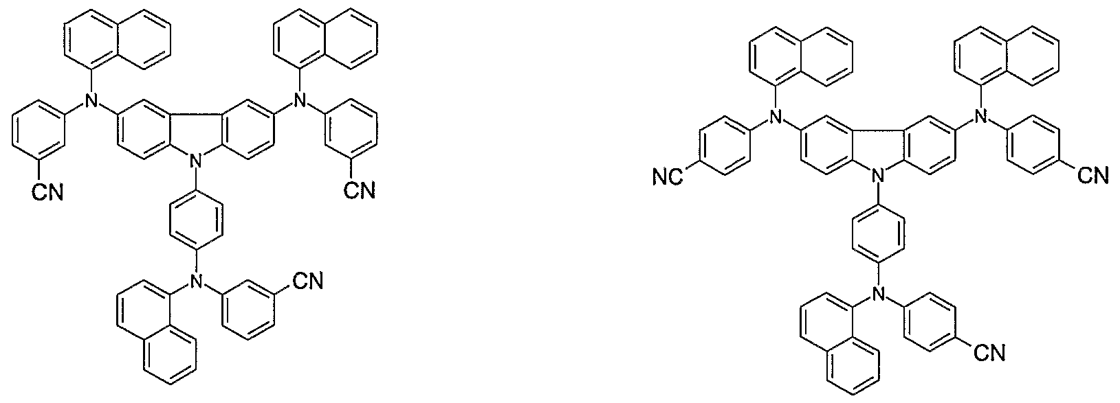


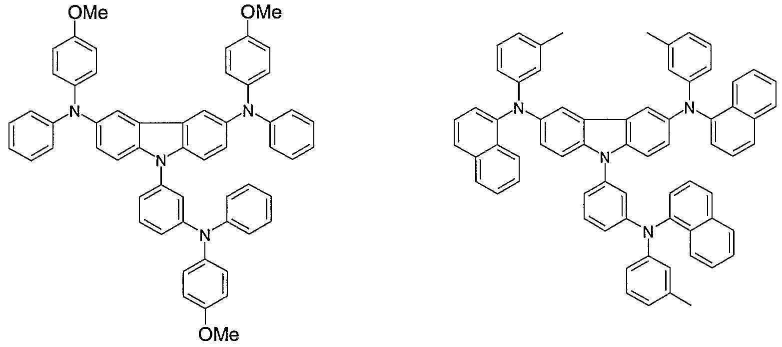


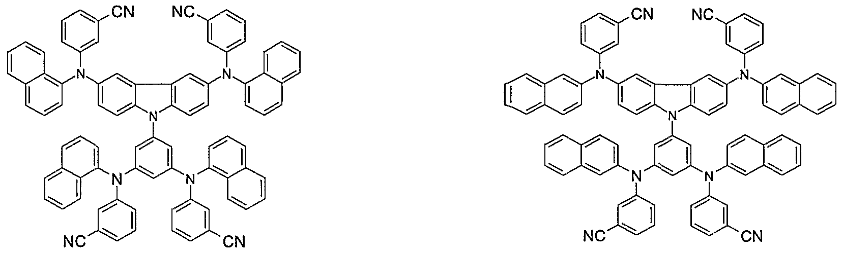


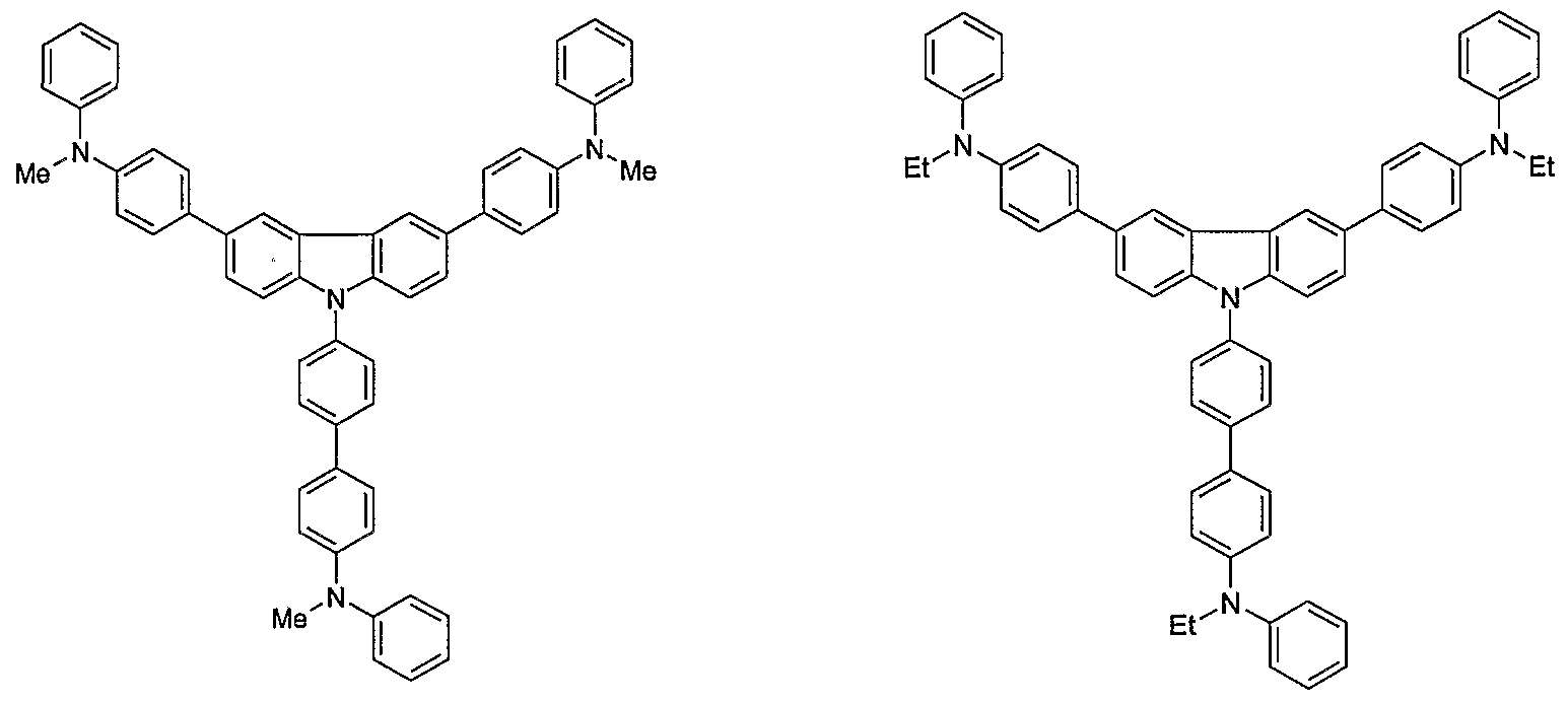


Claims


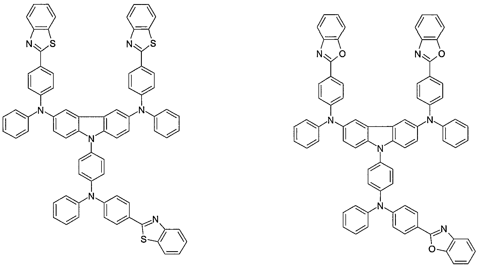


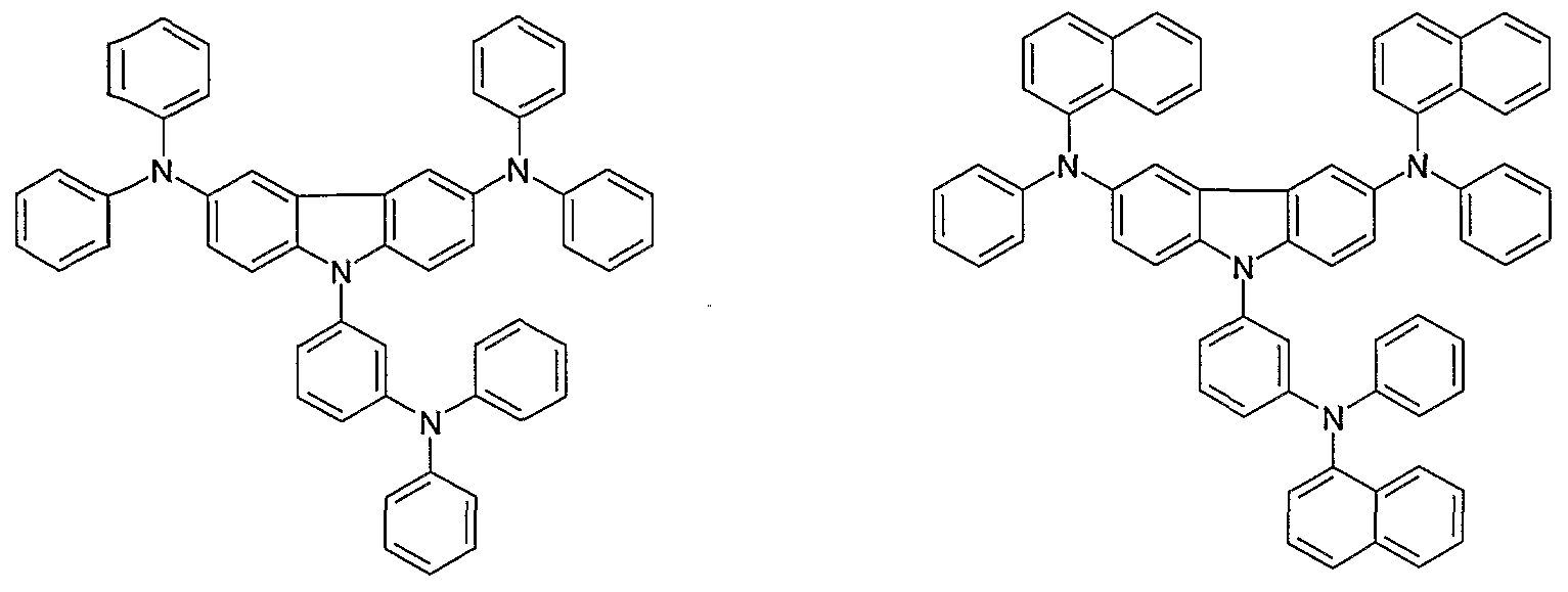


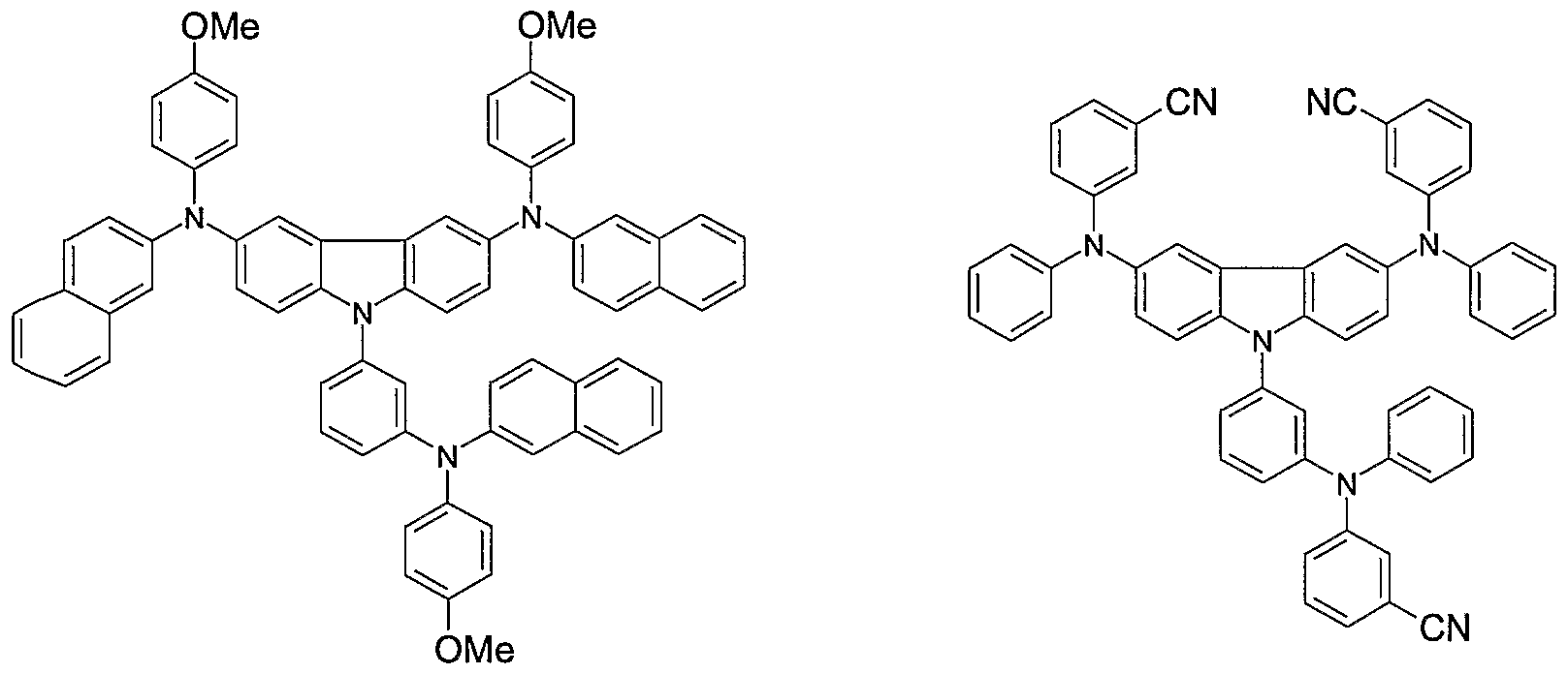


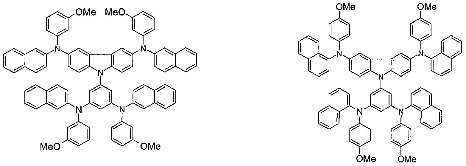


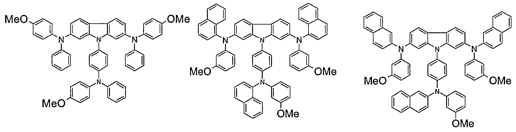


Priority Applications (2)
| Application Number | Priority Date | Filing Date | Title |
|---|---|---|---|
| JP2006546860A JP5242917B2 (en) | 2004-03-19 | 2005-03-18 | Novel hole injection or transport material and organic light emitting device using the same |
| EP05733437.7A EP1725632B1 (en) | 2004-03-19 | 2005-03-18 | Organic electroluminescence devices comprising new materials for injecting holes |
Applications Claiming Priority (4)
| Application Number | Priority Date | Filing Date | Title |
|---|---|---|---|
| KR10-2004-0018877 | 2004-03-19 | ||
| KR20040018877 | 2004-03-19 | ||
| KR1020040116388A KR20050118098A (en) | 2004-03-19 | 2004-12-30 | New materials for injecting or transporting holes and organic electroluminescence devices using the same |
| KR10-2004-0116388 | 2004-12-30 |
Publications (1)
| Publication Number | Publication Date |
|---|---|
| WO2005090512A1 true WO2005090512A1 (en) | 2005-09-29 |
Family
ID=34993679
Family Applications (1)
| Application Number | Title | Priority Date | Filing Date |
|---|---|---|---|
| PCT/KR2005/000794 WO2005090512A1 (en) | 2004-03-19 | 2005-03-18 | New materials for injecting or transporting holes and organic electroluminescence devices using the same |
Country Status (5)
| Country | Link |
|---|---|
| US (1) | US8198801B2 (en) |
| EP (1) | EP1725632B1 (en) |
| JP (1) | JP5242917B2 (en) |
| KR (1) | KR100664390B1 (en) |
| WO (1) | WO2005090512A1 (en) |
Cited By (31)
| Publication number | Priority date | Publication date | Assignee | Title |
|---|---|---|---|---|
| WO2006043647A1 (en) * | 2004-10-19 | 2006-04-27 | Semiconductor Energy Laboratory Co., Ltd. | Carbazole derivative, and light emitting element and light emitting device using the carbazole derivative |
| WO2007007885A1 (en) * | 2005-07-14 | 2007-01-18 | Semiconductor Energy Laboratory Co., Ltd. | Carbazole derivative, and light emitting element material, light emitting element, and electronic appliance obtained using the same |
| WO2007020804A1 (en) * | 2005-08-12 | 2007-02-22 | Semiconductor Energy Laboratory Co., Ltd. | Arylamine compound and synthetic method thereof |
| WO2008038607A1 (en) * | 2006-09-28 | 2008-04-03 | Semiconductor Energy Laboratory Co., Ltd. | Anthracene derivative, and light emitting element, light emitting device, and electronic device using the anthracene derivative |
| JP2008106063A (en) * | 2006-09-28 | 2008-05-08 | Semiconductor Energy Lab Co Ltd | Anthracene derivative, and light emitting element, light emitting apparatus and electronic equipment that employ anthracene derivative therein |
| WO2008062636A1 (en) * | 2006-11-24 | 2008-05-29 | Idemitsu Kosan Co., Ltd. | Aromatic amine derivative and organic electroluminescent element using the same |
| WO2008069756A1 (en) * | 2006-12-08 | 2008-06-12 | Agency For Science, Technology And Research | Arylamine compounds and electronic devices |
| WO2009061156A1 (en) * | 2007-11-08 | 2009-05-14 | Lg Chem, Ltd. | New compound and organic light emitting device using the same |
| WO2009061145A1 (en) * | 2007-11-08 | 2009-05-14 | Lg Chem, Ltd. | New compound and organic light emitting device using the same |
| WO2010021524A3 (en) * | 2008-08-22 | 2010-06-24 | 주식회사 엘지화학 | Material for organic electronic device, and organic electronic device using the same |
| CN101838262A (en) * | 2009-03-20 | 2010-09-22 | 株式会社半导体能源研究所 | Have the carbazole derivative of hetero-aromatic ring and use its luminous element and light-emitting device |
| US7879464B2 (en) | 2005-07-27 | 2011-02-01 | Semiconductor Energy Laboratory Co., Ltd. | Anthracene derivative, material for light emitting element, light emitting element, light emitting device, and electronic appliance |
| WO2011034967A1 (en) * | 2009-09-16 | 2011-03-24 | Nitto Denko Corporation | Compounds for organic light emitting diode emissive layers |
| EP2492260A1 (en) * | 2009-10-20 | 2012-08-29 | Tosoh Corporation | Carbazole compound and use thereof |
| EP1985613B1 (en) * | 2007-04-25 | 2013-05-15 | Semiconductor Energy Laboratory Co., Ltd. | Organic compound, anthracene derivative, and light-emitting element, light-emitting device, and electronic device in which the anthracene derivative is used |
| WO2013094951A1 (en) * | 2011-12-23 | 2013-06-27 | 제일모직 주식회사 | Compound for organic optoelectronic device, organic light-emitting diode containing same, and display device comprising organic light-emitting diode |
| US8617725B2 (en) | 2007-08-31 | 2013-12-31 | Semiconductor Energy Laboratory Co., Ltd. | Light-emitting element, light-emitting device, and electronic appliance |
| US8642782B2 (en) | 2010-09-21 | 2014-02-04 | Semiconductor Energy Laboratory Co., Ltd. | Carbazole derivative, light-emitting element material and organic semiconductor material |
| US8697885B2 (en) | 2010-11-30 | 2014-04-15 | Semiconductor Energy Laboratory Co., Ltd. | Carbazole compound, light-emitting element material, organic semiconductor material, light-emitting element, light emitting device, lighting device, and electronic device |
| US8808879B2 (en) | 2010-07-19 | 2014-08-19 | Nitto Denko Corporation | Phototherapy devices and methods comprising substituted carbazole compounds |
| US8853403B2 (en) | 2009-03-31 | 2014-10-07 | Semiconductor Energy Laboratory Co., Ltd. | Heterocyclic compound and light-emitting element, light-emitting device, lighting device, and electronic device using the same |
| EP2821460A1 (en) | 2012-02-27 | 2015-01-07 | LG Chem, Ltd. | Organic light emitting diode |
| US9142783B2 (en) | 2004-11-30 | 2015-09-22 | Semiconductor Energy Laboratory Co., Ltd. | Light emitting element and light emitting device |
| US9172045B2 (en) | 2011-10-26 | 2015-10-27 | Tosoh Corporation | 4-aminocarbazole compound and use thereof |
| FR3024144A1 (en) * | 2014-07-28 | 2016-01-29 | Univ Tours Francois Rabelais | NOVEL SYNTHONS FOR THE PRODUCTION OF ORGANIC SEMICONDUCTORS |
| KR20160073287A (en) | 2014-12-15 | 2016-06-24 | 삼성디스플레이 주식회사 | Carbazole compound, material for organic electroluminensence device, and organic electroluminescence device |
| WO2016116528A1 (en) * | 2015-01-20 | 2016-07-28 | Cynora Gmbh | Symmetrical organic molecules for use in optoelectronic components |
| US9412962B2 (en) | 2012-08-03 | 2016-08-09 | Semiconductor Energy Laboratory Co., Ltd. | Light-emitting element, light-emitting device, electronic device, and lighting device |
| US9525143B2 (en) | 2011-06-24 | 2016-12-20 | Semiconductor Energy Laboratory Co., Ltd. | Triarylamine compound, light-emitting element, light-emitting device, electronic device, and lighting device |
| US9732036B2 (en) | 2009-08-28 | 2017-08-15 | Hodogaya Chemical Co., Ltd. | Compound having carbazole ring structure, and organic electroluminescent device |
| US10556864B2 (en) | 2007-12-03 | 2020-02-11 | Semiconductor Energy Laboratory Co., Ltd. | Carbazole derivative, and light-emitting element, light-emitting device, and electronic device using the carbazole derivative |
Families Citing this family (20)
| Publication number | Priority date | Publication date | Assignee | Title |
|---|---|---|---|---|
| KR20050118098A (en) * | 2004-03-19 | 2005-12-15 | 주식회사 엘지화학 | New materials for injecting or transporting holes and organic electroluminescence devices using the same |
| JP4869690B2 (en) * | 2004-11-30 | 2012-02-08 | 株式会社半導体エネルギー研究所 | LIGHT EMITTING ELEMENT, LIGHT EMITTING DEVICE AND COMPOSITE MATERIAL |
| JP5270571B2 (en) * | 2007-11-22 | 2013-08-21 | 出光興産株式会社 | Organic EL device |
| KR101026173B1 (en) * | 2008-06-13 | 2011-04-05 | 덕산하이메탈(주) | Novel carbazole derivatives and organic electroluminescent device comprising same |
| TWI528862B (en) * | 2009-01-21 | 2016-04-01 | 半導體能源研究所股份有限公司 | Light-emitting element, light-emitting device, and electronic device |
| US8367222B2 (en) * | 2009-02-27 | 2013-02-05 | Idemitsu Kosan Co., Ltd. | Organic electroluminescent device |
| KR101588895B1 (en) * | 2009-08-06 | 2016-01-27 | 엘지디스플레이 주식회사 | Organic Light Emitting Diode Display Device |
| JP5716270B2 (en) * | 2009-10-20 | 2015-05-13 | 東ソー株式会社 | Carbazole compounds and uses thereof |
| JP5585044B2 (en) * | 2009-10-20 | 2014-09-10 | 東ソー株式会社 | Carbazole compounds and uses thereof |
| KR101333610B1 (en) | 2010-10-28 | 2013-11-27 | 엘지디스플레이 주식회사 | Phosphorescent material for Organic electroluminescent device |
| JP5927875B2 (en) * | 2010-12-20 | 2016-06-01 | 東ソー株式会社 | Amine compounds and uses thereof |
| WO2012161554A2 (en) | 2011-05-25 | 2012-11-29 | 주식회사 엘엠에스 | Novel compound and organic electronic device comprising the compound |
| WO2014021569A1 (en) * | 2012-08-01 | 2014-02-06 | Sk Chemicals Co., Ltd. | Compound for organic electroluminescent device and organic electroluminescent device including the same |
| JP6307686B2 (en) * | 2012-12-05 | 2018-04-11 | 三星ディスプレイ株式會社Samsung Display Co.,Ltd. | AMINE DERIVATIVE, ORGANIC LIGHT EMITTING MATERIAL AND ORGANIC ELECTROLUMINESCENT DEVICE USING THE SAME |
| WO2014088047A1 (en) * | 2012-12-05 | 2014-06-12 | 三星ディスプレイ株式▲会▼社 | Amine derivative, organic light-emitting material, and organic electroluminescence element using same |
| WO2014106524A2 (en) * | 2013-01-03 | 2014-07-10 | Merck Patent Gmbh | Materials for electronic devices |
| JP2016100364A (en) | 2014-11-18 | 2016-05-30 | 三星ディスプレイ株式會社Samsung Display Co.,Ltd. | Material for organic electroluminescent element and organic electroluminescent element using the same |
| WO2017052221A1 (en) | 2015-09-22 | 2017-03-30 | 주식회사 엘지화학 | Novel compound and organic light-emitting element comprising same |
| WO2018020571A1 (en) * | 2016-07-26 | 2018-02-01 | 日立化成株式会社 | Organic electronics material |
| WO2018021381A1 (en) * | 2016-07-26 | 2018-02-01 | 日立化成株式会社 | Organic electronic material |
Citations (4)
| Publication number | Priority date | Publication date | Assignee | Title |
|---|---|---|---|---|
| US5475213A (en) * | 1992-10-22 | 1995-12-12 | Mitsubishi Chemical Corporation | Optical information processing element and a light-to-light converting device |
| US6451455B1 (en) * | 1998-04-01 | 2002-09-17 | The Trustees Of Princeton University | Metal complexes bearing both electron transporting and hole transporting moieties |
| US6660410B2 (en) * | 2000-03-27 | 2003-12-09 | Idemitsu Kosan Co., Ltd. | Organic electroluminescence element |
| US6696181B2 (en) * | 2000-11-30 | 2004-02-24 | Hitachi, Ltd. | Organic-electroluminescence device, process for its production and organic-electroluminescence display system |
Family Cites Families (37)
| Publication number | Priority date | Publication date | Assignee | Title |
|---|---|---|---|---|
| US4356429A (en) | 1980-07-17 | 1982-10-26 | Eastman Kodak Company | Organic electroluminescent cell |
| US4539507A (en) | 1983-03-25 | 1985-09-03 | Eastman Kodak Company | Organic electroluminescent devices having improved power conversion efficiencies |
| US4769292A (en) * | 1987-03-02 | 1988-09-06 | Eastman Kodak Company | Electroluminescent device with modified thin film luminescent zone |
| JPH01245087A (en) | 1987-12-11 | 1989-09-29 | Idemitsu Kosan Co Ltd | Organic electroluminescence element |
| JPH02289675A (en) | 1989-01-13 | 1990-11-29 | Ricoh Co Ltd | Electric field light emitting element |
| JP2665788B2 (en) | 1989-01-17 | 1997-10-22 | 旭化成工業株式会社 | Organic electroluminescent device |
| JP2749407B2 (en) | 1989-02-20 | 1998-05-13 | パイオニア株式会社 | EL device |
| JP2731216B2 (en) | 1989-02-23 | 1998-03-25 | パイオニア株式会社 | EL device |
| JP2790353B2 (en) | 1989-03-15 | 1998-08-27 | 出光興産株式会社 | Organic thin-film electroluminescence device |
| WO1992005131A1 (en) * | 1990-09-20 | 1992-04-02 | Idemitsu Kosan Co., Ltd. | Organic electroluminescent element |
| JP3016896B2 (en) * | 1991-04-08 | 2000-03-06 | パイオニア株式会社 | Organic electroluminescence device |
| US5150006A (en) * | 1991-08-01 | 1992-09-22 | Eastman Kodak Company | Blue emitting internal junction organic electroluminescent device (II) |
| EP0569827A2 (en) * | 1992-05-11 | 1993-11-18 | Idemitsu Kosan Company Limited | Organic electroluminescence device |
| JP3071091B2 (en) | 1993-03-17 | 2000-07-31 | 三洋電機株式会社 | EL device |
| EP0676461B1 (en) * | 1994-04-07 | 2002-08-14 | Covion Organic Semiconductors GmbH | Spiro compounds and their application as electroluminescence materials |
| US5554459A (en) * | 1996-01-23 | 1996-09-10 | Bell Communications Research, Inc. | Material and method for low internal resistance LI-ion battery |
| JP3650218B2 (en) | 1996-05-10 | 2005-05-18 | ケミプロ化成株式会社 | High molecular weight aromatic amine compound and hole transporting material comprising the same |
| JP3649302B2 (en) * | 1996-05-23 | 2005-05-18 | 出光興産株式会社 | Organic electroluminescence device |
| US5645948A (en) * | 1996-08-20 | 1997-07-08 | Eastman Kodak Company | Blue organic electroluminescent devices |
| JP3709637B2 (en) * | 1996-12-16 | 2005-10-26 | 東洋インキ製造株式会社 | Hole transport material and use thereof |
| JP4088985B2 (en) | 1997-05-09 | 2008-05-21 | コニカミノルタホールディングス株式会社 | Organic electroluminescence device using new amino compound |
| JPH11345686A (en) | 1997-08-07 | 1999-12-14 | Fuji Photo Film Co Ltd | Organic electroluminescence element |
| JPH11219788A (en) | 1998-02-02 | 1999-08-10 | Casio Comput Co Ltd | Electroluminescence element |
| JP4081869B2 (en) * | 1998-08-17 | 2008-04-30 | コニカミノルタホールディングス株式会社 | Organic electroluminescence devices using new amino compounds |
| CN1213127C (en) * | 1998-09-09 | 2005-08-03 | 出光兴产株式会社 | Organic electroluminescent device and phenylenediamine derivative |
| CA2282988C (en) * | 1999-09-21 | 2006-06-20 | Royal Group Technologies Limited | Water resistant window frame |
| JP2002047271A (en) * | 2000-07-28 | 2002-02-12 | Jsr Corp | Carbazole derivative, carbazole-based polymer and hole- transporting material |
| JP2002124389A (en) * | 2000-10-16 | 2002-04-26 | Jsr Corp | Organic electroluminescent element |
| TWI297038B (en) * | 2000-11-22 | 2008-05-21 | Academia Sinica | 3,6,9-trisubstituted carbazoles for light emitting diodes |
| US6699597B2 (en) * | 2001-08-16 | 2004-03-02 | 3M Innovative Properties Company | Method and materials for patterning of an amorphous, non-polymeric, organic matrix with electrically active material disposed therein |
| JP2003075955A (en) * | 2001-09-03 | 2003-03-12 | Konica Corp | Photothermographic imaging material with improved silver tone |
| DE10203328A1 (en) * | 2002-01-28 | 2003-08-07 | Syntec Ges Fuer Chemie Und Tec | New triarylamine derivatives with space-filling wing groups and their use in electro-photographic and organic electroluminescent devices |
| JP2003238501A (en) | 2002-02-18 | 2003-08-27 | Idemitsu Kosan Co Ltd | Aromatic oligoamine derivative and organic electroluminescent element containing the same |
| US20030205696A1 (en) | 2002-04-25 | 2003-11-06 | Canon Kabushiki Kaisha | Carbazole-based materials for guest-host electroluminescent systems |
| US20040001969A1 (en) * | 2002-06-27 | 2004-01-01 | Eastman Kodak Company | Device containing green organic light-emitting diode |
| KR100515516B1 (en) * | 2002-11-30 | 2005-09-16 | 신동명 | Organic light emitting materials and Organic electroluminescence devices using the same |
| EP1805140B1 (en) * | 2004-10-19 | 2016-08-31 | Semiconductor Energy Laboratory Co., Ltd. | Carbazole derivative, and light emitting element and light emitting device using the carbazole derivative |
-
2005
- 2005-03-18 EP EP05733437.7A patent/EP1725632B1/en active Active
- 2005-03-18 US US11/083,360 patent/US8198801B2/en active Active
- 2005-03-18 KR KR1020050022762A patent/KR100664390B1/en active IP Right Grant
- 2005-03-18 WO PCT/KR2005/000794 patent/WO2005090512A1/en not_active Application Discontinuation
- 2005-03-18 JP JP2006546860A patent/JP5242917B2/en active Active
Patent Citations (4)
| Publication number | Priority date | Publication date | Assignee | Title |
|---|---|---|---|---|
| US5475213A (en) * | 1992-10-22 | 1995-12-12 | Mitsubishi Chemical Corporation | Optical information processing element and a light-to-light converting device |
| US6451455B1 (en) * | 1998-04-01 | 2002-09-17 | The Trustees Of Princeton University | Metal complexes bearing both electron transporting and hole transporting moieties |
| US6660410B2 (en) * | 2000-03-27 | 2003-12-09 | Idemitsu Kosan Co., Ltd. | Organic electroluminescence element |
| US6696181B2 (en) * | 2000-11-30 | 2004-02-24 | Hitachi, Ltd. | Organic-electroluminescence device, process for its production and organic-electroluminescence display system |
Non-Patent Citations (1)
| Title |
|---|
| See also references of EP1725632A4 * |
Cited By (69)
| Publication number | Priority date | Publication date | Assignee | Title |
|---|---|---|---|---|
| WO2006043647A1 (en) * | 2004-10-19 | 2006-04-27 | Semiconductor Energy Laboratory Co., Ltd. | Carbazole derivative, and light emitting element and light emitting device using the carbazole derivative |
| US8900728B2 (en) | 2004-10-19 | 2014-12-02 | Semiconductor Energy Laboratory Co., Ltd. | Carbazole derivative, and light emitting element and light emitting device using the carbazole derivative |
| US8431248B2 (en) | 2004-10-19 | 2013-04-30 | Semiconductor Energy Laboratory Co., Ltd. | Carbazole derivative, and light emitting element and light emitting device using the carbazole derivative |
| US7901791B2 (en) | 2004-10-19 | 2011-03-08 | Semiconductor Energy Laboratory Co., Ltd. | Carbazole derivative, and light emitting element and light emitting device using the carbazole derivative |
| US9142783B2 (en) | 2004-11-30 | 2015-09-22 | Semiconductor Energy Laboratory Co., Ltd. | Light emitting element and light emitting device |
| JP2009246396A (en) * | 2005-07-14 | 2009-10-22 | Semiconductor Energy Lab Co Ltd | Light emitting element and light emitting device |
| WO2007007885A1 (en) * | 2005-07-14 | 2007-01-18 | Semiconductor Energy Laboratory Co., Ltd. | Carbazole derivative, and light emitting element material, light emitting element, and electronic appliance obtained using the same |
| US7838128B2 (en) | 2005-07-14 | 2010-11-23 | Semiconductor Energy Laboratory Co., Ltd. | Carbazole derivative, and light emitting element material, light emitting element, and electronic appliance obtained using the same |
| US7879464B2 (en) | 2005-07-27 | 2011-02-01 | Semiconductor Energy Laboratory Co., Ltd. | Anthracene derivative, material for light emitting element, light emitting element, light emitting device, and electronic appliance |
| WO2007020804A1 (en) * | 2005-08-12 | 2007-02-22 | Semiconductor Energy Laboratory Co., Ltd. | Arylamine compound and synthetic method thereof |
| EP2066629A1 (en) * | 2006-09-28 | 2009-06-10 | Semiconductor Energy Laboratory Co, Ltd. | Anthracene derivative, and light emitting element, light emitting device, and electronic device using the anthracene derivative |
| WO2008038607A1 (en) * | 2006-09-28 | 2008-04-03 | Semiconductor Energy Laboratory Co., Ltd. | Anthracene derivative, and light emitting element, light emitting device, and electronic device using the anthracene derivative |
| JP2008106063A (en) * | 2006-09-28 | 2008-05-08 | Semiconductor Energy Lab Co Ltd | Anthracene derivative, and light emitting element, light emitting apparatus and electronic equipment that employ anthracene derivative therein |
| EP2066629A4 (en) * | 2006-09-28 | 2010-12-22 | Semiconductor Energy Lab | Anthracene derivative, and light emitting element, light emitting device, and electronic device using the anthracene derivative |
| US7880019B2 (en) | 2006-09-28 | 2011-02-01 | Semiconductor Energy Laboratory Co., Ltd. | Anthracene derivative, and light emitting element, light emitting device, and electronic device using the anthracene derivative |
| US8546792B2 (en) | 2006-09-28 | 2013-10-01 | Semiconductor Energy Laboratory Co., Ltd. | Anthracene derivative, and light emitting element, light emitting device, and electronic device using the anthracene derivative |
| US8394510B2 (en) | 2006-11-24 | 2013-03-12 | Idemitsu Kosan Co., Ltd. | Aromatic amine derivative and organic electroluminescence device using the same |
| US8895159B2 (en) | 2006-11-24 | 2014-11-25 | Idemitsu Kosan Co., Ltd. | Aromatic amine derivative and organic electroluminescence device using the same |
| EP2085382A1 (en) | 2006-11-24 | 2009-08-05 | Idemitsu Kosan Co., Ltd. | Aromatic amine derivative and organic electroluminescent element using the same |
| WO2008062636A1 (en) * | 2006-11-24 | 2008-05-29 | Idemitsu Kosan Co., Ltd. | Aromatic amine derivative and organic electroluminescent element using the same |
| JP5133259B2 (en) * | 2006-11-24 | 2013-01-30 | 出光興産株式会社 | Aromatic amine derivative and organic electroluminescence device using the same |
| WO2008069756A1 (en) * | 2006-12-08 | 2008-06-12 | Agency For Science, Technology And Research | Arylamine compounds and electronic devices |
| US8518559B2 (en) | 2006-12-08 | 2013-08-27 | Agency For Science, Technology And Research | Arylamine compounds and electronic devices |
| JP2019163272A (en) * | 2007-04-25 | 2019-09-26 | 株式会社半導体エネルギー研究所 | Method for synthesizing organic compound |
| EP1985613B1 (en) * | 2007-04-25 | 2013-05-15 | Semiconductor Energy Laboratory Co., Ltd. | Organic compound, anthracene derivative, and light-emitting element, light-emitting device, and electronic device in which the anthracene derivative is used |
| US11171292B2 (en) | 2007-04-25 | 2021-11-09 | Semiconductor Energy Laboratory Co., Ltd. | Organic compound, anthracene derivative, and light-emitting element, light-emitting device, and electronic device in which the anthracene derivative is used |
| US8835018B2 (en) | 2007-04-25 | 2014-09-16 | Semiconductor Energy Laboratory Co., Ltd. | Organic compound, anthracene derivative, and light-emitting element, light-emitting device, and electronic device in which the anthracene derivative is used |
| US9831440B2 (en) | 2007-04-25 | 2017-11-28 | Semiconductor Energy Laboratory Co., Ltd. | Organic compound, anthracene derivative, and light-emitting element, light-emitting device, and electronic device in which the anthracene derivative is used |
| US9461248B2 (en) | 2007-04-25 | 2016-10-04 | Semiconductor Energy Laboratory Co., Ltd. | Organic compound, anthracene derivative, and light-emitting element, light-emitting device, and electronic device in which the anthracene derivative is used |
| US8617725B2 (en) | 2007-08-31 | 2013-12-31 | Semiconductor Energy Laboratory Co., Ltd. | Light-emitting element, light-emitting device, and electronic appliance |
| US8395143B2 (en) | 2007-11-08 | 2013-03-12 | Lg Chem, Ltd. | Compound and organic light emitting device using the same |
| US8968884B2 (en) | 2007-11-08 | 2015-03-03 | Lg Chem, Ltd. | Compound and organic light emitting device using the same |
| US20110127495A1 (en) * | 2007-11-08 | 2011-06-02 | Sung-Kil Hong | New compound and organic light emitting device using the same |
| WO2009061156A1 (en) * | 2007-11-08 | 2009-05-14 | Lg Chem, Ltd. | New compound and organic light emitting device using the same |
| WO2009061145A1 (en) * | 2007-11-08 | 2009-05-14 | Lg Chem, Ltd. | New compound and organic light emitting device using the same |
| US10556864B2 (en) | 2007-12-03 | 2020-02-11 | Semiconductor Energy Laboratory Co., Ltd. | Carbazole derivative, and light-emitting element, light-emitting device, and electronic device using the carbazole derivative |
| WO2010021524A3 (en) * | 2008-08-22 | 2010-06-24 | 주식회사 엘지화학 | Material for organic electronic device, and organic electronic device using the same |
| US9722188B2 (en) | 2008-08-22 | 2017-08-01 | Lg Chem, Ltd. | Material for organic electronic device, and organic electronic device using the same |
| US9196845B2 (en) | 2008-08-22 | 2015-11-24 | Lg Chem, Ltd. | Material for organic electronic device, and organic electronic device using same |
| US9190618B2 (en) | 2008-08-22 | 2015-11-17 | Lg Chem, Ltd. | Material for organic electronic device, and organic electronic device using same |
| CN101838262A (en) * | 2009-03-20 | 2010-09-22 | 株式会社半导体能源研究所 | Have the carbazole derivative of hetero-aromatic ring and use its luminous element and light-emitting device |
| US8530658B2 (en) | 2009-03-20 | 2013-09-10 | Semiconductor Energy Laboratory Co., Ltd. | Carbazole derivative with heteroaromatic ring, and light-emitting element, light-emitting device, and electronic device using carbazole derivative with heteroaromatic ring |
| US8853403B2 (en) | 2009-03-31 | 2014-10-07 | Semiconductor Energy Laboratory Co., Ltd. | Heterocyclic compound and light-emitting element, light-emitting device, lighting device, and electronic device using the same |
| US9732036B2 (en) | 2009-08-28 | 2017-08-15 | Hodogaya Chemical Co., Ltd. | Compound having carbazole ring structure, and organic electroluminescent device |
| US8586205B2 (en) | 2009-09-16 | 2013-11-19 | Nitto Denko Corporation | Compounds for organic light emitting diode emissive layers |
| WO2011034967A1 (en) * | 2009-09-16 | 2011-03-24 | Nitto Denko Corporation | Compounds for organic light emitting diode emissive layers |
| EP2492260A1 (en) * | 2009-10-20 | 2012-08-29 | Tosoh Corporation | Carbazole compound and use thereof |
| EP2492260A4 (en) * | 2009-10-20 | 2014-08-27 | Tosoh Corp | Carbazole compound and use thereof |
| US9650565B2 (en) | 2009-10-20 | 2017-05-16 | Tosoh Corporation | Carbazole compound and use thereof |
| US8808879B2 (en) | 2010-07-19 | 2014-08-19 | Nitto Denko Corporation | Phototherapy devices and methods comprising substituted carbazole compounds |
| US8642782B2 (en) | 2010-09-21 | 2014-02-04 | Semiconductor Energy Laboratory Co., Ltd. | Carbazole derivative, light-emitting element material and organic semiconductor material |
| US9450188B2 (en) | 2010-09-21 | 2016-09-20 | Semiconductor Energy Laboratory Co., Ltd. | Carbazole derivative, light-emitting element material and organic semiconductor material |
| US10071993B2 (en) | 2010-09-21 | 2018-09-11 | Semiconductor Energy Laboratory Co., Ltd. | Carbazole derivative, light-emitting element material and organic semiconductor material |
| US8697885B2 (en) | 2010-11-30 | 2014-04-15 | Semiconductor Energy Laboratory Co., Ltd. | Carbazole compound, light-emitting element material, organic semiconductor material, light-emitting element, light emitting device, lighting device, and electronic device |
| US9525143B2 (en) | 2011-06-24 | 2016-12-20 | Semiconductor Energy Laboratory Co., Ltd. | Triarylamine compound, light-emitting element, light-emitting device, electronic device, and lighting device |
| US9172045B2 (en) | 2011-10-26 | 2015-10-27 | Tosoh Corporation | 4-aminocarbazole compound and use thereof |
| WO2013094951A1 (en) * | 2011-12-23 | 2013-06-27 | 제일모직 주식회사 | Compound for organic optoelectronic device, organic light-emitting diode containing same, and display device comprising organic light-emitting diode |
| US9331287B2 (en) | 2012-02-27 | 2016-05-03 | Lg Chem, Ltd. | Organic light emitting diode |
| EP2821460A1 (en) | 2012-02-27 | 2015-01-07 | LG Chem, Ltd. | Organic light emitting diode |
| US11043637B2 (en) | 2012-08-03 | 2021-06-22 | Semiconductor Energy Laboratory Co., Ltd. | Light-emitting element, light-emitting device, electronic device, and lighting device |
| US11968889B2 (en) | 2012-08-03 | 2024-04-23 | Semiconductor Energy Laboratory Co., Ltd. | Light-emitting element, light-emitting device, electronic device, and lighting device |
| US10069076B2 (en) | 2012-08-03 | 2018-09-04 | Semiconductor Energy Laboratory Co., Ltd. | Light-emitting element, light-emitting device, electronic device, and lighting device |
| US9412962B2 (en) | 2012-08-03 | 2016-08-09 | Semiconductor Energy Laboratory Co., Ltd. | Light-emitting element, light-emitting device, electronic device, and lighting device |
| US10897012B2 (en) | 2012-08-03 | 2021-01-19 | Semiconductor Energy Laboratory Co., Ltd. | Light-emitting element, light-emitting device, electronic device, and lighting device |
| WO2016016221A1 (en) * | 2014-07-28 | 2016-02-04 | Universite De Tours Francois-Rabelais | Novel synthons for developing organic semiconductors |
| FR3024144A1 (en) * | 2014-07-28 | 2016-01-29 | Univ Tours Francois Rabelais | NOVEL SYNTHONS FOR THE PRODUCTION OF ORGANIC SEMICONDUCTORS |
| US10084142B2 (en) | 2014-12-15 | 2018-09-25 | Samsung Display Co., Ltd. | Carbazole compound, material for organic electroluminescent device, and organic electroluminescent device |
| KR20160073287A (en) | 2014-12-15 | 2016-06-24 | 삼성디스플레이 주식회사 | Carbazole compound, material for organic electroluminensence device, and organic electroluminescence device |
| WO2016116528A1 (en) * | 2015-01-20 | 2016-07-28 | Cynora Gmbh | Symmetrical organic molecules for use in optoelectronic components |
Also Published As
| Publication number | Publication date |
|---|---|
| EP1725632B1 (en) | 2014-04-30 |
| KR100664390B1 (en) | 2007-01-02 |
| EP1725632A1 (en) | 2006-11-29 |
| JP5242917B2 (en) | 2013-07-24 |
| EP1725632A4 (en) | 2009-05-06 |
| JP2007520470A (en) | 2007-07-26 |
| US20050225235A1 (en) | 2005-10-13 |
| KR20060044424A (en) | 2006-05-16 |
| US8198801B2 (en) | 2012-06-12 |
Similar Documents
| Publication | Publication Date | Title |
|---|---|---|
| EP1725632B1 (en) | Organic electroluminescence devices comprising new materials for injecting holes | |
| JP5566898B2 (en) | New organic light emitting device compound and organic light emitting device using the same | |
| EP2471771B1 (en) | Compound having carbazole ring structure and organic electroluminescent device | |
| EP2492986B1 (en) | Organic electroluminescent element | |
| JP5372867B2 (en) | Novel organic compound and organic light emitting device using the same | |
| EP2385052B1 (en) | Compound having oxadiazole ring structure substituted with pyridyl group, and organic electroluminescent device | |
| TWI294454B (en) | New material for injecting or transporting holes and organic electroluminescence devices using the same | |
| EP2388842B1 (en) | Organic electroluminescent element | |
| JP5175099B2 (en) | Compound having triazole ring structure substituted with pyridyl group and organic electroluminescence device | |
| US8173273B2 (en) | Anthracene derivatives, method for preparation thereof, and organic electronic device using the same | |
| JP5751727B2 (en) | Compound having pyridoindole ring structure in which substituted pyridyl group is linked and organic electroluminescence device | |
| JP2013539205A (en) | Novel organic electroluminescent compound and organic electroluminescent device using the same | |
| JPWO2008023628A1 (en) | Compound having triazine ring structure substituted with pyridyl group and organic electroluminescence device | |
| EP2463287B1 (en) | Compound having substituted anthracene ring structure and pyridoindole ring structure and organic electroluminescence device | |
| WO2009096549A1 (en) | Compound having substituted pyridyl group and pyridoindole ring structure linked through phenylene group, and organic electroluminescent device | |
| WO2010084729A1 (en) | Compound having triazole ring structure with pyridyl group attached thereto, and organic electroluminescent element | |
| JP2013542176A (en) | Novel compounds for organic electronic materials and organic electroluminescent devices using the same | |
| US8449989B2 (en) | Organic compound and organic light emitting device using the same | |
| JP2012056953A (en) | Compound having oxadiazole ring structure substituted with pyridyl group and organic electroluminescent device | |
| KR20030087522A (en) | A new material for organic luminescence layer and organic electroluminescent display using the same |
Legal Events
| Date | Code | Title | Description |
|---|---|---|---|
| WWE | Wipo information: entry into national phase |
Ref document number: 200580001667.2 Country of ref document: CN |
|
| AK | Designated states |
Kind code of ref document: A1 Designated state(s): AE AG AL AM AT AU AZ BA BB BG BR BW BY BZ CA CH CN CO CR CU CZ DE DK DM DZ EC EE EG ES FI GB GD GE GH GM HR HU ID IL IN IS JP KE KG KP KZ LC LK LR LS LT LU LV MA MD MG MK MN MW MX MZ NA NI NO NZ OM PG PH PL PT RO RU SC SD SE SG SK SL SM SY TJ TM TN TR TT TZ UA UG UZ VC VN YU ZA ZM ZW |
|
| AL | Designated countries for regional patents |
Kind code of ref document: A1 Designated state(s): GM KE LS MW MZ NA SD SL SZ TZ UG ZM ZW AM AZ BY KG KZ MD RU TJ TM AT BE BG CH CY CZ DE DK EE ES FI FR GB GR HU IE IS IT LT LU MC NL PL PT RO SE SI SK TR BF BJ CF CG CI CM GA GN GQ GW ML MR NE SN TD TG |
|
| 121 | Ep: the epo has been informed by wipo that ep was designated in this application | ||
| WWE | Wipo information: entry into national phase |
Ref document number: 2005733437 Country of ref document: EP |
|
| WWE | Wipo information: entry into national phase |
Ref document number: 1638/KOLNP/2006 Country of ref document: IN |
|
| WWE | Wipo information: entry into national phase |
Ref document number: 2006546860 Country of ref document: JP |
|
| NENP | Non-entry into the national phase |
Ref country code: DE |
|
| WWW | Wipo information: withdrawn in national office |
Ref document number: DE |
|
| WWP | Wipo information: published in national office |
Ref document number: 2005733437 Country of ref document: EP |