WO2006043647A1 - Carbazole derivative, and light emitting element and light emitting device using the carbazole derivative - Google Patents
Carbazole derivative, and light emitting element and light emitting device using the carbazole derivative Download PDFInfo
- Publication number
- WO2006043647A1 WO2006043647A1 PCT/JP2005/019349 JP2005019349W WO2006043647A1 WO 2006043647 A1 WO2006043647 A1 WO 2006043647A1 JP 2005019349 W JP2005019349 W JP 2005019349W WO 2006043647 A1 WO2006043647 A1 WO 2006043647A1
- Authority
- WO
- WIPO (PCT)
- Prior art keywords
- group
- light emitting
- carbon atoms
- emitting element
- carbazole derivative
- Prior art date
Links
- 0 Cc1ccc(*(**)c2ccc(*(*)c3ccc(*(c4ccccc4)c4ccccc4)cc3)cc2-2)c-2c1 Chemical compound Cc1ccc(*(**)c2ccc(*(*)c3ccc(*(c4ccccc4)c4ccccc4)cc3)cc2-2)c-2c1 0.000 description 4
- OWWIYWXGIMMYPA-UHFFFAOYSA-N C1C=CC(N(C(C2)C=Cc3c2c2cc(N(c4ccccc4)c4cccc(-c5nc(N(c6ccccc6)c6ccccc6)ccc5)n4)ccc2[n]3-c2ccccc2)c2cccc(C(N3)=CC=CC3N(c3ccccc3)C3=CCCC=C3)n2)=CC1 Chemical compound C1C=CC(N(C(C2)C=Cc3c2c2cc(N(c4ccccc4)c4cccc(-c5nc(N(c6ccccc6)c6ccccc6)ccc5)n4)ccc2[n]3-c2ccccc2)c2cccc(C(N3)=CC=CC3N(c3ccccc3)C3=CCCC=C3)n2)=CC1 OWWIYWXGIMMYPA-UHFFFAOYSA-N 0.000 description 1
- USOKJURYNOPMMQ-UHFFFAOYSA-N CC(C)(C)C(CC1)=Cc(c2cc(N(c(cc3)ccc3N(c3ccccc3)c3ccccc3)c3cccc4c3nccc4)ccc22)c1[n]2-c1ccccc1 Chemical compound CC(C)(C)C(CC1)=Cc(c2cc(N(c(cc3)ccc3N(c3ccccc3)c3ccccc3)c3cccc4c3nccc4)ccc22)c1[n]2-c1ccccc1 USOKJURYNOPMMQ-UHFFFAOYSA-N 0.000 description 1
- YKJOVIGIFINPIN-UHFFFAOYSA-N CC(C)(C)c(cc1c2cc(N(C3SC(N(c4ccccc4)c4ccccc4)=CN3)c3ccccc3)ccc22)ccc1[n]2-c1ccccc1 Chemical compound CC(C)(C)c(cc1c2cc(N(C3SC(N(c4ccccc4)c4ccccc4)=CN3)c3ccccc3)ccc22)ccc1[n]2-c1ccccc1 YKJOVIGIFINPIN-UHFFFAOYSA-N 0.000 description 1
- UVOYCOHETVAJKO-UHFFFAOYSA-N CC(C)(C)c(cc1c2cc(N(c3ccccc3)c(cc3)ccc3N(c3ccccc3)c3ccccc3)ccc22)ccc1[n]2-c(cc1)ccc1-c1ccccc1 Chemical compound CC(C)(C)c(cc1c2cc(N(c3ccccc3)c(cc3)ccc3N(c3ccccc3)c3ccccc3)ccc22)ccc1[n]2-c(cc1)ccc1-c1ccccc1 UVOYCOHETVAJKO-UHFFFAOYSA-N 0.000 description 1
- QLZPLOQCYYMQNN-UHFFFAOYSA-N CC(CC(N(C1SC(N(c2ccccc2)c2ccccc2)=CN1)c1ccccc1)=C1)c2c1c(cc(cc1)N(C3SC(N(c4ccccc4)c4ccccc4)=NC3)c3ccccc3)c1[n]2-c1ccccc1 Chemical compound CC(CC(N(C1SC(N(c2ccccc2)c2ccccc2)=CN1)c1ccccc1)=C1)c2c1c(cc(cc1)N(C3SC(N(c4ccccc4)c4ccccc4)=NC3)c3ccccc3)c1[n]2-c1ccccc1 QLZPLOQCYYMQNN-UHFFFAOYSA-N 0.000 description 1
- ZFUBWYFCPOWDCN-UHFFFAOYSA-N Cc1ccc(-c2ccc(C)[nH]2)[nH]1 Chemical compound Cc1ccc(-c2ccc(C)[nH]2)[nH]1 ZFUBWYFCPOWDCN-UHFFFAOYSA-N 0.000 description 1
- DPECCMXOGAHFKQ-UHFFFAOYSA-N c(cc1)ccc1N(c1ccccc1)c(cc1)ccc1N(c(cc1c2c3ccc(N(c(cc4)ccc4N(c4ccccc4)c4ccccc4)c4cccc5c4cccc5)c2)ccc1[n]3-c1ccccc1)c1c(cccc2)c2ccc1 Chemical compound c(cc1)ccc1N(c1ccccc1)c(cc1)ccc1N(c(cc1c2c3ccc(N(c(cc4)ccc4N(c4ccccc4)c4ccccc4)c4cccc5c4cccc5)c2)ccc1[n]3-c1ccccc1)c1c(cccc2)c2ccc1 DPECCMXOGAHFKQ-UHFFFAOYSA-N 0.000 description 1
- QXPAPGDQRWESTP-UHFFFAOYSA-N c(cc1)ccc1N(c1ccccc1)c(cc1)ccc1N(c1ccccc1)c(cc1c2c3cccc2)ccc1[n]3-c1ccccc1 Chemical compound c(cc1)ccc1N(c1ccccc1)c(cc1)ccc1N(c1ccccc1)c(cc1c2c3cccc2)ccc1[n]3-c1ccccc1 QXPAPGDQRWESTP-UHFFFAOYSA-N 0.000 description 1
- QIEWTACDLJLBTE-UHFFFAOYSA-N c(cc1)ccc1N(c1ccccc1)c(cc1)ccc1N(c1ccccc1)c(cc1c2cc(N(c3ccccc3)c(cc3)ccc3N(c3ccccc3)c3ccccc3)ccc22)ccc1[n]2-c1ccccc1 Chemical compound c(cc1)ccc1N(c1ccccc1)c(cc1)ccc1N(c1ccccc1)c(cc1c2cc(N(c3ccccc3)c(cc3)ccc3N(c3ccccc3)c3ccccc3)ccc22)ccc1[n]2-c1ccccc1 QIEWTACDLJLBTE-UHFFFAOYSA-N 0.000 description 1
- OCQFHFNWMCLWKC-UHFFFAOYSA-N c(cc1)ccc1Nc(cc1)ccc1N(c1ccccc1)c1ccccc1 Chemical compound c(cc1)ccc1Nc(cc1)ccc1N(c1ccccc1)c1ccccc1 OCQFHFNWMCLWKC-UHFFFAOYSA-N 0.000 description 1
Classifications
-
- H—ELECTRICITY
- H10—SEMICONDUCTOR DEVICES; ELECTRIC SOLID-STATE DEVICES NOT OTHERWISE PROVIDED FOR
- H10K—ORGANIC ELECTRIC SOLID-STATE DEVICES
- H10K85/00—Organic materials used in the body or electrodes of devices covered by this subclass
- H10K85/60—Organic compounds having low molecular weight
- H10K85/649—Aromatic compounds comprising a hetero atom
- H10K85/657—Polycyclic condensed heteroaromatic hydrocarbons
- H10K85/6572—Polycyclic condensed heteroaromatic hydrocarbons comprising only nitrogen in the heteroaromatic polycondensed ring system, e.g. phenanthroline or carbazole
-
- C—CHEMISTRY; METALLURGY
- C07—ORGANIC CHEMISTRY
- C07D—HETEROCYCLIC COMPOUNDS
- C07D209/00—Heterocyclic compounds containing five-membered rings, condensed with other rings, with one nitrogen atom as the only ring hetero atom
- C07D209/56—Ring systems containing three or more rings
- C07D209/80—[b, c]- or [b, d]-condensed
- C07D209/82—Carbazoles; Hydrogenated carbazoles
- C07D209/88—Carbazoles; Hydrogenated carbazoles with hetero atoms or with carbon atoms having three bonds to hetero atoms with at the most one bond to halogen, e.g. ester or nitrile radicals, directly attached to carbon atoms of the ring system
-
- C—CHEMISTRY; METALLURGY
- C07—ORGANIC CHEMISTRY
- C07D—HETEROCYCLIC COMPOUNDS
- C07D401/00—Heterocyclic compounds containing two or more hetero rings, having nitrogen atoms as the only ring hetero atoms, at least one ring being a six-membered ring with only one nitrogen atom
- C07D401/02—Heterocyclic compounds containing two or more hetero rings, having nitrogen atoms as the only ring hetero atoms, at least one ring being a six-membered ring with only one nitrogen atom containing two hetero rings
- C07D401/12—Heterocyclic compounds containing two or more hetero rings, having nitrogen atoms as the only ring hetero atoms, at least one ring being a six-membered ring with only one nitrogen atom containing two hetero rings linked by a chain containing hetero atoms as chain links
-
- C—CHEMISTRY; METALLURGY
- C07—ORGANIC CHEMISTRY
- C07D—HETEROCYCLIC COMPOUNDS
- C07D401/00—Heterocyclic compounds containing two or more hetero rings, having nitrogen atoms as the only ring hetero atoms, at least one ring being a six-membered ring with only one nitrogen atom
- C07D401/14—Heterocyclic compounds containing two or more hetero rings, having nitrogen atoms as the only ring hetero atoms, at least one ring being a six-membered ring with only one nitrogen atom containing three or more hetero rings
-
- C—CHEMISTRY; METALLURGY
- C07—ORGANIC CHEMISTRY
- C07D—HETEROCYCLIC COMPOUNDS
- C07D409/00—Heterocyclic compounds containing two or more hetero rings, at least one ring having sulfur atoms as the only ring hetero atoms
- C07D409/02—Heterocyclic compounds containing two or more hetero rings, at least one ring having sulfur atoms as the only ring hetero atoms containing two hetero rings
- C07D409/12—Heterocyclic compounds containing two or more hetero rings, at least one ring having sulfur atoms as the only ring hetero atoms containing two hetero rings linked by a chain containing hetero atoms as chain links
-
- C—CHEMISTRY; METALLURGY
- C07—ORGANIC CHEMISTRY
- C07D—HETEROCYCLIC COMPOUNDS
- C07D409/00—Heterocyclic compounds containing two or more hetero rings, at least one ring having sulfur atoms as the only ring hetero atoms
- C07D409/14—Heterocyclic compounds containing two or more hetero rings, at least one ring having sulfur atoms as the only ring hetero atoms containing three or more hetero rings
-
- C—CHEMISTRY; METALLURGY
- C07—ORGANIC CHEMISTRY
- C07D—HETEROCYCLIC COMPOUNDS
- C07D417/00—Heterocyclic compounds containing two or more hetero rings, at least one ring having nitrogen and sulfur atoms as the only ring hetero atoms, not provided for by group C07D415/00
- C07D417/02—Heterocyclic compounds containing two or more hetero rings, at least one ring having nitrogen and sulfur atoms as the only ring hetero atoms, not provided for by group C07D415/00 containing two hetero rings
- C07D417/12—Heterocyclic compounds containing two or more hetero rings, at least one ring having nitrogen and sulfur atoms as the only ring hetero atoms, not provided for by group C07D415/00 containing two hetero rings linked by a chain containing hetero atoms as chain links
-
- C—CHEMISTRY; METALLURGY
- C07—ORGANIC CHEMISTRY
- C07D—HETEROCYCLIC COMPOUNDS
- C07D417/00—Heterocyclic compounds containing two or more hetero rings, at least one ring having nitrogen and sulfur atoms as the only ring hetero atoms, not provided for by group C07D415/00
- C07D417/14—Heterocyclic compounds containing two or more hetero rings, at least one ring having nitrogen and sulfur atoms as the only ring hetero atoms, not provided for by group C07D415/00 containing three or more hetero rings
-
- C—CHEMISTRY; METALLURGY
- C09—DYES; PAINTS; POLISHES; NATURAL RESINS; ADHESIVES; COMPOSITIONS NOT OTHERWISE PROVIDED FOR; APPLICATIONS OF MATERIALS NOT OTHERWISE PROVIDED FOR
- C09K—MATERIALS FOR MISCELLANEOUS APPLICATIONS, NOT PROVIDED FOR ELSEWHERE
- C09K11/00—Luminescent, e.g. electroluminescent, chemiluminescent materials
- C09K11/06—Luminescent, e.g. electroluminescent, chemiluminescent materials containing organic luminescent materials
-
- H—ELECTRICITY
- H10—SEMICONDUCTOR DEVICES; ELECTRIC SOLID-STATE DEVICES NOT OTHERWISE PROVIDED FOR
- H10K—ORGANIC ELECTRIC SOLID-STATE DEVICES
- H10K50/00—Organic light-emitting devices
- H10K50/10—OLEDs or polymer light-emitting diodes [PLED]
- H10K50/14—Carrier transporting layers
-
- H—ELECTRICITY
- H10—SEMICONDUCTOR DEVICES; ELECTRIC SOLID-STATE DEVICES NOT OTHERWISE PROVIDED FOR
- H10K—ORGANIC ELECTRIC SOLID-STATE DEVICES
- H10K85/00—Organic materials used in the body or electrodes of devices covered by this subclass
- H10K85/60—Organic compounds having low molecular weight
- H10K85/631—Amine compounds having at least two aryl rest on at least one amine-nitrogen atom, e.g. triphenylamine
- H10K85/633—Amine compounds having at least two aryl rest on at least one amine-nitrogen atom, e.g. triphenylamine comprising polycyclic condensed aromatic hydrocarbons as substituents on the nitrogen atom
-
- H—ELECTRICITY
- H10—SEMICONDUCTOR DEVICES; ELECTRIC SOLID-STATE DEVICES NOT OTHERWISE PROVIDED FOR
- H10K—ORGANIC ELECTRIC SOLID-STATE DEVICES
- H10K85/00—Organic materials used in the body or electrodes of devices covered by this subclass
- H10K85/60—Organic compounds having low molecular weight
- H10K85/631—Amine compounds having at least two aryl rest on at least one amine-nitrogen atom, e.g. triphenylamine
- H10K85/636—Amine compounds having at least two aryl rest on at least one amine-nitrogen atom, e.g. triphenylamine comprising heteroaromatic hydrocarbons as substituents on the nitrogen atom
-
- C—CHEMISTRY; METALLURGY
- C09—DYES; PAINTS; POLISHES; NATURAL RESINS; ADHESIVES; COMPOSITIONS NOT OTHERWISE PROVIDED FOR; APPLICATIONS OF MATERIALS NOT OTHERWISE PROVIDED FOR
- C09K—MATERIALS FOR MISCELLANEOUS APPLICATIONS, NOT PROVIDED FOR ELSEWHERE
- C09K2211/00—Chemical nature of organic luminescent or tenebrescent compounds
- C09K2211/10—Non-macromolecular compounds
- C09K2211/1003—Carbocyclic compounds
- C09K2211/1011—Condensed systems
-
- C—CHEMISTRY; METALLURGY
- C09—DYES; PAINTS; POLISHES; NATURAL RESINS; ADHESIVES; COMPOSITIONS NOT OTHERWISE PROVIDED FOR; APPLICATIONS OF MATERIALS NOT OTHERWISE PROVIDED FOR
- C09K—MATERIALS FOR MISCELLANEOUS APPLICATIONS, NOT PROVIDED FOR ELSEWHERE
- C09K2211/00—Chemical nature of organic luminescent or tenebrescent compounds
- C09K2211/10—Non-macromolecular compounds
- C09K2211/1003—Carbocyclic compounds
- C09K2211/1014—Carbocyclic compounds bridged by heteroatoms, e.g. N, P, Si or B
-
- C—CHEMISTRY; METALLURGY
- C09—DYES; PAINTS; POLISHES; NATURAL RESINS; ADHESIVES; COMPOSITIONS NOT OTHERWISE PROVIDED FOR; APPLICATIONS OF MATERIALS NOT OTHERWISE PROVIDED FOR
- C09K—MATERIALS FOR MISCELLANEOUS APPLICATIONS, NOT PROVIDED FOR ELSEWHERE
- C09K2211/00—Chemical nature of organic luminescent or tenebrescent compounds
- C09K2211/10—Non-macromolecular compounds
- C09K2211/1018—Heterocyclic compounds
- C09K2211/1022—Heterocyclic compounds bridged by heteroatoms, e.g. N, P, Si or B
-
- C—CHEMISTRY; METALLURGY
- C09—DYES; PAINTS; POLISHES; NATURAL RESINS; ADHESIVES; COMPOSITIONS NOT OTHERWISE PROVIDED FOR; APPLICATIONS OF MATERIALS NOT OTHERWISE PROVIDED FOR
- C09K—MATERIALS FOR MISCELLANEOUS APPLICATIONS, NOT PROVIDED FOR ELSEWHERE
- C09K2211/00—Chemical nature of organic luminescent or tenebrescent compounds
- C09K2211/10—Non-macromolecular compounds
- C09K2211/1018—Heterocyclic compounds
- C09K2211/1025—Heterocyclic compounds characterised by ligands
- C09K2211/1029—Heterocyclic compounds characterised by ligands containing one nitrogen atom as the heteroatom
- C09K2211/1037—Heterocyclic compounds characterised by ligands containing one nitrogen atom as the heteroatom with sulfur
-
- C—CHEMISTRY; METALLURGY
- C09—DYES; PAINTS; POLISHES; NATURAL RESINS; ADHESIVES; COMPOSITIONS NOT OTHERWISE PROVIDED FOR; APPLICATIONS OF MATERIALS NOT OTHERWISE PROVIDED FOR
- C09K—MATERIALS FOR MISCELLANEOUS APPLICATIONS, NOT PROVIDED FOR ELSEWHERE
- C09K2211/00—Chemical nature of organic luminescent or tenebrescent compounds
- C09K2211/10—Non-macromolecular compounds
- C09K2211/1018—Heterocyclic compounds
- C09K2211/1025—Heterocyclic compounds characterised by ligands
- C09K2211/1092—Heterocyclic compounds characterised by ligands containing sulfur as the only heteroatom
-
- H—ELECTRICITY
- H10—SEMICONDUCTOR DEVICES; ELECTRIC SOLID-STATE DEVICES NOT OTHERWISE PROVIDED FOR
- H10K—ORGANIC ELECTRIC SOLID-STATE DEVICES
- H10K2102/00—Constructional details relating to the organic devices covered by this subclass
- H10K2102/10—Transparent electrodes, e.g. using graphene
- H10K2102/101—Transparent electrodes, e.g. using graphene comprising transparent conductive oxides [TCO]
- H10K2102/103—Transparent electrodes, e.g. using graphene comprising transparent conductive oxides [TCO] comprising indium oxides, e.g. ITO
-
- H—ELECTRICITY
- H10—SEMICONDUCTOR DEVICES; ELECTRIC SOLID-STATE DEVICES NOT OTHERWISE PROVIDED FOR
- H10K—ORGANIC ELECTRIC SOLID-STATE DEVICES
- H10K85/00—Organic materials used in the body or electrodes of devices covered by this subclass
- H10K85/30—Coordination compounds
- H10K85/321—Metal complexes comprising a group IIIA element, e.g. Tris (8-hydroxyquinoline) gallium [Gaq3]
- H10K85/324—Metal complexes comprising a group IIIA element, e.g. Tris (8-hydroxyquinoline) gallium [Gaq3] comprising aluminium, e.g. Alq3
-
- Y—GENERAL TAGGING OF NEW TECHNOLOGICAL DEVELOPMENTS; GENERAL TAGGING OF CROSS-SECTIONAL TECHNOLOGIES SPANNING OVER SEVERAL SECTIONS OF THE IPC; TECHNICAL SUBJECTS COVERED BY FORMER USPC CROSS-REFERENCE ART COLLECTIONS [XRACs] AND DIGESTS
- Y10—TECHNICAL SUBJECTS COVERED BY FORMER USPC
- Y10S—TECHNICAL SUBJECTS COVERED BY FORMER USPC CROSS-REFERENCE ART COLLECTIONS [XRACs] AND DIGESTS
- Y10S428/00—Stock material or miscellaneous articles
- Y10S428/917—Electroluminescent
Definitions
- CARBAZOLE DERIVATIVE AND LIGHT EMITTING ELEMENT AND LIGHT EMITTING DEVICE USING THE CARBAZOLE DERIVATIVE
- the present invention relates to a carbazole derivative, a light emitting element which has a pair of electrodes and a layer containing a light emitting material that can provide luminescence by applying an electric field.
- the present invention relates to a light emitting device having the light emitting element.
- a light-emitting element using a light emitting material has features of thinness and lightweight, high response speed, low direct-current voltage drive, and the like, and is expected to be applied to a next-generation flat panel display.
- a light emitting device in which light emitting elements are arranged in a matrix is said to have superiority in wide viewing angle and high visibility as compared with conventional liquid crystal display devices.
- the light emission mechanism of a light-emitting element is as follows: electrons injected from a cathode and holes injected from an anode are recombined in the emission center in a light emitting layer to form a molecular exciton by applying a voltage to a pair of electrodes with the light emitting layer interposed therebetween, and energy is released to emit light when the molecular exciton returns to the ground state.
- An excited singlet state and an excited triplet state are known as an excited state, and it is believed that light can be emitted through either state.
- the light-emitting element there are many problems related to materials in improving characteristics thereof. Therefore, improvement of an element structure, development of a material, and the like are conducted in order to overcome these problems.
- a material that is used for a layer containing a light emitting material a material having a carbazole skeleton (carbazole derivative) excellent in photoconductivity can be cited.
- carbazole skeleton carbazole derivative
- TCBP l,3,5-tris[4-(N-carbazolyl)phenyl]benzene
- TCBP is proposed as a material for forming a hole transporting layer.
- materials having a carbazole skeleton have a larger ionization potential, and a hole injecting property from an electrode is not so good.
- DNTPD has smaller ionization potential and superiority in the hole injecting property.
- DNTPD has a hole transporting property, and is often used for a hole injecting layer and a hole transporting layer of a light emitting element.
- it cannot be still said that DNTPD has sufficient properties, and development of a material which has better characteristics is required.
- the present inventors found out that a carbazole derivative represented by the following general formula (1) has the excellent hole injecting and hole transporting properties. Therefore, the present invention provides a carbazole derivative represented by the following general formula (1).
- R 1 is one selected from the group consisting of hydrogen, an alkyl group having 1 to 6 carbon atoms, an aryl group having 6 to 25 carbon atoms, a heteroaryl group having 5 to 9 carbon atoms, an arylalkyl group, and an acyl group having 1 to 7 carbon atoms
- R 2 is one selected from the group consisting of hydrogen, an alkyl group having 1 to 6 carbon atoms, and a substituent represented by a general formula (2)
- Ar 1 to Ar 6 may be identical or different, and are individually one selected from the group consisting of an aryl group having 6 to 25 carbon atoms and a heteroaryl group having 5 to 9 carbon atoms
- X and Y may be identical or different, and are individually one selected from the group consisting of a bivalent aromatic hydrocarbon group having 6 to 25 carbon atoms and a bivalent heterocyclic group having 5 to 10 carbon atoms.
- R 1 be one selected from the group consisting of a methyl group, an ethyl group, a tert-butyl group, and a phenyl group.
- R" be hydrogen or a tert-butyl group.
- R have the structure of the general formula (2), and that Ar 1 and Ar 4 , Ar 2 and Ar 5 , Ar 3 and Ar 6 , and X and Y have identical structures, respectively.
- a carbazole derivative having a structure represented by the following formula (3) is preferable.
- R 1 is one selected from the group consisting of hydrogen, an alkyl group having 1 to 6 carbon atoms, an aiyl group having 6 to 25 carbon atoms, a heteroaryl group having 5 to 9 carbon atoms, an arylalkyl group, and an acyl group having 1 to 7 carbon atoms
- R 2 is one selected from the group consisting of hydrogen, an alkyl group having 1 to 6 carbon atoms, and a substituent represented by a general formula (4)
- Ar 1 and Ar 2 may be identical or different, and are one selected from the group consisting of an aryl group having 6 to 25 carbon atoms and a heteroaryl group having 5 to 9 carbon atoms.
- R 1 be one selected from the group consisting of a methyl group, an ethyl group, a tert-butyl group, and a phenyl group.
- R 2 be hydrogen or a tert-butyl group.
- R 2 have the structure of the general formula (4) and Ar 1 and Ar 2 have an identical structure.
- a carbazole derivative having a structure represented by the following general formula (5) is more preferable.
- R 1 is one selected from the group consisting of hydrogen, an alkyl group having 1 to 6 carbon atoms, an aryl group having 6 to 25 carbon atoms, a heteroaryl group having 5 to 9 carbon atoms, an arylalkyl group, and an acyl group having 1 to 7 carbon atoms
- R 2 is one selected from the group consisting of hydrogen, an alkyl group having 1 to 6 carbon atoms, and a substituent represented by a structural formula (6).
- R 1 be one selected from the group consisting of a methyl group, an ethyl group, a tert-butyl group, and a phenyl group.
- R 2 be hydrogen or a tert-butyl group.
- R 2 have the structure of the structural formula (6).
- R 1 is one selected from the group consisting of hydrogen, an alkyl group having 1 to 6 carbon atoms, an aryl group having 6 to 25 carbon atoms, a heteroaryl group having 5 to 9 carbon atoms, an arylalkyl group, and an acyl group having 1 to 7 carbon atoms
- R 2 is one selected from the group consisting of hydrogen, an alkyl group having 1 to 6 carbon atoms, and a substituent represented by a structural formula (104).
- R 1 be one selected from the group consisting of a methyl group, an ethyl group, a tert-butyl group, and a phenyl group.
- R 2 be hydrogen or a tert-butyl group.
- R 2 have the structure of the structural formula (104).
- carbazole derivatives according to the present invention can be used for a light emitting element.
- the light emitting element according to the present invention has features that a layer containing a light emitting material is interposed between a pair of electrodes, and the layer containing the light emitting material include a carbazole derivative represented by a general formula (1).
- R 1 is one selected from the group consisting of hydrogen, an > alkyl group having 1 to 6 carbon atoms, an aryl group having 6 to 25 carbon atoms, a heteroaryl group having 5 to 9 carbon atoms, an arylalkyl group, and an acyl group having 1 to 7 carbon atoms
- R 2 is one selected from the group consisting of hydrogen, an alkyl group having 1 to 6 carbon atoms, and a substituent represented by the general formula (2)
- Ar 1 to Ar 6 may be identical or different, and are individually one selected from the group consisting of an aryl group having 6 to 25 carbon atoms and a heteroaryl group having 5 to 9 carbon atoms
- X and Y may be identical or different, and individually one selected from the group consisting of a bivalent aromatic hydrocarbon group having 6 to 25 carbon atoms or a bivalent heterocyclic group having 5 to 10 carbon atoms.
- the carbazole derivative according to the present invention is excellent in the hole injecting property, therefore, it is preferable that the carbazole derivative represented by the general formula (1) be included as a hole injecting material. Namely, it is preferable that the carbazole derivative according to the present invention be used for a layer being in contact with an anode. Further, the carbazole derivative according to the present invention can be used as a hole transporting material since the carbazole derivative is excellent in the hole transporting property. Specifically, it is preferable that the carbazole derivative be used for a host material of a hole injecting layer, a hole transporting layer, and a light emitting layer in the layer containing the light emitting material.
- anode according to the present invention indicates an electrode which injects holes into the layer containing the light emitting material.
- a cathode according to the present invention indicates an electrode which injects electrons into the layer containing the light emitting material.
- a light emitting device has features that the layer containing the light emitting material is interposed between a pair of electrodes, and the layer containing the light emitting material has a light emitting element including a carbazole derivative represented by the general formula (1).
- the light emitting device in the present specification indicates an image display device, a light emitting device, or a light source (including lighting installation).
- the light emitting device also includes a module where a connector, for example, an FPC (Flexible printed circuit), a TAB (Tape Automated Bonding) tape or a TCP (Tape Carrier Package) is attached to a light emitting element, a module where a printed wiring board is attached to the end of a TAB tape or a TCP, and a module where an IC (Integrated Circuit) is directly mounted on a light emitting element by COG (Chip On Glass) method.
- a connector for example, an FPC (Flexible printed circuit), a TAB (Tape Automated Bonding) tape or a TCP (Tape Carrier Package) is attached to a light emitting element
- a module where a printed wiring board is attached to the end of a TAB tape or a TCP and a module where an IC (Integrated Circuit) is directly mounted on a light emitting element by COG (Chip On Glass) method.
- COG Chip On Glass
- the carbazole derivative according to the present invention is excellent in the hole injecting property, and a driving voltage can be reduced by using the carbazole derivative as a hole injecting material for the hole injecting layer of the light emitting element.
- the carbazole derivative according to the present invention is also excellent in the hole transporting property, and can be used as a hole transporting material for a light emitting element.
- the carbazole derivative according to the present invention is used for a light emitting element according to the present invention, a lower driving voltage, improvement of the luminous efficiency, longer lifetime, and higher reliability can be realized.
- a light emitting device according to the present invention has a light emitting element using the carbazole derivative according to the present iaventon, a light emitting device which has the high reliability can be provided.
- FIG. 1 is an explanatory view of a light-emitting element according to the present invention
- FIG 2 is an explanatory view of a light-emitting element according to the present invention.
- FIG. 3 is a diagram showing an absorption spectrum of 3-[N-(4-diphenylaminophenyl)-N-phenylamino]-9-phenylcarbazol which is a carbazol derivative according to the present invention
- FIG 4 is a diagram showing an emission spectrum of 3-[N-(4-diphenylaminophenyl)-N-phenylamino]-9-phenylcarbazol which is a carbazol derivative according to the present invention
- FIG 5 is a diagram showing an absorption spectrum of
- FIG 6 is a diagram showing an emission spectrum of 3,6-bis[N-(4-diphenylaminophenyl)-N-phenylamino]-9-phenylcarbazol which is a carbazol derivative according to the present invention
- FIG 7 is a diagram showing luminance-voltage characteristics of light emitting elements manufactured in Example 3, Example 4, and Comparative Example 1;
- FIG. 8 is a diagram showing current-voltage characteristics of a light emitting elements manufactured in Example 3, Example 4, and Comparative Example 1;
- FIG 9 is a diagram showing changes in standardized luminance over time of a light emitting elements manufactured in Example 3 and Comparative Example 1;
- FIG 10 is a diagram showing changes of voltage over time of a light emitting elements manufactured in Example 3 and Comparative Example 1;
- FIGs. 11 A and HB are explanatory views of a light-emitting device
- FIGs. 12A to 12E are explanatory views of electronic appliances
- FIG. 13 is a chart of 1 H NMR of
- FIG 14 is a chart of 1 H NMR of 3-[N-(4-diphenylaminophenyl)-N-phenylamino]-9-phenylcarbazol which is a carbazol derivative according to the present invention.
- FIG. 15 is a chart of 1 R NMR of
- FIG. 16 is a chart of 1 H NMR of
- FIG. 17 is a diagram showing an absorption spectrum of 3-[N-(4-diphenylaminopheny I)-N-(I -naphthyl)amino]-9-phenylcarbazol which is a carbazol derivative according to the present invention
- FIG. 18 is a diagram showing an emission spectrum of 3-[N-(4-diphenylaminophenyl)-N-(l-naphthyl)ammo]-9-phenylca ⁇ bazol which is a carbazol derivative according to the present invention
- FIG. 19 is a diagram showing an absorption spectrum of 3,6-bis[N-(4-diphenylarninophenyl)-N-(l-naphthyl)amino]-9-phenylcarbazol which is a carbazol derivative according to the present invention
- FIG. 20 is a diagram showing an emission spectrum of 3,6-bis[N-(4-diphenylaminophenyl)-N-(l-naphthyl)amino]-9-phenylcarbazol which is a carbazol derivative according to the present invention
- FIG. 21 is a chart . of 1 H-NMR of
- FIG. 22 is a chart of 1 H-NMR of
- FIG. 23 is a chart of 13 C-NMR of N-(4-diphenylaminophenyl)-N-(l -naphthyl)amine;
- FIG. 24 is a chart of 1 H-NMR of
- FIG. 25 is a chart of 1 H-NMR of
- FIG. 26 is a chart of 1 H-NMR of 3,6-bis[N-(4-diphenylaminophenyl)-N-(l-naphthyl)amino]-9-phenylcarbazol;
- FIG. 27 is a chart of 1 H-NMR of
- FIG. 28 is a diagram showing the result of the CV measurement of 3-[N-(4-diphenylaminophenyl)-N-(l-naphthyl)amino]-9-phenylcarbazol;
- FIG. 29 is a diagram showing the result of the CV measurement of 3,6-bis[N-(4-diphenylaminophenyl)-N-(l-naphthyl)amino]-9-phenylcarbazol;
- FIG. 30 is an explanatory view of a light-emitting element according to the present invention
- FIG. 31 is a diagram showing luminance-voltage characteristics of light emitting elements manufactured in Example 11 and Example 12;
- FIG. 32 is a diagram showing current efficiency-luminance characteristics of the light emitting elements manufactured in Example 11 and Example 12;
- FIG. 33 is a diagram showing emission spectra of light emitting elements manufactured in Example 11 and Example 12;
- FIG. 34 is an explanatory view of a light-emitting element according to the present invention.
- FIG. 35 is a diagram showing luminance-voltage characteristics of a light emitting element manufactured in Example 13
- FIG. 36 is a diagram showing current efficiency-luminance characteristics of a light emitting element manufactured in Example 13;
- FIG. 37 is a diagram showing an emission spectrum of a light emitting element manufactured in Example 13;
- FIG. 38 is a diagram showing luminance-voltage characteristics of a light emitting element manufactured in Example 14.
- FIG. 39 is a diagram showing current efficiency-luminance characteristics of a light emitting element manufactured in Example 14.
- FIG. 40 is a diagram showing an emission spectrum of a light emitting element manufactured in Example 14. BEST MODE FOR CARRYING OUT THE INVENTION
- a carbazole derivative according to the present invention has a structure represented by a general formula (1).
- R 1 is one selected from the group consisting of hydrogen, an alkyl group having 1 to 6 carbon atoms, an aryl group having 6 to 25 carbon atoms, a heteroaryl group having 5 to 9 carbon atoms, an arylalkyl group, and an acyl group having 1 to 7 carbon atoms
- R 2 is one selected from the group consisting of hydrogen, an alkyl group having 1 to 6 carbon atoms, and a substituent represented by a general formula (2)
- Ar 1 to Ar 6 may be identical or different, and are individually one selected from the group consisting of an aryl group having 6 to 25 carbon atoms and a heteroaryl group having 5 to 9 carbon atoms
- X and Y may be identical or different, and are individually one selected from the group consisting of a bivalent aromatic hydrocarbon group having 6 to 25 carbon atoms and a bivalent heterocyclic having 5 to 10 carbon atoms.
- alkyl group having 1 to 6 carbon atoms specifically, a methyl group, an ethyl group, an n-propyl group, an n-butyl group, an n-hexyl group and tlie like can be used. Further, an alkyl group having a branch such as an iso-propyl group and a tert-butyl group may be used.
- aryl group having 6 to 25 carbon atoms specifically, a phenyl group, 4-biphenyl group, a 1-napthyl group, a 2-napthyl group, a 9-antkryl group, a 9-phenanthryl group, a 1-pyrenyl group, a 9,9'-dimethyl-2-fluoreiL;yl group, a spiro-9,9'-bifluorene-2-yl group, and the like can be used.
- au ⁇ aryl group having a substituent such as a m-tolyl group, a p-tolyl group, a 2-fluoroph.enyl group, a 3-fluorophenyl group, and a 4-fluorophenyl group may be used.
- heteroaryl group having 5 to 9 carbon atoms specifically, a 2-pyridyl group, a 8-quinolyl group, a 3-quinolyl group, and the like can be used.
- arylalkyl group specifically, a benzyl group and the like can be used.
- acyl group having 1 to 7 carbon atoms specifically, an acetyl group, a benzoyl group, a propionyl group, and the like can be used.
- bivalent aromatic hydrocarbon group having 6 to 25 carbon atoms specifically, bivalent aromatic hydrocarbon groups represented by following structural formulas (7) to (18) can be used.
- bivalent heterocyclic group having 5 to 10 carbon atoms specifically, bivalent heterocyclic groups represented by following structural formulas (19) to (24) can be used.
- R 1 be one selected from the group consisting of a methyl group, an ethyl group, a tert-butyl group, and a phenyl group.
- R 2 be hydrogen or a tert-butyl group.
- R have a structure of the general formula (2), and that Ar 1 and Ar 4 , Ar 2 and Ar 5 , Ar 3 and Ar 6 , and X and Y have identical structures, respectively.
- a carbazole derivative which has a structure represented by the above general formula (1) a carbazole derivative which has a structure represented by the following general formula (3) is easy to synthesize, and preferable.
- R 1 is one selected from the group consisting of hydrogen, an alkyl group having 1 to 6 carbon atoms, an aryl group having 6 to 25 carbon atoms, a heteroaryl group having 5 to 9 carbon atoms, an arylalkyl group, and an acyl group having 1 to 7 carbon atoms
- R 2 is one selected from the group consisting of hydrogen, an alkyl group having 1 to 6 carbon atoms, and a substituent represented by a general formula (4)
- Ar 1 and Ar 2 may be identical and different, and are individually one selected from the group consisting of an aryl group having 6 to 25 carbon atoms or a heteroaryl group having 5 to 9 carbon atoms.
- R 1 be one selected from the group consisting of a methyl group, an ethyl group, a tert-butyl group, and a phenyl group.
- R " be hydrogen or a tert-butyl group.
- R 2 have a structure of the general formula (4), and that Ar 1 and Ar 2 have an identical structure.
- a carbazole derivative which has a structure represented by a following general formula (5) is more preferable.
- R 1 is one selected from the group consisting of hydrogen, an alkyl group having 1 to 6 carbon atoms, an aryl group having 6 to 25 carbon atoms, a heteroaryl group having 5 to 9 carbon atoms, an arylalkyl group, and an acyl group having 1 to 7 carbon atoms
- R 2 is one selected from the group consisting of hydrogen, an alkyl group having 1 to 6 carbon atoms, and a substituent represented by a structural formula (6).
- R 1 be one selected from the group consisting of a methyl group, an ethyl group, a tert-butyl group, and a phenyl group.
- R 2 be hydrogen or a tert-butyl group. Otherwise, it is preferable that R have a structure of the structural formula (6).
- R 1 is one selected from the group consisting of hydrogen, an alkyl group having 1 to 6 carbon atoms, an aryl group having 6 to 25 carbon atoms, a heteroaryl group having 5 to 9 carbon atoms, an arylalkyl group, and an acyl group having 1 to 7 carbon atoms
- R is one selected from the group consisting of hydrogen, an alkyl group having 1 to 6 carbon atoms, and a substituent represented by a structural formula (104).
- R 1 be one selected from the group consisting of a methyl group, an ethyl group, a tert-butyl group, and a phenyl group.
- R 2 be hydrogen or a tert-butyl group. Otherwise, it is preferable that R 2 have the structure of the structural formula (104).
- the present invention is not limited to these.
- the carbazole derivatives represented by the structural formulas (25) to (38) are obtained when R 2 in the general formula (1) is hydrogen, and the carbazole derivatives represented by the structural formulas (39) to (52) are obtained when R " in the general formula (1) is the alkyl group.
- the carbazole derivatives represented by the structural formulas (53) to (66) have structures in which the same substituents are combined with carbazole skeletons, and are easier to synthesize than the carbazole derivatives having structures in which different substituents are combined.
- R 2 has a structure of the general formula (2)
- Ar 1 and Ax 4 , Ar 2 and Ar 5 , Ar 3 and Ar 6 , and X and Y have identical structures, respectively, in the general formula (1)
- the same substituents may be combined with the carbazole skeletons. Therefore, the carbazole derivatives are easier to synthesize.
- the carbazole derivative according to the present invention may have a halogen element as represented by the structural formulas (67) to (75]).
- the sites of substitution of X and Y in the general formulas (1) and (2) may be not only ortho positions as represented by the structural formulas (28), (42), and (56), but also meta positions as represented by the structural formulas (76) to (78). In addition, para positions may be employed.
- the substituents of X and Y in the general formulas (1) and (2) may be heterocycles as represented by the structural formulas (79) to (102).
- a light emitting element according to the present invention has a structure in which a layer containing a light emitting material is interposed between a pair of electrodes. It is to be noted that the element structure is not particularly limited, and a known structures can be appropriately selected in accordance with the purpose.
- FIG. 1 schematically shows an example of an element structure of a light emitting element according to the present invention.
- the light emitting element shown in FIG. 1 has a structure in which a layer containing a light emitting material 102 is provided between a first electrode 101 and a second electrode 103.
- the first electrode 101 functions as an anode
- the second electrode 103 functions as a cathode.
- a layer being in contact with the anode 104 in the layer containing the light emitting material 102 includes a carbazole derivative according to the present invention. It is to be noted that the anode in the present invention indicates an electrode which injects holes into the layer containing the light emitting material.
- the cathode in the present invention indicates an electrode which injects electrons into the layer containing the light emitting material.
- anode a known material can be used. It is preferable to use a metal, an alloy, an electrically conductive compound, a mixture thereof or the like which has a larger work function (specifically, 4.0 eV or more). Specifically, gold (Au), platinum
- ITO indium tins oxide
- Si nickel
- tungsten W
- Cr chromium
- Mo molybdenum
- iron Fe
- Co cobalt
- Cu copper
- palladium Pd
- a nitride of a metal material for example, titanium nitride: TiN
- ITO indium tins oxide
- ZnO zinc oxide
- a known material can be used for the cathode. It is preferable to use a metal, an alloy, an electrically conductive compound, a mixture thereof, or the like which has a smaller work function (specifically, 3.8 eV or less).
- a metal belonging to Group 1 or 2 of the periodic table of the elements that is, an alkali metal such as lithium (Li) or cesium (Cs), an alkali-earth metal such as magnesium (Mg), calcium (Ca), or strontium (Sr), and an alloy (MgAg and AlLi) including the above- cited metal, a rare-earth metal such as europium (Eu) or ytterbium (Yb), an alloy including the rare-earth metal, and the like can be used.
- an electron injecting layer which has a high electron injecting property a material having a higher work function, that is, a material that is normally used as the anode can also be used to form the cathode.
- a metal conductive inorganic compound such as Al, Ag, or ITO can be used to form the cathode.
- the layer containing the light emitting material 102 known materials, and any of low molecular weight materials or polymer materials can be used.
- a material for forming the layer containing the light emitting material 102 may include not only a material including only an organic compound material but also a material partially including an inorganic compound.
- the layer containing the light emitting material is formed by appropriately combining a hole injecting layer, a hole transporting layer, a hole blocking layer, a light emitting layer, an electron transporting layer, an electron injecting layer, and the like.
- the layer containing the light emitting material may be a single layer or have a stacked structure of a plurality of layers.
- the carbazole derivative according to the present invention is a hole injecting material in the hole injecting layer since the carbazole derivative is excellent for the hole injecting property.
- the carbazole derivative according to the present invention is also excellent in the hole transporting property and, thus can be used as a hole transporting material.
- the carbazole derivative according to the present invention can be used for a host transporting layer and a host material of a light emitting layer in the layer containing the light emitting material.
- the carbazole derivative according to the present invention can emit blue light or the like, and thus may be used as a light emitting material.
- the carbazole derivative according to the present invention can be used as a guest material of the light emitting layer.
- a hole injecting layer a hole transporting layer, a light emitting layer, an electron transporting layer, and an electron injecting layer.
- the carbazole derivative according to the present invention can be used as a hole injecting material forming a hole injecting layer.
- the carbazole derivative according to the present invention has an excellent hole injecting property.
- a known material can be used as a hole injecting material forming a hole injecting layer.
- a porphyrin-based compound is effective among organic compounds, and phthalocyanine (abbreviation: H 2 -Pc), copper phthalocyanine (abbreviation: Cu-Pc), and the like can be used.
- a chemically doped polymer conductive compound can be used, such as polyethylene dioxythiophene (abbreviation: PEDOT) which is doped with, polystyrene sulfonic acid (abbreviation: PSS), polyaniline (PAni), and the like.
- PEDOT polyethylene dioxythiophene
- PSS polystyrene sulfonic acid
- PAni polyaniline
- an inorganic semiconductor film such as VO x and MoO x
- an ultrathin film of an inorganic insulator such as AI 2 O3 are also effective.
- An aromatic amine based compound (in other words, a compound having a benzene ring-nitrogen bond) is preferably used as a hole transporting material for forming the hole transporting layer.
- Examples of materials that are widely used include, for example,
- TPD N,N'-bis(3-rnethylphenyl)-N,N' -diphenyl-[l,l ' -biphenyl]-4,4' -diamine
- ⁇ -NPD 4,4'-bis[N-(l-naphthyl)-N-phenyl-amino]-biphenyl
- ⁇ -NPD 4,4'-bis[N-(l-naphthyl)-N-phenyl-amino]-biphenyl
- TCTA 4,4',4"-tris(N-carbazolyl)-triphenylamine
- TDATA 4,4 ⁇ 4"-tris(N,N-diphenyl-amino)-triphenylamine
- MTDATA 4,4',4"-tris[N-(3-methylphenyl)-N-phenyl-amino]-triphenylamine
- the carbazole derivative according to the present invention is excellent in the hole transporting property, and thus can be used as a hole transporting material.
- various fluorescent pigments are effective in addition to metal complex: es such as tris(8-quinolinolato)aluminum (hereinafter referred to as AIq 3 ), tris(4-methyl-8-quinolinolato)alummurn (hereinafter referred to as AInIq 3 ), bis(10-hydroxybenzo[hj-quinolmolato)beryllium (hereinafter referred to as BeBq 2 ), bis(2-methyl-8-quinolinolato)-(4-hydroxy-biphenyl)-aluminum (hereinafter referred to as BAIq), bis[2-(2-hydroxyphenyl)-benzooxazolate]zinc (hereinafter referred to as Zn(BOX) 2 ), bis[2-(2-hydroxyphenyl)-benzothiazolate]zinc (hereinafter referred to as Zn(BTZ) 2 ).
- AIq 3 tris(8-quinolinolato)aluminum
- triplet light emitting material materials such as bis(2-(2'-benzothienyl)pyridinato-N,C 3 ')(acetylacetonate)iridium (abbreviation: Ir(btp)a(acac)) can be used, in addition to singlet light emitting materials (luminescence materials) such as
- DCMl 4-(dicyanomethylene)-2-methyl-6-(p-dimethylaminostyryl)-4H-pyran
- DCM2 4-(dicyanomethylene)-2-methyl-6-(julolidine-4-yl-vinyl)-4H-pyran
- DMQd N,N-dimethylquinacridon
- DPT 9,10-diphenylanthracene
- DPT 5,12-diphenyltetracene
- coumarin 6, perylene and rubrene.
- the carbazole derivative according to the present invention is a ligh-t emitting material which can emit blue light and the like. Therefore, it is possible to use the carbazole derivative according to the present invention as a guest material of the light emitting layer. Although the case of emitting mainly blue light is described in the present embodiment, the carbazole derivative according to the present invention can provide luminescent color other than blue light.
- the light emitting element according to the present invention is not limited to the light emitting element that emits blue light.
- the carbazole derivative according to the present invention is excellent in the hole transporting property, and thus can be used as a host material of the light emitting layer.
- the metal complexes mentioned above such as AIq 3 , tris(4-methyl-8-quinolinolato)aluminum (abbreviation: Almq 3 ), bis(2-methyl-8-quinolinolato)-4-phenylphenolato-aluminum (abbreviation: BAIq), tris(8-quinolinolato)gallium (abbreviation: G? ⁇ ), bis(2-methyl-8-quinolinolato)-4- ⁇ henylphenolate-gallium (abbreviation: BGaq), bis(10-hydroxybenzo[h]-quinolinolato)berylliurn (abbreviation: BeBq 2 ), bis[2-(2-hydroxyphenyl)-benzooxazolate]zinc (abbreviation: Zn(BOX) 2 ), and bis[2-(2-hydroxyphenyl)-benzothiazolate]zinc (abbreviation: Zn
- 2-(4-biphenylyl)-5-(4-tert-buthylphenyl)-l,3,4-oxadiazole (abbrivation: PBD), l,3-bis[5-( ⁇ -tert-buthylphenyl)-l,3,4-oxadiazole-2-yl]benzene (abbreviation: OXD-7), 3-(4-tert-buthylphenyl)-4-phenyl-5-(4-biphenylyl)-l,2,4-triazole (abbreviation: TAZ), 3-(4-tert-buthylphenyl)-4-(4-ethylpheyl)-5-(4-biphenylyl)-l,2,4-triazole (abbreviation: p-EtTAZ), bathophenanthroline (abbreviation: BPhen), bathocuproin (abbreviation: BCP), and the like can be used in addition to the metal
- an electron injecting material for the electron injecting laye ⁇ the electron transporting material mentioned above can be used.
- an ultrathin film of an insulator for example, a halogenated alkali metal such as LiF or CsF, a halogenated alkali earth metal such as CaF 2 , an alkali metal oxide such as I-A 2 O, or the like is often used.
- Alkali metal complexes such as lithium acetylacetonate (abbreviation: Li(acac)) and 8-quinolinolato-lithium (abbreviation: to Liq) are also effective.
- a layer in which the electron transporting material mentioned above and a metal having a smaller work function such as Mg, Li, and Cs are mixed can used as the electron injecting layer.
- a metal oxide such as molybdenum oxide (MoOx), vanadium oxide (VOx), ruthenium oxide (RuOx), and tungsten oxide (WOx), or one of a benzoxazole derivative and one or more of alkali metal, alkali earth metal, and transition metal may be included. Titanium oxide also may be used.
- the carbazole derivative according to the present invention has a higher
- the carbazole derivative according to the present invention in a layer being in contact with the anode, the driving voltage can be reduced.
- the carbazole derivative according to the present invention also has a higher LUMO level.
- the electron injection barrier is higher, and it is thus possible to suppress penetration of electrons into the anode side. Accordingly, the probability of recombination of carriers is increased, and the luminous efficiency is thus improved. Namely, when the probability of recombination of the carriers is increased, less current is needed to obtain the same luminance.
- FIG. HA is a top view showing the light emitting device
- FIG. HB is a cross sectional view along A-A' and B-B' in FIG. HA.
- a portion 601 surrounded by a dotted line is a driving circuit portion (source side driving circuit)
- a portion 602 surrounded by another dotted line is a pixel portion
- a portion 603 surrounded by further another dotted line is a driving circuit portion (gate side driving circuit).
- a sealing substrate 604 and a sealing material 605 are provided. The inside surrounded by the sealing material 605 is an interspace 607.
- a leading wiring 608 has a function of transmitting signals to be input to the source side driving circuit 601 and the gate side driving circuit 603, and receives signals such as a video signal, a clock signal, a start signal, and a reset signal from a FPC (Flexible Printed Circuit) 609 as an external input terminal.
- FPC Flexible Printed Circuit
- a printed wiring board PWB
- the light emitting device in the present specification includes not only the light emitting device itself but also a state in which the FPC or the PWB is attached thereto.
- the driving circuit portion and the pixel portion are formed on an element substrate 610, however, the source side driving circuit 601 of the driving circuit portion and one pixel in the pixel portion 6O2 are shown here.
- CMOS circuit in which an n-channel TFT 623 and a p-channel TFT 624 are combined is formed.
- the TFT composing the driving circuit may be formed of a known CMOS circuit, PMOS circuit, or NMOS circuit. It is not always necessary to form the driving circuit on the substrate integrally as the present embodiment, and it is also possible to form the driving circnit not on the substrate but outside the substrate externally.
- the pixel portion 602 includes plural pixels. Each of the pixels includes a switching TFT 611, a current controlling TFT 612, and a first electrode 613 electrically connected to a drain of the current controlling TFT 612. An insulator 614- is formed to cover an end portion of the first electrode 613. Here, a positive photosensitive acrylic resin film is used to form the insulator 614.
- an upper or lower end portion of the insulator 614 is made to have a curved surface with a curvature in order to improve the coverage.
- a curvature radius 0.2 ⁇ m to 3 ⁇ m.
- the insulator 614 it is possible to use one of a negative photosensitive material which is insoluble in an etchant by irradiating light and a positive photosensitive material which is soluble in an etchant by irradiating light.
- a layer containing a light emitting material 616 and a second electrode 617 are formed on the first electrode 613.
- a material having a larger work function is preferable to use as a material to be used for the first electrode 613 which functions as an anode.
- laminated structures such as a lamination layer of a titanium nitride film and a film containing aluminum as its main component, and a three-layer structure of a titanium nitride film, a film containing aluminum as its main component, and a titanium nitride film, and the like, in addition to single layers such as an ITO film, an indium tin oxide film containing silicon, an indium oxide film containing zinc oxide of 2 % to 20 %, a titanium nitride film, a chromium film, a tungsten film, a Zn film, and a Pt film.
- a laminated structure When a laminated structure is employed, it has a lower resistance as the wiring, favorable ohmic contact can be taken, and it is possible to function as an anode.
- the layer containing the light emitting material 616 is formed by a known method such as an evaporation method with an evaporation mask, an inkjet method, and a spin coat method.
- the layer containing the light emitting material 616 contains the carbazole derivative according to the present invention.
- a material used by being combined with the carbazole derivative according to the present invention a low molecular weight material, an intermediate molecular weight material (including an oligomer and an dendrimer), or a polymer material may be used.
- an organic compound is often used as a single layer or a lamination layer.
- the present invention includes a structure in which an inorganic compound is used for a part of a film including an organic compound.
- the carbazole derivative according to the present invention is excellent in the hole injecting property, and preferable to be used as a hole injecting material.
- the carbazole derivative according to the present invention is also excellent in the hole transporting property, and may be used as a hole transporting material.
- the second electrode (cathode) 617 formed on the layer containing th.e light emitting material 616 it is preferable to use a material having a smaller work function (Al, Mg, Li, Ca, an alloy or a compound thereof such as MgAg, MgIn, AlLi, CaF 2; LiF, and calcium nitride).
- a lamination layer of a metal thin fiLm with a thinned thickness and a transparent conductive film may be used as the second electrode (cathode) 617.
- the sealing substrate 604 and the element substrate are bonded with the sealing material 605 to have a structure where a light emitting element 618 is provided in the interspace 607 surrounded by an element structure 610, the sealing substrate 604, and the sealing material 605.
- the interspace 607 is filled with a filler.
- the sealing material 605 is filled in the interspace 607 in addition to the case in that inert gas (nitrogen, argon, or the like) is filled.
- an epoxy resin for the sealing material 605.
- a material which allows permeation o>f moisture and oxygen as little as possible is desirable.
- a plastic substrate including a material such as FRP (Fiberglass-Reinforced Plastics), PVF (polyvinyl fluoride), Mylar, polyester, or acrylic can be used in addition to a glass substrate and a quartz substrate.
- the light emitting device has the carbazole derivative excellent in the hole injecting and hole transporting properties. Therefore, the diving voltage can be reduced.
- the carbazole derivative according to the present invention has a high electron injection barrier, and it is possible to suppress penetration of electrons into the anode side. Thus, the probability of recombination of carrie ⁇ rs is increased, and the luminous efficiency is improved. Namely, when the probability of recombination of carriers is increased, less current is needed to obtain the same luminance. In addition, when lower voltage driving and lower current driving can be achieved, the advantage in that the light emitting element has longer lifetime and higher reliability can be obtained.
- PCzDPAl 3-[n-(4-diphenylaminophenyl)-N-phenylamino]-9-phenylcarbazole (abbreviation: PCzDPAl) represented by a structural formula (28)
- N-bromosuccinimide N-bromosuccinimide
- a three-necked flask was charged with 559 mg (6 mmol) of 4-bromotriphenylamine, 345 mg (0.6 mmol) of dibenzylidineacetonepalladium (0), and 577 mg (6 mmol) of sodium tert-butoxide and the atmosphere in the flask was replaced by nitrogen. After that, 5 ml of dehydrated toluene was added to the flask including these, and degassing was carried out for about 3 minutes till air bubbles were not generated.
- 3-iodine-9-phenylcarbazole also can be synthesized by the following method. 24.3 g (100 mmol) of N-phenylcarbazole was dissolved in 600 ml of glacial acetic acid, 22.5 g (100 mmol) of N-iodinesuccinimide was gradually added thereto, and stirring was carried out at a room temperature overnight. The solution became clouded at 2.5 hours from the reaction started, and was suspended by a light orange precipitate at 3.5 hours from the reaction started. This suspension was filtered. The filtrated object was washed with sodium hydrogen carbonate, then with water. Finally, the filtrated was washed with methanol to obtain 24.7 g of white powder in a yield of 67 %. [Step 4]
- PCzDPAl will be described.
- a synthesizing scheme of PCzDPAl is shown in (A-5).
- FIG. 13 shows a chart of 1 H NMR
- FIG. 14 shows an enlarged view of the porition of 6.0 to 9.0 ppm in FIG. 13.
- Thermogravimetry-differential thermal analysis (TG-DTA) of the obtained PCzDPAl was carried out.
- a thermo-gravimetric/differential thermal analyzer manufactured by Seiko Instruments Inc., TG/DTA-320 was used for the measurement, and thermophysical property of the obtained PCzDPAl was evaluated at a programming rate of 10 °C/min in an atmosphere of nitrogen.
- temperature at which the weight was reduced to be 95 % or less of the weight at the beginning of the measurement under normal pressure was 375 0 C from a relation between weight and temperature (thermogravimetric analysis).
- melting point was observed at from 185 0 C to 186 0 C in a measurement using a melting point apparatus (manufactured by As One Corporation, ATM-Ol).
- FIG. 3 Absorption spectra of the toluene solution of PCzDPAl and a thin film of PCzDPAl are shown in FIG. 3.
- An UV/VIS spectrophotometer manufactured by JASCO Corporation, V-550 was used for the measurement.
- a horizontal axis indicates wavelength (nm) and a vertical axis indicates absorbance.
- the largest absorption wavelength was 318 nm in the case of the toluene solution, and 321 nm in the case of the thin film.
- Emission spectra of the toluene solution (excitation wavelength 330 nm) of PCzDPAl and the thin film (excitation wavelength 321 nm) of PCzDPAl are shown in FIG. 4.
- a horizontal axis indicates wavelength (nm) and a vertical axis indicates emission intensity (arbitrary unit).
- the highest emission wavelength was 445 nm (excitation wavelength 330 nm) in the case of the toluene solution, and 445 nm (excitation wavelength 321 nm) in the case of the thin film.
- the HOMO level and LUMO level of PCzDPAl in a state of a thin film was measured.
- a value of the HOMO level was obtained by converting a value of ionization potential measured by a photoelectron spectrometer (manufactured by Riken Keiki Co., Ltd., AC-2) into a negative value.
- a value of the LUMO level was obtained by using absorption edge of the thin film in FIG. 3 as an energy gap and adding the value of the absorption edge to the value of the HOMO level.
- the HOMO level and the LUMO level were -5.16 eV and -2.01 eV, respectively.
- PCzDPAl with the use of 3-iodine-9-phenylcarbazole is described.
- PCzDPAl can be synthesized when 3-bromo-9-phenylcarbazole is used.
- a material for 3-bromo-9-phenylcarbazole is cheaper than that of 3-iodine-9-phenylcarbazole.
- 3-iodine-9-phenylcarbazole can make reaction time shorter than 3-bromo-9-phenylcarbazole, and make the reaction proceed even when the catalyst amount is reduced to about 1/10.
- PCzDPA2 3,6-bis[N-(4-diphenylaminophenyl)-N-phenylamino]-9-phenylcarbazol (abbreviation: PCzDPA2) represented by the structural formula (56) will be described.
- Step 1 A synthesis method of 3,6-diiodo-9-phenylcarbazol is described. A synthesis scheme of 3,6-diiodo-9-phenylcarbazol is shown in (A-6).
- PCzDPA2 3,6-bis[N-(4-diphenylaminophenyl)-N-phenylamino]-9-phenylcarbazol
- N-(4-diphenylaminophenyl)-N-phenylamine 500 mg (0.87 mmol) of dibenzylideneacetonepalladium, and 3.35 g (35 mmol) of sodium tert-butoxide and the atmosphere in the flask was replaced by nitrogen.
- 100 ml of dehydrated toluene was added thereto and degassing was carried out for 3 minutes.
- the solution was stirred for 16 hours at 80 0 C in an atmosphere of nitrogen.
- FIG. 15 shows a chart of 1 H NMR and FIG. 16 shows an enlarged view of the portion from 6.0 to 9.0 ppm in FIG. 15.
- Thermogravimetry-differential thermal analysis (TG-DTA) of the obtained PCzDPA2 was carried out.
- the thermo-gravimetric/differential thermal analyzer manufactured by Seiko Instruments Electronics Inc., TG/DTA 320
- TG/DTA 320 thermo-gravimetric/differential thermal analyzer
- Athermophysical property of the obtained PCzDPA2 was evaluated at a programming rate of 10 °C/min in an atmosphere of nitrogen. From the relation between weight and temperature (thermograviinetric analysis), the temperature at which the weight was reduced to be 95 % or less of the weight at the beginning of the measurement under normal pressure was 460 0 C.
- the melting point was observed at from 173 to 181 0 C in a measurement using a melting point apparatus (manufactured by As One Corporation, ATM-Ol).
- FIG. 5 Absorption spectra of the toluene solution of PCzDPA2 and a thin film of PCzDPA2 are shown in FIG. 5.
- the UV/VIS spectrometer manufactured by JASCO Corporation, V-550 was used for the measurement.
- a horizontal axis shows wavelength (nm) and a vertical axis shows absorbance.
- the largest absorption wavelength was 318 nm in the case of the toluene solution and the largest absorption wavelength was 323 nm in the case of the thin film.
- Emission spectra of the toluene solution of PCzDPA2 (excitation wavelength of 335 nm) and the thin film of PCzDPA2 (excitation wavelength of 323 nm) are shown in FIG. 6.
- a horizontal axis shows wavelength (nm) and a vertical axis shows emission intensity (arbitrary unit).
- the highest emission wavelength was 445 nm (excitation wavelength of 335 nm) in the case of the toluene solution and the highest emission wavelength was 452 nm (excitation wavelength of 323 nm) in the case of the thin film.
- Measurement of HOMO level and LUMO level of PCzDPA2 in the state of a thin film was carried out. A value of the HOMO level was obtained by converting a value of ionization potential measured by the photoelectron spectrometer (manufactured by Riken Keiki Co., Ltd., AC-2) into a negative value.
- a value of the LUMO level was obtained by using the value of absorption edge of the thin film in FIG. 5 as an energy gap to be added to the value of the HOMO level.
- the HOMO level and the LUMO level were -5.16 eV and -2.16 eV, respectively.
- a first electrode 201 of the light emitting element is formed over a substrate 200.
- the first electrode functions as an anode.
- the anode is formed by a sputtering method using indium tin oxide containing silicon oxide which is a material for a transparent conductive film to have a thickness of 110 nm.
- a layer containing a light emitting material 202 is formed over the first electrode 201.
- the layer containing the light emitting material 202 is formed by stacking a hole injecting layer 204, a hole transporting layer 211, a light emitting layer 212, an electron transporting layer 213, and an electron injecting layer 214.
- the substrate provided with the first electrode 201 is fixed in a substrate holder in a commercially available vacuum vapor deposition equipment so that the surface provided with the first electrode 201 faces downward.
- the carbazol derivative according to the present invention is provided to a deposition source in the vacuum vapor deposition equipment to form the hole injecting layer 204 by a vapor deposition method with a resistance heating method to have a thickness of 50 nm.
- PCzDPAl represented by the structural formula (28) is used in this example.
- the hole transporting layer 211 Is formed with a material which is excellent in a hole transporting property.
- a material for the hole transporting layer 211 a known hole transporting material can be used.
- the hole transporting layer 211 is formed by the same method as that of the hole injecting layer 204 using ⁇ -NPD to have a thickness of 10 nm.
- the light emitting layer 212 is formed. In the light emitting layer 212, holes and electrons recombine with each other and emit light.
- a host material of AIq 3 and a guest material of coumarin 6 are co-evaporated to form the light emitting layer 212 to have a thickness of 40 nm including coumarin 6 in AIq 3 at 1 wt%.
- the electron transporting layer 213 is formed.
- a material for the electron transporting layer 213 a known electron transporting material can be used.
- the electron transporting layer is formed by a vapor deposition method using AIq 3 to have a thickness of 30 nm.
- the electron injecting layer 214 is formed.
- a known electron injecting material can be used.
- the electron injecting layer is formed by a vapoi deposition method using calcium fluoride to have a thickness of 1 nm.
- a second electrode 203 is formed by a sputtering method or a vapor deposition method.
- the second electrode functions as a cathode.
- the second electrode is formed by a vapor deposition method using Al to have a thickness of 200 nm.
- a hole injection barrier can be reduced since a layer being in contact with the anode includes trie carbazol derivative which is excellent in the hole injecting property. Consequently, the driving voltage is reduced and a light emitting element with improved reliability can t>e provided.
- a light emitting element having a carbazol derivative PCzDPA2 represented by the structural formula (56) will be described.
- an anode is formed by indium tin oxide containing silicon oxide to have a thickness of 110 nm
- a hole injecting layer is formed by a carbazol derivative PCzDPA2 according to the present invention represented by the structural formula (56) to have a thickness of 50 nm
- a hole transporting layer is formed by ⁇ -NPD to have a thickness of 10 nm
- a light emitting layer is formed by AIq 3 and coumarin 6 to have a thickness of 40 nm including coumarin 6 in -AIq 3 at 1 wt% over a substrate.
- an electron transporting layer is formed by AIq 3 to have a thickness of 30 nm
- an electron injecting layer is formed by calcium fluoride to liave a thickness of 1 nm
- a cathode is formed by Al to have a thickness of 200 nm.
- a light emitting element is formed using 4,4'-bis(N- ⁇ 4-[N,N-bis(3-methylphenyl)amino]phenyl ⁇ -N-phenylarnino)biphenyl (abbreviation: DNTPD) for a hole injecting layer.
- DNTPD 4,4'-bis(N- ⁇ 4-[N,N-bis(3-methylphenyl)amino]phenyl ⁇ -N-phenylarnino)biphenyl
- an anode is formed by indium tin oxide containing silicon oxide to have a thickness of 110 nm
- a hole injecting layer is formed by DNTPD to have a thickness of 50 nm
- a hole transporting layer is formed by ⁇ -NPD to have a thickness of 10 nm
- a light emitting layer is formed by AIq 3 and coumarin 6 to have a thickness of 40 nm including coumarin 6 in AIq 3 at 1 wt% over a substrate.
- an electron transporting layer is formed by AIq 3 to have a thickness of 30 nm
- an electron injecting layer is formed by calcium fluoride to have a thickness of 1 nm
- a cathode is formed by Al to have a thickness of 200 nm.
- FIG. 7 shows luminance-voltage characteristics
- FIG. 8 shows current-voltage characteristics of the light emitting elements manufactured in Example 3, Example 4, and Comparative Example 1.
- a driving voltage for obtaining light emission at the certain luminance from a light emitting element having the carbazol derivative according to the present invention can be reduced.
- voltage required for luminance of 1000 cd/m was 6.0 V in the case of the light emitting element manufactured in Example 3 and an electric current density at this time was 8.5 mA/cm 2 .
- voltage required for luminance of 1000 cd/m 2 was 5.8 V in the case of the light emitting element manufactured in Example 4 and an electric current density at this time was 8.2 mA/cm .
- FIG. 9 shows changes in standardized luminance over time
- FIG. 10 shows changes in voltage over time of the light emitting elements manufactured in Example 3 and Comparative Example 1.
- the initial luminance is set at 3000 cd/m 2 and the change in the luminance over time and the change in the voltage over time are measured while a constant current being supplied.
- the luminance of the light emitting element manufactured in Example 3 is not reduced over time as much as that of the light emitting element manufactured in Comparative Example 1. Further, according to FIG. 10, in the light emitting element manufactured in Example 3, the voltage hardly increases over time. Therefore, the light emitting element having the carbazol derivative according to the present invention has a long life time and improved reliability.
- HOMO level of PCzDPAl represented by the structural formula (28) is -5.16 eV and HOMO level of PCzDPA2 represented by the structural formula (56) is -5.16 eV.
- HOMO level of DNTPD shown in Comparative Example is -5.15 eV which is approximately same as that of PCzDPAl and PCzDPA2 as measured by the same method. Consequently, the carbazol derivative according to the present invention has an approximately same hole injecting property as that of DNTPD. Therefore, a hole injection barrier against the anode can be reduced, and so the driving voltage can be reduced.
- a result of the measurement shows that a driving voltage of the light emitting element having the carbazol derivative according to the present invention can be lower than that of the light emitting element having DNTPD. It is because that the carbazol derivative according to the present invention is superior to the DNTPD in terms of the hole transporting property. As the hole transporting property of the layer is improved, carriers can be easily moved in the layer containing the light emitting material. Therefore a driving voltage of the light emitting element having the carbazol derivative can be lowered than that of the light emitting element having DNTPD.
- a life of the light emitting element according to the present invention is longer than that of the light emitting element having DNTPD.
- the carbazol derivative according to the present invention has high LUMO level, and a high electron injection barrier. That leads to prevent electrons from going into an anode side. Therefore, the probability of recombination of carriers becomes high and luminous efficiency is improved. That is, current required to realize light emission at the certain luminance is lowered, and so a low current driving can be realized.
- Example 5 the light emitting elements manufactured in Example 3 and Example 4 have longer lives and are improved reliabilities than those of the light emitting element manufactured in Comparative Example 1.
- a light emitting element having a carbazol derivative according to the present invention as a hole injecting material and as a hole transporting material will be described.
- an anode is formed by indium tin oxide containing silicon oxide to have a thickness of 110 nm.
- a layer which functions as both of a hole injecting layer and a hole transporting layer is formed by the carbazol derivative PCzDPAl according to the present invention represented by the structural formula (28) to have a thickness of 60 nm, and a light emitting layer is formed by AIq 3 and coumarin 6 to have a thickness of 40 nm including coumarin 6 in AIq 3 at 1 wt%.
- an electron transporting layer is formed by AIq 3 to have a thickness of 30 nm
- an electron injecting layer is formed by calcium fluoride to have a thickness of 1 nm
- a cathode is formed by Al to have a thickness of 200 nm.
- the light emitting element of this example is formed.
- a hole injection barrier against the anode can be reduced since a layer being in contact with the anode includes a carbazol derivative which is excellent in a hole injecting property. Consequently, the driving voltage can be reduced.
- the carbazol derivative according to the present invention is excellent in the hole transporting property, a driving voltage can be further lowered by using the carbazol derivative for a hole transporting layer of the light emitting element.
- the carbazol derivative according to the present invention has an effect of preventing electron from going into an anode side. Therefore, the probability of recombination of carriers becomes high and luminous efficiency is improved. As a result, a light emitting element with improved reliability can be realized.
- FIG. 12A to 12E show specific examples of these electronic appliances.
- FIG. 12A shows a television receiver including a housing 9101, a support base
- a light emitting device having a light emitting element according to the present invention is used for the display portion 9103 to manufacture the television receiver.
- the television receiver includes all devices for displaying information such as for a personal computer, for receiving TV broad casting, and for displaying an advertisement.
- FIG. 12B shows a personal computer including a main body 92O1, a housing 9202, a display portion 9203, a keyboard 9204, an external connection port 9205, a pointing mouse 9206, and the like.
- a light emitting device having a light emitting element according to the present invention is used for the display portion 9203.
- FIG. 12C shows a goggle type display including a main body 9301, a display portion 9302, and an arm portion 9303 and the like.
- a light emitting device having a light emitting element according to the present invention is used for the display portion 9302.
- FIG. 12D shows a portable telephone including a main body 94O1, a housing
- a light emitting device having a light emitting element according to the present invention is used for the display portion 9403. Power consumption of the portable telephone can be suppressed by displaying white text on the black background in the display portion 9403.
- FIG. 12E shows a camera including a main body 9501, a display portion 9502, a housing 9503, an external connecting port 9504, a remote control receiving portion 9505, an image receiving portion 9506, a battery 9507, an audio input portion 9508, operation keys 9509, an eye piece portion 9510, and the like.
- a light emitting device having a light emitting element according the present invention is used for the display portion 9502.
- the applicable range of a light emitting device formed according to the invention is extremely wide and the light emitting device can be applied to various fields of electrical apparatus.
- electrical apparatus which has a long life and low power consumption can be provided.
- PCzDPNl N-(4-diphenylaminophenyl)-N-(l-naphthyl)amino]-9-phenylcarbazol (abbreviation: PCzDPNl) represented by the structural formula (33) will be described.
- a synthesis method of N-(4-diphenylaminophenyl)-N-(l-naphthyl)amine is described.
- a synthesis scheme of N-(4-diphenylaminophenyl)-N-(l-naphthyl)amine is shown in (A.-8).
- a flask was charged with 3.2 g (10 mmol) of 4-bromotriphenylamine, 1.4 g (10 mmol) of 1-aminonaphthalene, 58 mg (O.lmmol) of dibenzylideneacetonepalladium(O), and 3.0 g (30 mmol) of sodium tert-butoxide and the atmosphere in the flask was replaced by nitrogen. 40 ml of dehydrated xylene was added thereto. Degassing was carried out for approximately 3 minutes until no more air bubbles were generated.
- the obtained solution was condensed, then, hexane was added thereto and the object was precipitated by using an ultra sonic washing machine.
- the obtained solid was filtered to obtain 1.8 g of N-(4-diphenylaminophenyl)-N-(l-naphthyl)amine as white powder in a yield of 46%.
- the NMR data of the object are indicated below.
- FIG. 21 shows a chart of 1 H NMR and FIG. 22 shows an enlarged view of the portion from 6.5 to 8.5 ppm in FIG. 21.
- FIG. 23 shows a chart of 13 C NMR.
- PCzTPNl 3-[N-(4-diphenylaminophenyl)-N-(l-naphthyl)amino]-9-phenylcarbazol (abbreviation: PCzTPNl) is described in (A-9).
- a flask was charged with 740 mg (2.0 mmoL) of 3-iodo-9-phenylcarbazol, 700 mg (1.8 mmol) of N-(4-diphenylaminophenyl)-N-(l-naphthyl)amine, 12 mg (0.02 mmol) of dibenzylideneacetonepalladium, and 6O0 mg (6.0 mmol) of sodium tert-butoxide and the atmosphere in the flask was replaced by nitrogen. 5 ml of dehydrated xylene was added thereto and degassing was carried out for 3 minutes.
- FIG. 24 shows chart of 1 H NMR and FIG. 25 shows an enlarged view of the portion from 6.0 to 8.5 ppm in FIG. 24.
- Thermogravimetry-differential thermal analysis (TG-DTA) of the obtained PCzTPNl was carried out.
- the thermo-gravimetric/differe ⁇ tial thermal analyzer manufactured by Seiko Instruments Electronics Ltd., TG/DTA 320 was used for the measurement.
- a thermophysical property of the obtained PCzTPNl was evaluated with 10 °C/min of programming rate in an atmosphere of nitrogen. From the relation between weight and temperature (thermogravimetric analysis), the temperature at which the weight was reduced to be 95 % or less of the weight at the beginning of the measurement under normal pressure was 380 0 C.
- FIG. 17 Absorption spectra of the toluene solution of PCzTPNTl and a thin film of PCzTPNl are shown in FIG. 17.
- the UV/VIS spectrometer manufactured by JASCO Corporation, V-550 was used for the measurement.
- a horizontal axis shows wavelength (nm) and a vertical axis shows absorbance.
- the largest absorption wavelength was 314 nm in the case of the toluene solution and the largest absorption wavelength was 314 nm in the case of the thin film.
- Emission spectra of the toluene solution of PCzTPNl (excitation wavelength of 330 nm) and the thin film of PCzTPNl (excitation wavelength of 350 nm) are shown in FIG. 18.
- a horizontal axis shows wavelength (nm) and a vertical axis shows emission intensity (arbitrary unit).
- the highest emission wavelength was 490 nm (excitation wavelength of 330 nm) in the case of toluene solution and the highest emission wavelength was 500 nm (excitation wavelength of 350 nm) in the case of the thin film.
- HOMO level and LUMO level of PCzTPNl in the state of a thin film were carried out.
- a value of the HOMO level was obtained by converting a value of ionization potential measured by the photoelectron spectrometer (manufactured by Riken Keiki Co., Ltd., AC-2) into a negative value.
- a value of the LUMO level was obtained by using the value of absorption edge of the thin film in FIG. 17 as an energy gap to be added to the value of the HOMO le ⁇ vel.
- the HOMO level and the LUMO level were -5.21 eV and -2.28 eV, respectively.
- PCzTPN2 3,6-bis[N-(4-diphenylaminophenyl)-N-(l-naphthyl)amino]-9-phenylcarbazol (abbreviation: PCzTPN2) represented by a structural formula (61) will be described.
- PCzTPN2 3,6-bis[N-(4-diphenylaminophenyl)-N-(l-na ⁇ hthyl)amino]-9-phenylcarbazol
- a flask was charged with 740 mg (1.5 mmol) of 3,6-diiodo-9-phenylcarbazol -, 1.2 g (3 mmol) of N-(4-diphenylaminophenyl)-N-(l-naphmyl)amme, 18 mg (0.03 mmol) of dibenzylideneacetonepalladium, and 1.0 g (10 mmol) of sodium tert-butoxide 3 and the atmosphere in the flask was replaced by nitrogen. 7.5 ml of dehydrated xylene was added thereto and degassing was carried out for 3 minutes.
- FIG. 26 shows a chart of 1 H NMR and FIG. 27 shows an enlarged view of the portion from 6.0 to 8.5 ppm in FIG. 26.
- Thermogravimetry-differential thermal analysis (TG-DTA) of the obtained PCzTPN2 was carried out.
- the thermo-gravimetric/differential thermal analyzer manufactured by Seiko Instruments Electronics Ltd., TG/DTA 320 was used for the measurement.
- a thermophysical property of the obtained PCzTPN2 was evaluated with 10 °C/min of programming rate in an atmosphere of nitrogen. From the relation between weight and temperature (thermogravimetric analysis), the temperature at which the weight was reduced to be 95 % or less of the weight at the beginning of the measurement under normal pressure was 470 0 C.
- FIG. 19 Absorption spectra of the toluene solution of PCzTPN2 and a thin film of PCzTPN2 are shown in FIG. 19.
- the UV/VIS spectrometer manufactured by JASCO Corporation, V-550 was used for the measurement.
- a horizontal axis shows wavelength (nm) and a vertical axis shows absorbance.
- the largest absorption wavelength was 320 nm in the case of the toluene solution and the largest absorption wavelength was 393 nm in the case of the thin film.
- Emission spectra of the toluene solution of PCzTPN2 (excitation wavelength of 335 nm) and the thin film of PCzTPN2 (excitation wavelength of 320 nm) are shown in FIG.
- a horizontal axis shows wavelength (nm) and a vertical axis shows emission intensity (arbitrary unit).
- the highest emission wavelength was 493 nm (excitation wavelength of 335 xum) in the case of the toluene solution and the highest emission wavelength was 488 nm (excitation wavelength of 320 nm) in the case of the thin film.
- HOMO level and LUMO level of PCzTPN2 in the state of a thin film were carried out.
- a value of the HOMO level was obtained by co inverting a value of ionization potential measured by the photoelectron spectrometer (manufactured by Riken Keiki Co., Ltd., AC-2) into negative value.
- a value of the LUMO level was obtained by using the value of absorption edge of the thin film in FIG. 19 as an energy gap to be added to the value of the HOMO level.
- the HOMO level and the LUMO level were -5.13 eV and -2.24 eV, respectively.
- an oxidation reaction property of 3-[N-(4-diphenylaminophenyl)-N-(l-naphthyl)amino]-9-phenylcarbazol (abbreviation: PCzTPNl) which is represented by the structural formula (33) was measured by cyclic voltammetry (CV) measurement using an electrochemical analyzer (manufa_ctured by BAS Inc., ALS model 600A).
- the solution for the CV measurement was prepared by dissolving supporting electrolyte of tetra-n-butylammonium perchlorate (n-Bu 4 NC10 4 ) (manufactured by Tokyo Kasei Kogyo., LTD., catalog number: T0836) so that the material ieaches a concentration of 100 mmol/L and by dissolving the material to be measured so that the material reaches a concentration of 1 mmol/L using dehydrated dimethylformamide (DMF) (manufactured by Aldrich Corp., 99.8 %, catalog number: 22705-6) a.s solvent.
- DMF dehydrated dimethylformamide
- a platinum electrode (manufactured by BAS Inc., PTE platinum electrode) as an indicator electrode, a platinum electrode (manufactured by BAS Inc., Pt counter electrode for VC-3, 5 cm Peek) as an auxiliary electrode, and an Ag/Ag + electrode (manufactured by BAS Inc., RE-5 Reference electrode for nonaqueous solvent) as a reference electrode were used.
- the measurement was carried out at a room temperature.
- An oxidation reaction property of PCzTPNl was measured as follows.' The electric potential of the indicator electrode to the reference electrode was changed from -0.03 to 0.4 V, and then, from 0.4 to -0.03 V.
- FIG. 28 shows the result of the measurement of the oxidation reaction property of PCzTPNl.
- a horizontal axis shows potential (V) of the reference electrode to the indicator electrode and a vertical axis shows current (IxIO "5 A) between the reference electrode and the auxiliary electrode.
- FIG. 28 shows that the oxidation potential was 0.20 V (vs. Ag/ Ag + electrode). After the 100 cycles of scanning were carried out, the peak position and the peak intensity of the CV carve hardly changed. Therefore, it can be said that a carbazol derivative according to the present invention is quite stable of oxidation reaction. [Example 10]
- PCzTPN2 3,6-bis[N-(4-diphenylaminophenyl)-N-(l-naphthyl)amino]-9-phenylcarbazol
- the solution for the CV measurement was prepared by dissolving supporting electrolyte of tetra-n-butylammonium perchlorate (n-Bu 4 NC10 4 ) (manufactured by Tokyo Kasei Kogyo., LTD., catalog number: T0836) so that the material reaches a concentration of 100 mmol/L and by dissolving the material to be measured so that the material reaches a concentration of 1 mmol/L using dehydrated dimethylformarnide (DMF) (manufactured by Aldrich Corp., 99.8 %, catalog number: 22705-6) as solvent.
- DMF dehydrated dimethylformarnide
- a platinum electrode (manufactured by BAS Inc., PTE platinum electrode) as an indicator electrode, a platinum electrode (manufactured by BAS Inc., Pt counter electrode for VC-3, 5 cm Peek) as an auxiliary electrode, and an Ag/Ag + electrode (manufactured by BAS Inc., RE-5 Reference electrode for nonaqueous solvent) as a reference electrode were used. The measurement was carried out at a' room temperature.
- PCzTPN2 An oxidation reaction property of PCzTPN2 was measured as follows. The electric potential of the indicator electrode to the reference electrode was changed from -0.36 to 0.4 V, and then, from 0.4 to -0.36 V. If scanning for changing from -0.36 to
- FIG. 29 shows the result of the measurement of the oxidation reaction property of PCzTPN2.
- a horizontal axis shows potential (V) of the reference electrode to the indicator electrode and a vertical axis shows current (IxIO "5 A) between the reference electrode and the auxiliary electrode.
- FIG. 29 shows that the oxidation potential was 0.22 V (vs. AgZAg + electrode).
- PCzDPAl represented by the structural formula (28) and synthesized in Example 1 will be described with reference to FIG. 30.
- a first electrode 301 of the light emitting element is formed over a substrate
- the first electrode functions as an anode.
- the anode is formed by a sputtering method using indium tin oxide containing silicon oxide which is a material for a transparent conductive film to have a thickness of 110 nm.
- a layer containing a light emitting material 302 is formed over the first electrode 301.
- the layer containing the light emitting material 302 is formed by stacking a hole injecting layer 311, a hole transporting layer 312, a light emitting layer 313, an electron transporting layer 314, and an electron injecting layer
- the substrate provided with the first electrode 301 is fixed in a substrate holder in a commercially available vacuum vapor deposition equipment so that the surface provided with the first electrode 301 faces downward.
- DNTPD is provided to a deposition source in the vacuum vapor deposition equipment to form the hole injecting layer 311 by a vapor deposition method with a resistance heating method to have a thickness of 50 nm.
- the hole transporting layer 312 is formed with a material which is excellent in a hole transporting property.
- the hole transporting layer 211 is formed by the same method as that of the hole injecting layer using PCzDPAl represented by the structural formula (28) to have a thickness of 10 nm.
- the light emitting layer 313 is formed. In the light emitting layer 313, holes and electrons recombine with each other and emit light.
- a host material of AIq 3 and a guest material of coumarin 6 aTe co-evaporated to form the light emitting layer 313 to have a thickness of 40 nm so that the weight ratio can be 1:0.08 ( Alq 3 :coumarin 6).
- the electron transporting layer 314 is formed.
- a material for the electron transporting layer 314 various kinds of electron transporting materials can be used.
- the electron transporting layer is formed by a vapor deposition method using Alq 3 to have a thickness of 30 nm.
- the electron injecting layer 315 is formed.
- the electron injecting layer 315 various kinds of electron injecting materials can be used.
- the electron injecting layer is formed by a vapor deposition method using calcium fluoride to have a thickness of 1 nm.
- a second electrode 303 is formed by a sputtering method or a vapor deposition method.
- the second electrode functions as a cathode.
- the cathode is formed by a vapor deposition method using Al to have a thickness of 200 nm.
- a light emitting element of this example is formed.
- a light emitting element having the carbazol derivative PCzDPA2 represented by the structural formula (56) will be described.
- an anode is formed using indium tin oxide containing silicon oxide to have a thickness of 110 nm
- a hole injecting layer is formed using DNTPD to have a thickness of 50 nm
- a hole transporting layer is formed using the carbazol derivative PCzDPA2 according to the present invention represented by the structural formula (56) to have a thickness of 50 nm
- an electron transporting layer is formed using AIq 3 to have a thickness of 30 nm
- an electron injecting layer is formed using calcium fluoride to have a thickness of 1 nm
- a cathode is formed using Al to have a thickness of 200 nm.
- FIG. 31 shows luminance-voltage characteristics and FIG. 32 shows current efficiency-luminance characteristics of the light emitting elements manufactured in Example 11 and Example 12.
- FIG. 33 shows emission spectra of tke light emitting elements manufactured in Example 11 and Example 12 when 1 m ⁇ A of current is supplied.
- the carbazol derivative according to the present invention is excellent in the hole transporting property and can be used for a hole transporting layer of a light emitting element.
- voltage required for light emission at luminance of 1054 cd/m 2 was 8.2 V and a current at this time was 0.82 mA (an electric current density was 20.5 mA/cm ).
- a light emitting element having a carbazol derivative PCzDPA2 represented by the structural formula (56) will be described with reference of FIG. 34.
- a first electrode 401 of the light emitting element is formed over a substrate
- the first electrode functions as an anode.
- the anode is formed by a sputtering method using indium tin oxide containing silicon oxide which is a material for a transparent conductive film to have a thickness of 110 nm.
- a layer containing a light emitting material 402 is formed over the first electrode 401.
- the layer containing the light emitting material 402 is formed by stacking a hole injecting layer 411, a hole transporting layer 412, a light emitting layer 413, an electron transporting layer 414, and an electron injecting layer 415.
- the substrate provided with the first electrode 401 is fixed in a substrate holder in a commercially available vacuum vapor deposition equipment so that the surface provided with the first electrode 4Ol faces downward.
- DNTPD is provided to a deposition source in the vacuum vapor deposition equipment to form the hole injecting layer 411 by a vapor deposition method with a resistance heating method to have a thickness of 50 nm.
- the hole transporting layer 412 is formed with a material which is excellent in a hole transporting property.
- various kinds of hole transporting materials can be used as a material for the hole transporting layer 412.
- the hole transporting layer 412 is formed by the same method as that of the hole injecting layer using ⁇ -NPD to have a thickness of 30 nm.
- the light emitting layer 413 is formed. In the light emitting layer 413, holes and electrons recombine with each other and emit light.
- PCzDPA2 is dispersed in the layer made of t-BuDNA.
- the electron transporting layer 414 is formed.
- a material for the electron transporting layer 414 various kinds of electron transporting materials can be used.
- the electron transporting layer is formed by a vapor deposition method using AIq 3 to have a thickness of 30 nm.
- the electron injecting layer 415 is formed.
- the election injecting layer 415 various kinds of electron injecting materials can be used.
- the electron injecting layer is formed by a vapor deposition method using calcium fluoride to have a thickness of 1 run.
- a second electrode 403 is formed by a sputtering method or a vapor deposition method.
- the second electrode functions as a cathode.
- the cathode is formed by a vapor deposition method using Al to have a thickness of 200 nm.
- FIG. 35 shows a luminance-voltage characteristic and FIG. 36 shows a current efficiency-luminance characteristic of the light emitting element manufactured in Example 13.
- FIG. 37 shows an emission spectrum of the light emitting element manufactured in Example 13 when 1 mA of current is supplied.
- the carbazol derivative according to the present invention can be used as a guest material of the light emitting layer.
- voltage required for light emission at luminance of 615 cd/m 2 was 8.2 V and a current at this time was 1.51 mA (an electric current density was 30.3 mA/cm 2 ).
- the light emitting element manufactured in Example 13 has a sharp emission spectrum. Consequently, a light emitting element which emits blue light can be manufactured by using the carbazol derivative according to the present invention as a light emitting material.
- a light emitting element having a carbazol derivative PCzDPA2 represented by the structural formula (56) will be described with reference of FIG. 34.
- a first electrode 401 of the light emitting element is formed over a substrate
- the first electrode functions as an anode.
- the anode is formed by a sputtering method using indium tin oxide containing silicon oxide which is a material for a transparent conductive film to have a thickness of 110 run.
- a layer containing a light emitting material 402 is formed over the first electrode 401.
- the layer containing the light emitting material 402 is formed by stacking a hole injecting layer 411, a hole transporting layer 412, a light emitting layer 413, an electron transporting layer 414, and an electron injecting layer 415.
- the substrate provided with the first electrode 401 is fixed in a substrate holder in a commercially available vacuum vapor deposition equipment so that the surface provided with the first electrode 401 faces downward.
- DNTPD is provided to a deposition source in the vacuum vapor deposition equipment to form the hole injecting layer 411 by a vapor deposition method with a resistance heating method to have a thickness of 50 nm.
- the hole transporting layer 412 is formed with a material which is excellent in a hole transporting property.
- As a material for the hole transporting layer 412 various kinds of hole transporting materials can be used.
- the hole transporting layer 412 is formed by the same method as that of the hole injecting layer using 2,2',7,7'-tetra(diphenylamino)-spiro-9,9'-bifluorene (abbreviation: spiro-TAD) to have a thickness of 30 nm.
- the light emitting layer 413 is formed. In the light emitting layer 413,* holes and electrons recombine with each other and emit light.
- PCzDPA2 is dispersed in the layer made of t-BuDNA.
- the electron transporting layer 414 is formed.
- a material for the electron transporting layer 414 various kinds of electron transporting materials can be used.
- the electron transporting layer is formed by a vapor deposition method using Alq3 to have a thickness of 30 nm.
- the electron injecting layei 415 is formed.
- the electron injecting layer 415 various kinds of electron injecting materials can. be used.
- the electron injecting layer is formed by a vapor deposition method using calcium fluoride to have a thickness of 1 nm.
- a second electrode 403 is formed by a sputtering method or a vapor deposition method.
- the second electrode functions as a cathode.
- the cathode is formed by a vapor deposition method using Al to have a thickness of 200 nm.
- FIG. 38 shows a luminance-voltage characteristic
- FIG. 39 shows a current efficiency-luminance characteristic of the light emitting element manufactured in Example 14.
- FIG. 40 shows an emission spectrum of the light emitting element manufactured in Example 14 when 1 mA of current is supplied.
- the carbazol derivative according to the present invention can be used as a guest material of the light emitting layer.
- voltage required for light emission at luminance of 494 cd/m 2 was 8.0 V and a current at this time was 1.34- mA (an electric current density was 33.5 mA/cm ).
- the light emitting element manufactured in Example 14 has a sharp emission spectrum. Consequently, a light emitting element which emits blue light can be manufactured by using the carbazol derivative according to the present invention as a light emitting material.
Abstract
Description
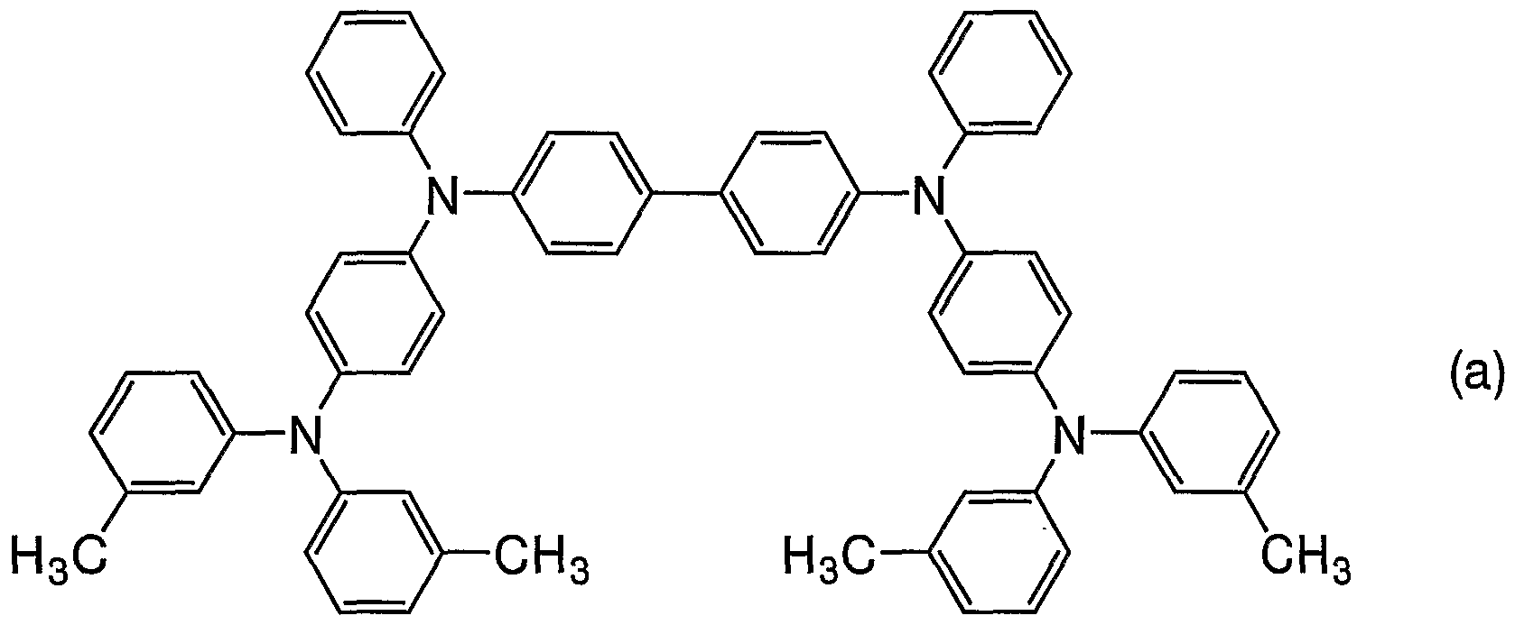


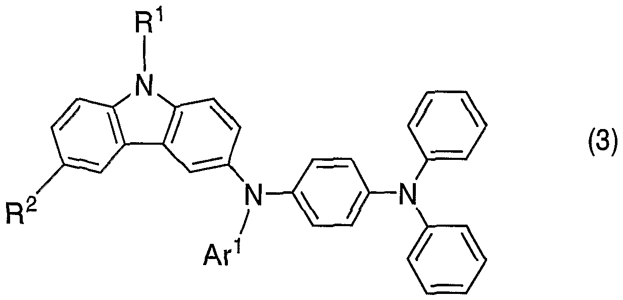


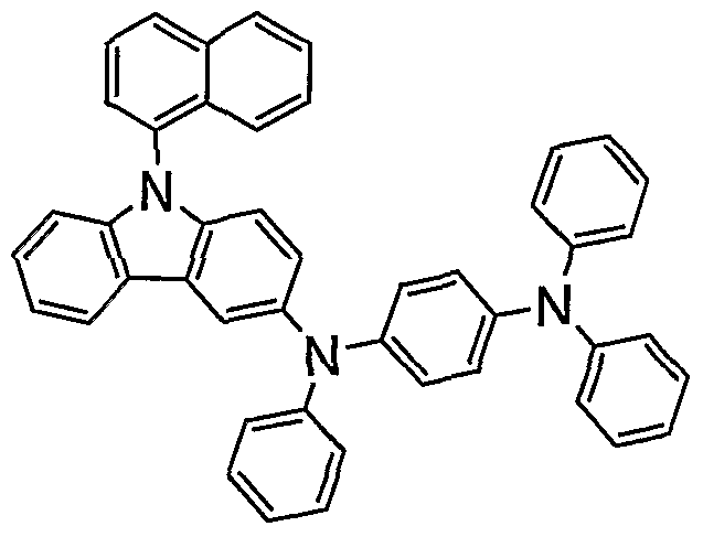


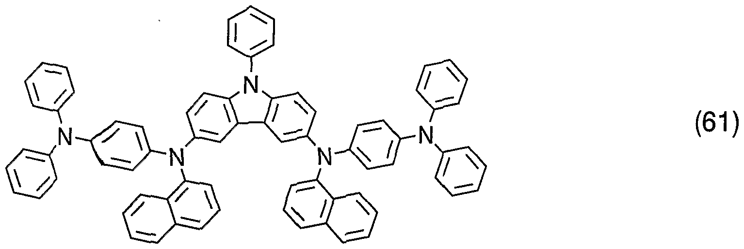


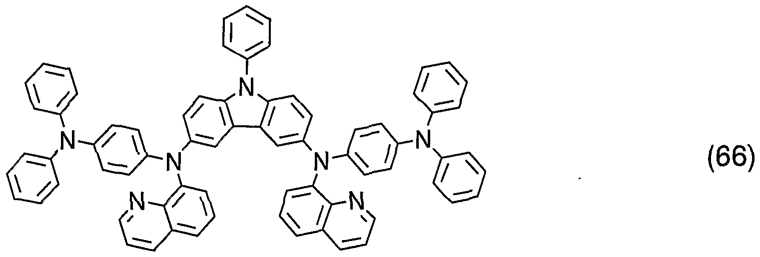


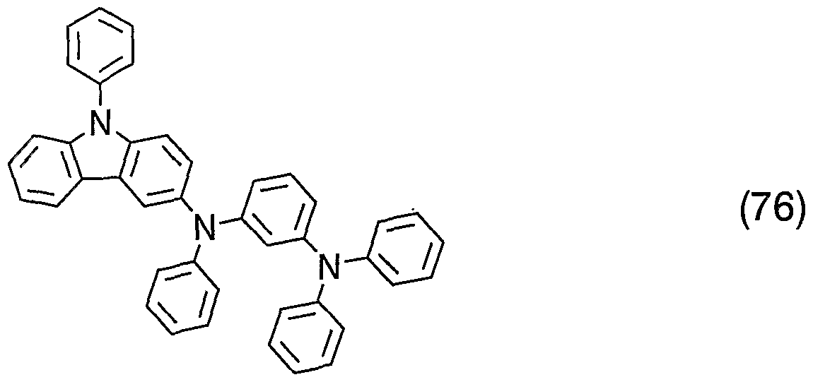


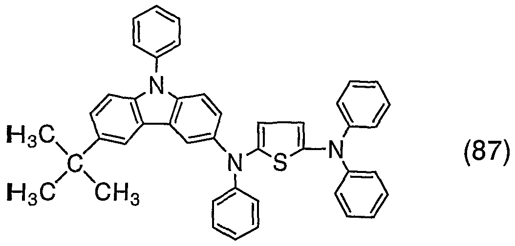


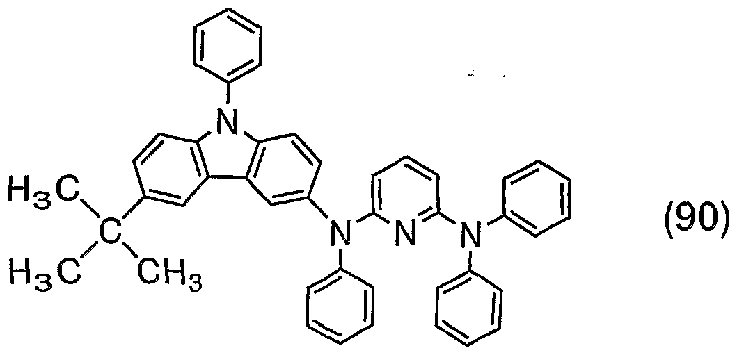


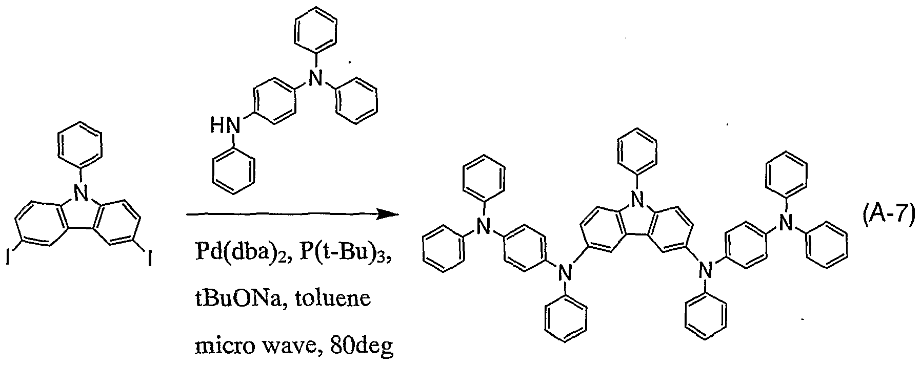


Claims


Priority Applications (5)
| Application Number | Priority Date | Filing Date | Title |
|---|---|---|---|
| EP05795774.8A EP1805140B1 (en) | 2004-10-19 | 2005-10-14 | Carbazole derivative, and light emitting element and light emitting device using the carbazole derivative |
| US10/583,028 US7901791B2 (en) | 2004-10-19 | 2005-10-14 | Carbazole derivative, and light emitting element and light emitting device using the carbazole derivative |
| CN200580035385.4A CN101039909B (en) | 2004-10-19 | 2005-10-14 | Carbazole derivative, and light emitting element and light emitting device using the carbazole derivative |
| US13/037,392 US8431248B2 (en) | 2004-10-19 | 2011-03-01 | Carbazole derivative, and light emitting element and light emitting device using the carbazole derivative |
| US13/865,363 US8900728B2 (en) | 2004-10-19 | 2013-04-18 | Carbazole derivative, and light emitting element and light emitting device using the carbazole derivative |
Applications Claiming Priority (6)
| Application Number | Priority Date | Filing Date | Title |
|---|---|---|---|
| JP2004304225 | 2004-10-19 | ||
| JP2004-304225 | 2004-10-19 | ||
| JP2004333344 | 2004-11-17 | ||
| JP2004-333344 | 2004-11-17 | ||
| JP2005-084533 | 2005-03-23 | ||
| JP2005084533 | 2005-03-23 |
Related Child Applications (2)
| Application Number | Title | Priority Date | Filing Date |
|---|---|---|---|
| US10/583,028 A-371-Of-International US7901791B2 (en) | 2004-10-19 | 2005-10-14 | Carbazole derivative, and light emitting element and light emitting device using the carbazole derivative |
| US13/037,392 Continuation US8431248B2 (en) | 2004-10-19 | 2011-03-01 | Carbazole derivative, and light emitting element and light emitting device using the carbazole derivative |
Publications (1)
| Publication Number | Publication Date |
|---|---|
| WO2006043647A1 true WO2006043647A1 (en) | 2006-04-27 |
Family
ID=36203063
Family Applications (1)
| Application Number | Title | Priority Date | Filing Date |
|---|---|---|---|
| PCT/JP2005/019349 WO2006043647A1 (en) | 2004-10-19 | 2005-10-14 | Carbazole derivative, and light emitting element and light emitting device using the carbazole derivative |
Country Status (5)
| Country | Link |
|---|---|
| US (3) | US7901791B2 (en) |
| EP (1) | EP1805140B1 (en) |
| JP (1) | JP5433715B2 (en) |
| CN (2) | CN101039909B (en) |
| WO (1) | WO2006043647A1 (en) |
Cited By (8)
| Publication number | Priority date | Publication date | Assignee | Title |
|---|---|---|---|---|
| WO2007020804A1 (en) * | 2005-08-12 | 2007-02-22 | Semiconductor Energy Laboratory Co., Ltd. | Arylamine compound and synthetic method thereof |
| WO2007043484A1 (en) * | 2005-10-07 | 2007-04-19 | Toyo Ink Manufacturing Co., Ltd. | Carbazole-containing amine compound and use thereof |
| WO2008010377A1 (en) * | 2006-07-21 | 2008-01-24 | Toyo Ink Manufacturing Co., Ltd. | Carbazole-containing amine compound and use thereof |
| JP2008044923A (en) * | 2005-10-07 | 2008-02-28 | Toyo Ink Mfg Co Ltd | Carbazole-containing amine compound and its use |
| WO2009061156A1 (en) * | 2007-11-08 | 2009-05-14 | Lg Chem, Ltd. | New compound and organic light emitting device using the same |
| WO2009061145A1 (en) * | 2007-11-08 | 2009-05-14 | Lg Chem, Ltd. | New compound and organic light emitting device using the same |
| US8900728B2 (en) | 2004-10-19 | 2014-12-02 | Semiconductor Energy Laboratory Co., Ltd. | Carbazole derivative, and light emitting element and light emitting device using the carbazole derivative |
| US9142783B2 (en) | 2004-11-30 | 2015-09-22 | Semiconductor Energy Laboratory Co., Ltd. | Light emitting element and light emitting device |
Families Citing this family (19)
| Publication number | Priority date | Publication date | Assignee | Title |
|---|---|---|---|---|
| JP5242917B2 (en) * | 2004-03-19 | 2013-07-24 | エルジー・ケム・リミテッド | Novel hole injection or transport material and organic light emitting device using the same |
| WO2007086534A1 (en) | 2006-01-26 | 2007-08-02 | Semiconductor Energy Laboratory Co., Ltd. | Organic field effect transistor and semiconductor device |
| EP2066629B1 (en) * | 2006-09-28 | 2017-05-17 | Semiconductor Energy Laboratory Co, Ltd. | Anthracene derivative, and light emitting element, light emitting device, and electronic device using the anthracene derivative |
| TWI480277B (en) * | 2009-03-20 | 2015-04-11 | Semiconductor Energy Lab | Carbazole derivative with heteroaromatic ring, and light-emitting element, light-emitting device, and electronic device using carbazole derivative with heteroaromatic ring |
| JP2010254671A (en) * | 2009-03-31 | 2010-11-11 | Semiconductor Energy Lab Co Ltd | Carbazole derivative, material for use in light emitting element, light emitting element, light emitting apparatus, electronic equipment, and illumination apparatus |
| KR101935710B1 (en) | 2009-10-20 | 2019-04-05 | 토소가부시키가이샤 | Carbazole compound and use thereof |
| EP2354135B1 (en) * | 2009-12-23 | 2013-09-18 | Semiconductor Energy Laboratory Co., Ltd. | Benzimidazol-2-yl-phenyl compound, light-emitting element, light-emitting device, electronic device, and lighting device |
| JP5623996B2 (en) | 2010-09-21 | 2014-11-12 | 株式会社半導体エネルギー研究所 | Carbazole derivatives |
| JP5872861B2 (en) * | 2010-11-30 | 2016-03-01 | 株式会社半導体エネルギー研究所 | Carbazole compounds |
| US9450192B2 (en) * | 2010-12-06 | 2016-09-20 | E-Ray Optoelectronics Technology | Carbazole derivative and organic electroluminescent devices utilizing the same and fabrication method thereof |
| KR102021273B1 (en) | 2011-05-27 | 2019-09-16 | 가부시키가이샤 한도오따이 에네루기 켄큐쇼 | Carbazole compound, light-emitting element, light-emitting device, electronic device, and lighting device |
| US9051274B2 (en) | 2011-06-24 | 2015-06-09 | Semiconductor Energy Laboratory Co., Ltd. | Triarylamine compound, light-emitting element, light-emitting device, electronic device, and lighting device |
| WO2013062043A1 (en) | 2011-10-26 | 2013-05-02 | 東ソー株式会社 | 4-aminocarbazole compound and use of same |
| CN103204846A (en) * | 2012-01-12 | 2013-07-17 | 昱镭光电科技股份有限公司 | Carbazole derivative, organic electroluminescent device thereof, and manufacturing method of device |
| KR20140071897A (en) | 2012-11-26 | 2014-06-12 | 가부시키가이샤 한도오따이 에네루기 켄큐쇼 | Light-emitting element, light-emitting device, electronic device, and lighting device |
| CN103855311A (en) * | 2012-11-30 | 2014-06-11 | 海洋王照明科技股份有限公司 | Organic electroluminescence device and preparation method thereof |
| US9991471B2 (en) * | 2014-12-26 | 2018-06-05 | Semiconductor Energy Laboratory Co., Ltd. | Light-emitting element, light-emitting device, display device, and electronic device |
| CN106631987A (en) * | 2016-09-30 | 2017-05-10 | 齐鲁工业大学 | Crystal structure of type-A 3,6-diiodo-N-phenylcarbazole and preparation method of crystal structure |
| CN106631986A (en) * | 2016-09-30 | 2017-05-10 | 齐鲁工业大学 | Crystal structure for B-type 3,6-diiodo-N-phenylcarbazole and preparation method thereof |
Citations (9)
| Publication number | Priority date | Publication date | Assignee | Title |
|---|---|---|---|---|
| JPH0689040A (en) * | 1992-09-07 | 1994-03-29 | Ricoh Co Ltd | Electrophotographic sensitive body |
| JPH06346049A (en) * | 1993-06-11 | 1994-12-20 | Toyo Ink Mfg Co Ltd | Organic electro-luminescent element |
| WO2003008515A1 (en) * | 2001-07-17 | 2003-01-30 | Cdt Oxford Limited | Tertiary diamines containing heterocyclic groups and their use in organic electroluminescent devices |
| US20030129448A1 (en) * | 2001-10-19 | 2003-07-10 | Lightronik Technology Inc. | Organic EL device |
| WO2003064373A1 (en) * | 2002-01-28 | 2003-08-07 | Sensient Imaging Technologies Gmbh | Triarylamine derivatives and the use thereof in organic electroluminescent and electrophotographic devices |
| JP2004026732A (en) * | 2002-06-26 | 2004-01-29 | Mitsubishi Chemicals Corp | Asymmetric 1,4-phenylenediamine derivative, and organic electroluminescent device using the same |
| JP2004323509A (en) * | 2003-04-07 | 2004-11-18 | Mitsubishi Chemicals Corp | 2,7-diaminonaphthalene compound, electric charge transporting material, material for organic electroluminescent element and the organic electroluminescent element |
| WO2005090512A1 (en) * | 2004-03-19 | 2005-09-29 | Lg Chem, Ltd. | New materials for injecting or transporting holes and organic electroluminescence devices using the same |
| US20050221124A1 (en) * | 2004-04-02 | 2005-10-06 | Seok-Hwan Hwang | Fluorene-based compound and organic electroluminescent display device using the same |
Family Cites Families (20)
| Publication number | Priority date | Publication date | Assignee | Title |
|---|---|---|---|---|
| JP2501198B2 (en) * | 1986-05-30 | 1996-05-29 | キヤノン株式会社 | Electrophotographic photoreceptor |
| JPH03210481A (en) | 1990-01-12 | 1991-09-13 | Olympus Optical Co Ltd | Movable probe type multipoint contact apparatus for inspecting printed circuit board |
| JPH0532016A (en) | 1991-07-30 | 1993-02-09 | Canon Inc | Mode switching and device therefor |
| JP3210481B2 (en) | 1993-04-30 | 2001-09-17 | バンドー化学株式会社 | 1,3,5-tris [4- (N-carbazolyl) phenyl] benzene derivative |
| JP3650218B2 (en) | 1996-05-10 | 2005-05-18 | ケミプロ化成株式会社 | High molecular weight aromatic amine compound and hole transporting material comprising the same |
| JP4088985B2 (en) | 1997-05-09 | 2008-05-21 | コニカミノルタホールディングス株式会社 | Organic electroluminescence device using new amino compound |
| CN1748017A (en) * | 2003-02-12 | 2006-03-15 | 皇家飞利浦电子股份有限公司 | Carbazole compounds and use of such compounds in organic electroluminescent devices |
| WO2005040117A1 (en) | 2003-10-27 | 2005-05-06 | Semiconductor Energy Laboratory Co., Ltd. | Carbazole derivative, light emitting element, and light emitting device |
| KR100846586B1 (en) | 2006-05-29 | 2008-07-16 | 삼성에스디아이 주식회사 | An organic light emitting device and a flat panel display device comprising the same |
| KR100787425B1 (en) | 2004-11-29 | 2007-12-26 | 삼성에스디아이 주식회사 | Phenylcarbazole-based compound and Organic electroluminescence display employing the same |
| US8188315B2 (en) | 2004-04-02 | 2012-05-29 | Samsung Mobile Display Co., Ltd. | Organic light emitting device and flat panel display device comprising the same |
| KR100669716B1 (en) | 2004-07-14 | 2007-01-16 | 삼성에스디아이 주식회사 | Phenylcarbazole compounds and organic electroluminescence devices using the same |
| US20070249867A1 (en) | 2004-08-11 | 2007-10-25 | Harue Nakashima | Method for Synthesis of Aromatic Amine |
| JP5032016B2 (en) * | 2004-10-19 | 2012-09-26 | 株式会社半導体エネルギー研究所 | CARBAZOLE DERIVATIVE, LIGHT EMITTING ELEMENT USING CARBAZOLE DERIVATIVE, AND LIGHT EMITTING DEVICE |
| CN101039909B (en) * | 2004-10-19 | 2011-04-20 | 株式会社半导体能源研究所 | Carbazole derivative, and light emitting element and light emitting device using the carbazole derivative |
| US8021765B2 (en) | 2004-11-29 | 2011-09-20 | Samsung Mobile Display Co., Ltd. | Phenylcarbazole-based compound and organic electroluminescent device employing the same |
| CN101847690B (en) | 2004-11-30 | 2012-08-08 | 株式会社半导体能源研究所 | Light emitting element and light emitting device |
| US20080254318A1 (en) | 2004-12-28 | 2008-10-16 | Semiconductor Energy Laboratory Co., Ltd. | Carbazole Derivative, and Light-Emitting Element and Light-Emitting Device Using the Carbzole Derivative |
| WO2007020804A1 (en) | 2005-08-12 | 2007-02-22 | Semiconductor Energy Laboratory Co., Ltd. | Arylamine compound and synthetic method thereof |
| JP2007284411A (en) | 2006-04-20 | 2007-11-01 | Bando Chem Ind Ltd | New carbazole derivative and its utilization |
-
2005
- 2005-10-14 CN CN200580035385.4A patent/CN101039909B/en not_active Expired - Fee Related
- 2005-10-14 US US10/583,028 patent/US7901791B2/en not_active Expired - Fee Related
- 2005-10-14 EP EP05795774.8A patent/EP1805140B1/en not_active Expired - Fee Related
- 2005-10-14 WO PCT/JP2005/019349 patent/WO2006043647A1/en active Application Filing
- 2005-10-14 CN CN201110037442.XA patent/CN102153502B/en not_active Expired - Fee Related
-
2011
- 2011-03-01 US US13/037,392 patent/US8431248B2/en active Active
-
2012
- 2012-02-13 JP JP2012028557A patent/JP5433715B2/en not_active Expired - Fee Related
-
2013
- 2013-04-18 US US13/865,363 patent/US8900728B2/en not_active Expired - Fee Related
Patent Citations (9)
| Publication number | Priority date | Publication date | Assignee | Title |
|---|---|---|---|---|
| JPH0689040A (en) * | 1992-09-07 | 1994-03-29 | Ricoh Co Ltd | Electrophotographic sensitive body |
| JPH06346049A (en) * | 1993-06-11 | 1994-12-20 | Toyo Ink Mfg Co Ltd | Organic electro-luminescent element |
| WO2003008515A1 (en) * | 2001-07-17 | 2003-01-30 | Cdt Oxford Limited | Tertiary diamines containing heterocyclic groups and their use in organic electroluminescent devices |
| US20030129448A1 (en) * | 2001-10-19 | 2003-07-10 | Lightronik Technology Inc. | Organic EL device |
| WO2003064373A1 (en) * | 2002-01-28 | 2003-08-07 | Sensient Imaging Technologies Gmbh | Triarylamine derivatives and the use thereof in organic electroluminescent and electrophotographic devices |
| JP2004026732A (en) * | 2002-06-26 | 2004-01-29 | Mitsubishi Chemicals Corp | Asymmetric 1,4-phenylenediamine derivative, and organic electroluminescent device using the same |
| JP2004323509A (en) * | 2003-04-07 | 2004-11-18 | Mitsubishi Chemicals Corp | 2,7-diaminonaphthalene compound, electric charge transporting material, material for organic electroluminescent element and the organic electroluminescent element |
| WO2005090512A1 (en) * | 2004-03-19 | 2005-09-29 | Lg Chem, Ltd. | New materials for injecting or transporting holes and organic electroluminescence devices using the same |
| US20050221124A1 (en) * | 2004-04-02 | 2005-10-06 | Seok-Hwan Hwang | Fluorene-based compound and organic electroluminescent display device using the same |
Non-Patent Citations (1)
| Title |
|---|
| See also references of EP1805140A4 * |
Cited By (10)
| Publication number | Priority date | Publication date | Assignee | Title |
|---|---|---|---|---|
| US8900728B2 (en) | 2004-10-19 | 2014-12-02 | Semiconductor Energy Laboratory Co., Ltd. | Carbazole derivative, and light emitting element and light emitting device using the carbazole derivative |
| US9142783B2 (en) | 2004-11-30 | 2015-09-22 | Semiconductor Energy Laboratory Co., Ltd. | Light emitting element and light emitting device |
| WO2007020804A1 (en) * | 2005-08-12 | 2007-02-22 | Semiconductor Energy Laboratory Co., Ltd. | Arylamine compound and synthetic method thereof |
| WO2007043484A1 (en) * | 2005-10-07 | 2007-04-19 | Toyo Ink Manufacturing Co., Ltd. | Carbazole-containing amine compound and use thereof |
| JP2008044923A (en) * | 2005-10-07 | 2008-02-28 | Toyo Ink Mfg Co Ltd | Carbazole-containing amine compound and its use |
| WO2008010377A1 (en) * | 2006-07-21 | 2008-01-24 | Toyo Ink Manufacturing Co., Ltd. | Carbazole-containing amine compound and use thereof |
| WO2009061156A1 (en) * | 2007-11-08 | 2009-05-14 | Lg Chem, Ltd. | New compound and organic light emitting device using the same |
| WO2009061145A1 (en) * | 2007-11-08 | 2009-05-14 | Lg Chem, Ltd. | New compound and organic light emitting device using the same |
| US8395143B2 (en) | 2007-11-08 | 2013-03-12 | Lg Chem, Ltd. | Compound and organic light emitting device using the same |
| US8968884B2 (en) | 2007-11-08 | 2015-03-03 | Lg Chem, Ltd. | Compound and organic light emitting device using the same |
Also Published As
| Publication number | Publication date |
|---|---|
| JP5433715B2 (en) | 2014-03-05 |
| US20130228765A1 (en) | 2013-09-05 |
| EP1805140A1 (en) | 2007-07-11 |
| CN102153502A (en) | 2011-08-17 |
| US20110147730A1 (en) | 2011-06-23 |
| EP1805140A4 (en) | 2010-07-21 |
| JP2012140436A (en) | 2012-07-26 |
| CN101039909A (en) | 2007-09-19 |
| EP1805140B1 (en) | 2016-08-31 |
| CN102153502B (en) | 2012-12-26 |
| US20080284328A1 (en) | 2008-11-20 |
| US7901791B2 (en) | 2011-03-08 |
| CN101039909B (en) | 2011-04-20 |
| US8900728B2 (en) | 2014-12-02 |
| US8431248B2 (en) | 2013-04-30 |
Similar Documents
| Publication | Publication Date | Title |
|---|---|---|
| EP1805140B1 (en) | Carbazole derivative, and light emitting element and light emitting device using the carbazole derivative | |
| JP5581346B2 (en) | LIGHT EMITTING ELEMENT, LIGHT EMITTING DEVICE AND ELECTRIC DEVICE | |
| JP5032016B2 (en) | CARBAZOLE DERIVATIVE, LIGHT EMITTING ELEMENT USING CARBAZOLE DERIVATIVE, AND LIGHT EMITTING DEVICE | |
| KR101540037B1 (en) | Quinoxaline derivative, and light emitting element, light emitting device, and electronic appliance using the same | |
| US9142783B2 (en) | Light emitting element and light emitting device | |
| JP4975318B2 (en) | CARBAZOLE DERIVATIVE, LIGHT EMITTING ELEMENT USING CARBAZOLE DERIVATIVE, AND LIGHT EMITTING DEVICE | |
| JPWO2005009979A1 (en) | Quinoxaline derivative and light emitting device using the same | |
| KR101288588B1 (en) | Arylamine compound and synthetic method thereof | |
| JP5072293B2 (en) | Quinoxaline derivative, and light-emitting element, light-emitting device, and electronic device using quinoxaline derivative | |
| JP5401007B2 (en) | Aromatic amine compounds, light-emitting elements, light-emitting devices, electronic equipment | |
| JP4869690B2 (en) | LIGHT EMITTING ELEMENT, LIGHT EMITTING DEVICE AND COMPOSITE MATERIAL | |
| JP2007070352A (en) | Arylamine compound and its synthesis method, and light emitting element material, light emitting element and electronic device obtained by using the arylamine compound |
Legal Events
| Date | Code | Title | Description |
|---|---|---|---|
| AK | Designated states |
Kind code of ref document: A1 Designated state(s): AE AG AL AM AT AU AZ BA BB BG BR BW BY BZ CA CH CN CO CR CU CZ DE DK DM DZ EC EE EG ES FI GB GD GE GH GM HR HU ID IL IN IS JP KE KG KM KP KR KZ LC LK LR LS LT LU LV LY MA MD MG MK MN MW MX MZ NA NG NI NO NZ OM PG PH PL PT RO RU SC SD SE SG SK SL SM SY TJ TM TN TR TT TZ UA UG US UZ VC VN YU ZA ZM ZW |
|
| AL | Designated countries for regional patents |
Kind code of ref document: A1 Designated state(s): GM KE LS MW MZ NA SD SL SZ TZ UG ZM ZW AM AZ BY KG KZ MD RU TJ TM AT BE BG CH CY CZ DE DK EE ES FI FR GB GR HU IE IS IT LT LU LV MC NL PL PT RO SE SI SK TR BF BJ CF CG CI CM GA GN GQ GW ML MR NE SN TD TG |
|
| WWE | Wipo information: entry into national phase |
Ref document number: 10583028 Country of ref document: US |
|
| 121 | Ep: the epo has been informed by wipo that ep was designated in this application | ||
| REEP | Request for entry into the european phase |
Ref document number: 2005795774 Country of ref document: EP |
|
| WWE | Wipo information: entry into national phase |
Ref document number: 2005795774 Country of ref document: EP |
|
| WWE | Wipo information: entry into national phase |
Ref document number: 200580035385.4 Country of ref document: CN |
|
| NENP | Non-entry into the national phase |
Ref country code: DE |
|
| WWP | Wipo information: published in national office |
Ref document number: 2005795774 Country of ref document: EP |
|
| NENP | Non-entry into the national phase |
Ref country code: JP |