WO2002086978A1 - Dispositif photoemetteur - Google Patents
Dispositif photoemetteur Download PDFInfo
- Publication number
- WO2002086978A1 WO2002086978A1 PCT/JP2002/003901 JP0203901W WO02086978A1 WO 2002086978 A1 WO2002086978 A1 WO 2002086978A1 JP 0203901 W JP0203901 W JP 0203901W WO 02086978 A1 WO02086978 A1 WO 02086978A1
- Authority
- WO
- WIPO (PCT)
- Prior art keywords
- light emitting
- fluorescent substance
- emitting device
- light
- fluorescent
- Prior art date
Links
- 239000000126 substance Substances 0.000 claims abstract description 403
- 238000000295 emission spectrum Methods 0.000 claims abstract description 55
- 238000004020 luminiscence type Methods 0.000 claims abstract description 4
- 239000004065 semiconductor Substances 0.000 claims description 150
- OAICVXFJPJFONN-UHFFFAOYSA-N Phosphorus Chemical compound [P] OAICVXFJPJFONN-UHFFFAOYSA-N 0.000 claims description 106
- 239000000463 material Substances 0.000 claims description 100
- 150000004767 nitrides Chemical class 0.000 claims description 48
- 229910052725 zinc Inorganic materials 0.000 claims description 37
- 239000000203 mixture Substances 0.000 claims description 36
- 229910052749 magnesium Inorganic materials 0.000 claims description 31
- NJPPVKZQTLUDBO-UHFFFAOYSA-N novaluron Chemical compound C1=C(Cl)C(OC(F)(F)C(OC(F)(F)F)F)=CC=C1NC(=O)NC(=O)C1=C(F)C=CC=C1F NJPPVKZQTLUDBO-UHFFFAOYSA-N 0.000 claims description 31
- 229910052791 calcium Inorganic materials 0.000 claims description 30
- -1 cerium-activated yttrium aluminum oxide Chemical class 0.000 claims description 30
- 229910052712 strontium Inorganic materials 0.000 claims description 30
- 238000001228 spectrum Methods 0.000 claims description 29
- 229910052788 barium Inorganic materials 0.000 claims description 28
- 229910052736 halogen Inorganic materials 0.000 claims description 28
- 230000000295 complement effect Effects 0.000 claims description 27
- 229910052748 manganese Inorganic materials 0.000 claims description 26
- 229910052784 alkaline earth metal Inorganic materials 0.000 claims description 23
- 229910052794 bromium Inorganic materials 0.000 claims description 23
- 150000001342 alkaline earth metals Chemical class 0.000 claims description 22
- 229910052804 chromium Inorganic materials 0.000 claims description 22
- 229910052742 iron Inorganic materials 0.000 claims description 22
- 150000002367 halogens Chemical class 0.000 claims description 20
- 229910052718 tin Inorganic materials 0.000 claims description 20
- 229910052731 fluorine Inorganic materials 0.000 claims description 17
- 239000010931 gold Substances 0.000 claims description 17
- 229910052740 iodine Inorganic materials 0.000 claims description 17
- 229910052801 chlorine Inorganic materials 0.000 claims description 16
- BASFCYQUMIYNBI-UHFFFAOYSA-N platinum Chemical group [Pt] BASFCYQUMIYNBI-UHFFFAOYSA-N 0.000 claims description 14
- 125000005843 halogen group Chemical group 0.000 claims description 13
- 229910052688 Gadolinium Inorganic materials 0.000 claims description 12
- 229910052737 gold Inorganic materials 0.000 claims description 12
- 229910052684 Cerium Inorganic materials 0.000 claims description 11
- 229910052733 gallium Inorganic materials 0.000 claims description 10
- PCHJSUWPFVWCPO-UHFFFAOYSA-N gold Chemical compound [Au] PCHJSUWPFVWCPO-UHFFFAOYSA-N 0.000 claims description 10
- 229910052738 indium Inorganic materials 0.000 claims description 10
- 229910052727 yttrium Inorganic materials 0.000 claims description 9
- 229910052586 apatite Inorganic materials 0.000 claims description 8
- 229910052799 carbon Inorganic materials 0.000 claims description 8
- 229910052802 copper Inorganic materials 0.000 claims description 8
- VSIIXMUUUJUKCM-UHFFFAOYSA-D pentacalcium;fluoride;triphosphate Chemical compound [F-].[Ca+2].[Ca+2].[Ca+2].[Ca+2].[Ca+2].[O-]P([O-])([O-])=O.[O-]P([O-])([O-])=O.[O-]P([O-])([O-])=O VSIIXMUUUJUKCM-UHFFFAOYSA-D 0.000 claims description 8
- 229910052746 lanthanum Inorganic materials 0.000 claims description 7
- JNDMLEXHDPKVFC-UHFFFAOYSA-N aluminum;oxygen(2-);yttrium(3+) Chemical class [O-2].[O-2].[O-2].[Al+3].[Y+3] JNDMLEXHDPKVFC-UHFFFAOYSA-N 0.000 claims description 5
- 229910052751 metal Inorganic materials 0.000 claims description 5
- 239000002184 metal Substances 0.000 claims description 5
- 229910052796 boron Inorganic materials 0.000 claims description 4
- 230000003287 optical effect Effects 0.000 claims description 4
- 229910020314 ClBr Inorganic materials 0.000 claims 1
- 239000000919 ceramic Substances 0.000 claims 1
- 239000002994 raw material Substances 0.000 description 59
- 229910002601 GaN Inorganic materials 0.000 description 46
- 230000005284 excitation Effects 0.000 description 45
- 239000002245 particle Substances 0.000 description 37
- 239000011777 magnesium Substances 0.000 description 32
- 238000009877 rendering Methods 0.000 description 28
- 229910017855 NH 4 F Inorganic materials 0.000 description 21
- 238000006243 chemical reaction Methods 0.000 description 21
- 239000000758 substrate Substances 0.000 description 19
- 239000011230 binding agent Substances 0.000 description 18
- 229910052594 sapphire Inorganic materials 0.000 description 17
- 239000010980 sapphire Substances 0.000 description 17
- 239000010408 film Substances 0.000 description 16
- 238000000034 method Methods 0.000 description 15
- 230000008859 change Effects 0.000 description 13
- 239000003086 colorant Substances 0.000 description 13
- 230000007423 decrease Effects 0.000 description 13
- 125000004435 hydrogen atom Chemical group [H]* 0.000 description 12
- XLYOFNOQVPJJNP-UHFFFAOYSA-N water Substances O XLYOFNOQVPJJNP-UHFFFAOYSA-N 0.000 description 12
- 239000003795 chemical substances by application Substances 0.000 description 11
- 239000002002 slurry Substances 0.000 description 11
- QGZKDVFQNNGYKY-UHFFFAOYSA-N Ammonia Chemical compound N QGZKDVFQNNGYKY-UHFFFAOYSA-N 0.000 description 10
- 239000000460 chlorine Substances 0.000 description 10
- 150000001875 compounds Chemical class 0.000 description 10
- 238000000695 excitation spectrum Methods 0.000 description 10
- 239000000945 filler Substances 0.000 description 10
- VYPSYNLAJGMNEJ-UHFFFAOYSA-N Silicium dioxide Chemical compound O=[Si]=O VYPSYNLAJGMNEJ-UHFFFAOYSA-N 0.000 description 9
- 238000009826 distribution Methods 0.000 description 9
- 239000011347 resin Substances 0.000 description 9
- 229920005989 resin Polymers 0.000 description 9
- 239000012298 atmosphere Substances 0.000 description 8
- 239000000243 solution Substances 0.000 description 8
- PNEYBMLMFCGWSK-UHFFFAOYSA-N aluminium oxide Inorganic materials [O-2].[O-2].[O-2].[Al+3].[Al+3] PNEYBMLMFCGWSK-UHFFFAOYSA-N 0.000 description 7
- 125000003118 aryl group Chemical group 0.000 description 7
- 230000004888 barrier function Effects 0.000 description 7
- 239000002585 base Substances 0.000 description 7
- 239000013078 crystal Substances 0.000 description 7
- 238000005530 etching Methods 0.000 description 7
- 239000007789 gas Substances 0.000 description 7
- 239000011521 glass Substances 0.000 description 7
- 229910000833 kovar Inorganic materials 0.000 description 7
- 238000004519 manufacturing process Methods 0.000 description 7
- 238000002156 mixing Methods 0.000 description 7
- 229910052717 sulfur Inorganic materials 0.000 description 7
- XCZXGTMEAKBVPV-UHFFFAOYSA-N trimethylgallium Chemical compound C[Ga](C)C XCZXGTMEAKBVPV-UHFFFAOYSA-N 0.000 description 7
- 229910052693 Europium Inorganic materials 0.000 description 6
- MUBZPKHOEPUJKR-UHFFFAOYSA-N Oxalic acid Chemical compound OC(=O)C(O)=O MUBZPKHOEPUJKR-UHFFFAOYSA-N 0.000 description 6
- 229910052782 aluminium Inorganic materials 0.000 description 6
- 230000008901 benefit Effects 0.000 description 6
- 238000010586 diagram Methods 0.000 description 6
- 230000000694 effects Effects 0.000 description 6
- 125000000623 heterocyclic group Chemical group 0.000 description 6
- 239000000843 powder Substances 0.000 description 6
- 229910019655 synthetic inorganic crystalline material Inorganic materials 0.000 description 6
- JMASRVWKEDWRBT-UHFFFAOYSA-N Gallium nitride Chemical compound [Ga]#N JMASRVWKEDWRBT-UHFFFAOYSA-N 0.000 description 5
- 239000000020 Nitrocellulose Substances 0.000 description 5
- XAGFODPZIPBFFR-UHFFFAOYSA-N aluminium Chemical compound [Al] XAGFODPZIPBFFR-UHFFFAOYSA-N 0.000 description 5
- 239000002019 doping agent Substances 0.000 description 5
- 238000005286 illumination Methods 0.000 description 5
- 239000012535 impurity Substances 0.000 description 5
- 229910003465 moissanite Inorganic materials 0.000 description 5
- 229920001220 nitrocellulos Polymers 0.000 description 5
- 229910052698 phosphorus Inorganic materials 0.000 description 5
- 239000010453 quartz Substances 0.000 description 5
- 229910010271 silicon carbide Inorganic materials 0.000 description 5
- IJGRMHOSHXDMSA-UHFFFAOYSA-N Atomic nitrogen Chemical compound N#N IJGRMHOSHXDMSA-UHFFFAOYSA-N 0.000 description 4
- 229910052765 Lutetium Inorganic materials 0.000 description 4
- 229910052779 Neodymium Inorganic materials 0.000 description 4
- 229910052771 Terbium Inorganic materials 0.000 description 4
- 238000010521 absorption reaction Methods 0.000 description 4
- 229910021529 ammonia Inorganic materials 0.000 description 4
- 238000005253 cladding Methods 0.000 description 4
- 239000011248 coating agent Substances 0.000 description 4
- 238000000576 coating method Methods 0.000 description 4
- 230000000052 comparative effect Effects 0.000 description 4
- 238000010438 heat treatment Methods 0.000 description 4
- 125000005842 heteroatom Chemical group 0.000 description 4
- 238000002488 metal-organic chemical vapour deposition Methods 0.000 description 4
- 229910052757 nitrogen Inorganic materials 0.000 description 4
- TWNQGVIAIRXVLR-UHFFFAOYSA-N oxo(oxoalumanyloxy)alumane Chemical compound O=[Al]O[Al]=O TWNQGVIAIRXVLR-UHFFFAOYSA-N 0.000 description 4
- 238000010791 quenching Methods 0.000 description 4
- 230000000171 quenching effect Effects 0.000 description 4
- 229910052706 scandium Inorganic materials 0.000 description 4
- 229910052710 silicon Inorganic materials 0.000 description 4
- 238000006467 substitution reaction Methods 0.000 description 4
- 239000010409 thin film Substances 0.000 description 4
- 230000005457 Black-body radiation Effects 0.000 description 3
- 229910052692 Dysprosium Inorganic materials 0.000 description 3
- KRHYYFGTRYWZRS-UHFFFAOYSA-M Fluoride anion Chemical compound [F-] KRHYYFGTRYWZRS-UHFFFAOYSA-M 0.000 description 3
- BLRPTPMANUNPDV-UHFFFAOYSA-N Silane Chemical compound [SiH4] BLRPTPMANUNPDV-UHFFFAOYSA-N 0.000 description 3
- 230000009471 action Effects 0.000 description 3
- 229910045601 alloy Inorganic materials 0.000 description 3
- 239000000956 alloy Substances 0.000 description 3
- 229910052785 arsenic Inorganic materials 0.000 description 3
- 125000004429 atom Chemical group 0.000 description 3
- 229910052793 cadmium Inorganic materials 0.000 description 3
- 230000007613 environmental effect Effects 0.000 description 3
- 230000004907 flux Effects 0.000 description 3
- 239000002223 garnet Substances 0.000 description 3
- 229910052732 germanium Inorganic materials 0.000 description 3
- 230000002093 peripheral effect Effects 0.000 description 3
- NBIIXXVUZAFLBC-UHFFFAOYSA-K phosphate Chemical compound [O-]P([O-])([O-])=O NBIIXXVUZAFLBC-UHFFFAOYSA-K 0.000 description 3
- 238000001020 plasma etching Methods 0.000 description 3
- 229920001296 polysiloxane Polymers 0.000 description 3
- 229910052761 rare earth metal Inorganic materials 0.000 description 3
- 229910000077 silane Inorganic materials 0.000 description 3
- 238000002834 transmittance Methods 0.000 description 3
- 125000002023 trifluoromethyl group Chemical group FC(F)(F)* 0.000 description 3
- 238000003466 welding Methods 0.000 description 3
- NLXLAEXVIDQMFP-UHFFFAOYSA-N Ammonia chloride Chemical compound [NH4+].[Cl-] NLXLAEXVIDQMFP-UHFFFAOYSA-N 0.000 description 2
- YZCKVEUIGOORGS-OUBTZVSYSA-N Deuterium Chemical compound [2H] YZCKVEUIGOORGS-OUBTZVSYSA-N 0.000 description 2
- RTZKZFJDLAIYFH-UHFFFAOYSA-N Diethyl ether Chemical compound CCOCC RTZKZFJDLAIYFH-UHFFFAOYSA-N 0.000 description 2
- 101100513612 Microdochium nivale MnCO gene Proteins 0.000 description 2
- 229910019142 PO4 Inorganic materials 0.000 description 2
- 229910052772 Samarium Inorganic materials 0.000 description 2
- 229910004298 SiO 2 Inorganic materials 0.000 description 2
- 229910052769 Ytterbium Inorganic materials 0.000 description 2
- 239000002253 acid Substances 0.000 description 2
- 239000012190 activator Substances 0.000 description 2
- 125000003342 alkenyl group Chemical group 0.000 description 2
- 125000003545 alkoxy group Chemical group 0.000 description 2
- 125000000217 alkyl group Chemical group 0.000 description 2
- 125000003710 aryl alkyl group Chemical group 0.000 description 2
- QVGXLLKOCUKJST-UHFFFAOYSA-N atomic oxygen Chemical compound [O] QVGXLLKOCUKJST-UHFFFAOYSA-N 0.000 description 2
- 230000015572 biosynthetic process Effects 0.000 description 2
- 229910052797 bismuth Inorganic materials 0.000 description 2
- 125000000484 butyl group Chemical group [H]C([*])([H])C([H])([H])C([H])([H])C([H])([H])[H] 0.000 description 2
- GWXLDORMOJMVQZ-UHFFFAOYSA-N cerium Chemical compound [Ce] GWXLDORMOJMVQZ-UHFFFAOYSA-N 0.000 description 2
- 125000001309 chloro group Chemical group Cl* 0.000 description 2
- 239000000470 constituent Substances 0.000 description 2
- 229910052805 deuterium Inorganic materials 0.000 description 2
- 239000010419 fine particle Substances 0.000 description 2
- 125000004051 hexyl group Chemical group [H]C([H])([H])C([H])([H])C([H])([H])C([H])([H])C([H])([H])C([H])([H])* 0.000 description 2
- 238000002248 hydride vapour-phase epitaxy Methods 0.000 description 2
- 229910010272 inorganic material Inorganic materials 0.000 description 2
- 239000011147 inorganic material Substances 0.000 description 2
- 229910052745 lead Inorganic materials 0.000 description 2
- 238000002844 melting Methods 0.000 description 2
- ZGEGCLOFRBLKSE-UHFFFAOYSA-N methylene hexane Natural products CCCCCC=C ZGEGCLOFRBLKSE-UHFFFAOYSA-N 0.000 description 2
- 230000004048 modification Effects 0.000 description 2
- 238000012986 modification Methods 0.000 description 2
- 229910052759 nickel Inorganic materials 0.000 description 2
- 125000000449 nitro group Chemical group [O-][N+](*)=O 0.000 description 2
- 239000011368 organic material Substances 0.000 description 2
- 239000003960 organic solvent Substances 0.000 description 2
- 235000006408 oxalic acid Nutrition 0.000 description 2
- 229910052760 oxygen Inorganic materials 0.000 description 2
- 239000001301 oxygen Substances 0.000 description 2
- REIUXOLGHVXAEO-UHFFFAOYSA-N pentadecan-1-ol Chemical compound CCCCCCCCCCCCCCCO REIUXOLGHVXAEO-UHFFFAOYSA-N 0.000 description 2
- 239000010452 phosphate Substances 0.000 description 2
- 238000005424 photoluminescence Methods 0.000 description 2
- 238000001556 precipitation Methods 0.000 description 2
- 230000003252 repetitive effect Effects 0.000 description 2
- 229910052702 rhenium Inorganic materials 0.000 description 2
- SCPYDCQAZCOKTP-UHFFFAOYSA-N silanol Chemical compound [SiH3]O SCPYDCQAZCOKTP-UHFFFAOYSA-N 0.000 description 2
- 229910052709 silver Inorganic materials 0.000 description 2
- 238000004544 sputter deposition Methods 0.000 description 2
- 125000001424 substituent group Chemical group 0.000 description 2
- 238000005979 thermal decomposition reaction Methods 0.000 description 2
- 239000010936 titanium Substances 0.000 description 2
- 229910052719 titanium Inorganic materials 0.000 description 2
- FKTXDTWDCPTPHK-UHFFFAOYSA-N 1,1,1,2,3,3,3-heptafluoropropane Chemical group FC(F)(F)[C](F)C(F)(F)F FKTXDTWDCPTPHK-UHFFFAOYSA-N 0.000 description 1
- 125000004105 2-pyridyl group Chemical group N1=C([*])C([H])=C([H])C([H])=C1[H] 0.000 description 1
- MGYGFNQQGAQEON-UHFFFAOYSA-N 4-tolyl isocyanate Chemical compound CC1=CC=C(N=C=O)C=C1 MGYGFNQQGAQEON-UHFFFAOYSA-N 0.000 description 1
- DDFHBQSCUXNBSA-UHFFFAOYSA-N 5-(5-carboxythiophen-2-yl)thiophene-2-carboxylic acid Chemical compound S1C(C(=O)O)=CC=C1C1=CC=C(C(O)=O)S1 DDFHBQSCUXNBSA-UHFFFAOYSA-N 0.000 description 1
- 239000004925 Acrylic resin Substances 0.000 description 1
- 229920000178 Acrylic resin Polymers 0.000 description 1
- 229910017980 Ag—Sn Inorganic materials 0.000 description 1
- QGZKDVFQNNGYKY-UHFFFAOYSA-O Ammonium Chemical compound [NH4+] QGZKDVFQNNGYKY-UHFFFAOYSA-O 0.000 description 1
- BTBUEUYNUDRHOZ-UHFFFAOYSA-N Borate Chemical compound [O-]B([O-])[O-] BTBUEUYNUDRHOZ-UHFFFAOYSA-N 0.000 description 1
- WKBOTKDWSSQWDR-UHFFFAOYSA-N Bromine atom Chemical group [Br] WKBOTKDWSSQWDR-UHFFFAOYSA-N 0.000 description 1
- VEXZGXHMUGYJMC-UHFFFAOYSA-M Chloride anion Chemical compound [Cl-] VEXZGXHMUGYJMC-UHFFFAOYSA-M 0.000 description 1
- 229910052691 Erbium Inorganic materials 0.000 description 1
- MUDNOQOIUOBFMT-UHFFFAOYSA-N FC1(C(C(C(C=C1)(O)F)(F)F)(F)F)F Chemical compound FC1(C(C(C(C=C1)(O)F)(F)F)(F)F)F MUDNOQOIUOBFMT-UHFFFAOYSA-N 0.000 description 1
- GYHNNYVSQQEPJS-UHFFFAOYSA-N Gallium Chemical compound [Ga] GYHNNYVSQQEPJS-UHFFFAOYSA-N 0.000 description 1
- 229910001218 Gallium arsenide Inorganic materials 0.000 description 1
- 229910052689 Holmium Inorganic materials 0.000 description 1
- FYYHWMGAXLPEAU-UHFFFAOYSA-N Magnesium Chemical compound [Mg] FYYHWMGAXLPEAU-UHFFFAOYSA-N 0.000 description 1
- ISWSIDIOOBJBQZ-UHFFFAOYSA-N Phenol Chemical compound OC1=CC=CC=C1 ISWSIDIOOBJBQZ-UHFFFAOYSA-N 0.000 description 1
- 229910052777 Praseodymium Inorganic materials 0.000 description 1
- 229910001128 Sn alloy Inorganic materials 0.000 description 1
- 229910052775 Thulium Inorganic materials 0.000 description 1
- GWEVSGVZZGPLCZ-UHFFFAOYSA-N Titan oxide Chemical compound O=[Ti]=O GWEVSGVZZGPLCZ-UHFFFAOYSA-N 0.000 description 1
- FHKPLLOSJHHKNU-INIZCTEOSA-N [(3S)-3-[8-(1-ethyl-5-methylpyrazol-4-yl)-9-methylpurin-6-yl]oxypyrrolidin-1-yl]-(oxan-4-yl)methanone Chemical compound C(C)N1N=CC(=C1C)C=1N(C2=NC=NC(=C2N=1)O[C@@H]1CN(CC1)C(=O)C1CCOCC1)C FHKPLLOSJHHKNU-INIZCTEOSA-N 0.000 description 1
- JAWMENYCRQKKJY-UHFFFAOYSA-N [3-(2,4,6,7-tetrahydrotriazolo[4,5-c]pyridin-5-ylmethyl)-1-oxa-2,8-diazaspiro[4.5]dec-2-en-8-yl]-[2-[[3-(trifluoromethoxy)phenyl]methylamino]pyrimidin-5-yl]methanone Chemical compound N1N=NC=2CN(CCC=21)CC1=NOC2(C1)CCN(CC2)C(=O)C=1C=NC(=NC=1)NCC1=CC(=CC=C1)OC(F)(F)F JAWMENYCRQKKJY-UHFFFAOYSA-N 0.000 description 1
- 125000001931 aliphatic group Chemical group 0.000 description 1
- 125000004453 alkoxycarbonyl group Chemical group 0.000 description 1
- 125000005530 alkylenedioxy group Chemical group 0.000 description 1
- PSNPEOOEWZZFPJ-UHFFFAOYSA-N alumane;yttrium Chemical class [AlH3].[Y] PSNPEOOEWZZFPJ-UHFFFAOYSA-N 0.000 description 1
- 235000019270 ammonium chloride Nutrition 0.000 description 1
- RWZYAGGXGHYGMB-UHFFFAOYSA-N anthranilic acid Chemical group NC1=CC=CC=C1C(O)=O RWZYAGGXGHYGMB-UHFFFAOYSA-N 0.000 description 1
- 229910052787 antimony Inorganic materials 0.000 description 1
- 239000007864 aqueous solution Substances 0.000 description 1
- 238000000149 argon plasma sintering Methods 0.000 description 1
- OYLGJCQECKOTOL-UHFFFAOYSA-L barium fluoride Chemical compound [F-].[F-].[Ba+2] OYLGJCQECKOTOL-UHFFFAOYSA-L 0.000 description 1
- 229910001632 barium fluoride Inorganic materials 0.000 description 1
- 229910002113 barium titanate Inorganic materials 0.000 description 1
- JRPBQTZRNDNNOP-UHFFFAOYSA-N barium titanate Chemical compound [Ba+2].[Ba+2].[O-][Ti]([O-])([O-])[O-] JRPBQTZRNDNNOP-UHFFFAOYSA-N 0.000 description 1
- 125000003785 benzimidazolyl group Chemical group N1=C(NC2=C1C=CC=C2)* 0.000 description 1
- 125000001797 benzyl group Chemical group [H]C1=C([H])C([H])=C(C([H])=C1[H])C([H])([H])* 0.000 description 1
- 229910052790 beryllium Inorganic materials 0.000 description 1
- 238000001354 calcination Methods 0.000 description 1
- LEYJJTBJCFGAQN-UHFFFAOYSA-N chembl1985378 Chemical group OC1=CC=C2C=CC=CC2=C1N=NC(C=C1)=CC=C1N=NC1=CC=C(S(O)(=O)=O)C=C1 LEYJJTBJCFGAQN-UHFFFAOYSA-N 0.000 description 1
- 229910052589 chlorapatite Inorganic materials 0.000 description 1
- 239000004020 conductor Substances 0.000 description 1
- 125000004093 cyano group Chemical group *C#N 0.000 description 1
- 125000002704 decyl group Chemical group [H]C([H])([H])C([H])([H])C([H])([H])C([H])([H])C([H])([H])C([H])([H])C([H])([H])C([H])([H])C([H])([H])C([H])([H])* 0.000 description 1
- 230000007547 defect Effects 0.000 description 1
- 239000008367 deionised water Substances 0.000 description 1
- 229910021641 deionized water Inorganic materials 0.000 description 1
- XPPKVPWEQAFLFU-UHFFFAOYSA-J diphosphate(4-) Chemical compound [O-]P([O-])(=O)OP([O-])([O-])=O XPPKVPWEQAFLFU-UHFFFAOYSA-J 0.000 description 1
- 235000011180 diphosphates Nutrition 0.000 description 1
- 238000007599 discharging Methods 0.000 description 1
- 239000006185 dispersion Substances 0.000 description 1
- 238000001035 drying Methods 0.000 description 1
- 239000003822 epoxy resin Substances 0.000 description 1
- 150000002148 esters Chemical class 0.000 description 1
- PROQIPRRNZUXQM-ZXXIGWHRSA-N estriol Chemical compound OC1=CC=C2[C@H]3CC[C@](C)([C@H]([C@H](O)C4)O)[C@@H]4[C@@H]3CCC2=C1 PROQIPRRNZUXQM-ZXXIGWHRSA-N 0.000 description 1
- 238000000605 extraction Methods 0.000 description 1
- 238000010304 firing Methods 0.000 description 1
- 125000001153 fluoro group Chemical group F* 0.000 description 1
- UIWYJDYFSGRHKR-UHFFFAOYSA-N gadolinium atom Chemical compound [Gd] UIWYJDYFSGRHKR-UHFFFAOYSA-N 0.000 description 1
- 125000003187 heptyl group Chemical group [H]C([*])([H])C([H])([H])C([H])([H])C([H])([H])C([H])([H])C([H])([H])C([H])([H])[H] 0.000 description 1
- APFVFJFRJDLVQX-UHFFFAOYSA-N indium atom Chemical compound [In] APFVFJFRJDLVQX-UHFFFAOYSA-N 0.000 description 1
- 238000011835 investigation Methods 0.000 description 1
- 230000001678 irradiating effect Effects 0.000 description 1
- 125000005956 isoquinolyl group Chemical group 0.000 description 1
- 125000000468 ketone group Chemical group 0.000 description 1
- 238000003475 lamination Methods 0.000 description 1
- 150000002603 lanthanum Chemical class 0.000 description 1
- 238000007561 laser diffraction method Methods 0.000 description 1
- 230000031700 light absorption Effects 0.000 description 1
- 239000002932 luster Substances 0.000 description 1
- 230000008018 melting Effects 0.000 description 1
- 238000003801 milling Methods 0.000 description 1
- 239000012299 nitrogen atmosphere Substances 0.000 description 1
- 125000000018 nitroso group Chemical group N(=O)* 0.000 description 1
- KSOCVFUBQIXVDC-FMQUCBEESA-N p-azophenyltrimethylammonium Chemical compound C1=CC([N+](C)(C)C)=CC=C1\N=N\C1=CC=C([N+](C)(C)C)C=C1 KSOCVFUBQIXVDC-FMQUCBEESA-N 0.000 description 1
- 238000000059 patterning Methods 0.000 description 1
- 125000006340 pentafluoro ethyl group Chemical group FC(F)(F)C(F)(F)* 0.000 description 1
- 125000005010 perfluoroalkyl group Chemical group 0.000 description 1
- 125000005460 perfluorocycloalkyl group Chemical group 0.000 description 1
- 125000005561 phenanthryl group Chemical group 0.000 description 1
- 125000000951 phenoxy group Chemical group [H]C1=C([H])C([H])=C(O*)C([H])=C1[H] 0.000 description 1
- 125000001997 phenyl group Chemical group [H]C1=C([H])C([H])=C(*)C([H])=C1[H] 0.000 description 1
- 125000000843 phenylene group Chemical group C1(=C(C=CC=C1)*)* 0.000 description 1
- 229910052699 polonium Inorganic materials 0.000 description 1
- 229920000647 polyepoxide Polymers 0.000 description 1
- 238000004382 potting Methods 0.000 description 1
- 230000008569 process Effects 0.000 description 1
- 125000001725 pyrenyl group Chemical group 0.000 description 1
- 125000004076 pyridyl group Chemical group 0.000 description 1
- 125000000168 pyrrolyl group Chemical group 0.000 description 1
- 125000005493 quinolyl group Chemical group 0.000 description 1
- 230000005855 radiation Effects 0.000 description 1
- 238000000790 scattering method Methods 0.000 description 1
- 238000007789 sealing Methods 0.000 description 1
- 239000003566 sealing material Substances 0.000 description 1
- 238000004062 sedimentation Methods 0.000 description 1
- 229910052711 selenium Inorganic materials 0.000 description 1
- 238000000926 separation method Methods 0.000 description 1
- 230000035939 shock Effects 0.000 description 1
- 229910002027 silica gel Inorganic materials 0.000 description 1
- 239000000741 silica gel Substances 0.000 description 1
- 239000000377 silicon dioxide Substances 0.000 description 1
- 229910052814 silicon oxide Inorganic materials 0.000 description 1
- XGVXKJKTISMIOW-ZDUSSCGKSA-N simurosertib Chemical compound N1N=CC(C=2SC=3C(=O)NC(=NC=3C=2)[C@H]2N3CCC(CC3)C2)=C1C XGVXKJKTISMIOW-ZDUSSCGKSA-N 0.000 description 1
- GCLGEJMYGQKIIW-UHFFFAOYSA-H sodium hexametaphosphate Chemical compound [Na]OP1(=O)OP(=O)(O[Na])OP(=O)(O[Na])OP(=O)(O[Na])OP(=O)(O[Na])OP(=O)(O[Na])O1 GCLGEJMYGQKIIW-UHFFFAOYSA-H 0.000 description 1
- 235000019982 sodium hexametaphosphate Nutrition 0.000 description 1
- 238000003980 solgel method Methods 0.000 description 1
- 239000011029 spinel Substances 0.000 description 1
- 229910052596 spinel Inorganic materials 0.000 description 1
- 239000007858 starting material Substances 0.000 description 1
- 230000001502 supplementing effect Effects 0.000 description 1
- 229910052714 tellurium Inorganic materials 0.000 description 1
- 239000001577 tetrasodium phosphonato phosphate Substances 0.000 description 1
- OGIDPMRJRNCKJF-UHFFFAOYSA-N titanium oxide Inorganic materials [Ti]=O OGIDPMRJRNCKJF-UHFFFAOYSA-N 0.000 description 1
- 125000003866 trichloromethyl group Chemical group ClC(Cl)(Cl)* 0.000 description 1
- 125000000876 trifluoromethoxy group Chemical group FC(F)(F)O* 0.000 description 1
- 239000010981 turquoise Substances 0.000 description 1
- 238000005406 washing Methods 0.000 description 1
- 229910019901 yttrium aluminum garnet Inorganic materials 0.000 description 1
- VWQVUPCCIRVNHF-UHFFFAOYSA-N yttrium atom Chemical compound [Y] VWQVUPCCIRVNHF-UHFFFAOYSA-N 0.000 description 1
- XLOMVQKBTHCTTD-UHFFFAOYSA-N zinc oxide Inorganic materials [Zn]=O XLOMVQKBTHCTTD-UHFFFAOYSA-N 0.000 description 1
Classifications
-
- H—ELECTRICITY
- H01—ELECTRIC ELEMENTS
- H01L—SEMICONDUCTOR DEVICES NOT COVERED BY CLASS H10
- H01L33/00—Semiconductor devices having potential barriers specially adapted for light emission; Processes or apparatus specially adapted for the manufacture or treatment thereof or of parts thereof; Details thereof
- H01L33/48—Semiconductor devices having potential barriers specially adapted for light emission; Processes or apparatus specially adapted for the manufacture or treatment thereof or of parts thereof; Details thereof characterised by the semiconductor body packages
- H01L33/50—Wavelength conversion elements
- H01L33/501—Wavelength conversion elements characterised by the materials, e.g. binder
- H01L33/502—Wavelength conversion materials
- H01L33/504—Elements with two or more wavelength conversion materials
-
- C—CHEMISTRY; METALLURGY
- C09—DYES; PAINTS; POLISHES; NATURAL RESINS; ADHESIVES; COMPOSITIONS NOT OTHERWISE PROVIDED FOR; APPLICATIONS OF MATERIALS NOT OTHERWISE PROVIDED FOR
- C09K—MATERIALS FOR MISCELLANEOUS APPLICATIONS, NOT PROVIDED FOR ELSEWHERE
- C09K11/00—Luminescent, e.g. electroluminescent, chemiluminescent materials
- C09K11/08—Luminescent, e.g. electroluminescent, chemiluminescent materials containing inorganic luminescent materials
- C09K11/58—Luminescent, e.g. electroluminescent, chemiluminescent materials containing inorganic luminescent materials containing copper, silver or gold
- C09K11/582—Chalcogenides
- C09K11/584—Chalcogenides with zinc or cadmium
-
- C—CHEMISTRY; METALLURGY
- C09—DYES; PAINTS; POLISHES; NATURAL RESINS; ADHESIVES; COMPOSITIONS NOT OTHERWISE PROVIDED FOR; APPLICATIONS OF MATERIALS NOT OTHERWISE PROVIDED FOR
- C09K—MATERIALS FOR MISCELLANEOUS APPLICATIONS, NOT PROVIDED FOR ELSEWHERE
- C09K11/00—Luminescent, e.g. electroluminescent, chemiluminescent materials
- C09K11/08—Luminescent, e.g. electroluminescent, chemiluminescent materials containing inorganic luminescent materials
- C09K11/66—Luminescent, e.g. electroluminescent, chemiluminescent materials containing inorganic luminescent materials containing germanium, tin or lead
- C09K11/661—Chalcogenides
- C09K11/662—Chalcogenides with zinc or cadmium
-
- C—CHEMISTRY; METALLURGY
- C09—DYES; PAINTS; POLISHES; NATURAL RESINS; ADHESIVES; COMPOSITIONS NOT OTHERWISE PROVIDED FOR; APPLICATIONS OF MATERIALS NOT OTHERWISE PROVIDED FOR
- C09K—MATERIALS FOR MISCELLANEOUS APPLICATIONS, NOT PROVIDED FOR ELSEWHERE
- C09K11/00—Luminescent, e.g. electroluminescent, chemiluminescent materials
- C09K11/08—Luminescent, e.g. electroluminescent, chemiluminescent materials containing inorganic luminescent materials
- C09K11/77—Luminescent, e.g. electroluminescent, chemiluminescent materials containing inorganic luminescent materials containing rare earth metals
- C09K11/7728—Luminescent, e.g. electroluminescent, chemiluminescent materials containing inorganic luminescent materials containing rare earth metals containing europium
- C09K11/7734—Aluminates
-
- C—CHEMISTRY; METALLURGY
- C09—DYES; PAINTS; POLISHES; NATURAL RESINS; ADHESIVES; COMPOSITIONS NOT OTHERWISE PROVIDED FOR; APPLICATIONS OF MATERIALS NOT OTHERWISE PROVIDED FOR
- C09K—MATERIALS FOR MISCELLANEOUS APPLICATIONS, NOT PROVIDED FOR ELSEWHERE
- C09K11/00—Luminescent, e.g. electroluminescent, chemiluminescent materials
- C09K11/08—Luminescent, e.g. electroluminescent, chemiluminescent materials containing inorganic luminescent materials
- C09K11/77—Luminescent, e.g. electroluminescent, chemiluminescent materials containing inorganic luminescent materials containing rare earth metals
- C09K11/7728—Luminescent, e.g. electroluminescent, chemiluminescent materials containing inorganic luminescent materials containing rare earth metals containing europium
- C09K11/7737—Phosphates
- C09K11/7738—Phosphates with alkaline earth metals
- C09K11/7739—Phosphates with alkaline earth metals with halogens
-
- C—CHEMISTRY; METALLURGY
- C09—DYES; PAINTS; POLISHES; NATURAL RESINS; ADHESIVES; COMPOSITIONS NOT OTHERWISE PROVIDED FOR; APPLICATIONS OF MATERIALS NOT OTHERWISE PROVIDED FOR
- C09K—MATERIALS FOR MISCELLANEOUS APPLICATIONS, NOT PROVIDED FOR ELSEWHERE
- C09K11/00—Luminescent, e.g. electroluminescent, chemiluminescent materials
- C09K11/08—Luminescent, e.g. electroluminescent, chemiluminescent materials containing inorganic luminescent materials
- C09K11/77—Luminescent, e.g. electroluminescent, chemiluminescent materials containing inorganic luminescent materials containing rare earth metals
- C09K11/7766—Luminescent, e.g. electroluminescent, chemiluminescent materials containing inorganic luminescent materials containing rare earth metals containing two or more rare earth metals
- C09K11/7774—Aluminates
-
- C—CHEMISTRY; METALLURGY
- C09—DYES; PAINTS; POLISHES; NATURAL RESINS; ADHESIVES; COMPOSITIONS NOT OTHERWISE PROVIDED FOR; APPLICATIONS OF MATERIALS NOT OTHERWISE PROVIDED FOR
- C09K—MATERIALS FOR MISCELLANEOUS APPLICATIONS, NOT PROVIDED FOR ELSEWHERE
- C09K11/00—Luminescent, e.g. electroluminescent, chemiluminescent materials
- C09K11/08—Luminescent, e.g. electroluminescent, chemiluminescent materials containing inorganic luminescent materials
- C09K11/77—Luminescent, e.g. electroluminescent, chemiluminescent materials containing inorganic luminescent materials containing rare earth metals
- C09K11/7783—Luminescent, e.g. electroluminescent, chemiluminescent materials containing inorganic luminescent materials containing rare earth metals containing two or more rare earth metals one of which being europium
- C09K11/7784—Chalcogenides
- C09K11/7787—Oxides
- C09K11/7789—Oxysulfides
-
- H—ELECTRICITY
- H01—ELECTRIC ELEMENTS
- H01L—SEMICONDUCTOR DEVICES NOT COVERED BY CLASS H10
- H01L33/00—Semiconductor devices having potential barriers specially adapted for light emission; Processes or apparatus specially adapted for the manufacture or treatment thereof or of parts thereof; Details thereof
- H01L33/36—Semiconductor devices having potential barriers specially adapted for light emission; Processes or apparatus specially adapted for the manufacture or treatment thereof or of parts thereof; Details thereof characterised by the electrodes
- H01L33/38—Semiconductor devices having potential barriers specially adapted for light emission; Processes or apparatus specially adapted for the manufacture or treatment thereof or of parts thereof; Details thereof characterised by the electrodes with a particular shape
-
- H—ELECTRICITY
- H05—ELECTRIC TECHNIQUES NOT OTHERWISE PROVIDED FOR
- H05B—ELECTRIC HEATING; ELECTRIC LIGHT SOURCES NOT OTHERWISE PROVIDED FOR; CIRCUIT ARRANGEMENTS FOR ELECTRIC LIGHT SOURCES, IN GENERAL
- H05B33/00—Electroluminescent light sources
- H05B33/12—Light sources with substantially two-dimensional radiating surfaces
- H05B33/14—Light sources with substantially two-dimensional radiating surfaces characterised by the chemical or physical composition or the arrangement of the electroluminescent material, or by the simultaneous addition of the electroluminescent material in or onto the light source
-
- H—ELECTRICITY
- H01—ELECTRIC ELEMENTS
- H01L—SEMICONDUCTOR DEVICES NOT COVERED BY CLASS H10
- H01L2224/00—Indexing scheme for arrangements for connecting or disconnecting semiconductor or solid-state bodies and methods related thereto as covered by H01L24/00
- H01L2224/01—Means for bonding being attached to, or being formed on, the surface to be connected, e.g. chip-to-package, die-attach, "first-level" interconnects; Manufacturing methods related thereto
- H01L2224/42—Wire connectors; Manufacturing methods related thereto
- H01L2224/44—Structure, shape, material or disposition of the wire connectors prior to the connecting process
- H01L2224/45—Structure, shape, material or disposition of the wire connectors prior to the connecting process of an individual wire connector
- H01L2224/45001—Core members of the connector
- H01L2224/45099—Material
- H01L2224/451—Material with a principal constituent of the material being a metal or a metalloid, e.g. boron (B), silicon (Si), germanium (Ge), arsenic (As), antimony (Sb), tellurium (Te) and polonium (Po), and alloys thereof
- H01L2224/45138—Material with a principal constituent of the material being a metal or a metalloid, e.g. boron (B), silicon (Si), germanium (Ge), arsenic (As), antimony (Sb), tellurium (Te) and polonium (Po), and alloys thereof the principal constituent melting at a temperature of greater than or equal to 950°C and less than 1550°C
- H01L2224/45139—Silver (Ag) as principal constituent
-
- H—ELECTRICITY
- H01—ELECTRIC ELEMENTS
- H01L—SEMICONDUCTOR DEVICES NOT COVERED BY CLASS H10
- H01L2224/00—Indexing scheme for arrangements for connecting or disconnecting semiconductor or solid-state bodies and methods related thereto as covered by H01L24/00
- H01L2224/01—Means for bonding being attached to, or being formed on, the surface to be connected, e.g. chip-to-package, die-attach, "first-level" interconnects; Manufacturing methods related thereto
- H01L2224/42—Wire connectors; Manufacturing methods related thereto
- H01L2224/47—Structure, shape, material or disposition of the wire connectors after the connecting process
- H01L2224/48—Structure, shape, material or disposition of the wire connectors after the connecting process of an individual wire connector
- H01L2224/484—Connecting portions
- H01L2224/48463—Connecting portions the connecting portion on the bonding area of the semiconductor or solid-state body being a ball bond
- H01L2224/48465—Connecting portions the connecting portion on the bonding area of the semiconductor or solid-state body being a ball bond the other connecting portion not on the bonding area being a wedge bond, i.e. ball-to-wedge, regular stitch
-
- H—ELECTRICITY
- H01—ELECTRIC ELEMENTS
- H01L—SEMICONDUCTOR DEVICES NOT COVERED BY CLASS H10
- H01L2224/00—Indexing scheme for arrangements for connecting or disconnecting semiconductor or solid-state bodies and methods related thereto as covered by H01L24/00
- H01L2224/01—Means for bonding being attached to, or being formed on, the surface to be connected, e.g. chip-to-package, die-attach, "first-level" interconnects; Manufacturing methods related thereto
- H01L2224/42—Wire connectors; Manufacturing methods related thereto
- H01L2224/47—Structure, shape, material or disposition of the wire connectors after the connecting process
- H01L2224/49—Structure, shape, material or disposition of the wire connectors after the connecting process of a plurality of wire connectors
- H01L2224/4901—Structure
- H01L2224/4903—Connectors having different sizes, e.g. different diameters
-
- H—ELECTRICITY
- H01—ELECTRIC ELEMENTS
- H01L—SEMICONDUCTOR DEVICES NOT COVERED BY CLASS H10
- H01L2224/00—Indexing scheme for arrangements for connecting or disconnecting semiconductor or solid-state bodies and methods related thereto as covered by H01L24/00
- H01L2224/73—Means for bonding being of different types provided for in two or more of groups H01L2224/10, H01L2224/18, H01L2224/26, H01L2224/34, H01L2224/42, H01L2224/50, H01L2224/63, H01L2224/71
- H01L2224/732—Location after the connecting process
- H01L2224/73251—Location after the connecting process on different surfaces
- H01L2224/73265—Layer and wire connectors
-
- H—ELECTRICITY
- H01—ELECTRIC ELEMENTS
- H01L—SEMICONDUCTOR DEVICES NOT COVERED BY CLASS H10
- H01L2924/00—Indexing scheme for arrangements or methods for connecting or disconnecting semiconductor or solid-state bodies as covered by H01L24/00
- H01L2924/0001—Technical content checked by a classifier
- H01L2924/00011—Not relevant to the scope of the group, the symbol of which is combined with the symbol of this group
-
- H—ELECTRICITY
- H01—ELECTRIC ELEMENTS
- H01L—SEMICONDUCTOR DEVICES NOT COVERED BY CLASS H10
- H01L2924/00—Indexing scheme for arrangements or methods for connecting or disconnecting semiconductor or solid-state bodies as covered by H01L24/00
- H01L2924/0001—Technical content checked by a classifier
- H01L2924/00014—Technical content checked by a classifier the subject-matter covered by the group, the symbol of which is combined with the symbol of this group, being disclosed without further technical details
-
- H—ELECTRICITY
- H01—ELECTRIC ELEMENTS
- H01L—SEMICONDUCTOR DEVICES NOT COVERED BY CLASS H10
- H01L33/00—Semiconductor devices having potential barriers specially adapted for light emission; Processes or apparatus specially adapted for the manufacture or treatment thereof or of parts thereof; Details thereof
- H01L33/02—Semiconductor devices having potential barriers specially adapted for light emission; Processes or apparatus specially adapted for the manufacture or treatment thereof or of parts thereof; Details thereof characterised by the semiconductor bodies
- H01L33/20—Semiconductor devices having potential barriers specially adapted for light emission; Processes or apparatus specially adapted for the manufacture or treatment thereof or of parts thereof; Details thereof characterised by the semiconductor bodies with a particular shape, e.g. curved or truncated substrate
-
- H—ELECTRICITY
- H01—ELECTRIC ELEMENTS
- H01L—SEMICONDUCTOR DEVICES NOT COVERED BY CLASS H10
- H01L33/00—Semiconductor devices having potential barriers specially adapted for light emission; Processes or apparatus specially adapted for the manufacture or treatment thereof or of parts thereof; Details thereof
- H01L33/48—Semiconductor devices having potential barriers specially adapted for light emission; Processes or apparatus specially adapted for the manufacture or treatment thereof or of parts thereof; Details thereof characterised by the semiconductor body packages
- H01L33/50—Wavelength conversion elements
- H01L33/501—Wavelength conversion elements characterised by the materials, e.g. binder
- H01L33/502—Wavelength conversion materials
Definitions
- the present invention relates to a light emitting device using a light emitting element and a fluorescent substance, which can be used for a signal light, a lighting, a display, various light sources, and the like, and in particular, is excited by light emission of a semiconductor light emitting element and emits light in a visible region.
- the present invention relates to a white light emitting device using a phosphor having a vector.
- This semiconductor light-emitting device can be driven at low voltage, and has the advantages of small size, light weight, thin shape, long life, high reliability, and low power consumption. Part of the tube is being replaced.
- a light emitting device using a nitride semiconductor has been developed as a light emitting device capable of efficiently emitting light from the ultraviolet region to the short wavelength side of visible light.
- blue and green LEDs with a quantum well structure of 10 or more power have been developed and commercialized using a quantum well structure using a nitride semiconductor (for example, InGaN mixed crystal) as an active (light-emitting) layer. .
- a nitride semiconductor for example, InGaN mixed crystal
- LED chip light emitting element
- fluorescent substance excited by the light to emit fluorescence has enabled mixed color display including white.
- Such a light emitting diode is disclosed, for example, in JP-A-5-152609, JP-A-9-153636, JP-A-10-242413, and the like. .
- the light-emitting element emits blue light having a relatively short wavelength of ultraviolet light or visible light
- the light from the light-emitting element excites a fluorescent substance to emit a visible light having a wavelength longer than that of the light-emitting element. It emits light.
- the structure itself can be simplified and the output can be improved. It has the advantage of being easy to use, but tends to cause color shift.
- a light emitting element that emits ultraviolet light a combination of fluorescent substances capable of emitting RGB (red, green, and blue) is configured to emit white light, and only light emitted from the fluorescent substance is emitted.
- color adjustment can be performed relatively easily.
- a light-emitting element that emits light in the ultraviolet region compared to the case of using a semiconductor light-emitting element that emits visible light, it absorbs some variation in the wavelength of the semiconductor light-emitting element and emits a fluorescent substance. Since chromaticity can be determined only by color, mass productivity can be improved.
- a conventional light emitting device that uses two or more types of fluorescent materials and achieves a predetermined light emission color by mixing colors of light emitted by the fluorescent materials, for example, when the light emission wavelength of a light emitting element, which is excitation light, changes.
- the difference in the excitation spectrum between the two fluorescent substances changes the emission intensity ratio between the two fluorescent substances.
- conventional light-emitting devices are not sufficient to be used as a light source including illumination, taking advantage of the advantages of semiconductor light-emitting elements, and further improvements in luminance and mass productivity are required.
- the mixing ratio of the red fluorescent substance must be increased, and the relative luminance may decrease. Also, when the light is excited on the long wavelength side in the ultraviolet region, the wavelength of the light for exciting the fluorescent substance fluctuates due to the wavelength variation of the light emitting element, causing a decrease in the luminance of the red fluorescent substance, and the change in chromaticity of the light emitting device. It may occur.
- the desired color is adjusted according to the composition of the fluorescent substance. It is hoped that it can be done. Disclosure of the invention
- a first light-emitting device is a light-emitting device including a light-emitting element and a fluorescent substance excited by the light-emitting element.
- the light emitting device has an emission spectrum in a short wavelength region from an ultraviolet region to a visible light, and the fluorescent substance has an emission spectrum having two or more emission peaks, and among the two or more peaks, At least two peaks; characterized by a color relationship.
- the two peaks have a complementary color relationship means that when light having one peak wavelength and light having the other peak wavelength are mixed, light in a white region is obtained. For example, blue and yellow, and blue-green and red.
- the white area includes greenish white, bluish white, purple white, red white and yellowish white.
- one of the two peaks having a complementary color relationship is in the range of 380 nm to 485 nm, and the other peak is 575 nm! It is preferably in the range of 6630 nm.
- “having an emission spectrum in a short wavelength region from the ultraviolet region to the visible light” means that emission is observed between 340 nm and around 450 nm. .
- the first light emitting device according to the present invention configured as described above has a light emitting color of the fluorescent substance that hardly changes even if the light emitting spectrum of the semiconductor light emitting element changes due to manufacturing variations. Variations can be reduced, and uneven color tone can be improved.
- the main light-emitting wavelength of the light-emitting element be in an ultraviolet region having a wavelength longer than 360 nm, whereby a relatively simple configuration can be achieved, and mass productivity can be improved.
- a light emitting device can be manufactured well.
- the half width of one of the emission peaks on the shorter wavelength side is the half width of the other emission peak in the two peaks in a complementary color relationship of the emission spectrum of the fluorescent substance. It is preferable that the width is narrower than that.
- the first light emitting device may have another fluorescent substance having an emission peak between the two emission peaks having the neft color relationship.
- the intensity ratio of the two emission peaks having the complementary color relationship can be adjusted by the composition of the fluorescent substance so as to realize a desired emission color.
- a second light emitting device is a light emitting device including a light emitting element and a fluorescent substance excited by the light emitting element,
- the light emitting device has a light emission spectrum in a short wavelength region from an ultraviolet region to a visible light
- the fluorescent substance is one kind selected from the group consisting of Mg, Ca, Ba, Sr, and Zn. It is an Eu-activated alkaline earth metal haguchi genapatite phosphor containing an element and one element selected from the group consisting of Mn, Fe, Cr and Sn.
- the second light emitting device With the second light emitting device according to the present invention, it is possible to realize a light emitting device capable of emitting white light with high luminance and having good mass productivity.
- a nitride semiconductor containing at least In and Ga and a nitride semiconductor containing at least Ga and A1 are applied as a light emitting layer of a light emitting element. It can.
- the light emitting device can be operated from a long wavelength ultraviolet region to a short wavelength visible light. It can emit light with high luminance. Further, since the emission spectrum width of the light emitting element can be reduced, the fluorescent substance can be efficiently excited, and the color tone change of the light emitting device can be suppressed.
- these also include nitride semiconductors containing In, A1, and Ga.
- the light emitting element is an n-type nitride semiconductor layer including an n-type contact layer, a light-emitting layer, and a p-type nitride including a P- type contact layer.
- a light-transmissive p-electrode made of a metal containing one selected from the group consisting of gold and platinum group elements is provided on almost the entire surface of the p-type contact layer;
- the translucent p-electrode is arranged such that the relation between the sheet resistance R p ( ⁇ / D) of the optical p-electrode and the sheet resistance R n ( ⁇ / D) of the n-type contact layer is R p ⁇ R n. It is preferable that the thickness of the n-type contact layer and the thickness of the n-type contact layer are respectively set.
- the external quantum efficiency and emission distribution vary depending on the balance between the sheet resistance of the n-type contact layer and the transmissive p-electrode. Particularly, if the relationship is formed so that RpRn, the external quantum efficiency However, a relatively good light emitting device can be constructed, and a high output light emitting device can be obtained. Further, the impurity concentration of each contact layer is preferably 10 17 to: L 0 20 Z cm 3 .
- the sheet resistance of the translucent p-electrode is preferably 10 ( ⁇ / port) or more, whereby the n-type having a sheet resistance R n satisfying R p ⁇ R n A gallium nitride-based compound semiconductor layer can be obtained relatively easily.
- the film thickness of the translucent P electrode is 50 A or more and 150 A or less.
- the light transmittance is sharply improved as compared with the case where the thickness of the translucent P-electrode is greater than 150 A, the external quantum efficiency is remarkably improved, and a high-output light-emitting device can be obtained.
- the translucent p-electrode is formed of a multilayer film or an alloy composed of one selected from the group consisting of gold and platinum group elements and at least one other element
- Gold and platinum group elements have a high short-wavelength absorption coefficient. Therefore, the smaller the content, the better the light transmittance.
- the content is preferably 20% to 5 °%. Preferably.
- the semiconductor light-emitting element used in the present invention has good external quantum efficiency and high output. Can be realized.
- the shape of the pedestal electrode is not particularly limited, and a substantially rectangular shape, a circular shape, or the like can be suitably used. Therefore, in the above configuration, a linearly extending conductive portion is provided from the pedestal electrode to increase the strong light emitting region. Further, it is preferable that the n-electrode has a small cutout area on the light-emitting surface for exposing the n-type layer. Further, the number of the extended conductive portions may be two or more.
- the n-electrode is provided near at least one side of the light-emitting element, and the pedestal electrode is provided near the side opposite to the side where the n-electrode is provided. A distribution is obtained.
- the n electrode is provided at one corner of the semiconductor light emitting element so as to be close to two sides, and the pedestal electrode is the one It is preferable to be provided at another corner diagonally to the corner.
- each of the extended conductive portions is formed in an arc shape so as to be equidistant from the n-electrode, thereby obtaining a more uniform light emission distribution.
- the phosphor is an alkaline earth metal halogen apatite phosphor activated by Eu containing at least Mn and Z or C1. This fluorescent substance is excellent in light resistance and environmental resistance, can efficiently absorb the light emitted from the nitride semiconductor light emitting element, can emit light in the white region, and has a light emitting property. To adjust the light emission spectrum. Wear.
- this fluorescent substance can emit yellow or red light with high luminance by absorbing a long wavelength ultraviolet region. Therefore, a light emitting device having excellent color rendering properties can be configured. It is needless to say that the alkaline earth metal halogen apatite phosphor includes the alkaline earth metal chloroapatite phosphor.
- the fluorescent material (M ⁇ - y Eu x M 'y) 10 may be a fluorescent material represented by 6 Q 2 (however, M is Mg, Ca, Ba , Sr, at least one selected from Zn, M 'is at least one selected from Mn, Fe, Cr, Sn, and Q is a halogen element F, C l, Br, and at least one selected from I. 0. 0001 ⁇ x ⁇ 0.5, 0. 0001 ⁇ y ⁇ 0.5.)
- Mn (S r, C a, B a) 5 (P0 4) 3 C 1: Eu, (S r, C a, B a) 10 (P0 4) 6 C 1
- at least one fluorescent substance selected from the group consisting of may further include a.
- - x Eu x) 10 may contain a fluorescent substance represented by 6 Q 2 (however, M Has at least one selected from Mg, Ca, Ba, Sr, and Zn, and Q has at least one selected from the halogen elements F, Cl, Br, and I. 0001 ⁇ x ⁇ 0.5, 0.001 ⁇ y ⁇ 0.5.)).
- a third light emitting device is a light emitting element and excited by the light emitting element.
- a light emitting device comprising:
- the light emitting device has a light emission spectrum in a short wavelength region from an ultraviolet region to a visible light
- the fluorescent substance is one kind selected from the group consisting of Mg, Ca, Ba, Sr, and Zn. It is an alkaline earth metal halogen apatite phosphor containing an element and one element selected from the group consisting of Mn, Fe, Cr, and Sn.
- this third light emitting device a light emitting device capable of emitting white light with high luminance with good mass productivity can be provided.
- the fluorescent substance is an alkaline earth metal halogenapatite phosphor containing at least Mn and / or C1, whereby light resistance and environmental resistance are improved. It is possible to obtain an excellent fluorescent substance. Further, the fluorescent substance can efficiently absorb the light emitting spectrum emitted from the nitride semiconductor.
- the first to third light-emitting devices configured as described above take advantage of the light-emitting elements and have better luminance and mass productivity as a light source including illumination.
- the fluorescent substance has an excitation spectrum in which the number of photons does not change with respect to light having a relatively wide range of wavelengths, a change in the color tone unevenness caused by the variation of the emission spectrum of the semiconductor light emitting device. Can be improved.
- a light emitting device can be manufactured with a relatively simple configuration and with good mass productivity.
- a long wavelength component can be extracted relatively easily, and a light emitting device having excellent color rendering properties can be obtained.
- the light emitting device can emit white light, obtain a desired intermediate color with high luminance, and can adjust a subtle color tone.
- a fourth light emitting device is a light emitting device including a light emitting element and a fluorescent substance excited by the light emitting element,
- the light emitting device has a light emitting spectrum in a short wavelength region from an ultraviolet region to a visible light, and the fluorescent material has a first fluorescent material having a light emitting spectrum different from that of the light emitting device;
- the light emitting device includes a light emitting element and a second fluorescent material having a different light emission spectrum from the first fluorescent material. Thereby, the color tone unevenness caused by the variation of the light emission spectrum of the light emitting element can be improved.
- the second fluorescent substance may be excited by at least one of the light emission of the light emitting element and the light emission of the first fluorescent substance.
- a fluorescent substance that is not excited by the semiconductor light emitting element but can be excited by the emission of the first fluorescent substance can be used as the second fluorescent substance.
- the influence of variations in the emission spectrum of the semiconductor light emitting element can be reduced, chromaticity variation can be suppressed, and color tone unevenness can be improved.
- at least one of the first fluorescent substance and the second fluorescent substance has an emission spectrum having two or more peaks, and two of the two or more peaks. Are each other! /, Preferably have a complementary color relationship.
- the peak wavelength of the light-emitting element and one peak wavelength of at least one of the first and second phosphors in the light-emitting spectrum are adjusted to be complementary colors. It may be.
- the first fluorescent substance may have an emission spectrum having a peak wavelength that is complementary to a peak wavelength in a light emission spectrum of the second fluorescent substance. May be adjusted.
- the main light-emitting wavelength of the light-emitting element is set so as to be located in an ultraviolet region having a wavelength longer than 360 nm.
- a cerium-activated yttrium aluminum oxide-based fluorescent material can be used as the second fluorescent material.
- the first fluorescent substance is Both activated by Eu having at least one element selected from Mg, Ca, Ba, Sr, and Zn and at least one element selected from Mn, Fe, Cr, and Sn It is preferably an alkali earth metal halogenapatite phosphor.
- This fluorescent substance is excellent in light resistance and environmental resistance, and can efficiently absorb light emitted from a light emitting element formed using a nitride semiconductor.
- this fluorescent substance can emit light in a white region, and the region can be adjusted by the composition. In addition, it can emit yellow or red light with high luminance by absorbing long wavelength ultraviolet light. Therefore, by using this fluorescent substance, a light emitting device having excellent color rendering properties can be obtained.
- an alkaline earth metal chlorapatite phosphor is included as an example of the alkaline earth metal halogenapatite phosphor.
- the first fluorescent substance is preferably one fluorescent substance selected from the group consisting of the following (1) to (13).
- Ml Preparative a one b Eu a L 1 b 10 (P0 4) 6 fluorescent substance represented by Q 2, however, Ml is selected Mg, C a, B a, S r, from Z n At least one selected from the group consisting of L: UiMn, Fe, Cr, and Sn; and Q represents at least one selected from the halogen elements F, Cl, Br, and I. Having. 0.001 ⁇ a ⁇ 0.5, 0.001 ⁇ b ⁇ 0.5.
- Ml has at least one selected from Mg, Ca, Ba, Sr, and Zn
- Q has at least one selected from halogen elements F, Cl, Br, and I. . 0.001 ⁇ a ⁇ 0.5.
- M2 1 _ a _ c Eu a Ba c 10 (P0 4) a fluorescent material represented by 6 Q 2, however, M2 is Mg, C a, S r, at least one selected from Z n And Q has at least one selected from halogen elements F, Cl, Br and I. 0. 0001 ⁇ a ⁇ 0.5, 0. 10 ⁇ c ⁇ 0.98.
- Fluorescent material represented by Ml nEUaA 1 2 0 4,
- Ml has at least one selected from Mg, Ca, Ba, Sr, and Zn. 0.001 ⁇ a ⁇ 0.5.
- Ml has at least one selected from Mg, Ca, Ba, Sr, and Zn. 0.001 ⁇ a ⁇ 0.5, 0.001 ⁇ b ⁇ 0.5.
- M3 has at least one selected from Mg, Ba, Sr, and Zn. 0. 0001 ⁇ a ⁇ 0.5, 0. 10 ⁇ c ⁇ 0.98.
- M4 has at least one selected from Ca, Ba, Sr, and Zn. 0.001 ⁇ a ⁇ 0.5.
- M4 has at least one selected from Ca, Ba, Sr, and Zn. 0.001 ⁇ a 0.5, 0.001 ⁇ b ⁇ 0.5.
- Ml has at least one selected from Mg, Ca, Ba, Sr, and Zn. 0. O O O O l ⁇ a O.5.
- 16 is 3. , Y, La, Gd, and Lu.
- the first fluorescent substance is at least
- the second fluorescent The substance may be a cerium-activated yttrium aluminum oxide-based fluorescent substance.
- at least one selected from MajiMg Ca, Ba, Sr, and Zn, and L 1 has at least one selected from Mn, Fe, Cr, and Sn; and Q has at least one selected from halogen atoms F, Cl, Br, and I. 0.001 ⁇ a ⁇ 0.5, 0.000 l ⁇ b ⁇ 0.5.
- the first fluorescent material, - a (Ml ⁇ a b E u a L 1 b) 10 fluorescent material represented by POJ 6 Q 2, (Ml ⁇ E Ub ) 10
- the second phosphor may be cerium-time-activated yttrium aluminum Sani ⁇ based fluorescent material.
- Ml is at least one selected from Mg, Ca, Ba, Sr, and Zn
- L1 is at least one selected from Mn, Fe, Cr, and Sn
- Q is And at least one selected from halogen elements F, C1, Br and I. 0.001 ⁇ a ⁇ 0.5, 0.001 ⁇ b ⁇ 0.5.
- An activated yttrium aluminum oxide-based fluorescent material may be used.
- Ml is at least one selected from Mg, Ca, Ba, Sr, and Zn, at least one selected from LU Mn, Fe, Cr, and Sn forces, and Q is a halogen.
- the first fluorescent material at least a fluorescent material represented by (Ml n one b E u a L l b) 10 (POJ 6 Q 2, (Ml n E u a fluorescent material represented by a) 10 (P0 4) S Q 2, (Ml 4 and a fluorescent substance represented by A 1 14 0 25, R e 2 ⁇ 2 S: to contain a fluorescent substance represented by E u, the second phosphor Seriumu activated I Tsu thorium aluminum Yes No oxide It may be a fluorescent material.
- Ml is at least one selected from Mg, Ca, Ba, Sr, and Zn; at least one selected from L UiMn, Fe, Cr, and Sn; and Q is a halogen element.
- at least one selected from F, Cl, Br, and I, and Re has at least one selected from Sc, Y, La, Gd, and Lu. I do. 0.0 0.001 ⁇ a ⁇ 0.5 and 0.0 000 1 ⁇ b ⁇ 0.5.
- the light emitting layer of the light emitting element may be a nitride semiconductor containing at least In and Ga, or a nitride semiconductor containing at least Ga and A1. Is also good.
- a light-emitting element having such a light-emitting layer can emit light with high luminance from a long wavelength ultraviolet region to a short wavelength of visible light.
- the light-emitting element can narrow the light-emission spectrum width, it can efficiently excite the fluorescent material and emit light of the light-emission spectrum with a small change in color tone from the light-emitting device. Can be. Needless to say, these also include nitride semiconductors containing In, A1, and Ga.
- the fourth light emitting device uses an excitation spectrum in which the number of photons does not change with respect to light having a relatively wide range of wavelengths by using a mixture of fluorescent substances having different light emission spectra. As a result, it is possible to improve the color tone unevenness caused by the variation of the light emitting spectrum of the light emitting element.
- the second fluorescent substance can be excited by the light from the first fluorescent substance excited by the semiconductor light emitting element, thereby providing a light emitting device having more excellent color rendering properties.
- a light emitting device with good mass productivity can be provided with a relatively simple configuration.
- the fourth light emitting device according to the present invention is capable of relatively easily extracting a component having a long wavelength and a light emitting device having excellent color rendering properties.
- a light emitting device that can emit white light and emit a desired intermediate color with high luminance, and can finely adjust a color tone can be provided.
- FIG. 1 is a graph showing an example of a light emitting spectrum emitted from the light emitting device according to the first embodiment of the present invention.
- FIG. 2A is a schematic plan view of a light emitting device (surface mounted light emitting device) according to Embodiment 1 of the present invention.
- FIG. 2B is a schematic sectional view of the light emitting device according to the first embodiment of the present invention.
- FIG. 3 is a CIE chromaticity diagram showing the chromaticity of the light emitting devices of Examples 1, 9, and 17 according to the present invention.
- FIG. 4 is a graph showing the emission spectrum of the fluorescent substance used in Example 1 (dashed line) and Example 9 (solid line) when excited by 365 nm.
- FIG. 5 is a graph showing an excitation spectrum for 450 nm emission of the fluorescent substance used in Example 1 (broken line) and Example 9 (solid line).
- FIG. 6 is a graph showing the excitation spectrum of the fluorescent substance used in Example 1 (broken line) and Example 9 (solid line) with respect to 590 nm emission.
- FIG. 7 is a graph showing an example of a light emitting spectrum of a semiconductor light emitting element used in the light emitting device according to the first embodiment of the present invention.
- FIG. 8 is a graph schematically showing a change in the light emission spectrum of the fluorescent substance when the wavelength of the semiconductor light emitting element changes.
- FIG. 9 is a graph showing an example of a light emission spectrum emitted from the light emitting device according to the second embodiment of the present invention.
- FIG. 10 is a schematic cross-sectional view of a light emitting device of a modified example according to the present invention.
- FIGS. 11A to 11E are diagrams illustrating a part of the manufacturing process of the semiconductor light emitting device used in Example 1 according to the present invention.
- FIG. 12 is a plan view of a semiconductor light emitting device used in Example 1 according to the present invention.
- FIG. 13 is a plan view showing an electrode configuration of the semiconductor light emitting device according to the first embodiment of the present invention.
- FIG. 14 is a plan view showing an electrode configuration of the semiconductor light emitting device of the first embodiment different from that of FIG.
- FIG. 15 is a plan view showing a more preferable electrode configuration in the semiconductor light emitting device of the first embodiment.
- FIG. 16 is a plan view showing an electrode configuration of a modification of FIG. 15 in the semiconductor light emitting device of the first embodiment.
- the light emitting device of the first embodiment according to the present investigation is: (1) a semiconductor light emitting element that emits light having a wavelength in the ultraviolet region,
- a fluorescent substance that is excited by ultraviolet light from the light emitting element and includes at least one kind of fluorescent substance (first fluorescent substance) having an emission spectrum having two peaks in a complementary color relationship;
- the light emitting device As described later, the light emitting device according to the first embodiment configured as described above has an emission color determined only by the emission spectrum of the fluorescent substance without being substantially affected by the variation of the emission wavelength of the light emitting element. Therefore, the chromaticity variation can be reduced, and it has an extremely advantageous effect as compared with the conventional example that is excellent in mass productivity and reliability. That is, in the light emitting device according to the first embodiment, as schematically shown in FIG. 8, even if the emission wavelength of the light emitting element in which the first fluorescent substance is the excitation light changes by ⁇ , the light emitting device does not emit light. Although the intensity of the vector may change as a whole, the intensity ratio between the two peaks hardly changes, so that the color tone does not change much.
- the light emitting device of the first embodiment even if the light emission wavelength of the light emitting element varies, the light emitting device rarely appears as a chromaticity deviation.
- the variation in the emission wavelength of the light emitting element directly affects the chromaticity of the light emitting device. Since this will affect the light emission, it will appear as a chromaticity deviation of the light emitting device.
- the emission spectrum emitted from the light emitting element when the emission spectrum emitted from the light emitting element is in a visible region (for example, 420 nm or less) where the visibility is extremely low in the ultraviolet region, the light emitted from the light emitting element is emitted. Even if the emitted light is output directly, it has little effect on the chromaticity of the light emitting device.
- a visible region for example, 420 nm or less
- the light emitting device is excited by ultraviolet light. Since the first phosphor is used and has a light emitting spectrum having two peaks in a complementary color relationship, the chromaticity variation can be extremely reduced.
- the light emitting device of Embodiment 1 can increase the manufacturing yield (excellent in mass productivity) because it can reduce the variation in chromaticity by absorbing the variation of the light emitting element. Furthermore, the light emitting device of Embodiment 1 has excellent reliability because the light emitting wavelength of the light emitting device does not change even if the light emitting wavelength of the light emitting element changes over time.
- the composition of the fluorescent substance can be adjusted according to the target chromaticity, as will be apparent from the examples described later, and the color tone of the light emitting device can also be adjusted. Easy.
- the light emitting device of the first embodiment is a surface mount type light emitting device as shown in FIG.
- the light emitting element 1 has an InGaN light emitting layer whose composition is set so that the emission peak wavelength is about 370 nm.
- a nitride semiconductor light emitting device (LED chip) is used. This LED chip is an n-type GaN layer, which is an undoped nitride semiconductor, and an n-type contact layer for forming an n-type electrode on a sapphire substrate.
- Si-doped GaN layer, undoped nitride semiconductor n-type GaN layer, nitride semiconductor n-type A 1 GaN layer, light-emitting layer single quantum well structure InG An element structure in which an aN layer, an A 1 GaN layer as a p-type clad layer doped with Mg, and a GaN layer as a doped contact layer are sequentially stacked.
- a buffer layer composed of a GaN layer grown at a low temperature in advance is formed on a sapphire substrate.
- the type semiconductor is annealed at 400 ° C. or higher after film formation. To make it p-type.
- the surface of a part of the n-type contact layer is etched!
- the n-electrode is formed in a strip shape on the exposed n-type contact layer exposed on the same side as the) -type contact layer, and a metal thin film is formed on almost the entire surface of the p-type contact layer.
- a light-transmitting electrode composed of a film is formed.
- a pedestal electrode is formed on the translucent ⁇ electrode in parallel with the ⁇ electrode by sputtering.
- the package 5 has a base made of Kovar having an HQ portion for disposing the LED chip 1 provided in the center and through holes 3 formed on both sides of the concave portion of the base. It consists of the Kovar lead electrode 2 inserted.
- the lead electrode 2 is provided via an insulating sealing material so as to be insulated from the base made of Kovanoret in the through hole 3 of the base and to maintain airtightness.
- a Ni / Ag layer is formed on the surfaces of the package 5 and the lead electrode 2.
- the LED chip 1 is die-pounded by Ag—Sn alloy into the recess of the package 5 configured as described above.
- all components of the light emitting device can be made of inorganic material, and the reliability of the light emitted from the LED chip 1 can be dramatically improved even when the light emitted from the LED chip 1 is in an ultraviolet region or a short wavelength region of visible light.
- Each electrode of the die-pounded LED chip 1 is electrically connected to each lead electrode 2 exposed on the bottom surface of the package base by an Ag wire 4. Then, the light emission of the first embodiment is performed.
- the device is encapsulated by a Kovar lid 6 having a glass window 7 in the center.
- the Kovar lid 6 and the package base after sufficiently removing the moisture in a part of the package 5, Sealed by seam welding Inside the glass window 7 of the Kovar lid 6, a slurry composed of 9% by weight of nitrocellulose and 1% by weight of ⁇ -anoremina containing fluorescent substance 8 was applied. Thereafter, the color conversion member 80 is formed in advance by heating and curing at 220 ° C. for 30 minutes.
- the light-emitting device (light-emitting diode) of Embodiment 1 configured as described above can emit white and high-luminance light.
- the fluorescent substance 8 is a Fukatsu alkaline earth metal Kuroruapataito phosphor Eu containing at least Mn (first fluorescent material) (S r 0. 96, Eu 0. 01, the Mn 0 .. 3) 10 (P0 4) 6 C 1 2, S r Al 2 0 4: the use of the Eu fluorescent materials, luminescent characteristics shown in FIG. 1 can be obtained. Peak near the peak of about 580 nm in the vicinity of about 460 nm in FIG. 1, the peak due to (S r .. 9 6, Eu 0 .. There Mn 0 .. 3) 10 (P0 4) 6 C 1 2 phosphor And the two peaks have a complementary color relationship with each other.
- luminescence of near about 520 nm is S r A 1 2 0 4: shows the emission spectrum of the Eu phosphor.
- S r 0. 96, Eu 0 .. There Mn 0 .. 3) 10 (P0 4) 6 C 1 2 phosphor a substantially desired chromaticity, more to approximate the desired chromaticity, green the shortfall is green phosphor S r a 1 2 0 4: by supplementing with Eu phosphor has a chromaticity adjustment.
- the chromaticity variation can be reduced by using the first fluorescent substance having two peaks, and the chromaticity adjustment can be extremely easily performed by using the second fluorescent substance. It has excellent mass productivity and reliability.
- a semiconductor light emitting device having a light emitting layer capable of emitting light having a light emission wavelength capable of efficiently exciting a fluorescent substance is used as the semiconductor light emitting device.
- Materials for such a semiconductor light emitting device include BN, SiC, ZnSeGaN,
- Nitride semiconductors for example, nitride semiconductors including A1 and Ga, In and Ga
- I n x a 1 YG a x Y n, 0 ⁇ X, 0 ⁇ Y S X + Y ⁇ 1) is particularly suitable as a nitride semiconductor containing.
- examples of the structure of the semiconductor light emitting device include a homo structure, a hetero structure, and a double hetero structure having a MIS junction, a PIN junction, a pn junction, and the like.
- the emission wavelength of the semiconductor material can be set in accordance with the excitation wavelength of the fluorescent substance by adjusting the mixed crystal ratio.
- the output can be further improved by using a single quantum well structure or a multiple quantum well structure for the active layer.
- a substrate made of a material such as sapphire, spinel, SiC, Si, ZnO, GaAs, and GaN is used.
- a sapphire substrate In order to form a nitride semiconductor having good crystallinity with good mass productivity, it is preferable to use a sapphire substrate.
- a nitride semiconductor can be formed on the sapphire substrate using HVPE or MOCVD. More preferably, a non-single-crystal buffer layer is formed on a sapphire substrate at a low temperature such as GaN, A1N, and AIN, and a nitride semiconductor having an: n junction is formed thereon.
- a light-emitting element having a double hetero structure manufactured by the following procedure is given. First, a buffer layer on the sapphire substrate, in the buffer layer, forming S I_ ⁇ 2 substantially perpendicular to the orientation flat surface of the insufflator Aiya substrate in stripes.
- GaN is grown on the stripes by EHV (Epitaxia1LateralOveroGrowth GaN) using the HVPE method.
- the first contact layer made of n-type gallium nitride, the first cladding layer made of n-type aluminum nitride-gallium, the well layer made of indium nitride-aluminum gallium, and the well layer made of aluminum nitride-gallium are formed by MOCVD.
- An active layer having a multiple quantum well structure in which a plurality of barrier layers are stacked, a second cladding layer made of p-type nitride aluminum, and a second contact layer made of p-type nitride are sequentially stacked.
- etching is performed from the p-type layer side to expose a part of the surface of the n-type contact layer, electrodes are formed on each of the p-type and n-type contact layers, and then divided into individual chips. Thereby, an LED chip can be manufactured.
- the active layer may be formed in a ridge stripe shape, sandwiched between the guide layers, and provided with a cavity end face to provide a semiconductor laser device usable in the present invention.
- nitride semiconductors exhibit n-type conductivity without being doped with impurities. However, it is necessary to set a desired carrier concentration or the like to a predetermined value. In this case, in order to form an n-type nitride semiconductor, Si, Ge, S It is preferable to appropriately introduce e, Te, C, and the like. On the other hand, when forming a p-type nitride semiconductor, p-type dopants such as Zn, Mg, Be, Ca, Sr, and Ba are doped. At this time, the nitride semiconductor is doped with a p-type dopant. Since it is difficult to obtain a p-type dopant alone, it is preferable to reduce the resistance after the introduction of the p-type dopant by heating in a furnace and irradiating plasma.
- the semiconductor light emitting device used in the present invention has a sheet resistance of an n-type contact layer formed at an impurity concentration of 10 17 to L 0 2 ° Z cm 3 and a sheet resistance of a translucent p-electrode. Is preferably adjusted to have a relationship of R p R n.
- the n-type contact layer is preferably formed, for example, with a thickness of 3 to 10 ⁇ , more preferably 4 to 6 / xm, and its sheet resistance is estimated to be 10 to 15 ⁇ .
- Rp is preferably formed in a thin film so as to have a sheet resistance value equal to or greater than the sheet resistance value.
- the translucent p-electrode may be formed of a thin film having a thickness of 15 OA or less.
- Translucent Included if the electrode is formed of a multilayer film or alloy composed of one selected from the group consisting of gold and platinum group elements and at least one other element.
- the stability and reproducibility are improved by adjusting the sheet resistance of the translucent P electrode according to the content of the gold or platinum group element. Since the gold or metal element has a high absorption coefficient in the wavelength region of the semiconductor light emitting device used in the present invention, the smaller the amount of the gold or platinum group element contained in the translucent P electrode, the better the transmittance.
- Conventional semiconductor light-emitting elements have a relation of sheet resistance R p ⁇ R n, but in the present invention, R p R n, so that the translucent p-electrode is formed thinner than the conventional one.
- the semiconductor light emitting device used in the present invention has a sheet resistance R n QZ of the n-type contact layer and a sheet resistance R p ⁇ / port of the translucent p electrode, R p R n It is preferable that the following relationship is satisfied. It is difficult to measure Rn after fabricating a semiconductor light-emitting device, and it is practically impossible to know the relationship between Rp and Rn. And the relationship between Rn.
- a p-side pedestal electrode is formed on a part of the translucent electrode formed on almost the entire surface of the p-type contact layer.
- the n-electrode 53 is formed so as to be close to at least one side of the semiconductor light emitting device.
- the notch 5 where the n-type contact layer 51 is exposed by removing a part of the p-type layer and the active layer by etching. 1a is provided, and an n-electrode 53 is formed in the cutout 51a.
- the p-side pedestal electrode 55 is formed on the translucent p-electrode 54 at a position adjacent to a side facing the side where the n-electrode is adjacent.
- the p-side pedestal electrode 55 is connected to an extended conductive portion 56 on two lines, and the extended conductive portion 56 extends along the side where the pedestal electrodes 55 on both sides of the pedestal electrode 55 are adjacent. I have.
- the active layer located between the p-side pedestal electrode 55 and the n-electrode 53 can efficiently emit light.
- the extended conductive portion 56 connected to the P-side pedestal electrode 55 so as to be electrically conductive on the translucent p-electrode 54, it is effective! )
- the current can be diffused to the entire layer, and the entire light emitting layer can emit light efficiently.
- the high-luminance light emission described above is obtained between the extended conductive part 56 and the edge of the light emitting layer and the p layer formed along the extended conductive part 56 and the extended conductive part 56. It is preferable to leave a space between the edge and the extended conductive portion 56 so that a peripheral portion to be secured is secured.
- the sheet resistance of the n-type contact layer 51 ⁇ ⁇ / port and the sheet resistance of the electrode 54, R p ⁇ / port satisfies the relationship of R p ⁇ R n
- the distance between the conductive portion 56 and the edge of the light emitting layer is preferably 20 to 50 m.
- the interval is smaller than 20; zm, the peripheral region where high-luminance emission can be obtained cannot be sufficiently ensured (the region where high-luminance emission should be obtained protrudes outside), and the interval is 5 O / If the distance exceeds xm, a portion having low light emission luminance is formed along the adjacent side, which causes a decrease in luminance as a whole.
- each of the extended conductive portions 56 is connected to the n-electrode 53. It is preferable that they are formed in an arc shape so as to be equidistant, so that a more uniform light emission distribution can be obtained as compared with the case where they are provided in a straight-fountain shape as shown in FIG.
- an n-electrode 63 is provided at one corner of the semiconductor light emitting element so as to be close to two sides, and the pedestal electrode is More preferably, the n-electrode 63 is provided at another corner diagonally opposite to the adjacent corner.
- n-electrode 63 and the p-side pedestal electrode 65 are arranged diagonally, as shown in FIG. 15 and FIG. It is preferable that they are formed in an arc shape so as to be equidistant from each other, whereby higher luminance and more uniform light emission can be obtained.
- the distance between the extended conductive portion 66 and the edge of the light emitting layer is 20 // m or more and 50 m or less in order to sufficiently secure a region where light emission with high luminance can be obtained as described above. Is preferred.
- the light emitting device of the present invention in order to form the light emitting device with good mass productivity, it is preferable that the light emitting device is formed by using a resin.
- the device has an emission spectrum in the ultraviolet region, and its main emission wavelength is preferably from 360 nm to 420 nm, more preferably from 370 nm to 410 nm.
- it is more preferably at least 380 nm and at most 400 nm.
- a fluorescent substance that is excited by the light emission of the semiconductor light emitting element and can efficiently emit light having a wavelength different from the excitation light is used.
- the fluorescent substance is used.
- at least the excitation region includes an ultraviolet region.
- the fluorescent substance absorbs at least a part of light from the semiconductor light emitting element in an ultraviolet region having a wavelength longer than 360 nm and has two or more emission peaks.
- a first fluorescent substance that emits light of a light emitting spectrum is included. It is preferable that at least two of the two or more peaks of the first fluorescent substance have a complementary color relationship with each other.
- two emission peaks having a complementary color relationship have one of the emission spectrums being the emission spectrum. It is preferable that the peak is the maximum emission peak in the other, and the other is 50% or more of the maximum emission peak. Further, it is preferable that one of the two light-emitting spectrums having a complementary color relationship contains a red component.
- the phosphor satisfying such conditions include an alkaline earth metal halogen apatite phosphor activated by Eu containing at least Mn and / or C1.
- This fluorescent substance can be produced by the following method. First, a predetermined amount of ammonium chloride and a phosphate oxide or a compound that can be converted into an oxide by thermal decomposition, which is a constituent element of the fluorescent substance, are weighed and mixed by a pole mill or the like. Next, the mixed raw material is put into a crucible and fired in a reducing atmosphere of N 2 and H 2 at a temperature of 800 ° C. to 1200 ° C. for 3 to 7 hours. Then, the obtained fired product is wet-pulverized, sieved, dehydrated, and dried to obtain an alkaline earth metal halogenapatite phosphor.
- MotoAkiraAkira general formula (I ⁇ y Eu x M, y) 10 (P0 4) 6 Q 2 ( however, M is Mg, Ca, B a, S r, is selected from Z n
- M ' is at least one kind selected from Mn, Fe, Cr, and Sn
- Q is at least one kind selected from halogen elements, F, Cl, Br, and I.
- the alkaline earth metal halogenapatite phosphor represented by the following formula can be used.
- the composition ratio X of the first activator Eu element is preferably set in the range of 0.0001 ⁇ X ⁇ 0.5.
- the reason is that when X is less than 0.0001, the emission luminance tends to decrease, and when X exceeds 0.5, the emission luminance tends to decrease due to concentration quenching.
- y represents a yarn composition ratio of at least one of Mn, Fe, Cr, and Sn, and is preferably 0,000 l ⁇ y ⁇ O. Preferably, it is 0.005 y ⁇ 0.4, and more preferably, 0.01 ⁇ y ⁇ 0.3. When y exceeds 0.5, the emission luminance tends to decrease due to concentration quenching.
- This fluorescent substance is excited by light of a relatively short wavelength from ultraviolet to visible light (for example, the main wavelength is 440 nm or less), so that the visible light is changed from blue to white (for example, JIS Z8110, a white color in a conventional color). Or the basic color of the system color name map From white) to red.
- the above-mentioned alkaline earth metal halogenapatite phosphor can be efficiently excited even by ultraviolet rays having a relatively long wavelength of about 365 nm, emit light with high luminance, and sufficiently contain a red component.
- good color rendering properties with an average color rendering index Ra of 80 or more can be obtained.
- the chromaticity diagram of the CIE in FIG. 3 shows the emission colors when the fluorescent substances used in Examples 1, 9 and 17 described later are excited by light of 365.5.0 nm, respectively.
- the color tone of the fluorescent substance used in the present invention can be variously changed from blue to white to red by changing the composition ratio. That is, when M is Sr, the emission color is blue due to the emission of Eu 2+ having a peak near 450 nm, but as the value of y increases with Mn of M ′, The luminescent color of the fluorescent material shows a luminescent color of blue to white to red.
- M C a
- the same change is shown according to the amount of Eu and Mn.
- M is B a
- the emission color changes little.
- the broken line in FIG. 4 shows the emission spectrum of the fluorescent substance used in Example 1 when excited by 365 nm
- the broken line in FIG. 5 shows the excitation spectrum for the 450 nm emission of the fluorescent substance used in Example 1.
- 6 shows the excitation spectrum of the fluorescent substance used in Example 1 for emission at 590 nm. From FIG. 6, it can be seen that the fluorescent substance used in the present invention is efficiently excited by long-wavelength ultraviolet light to relatively short-wavelength visible light (for example, from 230 to 300 nm to 400 to 425 nm), and the emission color is JIS,
- the solid line in FIG. 4 shows the emission spectrum of the fluorescent substance used in Example 9 described below, which was excited by 365 nm. It can be seen that the fluorescent substance used in Example 9 has a relatively broad emission spectrum having peaks at both about 46 Onm and about 600 nm.
- the solid line in FIG. 5 shows the excitation spectrum of the fluorescent substance used in Example 9 for emission of 460 nm
- the solid line in FIG. 6 shows the 600 nm of the fluorescent substance used in Example 9 It shows an excitation spectrum for light emission.
- a light emitting device using these fluorescent substances has an emission spectrum that has two peaks, a peak at about 460 nm and a peak at about 580 nm, excited by an ultraviolet LED or ultraviolet LD. Light can be emitted.
- the spectrum component near 460 nm and the spectrum component near 580 nm have a complementary color relationship with each other.
- the alkaline earth metal halogenogen apatite phosphor activated by Eu containing at least Mn and / or C1 is used as a fluorescent substance that emits green light. 1 2 0 4: further it is possible to improve the color rendering properties by adding Eu.
- the above-mentioned fluorescent substances may be used in addition to Eu in addition to Tb, Cu, Ag, Au,
- the particle size of the fluorescent substance is preferably adjusted in the range of 1 m to 10 ° m, more preferably in the range of 5 / im to 50 ⁇ . A more preferred range is from 10 / zm to 30 ⁇ . Phosphors having a particle size of less than 10 ⁇ m tend to form relatively aggregates. Further, by setting the particle size in the above range, the light absorption rate and conversion efficiency of the fluorescent substance can be increased, and the width of the excitation wavelength can be widened. As described above, by including a large-diameter fluorescent substance having excellent optical characteristics, it is possible to satisfactorily convert and emit light having a wavelength around the main wavelength of the light emitting element, and to coagulate light.
- the particle size is indicated by a value obtained from a volume-based particle size distribution curve.
- the volume-based particle size distribution curve is obtained by measuring the particle size distribution by a laser diffraction / scattering method.
- the concentration is 0.05% in an environment at a temperature of 25 ° C and a humidity of 70%.
- Each substance is dispersed in an aqueous solution of sodium hexametaphosphate, and the particle size range is 0.03 ⁇ with a laser diffraction particle size distribution analyzer (SALD-200 OA). It can be measured at ⁇ 700 ⁇ m.
- SALD-200 OA laser diffraction particle size distribution analyzer
- the central particle size is a particle size value when the integrated value is 50% in this volume-based particle size distribution curve.
- the central particle size of the fluorescent substance used in the present invention is 15 ⁇ ! By setting the range to 50 / zm, the luminance can be further increased. Further, in the present invention, a fluorescent substance having this central particle size value is frequently contained. The frequency value is preferably 20% to 50%. By using such a fluorescent substance having a small variation in particle size, color unevenness can be further suppressed, and a light emitting device having a good color tone can be obtained.
- the light emitting device of the second embodiment has the same configuration as that of the first embodiment except that the fluorescent substance is different from that of the first embodiment.
- the light emitting device of the second embodiment is such that the variation width of the light emitted from the fluorescent substance that is excited by the light emitting element and emits light is smaller than the variation width of the light emitted by the light emitting element. By using this, a light emitting device with small color shift is realized.
- the semiconductor light emitting device is formed by using the MOCVD method or the like, but the emission wavelength varies even within the same wafer. Therefore, a light emitting device that uses light from a semiconductor light emitting element as it is may have a light emitting device with extremely large variations.
- the light emitting device of the second embodiment uses a light emitting element whose light emission spectrum is in the ultraviolet region and visible light (for example, 420 nm or less) with extremely low visibility.
- the present invention has been completed by finding that the spectrum of light emitted from the light emitting element can be absorbed by the fluorescent substance described later.
- the light emitting device of the second embodiment includes a first fluorescent substance excited by the semiconductor light emitting element, and a light emitting spectrum different from both the first fluorescent substance and the semiconductor light emitting element.
- a second fluorescent substance having: As a result, it is possible to suppress variation in the emission wavelength and obtain emission having excellent color rendering properties. That is, in the light emitting device of the second embodiment, as shown in FIG. 9, the emission spectrum of the two fluorescent substances has two or more peaks, and the color shift of the fluorescent substance itself can be reduced, and the light emission can be achieved. The color shift of the device can be suppressed.
- the light emitting device of the second embodiment it is preferable that at least two of the two or more peaks of the fluorescent substance have a complementary color relationship with each other, whereby the color shift of the fluorescent substance itself is extremely reduced. And the color shift of the light emitting device can be suppressed.
- the second fluorescent substance is excited by the emission of the first fluorescent substance, stable color emission with less color shift can be obtained. This is a stable light emitting device that is excited by the semiconductor light emitting element, and further excites the second fluorescent substance by light from the first fluorescent substance, which has a smaller variation than the excitation light, thereby further reducing color shift. It is thought that it is possible.
- the fluorescent substance used in the light emitting device of the second embodiment will be described in detail.
- the fluorescent substance used in the light emitting device of the second embodiment is different from the first fluorescent substance that can efficiently emit light by the light emitting spectrum from the semiconductor light emitting element, and the first fluorescent substance and the semiconductor light emitting element. And a second fluorescent substance having a light emitting spectrum. Further, the second fluorescent substance may be a fluorescent substance that can emit light by being excited by a light emission spectrum from the first fluorescent substance. Although the first fluorescent substance and the second fluorescent substance can be used independently, it is possible to use both the first and second fluorescent substances in the second embodiment. Light-emitting devices with reduced color shift and excellent color rendering properties. Therefore, the fluorescent materials described below include fluorescent materials that can be used alone.
- the first and second fluorescent substances can efficiently use the light having the respective wavelengths as excitation sources, and furthermore, the color mixture of the light emission of the two fluorescent substances. Since light is used, a light emitting device having excellent color rendering properties can be realized.
- the first and second fluorescent substances may each be of one type, or each may be composed of two or more types.
- the combination of emission spectra is greatly expanded, and by selecting an appropriate combination, a light emitting device having excellent characteristics such as color rendering properties and emission luminance can be realized.
- they are complementary colors to each other In this case, it is possible to efficiently emit white light.
- the second fluorescent substance is excited by the first fluorescent substance, and when two or more types of the first fluorescent substance are used, all of the first fluorescent substances are converted to the second fluorescent substance. It does not have to be an excitation source of the substance, and it is sufficient if any of the first fluorescent substances can excite the second fluorescent substance. Further, the second fluorescent substance may be excited by both the first fluorescent substance and the semiconductor light emitting device.
- first fluorescent substance and the second fluorescent substance complementary colors regardless of whether the first and second fluorescent substances are one kind or two or more kinds. is there.
- a light emitting device having more excellent color rendering properties can be obtained.
- color unevenness can be suppressed as compared with a case where two or more types of the first and second fluorescent substances are used and complementary colors are used. For example, when two types of first fluorescent substances are used and they have complementary colors, and if either of the fluorescent substances is deteriorated by heat or the like, the color balance is lost and the color changes over time. This is the same even when two or more second fluorescent substances are used and they are complementary colors to each other.
- the first fluorescent substance and the second fluorescent substance are in a nephel relationship with each other, and the second fluorescent substance is excited by the first fluorescent substance, When the fluorescent substance is deteriorated, the second fluorescent substance is hardly excited, so that the color shift can be reduced even if the output and the luminous efficiency are reduced.
- the first fluorescent substance has an excitation region at least in a short wavelength range from the ultraviolet region to visible light.
- the first fluorescent substance emits light by absorbing at least a part of light from a semiconductor light emitting element having an emission spectrum in an ultraviolet region longer than 360 nm and a short wavelength region of visible light. It is preferable that the emission spectrum has two or more peaks, and at least two of the peaks are complementary colors to each other. Further, the first fluorescent substance itself may be composed of two or more fluorescent substances having different emission spectra. As a result, not only the light of the semiconductor light emitting element but also the light of the fluorescent substance can be mixed.
- Fluorescent substance represented by (Ml x _ a Eu a) 10 (P0 4) 6 Q 2,
- Fluorescent substance represented by Ml n-bEUaMnbA 1 2 0 4 ,
- ZnS a fluorescent substance represented by Cu
- Re 2 0 2 S the fluorescent substance and the like represented by Eu.
- Ml is at least one selected from Mg, Ca, Ba, Sr, and Zn
- M2 is at least one selected from Mg, Ca, Sr, and Zn
- M3 is Mg, B a, at least one selected from Sr, Zn, M4 is at least one selected from Ca, Ba, Sr, Zn, L
- U selected from Mn, Fe, Cr, Sn Re is at least one selected from Sc, Y, La, Gd and Lu
- Q is at least one selected from halogen elements F, Cl, Br and I It is.
- ⁇ a ⁇ 0.5 is preferred.
- the reason is that when a is less than 0.0001, the emission luminance tends to decrease, and when a exceeds 0.5, the emission luminance tends to decrease due to concentration quenching.
- a is more preferably 0.005 ⁇ a ⁇ 0.4, and still more preferably 0.011 ⁇ a ⁇ 0.2.
- B representing the composition ratio of at least one of Mn, Fe, Cr, and Sn is preferably 0.0001 ⁇ b ⁇ 0.5, more preferably 0.005 ⁇ b ⁇ 0. 4, more preferably 0.01 ⁇ b 0.3. This is because when the b force exceeds 0.5, the light emission luminance tends to decrease due to concentration quenching.
- These first phosphors emit light using a semiconductor light emitting device having a main peak around 400 nm as a semiconductor light emitting device.
- a second fluorescent substance is used in addition to the above-described semiconductor light emitting element and the first fluorescent substance.
- (M - a - b Eu a L l b) 10 (PO 4) 6 Q 2 emits light white.
- the first fluorescent material (Ml n- bEUaL l b) 10 (P0 4) 6 Q 2 phosphor is by connexion excited light in the vicinity of 400 nm of the emission scan Bae spectrum of the semiconductor light emitting element And a light emitting spectrum including a light emitting spectrum containing a red component. Therefore, if a light-emitting device is composed of the first fluorescent substance and the semiconductor light-emitting element, white light emission with a strong red component is obtained. By further adding a YAG-based phosphor, a white light-emitting material having excellent color rendering properties is obtained. Light can be emitted.
- This fluorescent substance can be obtained by the following method. Phosphate oxide, a constituent element of this fluorescent substance, or various compounds that can be converted to oxides by thermal decomposition, and chloride A predetermined amount of ammonium is weighed and mixed in a pole mill, put into a crucible, and fired at a temperature of 800 ° C. to 1200 ° C. for 3 to 7 hours in a reducing atmosphere of N 2 and H 2 . The obtained fired product is wet-pulverized, sieved, dehydrated, and dried to obtain an alkaline earth metal halogenapatite phosphor.
- This fluorescent substance is excited by excitation of visible light of a relatively short wavelength from ultraviolet (for example, the main wavelength is less than 450 nm), and is blue to white (visible in the prize color of JISZ8110). It indicates the emission color from white (or white, which is the basic color in the system color name diagram) to red.
- the first fluorescent substance that emits light by the light emitting spectrum from the semiconductor light emitting element and the light emitting element that is different from the first fluorescent substance and the semiconductor light emitting element are used.
- the use of the second fluorescent substance having the effect can enhance the color rendering.
- the second fluorescent substance has a light emitting spectrum different from any of the light emitting spectrums of the semiconductor light emitting element and the first fluorescent substance.
- the excitation source may be a semiconductor light emitting device, or a first fluorescent material, or both a semiconductor light emitting device and a first fluorescent material.
- the second fluorescent substance is capable of emitting light by being excited by the semiconductor light-emitting element, similarly to the first fluorescent substance, the first fluorescent substance and the second fluorescent substance are particularly distinguished.
- the first fluorescent substance that can be excited by the semiconductor light emitting element and can emit light by the first fluorescent substance is used as the first fluorescent substance.
- the names have been changed for convenience to distinguish them.
- a semiconductor light emitting device When a semiconductor light emitting device is used as an excitation source, the half-width of a light emission spectrum of the excitation source is narrow, so that a fluorescent substance that can emit light using this excitation source is limited. In addition, when used for lighting as white light emission, there is a disadvantage that color rendering properties are poor. In other words, a semiconductor light emitting device capable of emitting blue light and light of a color tone that is complementary to the semiconductor light emitting device. By using a fluorescent substance that emits light, white light can be emitted by mixing the blue light emission of the light emitting element and the yellow light emission of the fluorescent substance.
- the color rendering properties can be remarkably improved.
- the second fluorescent substance it is preferable to use a substance which can be efficiently emitted by being excited by light from the semiconductor light emitting element, like the first fluorescent substance. Further, a material that is excited by light from the first fluorescent substance can also be used. In this case, light can be efficiently emitted by using the main peak of the first fluorescent substance as an excitation source.
- the first fluorescent substance described above has a broader half-value width than a semiconductor light emitting device, and thus has a broader emission spectrum than a sharp emission spectrum of a semiconductor light emitting device. I have.
- the light may be excited by using light having a wavelength other than the main peak of the first fluorescent substance.
- the second fluorescent substance can be excited by light emission from the semiconductor light emitting element, and is also excited by light emission from the first fluorescent substance.
- a white light with a small reddish component consisting of a semiconductor light emitting element capable of emitting blue light and a YAG-based phosphor excited by this, and a fluorescent substance capable of emitting red light as the first fluorescent substance , for example, (C a E uM n) 1 0 using (P 0 4) 6 C 1 2 phosphor has a red look components, white light emission can be obtained with excellent color rendering properties.
- the second fluorescent material there is a yttrium aluminum oxide-based fluorescent material activated by cellium.
- YA 1_Rei 3 C e
- Y 3 A 1 5 0 1 2 C e
- C e YAG: C e
- Y 4 A 1 2 0 9 C e
- at least ⁇ of Ba, Sr, Mg, Ca, and Zn may be included.
- Si the reaction of crystal growth can be suppressed and the particles of the fluorescent substance can be made uniform.
- the yttrium-aluminum oxide-based phosphor activated by Ce is to be interpreted in a particularly broad sense. is replaced by at least one element selected from the group consisting of u, Sc, La, Gd and Sm, or aluminum is partially or entirely replaced by Ba, Tl, Ga or In or both. It is used in a broad sense, including substituted phosphors having a fluorescent action.
- this fluorescent substance Since this fluorescent substance has a garnet structure, it is resistant to heat, light and moisture, and can make the peak of the excitation spectrum near 450 nm. In addition, the emission peak is around 580 nm and has a broad emission spectrum down to 700 nm.
- the photoluminescence phosphor can increase the excitation and emission efficiency in the long wavelength region of 460 nm or more by containing Gd (gadolinium) in the crystal. Due to the increase in the content of Gd, the emission peak wavelength shifts to a long wavelength, and the entire emission wavelength shifts to a long wavelength ⁇ lj. That is, when a reddish emission color is required, it can be achieved by increasing the substitution amount of Gd.
- Tb Cu, Ag, Au, Fe, Cr, Nd, Dy, Co, Ni, Ti, Eu, etc. can be contained in addition to Ce.
- the emission wavelength is shifted to a shorter wavelength side by partially replacing A1 with Ga.
- the emission wavelength shifts to the longer wavelength side.
- the substitution with Gd is less than 10% and the content (substitution) of Ce is from 0.03 to 1.0. If the substitution with Gd is less than 20%, the red component can be captured by increasing the content of the force C e where the green component is large and the red component is reduced, and the desired color tone can be obtained without lowering the luminance. With such a composition, the temperature characteristics are improved, and the reliability of the light emitting diode is improved. Can be In addition, when a photoluminescent phosphor adjusted to have many red components is used, a light emitting device capable of emitting an intermediate color such as pink can be formed.
- Such a photoluminescent phosphor can be produced by the following procedure. First, an oxide or a compound that easily becomes an oxide at a high temperature is used as a raw material for Y, Gd, A1, and Ce, and these are sufficiently mixed in a stoichiometric ratio to obtain a raw material. Alternatively, a mixture of a co-precipitated oxide obtained by co-precipitating a solution obtained by dissolving a rare earth element of Y, Gd, and Ce in an acid at a stoichiometric ratio with oxalic acid and aluminum oxide is mixed. Obtain a mixed raw material.
- An appropriate amount of fluoride such as barium fluoride or ammonium fluoride is mixed as a flux, packed into a crucible, and fired in air at a temperature range of 1350 to 1450 ° C for 2 to 5 hours to obtain a fired product.
- the product can be obtained by pole milling the calcined product in water, washing, separating, drying, and finally passing through a sieve.
- the photoluminescent phosphor used as the second phosphor may be a mixture of two or more kinds of yttrium'aluminum garnet phosphor activated with cerium.
- the preferred range of the particle size of the first and second phosphors is the same as that described in the first embodiment, and the reason for setting the range is also the same.
- the method for measuring the particle size is also the same as in the first embodiment.
- the glass window of the lid was previously filled with a slurry composed of 90% by weight of nitrocellulose and 10% by weight of ⁇ -anoremina, for example, as a first fluorescent substance (Ca 0 .. 96 Eu 0 and 01 Mn 0 .. 3) 10 ( P0 4) 6 C 1 2, cerium Fukatsu (YAG as the second fluorescent substance: is contained Ce), the back of the translucent window portion of the lid To form a color conversion member by heating and curing at 220 ° C for 30 minutes. Modified example.
- the location of the fluorescent substance depends on the positional relationship with the light emitting element and the light emitting element. Various locations can be selected, taking into account the configuration of the child.
- the color conversion member 80 is formed inside the window 7 1) As shown by reference numeral 81 in FIG. 10, the color conversion member 80 is formed on the side surface of the concave portion of the package 5. It may be.
- the p-side ohmic electrode of the LED chip 1 does not have translucency, but is configured to reflect light emitted from the light emitting layer into the semiconductor, and emit light from the side surface of the LED chip 1. .
- a fluorescent substance may be contained in a die bonding material for die-bonding the light emitting element, or may be contained in a mold material for covering the light emitting element. As described above, in the present invention, the fluorescent substance may be disposed separately from the light emitting element, or may be directly mounted on the light emitting element.
- the color conversion member 80 is formed using nitrocellulose.
- the present invention is not limited to this, and the color conversion member containing the fluorescent substance can be formed by various binders such as a resin which is an organic material and a glass which is an inorganic material.
- a transparent resin having excellent weather resistance such as an epoxy resin, an acrylic resin, or silicone is suitable as a specific material.
- the use of silicone is preferable since it is excellent in reliability and can improve the 1 "dispersion of the fluorescent substance.
- an inorganic substance can be used as the binder.
- a specific method such as a sedimentation method or a sol-gel method can be used.
- fluorescent substances silanol (S i (OE t) 3 OH)
- mixed with the slurry scratch the the Etanoru - shape forms, after discharging the slurry from the nozzle, 3 hours at 3 0 0 ° C
- the fluorescent substance can be fixed to a desired place.
- an inorganic binder may be used as a binder.
- the binder is a so-called low-melting glass, which is preferably a fine particle, and extremely stable with little absorption to radiation in the ultraviolet to visible region.
- alkaline earth borate which is fine particles obtained by precipitation Is suitable.
- a binder having a high melting point and capable of forming an ultrafine powder such as silica, alumina, or a fine-grained alkaline earth metal obtained by a precipitation method
- a binder having a high melting point and capable of forming an ultrafine powder such as silica, alumina, or a fine-grained alkaline earth metal obtained by a precipitation method
- pyrophosphate, orthophosphate and the like can be used alone or as a mixture with one another.
- a method of applying the binder will be described.
- As the binder in order to sufficiently enhance the binding effect, it is preferable to use a binder slurry obtained by dispersing a wet-milled binder in a vehicle to form a slurry.
- Viknore is a high-viscosity solution obtained by dissolving a small amount of a binder in an organic solvent or deionized water.
- an organic vehicle can be obtained by adding 1 wt% of trocellulose as a binder to butyl tallowate as an organic solvent.
- a fluorescent material is contained in the binder slurry thus obtained to prepare a coating solution.
- the amount of the slurry in the coating solution is set so that the total amount of the binder in the slurry is about 1 to 3% wt with respect to the amount of the fluorescent substance in the coating solution. It is preferable that the amount of the binder added is small.
- the coating solution thus adjusted is applied to the back surface of the window. Then, blow dry with hot or hot air. Lastly, baking is performed at a temperature of 400 ° C. to 700 ° C., and the vehicle is scattered to attach a fluorescent substance layer as a color conversion member to a desired place with a binder. (Diffusing agent)
- a diffusing agent may be contained in addition to the fluorescent substance.
- a specific diffusing agent barium titanate, titanium oxide, aluminum oxide, silicon oxide or the like is suitably used. As a result, a light emitting device having good directional characteristics can be obtained.
- the diffusing agent refers to a material having a center particle diameter of 1 nm or more and less than 5 ix m.
- a diffusing agent having a particle diameter of 1 / m or more and less than 5 ⁇ can satisfactorily reflect light from the fluorescent substance, and can suppress color unevenness which is likely to be caused by using a fluorescent substance having a large particle diameter.
- a diffusing agent having a wavelength of 1 nm or more and less than 1 Atm has a low interference effect on the light wavelength from the light emitting element, but can increase the resin viscosity without reducing the luminous intensity. This makes it possible to place fluorescent substance-containing resin, etc. by potting or the like.
- the action of the diffusing agent according to the present invention differs depending on the particle size range, and can be selected or used in combination according to the method of use.
- a filler may be contained in the color conversion member in addition to the fluorescent substance.
- the specific material is the same as the diffusing agent, but the central particle size is different from that of the diffusing agent.
- the filler refers to a material having a central particle size of 5 ⁇ or more and 100 or less.
- the fluidity of the luster can be adjusted to be constant for a long time, and a sealing member can be formed at a desired place, so that mass production can be performed with high yield.
- the filler preferably has a similar particle size and z or shape as the fluorescent substance.
- the similar particle size means that the difference between the respective central particle sizes of the respective particles is
- Less than 20% means a similar shape is a circularity representing the degree of approximation of each particle size to a perfect circle (circularity minus the circumference of a perfect circle equal to the projected area of the particle / projection of the particle Perimeter) is less than 20%.
- both the fluorescent substance and the filler have a center particle diameter of 15 ⁇ to 50 ⁇ , more preferably 20 ⁇ ! 550 ⁇ .
- the particle size By adjusting the particle size in this way, it is possible to arrange the particles at a preferable interval. As a result, a light extraction path is secured, and the directional characteristics can be improved while suppressing a decrease in luminous intensity due to the mixing of the filler.
- the present invention further includes a fluorescent substance represented by the following formulas (1) to (6). You may go out.
- Rfl, Rf2, Rf3, Rf4 and Rf5 are the same or different and do not contain a hydrogen atom, and do not contain a C1 to C22 aliphatic group or a hydrogen atom. Represents an aromatic group or a heterocyclic group containing no hydrogen atom.
- Examples of the C 1 -C 22 aliphatic group not containing a hydrogen atom include:
- C2-C22 having a linear or branched chain such as a perfluoroalkyl group (a perfluorobier group, a perfluoroaryl group, a perphnolerobutenyl group, etc.) and a perchloroalkenyl group.
- a perfluoroalkyl group a perfluorobier group, a perfluoroaryl group, a perphnolerobutenyl group, etc.
- An alkenyl group having a perha-form preferably, trifluoretininole, trichloroethininole, pentaphenyloleproninole, pentachloropropeninole, heptafluorobutenyl, heptaclobutenyl, and the like;
- a linear or branched C2-C22 perhalogenated alkynole group such as a perfluoroalkynyl group or a perchloroalkynyl group;
- C3-C22 preferably C3-C8, more preferably C3-C6, such as perfluorocycloalkenyl group (perfluorocyclopentenyl group, perfluorocyclohexeninole group, etc.), perchlorocycloanolekeninole group, etc.
- perfluorocycloalkenyl group perfluorocyclopentenyl group, perfluorocyclohexeninole group, etc.
- perchlorocycloanolekeninole group etc.
- Perhalogenated cycloa A alkenyl group
- Examples include perhalogenated aralkyl groups such as perphenylol benzyl group and perfluorophenethyl group.
- aromatic group in the aromatic group not containing a hydrogen atom examples include phenol, naphthinole, anthraninole, phenanthryl, pyrenyl and the like;
- heterocyclic group in the heterocyclic group not containing a hydrogen atom examples include pyridyl, phenyl, pyrrolyl, pyrimidiel, quinolyl, isoquinolyl, benzimidazolyl, benzopyranii / le, indori / le, benzofuraninole, imidazolinole, and virazolinole.
- all hydrogen atoms of these aromatic groups and heterocyclic groups are halogen atoms such as fluorine atom, chlorine atom, bromine atom, nitro group, and C1-C4 perhalogenated alkyl.
- a substituent not containing a hydrogen atom such as C22 perhalogenated alkylcarbonyloxy.
- aromatic group containing no hydrogen atom Pafuruo port Fueenore group, Nono 0 black port phenylene Honoré group, per full O Rona border Honoré group, Nono 0 - Kurorona Fuchiru group, per full O Rohan anthranilate group, Examples include a perchloroanthranyl group, a perfluorophenanthryl group, and a perchlorophenanthryl group.
- the heterocyclic group containing no hydrogen atom include a perhalogenated 2-pyridyl group.
- halogen atoms bonded to the aromatic ring or hetero ring of the perhalogenated aromatic group, perhalogenated heterocyclic group, or perhalogenated aralkyl group are cyano, nitro, nitroso, C1 to It may be substituted with a substituent not containing a hydrogen atom such as C4 perhalogenated alkoxy, C2 to C5 perhalogenated alkoxycarbonyl, and C2 to C22 perhalogenated alkyl canolepoloxy.
- a C1-C22 perhalogenated alkyl group a C2-C22 perhalogenated alkyl group, or a C2-C22 perhalogenated alkyl group having a C-C single bond at any position.
- one or more of 10- one COO-, one CO-, ether, It may have an ester or ketone structure.
- rare earth elements represented by M include lanthanum series elements such as La, Ce, Pr, Nd, Pm, Sm, Eu, Gd, Tb, Dy, Ho, Er, Tm, Yb, and Lu. And preferably Nd, Eu, Tb and Yb.
- XI and X2 are group IVA atoms such as C, Si, Ge, Sn, Pb, P, As,
- S b, Bi represents a group VA atom excluding nitrogen, S, S e, Te, or VI A group excluding oxygen such as Po, and preferably represents C, S, P or S e, More preferably, it indicates C or S.
- X3 is a group IVA atom such as Si, Ge, Sn, and Pb; a group VA atom except nitrogen such as P, As, Sb, and Bi; and a VIA excluding oxygen such as S, Se, Te, and Po. Represents one of the group atoms, and preferably represents S.
- Y represents C—Z, (Z, as above), N, P, As, 3 or 81, preferably C_Z, (Z, as above), N or P.
- Z represents a C1-C22 aliphatic group containing no deuterium, a halogen atom or a hydrogen atom, preferably a deuterium or a linear or branched C1-C22 perhalogenated alkyl group.
- Z ′′ indicates H or Z ′.
- n2 represents 2 to 4, preferably 2 or 3, and particularly 3.
- n3, n4, and n5 are 0 or 1.
- n3, n4 or n5 is preferably 1.
- XI or X2 is C
- n3 or n4 is 0.
- the fluorescent substances represented by (1) to (6) are used, for example, in addition to the first fluorescent substance as the fluorescent substance in the light emitting device of the first embodiment.
- the fluorescent substance in the device it can be used as the first fluorescent substance or the second fluorescent substance.
- Example 1 a surface-mounted light emitting device as shown in FIG. 2 is formed.
- the D chip 1 uses a nitride semiconductor device having a 375 nm InAlGaN semiconductor having an emission peak in an ultraviolet region as a light emitting layer. More specifically, the LED chip 1 is manufactured by flowing a TMG (trimethylgallium) gas and a TMI on a cleaned sapphire substrate, and forming a nitride semiconductor by MOCVD. At this time, by switching between SiH 4 and Cp 2 Mg as a dopant gas, a layer to be an n-type nitride semiconductor or a type nitride semiconductor is formed.
- TMG trimethylgallium
- the LED chip 1 has an element structure on a sapphire substrate, an undoped nitride semiconductor n- type GaN layer, a GaN layer on which a Si-doped n-type electrode is formed to form an n-type contact layer, and an undoped nitride.
- An n-type GaN layer that is a semiconductor, an A1 GaN layer containing Si that becomes an n-type cladding layer, then an A1I nGaN layer that constitutes a well layer as a light-emitting layer, and A1 that contains more than the well layer A multi-quantum well structure in which five sets of A 1 InGaN layers serving as a large amount of barrier layers are stacked.
- an A 1 GaN layer as a Mg-doped p-type cladding layer, a GaN layer to increase the electrostatic withstand voltage, and a Mg-doped GaN layer are sequentially stacked.
- a GaN layer is formed at a low temperature on the sapphire substrate to serve as a buffer layer.
- the p-type semiconductor anneals at 400 ° C. or higher after film formation.
- FIGS. 11A to 11E are diagrams illustrating a process for manufacturing a semiconductor light emitting device.
- a SiO 2 film 30 serving as an etching mask is formed on a sapphire substrate 10 as shown in FIG. 11A.
- the bar (1) in the above parentheses is the number of the number located immediately after the bar. Means par to be attached above.
- a buffer layer made of GaN was grown at a temperature of 500 ° C. to a thickness of 20 OA. It grows with the film thickness of.
- the thickness of the film to be grown is not limited to 5 // m, but it is preferable to grow the film to a thickness larger than that of the buffer layer and to adjust the thickness to l O / zm or less.
- the wafer was taken out of the reaction vessel, a striped photomask was formed on the surface of the GaN layer, and a stripe width of 15 / m and a stripe interval (window portion) were formed by a CVD apparatus.
- a mask of 5 m Si 0 2 is formed with a thickness of 0.1 Aim. After forming the mask, the wafer is set again in the reaction vessel, and undoped GaN is grown to a thickness of 10 zm at 1050 ° C. 1 crystal defect in undoped GaN layer
- the crystal failure of the GaN layer is 10 6 cm 2 or more.
- an n-type contact layer and an n-type gallium nitride-based compound semiconductor layer are formed.
- an n- type contact layer made of GaN doped with 4.5 ⁇ 10 18 / cm 3 of Si was used at a rate of 2.25 / im, also using silane gas as the source gas TMG, ammonia gas, and impurity gas. It grows with the film thickness.
- silane gas was stopped, an undoped GaN layer was grown to a thickness of 75 A at 1050 ° C using TMG and ammonia gas, and then silane gas was added at the same temperature to increase Si to 4.5.
- a GaN layer doped with X 1 O 18 / cm 3 is grown to a thickness of 25 A.
- a pair consisting of an A layer of undoped GaN of 75 A and a B layer of 25 A having a Si-doped GaN layer is grown.
- 25 pairs are laminated to have a thickness of 2500 A, and an n-type gallium nitride-based compound semiconductor layer composed of a multilayer film having a superlattice structure is grown.
- a barrier layer made of undoped GaN is grown to a thickness of 25 OA, then the temperature is set to 800 ° C, and a well layer made of undoped InGaN is made of 3 OA using TMG, TMI, and ammonia. It grows with the film thickness.
- Barrier + well + barrier + well + ?? + barrier in order of 7 barrier layers and 6 well layers An active layer having a multiple quantum well structure with a thickness of 193 OA is grown.
- a p-type layer including a p-side multilayer clad layer and a: type contact layer is formed.
- TMG, TMA, ammonia and Cp 2 Mg (cyclopentagenyl magnesium) at a temperature of 1050 ° C p-type A 1 doped with Mg at 1 X 10 20 / cm 3
- a third nitride semiconductor layer consisting of 8 N is grown to a thickness of 40 A, then the temperature is set to 800 ° C., and Tg, TMI, ammonia and Cp 2 Mg are used to increase the Mg to 1 ⁇ 10 20 / cm 3 doped In. . 03 Ga 0. 97 a fourth nitride semiconductor layer made of N is grown to the thickness of 25 A. These operations are repeated, and five layers are alternately stacked in the third + fourth order. Finally, the third nitride semiconductor layer is grown to a thickness of 4 OA from the superlattice multilayer film. The P-side multilayer clad layer is grown to a thickness of 365 A.
- a p-side contact layer of p-type GaN doped with Mg at 1 ⁇ 10 20 / cm 3 is grown to a thickness of 700 A using TMG, ammonia, and Cp 2Mg. .
- the temperature is lowered to room temperature, and aerating is performed at 700 ° C in a nitrogen atmosphere in a reaction vessel to further reduce the resistance of the p-type layer.
- the repetitive pattern of the HQ portion 20 applied to the sapphire substrate 10 has the GaN A-plane (11-20), (1 210), It has sides that are almost parallel to the (1-1210) plane, and has vertices on the GaN growth stable planes (1-100), (01-10), and (1-11010).
- the GaN growth stable planes (1-100) (01-10), (1-1010) that is, a polygon without a straight line parallel to the M plane.
- each pn contact layer is exposed on the same side of the nitride semiconductor on the sapphire substrate by etching.
- the wafer is taken out of the reaction vessel, a mask having a predetermined shape is formed on the surface, and the p-type gallium nitride-based compound semiconductor layer is etched by a RIE (reactive ion etching) device, and n The surface of the mold contact layer is exposed.
- RIE reactive ion etching
- the Mg-doped GaN is etched from the Mg-doped GaN to the p-type semiconductor layer, the active layer and part of the n-type semiconductor layer, exposing the Si-doped GaN layer.
- a translucent p-electrode is formed in the shape of an equilateral triangle on almost the entire surface of the p-type semiconductor layer.
- a p-pad electrode made of Pt / Au is formed at a position facing the exposed surface of the n-type semiconductor layer, and T i / A1 is formed on the exposed surface of the n-type semiconductor layer.
- An n-electrode made of Pt and an N-pad electrode made of Pt / Au are formed.
- the wafer is chipped into a square shape to obtain a semiconductor light emitting device.
- the semiconductor light-emitting device obtained in this way has an improved light emission output because the vicinity of the periphery of the p-electrode is more intense than other parts.
- the processing of the substrate and the lamination from the ⁇ -type semiconductor layer to the p-type semiconductor layer are the same as described above.
- the p-type semiconductor layer, the active layer and a part of the n-type semiconductor layer are etched from the Mg-doped GaN to expose the Si-doped GaN layer.
- a p-electrode consisting of R h is used, using a patterning mask that is a regular triangle with a side of 5 ⁇ m, and the regular triangle as shown in Fig. 12 is filled most densely per unit area.
- 104 is formed in a substantially triangular shape over almost the entire surface of the p-type semiconductor layer.
- a p-pad electrode 105 made of Pt / AXI is formed at a position facing the exposed surface of the n-type semiconductor layer, and an n-pad made of T i / A1 is formed on the exposed surface of the n-type semiconductor layer.
- An electrode and an n-pad electrode 103 made of Pt / Au are formed.
- FIG. 12 shows this light-emitting element when viewed from above.
- the resulting semiconductor light-emitting device utilizes the property that the vicinity of the periphery of the p-electrode emits light more strongly than the other portions.
- the emission output was further improved by reducing the absorption component.
- a package made of Kova-no-re is used as a housing of a light-emitting device, which has a concave portion in the center and a base portion in which a Kovar lead electrode is inserted and fixed on both sides of the concave portion in an insulating and airtight manner.
- a Ni / Ag layer is provided on the surfaces of the package and the lead electrode.
- each electrode of the die-bonded LED chip and each of the lead electrodes exposed from the bottom of the package recess are electrically connected to each other with an Ag wire.
- the raw materials are weighed and thoroughly mixed in a dry system using a mixer such as a pole mill.
- This mixed raw material is packed in a crucible made of SiC, quartz, alumina, etc., heated to 1200 ° C at 960 ° C / hr in a reducing atmosphere of N 2 and H 2 , and heated at 1200 ° C for 3 hours in a constant temperature section.
- Bake The obtained fired product is pulverized, dispersed, sieved, separated, washed with water, and dried in water to obtain a desired phosphor powder.
- the resulting phosphor and S i 0 2 of FILLER one or diffusing agent - is contained in a slurry consisting of nitrocellulose 90 wt% and ⁇ - Anoremina 10 wt%, was applied to the back of the translucent window portion of the lid, Color conversion part by heating and curing at 220 ° C for 30 minutes Make the material. After the moisture in the concave portion of the package is sufficiently removed, the concave portion is sealed with a Kovar lid having a glass window at the center, and seam welding is performed to form a light emitting device.
- emission color blue to achieve the same chromaticity B aMg 2 A 1 16 0 27 : E u, emission color green B aMg 2 A l 16 0 27 : E u: Mn, which emits red of Y 2 0 2 S: a mixture of Eu, constitutes a to emit light Debaisu in the same manner as in example 1 except that a material obtained by the same chromaticity as in example 1 was 1 0 0% Compare the emission luminance. Assuming that the light emission luminance of Comparative Example 1 is 100%, the light emitting device of Example 1 excited by 400 nm has an emission luminance of about 2377%. A light emitting device excited by 365 nm emits reddish white light, and the emission luminance is about 157%.
- Examples 2 to 17 light-emitting devices were produced in the same manner as in Example 1 except that the fluorescent substance of Example 1 was replaced with the fluorescent substances shown in Table 1.
- Example 2-8 was adjusted amount of S r C_ ⁇ 3, 1 ⁇ 1 1_Rei_0 3 ⁇ Pi £ 11 2 0 3 Te Hene so that the fluorescent substance having the composition shown in Table 1 .
- Example 9-16 by using the C aHP0 4, Ca C0 3, Eu 2 0 3, MnC0 3, NH 4 C 1 as a raw material was adjusted so as to have the composition of the fluorescent material shown in Table 1.
- Example 10 In Examples 10 to: the L 6, except for changing the amount of Ca C0 3, MnC0 3 of Example 9 was prepared a fluorescent material in the same manner as in Example 9.
- Example 17 B a HP0 4 as a raw material, B a C0 3, Eu 2 ⁇ 3,
- the 400 nm excitation luminance shown in Table 2 indicates the ratio of the 400 nm excitation luminance of the example to the 400 nm excitation luminance of the comparative example.
- the 365 nm excitation luminance indicates the ratio of the 365 nm excitation luminance of the example to the 365 nm excitation luminance of the comparative example. The same applies to the tables showing the characteristics of the other examples.
- Examples 18 to 25 light emitting devices were produced in the same manner as in Example 1 except that the fluorescent substance of Example 1 was replaced with the fluorescent substance shown in Table 3.
- This mixed raw material is packed in a crucible made of SiC, quartz, alumina, etc., and heated to 1200 ° C at 960 ° C / hr in a reducing atmosphere of N 2 and H 2 , and heated at 1200 ° C in a constant temperature section. Bake for hours.
- the obtained fired product is pulverized, dispersed, sieved, separated, washed with water and dried in water to obtain a desired phosphor powder.
- Example 19 to 25 were prepared fluorescent substance except for changing the amount of S r CO 3, MnC O 3 in the same manner as in Example 1 8.
- Example 25 (0.401, 0.392) Approx. 243% Approx. 155%
- Example 26 to 29 the procedure of Example 1 was repeated except that the fluorescent substance of Example 1 was replaced with the fluorescent substance shown in Table 5. A light emitting device was fabricated.
- Example 27 using S RHP_ ⁇ 4 S r C0 3 B a C_ ⁇ 3 C a C_ ⁇ 3 Eu 2 ⁇ 3 MnC0 3 NH 4 C 1 F e 2 0 3 as raw materials, Table 5 that stuff was weighed so as to have the composition shown in the following, and a fluorescent substance was obtained in the same manner as in Example 26.
- Example 28 S rHP0 4 S r C0 3 B a C_ ⁇ 3 Ca C_ ⁇ 3
- Example 29 using S RHP_ ⁇ 4 S r C0 3 B a C_ ⁇ 3 Ca C0 3 EUO MnC0 3 NH 4 C 1 C r 2 0 3 as raw material, the raw material table The phosphor was weighed so as to have the composition shown in 5, and a fluorescent substance was obtained in the same manner as in Example 26.
- Example 30 a light emitting device is formed in the same manner as in Example 1 except that a color conversion member is formed using silicone containing 50 wt% of the same fluorescent substance as in Example 1.
- the light emitting device of this embodiment 30 can be formed with good mass productivity although the output decreases with time as compared with the first embodiment.
- Example 31 a light emitting device is formed in the same manner as in Example 1 except that a silica gel containing 50 wt% of the same fluorescent substance as in Example 1 is applied to form a color conversion member.
- the light emitting device of the embodiment 31 can obtain the same effect as the embodiment 1. Further, in Example 3 243, a light emitting device was produced in the same manner as in Example 1 except that the fluorescent substance of Example 1 was replaced with the fluorescent substances shown in Table 7.
- Example 3 243 the fluorescent substance of Example 3 243 is prepared as follows.
- the fluorescent substance of Example 32 is the same as the raw material used when producing the fluorescent substance of Example 7. That is, half of NH 4 C 1 was changed to NH 4 Br for adjustment.
- the phosphor of Example 33 was prepared by changing all of NH 4 C 1 to NH 4 Br among the raw materials used for producing the phosphor of Example 7.
- the phosphor of Example 34 was prepared by changing half of NH 4 C1 to NH 4 F among the raw materials used for producing the phosphor of Example 7.
- the fluorescent material of Example 35 was adjusted by changing all of NH 4 C 1 to NH 4 F among the raw materials used for producing the fluorescent material of Example 7.
- the phosphor of Example 36 was prepared by changing half of NH 4 C1 to NH 4 I among the raw materials used for producing the phosphor of Example 7.
- the fluorescent substance of Example 37 was adjusted by changing a part of NH 4 C1 to NH 4 F and NH 4 Br among the raw materials used for producing the fluorescent substance of Example 7.
- the phosphor of Example 38 was adjusted by changing a part of NH 4 C1 to NH 4 F and NH 4 I among the raw materials used for producing the phosphor of Example 7.
- the fluorescent substance of Example 39 was adjusted by changing a part of NH 4 C 1 to NH 4 Br and NH 4 I among the raw materials used for producing the fluorescent substance of Example 7.
- the fluorescent substance of Example 40 was adjusted by changing a part of NH 4 C1 to NH 4 F, NH 4 Br and NH 4 I among the raw materials used for producing the fluorescent substance of Example 7. .
- the fluorescent substance of Example 41 was adjusted by changing NH 4 C 1 to NH 4 F and NH 4 Br among the raw materials used for producing the fluorescent substance of Example 7.
- the fluorescent substance of Example 42 was adjusted by changing NH 4 C 1 to NH 4 F and NH 4 I among the raw materials used for producing the fluorescent substance of Example 7.
- the fluorescent substance of Example 43 was adjusted by changing NH 4 C 1 to ⁇ I and NH 4 Br among the raw materials used for producing the fluorescent substance of Example 7.
- Example 44 55 the light emission was performed in the same manner as in Example 1 except that the fluorescent substance of Example 1 was replaced with the fluorescent substance shown in Table 9. A device was fabricated.
- Example 4455 the fluorescent substance of Example 4455 is prepared as follows.
- the phosphor of Example 44 was prepared by changing all of NH 4 C 1 to NH 4 Br among the raw materials used for producing the phosphor of Example 15.
- the fluorescent substance of Example 46 was prepared by changing half of NH 4 C1 to NH 4 F among the raw materials used for producing the fluorescent substance of Example 15.
- the fluorescent substance of Example 47 was prepared by changing all of NH 4 C 1 to NH 4 F among the raw materials used for producing the fluorescent substance of Example 15.
- the fluorescent material of Example 48 was prepared by changing half of NH 4 C1 to NH 4 I among the raw materials used for producing the fluorescent material of Example 15.
- the fluorescent substance of Example 49 was adjusted by changing a part of NH 4 C 1 to NH 4 F and NH 4 Br among the raw materials used for producing the fluorescent substance of Example 15.
- the fluorescent substance of Example 50 was prepared by changing a part of NH 4 C1 to NH 4 F and NH 4 I in the substance used for preparing the fluorescent substance of Example 15.
- the fluorescent substance of Example 51 was prepared by changing a part of NH 4 C 1 to NH 4 Br and NH 4 I among the raw materials used for producing the fluorescent substance of Example 15.
- the fluorescent substance of Example 52 was adjusted by changing a part of NH 4 C 1 to NH 4 F, NH 4 Br and NH 4 I among the raw materials used for producing the fluorescent substance of Example 15.
- the fluorescent substance of Example 53 was adjusted by changing NH 4 C 1 to NH 4 F and NH 4 Br among the raw materials used for producing the fluorescent substance of Example 15.
- the fluorescent material of Example 54 was adjusted by changing NH 4 C 1 to NH 4 F and NH 4 I among the raw materials used for producing the fluorescent material of Example 15.
- the fluorescent substance of Example 55 was adjusted by changing NH 4 C 1 to NH 4 I and 4r, among the raw materials used for producing the fluorescent substance of Example 15.
- Example 56667 a light emitting device was produced in the same manner as in Example 1 except that the fluorescent substance of Example 1 was changed to the fluorescent substance shown in Table 11.
- the fluorescent substances of Examples 56 to 67 are prepared as follows.
- the fluorescent substance of Example 56 was prepared by changing half of NH 4 C 1 to NH 4 Br among the raw materials used for producing the fluorescent substance of Example 24.
- the fluorescent substance of Example 57 was adjusted by changing all of NH 4 C 1 to NH 4 Br among the raw materials used for producing the fluorescent substance of Example 24.
- the fluorescent substance of Example 58 was prepared by changing half of NH 4 C1 to NH 4 F among the raw materials used for producing the fluorescent substance of Example 24.
- the fluorescent substance of Example 59 was adjusted by changing all of NH 4 C 1 to NH 4 F among the raw materials used for producing the fluorescent substance of Example 24.
- the fluorescent substance of Example 60 was prepared by changing half of NH 4 C1 to NH 4 I among the raw materials used for producing the fluorescent substance of Example 24.
- the fluorescent material of Example 61 was adjusted by changing a part of NH 4 C 1 to NH 4 F and NH 4 Br among the raw materials used for producing the fluorescent material of Example 24.
- the fluorescent substance of Example 62 was prepared by changing a part of NH 4 C1 to NH 4 F and NH 4 I among the raw materials used for producing the fluorescent substance of Example 24.
- the fluorescent substance of Example 63 was adjusted by changing a part of NH 4 C 1 to NH 4 Br and NH 4 I among the raw materials used for producing the fluorescent substance of Example 24.
- the fluorescent substance of Example 64 was adjusted by changing a part of NH 4 C 1 to NH 4 F, NH 4 Br and NH 4 I among the raw materials used for producing the fluorescent substance of Example 24.
- the fluorescent substance of Example 65 was adjusted by changing NH 4 C 1 to NH 4 F and NH 4 Br among the raw materials used for producing the fluorescent substance of Example 24.
- the fluorescent material of Example 66 was adjusted by changing NH 4 C 1 to NH 4 F and NH 4 I among the raw materials used for producing the fluorescent material of Example 24.
- the fluorescent substance of Example 67 was adjusted by changing NH C 1 to NH 4 I and NH 4 Br among the raw materials used for producing the fluorescent substance of Example 24. Table 1 2
- Example 9 (Ca .. 93, Eu .. 5, Mn ... 2) 10 to (PO 4) 6 C 12 phosphor, S emission color green as the second phosphor r Al 2 0 4: except for using added Eu fluorescent body manufacturing a light-emitting Debaisu similarly.
- Example 69 two kinds of the phosphor of Example 68, the emission color. Blue as the third phosphor (Ca .. 93, Eu .. 5 ) 10 (P0 4) 6 C 1 2 phosphor A light-emitting device is prepared in the same manner except that.
- Example 70 three kinds of the phosphor of Example 69, the fourth emission color red as the phosphor La 2 0 2 S: a except for using the addition of Eu phosphor similarly emission Debai scan Make it.
- Example 71 two kinds of the phosphor of Example 68, the third phosphor as light emission color is blue (S r .. 93, Eu. 5) 10 (P0 4) 6 C 1 2 phosphor A light emitting device is prepared in the same manner except that the light emitting device is used.
- Example 72 Two kinds of the phosphor of Example 68, the third phosphor as light emission color is blue (S r .. 93, Eu. 5) 10 (P0 4) 6 C 1 2 phosphor A light emitting device is prepared in the same manner except that the light emitting device is used.
- Example 72 Example 72.
- Example 72 three kinds of the phosphor of Example 71, the fourth emission color red as the phosphor of L a 2 0 2 S: except for using the addition of Eu phosphor similarly emission Debai scan Is prepared.
- Example 73 CaHP0 as a raw material 4, Ca C0 3, Eu 2 0 3, MnC0 3, with NH 4 C 1 (C a o . 88,., Mn .. 02) 10 (P0 4) 6 C 1 adjusted to a 2 composition ratio, a phosphor obtained by mixing, emission color turquoise S r 4 a 1 14 0 25 as the second phosphor: except for using the addition of Eu phosphor Produces a light emitting device in the same manner.
- Example 74 two kinds of the phosphor of Example 73, as a third phosphor (C a 0. 93, Eu 0 . 5) 10 (P0 4) was added to 6 C 1 2 phosphor using A light emitting device is manufactured in the same manner except for the above.
- Example 75 three kinds of the phosphor of Example 74, the fourth emission color red as the phosphor La 2 0 2 S: a except for using the addition of Eu phosphor similarly emission Debai scan Make it.
- Example 76 two kinds of the phosphor of Example 73, the third emission color blue as phosphor (S r 0. 93, Eu 0. 5) 10 (P0 4) 6 C 1 2 phosphor A light emitting device is manufactured in the same manner except that the compound is used.
- Example 77 three kinds of the phosphor of Example 71, the fourth phosphor as light emission color is red L a 2 0 2 S: E u , except that phosphors were added was used in the same manner as the light emitting Debai To produce Table 13
- Example 78 154 is different from the fluorescent material in that the first fluorescent material and the second fluorescent material shown in Table 14 are used. In the same manner as in Example 1, a light emitting device was produced. In Examples 78 to I54, the composition of the light emitting layer was adjusted so that the LED chip emitted light at a wavelength of 40011 m.
- Example 1 In the column of the first fluorescent substance in Table 14, for example, the column described as Example 1 indicates that the same fluorescent substance as in Example 1 is used.
- each of Examples 78 and 154 uses the same fluorescent substance as that of Example 1 77 as the first fluorescent substance, and further, as the second fluorescent substance, with respect to the first fluorescent substance.
- the second phosphor, Y 2 0 3 as a raw material oxide, Gd 2 ⁇ 3, and Ce_ ⁇ 2, packed in a crucible flux such as fluoride were dry mixed, 140 0 ° in a reducing atmosphere
- the fired product obtained by firing for 37 hours at C is ball milled, washed, separated, dried and finally passed through a sieve.
- the second phosphor is a coprecipitated oxide obtained by coprecipitating a solution of a rare earth element of Y, Gd, and Ce in an acid at a stoichiometric ratio with an oxalic acid, and calcining the solution. And a mixture of aluminum oxide and aluminum oxide to obtain a mixed raw material, and then mix it with parium fluoride as a flux, pack the mixture into a crucible, and obtain the mixture in the same manner as described above.
- Example 78 154 a third example manufactured in the same manner as Example 177 was used.
- a second fluorescent substance which is manufactured by one of the fluorescent substance and the above-described manner, a filler or a diffusing agent consists of S io 2 - contained in the slurry one consisting of nitrocellulose 9 OWT% and ⁇ - alumina 10 wt% Then, it is applied to the back of the translucent window of the lid, and is heated and cured at 220 ° C. for 30 minutes to form a color conversion member.
- the concave portion of the package After the moisture in the concave portion of the package is sufficiently removed, the concave portion is sealed with a lid made of Kovanore having a glass window at the center, and seam welding is performed to produce a light emitting device.
- Table 14 shows the characteristics of each of Examples 78 to 154 (the chromaticity coordinates and the emission luminance during operation at 20 mA).
- Example 107 the color conversion member was formed in the same manner as in Example 30, and in Example 108, the color conversion member was formed in the same manner as in Example 31. It was prepared in the same manner as 7.8.
- Example 1 to 154 only the chromaticity at the excitation of 365 nm was shown, but in Examples 1 to 154, the chromaticity at the excitation of 400 nm was also The value was almost the same as the chromaticity at 365 nm excitation.
- a desired color when a fluorescent substance is excited by light in a short wavelength side of visible light from the ultraviolet region, a desired color can be adjusted by the composition of the fluorescent substance.
- the light-emitting device makes use of the advantages of the semiconductor light-emitting element, and is superior to the conventional light source as a light source including illumination.
- an excellent light emitting device that can be used for a signal light, an illumination, a display, an indicator, various light sources, and the like.
Landscapes
- Chemical & Material Sciences (AREA)
- Engineering & Computer Science (AREA)
- Inorganic Chemistry (AREA)
- Materials Engineering (AREA)
- Organic Chemistry (AREA)
- Microelectronics & Electronic Packaging (AREA)
- Computer Hardware Design (AREA)
- Manufacturing & Machinery (AREA)
- Power Engineering (AREA)
- Luminescent Compositions (AREA)
- Led Devices (AREA)
- Led Device Packages (AREA)
- Electroluminescent Light Sources (AREA)
Description


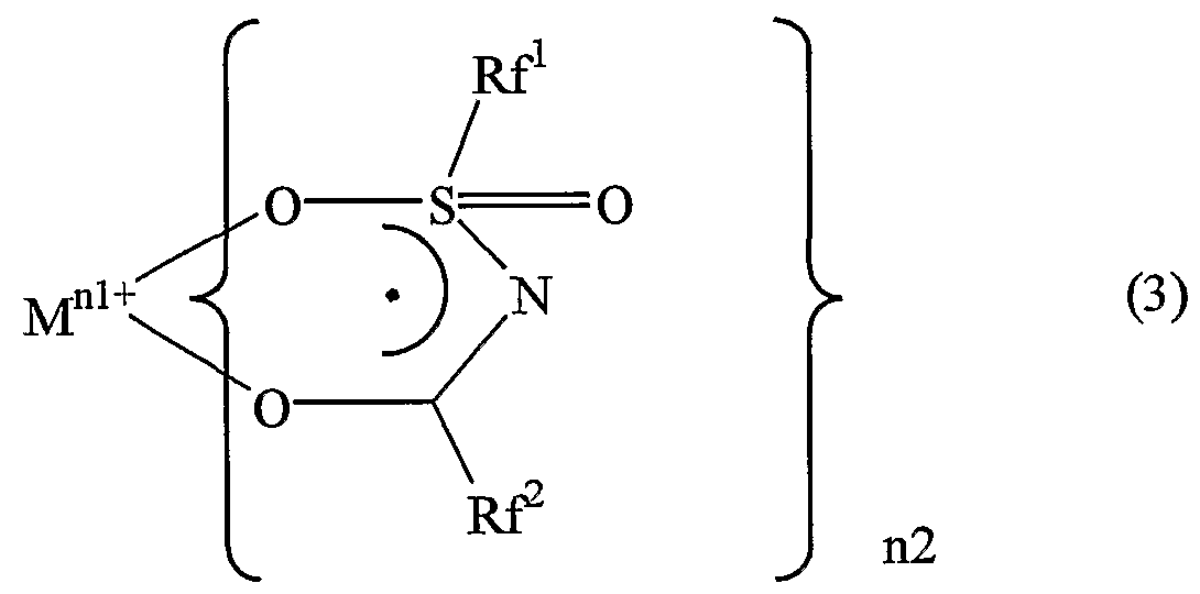


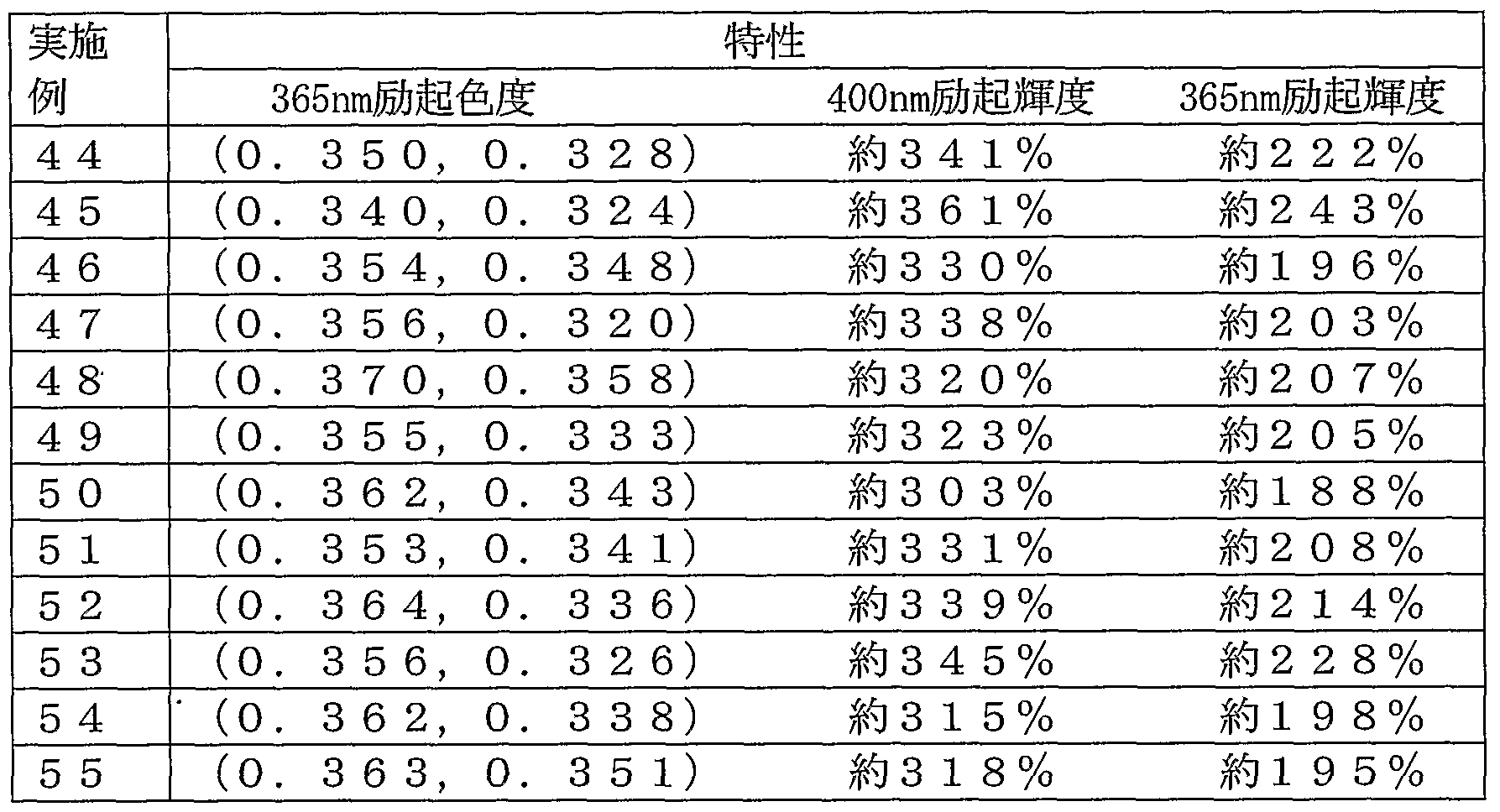


Claims
Priority Applications (5)
| Application Number | Priority Date | Filing Date | Title |
|---|---|---|---|
| EP06003714.0A EP1672707B1 (en) | 2001-04-20 | 2002-04-19 | Light emitting device |
| US10/475,314 US7091656B2 (en) | 2001-04-20 | 2002-04-19 | Light emitting device |
| JP2002584393A JP4048954B2 (ja) | 2001-04-20 | 2002-04-19 | 発光デバイス |
| EP02720511.1A EP1394864B1 (en) | 2001-04-20 | 2002-04-19 | Light emitting device |
| US11/384,548 US7247257B2 (en) | 2001-04-20 | 2006-03-21 | Light emitting device |
Applications Claiming Priority (8)
| Application Number | Priority Date | Filing Date | Title |
|---|---|---|---|
| JP2001-123457 | 2001-04-20 | ||
| JP2001123457 | 2001-04-20 | ||
| JP2001203240 | 2001-07-04 | ||
| JP2001-203240 | 2001-07-04 | ||
| JP2001288070 | 2001-09-21 | ||
| JP2001-288070 | 2001-09-21 | ||
| JP2001320201 | 2001-10-18 | ||
| JP2001-320201 | 2001-10-18 |
Related Child Applications (2)
| Application Number | Title | Priority Date | Filing Date |
|---|---|---|---|
| US10475314 A-371-Of-International | 2002-04-19 | ||
| US11/384,548 Division US7247257B2 (en) | 2001-04-20 | 2006-03-21 | Light emitting device |
Publications (1)
| Publication Number | Publication Date |
|---|---|
| WO2002086978A1 true WO2002086978A1 (fr) | 2002-10-31 |
Family
ID=27482226
Family Applications (1)
| Application Number | Title | Priority Date | Filing Date |
|---|---|---|---|
| PCT/JP2002/003901 WO2002086978A1 (fr) | 2001-04-20 | 2002-04-19 | Dispositif photoemetteur |
Country Status (6)
| Country | Link |
|---|---|
| US (1) | US7247257B2 (ja) |
| EP (2) | EP1672707B1 (ja) |
| JP (1) | JP4048954B2 (ja) |
| MY (1) | MY134305A (ja) |
| TW (1) | TW541722B (ja) |
| WO (1) | WO2002086978A1 (ja) |
Cited By (15)
| Publication number | Priority date | Publication date | Assignee | Title |
|---|---|---|---|---|
| JP2003069084A (ja) * | 2001-08-27 | 2003-03-07 | Toshiba Electronic Engineering Corp | 発光装置 |
| JP2004235546A (ja) * | 2003-01-31 | 2004-08-19 | Mitsubishi Chemicals Corp | 発光装置及びそれを用いた照明装置並びにディスプレイ |
| JP2004253747A (ja) * | 2002-02-27 | 2004-09-09 | Mitsubishi Chemicals Corp | 発光装置及びそれを用いた照明装置 |
| JP2005039264A (ja) * | 2003-06-30 | 2005-02-10 | Nichia Chem Ind Ltd | 半導体発光素子及びそれを用いた発光装置 |
| EP1507296A1 (en) * | 2003-08-12 | 2005-02-16 | Stanley Electric Co., Ltd. | Wavelength-converting LED |
| WO2005029596A1 (ja) * | 2003-09-18 | 2005-03-31 | Nichia Corporation | 発光装置 |
| JP2005093985A (ja) * | 2003-09-17 | 2005-04-07 | Nan Ya Plast Corp | 二次励起方式で白色光を産出する方法とその白色発光デバイス |
| WO2005097938A1 (ja) * | 2004-03-31 | 2005-10-20 | Nippon Electric Glass Co., Ltd. | 蛍光体及び発光ダイオード |
| JP2005330483A (ja) * | 2004-05-03 | 2005-12-02 | General Electric Co <Ge> | アルカリ土類金属及び13族金属の酸化物を含む蛍光体及び該蛍光体を組み込む光源 |
| JP2006024913A (ja) * | 2004-06-09 | 2006-01-26 | Showa Denko Kk | 窒化ガリウム系化合物半導体発光素子用透光性正極および発光素子 |
| US7357882B2 (en) * | 2002-02-15 | 2008-04-15 | Mitsubishi Chemical Corporation | Light emitting device and illuminator using the same |
| JP2010021578A (ja) * | 2002-02-27 | 2010-01-28 | Mitsubishi Chemicals Corp | 発光装置に用いる蛍光体 |
| RU2470413C2 (ru) * | 2007-05-25 | 2012-12-20 | ФИЛИПС ЛЬЮМИЛДЗ ЛАЙТИНГ КОМПАНИ, ЭлЭлСи | Устройство освещения с элементом преобразования длины волны, поддерживаемым посредством опорной конструкции, имеющей апертуру |
| US9431624B2 (en) | 2012-07-13 | 2016-08-30 | Panasonic Intellectual Property Management Co., Ltd. | Organic electroluminescent element |
| CN110959201A (zh) * | 2017-06-28 | 2020-04-03 | 京瓷株式会社 | 发光装置和照明装置 |
Families Citing this family (18)
| Publication number | Priority date | Publication date | Assignee | Title |
|---|---|---|---|---|
| US7229573B2 (en) | 2004-04-20 | 2007-06-12 | Gelcore, Llc | Ce3+ and Eu2+ doped phosphors for light generation |
| CN101032035A (zh) | 2004-09-28 | 2007-09-05 | 皇家飞利浦电子股份有限公司 | 具有改进转化层的发光器件 |
| WO2007081719A2 (en) | 2006-01-05 | 2007-07-19 | Illumitex, Inc. | Separate optical device for directing light from an led |
| WO2008042351A2 (en) * | 2006-10-02 | 2008-04-10 | Illumitex, Inc. | Led system and method |
| DE102007009820A1 (de) * | 2007-02-28 | 2008-09-04 | Osram Opto Semiconductors Gmbh | Optische Anordnung und optisches Verfahren |
| WO2008111504A1 (ja) * | 2007-03-12 | 2008-09-18 | Nichia Corporation | 高出力発光装置及びそれに用いるパッケージ |
| US20110182072A1 (en) * | 2007-06-29 | 2011-07-28 | Mitsubishi Chemical Corporation | Phosphor, production method of phosphor, phosphor-containing composition, and light emitting device |
| DE102008006990A1 (de) * | 2008-01-31 | 2009-08-06 | Osram Opto Semiconductors Gmbh | Hintergrundbeleuchtungseinheit für eine Hintergrundbeleuchtung eines Bildschirms und Bildschirmeinheit des Bildschirms |
| KR100903627B1 (ko) * | 2008-02-05 | 2009-06-18 | 삼성에스디아이 주식회사 | 디스플레이 장치용 형광체 조성물 |
| US7829358B2 (en) | 2008-02-08 | 2010-11-09 | Illumitex, Inc. | System and method for emitter layer shaping |
| DE102009018603B9 (de) | 2008-04-25 | 2021-01-14 | Samsung Electronics Co., Ltd. | Leuchtvorrichtung und Herstellungsverfahren derselben |
| KR101438826B1 (ko) * | 2008-06-23 | 2014-09-05 | 엘지이노텍 주식회사 | 발광장치 |
| US8410681B2 (en) * | 2008-06-30 | 2013-04-02 | Bridgelux, Inc. | Light emitting device having a refractory phosphor layer |
| TW201034256A (en) | 2008-12-11 | 2010-09-16 | Illumitex Inc | Systems and methods for packaging light-emitting diode devices |
| US8449128B2 (en) | 2009-08-20 | 2013-05-28 | Illumitex, Inc. | System and method for a lens and phosphor layer |
| US8585253B2 (en) | 2009-08-20 | 2013-11-19 | Illumitex, Inc. | System and method for color mixing lens array |
| DE102009050542A1 (de) * | 2009-10-23 | 2011-04-28 | Merck Patent Gmbh | Sm-aktivierte Aluminat- und Borat-Leuchtstoffe |
| DE102018117393A1 (de) * | 2018-07-18 | 2020-01-23 | Infineon Technologies Ag | Auflagetisch, auflagetischbaugruppe,verarbeitungsanordnung und verfahren dafür |
Citations (8)
| Publication number | Priority date | Publication date | Assignee | Title |
|---|---|---|---|---|
| US3513103A (en) * | 1967-12-12 | 1970-05-19 | Sylvania Electric Prod | Fluorescent phosphor |
| WO1997048138A2 (en) * | 1996-06-11 | 1997-12-18 | Philips Electronics N.V. | Visible light emitting devices including uv-light emitting diode and uv-excitable, visible light emitting phosphor, and method of producing such devices |
| JPH10275934A (ja) * | 1997-03-28 | 1998-10-13 | Rohm Co Ltd | 半導体発光素子 |
| JP2000031532A (ja) * | 1998-07-14 | 2000-01-28 | Toshiba Electronic Engineering Corp | 半導体発光装置 |
| US6051925A (en) * | 1997-03-03 | 2000-04-18 | U.S. Philips Corporation | Diode-addressed color display with molecular phosphor |
| JP2000183408A (ja) * | 1998-12-16 | 2000-06-30 | Toshiba Electronic Engineering Corp | 半導体発光装置 |
| JP2000230172A (ja) * | 1998-12-09 | 2000-08-22 | Sharp Corp | 蛍光部材及びそれを用いた発光素子 |
| JP2000347601A (ja) * | 1999-06-02 | 2000-12-15 | Toshiba Electronic Engineering Corp | 発光装置 |
Family Cites Families (29)
| Publication number | Priority date | Publication date | Assignee | Title |
|---|---|---|---|---|
| NL181470C (nl) * | 1977-08-23 | 1987-08-17 | Philips Nv | Lagedrukkwikdampontladingslamp. |
| FR2379160A1 (fr) * | 1977-01-28 | 1978-08-25 | Gen Electric | Lampe fluorescente perfectionnee |
| JPS5842590B2 (ja) * | 1977-08-30 | 1983-09-20 | 株式会社東芝 | けい光ランプ |
| US4426600A (en) * | 1977-09-06 | 1984-01-17 | Gte Products Corporation | Standard white fluorescent lamps employing blend |
| US4698548A (en) * | 1985-10-15 | 1987-10-06 | Gte Products Corporation | Lamp incorporating phosphor blend of calcium fluorophosphate and strontium halophosphate |
| JPH05152609A (ja) | 1991-11-25 | 1993-06-18 | Nichia Chem Ind Ltd | 発光ダイオード |
| JP3065494B2 (ja) * | 1994-12-02 | 2000-07-17 | 東芝ライテック株式会社 | 蛍光ランプおよびこれを用いたカラー液晶表示装置 |
| JPH09153645A (ja) | 1995-11-30 | 1997-06-10 | Toyoda Gosei Co Ltd | 3族窒化物半導体発光素子 |
| JP2927279B2 (ja) | 1996-07-29 | 1999-07-28 | 日亜化学工業株式会社 | 発光ダイオード |
| TW383508B (en) * | 1996-07-29 | 2000-03-01 | Nichia Kagaku Kogyo Kk | Light emitting device and display |
| TW385063U (en) | 1996-12-28 | 2000-03-11 | Shing Chen | New white light LED |
| DE59814117D1 (de) * | 1997-03-03 | 2007-12-20 | Philips Intellectual Property | Weisse lumineszenzdiode |
| WO1998040908A1 (fr) | 1997-03-10 | 1998-09-17 | Matsushita Electric Industrial Co., Ltd. | Lampe fluorescente |
| US6252254B1 (en) | 1998-02-06 | 2001-06-26 | General Electric Company | Light emitting device with phosphor composition |
| US6351069B1 (en) * | 1999-02-18 | 2002-02-26 | Lumileds Lighting, U.S., Llc | Red-deficiency-compensating phosphor LED |
| US6501100B1 (en) * | 2000-05-15 | 2002-12-31 | General Electric Company | White light emitting phosphor blend for LED devices |
| JP2002190622A (ja) | 2000-12-22 | 2002-07-05 | Sanken Electric Co Ltd | 発光ダイオード用透光性蛍光カバー |
| JP2002076434A (ja) | 2000-08-28 | 2002-03-15 | Toyoda Gosei Co Ltd | 発光装置 |
| AT410266B (de) | 2000-12-28 | 2003-03-25 | Tridonic Optoelectronics Gmbh | Lichtquelle mit einem lichtemittierenden element |
| JP2002280607A (ja) | 2001-01-10 | 2002-09-27 | Toyoda Gosei Co Ltd | 発光装置 |
| US7091656B2 (en) * | 2001-04-20 | 2006-08-15 | Nichia Corporation | Light emitting device |
| US6685852B2 (en) | 2001-04-27 | 2004-02-03 | General Electric Company | Phosphor blends for generating white light from near-UV/blue light-emitting devices |
| US6616862B2 (en) | 2001-05-21 | 2003-09-09 | General Electric Company | Yellow light-emitting halophosphate phosphors and light sources incorporating the same |
| DE20115914U1 (de) | 2001-09-27 | 2003-02-13 | Patent Treuhand Ges Fuer Elektrische Gluehlampen Mbh | Beleuchtungseinheit mit mindestens einer LED als Lichtquelle |
| US6924596B2 (en) | 2001-11-01 | 2005-08-02 | Nichia Corporation | Light emitting apparatus provided with fluorescent substance and semiconductor light emitting device, and method of manufacturing the same |
| JP3956972B2 (ja) | 2002-04-25 | 2007-08-08 | 日亜化学工業株式会社 | 蛍光物質を用いた発光装置 |
| US6809471B2 (en) | 2002-06-28 | 2004-10-26 | General Electric Company | Phosphors containing oxides of alkaline-earth and Group-IIIB metals and light sources incorporating the same |
| JP4389513B2 (ja) | 2003-08-08 | 2009-12-24 | 三菱化学株式会社 | 発光装置及び照明装置ならびに画像表示装置 |
| US7723740B2 (en) | 2003-09-18 | 2010-05-25 | Nichia Corporation | Light emitting device |
-
2002
- 2002-04-19 EP EP06003714.0A patent/EP1672707B1/en not_active Expired - Lifetime
- 2002-04-19 JP JP2002584393A patent/JP4048954B2/ja not_active Expired - Fee Related
- 2002-04-19 TW TW091108116A patent/TW541722B/zh not_active IP Right Cessation
- 2002-04-19 EP EP02720511.1A patent/EP1394864B1/en not_active Expired - Lifetime
- 2002-04-19 MY MYPI20021466A patent/MY134305A/en unknown
- 2002-04-19 WO PCT/JP2002/003901 patent/WO2002086978A1/ja active Application Filing
-
2006
- 2006-03-21 US US11/384,548 patent/US7247257B2/en not_active Expired - Lifetime
Patent Citations (8)
| Publication number | Priority date | Publication date | Assignee | Title |
|---|---|---|---|---|
| US3513103A (en) * | 1967-12-12 | 1970-05-19 | Sylvania Electric Prod | Fluorescent phosphor |
| WO1997048138A2 (en) * | 1996-06-11 | 1997-12-18 | Philips Electronics N.V. | Visible light emitting devices including uv-light emitting diode and uv-excitable, visible light emitting phosphor, and method of producing such devices |
| US6051925A (en) * | 1997-03-03 | 2000-04-18 | U.S. Philips Corporation | Diode-addressed color display with molecular phosphor |
| JPH10275934A (ja) * | 1997-03-28 | 1998-10-13 | Rohm Co Ltd | 半導体発光素子 |
| JP2000031532A (ja) * | 1998-07-14 | 2000-01-28 | Toshiba Electronic Engineering Corp | 半導体発光装置 |
| JP2000230172A (ja) * | 1998-12-09 | 2000-08-22 | Sharp Corp | 蛍光部材及びそれを用いた発光素子 |
| JP2000183408A (ja) * | 1998-12-16 | 2000-06-30 | Toshiba Electronic Engineering Corp | 半導体発光装置 |
| JP2000347601A (ja) * | 1999-06-02 | 2000-12-15 | Toshiba Electronic Engineering Corp | 発光装置 |
Non-Patent Citations (2)
| Title |
|---|
| PHOSPHOR RESEARCH SOCIETY, 25 December 1987, KEIKOTAI HANDBOOK, XP002955012 * |
| See also references of EP1394864A4 * |
Cited By (24)
| Publication number | Priority date | Publication date | Assignee | Title |
|---|---|---|---|---|
| JP2003069084A (ja) * | 2001-08-27 | 2003-03-07 | Toshiba Electronic Engineering Corp | 発光装置 |
| US7357882B2 (en) * | 2002-02-15 | 2008-04-15 | Mitsubishi Chemical Corporation | Light emitting device and illuminator using the same |
| JP2004253747A (ja) * | 2002-02-27 | 2004-09-09 | Mitsubishi Chemicals Corp | 発光装置及びそれを用いた照明装置 |
| JP2010021578A (ja) * | 2002-02-27 | 2010-01-28 | Mitsubishi Chemicals Corp | 発光装置に用いる蛍光体 |
| JP2004235546A (ja) * | 2003-01-31 | 2004-08-19 | Mitsubishi Chemicals Corp | 発光装置及びそれを用いた照明装置並びにディスプレイ |
| JP2005039264A (ja) * | 2003-06-30 | 2005-02-10 | Nichia Chem Ind Ltd | 半導体発光素子及びそれを用いた発光装置 |
| JP4572604B2 (ja) * | 2003-06-30 | 2010-11-04 | 日亜化学工業株式会社 | 半導体発光素子及びそれを用いた発光装置 |
| US7309881B2 (en) | 2003-08-12 | 2007-12-18 | Stanley Electric Co., Ltd. | Wavelength-converting LED |
| EP1507296A1 (en) * | 2003-08-12 | 2005-02-16 | Stanley Electric Co., Ltd. | Wavelength-converting LED |
| CN100358164C (zh) * | 2003-08-12 | 2007-12-26 | 斯坦雷电气株式会社 | 波长变换型发光二极管 |
| JP2005093985A (ja) * | 2003-09-17 | 2005-04-07 | Nan Ya Plast Corp | 二次励起方式で白色光を産出する方法とその白色発光デバイス |
| WO2005029596A1 (ja) * | 2003-09-18 | 2005-03-31 | Nichia Corporation | 発光装置 |
| CN100428508C (zh) * | 2003-09-18 | 2008-10-22 | 日亚化学工业株式会社 | 发光装置 |
| US7723740B2 (en) | 2003-09-18 | 2010-05-25 | Nichia Corporation | Light emitting device |
| EP1670070A1 (en) * | 2003-09-18 | 2006-06-14 | Nichia Corporation | Light-emitting device |
| EP1670070A4 (en) * | 2003-09-18 | 2011-08-17 | Nichia Corp | LIGHT-EMITTING DEVICE |
| KR101065522B1 (ko) | 2003-09-18 | 2011-09-19 | 니치아 카가쿠 고교 가부시키가이샤 | 발광 장치 |
| WO2005097938A1 (ja) * | 2004-03-31 | 2005-10-20 | Nippon Electric Glass Co., Ltd. | 蛍光体及び発光ダイオード |
| JP2005330483A (ja) * | 2004-05-03 | 2005-12-02 | General Electric Co <Ge> | アルカリ土類金属及び13族金属の酸化物を含む蛍光体及び該蛍光体を組み込む光源 |
| JP2006024913A (ja) * | 2004-06-09 | 2006-01-26 | Showa Denko Kk | 窒化ガリウム系化合物半導体発光素子用透光性正極および発光素子 |
| RU2470413C2 (ru) * | 2007-05-25 | 2012-12-20 | ФИЛИПС ЛЬЮМИЛДЗ ЛАЙТИНГ КОМПАНИ, ЭлЭлСи | Устройство освещения с элементом преобразования длины волны, поддерживаемым посредством опорной конструкции, имеющей апертуру |
| US9431624B2 (en) | 2012-07-13 | 2016-08-30 | Panasonic Intellectual Property Management Co., Ltd. | Organic electroluminescent element |
| CN110959201A (zh) * | 2017-06-28 | 2020-04-03 | 京瓷株式会社 | 发光装置和照明装置 |
| CN110959201B (zh) * | 2017-06-28 | 2023-05-09 | 京瓷株式会社 | 发光装置和照明装置 |
Also Published As
| Publication number | Publication date |
|---|---|
| JPWO2002086978A1 (ja) | 2004-08-12 |
| EP1672707A2 (en) | 2006-06-21 |
| EP1394864A4 (en) | 2010-09-29 |
| EP1394864B1 (en) | 2016-08-03 |
| EP1672707B1 (en) | 2019-07-31 |
| EP1672707A3 (en) | 2008-02-20 |
| JP4048954B2 (ja) | 2008-02-20 |
| MY134305A (en) | 2007-12-31 |
| EP1394864A1 (en) | 2004-03-03 |
| US20060163999A1 (en) | 2006-07-27 |
| US7247257B2 (en) | 2007-07-24 |
| TW541722B (en) | 2003-07-11 |
Similar Documents
| Publication | Publication Date | Title |
|---|---|---|
| JP4048954B2 (ja) | 発光デバイス | |
| JP4991026B2 (ja) | 発光装置 | |
| JP3956972B2 (ja) | 蛍光物質を用いた発光装置 | |
| EP1837386B1 (en) | Nitride phosphor, method for producing same and light-emitting device using nitride phosphor | |
| JP4244653B2 (ja) | シリコンナイトライド系蛍光体及びそれを用いた発光装置 | |
| JP5151002B2 (ja) | 発光装置 | |
| US7733002B2 (en) | Semiconductor light emitting device provided with an alkaline earth metal boric halide phosphor for luminescence conversion | |
| US20040095063A1 (en) | Light emitting device | |
| JP5066786B2 (ja) | 窒化物蛍光体及びそれを用いた発光装置 | |
| JP4222059B2 (ja) | 発光装置 | |
| JP4892861B2 (ja) | 窒化物蛍光体及びそれを用いた発光装置 | |
| JP4214768B2 (ja) | 窒化物蛍光体及びそれを用いた発光装置 | |
| JP4151284B2 (ja) | 窒化物半導体発光素子及び発光装置並びにそれらの製造方法 | |
| JP2002324915A (ja) | 集積型窒化物半導体発光素子 | |
| JP4187033B2 (ja) | 発光装置 | |
| JP4218328B2 (ja) | 窒化物蛍光体及びそれを用いた発光装置 | |
| JP4363215B2 (ja) | アルカリ土類金属アルミン酸塩蛍光体及びそれを用いた発光装置 | |
| JP4215046B2 (ja) | 窒化物蛍光体及びそれを用いた発光装置 | |
| JP4991027B2 (ja) | オキシ窒化物蛍光体及びそれを用いた発光装置 | |
| JP4096977B2 (ja) | 白色発光装置、発光デバイス及び蛍光物質 | |
| JP4215045B2 (ja) | 窒化物蛍光体及びそれを用いた発光装置 | |
| JP4363217B2 (ja) | アルカリ土類金属ホウ酸塩蛍光体及びそれを用いた発光装置 |
Legal Events
| Date | Code | Title | Description |
|---|---|---|---|
| AK | Designated states |
Kind code of ref document: A1 Designated state(s): AE AG AL AM AT AU AZ BA BB BG BR BY BZ CA CH CN CO CR CU CZ DE DK DM DZ EC EE ES FI GB GD GE GH GM HR HU ID IL IN IS JP KE KG KR KZ LC LK LR LS LT LU LV MA MD MG MK MN MW MX MZ NO NZ OM PH PL PT RO RU SD SE SG SI SK SL TJ TM TN TR TT TZ UA UG US UZ VN YU ZA ZM ZW |
|
| AL | Designated countries for regional patents |
Kind code of ref document: A1 Designated state(s): GH GM KE LS MW MZ SD SL SZ TZ UG ZM ZW AM AZ BY KG KZ MD RU TJ TM AT BE CH CY DE DK ES FI FR GB GR IE IT LU MC NL PT SE TR BF BJ CF CG CI CM GA GN GQ GW ML MR NE SN TD TG |
|
| 121 | Ep: the epo has been informed by wipo that ep was designated in this application | ||
| DFPE | Request for preliminary examination filed prior to expiration of 19th month from priority date (pct application filed before 20040101) | ||
| WWE | Wipo information: entry into national phase |
Ref document number: 2002584393 Country of ref document: JP |
|
| WWE | Wipo information: entry into national phase |
Ref document number: 10475314 Country of ref document: US |
|
| REEP | Request for entry into the european phase |
Ref document number: 2002720511 Country of ref document: EP |
|
| WWE | Wipo information: entry into national phase |
Ref document number: 2002720511 Country of ref document: EP |
|
| WWP | Wipo information: published in national office |
Ref document number: 2002720511 Country of ref document: EP |
|
| REG | Reference to national code |
Ref country code: DE Ref legal event code: 8642 |