US9934736B2 - Liquid crystal display and method for driving the same - Google Patents
Liquid crystal display and method for driving the same Download PDFInfo
- Publication number
- US9934736B2 US9934736B2 US14/328,240 US201414328240A US9934736B2 US 9934736 B2 US9934736 B2 US 9934736B2 US 201414328240 A US201414328240 A US 201414328240A US 9934736 B2 US9934736 B2 US 9934736B2
- Authority
- US
- United States
- Prior art keywords
- subpixels
- data
- voltage
- data lines
- polarity
- Prior art date
- Legal status (The legal status is an assumption and is not a legal conclusion. Google has not performed a legal analysis and makes no representation as to the accuracy of the status listed.)
- Active, expires
Links
Images


Classifications
-
- G—PHYSICS
- G02—OPTICS
- G02F—OPTICAL DEVICES OR ARRANGEMENTS FOR THE CONTROL OF LIGHT BY MODIFICATION OF THE OPTICAL PROPERTIES OF THE MEDIA OF THE ELEMENTS INVOLVED THEREIN; NON-LINEAR OPTICS; FREQUENCY-CHANGING OF LIGHT; OPTICAL LOGIC ELEMENTS; OPTICAL ANALOGUE/DIGITAL CONVERTERS
- G02F1/00—Devices or arrangements for the control of the intensity, colour, phase, polarisation or direction of light arriving from an independent light source, e.g. switching, gating or modulating; Non-linear optics
- G02F1/01—Devices or arrangements for the control of the intensity, colour, phase, polarisation or direction of light arriving from an independent light source, e.g. switching, gating or modulating; Non-linear optics for the control of the intensity, phase, polarisation or colour
- G02F1/13—Devices or arrangements for the control of the intensity, colour, phase, polarisation or direction of light arriving from an independent light source, e.g. switching, gating or modulating; Non-linear optics for the control of the intensity, phase, polarisation or colour based on liquid crystals, e.g. single liquid crystal display cells
- G02F1/133—Constructional arrangements; Operation of liquid crystal cells; Circuit arrangements
-
- G—PHYSICS
- G09—EDUCATION; CRYPTOGRAPHY; DISPLAY; ADVERTISING; SEALS
- G09G—ARRANGEMENTS OR CIRCUITS FOR CONTROL OF INDICATING DEVICES USING STATIC MEANS TO PRESENT VARIABLE INFORMATION
- G09G3/00—Control arrangements or circuits, of interest only in connection with visual indicators other than cathode-ray tubes
- G09G3/20—Control arrangements or circuits, of interest only in connection with visual indicators other than cathode-ray tubes for presentation of an assembly of a number of characters, e.g. a page, by composing the assembly by combination of individual elements arranged in a matrix no fixed position being assigned to or needed to be assigned to the individual characters or partial characters
- G09G3/34—Control arrangements or circuits, of interest only in connection with visual indicators other than cathode-ray tubes for presentation of an assembly of a number of characters, e.g. a page, by composing the assembly by combination of individual elements arranged in a matrix no fixed position being assigned to or needed to be assigned to the individual characters or partial characters by control of light from an independent source
- G09G3/36—Control arrangements or circuits, of interest only in connection with visual indicators other than cathode-ray tubes for presentation of an assembly of a number of characters, e.g. a page, by composing the assembly by combination of individual elements arranged in a matrix no fixed position being assigned to or needed to be assigned to the individual characters or partial characters by control of light from an independent source using liquid crystals
- G09G3/3611—Control of matrices with row and column drivers
- G09G3/3614—Control of polarity reversal in general
-
- G—PHYSICS
- G09—EDUCATION; CRYPTOGRAPHY; DISPLAY; ADVERTISING; SEALS
- G09G—ARRANGEMENTS OR CIRCUITS FOR CONTROL OF INDICATING DEVICES USING STATIC MEANS TO PRESENT VARIABLE INFORMATION
- G09G3/00—Control arrangements or circuits, of interest only in connection with visual indicators other than cathode-ray tubes
- G09G3/20—Control arrangements or circuits, of interest only in connection with visual indicators other than cathode-ray tubes for presentation of an assembly of a number of characters, e.g. a page, by composing the assembly by combination of individual elements arranged in a matrix no fixed position being assigned to or needed to be assigned to the individual characters or partial characters
- G09G3/34—Control arrangements or circuits, of interest only in connection with visual indicators other than cathode-ray tubes for presentation of an assembly of a number of characters, e.g. a page, by composing the assembly by combination of individual elements arranged in a matrix no fixed position being assigned to or needed to be assigned to the individual characters or partial characters by control of light from an independent source
- G09G3/36—Control arrangements or circuits, of interest only in connection with visual indicators other than cathode-ray tubes for presentation of an assembly of a number of characters, e.g. a page, by composing the assembly by combination of individual elements arranged in a matrix no fixed position being assigned to or needed to be assigned to the individual characters or partial characters by control of light from an independent source using liquid crystals
- G09G3/3611—Control of matrices with row and column drivers
-
- G—PHYSICS
- G02—OPTICS
- G02F—OPTICAL DEVICES OR ARRANGEMENTS FOR THE CONTROL OF LIGHT BY MODIFICATION OF THE OPTICAL PROPERTIES OF THE MEDIA OF THE ELEMENTS INVOLVED THEREIN; NON-LINEAR OPTICS; FREQUENCY-CHANGING OF LIGHT; OPTICAL LOGIC ELEMENTS; OPTICAL ANALOGUE/DIGITAL CONVERTERS
- G02F1/00—Devices or arrangements for the control of the intensity, colour, phase, polarisation or direction of light arriving from an independent light source, e.g. switching, gating or modulating; Non-linear optics
- G02F1/01—Devices or arrangements for the control of the intensity, colour, phase, polarisation or direction of light arriving from an independent light source, e.g. switching, gating or modulating; Non-linear optics for the control of the intensity, phase, polarisation or colour
- G02F1/13—Devices or arrangements for the control of the intensity, colour, phase, polarisation or direction of light arriving from an independent light source, e.g. switching, gating or modulating; Non-linear optics for the control of the intensity, phase, polarisation or colour based on liquid crystals, e.g. single liquid crystal display cells
- G02F1/133—Constructional arrangements; Operation of liquid crystal cells; Circuit arrangements
- G02F1/136—Liquid crystal cells structurally associated with a semi-conducting layer or substrate, e.g. cells forming part of an integrated circuit
- G02F1/1362—Active matrix addressed cells
-
- G—PHYSICS
- G09—EDUCATION; CRYPTOGRAPHY; DISPLAY; ADVERTISING; SEALS
- G09G—ARRANGEMENTS OR CIRCUITS FOR CONTROL OF INDICATING DEVICES USING STATIC MEANS TO PRESENT VARIABLE INFORMATION
- G09G3/00—Control arrangements or circuits, of interest only in connection with visual indicators other than cathode-ray tubes
- G09G3/20—Control arrangements or circuits, of interest only in connection with visual indicators other than cathode-ray tubes for presentation of an assembly of a number of characters, e.g. a page, by composing the assembly by combination of individual elements arranged in a matrix no fixed position being assigned to or needed to be assigned to the individual characters or partial characters
- G09G3/34—Control arrangements or circuits, of interest only in connection with visual indicators other than cathode-ray tubes for presentation of an assembly of a number of characters, e.g. a page, by composing the assembly by combination of individual elements arranged in a matrix no fixed position being assigned to or needed to be assigned to the individual characters or partial characters by control of light from an independent source
- G09G3/36—Control arrangements or circuits, of interest only in connection with visual indicators other than cathode-ray tubes for presentation of an assembly of a number of characters, e.g. a page, by composing the assembly by combination of individual elements arranged in a matrix no fixed position being assigned to or needed to be assigned to the individual characters or partial characters by control of light from an independent source using liquid crystals
-
- G—PHYSICS
- G09—EDUCATION; CRYPTOGRAPHY; DISPLAY; ADVERTISING; SEALS
- G09G—ARRANGEMENTS OR CIRCUITS FOR CONTROL OF INDICATING DEVICES USING STATIC MEANS TO PRESENT VARIABLE INFORMATION
- G09G2310/00—Command of the display device
- G09G2310/06—Details of flat display driving waveforms
- G09G2310/065—Waveforms comprising zero voltage phase or pause
-
- G—PHYSICS
- G09—EDUCATION; CRYPTOGRAPHY; DISPLAY; ADVERTISING; SEALS
- G09G—ARRANGEMENTS OR CIRCUITS FOR CONTROL OF INDICATING DEVICES USING STATIC MEANS TO PRESENT VARIABLE INFORMATION
- G09G2320/00—Control of display operating conditions
- G09G2320/02—Improving the quality of display appearance
- G09G2320/0204—Compensation of DC component across the pixels in flat panels
-
- G—PHYSICS
- G09—EDUCATION; CRYPTOGRAPHY; DISPLAY; ADVERTISING; SEALS
- G09G—ARRANGEMENTS OR CIRCUITS FOR CONTROL OF INDICATING DEVICES USING STATIC MEANS TO PRESENT VARIABLE INFORMATION
- G09G3/00—Control arrangements or circuits, of interest only in connection with visual indicators other than cathode-ray tubes
- G09G3/20—Control arrangements or circuits, of interest only in connection with visual indicators other than cathode-ray tubes for presentation of an assembly of a number of characters, e.g. a page, by composing the assembly by combination of individual elements arranged in a matrix no fixed position being assigned to or needed to be assigned to the individual characters or partial characters
- G09G3/34—Control arrangements or circuits, of interest only in connection with visual indicators other than cathode-ray tubes for presentation of an assembly of a number of characters, e.g. a page, by composing the assembly by combination of individual elements arranged in a matrix no fixed position being assigned to or needed to be assigned to the individual characters or partial characters by control of light from an independent source
- G09G3/36—Control arrangements or circuits, of interest only in connection with visual indicators other than cathode-ray tubes for presentation of an assembly of a number of characters, e.g. a page, by composing the assembly by combination of individual elements arranged in a matrix no fixed position being assigned to or needed to be assigned to the individual characters or partial characters by control of light from an independent source using liquid crystals
- G09G3/3607—Control arrangements or circuits, of interest only in connection with visual indicators other than cathode-ray tubes for presentation of an assembly of a number of characters, e.g. a page, by composing the assembly by combination of individual elements arranged in a matrix no fixed position being assigned to or needed to be assigned to the individual characters or partial characters by control of light from an independent source using liquid crystals for displaying colours or for displaying grey scales with a specific pixel layout, e.g. using sub-pixels
Definitions
- Exemplary embodiments of the present invention relate to a liquid crystal display, and a method for driving the same.
- a liquid crystal display is one of the flat panel displays which have recently been widely used.
- An LCD generates an electric field by applying different potentials to a pixel electrode and a common electrode of a liquid crystal display panel so as to change an orientation of liquid crystal molecules and control light transmittance based on the changed orientation of the liquid crystal molecules, thereby displaying an image.
- Exemplary embodiments of the present invention provide a liquid crystal display having excellent display quality, and a method for driving the same.
- Exemplary embodiments of the present invention also provide a polarity disposition preventing polarity biasing of a data voltage from occurring in a liquid crystal display having a pixel which is formed of an even number of subpixels.
- An exemplary embodiment of the present invention discloses a liquid crystal display, including: gate lines arranged in a row direction; data lines arranged in a column direction; and subpixels arranged in basic units of eight subpixels. Each subpixel is connected to one of the gate lines and one of the data lines, and the subpixels are continuously arranged along a row.
- polarities between adjacent subpixels from a first subpixel to a fourth subpixel along the row may be opposite to each other
- polarities between adjacent subpixels from a fifth subpixel to an eighth subpixel along the row may be opposite to each other
- polarities of the fourth subpixel and the fifth subpixel may be the same as each other.
- An exemplary embodiment of the present invention also discloses a liquid crystal display, including: gate lines arranged in a row direction; data lines arranged in a column direction; and subpixels arranged in basic units of four subpixels. Each subpixel is connected to one of the gate lines and one of the data lines, and the subpixels are continuously arranged along a row. In the basic units, each two subpixels along the row may have opposite polarities. The subpixels which are present in one of the two columns adjacent to each other may have the same polarity along the column, and the subpixels which are present in the other column may have an opposite polarity between the adjacent subpixels along the column.
- An exemplary embodiment of the present invention also discloses a liquid crystal display, including: gate lines arranged in a row direction; data lines arranged in a column direction; and subpixels arranged in basic units of eight subpixels. Each subpixel is connected to one of the gate lines and one of the data lines, and the subpixels are continuously arranged along a row.
- the first to fourth subpixels may have an opposed polarity between adjacent subpixels
- the fifth to eighth subpixels may have an opposed polarity between the adjacent subpixels
- the fourth subpixel and the fifth subpixel may have the same polarity.
- subpixels of first to third columns and fifth to seventh columns may have an opposed polarity between the adjacent subpixels in each repetitive unit of three subpixels, and subpixels of the fourth column and the eighth column may have an opposite polarity for each three subpixels.
- An exemplary embodiment of the present invention also discloses a liquid crystal display, including: gate lines arranged in a row direction; data lines arranged in a column direction; and subpixels arranged in basic units of eight subpixels. Each subpixel is connected to one of the gate lines and one of the data lines, and the subpixels are continuously arranged along a row.
- first to fourth subpixels may have the same polarity
- fifth to eighth subpixels may have polarities opposite to those of the first to fourth subpixels.
- subpixels of first to third columns and fifth to seventh columns may have an opposed polarity for each repetitive unit of three subpixels
- subpixels of a fourth column and an eighth column may have an opposed polarity between the adjacent subpixels in each repetitive unit.
- An exemplary embodiment of the present invention also discloses a liquid crystal display, including: gate lines arranged in a row direction; data lines arranged in a column direction; and subpixels arranged in basic units of four subpixels. Each subpixel is connected to one of the gate lines and one of the data lines, and the subpixels are continuously arranged along a row. In the basic units, each two subpixels along the row may have opposite polarities. In the column direction, the subpixels which are present in one of the two columns adjacent to each other may have the same polarity, and the subpixels which are present in the other column may have an opposite polarity for each two subpixels.
- An exemplary embodiment of the present invention also discloses a liquid crystal display, including: gate lines arranged in a row direction; data lines arranged in a column direction; and subpixels arranged in basic units of six subpixels. Each of the subpixels is connected to one of the gate lines and one of the data lines, and the subpixels are continuously arranged along a row. A polarity may be opposed for each three subpixels in each basic unit along the row.
- An exemplary embodiment of the present invention also discloses a method for driving a liquid crystal display including subpixels arranged in a matrix which are respectively connected to gate lines arranged in a row direction and data lines arranged in a column direction.
- a data driver may apply a data voltage having an opposite polarity between adjacent subpixels in the row direction to data lines connected to first to fourth subpixels in the row direction; apply data voltages having an opposite polarity between adjacent subpixels in the row direction to data lines connected to fifth to eighth subpixel in the row direction; and apply data voltages having the same polarity to the data lines connected to the fourth and fifth subpixels in the row direction.
- FIG. 1 is a block diagram of a liquid display device according to an exemplary embodiment of the present invention.
- FIG. 2 is an equivalent circuit diagram of one subpixel in the liquid display device according to an exemplary embodiment of the present invention.
- FIG. 3 to FIG. 8 are diagrams illustrating a polarity disposition and an inversion driving of the liquid crystal display according to a first exemplary embodiment of the present invention.
- FIG. 9 to FIG. 11 are diagrams illustrating an example of a data voltage applied to a data line in the liquid crystal display according to the first exemplary embodiment of the present invention.
- FIG. 12 to FIG. 17 are diagrams illustrating a polarity disposition and an inversion driving of the liquid crystal display according to a second exemplary embodiment of the present invention.
- FIG. 18 to FIG. 20 are diagrams illustrating an example of a data voltage applied to a data line in the liquid crystal display according to the second exemplary embodiment of the present invention.
- FIG. 21 to FIG. 26 are diagrams illustrating polarity dispositions of liquid crystal displays according to other exemplary embodiments of the present invention.
- FIG. 27 and FIG. 28 are diagrams illustrating an example of a polarity disposition of the liquid crystal display in which polarity biasing of the data voltage occurs and the data voltage applied to a data line.
- a liquid crystal display and a method for driving the same according to an exemplary embodiment of the present invention will be described in detail with reference to FIGS. 1 to 2 .
- FIG. 1 is a block diagram of a liquid display device according to an exemplary embodiment of the present invention
- FIG. 2 is an equivalent circuit diagram of one subpixel in the liquid display device.
- a liquid crystal display 1 includes a liquid crystal display panel 300 which displays an image, a gate driver 400 , a data driver 500 , and a signal controller 600 .
- FIG. 1 also illustrates a graphics processor 10 , which is located outside the liquid crystal display 1 .
- the graphics processor 10 provides image signals R, G, and B, and a control signal CONT to the signal controller 600 of the liquid crystal display 1 .
- the control signal CONT includes a horizontal synchronization signal, a vertical synchronization signal, a clock signal, and a data enable signal, and the like.
- the image signals R, G, and B, and the control signal CONT may be transmitted to the signal controller 600 in, for example, a low voltage differential signaling (LVDS) scheme.
- LVDS low voltage differential signaling
- the liquid crystal display panel 300 includes lower and upper panels 100 and 200 which face each other, and a liquid crystal layer 3 disposed therebetween.
- the liquid crystal display panel 300 includes gate lines G 1 to Gn and data lines D 1 to Dm.
- the gate lines G 1 to Gn extend approximately in a horizontal (row) direction
- the data lines D 1 to Dm extend approximately in a vertical (column) direction, while being insulated from, and intersecting with, the gate lines G 1 to Gn.
- a single gate line and a single data line are connected to a single subpixel SPX.
- the subpixels SPX are arranged in a matrix, in which each subpixel SPX may include a thin film transistor Q, a liquid crystal capacitor Clc, and a sustain capacitor Cst.
- a pixel PX which is a minimum unit of an image, is formed of subpixels SPX, to which luminance may be independently assigned, such that the subpixels SPX are combined to be able to display colors and luminance.
- one pixel PX may be formed of three subpixels SPX representing red, green, and blue, which are three primary colors of light.
- the single pixel PX may also be formed of even-numbered subpixels SPX.
- the pixel PX may be formed of four subpixels SPX, each of which represents red, green, blue, and white.
- the single pixel PX may be formed of two subpixels SPX, each of which represents red and green, or blue and green, and such a scheme of forming the pixel PX is a so-called pentile scheme.
- a control terminal of the thin film transistor Q may be connected to one gate line Gi, an input terminal of the thin film transistor Q may be connected to one data line Dj, and an output terminal of the thin film transistor Q may be connected to a pixel electrode 191 , which is one terminal of the liquid crystal capacitor Clc, and one terminal of the sustain capacitor Cst.
- the other terminal of the liquid crystal capacitor Clc may be connected to a common electrode 270 , and a sustain voltage may be applied to the other terminal of the sustain capacitor Cst.
- both the pixel electrode 191 and the common electrode 270 may be formed on the lower panel 100 .
- the signal controller 600 receives input image signals R, G, and B and the control signal CONT, that is, the horizontal synchronizing signal, the vertical synchronization signal, the clock signal, the data enable signal, and the like, from the external graphic processor 10 .
- the signal controller 600 processes the image signals R, G, and B to be suitable for operating conditions of the liquid crystal display panel 300 based on the image signals R, G, and B and the control signal CONT, and then generates and outputs an image data DAT, a gate control signal CONT 1 , a data control signal CONT 2 , and the clock signal.
- the gate control signal CONT 1 includes a start pulse vertical signal, which instructs a start pulse, and a clock pulse vertical signal, which is a reference of generating a gate-on voltage. An output period of the start pulse vertical signal coincides with one frame or a refresh rate.
- the gate control signal CONT 1 may further include an output enable signal, which limits a sustain time of the gate-on voltage.
- the data control signal CONT 2 includes a start pulse horizontal signal, which instructs a transmission start of the image data DAT for the subpixel SPX of one row, a load signal, which instructs application of the corresponding data voltage to data lines D 1 to Dm, and the like.
- the data control signal CONT 2 may further include an inversion signal, which inverts a polarity of the data voltage with respect to a common voltage Vcom
- the gate lines G 1 to Gn of the liquid crystal display panel 300 are connected to the gate driver 400 , and the gate-on voltage is sequentially applied to the gate lines G 1 to Gn, depending on the gate control signal CONT 1 applied from the signal controller 600 , and a gate-off voltage is applied to the gate lines G 1 to Gn in a period in which the gate-on voltage is not applied.
- the data lines D 1 to Dm of the liquid crystal display panel 300 are connected to the data driver 500 , and the data driver 500 receives the data control signal CONT 2 and the image data DAT from the signal controller 600 .
- the data driver 500 converts the image data DAT into the data voltage using a gray voltage generated from a gray voltage generator (not illustrated), and transmits the data voltage to the data lines D 1 to Dm.
- the data voltage includes the data voltage having both a positive polarity and a negative polarity based on the common voltage (hereinafter, simply referred to as “positive data voltage” or “negative data voltage”).
- the positive data voltage and the negative data voltage are alternately applied based on a frame, a row, and/or a column, and thus, are driven in an inverted manner. Therefore, the inversion driving may be classified into types, such as a frame inversion, a column inversion, a row inversion (or line inversion), or a dot inversion, and the inversion may also be implemented in even a more complex manner.
- FIGS. 3 to 8 are diagrams illustrating polarity disposition and inversion driving of the liquid crystal display according to a first exemplary embodiment of the present invention.
- long vertical lines represent data lines that are arranged substantially in parallel with each other, and a rectangle represents a subpixel SPX.
- Short horizontal lines represent connections between the data line and the subpixel SPX.
- a positive (+) or a negative ( ⁇ ) within the rectangle represents the polarity (hereinafter, referred to as “polarity of subpixel SPX”) of the data voltage which is applied to each of the subpixels SPX at a specific time.
- the letters “a”, “b”, “c”, and “d” represent colors that are represented by each of the subpixels SPX. The same rule applies to the following drawings.
- FIG. 3 illustrates the polarity disposition in an n-th frame in the liquid crystal display
- FIG. 4 illustrates the polarity disposition in an n+1-th frame.
- All colors of “a”, “b”, “c”, and “d”, which are colors represented by each of the subpixels SPX, may be different; a pair of colors among these colors may be the same (for example, the colors “a” and “c” may be the same); or two pairs of colors may also be the same (For example, the colors of “a” and “c” may be the same, and the colors of “b” and “d” may be the same).
- four subpixels SPX of the colors of “a”, “b”, “c”, and “d” may form one pixel PX
- two subpixels SPX of the colors of “a” and “b” or two subpixels SPX of the colors of “c” and “d” may form one pixel PX.
- an exemplary embodiment of the present invention will be described in detail based on, by way of example, the case in which all the colors of “a”, “b”, “c”, and “d” are different, and four subpixels SPX form one pixel PX.
- the data lines are all connected to the subpixels SPX, which are located to the right of the data lines in FIGS. 3 and 4 .
- the data lines D 1 , D 2 , . . . Dm may all be connected to the subpixels SPX that are located to the right thereof, but any data line may instead be connected to the subpixels SPX that are located to the left thereof.
- a positive (+) data voltage is applied to first, third, sixth, and eighth data lines D 1 , D 3 , D 6 , and D 8
- a negative ( ⁇ ) data voltage is applied to second, fourth, fifth, and seventh data lines D 2 , D 4 , D 5 , and D 7
- the negative ( ⁇ ) data voltage is applied to first, third, sixth, and eighth data lines D 1 , D 3 , D 6 , and D 8
- the positive (+) data voltage is applied to second, fourth, fifth, and seventh data lines D 2 , D 4 , D 5 , and D 7 .
- the application of the data voltage having different polarities depending on the data line is repeated based on eight data lines. That is, the data voltage of positive (+), negative ( ⁇ ), positive (+), negative ( ⁇ ), negative ( ⁇ ), positive (+), negative ( ⁇ ), and positive (+) is repeatedly applied from the left data line to each data line. Therefore, the polarity of the data voltage applied to the first to eighth data lines D 1 to D 8 may also be similarly applied to ninth to sixteenth data lines D 9 to D 16 .
- the data driver 500 applies the data voltage having a polarity inverted for each frame to each data line so as to meet the foregoing polarity.
- the subpixels SPX that are located in the first to fourth columns have inverted polarity between the adjacent subpixels
- the subpixels SPX that are located in the fifth to eighth columns have inverted polarity between the adjacent subpixels SPX, but polarities of the subpixels SPX that are located in the fifth to eighth columns are opposite to those of the subpixels SPX that are located in the first to fourth columns, respectively.
- the array of first to eighth subpixels SPX configure a basic unit in which polarities are repeated in a row direction. That is, the polarities of the array of ninth to sixteenth subpixels SPX are sequentially the same as those of the array of first to eighth subpixel SPX.
- the number of positive (+) subpixels is the same as the number of negative ( ⁇ ) subpixels for each color.
- the positive (+) subpixel and the negative ( ⁇ ) subpixel are alternately disposed in the row direction for each color.
- the subpixel of color “a” in the two basic units the subpixel of color “a” is located at each four subpixels one-by-one, and the polarity thereof is positive (+), negative ( ⁇ ), positive (+), and negative ( ⁇ ) from the left. Therefore, because the positive polarity and the negative polarity are evenly mixed, the deterioration in display quality resulting from the difference in luminance, which may be present between the polarities, does not occur.
- the number of positive (+) subpixels is the same as the number of negative ( ⁇ ) subpixels for each color, and the positive (+) subpixel and the negative ( ⁇ ) subpixel are alternately disposed in the row direction for each color. Therefore, because the difference in luminance (for example, even though the data voltage having the same level is applied, the luminance may be different depending on the polarity) between the frames due to polarity mismatching is not present, flicker does not occur.
- the subpixels which are present in each subpixel array are respectively connected to the same data line.
- a difference in luminance resulting from a characteristic deviation such as a capacitance Cgs between a gate and a source of the thin film transistor, which may occur between subpixels connected to different data lines does not occur.
- FIGS. 5 and 6 illustrate the polarity dispositions of the n-th frame and the n+1-th frame at the time of displaying only one color.
- the case in which the “a” is red corresponds to the case of displaying a red screen.
- the subpixel shaded in the drawings illustrates the case in which the data voltage of the lowest gray is applied to the corresponding subpixel, which may also be similarly applied to the following drawings.
- the polarity of the subpixel representing the red “a” is inverted in the n-th frame and the n+1-th frame, the same number of positive (+) subpixels and negative ( ⁇ ) subpixels are alternately disposed in each frame. Therefore, even in the case of displaying a monochrome image, a difference in luminance does not occur between the frames.
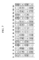
- FIGS. 7 and 8 each illustrate the polarity dispositions of the n-th frame and the n+1-th frame at the time of displaying mixed color.
- the “a”, “b”, “c”, and “d” are respectively red, green, blue, and white, and the display panel displays cyan.
- the polarities of the subpixels each representing the green “b” and the blue “c” are inverted in the n-th frame and the n+1-th frame, the number of positive (+) subpixels and negative ( ⁇ ) subpixels are alternately disposed in each frame. Therefore, even in the case of displaying mixed color, a difference in luminance does not occur between the frames.
- FIGS. 9 to 11 are diagrams illustrating an example of a data voltage applied to a data line in the liquid crystal display according to a first exemplary embodiment of the present invention.
- FIG. 9 illustrates the data voltage applied to the data line when the same data voltage, for example, the maximum gray voltage, is applied to all the subpixels.
- one unit in the horizontal direction indicates one horizontal period “1H”.
- the voltage applied to the first data line D 1 and the voltage applied to the second data line D 2 have the same magnitude but opposite polarities.
- the pair of third and fourth data lines D 3 and D 4 , the pair of fifth and sixth data lines D 5 and D 6 , and the pair of seventh and eighth data lines D 7 and D 8 also have the same relationship. Therefore, because the data voltage is applied to the data line in a complementary manner (i.e., having the same magnitude but an opposed polarity), the polarities of the data voltage are balanced. As the result, the polarity of the data voltage is not biased to any one side and therefore, the data voltage does not affect the common voltage Vcom.
- FIG. 10 illustrates the data voltage applied to the data line when the monochrome is displayed by applying the maximum gray voltage only to the subpixel of the color “b” (e.g., green) and the minimum gray voltage to the subpixels of the remaining colors.
- the data voltages applied to the first and third data lines D 1 and D 3 and the data voltages applied to the fifth and seventh data lines D 5 and D 7 have the same magnitude and an opposed polarity.
- the voltage applied to the second data line D 2 and the voltage applied to the sixth data line D 6 have the same magnitude but opposite polarities, and when any one of the voltages rises, the other thereof falls.
- the voltage applied to the fourth data line D 4 and the voltage applied to the eighth data line D 8 are the same magnitude and an opposed polarity and when nay one of the voltages rises, the other of thereof falls. Therefore, because the voltage is complementarily applied to the data line and is also applied to prevent the rising and falling of the voltage, the polarity of the data voltage is not biased to any one side at the time of displaying the monochrome, and therefore the data voltage does not affect the common voltage Vcom.
- FIG. 11 illustrates the data voltage applied to the data line when the mixed color (e.g., cyan) is displayed by applying the maximum gray voltage to the subpixel of the color “b” (e.g., green) and the subpixel of the color “c” (e.g., blue), and applying the minimum gray voltage to the subpixels of the remaining colors.
- a voltage is applied in a complementary manner to the first data line D 1 and the fifth data line D 5 . This relationship is also shown between the second and sixth data lines D 2 and D 6 , between the third and seventh data lines D 3 and D 7 , and between the fourth and eighth data lines D 4 and D 8 .
- the voltage is applied in a complementary manner to the data line and is also applied to prevent the rising and falling of the voltage, the data voltage is not biased to any one side, and therefore the data voltage does not affect the common voltage Vcom even at the time of displaying the mixed color.
- FIGS. 12 to 17 are diagrams illustrating a polarity disposition and an inversion driving of the liquid crystal display according to a second exemplary embodiment of the present invention.
- FIGS. 12 and 13 each illustrate the polarity dispositions in the n-th frame and the n+1-th frame, respectively, in the liquid crystal display.
- each of the data lines is connected to the subpixels, which are located at the right thereof. Therefore, a difference in luminance due to the characteristic deviation such as the Cgs of the thin film transistor between the subpixels does not occur.
- Each of the data lines all may be connected to the subpixels which are located at the left thereof, as shown in FIG. 12 , but the present invention is not so limited, and any data line may be connected to the subpixels which are located only at the right thereof, and any data line may be connected to the subpixels which are located only to the left thereof.
- the positive (+) data voltage and the negative ( ⁇ ) data voltage are repeatedly applied to the first, third, sixth, and eighth data lines D 1 , D 3 , D 6 , and D 8 for each three subpixels in the column direction, and the negative ( ⁇ ) data voltage and the positive (+) data voltage are repeatedly applied to the second, fourth, fifth and seventh data lines D 2 , D 4 , D 5 , and D 7 for each three subpixels in the column direction. That is, in contrast to the first exemplary embodiment, in the second exemplary embodiment, the data voltage having the same polarity is not applied to the corresponding data line over one frame, but the data voltage having the polarity inverted for each three subpixels in each column is applied thereto.
- the positive (+) data voltage is applied to the subpixels which are connected to the first to third gate lines of the corresponding data line
- the negative ( ⁇ ) data voltage is applied to the subpixels which are connected to the fourth to sixth gate lines
- the inversion driving is repeated for the corresponding data line.
- the data voltage is applied inversely to the n-th frame. That is, the negative ( ⁇ ) data voltage and the positive (+) data voltage are repeatedly applied to the first, third, sixth, and eighth data lines D 1 , D 3 , D 6 , and D 8 for each three subpixels in the column direction. Similarly, the positive (+) data voltage and the negative ( ⁇ ) data voltage are repeatedly applied to the second, fourth, fifth, and seventh data lines D 2 , D 4 , D 5 , and D 7 for each three subpixels in the column direction.
- the application of the data voltage having different polarities depending on the data line, and for every group of three gate lines, is repeated based on eight data lines. Therefore, the polarity of the data voltage applied to the first to eighth data lines D 1 to D 8 may also be similarly applied to the ninth to sixteenth data lines D 9 to D 16 .
- the data driver 500 may apply the data voltage having a polarity inverted for each frame, and the data voltage having a polarity inverted for each three gate lines in one frame to each data line so as to meet the foregoing polarity.
- the subpixels located in the first to fourth columns have the inverted polarity between the adjacent subpixels, and the subpixels that are located in the fifth to eighth columns also have the inverted polarity between the adjacent subpixels, but polarities of the subpixels that are located in the fifth to eighth columns are opposite to those of the subpixels that are located in the first to fourth columns, respectively. Further, the subpixels that are located in the first to eighth columns have a polarity inverted for each three subpixels in each column.
- the first to eighth subpixel arrays configure a basic unit and are repeated in the row direction. That is, the polarities of the ninth to sixteenth subpixel arrays are sequentially the same as those of the first to eighth subpixel arrays.
- the number of positive (+) subpixels is the same as the number of negative ( ⁇ ) subpixels for each color in the n-th frame and the n+1-th frame (therefore, all frames), and the positive (+) subpixels and the negative ( ⁇ ) subpixels are alternately disposed in the row direction for each color. Therefore, because the positive polarity and the negative polarity are evenly mixed, the deterioration in display quality resulting from a difference in luminance, which may be present between polarities, does not occur, and the difference in luminance between the frames resulting from polarity mismatching does not also occur.
- FIGS. 14 and 15 illustrate the polarity dispositions of the n-th frame and the n+1-th frame at the time of displaying only one color. For example, when “a” is red, even though the polarity of the subpixel representing the red “a” is inverted in the n-th frame and the n+1-th frame, the number of positive (+) subpixels and negative ( ⁇ ) subpixels are alternately disposed in each frame. Therefore, even in the case of displaying the monochrome, the difference in luminance does not occur between the frames.
- FIGS. 16 and 17 each illustrate the polarity dispositions of the n-th frame and the n+1-th frame at the time of displaying mixed color.
- “a”, “b”, “c”, and “d” each are red, green, blue, and white
- the number of positive (+) subpixels and negative ( ⁇ ) subpixels are alternately disposed in each frame. Therefore, even in the case of displaying mixed color, a difference in luminance does not occur between the frames.
- FIGS. 18 to 20 are diagrams illustrating an example of a data voltage applied to a data line in the liquid crystal display according to the second exemplary embodiment of the present invention.
- FIG. 18 illustrates the data voltage applied to the data line when the same data voltage, for example, the maximum gray voltage is applied to all the subpixels.
- one unit in the horizontal direction indicates one horizontal time period “1H”.
- the voltage applied to the first data line D 1 and the voltage applied to the second data line D 2 have the same magnitude but an opposed polarity, and when one of the voltages rises the other thereof falls. Therefore, the voltages applied to the first and second data lines D 1 and D 2 are complementary.
- the data voltages which are each applied to the third and fourth data lines D 3 and D 4 , the fifth and sixth data lines D 5 and D 6 , and the seventh and eighth data lines D 7 and D 8 are also complementary. Therefore, the data voltage is not biased to any one side and, therefore, does not affect the common voltage Vcom.
- FIG. 19 illustrates the data voltage applied to the data line when the monochrome is displayed by applying the maximum gray voltage only to the subpixel of the color “a” (e.g., red) and the minimum gray voltage to the subpixels of the remaining colors.
- the data voltage is complementarily applied to each pair of the first and fifth data lines D 1 and D 5 , the second and sixth data lines D 2 and D 6 , the third and seventh data lines D 3 and D 7 , and the fourth and eighth data lines D 4 and D 8 . Therefore, when the monochrome is displayed, the data voltage is not biased to any one side, but is instead balanced.
- FIG. 20 illustrates the data voltage applied to the data line when a mixed color (e.g., cyan) is displayed by applying the maximum gray voltage to the subpixel of the color “b” (e.g., green) and the subpixel of the color “c” (e.g., blue) and applying the minimum gray voltage to the subpixels of the remaining colors.
- the data voltage is complementarily applied to the first and eighth data lines D 1 and D 8 and the fourth and fifth data lines D 4 and D 5 . Further, the data voltage is complementarily applied to the second and seventh data lines D 2 and D 7 and the third and sixth data lines D 3 and D 6 . Therefore, the data voltage is not biased to any one side and, therefore, does not affect the common voltage Vcom even at the time of displaying the mixed color.
- FIGS. 21 to 26 are diagrams illustrating polarity dispositions of liquid crystal displays according to various other exemplary embodiments of the present invention.
- FIG. 21 illustrates the polarity disposition according to a third exemplary embodiment of the present invention.
- the data lines are alternately connected to the subpixels, which are located at the left and right thereof, one-by-one.
- the positive (+) data voltage is applied to the first and second data lines D 1 and D 2
- the negative ( ⁇ ) data voltage is applied to the third and fourth data lines D 3 and D 4 .
- the data voltage is repeatedly applied in the row direction based on four data lines as the basic unit. Therefore, the data voltages having the polarity applied to the first to fourth data lines D 1 to D 4 is also applied to the fifth to eighth data lines D 5 to D 8 , respectively.
- the data lines are alternately connected to the subpixels which are located at the right and left thereof, the positive (+) voltage is applied to all the subpixels of the first column, and the negative ( ⁇ ) voltage is applied to all the subpixels of the third column, but the positive (+) voltage and the negative ( ⁇ ) voltage are alternately applied to the subpixels of the second column, and the negative ( ⁇ ) voltage and the positive (+) voltage are alternately applied to the subpixels of the fourth column.
- the voltage having a polarity different from that of the voltage applied to the current frame is applied to each of the data lines in the next frame, and each subpixel also has the inverted polarity.
- FIG. 22 illustrates the polarity disposition according to a fourth exemplary embodiment of the present invention.
- the data lines are alternately connected to the subpixels, which are located at the left and right thereof, one-by-one.
- the positive (+) data voltage and the negative ( ⁇ ) data voltage are alternately applied to the first, third, sixth, and eighth data lines D 1 , D 3 , D 6 , and D 8 for each three subpixels in the column direction
- the negative ( ⁇ ) data voltage and the positive (+) data voltage are alternately applied to the second, fourth, fifth and seventh data lines D 2 , D 4 , D 5 , and D 7 for each three subpixels in the column direction.
- the data voltage is repeatedly applied in the row direction based on eight data lines as the basic unit, and the polarity of the data voltage applied to each data line is inverted for each frame.
- the subpixels of the first to third columns and the fifth to seventh columns have the inverted polarity between the adjacent subpixels in each repetitive unit based on three subpixels as the repetitive unit, but the subpixels of the fourth and eighth columns have the inverted polarity for each three subpixels.
- FIG. 23 illustrates the polarity disposition according to a fifth exemplary embodiment of the present invention.
- the data lines are alternately connected to the subpixels, which are located at the left and right thereof, one-by-one.
- the positive (+) data voltage and the negative ( ⁇ ) data voltage are alternately applied to the first to fourth data lines D 1 to D 4 for each three subpixels in the column direction
- the negative ( ⁇ ) data voltage and the positive (+) data voltage are alternately applied to the fifth to eighth data lines D 5 to D 8 for each three subpixels in the column direction.
- the data voltage is repeatedly applied in the row direction based on eight data lines as the basic unit, and is inverted for each frame.
- the subpixels of the first to third columns and the fifth to seventh columns have the inverted for each three subpixels, but the subpixels of the fourth and eighth columns have the inverted polarity between the adjacent subpixels in each repetitive unit based on three subpixels as the repetitive unit.
- the number of positive (+) subpixels is the same as the number of negative ( ⁇ ) subpixels for each color, and the positive (+) subpixels and the negative ( ⁇ ) subpixels are alternately disposed in the row direction for each color.
- the voltage may be complementarily applied to the data line. Therefore, the difference in luminance resulting from polarity mismatching, or the ripple of the common voltage resulting from the polarity biasing does not occur.
- FIG. 24 illustrates the polarity disposition according to a sixth exemplary embodiment of the present invention.
- the data lines are alternately connected to the subpixels, which are located at the left and right thereof, two-by-two.
- the positive (+) data voltage is applied to the first and second data lines D 1 and D 2
- the negative ( ⁇ ) data voltage is applied to the third and fourth data lines D 3 and D 4 .
- the data voltage is repeatedly applied in the row direction based on four data lines as the basic unit.
- the data lines are alternately connected to the subpixels, which are located at the right and left thereof, two-by-two, the positive (+) voltage is applied to all the subpixels of the first column and the negative ( ⁇ ) voltage are alternately applied to all the subpixels of the third column, but the positive (+) voltage and the negative ( ⁇ ) voltage are alternately applied to the subpixels of the second column for each two subpixels in the column direction, and the negative ( ⁇ ) voltage and the positive (+) voltage are alternately applied to the subpixels of the fourth column for each two subpixels in the column direction.
- the voltage having a polarity different from that of the voltage applied to the current frame is applied to each of the data lines in the next frame, and each subpixel also has the inverted polarity.
- FIG. 25 illustrates the polarity disposition according to a seventh exemplary embodiment of the present invention.
- the data lines are alternately connected to the subpixels, which are located at the left and right thereof, two-by-two.
- the positive (+) data voltage and the negative ( ⁇ ) data voltage are alternately applied to the first to third data lines D 1 to D 3 for each four subpixels in the column direction
- the negative ( ⁇ ) data voltage and the positive (+) data voltage are alternately applied to the fourth to sixth data lines D 4 to D 6 for each four subpixels in the column direction.
- the data voltage is repeatedly applied in the row direction based on six data lines as the basic unit, and is inverted in each frame.
- the polarities of the subpixels of each column are inverted for each four subpixels, but the polarities of the subpixels of the third column and the sixth column are inverted at a period different from that of the subpixels of other columns.
- FIG. 26 illustrates the polarity disposition according to an eighth exemplary embodiment of the present invention.
- the data lines are alternately connected to the subpixels, which are located at the left and right thereof, two-by-two.
- the positive (+) data voltage is applied to the first to third data lines D 1 to D 3 and the negative ( ⁇ ) data voltage is applied to the fourth to sixth data lines D 4 to D 6 .
- the data voltage is repeatedly applied in the row direction based on six data lines as the basic unit.
- the positive (+) data voltage is alternately applied to the subpixels of the first and second columns
- the negative ( ⁇ ) data voltage is alternately applied to the subpixels of the fourth and fifth columns
- the positive (+) data voltage and the negative ( ⁇ ) data voltage are alternately applied to the subpixels of the third column for each two subpixels
- the negative ( ⁇ ) data voltage and the positive (+) data voltage are alternately applied to the subpixels of the sixth column for each two subpixels.
- the data voltage having different polarities is applied to each subpixel.
- the voltage may be applied to the data lines in a complementary manner. Therefore, the difference in luminance resulting from the polarity mismatching does not substantially occur, and the ripple of the common voltage resulting from polarity biasing does not occur.
- FIGS. 27 and 28 are diagrams illustrating an example of a polarity disposition of the liquid crystal display in which polarity biasing of the data voltage occurs.
- each of the data lines is connected only to the subpixel which is located at the right thereof.
- the positive (+) data voltage is applied to the first and fourth data lines
- the negative ( ⁇ ) data voltage is applied to the second and third data lines.
- the data voltage is repeatedly applied in the row direction based on six data lines as the basic unit, and is inverted for each frame.
- FIG. 28 illustrates that in the subpixel disposition structure of FIG. 27 , in which the minimum gray voltage is applied to the subpixels of the colors “a” and “d” so as to display the mixed color, and the maximum gray voltage is applied to the colors “b” and “c”.
- one unit in the horizontal direction indicates one horizontal time period “1H”.
- the voltage applied to any data line is not complementary, and when the voltage of any one data line rises, the voltage of the remaining data lines also rises, and when the voltage of any one data line falls, the voltage of the remaining data lines also falls.
- polarity biasing of the data voltage occurs and, therefore, a ripple phenomenon in which the common voltage is undesirably moved as a result of polarity biasing may occur. This may lead to the deterioration in image quality.
- a ripple phenomenon of the common voltage or the deterioration in image quality as a result of polarity biasing does not occur.
Landscapes
- Physics & Mathematics (AREA)
- Engineering & Computer Science (AREA)
- General Physics & Mathematics (AREA)
- Crystallography & Structural Chemistry (AREA)
- Chemical & Material Sciences (AREA)
- Theoretical Computer Science (AREA)
- Computer Hardware Design (AREA)
- Nonlinear Science (AREA)
- Mathematical Physics (AREA)
- Optics & Photonics (AREA)
- Microelectronics & Electronic Packaging (AREA)
- Liquid Crystal (AREA)
- Control Of Indicators Other Than Cathode Ray Tubes (AREA)
- Liquid Crystal Display Device Control (AREA)
Applications Claiming Priority (2)
| Application Number | Priority Date | Filing Date | Title |
|---|---|---|---|
| KR10-2013-0155780 | 2013-12-13 | ||
| KR1020130155780A KR102143926B1 (ko) | 2013-12-13 | 2013-12-13 | 액정 표시 장치 및 그 구동 방법 |
Publications (2)
| Publication Number | Publication Date |
|---|---|
| US20150170590A1 US20150170590A1 (en) | 2015-06-18 |
| US9934736B2 true US9934736B2 (en) | 2018-04-03 |
Family
ID=53369209
Family Applications (1)
| Application Number | Title | Priority Date | Filing Date |
|---|---|---|---|
| US14/328,240 Active 2034-10-15 US9934736B2 (en) | 2013-12-13 | 2014-07-10 | Liquid crystal display and method for driving the same |
Country Status (5)
| Country | Link |
|---|---|
| US (1) | US9934736B2 (ja) |
| JP (1) | JP6552181B2 (ja) |
| KR (1) | KR102143926B1 (ja) |
| CN (1) | CN104714318B (ja) |
| TW (1) | TWI637378B (ja) |
Families Citing this family (29)
| Publication number | Priority date | Publication date | Assignee | Title |
|---|---|---|---|---|
| KR20150139132A (ko) | 2014-06-02 | 2015-12-11 | 삼성디스플레이 주식회사 | 표시 장치 및 그 구동 방법 |
| KR102269487B1 (ko) | 2014-06-17 | 2021-06-28 | 삼성디스플레이 주식회사 | 표시 패널의 구동 방법 및 이를 수행하기 위한 표시 장치 |
| US10147371B2 (en) * | 2014-06-27 | 2018-12-04 | Lg Display Co., Ltd. | Display device having pixels with shared data lines |
| KR102340289B1 (ko) | 2014-08-20 | 2021-12-17 | 삼성디스플레이 주식회사 | 표시 패널의 구동 방법 및 이를 수행하기 위한 표시 장치 |
| KR20160029892A (ko) | 2014-09-05 | 2016-03-16 | 삼성디스플레이 주식회사 | 표시 장치 및 그것의 구동 방법 |
| KR20160072369A (ko) | 2014-12-12 | 2016-06-23 | 삼성디스플레이 주식회사 | 표시장치 |
| KR102342685B1 (ko) | 2015-03-05 | 2021-12-24 | 삼성디스플레이 주식회사 | 표시 패널 및 이를 포함하는 표시 장치 |
| US9786235B2 (en) * | 2015-06-15 | 2017-10-10 | Shenzhen China Star Optoelectronics Technology Co., Ltd. | Pixel structure having opposite sub-pixel polarities in adjacent pixel columns and liquid crystal display panel having same |
| CN105096802A (zh) * | 2015-08-21 | 2015-11-25 | 深圳市华星光电技术有限公司 | 一种四色显示器的驱动方法及装置 |
| CN105319786B (zh) * | 2015-11-26 | 2018-06-19 | 深圳市华星光电技术有限公司 | 具有低切换频率的数据线驱动极性的阵列基板 |
| CN105404034B (zh) * | 2015-12-03 | 2019-02-01 | 深圳市华星光电技术有限公司 | 液晶面板、液晶显示装置及像素阵列 |
| CN105702226B (zh) * | 2016-04-28 | 2018-07-17 | 京东方科技集团股份有限公司 | 一种显示面板的驱动方法、显示面板及显示装置 |
| US10061167B2 (en) * | 2016-05-29 | 2018-08-28 | Novatek Microelectronics Corp. | Display device with novel sub-pixel arrangement |
| CN106023938A (zh) * | 2016-07-29 | 2016-10-12 | 深圳市华星光电技术有限公司 | 液晶显示器及其驱动方法 |
| TWI622039B (zh) * | 2017-01-05 | 2018-04-21 | 友達光電股份有限公司 | 顯示裝置 |
| CN106920500B (zh) * | 2017-05-02 | 2020-09-11 | 惠科股份有限公司 | 显示驱动方法及显示驱动装置 |
| US20200160803A1 (en) * | 2017-05-30 | 2020-05-21 | Sharp Kabushiki Kaisha | Liquid crystal display device |
| US10690980B2 (en) * | 2017-12-18 | 2020-06-23 | Shenzhen China Star Optoelectronics Semiconductor Display Technology Co., Ltd. | Array substrate and driving method thereof and liquid crystal panel |
| CN108109599B (zh) * | 2017-12-19 | 2019-12-10 | 惠科股份有限公司 | 一种显示面板、显示装置及驱动方法 |
| CN107978288B (zh) * | 2017-12-19 | 2020-04-07 | 惠科股份有限公司 | 一种显示面板、显示装置及驱动方法 |
| CN108181770A (zh) * | 2018-02-11 | 2018-06-19 | 厦门天马微电子有限公司 | 一种显示面板及显示装置 |
| CN108198539A (zh) * | 2018-02-13 | 2018-06-22 | 厦门天马微电子有限公司 | 显示面板及其驱动方法、显示装置 |
| CN110570801B (zh) * | 2018-12-05 | 2022-12-06 | 友达光电股份有限公司 | 显示装置 |
| CN111489712B (zh) * | 2019-01-29 | 2022-03-11 | 咸阳彩虹光电科技有限公司 | 一种像素矩阵驱动装置及显示器 |
| CN111489713B (zh) * | 2019-01-29 | 2023-02-03 | 咸阳彩虹光电科技有限公司 | 一种像素矩阵驱动装置及显示器 |
| CN110233807B (zh) * | 2019-05-08 | 2022-07-15 | 合肥杰发科技有限公司 | 一种低压差分信号发送器以及数据传输设备 |
| CN110459187B (zh) * | 2019-08-15 | 2021-08-06 | 京东方科技集团股份有限公司 | 透明显示器的驱动方法、驱动装置及显示装置 |
| CN111061106B (zh) * | 2020-01-02 | 2022-09-09 | 福州京东方光电科技有限公司 | 一种阵列基板及显示面板 |
| US11721298B2 (en) * | 2021-12-24 | 2023-08-08 | Tcl China Star Optoelectronics Technology Co., Ltd. | Display panel and display device |
Citations (19)
| Publication number | Priority date | Publication date | Assignee | Title |
|---|---|---|---|---|
| US6552707B1 (en) | 1998-05-11 | 2003-04-22 | Alps Electric Co., Ltd. | Drive method for liquid crystal display device and drive circuit |
| US20060202927A1 (en) * | 2003-04-17 | 2006-09-14 | Lee Baek-Woon | Liquid crystal display |
| US20060208984A1 (en) * | 2004-11-12 | 2006-09-21 | Kim Sang-Soo | Display device and driving method thereof |
| US20070069214A1 (en) | 2005-09-29 | 2007-03-29 | Samsung Electronics Co., Ltd. | Liquid crystal display and method of driving the same |
| CN1998041A (zh) | 2002-01-07 | 2007-07-11 | 美商克莱佛扬实验室公司 | 具有分裂蓝色子像素的子像素着色的彩色平板显示器 |
| KR20080001052A (ko) | 2006-06-29 | 2008-01-03 | 엘지.필립스 엘시디 주식회사 | 액정표시장치 및 그의 구동방법 |
| US20080158131A1 (en) | 2006-11-24 | 2008-07-03 | Keun-Woo Park | LCD data drivers |
| CN101317212A (zh) | 2005-11-30 | 2008-12-03 | 夏普株式会社 | 用于驱动显示元件的显示设备和方法 |
| US20100002021A1 (en) | 2008-06-30 | 2010-01-07 | Nec Electronics Corporation | Display panel driving method and display apparatus |
| US20100073617A1 (en) | 2008-09-25 | 2010-03-25 | Seung Woo Han | Array substrate, liquid crystal panel and liquid crystal display device |
| US7724224B2 (en) | 2004-02-25 | 2010-05-25 | Samsung Electronics Co., Ltd. | Display device |
| US20110012887A1 (en) | 2009-07-15 | 2011-01-20 | Samsung Electronics Co., Ltd | Display apparatus |
| US20110134103A1 (en) | 2009-12-03 | 2011-06-09 | Nam Yousung | Liquid crystal display |
| KR20110077899A (ko) | 2009-12-30 | 2011-07-07 | 삼성전자주식회사 | 표시 장치 |
| JP2011209453A (ja) | 2010-03-29 | 2011-10-20 | Renesas Electronics Corp | 液晶表示装置、液晶表示装置の駆動方法 |
| US8264656B2 (en) | 2008-12-02 | 2012-09-11 | Samsung Electronics Co., Ltd. | Liquid crystal display and manufacturing method thereof |
| CN103185996A (zh) | 2011-12-30 | 2013-07-03 | 上海中航光电子有限公司 | 横向排列的rgbw像素结构及其驱动方法、显示面板 |
| US20140232624A1 (en) | 2013-02-18 | 2014-08-21 | Samsung Display Co., Ltd. | Display device |
| US9183799B2 (en) * | 2011-05-24 | 2015-11-10 | Apple Inc. | Additional application of voltage during a write sequence |
Family Cites Families (5)
| Publication number | Priority date | Publication date | Assignee | Title |
|---|---|---|---|---|
| KR20060082104A (ko) * | 2005-01-11 | 2006-07-14 | 삼성전자주식회사 | 액정 표시 장치 및 그 구동 방법 |
| KR101179233B1 (ko) * | 2005-09-12 | 2012-09-04 | 삼성전자주식회사 | 액정표시장치 및 그 제조방법 |
| KR101323090B1 (ko) * | 2009-03-11 | 2013-10-29 | 엘지디스플레이 주식회사 | 액정표시장치와 그 구동방법 |
| JP5301681B2 (ja) * | 2009-11-20 | 2013-09-25 | シャープ株式会社 | 液晶表示装置 |
| KR101201417B1 (ko) * | 2011-10-28 | 2012-11-14 | 삼성디스플레이 주식회사 | 액정표시장치 및 그 제조방법 |
-
2013
- 2013-12-13 KR KR1020130155780A patent/KR102143926B1/ko active Active
-
2014
- 2014-07-10 US US14/328,240 patent/US9934736B2/en active Active
- 2014-09-22 TW TW103132611A patent/TWI637378B/zh active
- 2014-10-23 CN CN201410571819.3A patent/CN104714318B/zh active Active
- 2014-11-06 JP JP2014226372A patent/JP6552181B2/ja active Active
Patent Citations (21)
| Publication number | Priority date | Publication date | Assignee | Title |
|---|---|---|---|---|
| US6552707B1 (en) | 1998-05-11 | 2003-04-22 | Alps Electric Co., Ltd. | Drive method for liquid crystal display device and drive circuit |
| CN1998041A (zh) | 2002-01-07 | 2007-07-11 | 美商克莱佛扬实验室公司 | 具有分裂蓝色子像素的子像素着色的彩色平板显示器 |
| US20060202927A1 (en) * | 2003-04-17 | 2006-09-14 | Lee Baek-Woon | Liquid crystal display |
| US7724224B2 (en) | 2004-02-25 | 2010-05-25 | Samsung Electronics Co., Ltd. | Display device |
| US20060208984A1 (en) * | 2004-11-12 | 2006-09-21 | Kim Sang-Soo | Display device and driving method thereof |
| US20070069214A1 (en) | 2005-09-29 | 2007-03-29 | Samsung Electronics Co., Ltd. | Liquid crystal display and method of driving the same |
| CN101317212A (zh) | 2005-11-30 | 2008-12-03 | 夏普株式会社 | 用于驱动显示元件的显示设备和方法 |
| US20090040243A1 (en) | 2005-11-30 | 2009-02-12 | Yuhko Hisada | Display Device and Method for Driving Display Member |
| KR20080001052A (ko) | 2006-06-29 | 2008-01-03 | 엘지.필립스 엘시디 주식회사 | 액정표시장치 및 그의 구동방법 |
| US20080158131A1 (en) | 2006-11-24 | 2008-07-03 | Keun-Woo Park | LCD data drivers |
| US20100002021A1 (en) | 2008-06-30 | 2010-01-07 | Nec Electronics Corporation | Display panel driving method and display apparatus |
| US20100073617A1 (en) | 2008-09-25 | 2010-03-25 | Seung Woo Han | Array substrate, liquid crystal panel and liquid crystal display device |
| US8264656B2 (en) | 2008-12-02 | 2012-09-11 | Samsung Electronics Co., Ltd. | Liquid crystal display and manufacturing method thereof |
| US20110012887A1 (en) | 2009-07-15 | 2011-01-20 | Samsung Electronics Co., Ltd | Display apparatus |
| US20110134103A1 (en) | 2009-12-03 | 2011-06-09 | Nam Yousung | Liquid crystal display |
| KR20110077899A (ko) | 2009-12-30 | 2011-07-07 | 삼성전자주식회사 | 표시 장치 |
| JP2011209453A (ja) | 2010-03-29 | 2011-10-20 | Renesas Electronics Corp | 液晶表示装置、液晶表示装置の駆動方法 |
| US9183799B2 (en) * | 2011-05-24 | 2015-11-10 | Apple Inc. | Additional application of voltage during a write sequence |
| CN103185996A (zh) | 2011-12-30 | 2013-07-03 | 上海中航光电子有限公司 | 横向排列的rgbw像素结构及其驱动方法、显示面板 |
| US20140232624A1 (en) | 2013-02-18 | 2014-08-21 | Samsung Display Co., Ltd. | Display device |
| KR20140103588A (ko) | 2013-02-18 | 2014-08-27 | 삼성디스플레이 주식회사 | 표시 장치 |
Also Published As
| Publication number | Publication date |
|---|---|
| TWI637378B (zh) | 2018-10-01 |
| KR102143926B1 (ko) | 2020-08-13 |
| KR20150069411A (ko) | 2015-06-23 |
| CN104714318A (zh) | 2015-06-17 |
| JP2015114663A (ja) | 2015-06-22 |
| JP6552181B2 (ja) | 2019-07-31 |
| CN104714318B (zh) | 2020-03-10 |
| US20150170590A1 (en) | 2015-06-18 |
| TW201523568A (zh) | 2015-06-16 |
Similar Documents
| Publication | Publication Date | Title |
|---|---|---|
| US9934736B2 (en) | Liquid crystal display and method for driving the same | |
| CN106067293B (zh) | 液晶显示器 | |
| US9870749B2 (en) | Display device | |
| US9613577B2 (en) | Display device and method of driving the same | |
| US9570020B2 (en) | Display device having subpixels of four colors in each pixel | |
| US11475857B2 (en) | Array substrate and display device | |
| US20110249046A1 (en) | Liquid crystal display device | |
| US11527213B2 (en) | Driving method of display panel for reducing viewing angle color deviation and display device | |
| CN105047167B (zh) | 一种源极驱动电路、显示装置及其驱动方法 | |
| CN105652540A (zh) | 显示面板 | |
| WO2017015972A1 (zh) | 一种液晶显示器 | |
| US20170103723A1 (en) | Display device and driving method thereof | |
| US20170032749A1 (en) | Liquid crystal display device | |
| US20160232862A1 (en) | Display apparatus | |
| KR102169032B1 (ko) | 표시장치 | |
| KR20130051773A (ko) | 액정표시장치의 인버전 구동방법 | |
| KR20030058140A (ko) | 액정표시장치의 구동방법 | |
| KR102244985B1 (ko) | 표시패널 | |
| KR101686093B1 (ko) | 시야각 제어 액정 표시 장치 및 이의 구동 방법 | |
| KR102160121B1 (ko) | 표시장치 | |
| KR20160029225A (ko) | 액정표시장치 | |
| KR102437757B1 (ko) | 액정 표시패널 및 액정 표시장치 | |
| KR102169963B1 (ko) | 액정표시장치 및 이의 도트 인버전 제어방법 | |
| KR102352594B1 (ko) | 표시장치 |
Legal Events
| Date | Code | Title | Description |
|---|---|---|---|
| AS | Assignment |
Owner name: SAMSUNG DISPLAY CO., LTD., KOREA, REPUBLIC OF Free format text: ASSIGNMENT OF ASSIGNORS INTEREST;ASSIGNORS:AHN, KUK-HWAN;KOH, JAI-HYUN;KIM, JIN PIL;AND OTHERS;REEL/FRAME:033289/0426 Effective date: 20140411 |
|
| STCF | Information on status: patent grant |
Free format text: PATENTED CASE |
|
| MAFP | Maintenance fee payment |
Free format text: PAYMENT OF MAINTENANCE FEE, 4TH YEAR, LARGE ENTITY (ORIGINAL EVENT CODE: M1551); ENTITY STATUS OF PATENT OWNER: LARGE ENTITY Year of fee payment: 4 |
|
| MAFP | Maintenance fee payment |
Free format text: PAYMENT OF MAINTENANCE FEE, 8TH YEAR, LARGE ENTITY (ORIGINAL EVENT CODE: M1552); ENTITY STATUS OF PATENT OWNER: LARGE ENTITY Year of fee payment: 8 |