US9847362B2 - Semiconductor photosensitive unit and semiconductor photosensitive unit array thereof - Google Patents
Semiconductor photosensitive unit and semiconductor photosensitive unit array thereof Download PDFInfo
- Publication number
- US9847362B2 US9847362B2 US15/126,580 US201515126580A US9847362B2 US 9847362 B2 US9847362 B2 US 9847362B2 US 201515126580 A US201515126580 A US 201515126580A US 9847362 B2 US9847362 B2 US 9847362B2
- Authority
- US
- United States
- Prior art keywords
- conductivity type
- floating gate
- semiconductor
- semiconductor photosensitive
- photosensitive unit
- Prior art date
- Legal status (The legal status is an assumption and is not a legal conclusion. Google has not performed a legal analysis and makes no representation as to the accuracy of the status listed.)
- Active
Links
- 239000004065 semiconductor Substances 0.000 title claims abstract description 198
- 238000007667 floating Methods 0.000 claims abstract description 129
- 239000000758 substrate Substances 0.000 claims abstract description 55
- 238000009413 insulation Methods 0.000 claims description 29
- 238000009792 diffusion process Methods 0.000 claims description 23
- 230000001808 coupling effect Effects 0.000 claims description 5
- 238000010586 diagram Methods 0.000 description 20
- 239000000463 material Substances 0.000 description 16
- XUIMIQQOPSSXEZ-UHFFFAOYSA-N Silicon Chemical compound [Si] XUIMIQQOPSSXEZ-UHFFFAOYSA-N 0.000 description 10
- 229910052751 metal Inorganic materials 0.000 description 10
- 239000002184 metal Substances 0.000 description 10
- 229910052710 silicon Inorganic materials 0.000 description 10
- 239000010703 silicon Substances 0.000 description 10
- 229910000577 Silicon-germanium Inorganic materials 0.000 description 7
- LEVVHYCKPQWKOP-UHFFFAOYSA-N [Si].[Ge] Chemical compound [Si].[Ge] LEVVHYCKPQWKOP-UHFFFAOYSA-N 0.000 description 7
- 238000004519 manufacturing process Methods 0.000 description 7
- VYPSYNLAJGMNEJ-UHFFFAOYSA-N Silicium dioxide Chemical compound O=[Si]=O VYPSYNLAJGMNEJ-UHFFFAOYSA-N 0.000 description 6
- 229910052732 germanium Inorganic materials 0.000 description 6
- GNPVGFCGXDBREM-UHFFFAOYSA-N germanium atom Chemical compound [Ge] GNPVGFCGXDBREM-UHFFFAOYSA-N 0.000 description 6
- RTAQQCXQSZGOHL-UHFFFAOYSA-N Titanium Chemical compound [Ti] RTAQQCXQSZGOHL-UHFFFAOYSA-N 0.000 description 5
- 239000010936 titanium Substances 0.000 description 5
- 229910052719 titanium Inorganic materials 0.000 description 5
- WFKWXMTUELFFGS-UHFFFAOYSA-N tungsten Chemical compound [W] WFKWXMTUELFFGS-UHFFFAOYSA-N 0.000 description 5
- 229910052721 tungsten Inorganic materials 0.000 description 5
- 239000010937 tungsten Substances 0.000 description 5
- 230000008878 coupling Effects 0.000 description 4
- 238000010168 coupling process Methods 0.000 description 4
- 238000005859 coupling reaction Methods 0.000 description 4
- 230000007547 defect Effects 0.000 description 4
- 239000011810 insulating material Substances 0.000 description 4
- 239000007769 metal material Substances 0.000 description 4
- RYGMFSIKBFXOCR-UHFFFAOYSA-N Copper Chemical compound [Cu] RYGMFSIKBFXOCR-UHFFFAOYSA-N 0.000 description 3
- ZOKXTWBITQBERF-UHFFFAOYSA-N Molybdenum Chemical compound [Mo] ZOKXTWBITQBERF-UHFFFAOYSA-N 0.000 description 3
- 229910052581 Si3N4 Inorganic materials 0.000 description 3
- 229910052782 aluminium Inorganic materials 0.000 description 3
- XAGFODPZIPBFFR-UHFFFAOYSA-N aluminium Chemical compound [Al] XAGFODPZIPBFFR-UHFFFAOYSA-N 0.000 description 3
- 229910052802 copper Inorganic materials 0.000 description 3
- 239000010949 copper Substances 0.000 description 3
- PCHJSUWPFVWCPO-UHFFFAOYSA-N gold Chemical compound [Au] PCHJSUWPFVWCPO-UHFFFAOYSA-N 0.000 description 3
- 239000010931 gold Substances 0.000 description 3
- 229910052737 gold Inorganic materials 0.000 description 3
- 230000006872 improvement Effects 0.000 description 3
- 239000000203 mixture Substances 0.000 description 3
- 229910052750 molybdenum Inorganic materials 0.000 description 3
- 239000011733 molybdenum Substances 0.000 description 3
- 150000004767 nitrides Chemical class 0.000 description 3
- 230000002093 peripheral effect Effects 0.000 description 3
- 230000002035 prolonged effect Effects 0.000 description 3
- 229910021332 silicide Inorganic materials 0.000 description 3
- 235000012239 silicon dioxide Nutrition 0.000 description 3
- 239000000377 silicon dioxide Substances 0.000 description 3
- HQVNEWCFYHHQES-UHFFFAOYSA-N silicon nitride Chemical compound N12[Si]34N5[Si]62N3[Si]51N64 HQVNEWCFYHHQES-UHFFFAOYSA-N 0.000 description 3
- NRTOMJZYCJJWKI-UHFFFAOYSA-N Titanium nitride Chemical compound [Ti]#N NRTOMJZYCJJWKI-UHFFFAOYSA-N 0.000 description 2
- 238000013461 design Methods 0.000 description 2
- 230000000694 effects Effects 0.000 description 2
- 238000005516 engineering process Methods 0.000 description 2
- 229910000449 hafnium oxide Inorganic materials 0.000 description 2
- WIHZLLGSGQNAGK-UHFFFAOYSA-N hafnium(4+);oxygen(2-) Chemical compound [O-2].[O-2].[Hf+4] WIHZLLGSGQNAGK-UHFFFAOYSA-N 0.000 description 2
- 230000010354 integration Effects 0.000 description 2
- 230000031700 light absorption Effects 0.000 description 2
- 238000000034 method Methods 0.000 description 2
- TWNQGVIAIRXVLR-UHFFFAOYSA-N oxo(oxoalumanyloxy)alumane Chemical compound O=[Al]O[Al]=O TWNQGVIAIRXVLR-UHFFFAOYSA-N 0.000 description 2
- RVTZCBVAJQQJTK-UHFFFAOYSA-N oxygen(2-);zirconium(4+) Chemical compound [O-2].[O-2].[Zr+4] RVTZCBVAJQQJTK-UHFFFAOYSA-N 0.000 description 2
- 230000008569 process Effects 0.000 description 2
- 229910001928 zirconium oxide Inorganic materials 0.000 description 2
- JBRZTFJDHDCESZ-UHFFFAOYSA-N AsGa Chemical compound [As]#[Ga] JBRZTFJDHDCESZ-UHFFFAOYSA-N 0.000 description 1
- 229910002601 GaN Inorganic materials 0.000 description 1
- 229910001218 Gallium arsenide Inorganic materials 0.000 description 1
- JMASRVWKEDWRBT-UHFFFAOYSA-N Gallium nitride Chemical compound [Ga]#N JMASRVWKEDWRBT-UHFFFAOYSA-N 0.000 description 1
- 238000005452 bending Methods 0.000 description 1
- 239000000969 carrier Substances 0.000 description 1
- 230000008859 change Effects 0.000 description 1
- 238000007599 discharging Methods 0.000 description 1
- 238000005530 etching Methods 0.000 description 1
- 239000012212 insulator Substances 0.000 description 1
- 238000012986 modification Methods 0.000 description 1
- 230000004048 modification Effects 0.000 description 1
- 230000003071 parasitic effect Effects 0.000 description 1
- 238000011160 research Methods 0.000 description 1
- 238000005070 sampling Methods 0.000 description 1
- FVBUAEGBCNSCDD-UHFFFAOYSA-N silicide(4-) Chemical compound [Si-4] FVBUAEGBCNSCDD-UHFFFAOYSA-N 0.000 description 1
- 238000012360 testing method Methods 0.000 description 1
Images


Classifications
-
- H—ELECTRICITY
- H01—ELECTRIC ELEMENTS
- H01L—SEMICONDUCTOR DEVICES NOT COVERED BY CLASS H10
- H01L27/00—Devices consisting of a plurality of semiconductor or other solid-state components formed in or on a common substrate
- H01L27/14—Devices consisting of a plurality of semiconductor or other solid-state components formed in or on a common substrate including semiconductor components sensitive to infrared radiation, light, electromagnetic radiation of shorter wavelength or corpuscular radiation and specially adapted either for the conversion of the energy of such radiation into electrical energy or for the control of electrical energy by such radiation
- H01L27/144—Devices controlled by radiation
- H01L27/146—Imager structures
- H01L27/14601—Structural or functional details thereof
- H01L27/14609—Pixel-elements with integrated switching, control, storage or amplification elements
- H01L27/14612—Pixel-elements with integrated switching, control, storage or amplification elements involving a transistor
- H01L27/14614—Pixel-elements with integrated switching, control, storage or amplification elements involving a transistor having a special gate structure
-
- H—ELECTRICITY
- H01—ELECTRIC ELEMENTS
- H01L—SEMICONDUCTOR DEVICES NOT COVERED BY CLASS H10
- H01L27/00—Devices consisting of a plurality of semiconductor or other solid-state components formed in or on a common substrate
- H01L27/14—Devices consisting of a plurality of semiconductor or other solid-state components formed in or on a common substrate including semiconductor components sensitive to infrared radiation, light, electromagnetic radiation of shorter wavelength or corpuscular radiation and specially adapted either for the conversion of the energy of such radiation into electrical energy or for the control of electrical energy by such radiation
- H01L27/144—Devices controlled by radiation
- H01L27/146—Imager structures
- H01L27/14601—Structural or functional details thereof
- H01L27/14603—Special geometry or disposition of pixel-elements, address-lines or gate-electrodes
-
- H—ELECTRICITY
- H01—ELECTRIC ELEMENTS
- H01L—SEMICONDUCTOR DEVICES NOT COVERED BY CLASS H10
- H01L27/00—Devices consisting of a plurality of semiconductor or other solid-state components formed in or on a common substrate
- H01L27/14—Devices consisting of a plurality of semiconductor or other solid-state components formed in or on a common substrate including semiconductor components sensitive to infrared radiation, light, electromagnetic radiation of shorter wavelength or corpuscular radiation and specially adapted either for the conversion of the energy of such radiation into electrical energy or for the control of electrical energy by such radiation
- H01L27/144—Devices controlled by radiation
- H01L27/146—Imager structures
- H01L27/14601—Structural or functional details thereof
- H01L27/14609—Pixel-elements with integrated switching, control, storage or amplification elements
- H01L27/14612—Pixel-elements with integrated switching, control, storage or amplification elements involving a transistor
- H01L27/14616—Pixel-elements with integrated switching, control, storage or amplification elements involving a transistor characterised by the channel of the transistor, e.g. channel having a doping gradient
-
- H—ELECTRICITY
- H01—ELECTRIC ELEMENTS
- H01L—SEMICONDUCTOR DEVICES NOT COVERED BY CLASS H10
- H01L27/00—Devices consisting of a plurality of semiconductor or other solid-state components formed in or on a common substrate
- H01L27/14—Devices consisting of a plurality of semiconductor or other solid-state components formed in or on a common substrate including semiconductor components sensitive to infrared radiation, light, electromagnetic radiation of shorter wavelength or corpuscular radiation and specially adapted either for the conversion of the energy of such radiation into electrical energy or for the control of electrical energy by such radiation
- H01L27/144—Devices controlled by radiation
- H01L27/146—Imager structures
- H01L27/14601—Structural or functional details thereof
- H01L27/14636—Interconnect structures
-
- H—ELECTRICITY
- H01—ELECTRIC ELEMENTS
- H01L—SEMICONDUCTOR DEVICES NOT COVERED BY CLASS H10
- H01L27/00—Devices consisting of a plurality of semiconductor or other solid-state components formed in or on a common substrate
- H01L27/14—Devices consisting of a plurality of semiconductor or other solid-state components formed in or on a common substrate including semiconductor components sensitive to infrared radiation, light, electromagnetic radiation of shorter wavelength or corpuscular radiation and specially adapted either for the conversion of the energy of such radiation into electrical energy or for the control of electrical energy by such radiation
- H01L27/144—Devices controlled by radiation
- H01L27/146—Imager structures
- H01L27/14643—Photodiode arrays; MOS imagers
-
- H—ELECTRICITY
- H01—ELECTRIC ELEMENTS
- H01L—SEMICONDUCTOR DEVICES NOT COVERED BY CLASS H10
- H01L31/00—Semiconductor devices sensitive to infrared radiation, light, electromagnetic radiation of shorter wavelength or corpuscular radiation and specially adapted either for the conversion of the energy of such radiation into electrical energy or for the control of electrical energy by such radiation; Processes or apparatus specially adapted for the manufacture or treatment thereof or of parts thereof; Details thereof
- H01L31/08—Semiconductor devices sensitive to infrared radiation, light, electromagnetic radiation of shorter wavelength or corpuscular radiation and specially adapted either for the conversion of the energy of such radiation into electrical energy or for the control of electrical energy by such radiation; Processes or apparatus specially adapted for the manufacture or treatment thereof or of parts thereof; Details thereof in which radiation controls flow of current through the device, e.g. photoresistors
- H01L31/10—Semiconductor devices sensitive to infrared radiation, light, electromagnetic radiation of shorter wavelength or corpuscular radiation and specially adapted either for the conversion of the energy of such radiation into electrical energy or for the control of electrical energy by such radiation; Processes or apparatus specially adapted for the manufacture or treatment thereof or of parts thereof; Details thereof in which radiation controls flow of current through the device, e.g. photoresistors characterised by potential barriers, e.g. phototransistors
- H01L31/101—Devices sensitive to infrared, visible or ultraviolet radiation
- H01L31/102—Devices sensitive to infrared, visible or ultraviolet radiation characterised by only one potential barrier
- H01L31/103—Devices sensitive to infrared, visible or ultraviolet radiation characterised by only one potential barrier the potential barrier being of the PN homojunction type
-
- H—ELECTRICITY
- H01—ELECTRIC ELEMENTS
- H01L—SEMICONDUCTOR DEVICES NOT COVERED BY CLASS H10
- H01L31/00—Semiconductor devices sensitive to infrared radiation, light, electromagnetic radiation of shorter wavelength or corpuscular radiation and specially adapted either for the conversion of the energy of such radiation into electrical energy or for the control of electrical energy by such radiation; Processes or apparatus specially adapted for the manufacture or treatment thereof or of parts thereof; Details thereof
- H01L31/08—Semiconductor devices sensitive to infrared radiation, light, electromagnetic radiation of shorter wavelength or corpuscular radiation and specially adapted either for the conversion of the energy of such radiation into electrical energy or for the control of electrical energy by such radiation; Processes or apparatus specially adapted for the manufacture or treatment thereof or of parts thereof; Details thereof in which radiation controls flow of current through the device, e.g. photoresistors
- H01L31/10—Semiconductor devices sensitive to infrared radiation, light, electromagnetic radiation of shorter wavelength or corpuscular radiation and specially adapted either for the conversion of the energy of such radiation into electrical energy or for the control of electrical energy by such radiation; Processes or apparatus specially adapted for the manufacture or treatment thereof or of parts thereof; Details thereof in which radiation controls flow of current through the device, e.g. photoresistors characterised by potential barriers, e.g. phototransistors
- H01L31/101—Devices sensitive to infrared, visible or ultraviolet radiation
- H01L31/102—Devices sensitive to infrared, visible or ultraviolet radiation characterised by only one potential barrier
- H01L31/109—Devices sensitive to infrared, visible or ultraviolet radiation characterised by only one potential barrier the potential barrier being of the PN heterojunction type
Definitions
- the present invention relates to a CMOS image sensor, and more particularly to a semiconductor photosensitive unit and a semiconductor photosensitive unit array thereof.
- the existing image sensors are mainly divided into two types: charge-coupled device image sensors and CMOS image sensors.
- the charge-coupled device image sensors have advantages such as high image quality and low noise, but have high production cost and are difficult to be integrated with a peripheral circuit.
- the CMOS image sensors have high integration level, small volume, low power consumption, and a wide dynamic range, are compatible with the manufacturing process of the charge-coupled device image sensors, and meet the condition of high system integration. Therefore, the CMOS image sensors have become a research focus in recent years.
- FIG. 1 illustrates an existing CMOS image sensor composed of a circuit of a single pixel unit.
- a single pixel unit of the CMOS image sensor has four MOS transistors and specifically includes: a photodiode (PD), a charge overflow gate transistor (TG), a reset transistor (RST), a source follower (SF), and a selector transistor (RS); its working process is as follows: firstly, entering a “reset state”, in which the reset transistor is switched on to reset the photodiode; then, entering a “sampling state”, in which the reset transistor is switched off, and photon-generated carriers are produced when light is irradiated onto the photodiode and are amplified and output by means of the source follower; and finally, entering a “read state”, in which the selector transistor is switched on and signals are output via a column bus.
- the defect of the CMOS image sensor is that, the four independently working MOS transistors occupy a large substrate area in the single pixel unit of the
- FIG. 2 discloses a “Planar-Channel Semiconductor Photosensitive Device”, and its cross-sectional diagram along the length direction of a current channel is illustrated in FIG. 2 .
- the function of a semiconductor photosensitive device 10 is enabled by charging or discharging a floating gate using a photosensitive pn junction diode disposed between a floating gate region 505 and a drain 514 , thereby simplifying the structure of the semiconductor photosensitive device and also improving the resolution of the image sensor.
- the planar-channel semiconductor photosensitive device also requires a long current channel, which increases the area of the semiconductor photosensitive device to some extent and reduces the chip density.
- Chinese Patent Application No. 201310513086.3 discloses a U-shaped channel semiconductor photosensitive device, wherein on the basis that a photosensitive pn junction diode is used to charge or discharge a floating gate, a current channel region is recessed in a semiconductor substrate, which can reduce the size of the device while extending the current channel region.
- An object of the present invention is to provide a semiconductor photosensitive unit and a semiconductor photosensitive unit array thereof to overcome the defects in the prior art, and the present invention can simplify the structure of an image sensor, improve the pixel of an image sensor chip, and meanwhile guarantee the working reliability of the image sensor.
- a semiconductor photosensitive unit provided according to the present invention includes, in a semiconductor substrate of a first conductivity type, a photodiode provided with a first end of the first conductivity type and a second end of a second conductivity type; and a floating gate transistor provided with a first source and a first drain of the second conductivity type, a floating gate of the first conductivity type that controls the switch-on or switch-off of a first current channel region between the first source and the first drain, and a first control gate having a capacitive coupling effect on the floating gate, wherein a gating MOS transistor is disposed between the photodiode and the floating gate transistor, the gating MOS transistor is provided with a second source and a second drain of the first conductivity type and a second control gate for controlling the switch-on or switch-off of a second current channel region between the second source and the second drain, the second drain of the gating MOS transistor is connected to the first end of the photodiode, and the second source of the g
- the photodiode is a homojunction diode or heterojunction diode.
- the floating gate is at least partially recessed in the semiconductor substrate.
- the floating gate is at least partially recessed in the semiconductor substrate, and the first control gate is at least partially recessed in the semiconductor substrate.
- the second control gate is at least partially recessed in the semiconductor substrate.
- the first conductivity type of the photodiode is p-type and the second conductivity type of the photodiode is n-type, and the second drain of the gating MOS transistor is connected to an anode of the photodiode.
- the first conductivity type of the photodiode is n-type and the second conductivity type of the photodiode is p-type, and the second drain of the gating MOS transistor is connected to a cathode of the photodiode.
- the first conductivity type of the photodiode is p-type and the second conductivity type of the photodiode is n-type
- the second drain of the gating MOS transistor is connected to the anode of the photodiode
- the first drain of the floating gate transistor is connected to the cathode of the photodiode.
- the first conductivity type of the photodiode is n-type and the second conductivity type of the photodiode is p-type
- the second drain of the gating MOS transistor is connected to the cathode of the photodiode
- the first drain of the floating gate transistor is connected to the anode of the photodiode.
- a doped well of the second conductivity type is disposed in the semiconductor substrate of the first conductivity type, the second current channel region is disposed in the doped well of the second conductivity type, a diffusion region and a photosensitive region of the first conductivity type that are connected to the second current channel region are respectively disposed in the doped well at two sides of the second current channel region, and a third-layer insulation film and the second control gate are sequentially disposed on the second current channel region.
- a pinning layer of the second conductivity type is disposed in the photosensitive region of the first conductivity type.
- the first current channel region is disposed in the semiconductor substrate of the first conductivity type; the first source and the first drain of the second conductivity type that are connected to the first current channel region are respectively formed in the semiconductor substrate at two sides of the first current channel region; a first insulation layer for isolating the first current channel region, the first drain and the first source from the doped well of the second conductivity type is disposed in the semiconductor substrate; and a first-layer insulation film, the floating gate of the first conductivity type, a second-layer insulation film, and the first control gate are sequentially disposed on the first current channel region.
- the floating gate is electrically connected to the diffusion region of the first conductivity type, or the floating gate extends onto the diffusion region of the first conductivity type and contacts the same.
- the first source of the second conductivity type is disposed in the semiconductor substrate of the first conductivity type; the first current channel region is disposed in the part of the semiconductor substrate between the first source and the doped well of the second conductivity type; and a first-layer insulation film, the floating gate of the first conductivity type, a second-layer insulation film, and the first control gate are sequentially disposed on the first current channel region, the floating gate extending out of the first-layer insulation film onto the diffusion region of the first conductivity type and contacting the same.
- a semiconductor photosensitive unit array provided according to the present invention includes multiple semiconductor photosensitive units based on the present invention, and further includes multiple source lines, multiple word lines, multiple selection lines, multiple bit lines, and multiple read lines, wherein any one of the source lines is connected to first sources of the semiconductor photosensitive units, any one of the word lines is connected to first control gates of the semiconductor photosensitive units, any one of the selection lines is connected to second control gates of the semiconductor photosensitive units, any one of the bit lines is connected to second ends of photodiodes of the semiconductor photosensitive units, any one of the read lines is connected to first drains of the semiconductor photosensitive units, and a combination of any one of the word lines and any one of the read lines corresponds to an individual semiconductor photosensitive unit.
- a semiconductor photosensitive unit array provided according to the present invention includes multiple semiconductor photosensitive units based on the present invention, and further includes multiple source lines, multiple word lines, multiple selection lines, and multiple bit lines, wherein any one of the source lines is connected to first sources of the semiconductor photosensitive units, any one of the word lines is connected to first control gates of the semiconductor photosensitive units, any one of the selection lines is connected to second control gates of the semiconductor photosensitive units, any one of the bit lines is connected to first drains of the semiconductor photosensitive units, and a combination of any one of the word lines and any one of the bit lines corresponds to an individual semiconductor photosensitive unit.
- the working principle of the semiconductor photosensitive unit in the present invention is as follows: together referring to FIG. 3 and FIG. 4 , when light is irradiated onto a photodiode 20 , a second control gate 31 of a gating MOS transistor 30 controls a second current channel region to be switched on, and then a floating gate 42 of a floating gate transistor 40 is charged using a photoelectric current generated by the photodiode 20 ; when the second control gate 31 of the gating MOS transistor 30 controls the second current channel region to be switched off, charges may be stored in the floating gate 42 of the floating gate transistor 40 for a long time.
- the quantity of the charges stored in the floating gate 42 may change a threshold voltage of the floating gate transistor 40 , and when data is read, appropriate voltages are applied on a first control gate 41 , a first source 43 and a first drain 44 of the floating gate transistor 40 , and different test currents between the first source 43 and the first drain 44 may be obtained under different threshold voltage conditions of the floating gate transistor.
- the gating MOS transistor is switched on, the floating gate of the floating gate transistor is charged using the photodiode, and when charges are stored in the floating gate of the floating gate transistor, the gating MOS transistor is switched off, such that the floating gate is prevented from leaking charges and the charge storage time of the floating gate is increased;
- the semiconductor photosensitive unit of the present invention reads data, because the gating MOS transistor is in a switch-off state, the influence to the floating gate by the voltages applied on the photodiode and the first control gate can be reduced, and a dynamic range of an operating voltage can be increased;
- the semiconductor photosensitive unit of the present invention has a small unit area and low surface noise, and improves the working reliability of the semiconductor photosensitive unit array of the present invention.
- FIG. 1 and FIG. 2 are circuit diagrams of a single pixel unit of two types of existing CMOS image sensors.
- FIG. 3 and FIG. 4 are equivalent circuit diagrams of a semiconductor photosensitive unit in the present invention.
- FIG. 5 to FIG. 7 are structural diagrams of three embodiments of the semiconductor photosensitive unit in the present invention.
- FIG. 8 and FIG. 9 are equivalent circuit diagrams of a semiconductor photosensitive unit in the present invention.
- FIG. 10 to FIG. 15 are structural diagrams of six embodiments of the semiconductor photosensitive unit in the present invention.
- FIG. 16 to FIG. 17 are equivalent circuit diagrams of two embodiments of a semiconductor photosensitive unit array in the present invention.
- each layer and each region in the present invention are amplified in the accompanying drawings of the description, and the size of the figures does not reflect the actual size; the accompanying drawings are exemplary and do not limit the scope of the present invention.
- the embodiments provided in the description are not limited to the specific shapes of the regions shown in the accompanying drawings, but include shapes resulting from deviations in fabrication and curves obtained by etching that generally feature bending or roundness, and the like; however, these shapes are all represented by rectangles in the embodiments of the present invention.
- the used term “substrate” may be understood as including a semiconductor chip in a fabrication process and may include other film layers manufactured on the semiconductor chip.
- FIG. 3 and FIG. 4 are two equivalent circuit diagrams of a semiconductor photosensitive unit in the present invention.
- the semiconductor photosensitive unit of the present invention includes a photodiode 20 , a gating MOS transistor 30 and a floating gate transistor 40 that are disposed in a semiconductor substrate of a first conductivity type, wherein the photodiode 20 includes a first end 21 of the first conductivity type and a second end 22 of a second conductivity type; the floating gate transistor 40 includes a first source 43 and a first drain 44 of the second conductivity type, a floating gate 42 of the first conductivity type that controls the switch-on or switch-off of a first current channel region between the first source 43 and the first drain 44 , and a first control gate 41 having a capacitive coupling effect on the floating gate 42 ; the gating MOS transistor 30 includes a second source 32 and a second drain 33 of the first conductivity type and a second control gate 31 for controlling the switch-on or switch-off
- the photodiode 20 of the semiconductor photosensitive unit in the present invention may be a silicon-based homojunction diode, and may also be a heterojunction diode using materials such as silicon germanium, gallium nitride or gallium arsenide with silicon; when the first conductivity type is p-type and the second conductivity type is n-type, the gating MOS transistor 30 is a PMOS transistor, the second source 32 of the gating MOS transistor 30 is connected to the floating gate 42 of the floating gate transistor 40 , and the second drain 33 of the gating MOS transistor 30 is connected to an anode of the photodiode 20 , as shown in FIG.
- the gating MOS transistor is an NMOS transistor
- the second source 32 of the gating MOS transistor 30 is connected to the floating gate 42 of the floating gate transistor 40
- the second drain 33 of the gating MOS transistor 30 is connected to a cathode of the photodiode 20 , as shown in FIG. 4 .
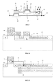
- FIG. 5 is a cross-sectional diagram of a first embodiment of the semiconductor photosensitive unit in the present invention as illustrated by the equivalent circuits in FIG. 3 and FIG. 4 .
- the semiconductor photosensitive unit of the present invention includes a doped well 301 of the second conductivity type formed in a semiconductor substrate 200 of the first conductivity type, and the semiconductor substrate 200 includes, but is not limited to, a silicon substrate, a germanium substrate, a silicon germanium substrate, or a silicon-on-insulator substrate; a diffusion region 304 and a photosensitive region 201 of the first conductivity type are disposed in the doped well 301 of the second conductivity type, a second current channel region is formed in the part of the semiconductor substrate between the diffusion region 304 and the photosensitive region 201 of the first conductivity type, and a third-layer insulation film 302 and a second control gate 303 are sequentially disposed on the second current channel region.
- the photosensitive region 201 of the first conductivity type and the doped well 301 of the second conductivity type form a photodiode for light sensing
- a pinning layer 202 of the second conductivity type is also disposed in the photosensitive region 201 of the first conductivity type, and the pinning layer 202 of the second conductivity type may be used for separating a light absorption region of the photodiode away from the disturbed surface of the semiconductor substrate 200
- a doped region 202 of the second conductivity type with high doping concentration is also disposed in the doped well 301 of the second conductivity type, and the doped region 202 of the second conductivity type is used for leading out a non-photosensitive region end of the photodiode and the doped well 301 of the second conductivity type to be connected to an external electrode.
- a first source 401 and a first drain 402 of the second conductivity type are further disposed in the semiconductor substrate 200 of the first conductivity type, a first current channel region is disposed in the part of the semiconductor substrate between the first source 401 and the first drain 402 of the second conductivity type, and the first current channel region, the first drain 402 and the first source 401 are isolated from the doped well 301 of the second conductivity type by a first insulation layer 300 in the semiconductor substrate 200 ; a first-layer insulation film 403 , a floating gate 404 of the first conductivity type, a second-layer insulation film 405 , and a first control gate 406 are sequentially disposed on the first current channel region; the floating gate 404 of the first conductivity type is electrically connected to the diffusion region 304 of the first conductivity type by an electrical connection line 400 .
- the first insulation layer 300 is a trench isolating structure having an insulating effect in the semiconductor substrate 200 , and its material is silicon nitride or silicon dioxide.
- the first conductivity type may be n-type or p-type; correspondingly, when the first conductivity type is n-type, the second conductivity type is p-type; and when the first conductivity type is p-type, the second conductivity type is n-type.
- the materials of the first-layer insulation film 403 , the second insulation film 405 and the third-layer insulation film 302 are respectively any of silicon dioxide, silicon nitride, silicon oxynitride, an insulating material of a high dielectric constant, or laminated layers of the above materials, wherein the insulating material of a high dielectric constant includes, but is not limited to, hafnium oxide, zirconium oxide or aluminum oxide.
- the material of the floating gate 404 of the first conductivity type may be silicon, germanium or silicon germanium, may be tungsten, titanium or titanium nitride, and may also be a mixed layer of a semiconductor material and a metallic material.
- the material of the first control gate 406 and the second control gate 303 may be a doped semiconductor material such as silicon, germanium or silicon germanium, may be a metallic material such as molybdenum, gold, titanium, tungsten, copper, or aluminum, and may also be a mixed layer of one or two types of metal compositions such as metal silicides or metal nitrides.
- the material of the electrical connection line 400 is a wire composed of one or more of a metal such as molybdenum, gold, titanium, tungsten, copper, or aluminum, a metal composition such as a metal nitride or a metal silicide, and a doped semiconductor material such as doped silicon, germanium or silicon germanium.
- a metal such as molybdenum, gold, titanium, tungsten, copper, or aluminum
- a metal composition such as a metal nitride or a metal silicide
- a doped semiconductor material such as doped silicon, germanium or silicon germanium.
- FIG. 6 is a cross-sectional diagram of a second embodiment of the semiconductor photosensitive unit in the present invention provided based on the two equivalent circuits of the semiconductor photosensitive unit in the present invention illustrated in FIG. 3 and FIG. 4 .
- the semiconductor photosensitive unit illustrated in FIG. 6 is an improvement to the structure of the semiconductor photosensitive unit illustrated in FIG. 5 .
- the floating gate 404 is electrically connected to the diffusion region 304 of the first conductivity type by the electrical connection line 400 , while in the semiconductor photosensitive unit illustrated in FIG.
- the floating gate 404 of the first conductivity type directly extends onto the diffusion region 304 of the first conductivity type and contacts the diffusion region 304 of the first conductivity type, such that the floating gate 404 of the first conductivity type is directly connected to the diffusion region 303 of the first conductivity type, whereby the manufacturing process of the semiconductor photosensitive unit can be simplified and the design difficulty of a peripheral circuit is reduced.
- FIG. 7 is a three-dimensional structural diagram of a third embodiment of the semiconductor photosensitive unit in the present invention provided based on the two equivalent circuits of the semiconductor photosensitive unit in the present invention illustrated in FIG. 3 and FIG. 4 .
- the semiconductor photosensitive unit illustrated in FIG. 7 is an improvement to the structure of the semiconductor photosensitive unit illustrated in FIG. 6 .
- the first current channel region and the second current channel region are of a parallel structure; while in the semiconductor photosensitive unit illustrated in FIG. 7 , the first current channel region and the second current channel region are of a vertical structure.
- FIG. 8 and FIG. 9 are two equivalent circuit diagrams of the semiconductor photosensitive unit in the present invention.
- the semiconductor photosensitive unit of the present invention includes the photodiode 20 , the gating MOS transistor 30 and the floating gate transistor 40 that are disposed in the semiconductor substrate of the first conductivity type, wherein the photodiode 20 includes the first end 21 of the first conductivity type and the second end 22 of the second conductivity type; the floating gate transistor 40 includes the first source 43 and the first drain 44 of the second conductivity type, the floating gate 42 of the first conductivity type that controls the switch-on or switch-off of the first current channel region between the first source 43 and the first drain 44 , and the first control gate 41 having a capacitive coupling effect on the floating gate 42 ; the gating MOS transistor 30 includes the second source 32 and the second drain 33 of the first conductivity type and the second control gate 31 for controlling the switch-on or switch-off of the second current channel region between the second source 32 and the second drain 33
- the gating MOS transistor is a PMOS transistor
- the second source 32 of the gating MOS transistor 30 is connected to the floating gate 42 of the floating gate transistor 40
- the second drain 33 of the gating MOS transistor 30 is connected to the anode of the photodiode 20
- the cathode of the photodiode 20 is connected to the first drain 44 of the floating gate transistor 40 , as shown in FIG. 8 .
- the gating MOS transistor is an NMOS transistor
- the second source 32 of the gating MOS transistor 30 is connected to the floating gate 42 of the floating gate transistor 40
- the second drain 33 of the gating MOS transistor 30 is connected to the cathode of the photodiode 20
- the anode of the photodiode 20 is connected to the first drain 44 of the floating gate transistor 40 , as shown in FIG. 9 .
- the two equivalent circuits of the semiconductor photosensitive unit in the present invention illustrated in FIG. 8 and FIG. 9 may be regarded as further improvements to the two equivalent circuits of the semiconductor photosensitive unit in the present invention illustrated in FIG. 3 and FIG. 4 .
- the direct connection of the second end 22 of the second conductivity type of the photodiode 20 to the first drain 44 of the first conductivity type of the floating gate transistor 40 can simplify the manufacturing process of the semiconductor photosensitive unit and reduce the design difficulty of a peripheral circuit.
- FIG. 10 is a cross-sectional diagram of a fourth embodiment of the semiconductor photosensitive unit in the present invention provided based on the two equivalent circuits of the semiconductor photosensitive unit in the present invention illustrated in FIG. 8 and FIG. 9 .
- the semiconductor photosensitive unit of the present invention includes the doped well 301 of the second conductivity type disposed in the semiconductor substrate 200 of the first conductivity type, the diffusion region 304 and the photosensitive region 201 of the first conductivity type are disposed in the doped well 301 of the second conductivity type, the second current channel region is disposed in the part of the semiconductor substrate between the diffusion region 304 and the photosensitive region 201 of the first conductivity type, and the third-layer insulation film 302 and the second control gate 303 are sequentially disposed on the second current channel region.
- the photosensitive region 201 of the first conductivity type and the doped well 301 of the second conductivity type form a photodiode for light sensing
- the pinning layer 202 of the second conductivity type is also disposed in the photosensitive region 201 of the first conductivity type
- the pinning layer 202 of the second conductivity type may be used for separating a light absorption region of the photodiode away from the disturbed surface of the semiconductor substrate 200 .
- the doped region 202 of the second conductivity type with high doping concentration is also disposed in the doped well 301 of the first conductivity type, and the doped region 202 of the second conductivity type is used for leading out a non-photosensitive region end of the photodiode and the doped well 301 of the second conductivity type to be connected to an external electrode.
- the first source 401 of the second conductivity type is further disposed in the semiconductor substrate 200 of the first conductivity type, the first current channel region is disposed in the part of the semiconductor substrate between the first source 401 of the second conductivity type and the doped well 301 of the second conductivity type, and the first-layer insulation film 403 , the floating gate 404 of the first conductivity type, the second-layer insulation film 405 , and the first control gate 406 are sequentially disposed on the first current channel region; the floating gate 404 of the first conductivity type extends out of the first-layer insulation film 403 onto the diffusion region 304 of the first conductivity type and contacts the diffusion region 303 of the first conductivity type, such that the floating gate 404 of the first conductivity type is connected to the diffusion region 304 of the first conductivity type.
- the first conductivity type may be n-type or p-type; correspondingly, when the first conductivity type is n-type, the second conductivity type is p-type; and when the first conductivity type is p-type, the second conductivity type is n-type.
- the materials of the first-layer insulation film 403 , the second insulation film 405 and the third-layer insulation film 302 are respectively one of silicon dioxide, silicon nitride, silicon oxynitride, an insulating material of a high dielectric constant, or laminated layers of the above materials, wherein the insulating material of a high dielectric constant includes, but is not limited to, hafnium oxide, zirconium oxide or aluminum oxide.
- the material of the floating gate 404 of the first conductivity type may be silicon, germanium or silicon germanium of the first conductivity type, may be tungsten, titanium or titanium nitride, and may also be a mixed layer of a semiconductor material and a metallic material.
- the material of the first control gate 406 and the second control gate 303 may be a doped semiconductor material such as doped silicon, germanium or silicon germanium, may be a metallic material such as molybdenum, gold, titanium, tungsten, copper, or aluminum, and may also be a mixed layer of one or two types of metal compositions such as metal silicides and metal nitrides.
- the floating gate 404 of the first conductivity type, the first control gate 406 and the second control gate 303 are all disposed on the surface of the semiconductor substrate 200 , such that the first current channel region controlled by the floating gate 404 of the first conductivity type and the second current channel region controlled by the second control gate 303 are both of a planar current channel structure.
- the floating gate 404 of the first conductivity type, the first control gate 406 and the second control gate 303 in the semiconductor photosensitive unit of the present invention may additionally be separately or together recessed in the semiconductor substrate 200 , thereby forming the first current channel region and the second current channel region of a recessed channel structure (also called a U-shaped channel structure) or a vertical channel structure.
- a recessed channel structure also called a U-shaped channel structure
- FIG. 11 is a cross-sectional diagram of a fifth embodiment of the semiconductor photosensitive unit in the present invention in which the second control gate 303 is recessed in the semiconductor substrate 200 and is applied in the semiconductor photosensitive unit illustrated in FIG. 5 .
- the second control gate 303 is recessed in the semiconductor substrate 200 , thereby forming the second current channel region of a U-shaped channel structure, such that with the same size of the semiconductor photosensitive unit, the length of the second current channel region between the diffusion region 304 and the photosensitive region 201 of the first conductivity type is prolonged to reduce the current leakage, and with the same length of the second current channel region, the size of the semiconductor photosensitive unit is reduced and the density of an image sensor chip is increased.
- FIG. 12 is a cross-sectional diagram of a sixth embodiment of the semiconductor photosensitive unit in the present invention in which the floating gate 404 of the first conductivity type is recessed in the semiconductor substrate 200 and is applied in the semiconductor photosensitive unit illustrated in FIG. 10 .
- the floating gate 404 of the first conductivity type is recessed in the semiconductor substrate 200 , thereby forming the first current channel region of a U-shaped channel structure, such that with the same size of the semiconductor photosensitive unit, the length of the first current channel region between the first source 401 and the doped well 201 of the second conductivity type is prolonged to reduce the current leakage and lower the power consumption of a chip.
- the depth of the doped well 301 of the second conductivity type may be increased to reduce the current leakage of a parasitic MOS transistor between the floating gate 404 of the first conductivity type and the semiconductor substrate 200 and prolong the charge storage time of the floating gate 404 of the first conductivity type; or with the same length of the first current channel region, the size of the semiconductor photosensitive unit is reduced and the density of an image sensor chip is increased.
- FIG. 13 is a cross-sectional diagram of a seventh embodiment of the semiconductor photosensitive unit in the present invention in which the first control gate 406 and the floating gate 404 of the first conductivity type are both recessed in the semiconductor substrate 200 and are applied in the semiconductor photosensitive unit illustrated in FIG. 10 . As shown in FIG.
- the first control gate 406 and the floating gate 404 of the first conductivity type are both recessed in the semiconductor substrate 200 , and the first drain 401 of the second conductivity type is disposed in the semiconductor substrate 200 at the bottom of the floating gate 404 and the first control gate 406 , thereby forming the current channel region of a vertical structure, such that with the same size of the semiconductor photosensitive unit, the length of the first current channel region between the first source 401 and the doped well 201 of the second conductivity type may be prolonged to reduce the current leakage and lower the power consumption of a chip, or with the same length of the first current channel region, the size of the semiconductor photosensitive unit is reduced and the density of an image sensor chip is increased.
- the first control gate 406 of the floating gate transistor has a capacitive coupling effect on the floating gate 404 of the first conductivity type, and to increase the capacitive coupling ratio of the first control gate 406 to the floating gate 404 of the first conductivity type, the first control gate 406 is disposed on the floating gate 404 of the first conductivity type and extends to one side of the floating gate 404 of the first conductivity type, such that the first control gate 406 covers the floating gate 404 on the top and one side of the floating gate 404 of the first conductivity type, thereby increasing the corresponding area of the first control gate 406 and the floating gate 404 and increasing the capacitive coupling ratio of the first control gate 406 to the floating gate 404 ;
- FIG. 14 illustrates a structural diagram that the first control gate 406 covers the floating gate 404 on the top and one side of the floating gate 404 .
- the first control gate 406 may also be disposed on the floating gate 404 of the first conductivity type and extend to two sides of the floating gate 404 of the first conductivity type, such that the first control gate 406 covers the floating gate 404 on the top and two sides of the floating gate 404 of the first conductivity type, thereby further increasing the corresponding area of the first control gate 406 and the floating gate 404 and increasing the capacitive coupling ratio of the first control gate 406 to the floating gate 404 ;
- FIG. 15 illustrates a structural diagram that the first control gate 406 covers the floating gate 404 on the top and two sides of the floating gate 404 .
- a semiconductor photosensitive unit array of the present invention may be formed by using multiple semiconductor photosensitive units of the present invention.
- FIG. 16 is an equivalent circuit diagram of a first embodiment of the semiconductor photosensitive unit array in the present invention. As shown in FIG. 16 , in this embodiment, the second end of the photodiode in each semiconductor photosensitive unit is not connected to the first drain of the floating gate transistor.
- the semiconductor photosensitive unit array of the present invention includes multiple source lines ( 1001 - 1 , 1001 - 2 , . . . , 1001 - x ), multiple word lines ( 1002 - 1 , 1002 - 2 , . . . , 1002 - x ), multiple selection lines ( 1003 - 1 , 1003 - 2 , . .
- any one of the source lines is connected to the first sources of the semiconductor photosensitive units
- any one of the word lines is connected to the first control gates of the semiconductor photosensitive units
- any one of the selection lines is connected to the second control gates of the semiconductor photosensitive units
- any one of the bit lines is connected to the second ends of the photodiodes of the semiconductor photosensitive units
- any one of the read lines is connected to the first drains of the semiconductor photosensitive units
- a combination of any one of the word lines and any one of the read lines corresponds to an individual semiconductor photosensitive unit, for example, a combination of a word line 1002 - x in the word lines and a read line 2002 - 1 in the read lines corresponds to an individual semiconductor photosensitive unit 3000 - x 1 .
- FIG. 17 is an equivalent circuit diagram of a second embodiment of the semiconductor photosensitive unit array in the present invention. As shown in FIG. 16 , in this embodiment, the second end of the photodiode in each semiconductor photosensitive unit is connected to the first drain of the floating gate transistor.
- the semiconductor photosensitive unit array of the present invention includes multiple source lines ( 1001 - 1 , 1001 - 2 , . . . , 1001 - x ), multiple word lines ( 1002 - 1 , 1002 - 2 , . . . , 1002 - x ), multiple selection lines ( 1003 - 1 , 1003 - 2 , . . .
- any one of the source lines is connected to the first sources of the semiconductor photosensitive units
- any one of the word lines is connected to the first control gates of the semiconductor photosensitive units
- any one of the selection lines is connected to the second control gates of the semiconductor photosensitive units
- any one of the bit lines is connected to the first drains of the semiconductor photosensitive units
- a combination of any one of the source lines and any one of the bit lines corresponds to an individual semiconductor photosensitive unit, for example, a combination of a word line 1002 - 1 in the word lines and a read line 2001 - 1 in the bit lines corresponds to an individual semiconductor photosensitive unit 4000 - 11 .
Landscapes
- Physics & Mathematics (AREA)
- Engineering & Computer Science (AREA)
- Power Engineering (AREA)
- Electromagnetism (AREA)
- Condensed Matter Physics & Semiconductors (AREA)
- General Physics & Mathematics (AREA)
- Computer Hardware Design (AREA)
- Microelectronics & Electronic Packaging (AREA)
- Solid State Image Pick-Up Elements (AREA)
Applications Claiming Priority (4)
| Application Number | Priority Date | Filing Date | Title |
|---|---|---|---|
| CN201410140574.9A CN104157658B (zh) | 2014-04-09 | 2014-04-09 | 一种半导体感光单元及其半导体感光单元阵列 |
| CN201410140574 | 2014-04-09 | ||
| CN201410140574.9 | 2014-04-09 | ||
| PCT/CN2015/076030 WO2015154657A1 (zh) | 2014-04-09 | 2015-04-08 | 一种半导体感光单元及其半导体感光单元阵列 |
Publications (2)
| Publication Number | Publication Date |
|---|---|
| US20170084648A1 US20170084648A1 (en) | 2017-03-23 |
| US9847362B2 true US9847362B2 (en) | 2017-12-19 |
Family
ID=51883120
Family Applications (1)
| Application Number | Title | Priority Date | Filing Date |
|---|---|---|---|
| US15/126,580 Active US9847362B2 (en) | 2014-04-09 | 2015-04-08 | Semiconductor photosensitive unit and semiconductor photosensitive unit array thereof |
Country Status (3)
| Country | Link |
|---|---|
| US (1) | US9847362B2 (zh) |
| CN (1) | CN104157658B (zh) |
| WO (1) | WO2015154657A1 (zh) |
Cited By (1)
| Publication number | Priority date | Publication date | Assignee | Title |
|---|---|---|---|---|
| US10644057B2 (en) | 2017-10-10 | 2020-05-05 | Omnivision Technologies, Inc. | Source follower contact |
Families Citing this family (25)
| Publication number | Priority date | Publication date | Assignee | Title |
|---|---|---|---|---|
| CN104157658B (zh) | 2014-04-09 | 2017-05-10 | 苏州东微半导体有限公司 | 一种半导体感光单元及其半导体感光单元阵列 |
| EP3227921B1 (en) * | 2014-12-03 | 2019-07-24 | Robert Bosch GmbH | Pixel structure for energy harvesting and image sensing |
| EP3363050B1 (en) | 2015-07-23 | 2020-07-08 | Artilux Inc. | High efficiency wide spectrum sensor |
| US10861888B2 (en) | 2015-08-04 | 2020-12-08 | Artilux, Inc. | Silicon germanium imager with photodiode in trench |
| US10761599B2 (en) | 2015-08-04 | 2020-09-01 | Artilux, Inc. | Eye gesture tracking |
| US10707260B2 (en) | 2015-08-04 | 2020-07-07 | Artilux, Inc. | Circuit for operating a multi-gate VIS/IR photodiode |
| WO2017024121A1 (en) | 2015-08-04 | 2017-02-09 | Artilux Corporation | Germanium-silicon light sensing apparatus |
| CN114754864B (zh) * | 2015-08-27 | 2023-03-24 | 光程研创股份有限公司 | 宽频谱光学传感器 |
| US10254389B2 (en) | 2015-11-06 | 2019-04-09 | Artilux Corporation | High-speed light sensing apparatus |
| US10418407B2 (en) | 2015-11-06 | 2019-09-17 | Artilux, Inc. | High-speed light sensing apparatus III |
| US10741598B2 (en) | 2015-11-06 | 2020-08-11 | Atrilux, Inc. | High-speed light sensing apparatus II |
| US10739443B2 (en) | 2015-11-06 | 2020-08-11 | Artilux, Inc. | High-speed light sensing apparatus II |
| US10886309B2 (en) | 2015-11-06 | 2021-01-05 | Artilux, Inc. | High-speed light sensing apparatus II |
| US11105928B2 (en) | 2018-02-23 | 2021-08-31 | Artilux, Inc. | Light-sensing apparatus and light-sensing method thereof |
| TWI788246B (zh) | 2018-02-23 | 2022-12-21 | 美商光程研創股份有限公司 | 光偵測裝置 |
| TWI780007B (zh) | 2018-04-08 | 2022-10-01 | 美商光程研創股份有限公司 | 光偵測裝置及其系統 |
| CN110387227B (zh) * | 2018-04-20 | 2021-03-05 | 京东方科技集团股份有限公司 | 钙钛矿薄膜、钙钛矿电致发光器件及制备方法、显示装置 |
| TWI795562B (zh) | 2018-05-07 | 2023-03-11 | 美商光程研創股份有限公司 | 雪崩式之光電晶體 |
| US10969877B2 (en) | 2018-05-08 | 2021-04-06 | Artilux, Inc. | Display apparatus |
| US10756129B2 (en) * | 2019-01-10 | 2020-08-25 | Semiconductor Components Industries, Llc | Image sensors having imaging pixels with ring-shaped gates |
| US11101389B2 (en) | 2019-02-21 | 2021-08-24 | Marvell Asia Pte, Ltd. | Dual-use semiconductor device for solar power and data storage |
| CN110323236A (zh) * | 2019-05-09 | 2019-10-11 | 德淮半导体有限公司 | 图像传感器及其形成方法 |
| CN110677604B (zh) * | 2019-10-12 | 2024-02-20 | 南京威派视半导体技术有限公司 | 电压域全局曝光图像传感器的像素单元及其控制方法 |
| US11183242B1 (en) * | 2020-05-18 | 2021-11-23 | Micron Technology, Inc. | Preventing parasitic current during program operations in memory |
| CN112864183B (zh) * | 2021-01-18 | 2023-08-25 | 上海集成电路装备材料产业创新中心有限公司 | 一种改善传输迟滞的像元结构 |
Citations (8)
| Publication number | Priority date | Publication date | Assignee | Title |
|---|---|---|---|---|
| US20020171102A1 (en) * | 2001-03-22 | 2002-11-21 | Fuji Photo Film Co., Ltd. | Non-volatile solid state image pickup device and its drive |
| JP2003333431A (ja) | 2002-05-14 | 2003-11-21 | Victor Co Of Japan Ltd | 固体撮像装置とその駆動方法 |
| CN1684261A (zh) | 2004-04-12 | 2005-10-19 | 硅存储技术公司 | 非易失存储单元阵列及其制造方法和操作方法 |
| US7091531B2 (en) | 2004-04-07 | 2006-08-15 | Micron Technology, Inc. | High dynamic range pixel amplifier |
| CN101237531A (zh) | 2006-11-13 | 2008-08-06 | 三星电子株式会社 | 互补金属氧化物半导体图像传感器像素电路及结构和操作 |
| CN101707202A (zh) | 2009-11-20 | 2010-05-12 | 苏州东微半导体有限公司 | 半导体感光器件及其制造方法和应用 |
| CN103594477A (zh) | 2013-11-06 | 2014-02-19 | 复旦大学 | 一种半导体感光器件及其制造方法 |
| CN104157658A (zh) | 2014-04-09 | 2014-11-19 | 苏州东微半导体有限公司 | 一种半导体感光单元及其半导体感光单元阵列 |
-
2014
- 2014-04-09 CN CN201410140574.9A patent/CN104157658B/zh active Active
-
2015
- 2015-04-08 US US15/126,580 patent/US9847362B2/en active Active
- 2015-04-08 WO PCT/CN2015/076030 patent/WO2015154657A1/zh active Application Filing
Patent Citations (8)
| Publication number | Priority date | Publication date | Assignee | Title |
|---|---|---|---|---|
| US20020171102A1 (en) * | 2001-03-22 | 2002-11-21 | Fuji Photo Film Co., Ltd. | Non-volatile solid state image pickup device and its drive |
| JP2003333431A (ja) | 2002-05-14 | 2003-11-21 | Victor Co Of Japan Ltd | 固体撮像装置とその駆動方法 |
| US7091531B2 (en) | 2004-04-07 | 2006-08-15 | Micron Technology, Inc. | High dynamic range pixel amplifier |
| CN1684261A (zh) | 2004-04-12 | 2005-10-19 | 硅存储技术公司 | 非易失存储单元阵列及其制造方法和操作方法 |
| CN101237531A (zh) | 2006-11-13 | 2008-08-06 | 三星电子株式会社 | 互补金属氧化物半导体图像传感器像素电路及结构和操作 |
| CN101707202A (zh) | 2009-11-20 | 2010-05-12 | 苏州东微半导体有限公司 | 半导体感光器件及其制造方法和应用 |
| CN103594477A (zh) | 2013-11-06 | 2014-02-19 | 复旦大学 | 一种半导体感光器件及其制造方法 |
| CN104157658A (zh) | 2014-04-09 | 2014-11-19 | 苏州东微半导体有限公司 | 一种半导体感光单元及其半导体感光单元阵列 |
Non-Patent Citations (1)
| Title |
|---|
| ISA/CN, International Search Report issued in PCT/CN2015/076030, dated Jul. 22, 2015, total 5 pages with English translation. |
Cited By (1)
| Publication number | Priority date | Publication date | Assignee | Title |
|---|---|---|---|---|
| US10644057B2 (en) | 2017-10-10 | 2020-05-05 | Omnivision Technologies, Inc. | Source follower contact |
Also Published As
| Publication number | Publication date |
|---|---|
| WO2015154657A1 (zh) | 2015-10-15 |
| US20170084648A1 (en) | 2017-03-23 |
| CN104157658B (zh) | 2017-05-10 |
| CN104157658A (zh) | 2014-11-19 |
Similar Documents
| Publication | Publication Date | Title |
|---|---|---|
| US9847362B2 (en) | Semiconductor photosensitive unit and semiconductor photosensitive unit array thereof | |
| CN101707202B (zh) | 半导体感光器件及其制造方法和应用 | |
| US10971533B2 (en) | Vertical transfer gate with charge transfer and charge storage capabilities | |
| US9942506B2 (en) | Solid-state imaging device | |
| US8513761B2 (en) | Backside illumination semiconductor image sensor | |
| TWI816151B (zh) | Cmos影像感測器中抑制浮動擴散接面洩漏之隔離結構及其製造方法 | |
| US10741600B2 (en) | Imaging device including semiconductor substrate and pixel | |
| TWI762373B (zh) | 像素陣列及在半導體基板中製造像素陣列之方法 | |
| US11264419B2 (en) | Image sensor with fully depleted silicon on insulator substrate | |
| US9887234B2 (en) | CMOS image sensor and method for forming the same | |
| US20140077067A1 (en) | Solid-state imaging device | |
| KR100790586B1 (ko) | Cmos 이미지 센서 액티브 픽셀 및 그 신호 감지 방법 | |
| US9590127B2 (en) | Dual conversion gain image sensor cell | |
| US11860033B2 (en) | Photodetector, photodetector array, and drive method comprising a second transistor including a channel of first conductivity type and a first transistor including a channel of second conductivity type that has polarity opposite to polarity of the first conductivity type | |
| KR20200040516A (ko) | 이미지 센서 | |
| KR970076857A (ko) | 셀의 포토다이오드를 리셋하기 위하여 기생 트랜지스터를 사용하는 액티브 화소 감지셀 | |
| CN102347337A (zh) | 背面照光的cmos图像传感器 | |
| CN101715041A (zh) | 半导体感光器件的控制方法 | |
| US8809913B2 (en) | Pixel architecture and method | |
| CN116435323A (zh) | Cmos图像传感器及其形成方法 | |
| KR100790585B1 (ko) | Cmos 이미지 센서 픽셀 및 그 신호 감지 방법 | |
| KR20150019887A (ko) | 소스 팔로워를 포함하는 이미지 센서 | |
| US20150021668A1 (en) | Photosensitive cell of an image sensor | |
| US20190393253A1 (en) | Image sensor | |
| CN102315231A (zh) | 一种半导体感光器件及其制造方法 |
Legal Events
| Date | Code | Title | Description |
|---|---|---|---|
| AS | Assignment |
Owner name: SU ZHOU ORIENTAL SEMICONDUCTOR CO., LTD., CHINA Free format text: ASSIGNMENT OF ASSIGNORS INTEREST;ASSIGNORS:LIU, WEI;LIU, LEI;WANG, PENGFEI;REEL/FRAME:039761/0286 Effective date: 20160912 |
|
| AS | Assignment |
Owner name: SU ZHOU ORIENTAL SEMICONDUCTOR CO., LTD., CHINA Free format text: CHANGE OF ASSIGNEE'S ADDRESS;ASSIGNOR:SU ZHOU ORIENTAL SEMICONDUCTOR CO., LTD.;REEL/FRAME:043971/0973 Effective date: 20170829 |
|
| STCF | Information on status: patent grant |
Free format text: PATENTED CASE |
|
| MAFP | Maintenance fee payment |
Free format text: PAYMENT OF MAINTENANCE FEE, 4TH YR, SMALL ENTITY (ORIGINAL EVENT CODE: M2551); ENTITY STATUS OF PATENT OWNER: SMALL ENTITY Year of fee payment: 4 |