US9830675B2 - Image-processing apparatus - Google Patents
Image-processing apparatus Download PDFInfo
- Publication number
- US9830675B2 US9830675B2 US15/000,589 US201615000589A US9830675B2 US 9830675 B2 US9830675 B2 US 9830675B2 US 201615000589 A US201615000589 A US 201615000589A US 9830675 B2 US9830675 B2 US 9830675B2
- Authority
- US
- United States
- Prior art keywords
- data
- image data
- row
- offset
- memory
- Prior art date
- Legal status (The legal status is an assumption and is not a legal conclusion. Google has not performed a legal analysis and makes no representation as to the accuracy of the status listed.)
- Active, expires
Links
Images


Classifications
-
- G—PHYSICS
- G06—COMPUTING; CALCULATING OR COUNTING
- G06T—IMAGE DATA PROCESSING OR GENERATION, IN GENERAL
- G06T1/00—General purpose image data processing
- G06T1/0007—Image acquisition
-
- G—PHYSICS
- G06—COMPUTING; CALCULATING OR COUNTING
- G06T—IMAGE DATA PROCESSING OR GENERATION, IN GENERAL
- G06T1/00—General purpose image data processing
- G06T1/60—Memory management
Definitions
- the present invention relates to an image-processing apparatus.
- An image is divided into a plurality of regions each having any size, and positions corresponding to regions between a plurality of different images are determined based on motion vector information to perform image processing.
- a method of segmenting partial image data of a rectangular region from image data to transfer the segmented partial image data when the image data is transferred from a memory storing the image data to an image-processing block.
- a method of reducing the number of transferring actions is disclosed in the publication of Japanese Unexamined Patent Application, First Publication No. 2004-127093.
- a portion of data of continuous addresses from a 1 st address (an address of data of an upper-left corner of a rectangular region) of partial image data of the rectangular region to a last address (an address of data of a lower-right corner of the rectangular region) in a memory is read.
- data may be read from the memory over a boundary of data capable of being accessed through one access to the memory.
- the boundary of the data capable of being accessed through the one access is referred to as an access boundary.
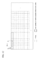
- FIGS. 12 and 13 illustrate a state of image data stored in the memory.
- a small rectangle indicates a pixel.
- an amount of data of one pixel is 8 bits.
- An amount of data capable of being accessed through the one access to the memory is 32 bits. That is, it is possible to access data of four pixels through one access to the memory and transfer the data.
- a boundary of a region of four pixels in a horizontal direction is an access boundary. The access boundary appears every four pixels in the horizontal direction.
- access boundaries B 200 , B 201 , B 202 , and B 203 are illustrated.
- image data IMG 200 and image data IMG 205 of rectangular regions are illustrated.
- Image data IMG 200 and the image data IMG 205 are constituted of data of six rows and data of each row is constituted of data of four pixels.
- the image data IMG 200 is in contact with the access boundary B 200 .
- data crossing the access boundary B 200 is not read from the memory. That is, the data of each row of the image data IMG 200 is read from the memory through one access to the memory.
- the data of each row of the image data IMG 200 is transferred from the memory through one burst transfer.
- the access boundary B 202 is located inside the image data IMG 205 . That is, data of one row of the image data IMG 205 is stored in the memory crossing access boundary B 202 . When data of one row of the image data IMG 205 is transferred, data crossing the access boundary B 202 is read from the memory. Thus, two accesses to the memory are necessary to transfer data of one row of the image data IMG 205 . Data of each row of the image data IMG 205 is transferred from the memory through two burst transfers. Therefore, the number of transfers when the image data IMG 205 is transferred is twice the number of transfers when the image data IMG 200 is transferred.
- an image-processing apparatus includes: a memory in which first image data is recorded, wherein the first image data includes second image data of a rectangular region; an offset-calculating block configured to calculate an offset for reading transfer data from the memory without crossing an access boundary in at least one row when transfer data to be transferred through a burst transfer among the second image data is read from the memory for each row, wherein an amount of position gap between a storage area of data of a first row of the first image data and a storage area of data of a second row adjacent to the first row includes the offset in the memory and wherein the access boundary is a boundary of data capable of being accessed through one access to the memory; a write block configured to write the first image data to the memory through a bus; a write control block configured to generate a write address of the first image data based on the offset calculated by the offset-calculating block and control the write block based on the generated write address; a read block configured to read the second image data from the memory through the bus; a read control block
- the offset-calculating block may calculate the offset based on an amount of data capable of being accessed through one access to the memory, an amount of data of one pixel, and a horizontal size of the rectangular region.
- the offset-calculating block may calculate the number of pixels per access by dividing the amount of data capable of being accessed through the one access to the memory by the amount of data of the one pixel, the offset-calculating block may calculate the minimum number of accesses necessary to transfer data of the horizontal size by dividing the horizontal size of the rectangular region by the number of pixels per access, the offset-calculating block may calculate a third value by adding 1 to a second value obtained by subtracting the horizontal size of the rectangular region from a first value obtained by multiplying the minimum number of accesses by the number of pixels per access, and calculate a fourth value by dividing the number of pixels per access by the third value, wherein the fourth value is the number of rows necessary to generate a row in which the transfer data does not cross a boundary of the address when the transfer data is read from the memory, and the offset-calculating block may calculate the offset of each row by dividing the number of pixels per access by the fourth value.
- the offset may be less than an amount of data capable of being transferred through one transfer.
- the offset of each row may be a fixed value.
- FIG. 1 is a block diagram illustrating a configuration of an imaging apparatus of an embodiment of the present invention.
- FIG. 2 is a reference diagram illustrating positions of image data in a memory in an embodiment of the present invention.
- FIG. 3 is a reference diagram illustrating positions of image data in a memory in an embodiment of the present invention.
- FIG. 4 is a reference diagram illustrating positions of image data in a memory in an embodiment of the present invention.
- FIG. 5 is a flowchart illustrating a procedure of an operation of an offset-calculating block of an embodiment of the present invention.
- FIG. 6 is a reference diagram illustrating types of accesses to a memory of an embodiment of the present invention.
- FIG. 7 is a reference diagram illustrating a relationship between a position of a 1 st pixel of a rectangular region and the number of accesses in a memory of an embodiment of the present invention.
- FIG. 8 is a reference diagram illustrating a given offset in an embodiment of the present invention.
- FIG. 9 is a reference diagram illustrating positions of image data in a memory in an embodiment of the present invention.
- FIG. 10 is a reference diagram illustrating positions of image data in a memory in an embodiment of the present invention.
- FIG. 11 is a reference diagram illustrating positions of image data in a memory in an embodiment of the present invention.
- FIG. 12 is a reference diagram illustrating positions of image data in a memory in a conventional technology.
- FIG. 13 is a reference diagram illustrating positions of image data in a memory in the conventional technology.
- FIG. 14 is a reference diagram illustrating positions of image data in a memory in the conventional technology.
- FIG. 15 is a reference diagram illustrating positions of image data in a memory in the conventional technology.
- FIG. 16 is a reference diagram illustrating positions of image data in a memory in the conventional technology.
- FIG. 17 is a reference diagram illustrating positions of image data in a memory in the conventional technology.
- FIG. 18 is a reference diagram illustrating positions of image data in a memory in the conventional technology.
- FIG. 19 is a reference diagram illustrating positions of image data in a memory in the conventional technology.
- FIG. 1 is a block diagram illustrating a configuration of an imaging apparatus 100 of the embodiment of the present invention.
- the imaging apparatus 100 includes an image sensor 1 , a preprocessing block 2 , an image-processing block 3 , a display-processing block 4 , a display device 5 , a central processing unit (CPU) 6 , a memory 7 , a media interface (I/F) 8 , a recording medium 9 , and a bus 10 .
- the preprocessing block 2 , the image-processing block 3 , and the memory 7 constitute an image-processing unit 110 .
- the preprocessing block 2 includes a write control block 20 and a write block 21 .
- the image-processing block 3 includes an offset-calculating block 30 , a read control block 31 , a read block 32 , a write control block 33 , and a write block 34 .
- the image sensor 1 is a charge-coupled device (CCD) or a complementary metal oxide semiconductor (CMOS) image sensor or the like.
- the image sensor 1 generates image data.
- the preprocessing block 2 performs preprocessing such as flaw correction or shading correction on image data output from the image sensor 1 .
- the image data processed by the preprocessing block 2 is stored in the memory 7 .
- the image-processing block 3 reads the image data from the memory 7 and performs image processing on the read image data. Thereby, the image-processing block 3 generates display image data or record image data.
- the generated display image data or the record image data is stored in the memory 7 .
- the display-processing block 4 acquires the display image data from the memory 7 .
- the display-processing block 4 performs display processing such as on-screen display (OSD) superimposition processing on the display image data.
- the display image data processed by the display-processing block 4 is output to the display device 5 .
- the display device 5 is a display device such as a thin film transistor (TFT) or an organic electroluminescence (EL) display.
- TFT thin film transistor
- EL organic electroluminescence
- the CPU 6 performs overall control of the imaging apparatus 100 .
- the memory 7 records image data or necessary data or information such as motion vector information.
- the image data is recorded to the memory 7 .
- the image data (first image data) includes image data (second image data which is hereinafter referred to as partial image data) of a rectangular region.
- the partial image data is a part of the entire image data stored in the memory 7 . That is, the number of pixels of the partial image data is less thin the total number of image data pixels.
- the partial image data includes data of at least two rows. When the image data is transferred from the memory 7 , one burst transfer is performed through one access to the memory 7 .
- the media I/F 8 acquires record image data from the memory 7 and records the record image data to the recording medium 9 . In addition, the media I/F 8 acquires the record image data from the recording medium 9 and transfers the record image data to the memory 7 .
- the recording medium 9 records the necessary data or information.
- the bus 10 transmits data, a command, etc.
- the preprocessing block 2 has a preprocessing circuit which performs preprocessing and includes the write control block 20 and the write block 21 . Illustration of the preprocessing circuit is omitted in FIG. 1 .
- the image-processing block 3 has an image-processing circuit and includes the offset-calculating block 30 , the read control block 31 , the read block 32 , the write control block 33 , and the write block 34 . The illustration of the image-processing circuit is omitted in FIG. 1 .
- the offset-calculating block 30 calculates an offset for reading transfer data from the memory 7 without crossing an access boundary in at least one row when the transfer data to be transferred through a burst transfer among the partial image data (second image data) is read from the memory 7 for each row.
- an amount of position gap between a storage area of data of a 1 st row of the image data and a storage area of data of a 2 nd row adjacent to the 1 st row includes the offset.
- the access boundary is a boundary of data capable of being accessed through one access to the memory 7 .
- the write block 21 writes the image data (first image data) to the memory 7 through the bus 10 .
- the write control block 20 generates a write address of the image data (first image data) based on the offset calculated by the offset-calculating block 30 and controls the write block 21 based on the generated write address
- the read block 32 reads the partial image data (second image data) from the memory 7 through the bus 10 .
- the read control block 31 generates a read address of the partial image data (second image data) based on the offset calculated by the offset-calculating block 30 and controls the read block 32 based on the generated read address.
- the write block 34 writes the partial image data (second image data) to the memory 7 through the bus 10 .
- the write control block 33 generates a write address of the partial image data (second image data) based on the offset calculated by the offset-calculating block 30 and controls the write block 34 based on the generated write address.
- a size of the partial image data (second image data) read from the memory 7 may not be the same as a size of the partial image data processed by the image-processing block 3 and written to the memory 7 .
- the image-processing block 3 performs image processing on the partial image data read by the read block 32 .
- the image-processing block 3 performs at least one of noise elimination, a YC conversion process, a resizing process, and a compression process. This image processing is performed by the image-processing circuit.
- the write block 34 writes the image data on which the image processing is performed to the memory 7 .
- FIGS. 14 and 15 illustrate positions of image data in a memory in a conventional technology.
- a leftmost number denotes an address.
- 32-bit data can be stored at one address of the memory.
- Data of one pixel is constituted of 8 bits.
- little-endian which is one data storage scheme, data is stored in sequence from a lower-order bit of each address.
- address 0 data of four pixels from a 1 st pixel to a 4 th pixel is stored.
- address 1 data of four pixels from a 5 th pixel to an 8 th pixel is stored.
- address 2 data of four pixels from a 9 th pixel to a 12 th pixel is stored.
- FIG. 15 illustrates positions of data of pixels on a memory.
- positions of image data constituted of data of five rows are illustrated.
- a leftmost number denotes a row number.
- a number written to the right, of the row number denotes an address at which data of a 1 st pixel of each row is stored.
- Data of each row is constituted of data of 18 pixels. Numbers of 1 to 18 denote data of pixels of each row. Numbers of 0 to 24 written every four pixels denote addresses.
- data of pixels is adjacent on an address space of the memory. Data of 17 th and 18 th pixels of each row is stored at addresses 4 , 9 , 14 , 19 , and 24 , respectively.
- the data of the 17 th and 18 th pixels is stored in lower-order bits.
- unnecessary data is stored in higher-order bits.
- Data of a last pixel of each row and data of a 1 st pixel of a row following each row are stored at continuous addresses. For example, data of an 18 th pixel of a 1 st row is stored at address 4 . Data of a 1 st pixel of a 2 nd row is stored at address 5 . Addresses 4 and 5 are continuous.
- a position at which data of a 1 st pixel of each row is stored is a position next to a position at which unnecessary data subsequent to data of a last pixel of a previous row is stored.
- a position at which data of a last pixel of each row is stored is not a last position of the address, unnecessary data is stored so that the address is filled with data.
- data of each row is constituted of data of 18 pixels
- data of a last pixel of each row is stored at a 2 nd position of the address.
- Unnecessary data is stored at 3 rd and 4 th positions of the address.
- Data of a last pixel of the 1 st row is stored at a 2 nd position of address 4 .
- Unnecessary data is stored at 3 rd and 4 th positions of address 4 .
- Data of a 1 st pixel of a 2 nd row is stored at a 1 st position of address 5 .
- Data of a last pixel of the 2 nd row is stored at a 2 nd position of address 9 .
- Unnecessary data is stored at 3 rd and 4 th positions of address 9 .
- Data of a 1 st pixel of a 3 rd row is stored at a 1 st position of address 10 .
- Data of a last pixel of the 3 rd row is stored at a 2 nd position of address 14 .
- Unnecessary data is stored in 3 rd and 4 th positions of address 14 .
- Data of a 1 st pixel of a 4 th row is stored at a 1 st position of address 15 .
- Data of a last pixel of the 4 th row is stored at a 2 nd position of address 19 .
- Unnecessary data is stored at 3 rd and 4 th positions of address 19 .
- Data of a 1 st pixel of a 5 th row is stored at a 1 st position of address 20 .
- Data of a last pixel of the 5 th row is stored at a 2 nd position of address 24 .
- Unnecessary data is stored at 3 rd and 4 th positions of address 24 .
- an amount of data of one pixel is 8 bits.
- An amount of data capable of being accessed through the one access to the memory is 32 bits. That is, it is possible to access data of four pixels through one access to the memory and transfer the data.
- a boundary of a region of four pixels in the horizontal direction is an access boundary. The access boundary appears every four pixels in the horizontal direction. In FIG. 15 , the access boundary matches an address boundary.
- Image data IMG 210 and the image data IMG 215 are illustrated.
- Image data IMG 210 and the image data IMG 215 are constituted of data of four rows, and data of each row is constituted of data of three pixels.
- Data of each row of the image data IMG 210 is constituted of data of 7 th to 9 th pixels in data of 1 st to 4 th rows of image data of 18 pixels ⁇ 5 rows.
- Data of each row of the image data IMG 215 is constituted of data of 14 th to 16 th pixels in the data of the 1 st to 4 th rows of the image data of 18 pixels ⁇ 5 rows.
- Data of the 1 st row of the image data IMG 210 is stored at addresses 1 and 2 .
- Data of the 2 nd row of the image data IMG 210 is stored at addresses 6 and 7 .
- Data of the 3 rd row of the image data IMG 210 is stored at addresses 11 and 12 .
- Data of the 4 th row of the image data IMG 210 is stored at addresses 16 and 17 . That is, an access boundary is inside a region in which data of each row is stored with respect to all the rows of the image data IMG 210 . In FIG. 15 , an access boundary is between a position at which data of the 8 th pixel of each row of the image data of 18 pixels ⁇ 5 rows is stored and a position at which data of the 9 th pixel is stored.
- data of all rows of the image data IMG 210 is read from the memory crossing access boundary.
- no access boundary is inside a region in which data of each row is stored with respect to all rows of the image data IMG 215 .
- data of all rows of the image data IMG 215 is read from the memory without crossing the access boundary.
- the access boundary may be included according to a position of partial image data in the memory.
- an access boundary is in a region in which data of each row is stored with respect to all rows of the partial image data (for example, the image data IMG 210 ).
- FIG. 2 illustrates positions of data of pixels on the memory 7 in the embodiment of the present invention.
- positions of image data constituted of data of five rows are illustrated.
- a leftmost number denotes a row number.
- a number written to the right of the row number denotes an address at which data of a 1 st pixel of each row is stored.
- Data of each row is constituted of data of 18 pixels.
- Numbers of 1 to 18 denote data of pixels of each row.
- data of pixels is adjacent on an address space of the memory 7 .
- a position at which the data of the 1 st pixel of each row is stored is at the distance of an offset from a position next to a position at which unnecessary data that is subsequent to data of a last pixel of the previous row is stored.
- unnecessary data of two pixels is stored after data of a last pixel of each row.
- the offset of each row is indicated by an arrow.
- the offset of each row corresponds to two pixels. Unnecessary data is stored in the region of the offset.
- Data of a last pixel of a 1 st row is stored at a 2 nd position of address 4 .
- Unnecessary data is stored at 3 rd and 4 th positions of address 4 .
- Data of a 1 st pixel of a 2 nd row is stored at a position at the distance two pixels from a 1 st position of address 5 , that is, a 3 rd position of address 5 .
- Data of a last pixel of the 2 nd row is stored at a last position of address 9 .
- Unnecessary data is stored at 1 st and 2 nd positions of address 10 .
- Data of a 1 st pixel of a 3 rd row is stored at a position at the distance of two pixels from a 3 rd position of address 10 , that is, a 1 st position of address 11 .
- Data of a last pixel of the 3 rd row is stored at a 2 nd position of address 15 .
- Unnecessary data is stored at 3 rd and 4 th positions of address 15 .
- Data of a 1 st pixel of a 4 th row is stored at a position at the distance of two pixels from a 1 st position of address 16 , that is, a 3 rd position of address 16 .
- Data of a last pixel of the 4 th row is stored at a last position of address 20 .
- Unnecessary data is stored at 1 st and 2 nd positions of address 21 .
- Data of a 1 st pixel of a 5 th row is stored at a position at the distance of two pixels from a 3 rd position of address 21 , that is, a 1 st position of address 22 .
- Data of a last pixel of the 5 th row is stored at a 2 nd position of address 26 .
- Unnecessary data is stored at 3 rd and 4 th positions of address 26 .
- the offset-calculating block 30 calculates the above-described offset.
- the offset is less than an amount of data (the number of pixels) capable of being accessed through one access to the memory 7 , that is, an amount of data (the number of pixels) capable of being transferred through one transfer.
- FIG. 2 it is possible to access data of four pixels through one access to the memory 7 and transfer the data.
- a boundary of a region of four pixels in the horizontal direction is an access boundary.
- the access boundary appears every four pixels in the horizontal direction.
- the access boundary matches an address boundary.
- Image data IMG 100 and the image data IMG 105 are illustrated.
- Image data IMG 100 and the image data IMG 105 are constituted of data of four rows, and data of each row is constituted of data of three pixels.
- Data of each row of the image data IMG 100 is constituted of data of 7 th to 9 th pixels in data of 1 st to 4 th rows of image data of 18 pixels ⁇ 5 rows.
- Data of each row of the image data IMG 105 is constituted of data of 14 th to 16 th pixels in data of the 1 st to 4 th rows of the image data of 18 pixels ⁇ 5 rows.
- Data of the 1 st row of the image data IMG 100 is stored at addresses 1 and 2 .
- Data of the 2 nd row of the image data IMG 100 is stored at address 7 .
- Data of the 3 rd row of the image data IMG 100 is stored at addresses 12 and 13 .
- Data of the 4 th row of the image data IMG 100 is stored at address 18 . That is, an access boundary is inside a region in which data of each row is stored with respect to some rows of the image data IMG 100 . In FIG. 2 , an access boundary is inside a region in which the data of the 1 st and 3 rd rows of the image data IMG 100 is stored.
- Data of the 1 st row of the image data IMG 105 is stored at address 3 .
- Data of the 2 nd row of the image data IMG 105 is stored at addresses 8 and 9 .
- Data of the 3 rd row of the image data IMG 105 is stored at address 14 .
- Data of the 4 th row of the image data IMG 105 is stored at addresses 19 and 20 . That is, an access boundary is inside a region in which data of each row is stored with respect to some rows of the image data IMG 105 . In FIG. 2 , an access boundary is inside a region in which the data of the 2 nd and 4 th rows of the image data IMG 105 is stored.
- the image data IMG 215 illustrated in FIG. 15 When the image data IMG 215 illustrated in FIG. 15 is transferred from the memory, one data transfer occurs every row. Accordingly, four data transfers occur for the entire image data IMG 215 .
- the image data IMG 105 illustrated in FIG. 2 is transferred from the memory 7 , one data transfer occurs in the 1 st and 3 rd rows and two data transfers occur in the 2 nd and 4 th rows. Accordingly, six data transfers occur for the entire image data IMG 105 .
- the number of transfers when the image data IMG 105 is transferred is greater than the number of transfers when the image data IMG 215 is transferred. As described above, the number of transfers of the partial image data may be greater than the number of transfers in the conventional technology. However, regardless of a position of a rectangular region, the number of transfers of the partial image data is less than the number of transfers in the worst state.
- a row in which there is an offset need not be all rows from which data of a 1 st row of partial image data is excluded.
- the offset may be in only some rows from which the data of the 1 st row of the partial image data is excluded.
- the offset need not be the same in all rows.
- an offset of each row is a fixed value, it is possible to easily calculate the offset.
- the offset is less than an amount of data capable of being transferred through one transfer here, the offset may be greater than the amount of data capable of being transferred through the one transfer.
- the offset of each row is a fixed value and corresponds to one pixel.
- FIG. 16 illustrates positions of image data in a memory in the conventional technology.
- a leftmost number denotes a row number.
- An uppermost number denotes the number of pixels.
- a boundary of a region of six pixels in the horizontal direction is an access boundary.
- the access boundary appears every six pixels in the horizontal direction.
- the access boundary matches an address boundary.
- an access boundary B 210 and an access boundary B 211 are illustrated.
- Image data IMG 220 and the image data IMG 225 are illustrated.
- Image data IMG 220 and the image data IMG 225 are constituted of data of eight rows, and data of each row is constituted of data of three pixels.
- No access boundary is inside a region in which data of each row is stored with respect to all rows of the image data IMG 220 .
- data of all the rows of the image data IMG 220 is read from the memory without crossing the access boundary.
- the access boundary B 211 is inside a region in which data of each row is stored with respect to all rows of the image data IMG 225 .
- the image data IMG 225 is transferred from the memory data of all the rows of the image data IMG 225 is read from the memory crossing the access boundary.
- FIG. 3 illustrates positions of image data on the memory 7 in the embodiment of the present invention.
- a leftmost number denotes a row number.
- An uppermost number denotes the number of pixels.
- a boundary of a region of six pixels in the horizontal direction is an access boundary. The access boundary appears every six pixels in the horizontal direction.
- the access boundary matches an address boundary.
- an access boundary B 100 an access boundary B 101 , and an access boundary B 102 are illustrated.
- an offset of each row corresponds to one pixel.
- image data IMG 110 and image data IMG 115 are illustrated.
- Image data IMG 110 and the image data IMG 115 are constituted of data of eight rows, and data of each row is constituted of data of three pixels.
- An access boundary is inside a region in which data of each row is stored with respect to some rows of the image data IMG 110 .
- an access boundary is inside a region in which data of 5 th and 6 th rows of the image data IMG 110 is stored.
- An access boundary is inside a region in which data of each row is stored with respect to some rows of the image data IMG 115 .
- an access boundary is inside a region in which data of 1 st , 2 nd , 7 th , and 8 th rows of the image data IMG 115 is stored.
- a size of a rectangular region in the vertical direction be less than an amount of data capable of being accessed through one access to the memory 7 , that is, an amount of data capable of being transferred through one transfer.
- the number of rows of the rectangular region is 8 and an amount of data, capable of being transferred through one transfer is 3.
- no access boundary is inside a region in which data of at least one row of eight rows constituting the partial image data is stored.
- the offset-calculating block 30 calculates an offset based on an amount of data capable of being accessed through one access to the memory 7 and an amount of data of one pixel.
- the offset of each row is a fixed value.
- FIG. 17 illustrates positions of image data in a memory in the conventional technology.
- a leftmost number denotes a row number.
- An uppermost number denotes the number of pixels.
- a boundary of a region of six pixels in the horizontal direction is an access boundary. The access boundary appears every six pixels in the horizontal direction. In FIG. 17 , the access boundary matches an address boundary.
- access boundaries B 220 and B 221 are illustrated.
- Image data IMG 230 and the image data IMG 235 are illustrated.
- Image data IMG 230 and the image data IMG 235 are constituted of data of four rows, and data of each row is constituted of data of three pixels.
- No access boundary is inside a region in which data of each row is stored with respect to all rows of the image data IMG 230 .
- data of all rows of the image data IMG 230 is read from the memory without crossing the access boundary.
- the access boundary B 221 is inside a region in which data of each row is stored with respect to all rows of the image data IMG 235 .
- the image data IMG 235 is transferred from the memory data of all the rows of the image data IMG 235 is read from the memory crossing the access boundary.
- FIG. 4 illustrates positions of image data on the memory 7 in the embodiment of the present invention.
- a leftmost number denotes a row number.
- An uppermost number denotes the number of pixels.
- a boundary of a region of six pixels in the horizontal direction is an access boundary. The access boundary appears every six pixels in the horizontal direction.
- the access boundary matches an address boundary.
- an access boundary B 110 , an access boundary B 111 , an access boundary B 112 , and an access boundary B 113 are illustrated.
- an offset of each row corresponds to three pixels.
- image data IMG 120 and image data IMG 125 are illustrated.
- Image data IMG 120 and the image data IMG 125 are constituted of data of four rows, and data of each row is constituted of data of three pixels.
- No access boundary is inside a region in which data of each row is stored with respect to all rows of the image data IMG 120 .
- An access boundary is inside a region in which data of each row is stored with respect to some rows of the image data IMG 125 .
- an access boundary is inside a region in which the data of the 1 st and 3 rd rows of the image data IMG 125 is stored.
- the offset-calculating block 30 calculates an offset by dividing half of an amount of data capable of being accessed through one access to the memory 7 , that is, an amount of data capable of being transferred through one transfer, by an amount of data of one pixel.
- an amount, of data capable of being transferred through one transfer is an amount of data of six pixels.
- the offset corresponds to three pixels.
- a size of a rectangular region the horizontal direction be less than or equal to half of an amount of data capable of being accessed through one access to the memory 7 , that is, an amount of data capable of being transferred through one transfer.
- the offset-calculating block 30 calculates an offset based on an amount of data capable of being accessed through one access to the memory 7 , an amount of data of one pixel, and a horizontal size of the rectangular region.
- FIG. 5 illustrates a procedure of an operation of the offset-calculating block 30 .
- the operation of the offset-calculating block 30 will be described.
- the following information is output from the CPU 6 to the offset-calculating block 30 .
- the data amount of the one access is an amount of data to be accessed through one access to the memory 7 .
- the offset-calculating block 30 calculates the offset according to the procedure illustrated in FIG. 5 based on the above-described information.
- the offset-calculating block 30 calculates the number of pixels A_pix per access by dividing the data amount A_data of one access by the data amount P_data of one pixel.
- the offset-calculating block 30 calculates a minimum value of the number of accesses when data of one row of the rectangular region is transferred (step S 110 ).
- FIG. 6 illustrates types of accesses to the memory 7 . In FIG. 6 , an access boundary in the memory 7 and data of one row of the rectangular region to be accessed are illustrated. A width between two adjacent access boundaries is the same as the number of pixels A_pix per access.
- the horizontal size H_pix of the rectangular region is less than or equal to the number of pixels A_pix (H_pix ⁇ A_pix) per access.
- access A 11 an access boundary is not included in a region to be accessed. That is, in access A 11 , transfer data is read from the memory 7 without crossing the access boundary.
- access A 11 the memory 7 is accessed once.
- one access boundary is included in the region to be accessed. That is, in access A 12 , transfer data is read from the memory 7 while crossing the access boundary once.
- the memory 7 is accessed twice.
- the horizontal size H_pix of the rectangular region is greater than the number of pixels A_pix per access, and the horizontal size H_pix of the rectangular region is less than or equal to twice the number of pixels A_pix per access (A_pix ⁇ H_pix ⁇ 2 ⁇ A_pix).
- access A 21 an access boundary is included in a region to be accessed. That is, in access A 21 , transfer data is read from the memory 7 while crossing the access boundary once.
- the memory 7 is accessed twice.
- two access boundaries are included in the region to be accessed. That is, in access A 22 , transfer data is read from the memory 7 while crossing the access boundary twice.
- the memory 7 is accessed thrice.
- the horizontal size of the rectangular region is greater than (n ⁇ 1) times the number of pixels A_pix per access, and the horizontal size H_pix of the rectangular region is less than or equal to n times the number of pixels A_pix per access ((n ⁇ 1) ⁇ A_pix ⁇ H_pix ⁇ n ⁇ A_pix).
- access AN 1 (n ⁇ 1) access boundaries are included in a region to be accessed. That is, in access AN 1 , transfer data is read from the memory 7 while crossing the access boundary (n ⁇ 1) times.
- the memory 7 is accessed n times.
- n access boundaries are included in a region to be accessed. That is, in access AN 2 , transfer data is read from the memory 7 while crossing the access boundary n times.
- the memory 7 is accessed (n+1) times.
- n H _pix/ A _pix (2)
- the offset-calculating block 30 calculates n by dividing the horizontal size H_pix of the rectangular region by the number of pixels A_pix per access. n is the minimum number of accesses necessary to transfer data of the horizontal size.
- the offset-calculating block 30 calculates the number of rows necessary for the presence of a row having minimum number of accesses (step S 120 ).
- the offset is given in one or more rows of a memory region of the number of rows calculated in step S 120 , so that the number of accesses may be minimized.
- the offset is set so that a sum of all offsets of the memory region of the number of rows calculated in step S 120 is equal to the number of pixels A_pix per access, the number of accesses is minimal in one or more rows.
- FIG. 7 illustrates a relationship between a position of a 1 st pixel of a rectangular region in the memory 7 and the number of accesses.
- an access boundary in the memory 7 and data of one row of the rectangular region to be accessed are illustrated.
- an access boundary and data of one row of the rectangular region when the number of accesses is n are shown for each position of a 1 st pixel of the rectangular region.
- an access boundary and data of one row of the rectangular region when the number of accesses is (n+1) are shown for each position of a 1 st pixel of the rectangular region.
- a width of a memory region between two adjacent access boundaries is A_pix.
- A_pix is the number of pixels.
- the number of positions at which data of a 1 st pixel of the rectangular region in the memory region of the width is stored is A_pix.
- the position at which the data of the 1 st pixel of the rectangular region is stored is indicated by a round mark. As described above, the number of accesses when data of one row of the rectangular region is transferred is n or (n+1).
- num 1 the number of positions at which data of a 1 st pixel of the rectangular region may be stored.
- num 2 the number of positions num 2 at which data of a 1 st pixel of the rectangular region in the memory region may be stored is calculated according to Formula (4).
- n 1 _rate a probability n 1 _rate at which the number of accesses is n is calculated according to Formula (5).
- a probability n 2 _rate at which the number of accesses is (n+1) is calculated according to Formula (6).
- n 1 _rate and n 2 _rate are probabilities related to data of one row of the rectangular region.
- a probability of occurrence of an event in which the number of accesses is n in at least one of a plurality of rows of the rectangular region is a sum the probability n 1 _rate of each row.
- a probability of occurrence of an event in which the number of accesses is n in at least one of two rows of the rectangular region is 2 ⁇ n 1 _rate.
- a probability of occurrence of an event in which the number of accesses is n in at least one of three rows of the rectangular region is 3 ⁇ n 1 _rate.
- Formula (7) shows the condition in which a probability of occurrence of an event in which the number of accesses is n in at least one of x rows of the rectangular region is greater than or equal to 1.
- Formula (8) and Formula (9) are established from Formula (7). x ⁇ 1/ n 1_rate (8) x ⁇ A _pix/( n ⁇ A _pix ⁇ H _pix+1) (9)
- the offset-calculating block 30 calculates a third value by adding 1 to a second value obtained by subtracting the horizontal size H_pix of the rectangular region from a first value obtained by multiplying n which is the minimum number of accesses by the number of pixels A_pix per access. Further, the offset-calculating block 30 calculates a fourth value by dividing the number of pixels A_pix per access by the third value. The fourth value is the number of rows necessary for generating a row in which the transfer data does not cross the address boundary when the transfer data is read from the memory 7 .
- the offset-calculating block 30 calculates an offset of each row (step S 130 ).
- the offset is set so that a sum of all offsets of the memory region of the number of rows calculated in step S 120 is equal to the number of pixels A_pix per access, the number of accesses is minimal in one or two rows.
- the offset-calculating block 30 calculates the offset of each row by dividing the number of pixels A_pix per access by the fourth value (x).
- the offset-calculating block 30 calculates an offset offset_fin of the last row according to Formula (12).
- the offset offset_fin of the last row may be the same as the offset of another row.
- offset_fin A _pix ⁇ ( x ⁇ 1) ⁇ offset (12)
- FIG. 8 illustrates a given offset.
- a memory region of 2x rows is illustrated.
- a position at which 1 st data of a 2 nd row of image data is stored is shifted by an offset from a position based on a position at which 1 st data of a 1 st row of the image data is stored.
- a position at which 1 st data of 3 rd to x th rows of the image data is stored is shifted by an offset from a position based on a position at which 1 st data of a previous row is stored.
- a position at which 1 st data of an (x+1) th row of the image data is stored is shifted by an offset offset_fin from a position based on a position at which 1 st data of the x th row of the image data is stored.
- the number of accesses is minimal in at least one of 2 nd to (x+1) th rows of the image data.
- the same offset as the offset given in each of the 2 nd to (x+1) th rows of the image data is assigned to each of (x+2) th and subsequent rows.
- offsets of rows are substantially equivalent.
- only two registers of a register which holds the offset and a register which holds the offset offset_fin are necessary.
- a register according to the number of different offsets is necessary.
- the offsets of the rows are substantially equivalent, and therefore it is possible to reduce the number of registers for holding the offset. That is, it is possible to reduce a circuit scale.
- the number of accesses is minimal in at least one of the x rows.
- the number of accesses of all rows of the rectangular region is (n+1)
- a worst state in which the number of transfers of partial image data is maximal occurs. The offset is given to each row as described above, so that the number of accesses is n in at least one of the x rows. Thus, the worst state in which the number of transfers of the partial image data is maximal is avoided.
- the following information is output from the CPU 6 to the offset-calculating block 30 .
- step S 100 the offset-calculating block 30 calculates the number of pixels A_pix per access according to Formula (13) corresponding to Formula (1).
- step S 110 the offset-calculating block 30 calculates a minimum value n of the number of accesses according to Formula (14) corresponding to Formula (2).
- a value after the decimal point is rounded up and therefore the minimum value of the number of accesses n is 1. In this case, the number of accesses is 1 or 2.
- step S 120 the offset-calculating block 30 calculates the number of positions num 1 at which data of a 1 st pixel of the rectangular region may be stored when the number of accesses is n according to Formula (15) corresponding to Formula (3).
- n 1_rate for which the number of accesses is n according to Formula (16) corresponding to Formula (5).
- step S 120 the offset-calculating block 30 calculates the number of rows x necessary for the presence of a row having the minimum number of accesses according to Formula (17) corresponding to Formula (10).
- step S 130 the offset-calculating block 30 calculates an offset of each row according to Formula (18) corresponding to Formula (11).
- step S 130 the offset-calculating block 30 calculates an offset offset_fin of the last row according to Formula (19) corresponding to Formula (12).
- FIG. 18 illustrates positions of image data in a memory in the conventional technology.
- partial image data IMG 240 is illustrated.
- Image data IMG 240 is constituted of data of 36 rows, and data of each row is constituted of data of 36 pixels.
- FIG. 18 only data of some rows of the image data IMG 240 is illustrated.
- An access boundary is inside a region in which data of each row is stored with respect to all rows of the image data IMG 240 .
- data of all the rows of the image data IMG 240 is read from the memory crossing the access boundary.
- FIG. 9 illustrates positions of image data on the memory 7 in the embodiment of the present invention. Data of each row other than a 1 st row of the image data stored in the memory 7 is shifted by an offset from a position based on a position at which data of a previous row is stored. An offset of each row in FIG. 9 is 22 or 20.
- FIG. 9 partial image data IMG 130 is illustrated.
- Image data IMG 130 is constituted of data of 36 rows, and data of each row is constituted of data of 36 pixels.
- An access boundary is inside a region in which data of each row is stored with respect to some rows of the image data IMG 130 .
- an access boundary is inside a region in which data of 1 st and 3 rd rows among 1 st to 3 rd rows of the image data IMG 130 is stored.
- a size of the rectangular region is determined according to a shooting mode.
- the offset-calculating block 30 calculates an offset suitable for the rectangular region of the determined size.
- the offset-calculating block 30 notifies the write control block 20 of the offset.
- the write control block 20 determines a write address of image data based on the offset of the notification provided from the offset-calculating block 30 .
- the horizontal size of the rectangular region is three pixels and the vertical size of the rectangular region is four rows will be described.
- FIG. 10 illustrates positions of data of pixels on the memory 7 in the embodiment of the present invention.
- positions of image data constituted of data of five rows are illustrated.
- a leftmost number denotes a row number.
- a number written to the right of the row number denotes an address at which data of a 1 st pixel of each row is stored.
- Data of each row is constituted of data of 18 pixels.
- Numbers of 1 to 18 denote data of pixels of each row.
- data of pixels is adjacent on an address space of the memory 7 .
- a position at which data of each pixel of the image data is stored in FIG. 10 is the same as the position at which data of each pixel of the image data is stored in FIG. 2 .
- Positions of access boundaries in FIG. 10 are the same as the positions of the access boundaries in FIG. 7 .
- a position at which data of a 1 st pixel of each row is stored is at the distance of an offset from a position next to a position at which necessary data subsequent to data of a last pixel of a previous row is stored.
- unnecessary data of two pixels is stored after data of a last pixel of each row.
- the offset of each row corresponds to two pixels. Unnecessary data is stored in the region of the offset.
- the address is incremented by 1 sequentially from 0.
- the offset is added to a position at which data of a pixel is stored.
- the write control block 20 generates an address s_adr at which data of a 1 st pixel of each row of the image data is stored, and a position s_pix within the address.
- Unnecessary data of two pixels after data of a last pixel of a 1 st row of the image data is stored.
- Data of a 1 st pixel of a 2 nd row of the image data is stored at a position shifted by an offset from a position at which unnecessary data of the 1 st row is stored.
- An address s_adr at which the data of the 1 st pixel of the 2 nd row of the image data is stored is 5.
- a position s_pix within the address at which the data of the 1 st pixel of the 2 nd row of the image data is stored is 2.
- Unnecessary data of two pixels after data of a last pixel of the 2 nd row of the image data is stored.
- Data of a 1 st pixel of a 3 rd row of the image data is stored at a position shifted by the offset from a position at which unnecessary data of the 2 nd row is stored.
- An address s_adr at which the data of the 1 st pixel of the 3 rd row of the image data is stored is 11.
- a position s_pix within the address at which the data of the 1 st pixel of the 3 rd row of the image data is stored is 0.
- Unnecessary data of two pixels after data of a last pixel of the 3 rd row of the image data is stored.
- Data of a 1 st pixel of a 4 th row of the image data is stored at a position shifted by the offset from a position at which unnecessary data of the 3 rd row is stored.
- An address s_adr at which the data of the 1 st pixel of the 4 th row of the image data is stored is 16.
- a position s_pix within the address at which the data of the 1 st pixel of the 4 th row of the image data is stored is 3.
- Unnecessary data of two pixels after data of a last pixel of the 4 th row of the image data is stored.
- Data of a 1 st pixel of a 5 th row of the image data is stored at a position shifted by the offset from a position at which unnecessary data of the 4 th row is stored.
- An address s_adr at which the data of the 1 st pixel of the 5 th row of the image data is stored is 22.
- a position s_pix within the address at which the data of the 1 st pixel of the 5 th row of the image data is stored is 0.
- Data of two last pixels of the 1 st row of the image data and unnecessary data of two pixels are written through one access to the memory 7 .
- data of two last pixels of the 3 rd row of the image data and unnecessary data of two pixels are written through one access to the memory 7 .
- data of two last pixels of the 5 th row of the image data and unnecessary data of two pixels are written through one access to the memory 7 .
- Unnecessary data of two pixels stored after data of two last pixels of the 2 nd row of the image data and unnecessary data of two pixels stored in a region of the offset of the 3 rd row are written through one access to the memory 7 .
- unnecessary data of two pixels stored after data of two last pixels of the 4 th row of the image data and unnecessary data of two pixels stored in a region of the offset of the 5 th row are written through one access to the memory 7 .
- the write control block 20 sets an address and data in the write block 21 .
- the write block 21 writes data at the set address of the memory 7 .
- the offset-calculating block 30 notifies the read control block 31 of an offset.
- the offset-calculating block 30 notifies the read control block 31 of address information of a 1 st pixel of a rectangular region (an upper-left corner of the rectangular region).
- the address information includes an address Adr 0 and a position s 0 _pix within the address.
- the read control block 31 determines a read address of partial image data based on the offset of the notification provided from the offset-calculating block 30 and the address information of the notification provided from the offset-calculating block 30 .
- the horizontal size of the rectangular region is three pixels and the vertical size of the rectangular region is four rows will be described.
- FIG. 19 illustrates positions of data of pixels on a memory in the conventional technology.
- positions of image data constituted of data of five rows are illustrated.
- a leftmost number denotes a row number.
- a number written to the right of the row number denotes an address at which data of a 1 st pixel of each row is stored.
- Data of each row is constituted of data of 18 pixels.
- Numbers of 1 to 18 denote data of pixels of each row.
- data of pixels is adjacent on an address space of the memory.
- a position at which data of each pixel of the image data is stored in FIG. 19 is the same as the position at which data of each pixel of the image data is stored in FIG. 15 .
- Positions of access boundaries in FIG. 19 are the same as the positions of the access boundaries in FIG. 15 .
- Image data IMG 250 is constituted of data of four rows, and data of each row is constituted of data of three pixels. Data of each row of the image data IMG 250 is constituted of data of 7 th to 9 th pixels in data of 2 nd to 5 th rows of image data of 18 pixels ⁇ 5 rows.
- Data of a 1 st row of the image data IMG 250 is stored at addresses 6 and 7 .
- Data of a 2 nd row of the image data IMG 250 is stored at addresses 11 and 12 .
- Data of a 3 rd row of the image data IMG 250 is stored at addresses 16 and 17 .
- Data of a 4 th row of the image data IMG 250 is stored at addresses 21 and 22 .
- FIG. 11 illustrates positions of data of pixels on the memory 7 in the embodiment of the present invention.
- positions of image data constituted of data of five rows are illustrated.
- a leftmost number denotes a row number.
- a number written to the right of the row number denotes an address at which data of a 1 st pixel of each row is stored.
- Data of each row is constituted of data of 18 pixels.
- Numbers of 1 to 18 denote data of pixels of each row.
- data of pixels is adjacent on an address space of the memory 7 .
- a position at which data of each pixel of the image data is stored in FIG. 11 is the same as the position at which data of each pixel of the image data is stored in FIG. 10 .
- a position of an access boundary in FIG. 11 is the same as the position of an access boundary in FIG. 10 .
- a position at which data of a 1 st pixel of each row is stored is at the distance of an offset from a position next to a position at which unnecessary data subsequent to data of a last pixel of the previous row is stored.
- unnecessary data of two pixels is stored after data of a last pixel of each row.
- the offset of each row corresponds to two pixels. Unnecessary data is stored in the region of the offset.
- Image data IMG 140 is constituted of data of four rows, and data of each row is constituted of data of three pixels. Data of each row of the image data IMG 140 is constituted of data of 7 th to 9 th pixels in data of 2 nd to 5 th rows of image data of 18 pixels ⁇ 5 rows.
- Data of a 1 st row of the image data IMG 140 is stored at address 7 .
- Data of a 2 nd row of the image data IMG 140 is stored at addresses 12 and 13 .
- Data of a 3 rd row of the image data IMG 140 is stored at address 18 .
- Data of a 4 th row of the image data IMG 140 is stored at addresses 23 and 24 .
- FIGS. 19 and 11 a position (a start position) of a 1 st pixel of the rectangular region is illustrated.
- the start position in the image data IMG 250 is a 3 rd position of address 6 .
- the start position in the image data IMG 140 is a 1 st position of address 7 .
- a start position provided to notify the read control block 31 by the offset-calculating block 30 is the same as a conventional start position.
- the read control block 31 converts the start position of the notification provided from the offset-calculating block 30 into a start position corresponding to FIG. 11 .
- Address Adr 0 of the notification provided from the offset-calculating block 30 is 6 and a position s 0 _pix within the address of the notification provided from the offset-calculating block 30 is 2.
- line 0 is 2 because Adr 0 is 6 and Fh_max_adr is 5.
- the read control block 31 calculates a sum offset_S of offsets up to the row according to Formula (21).
- the read control block 31 calculates a shift amount of add_adr in units of addresses according to Formula (22).
- A_pix is the number of pixels per access.
- a value after the decimal point of a calculation result of Formula (22) is rounded down.
- add_adr offset_ S/A _pix (22)
- add_adr is 0 because offset_S is 2 and A_pix is 4. That is, there is no shift in units of addresses based on the offset.
- the read control block 31 calculates a shift amount offset a within the address according to Formula (23).
- offset_a is 2 because offset_S is 2, add_adr is 0, and A_pix is 4. That is, a position within the address is shifted by 2 according to the offset.
- the read control block 31 calculates a position s_pix within the address of the start position according to Formula (24) based on a position s 0 _pix within the address of notification provided from the offset-calculating block 30 and a shift amount offset_a within the address.
- s _pix s 0_pix+offset_ a (24)
- s_pix is 4. That is, a position within the address exceeds an address boundary. Accordingly, an address adr of the start position is 7 and a position s_pix within the address of the start position is 0. That is, the start position is a 1 st position of address 7 .
- the calculated address adr and the position s_pix within the address are held as a start position of a row of the rectangular region.
- the start position of the row includes the address adr_ 1 and the position s_pix within the address.
- the address adr is held as the address adr_ 1 .
- the position s_pix within the address is held as a position s_pix_ 1 within the address.
- the read control block 31 converts a start position of the rectangular region when no offset is set into a start position of the rectangular region when the offset is set.
- the read control block 31 shifts the start position of the row by an amount based on the address Fh_max_adr corresponding to the horizontal size of the image data and an offset. Specifically, the read control block 31 calculates the address adr by adding the address Fh_max_adr to the address adr_ 1 . Also, the read control block 31 calculates the position s_pix within the address by adding the offset to the position s_pix_ 1 within the address.
- the address adr is 12 because the address adr_ 1 is 7 and the address Fh_max_adr is 5.
- the position s_pix within the address is 2 because the position s_pix_ 1 within the address is 0 and the offset is 2. That is, the start position of a 2 nd row of the rectangular region is a 3 rd position of address 12 .
- the address adr is held as the address adr_ 1 .
- the position s_pix within the address is held as the position s_pix_ 1 within the address.
- Start positions of 3 rd and 4 th rows of the rectangular region are calculated by a similar method as described above.
- the read control block 31 generates a read address of data of each pixel by incrementing a position within the address by 1 from the start position of each row. When the position within the address crosses an access boundary, that is, an address boundary, the read control block 31 increments the address adr by 1 and resets the position s_pix within the address to 0.
- the read control block 31 sets the address in the read block 32 .
- the read block 32 reads data from the set address of the memory 7 .
- the write control block 33 of the image-processing block 3 can generate an address for writing partial image data according to a similar method as described above.
- the image-processing apparatus (image-processing unit 110 ) of the embodiment of the present invention includes the memory 7 , the offset-calculating block 30 , the write block 21 , the write control block 20 , the read block 32 , the read control block 31 , and the image-processing block 3 .
- a write address of image data and a read address of partial image data are generated based on the offset.
- the offset may be calculated based on an amount of data capable of being accessed through one access to the memory 7 , an amount of data of one pixel, and a horizontal size of a rectangular region. In this case, it is possible to control the number of transfers of data of a plurality of rows of the partial image data. Thus, it is possible to reduce the number of transfers regardless of a vertical size of the rectangular region.
- offset of each row may be a fixed value. In this case, it is possible to easily calculate the offset.
Landscapes
- Physics & Mathematics (AREA)
- General Physics & Mathematics (AREA)
- Engineering & Computer Science (AREA)
- Theoretical Computer Science (AREA)
- Image Input (AREA)
- Bus Control (AREA)
Applications Claiming Priority (2)
| Application Number | Priority Date | Filing Date | Title |
|---|---|---|---|
| JP2015-008481 | 2015-01-20 | ||
| JP2015008481A JP2016134005A (ja) | 2015-01-20 | 2015-01-20 | 画像処理装置 |
Publications (2)
| Publication Number | Publication Date |
|---|---|
| US20160210715A1 US20160210715A1 (en) | 2016-07-21 |
| US9830675B2 true US9830675B2 (en) | 2017-11-28 |
Family
ID=56408194
Family Applications (1)
| Application Number | Title | Priority Date | Filing Date |
|---|---|---|---|
| US15/000,589 Active 2036-02-04 US9830675B2 (en) | 2015-01-20 | 2016-01-19 | Image-processing apparatus |
Country Status (2)
| Country | Link |
|---|---|
| US (1) | US9830675B2 (ja) |
| JP (1) | JP2016134005A (ja) |
Cited By (1)
| Publication number | Priority date | Publication date | Assignee | Title |
|---|---|---|---|---|
| US20190146935A1 (en) * | 2017-11-16 | 2019-05-16 | Fujitsu Limited | Data transfer device, arithmetic processing device, and data transfer method |
Families Citing this family (2)
| Publication number | Priority date | Publication date | Assignee | Title |
|---|---|---|---|---|
| US11095898B2 (en) * | 2016-03-28 | 2021-08-17 | Lg Electronics Inc. | Inter-prediction mode based image processing method, and apparatus therefor |
| JP6610453B2 (ja) | 2016-07-06 | 2019-11-27 | 株式会社デンソー | 電源制御装置、及び電源システム |
Citations (8)
| Publication number | Priority date | Publication date | Assignee | Title |
|---|---|---|---|---|
| US5016162A (en) * | 1988-03-30 | 1991-05-14 | Data General Corp. | Contention revolution in a digital computer system |
| US6307588B1 (en) * | 1997-12-30 | 2001-10-23 | Cognex Corporation | Method and apparatus for address expansion in a parallel image processing memory |
| US20030161015A1 (en) * | 2002-02-27 | 2003-08-28 | Fujitsu Limited | Image processing apparatus, image processing method, and image processing system |
| US6665749B1 (en) * | 1999-08-17 | 2003-12-16 | Nec Electronics, Inc. | Bus protocol for efficiently transferring vector data |
| JP2004127093A (ja) | 2002-10-04 | 2004-04-22 | Sony Corp | 画像処理装置および画像処理方法 |
| US6920539B2 (en) * | 2002-06-26 | 2005-07-19 | Intel Corporation | Method and system to retrieve information |
| US8482573B2 (en) * | 2009-06-25 | 2013-07-09 | Tv One Ltd. | Apparatus and method for processing data |
| US9430992B2 (en) * | 2011-03-10 | 2016-08-30 | Ntt Electronics Corporation | Memory access device |
Family Cites Families (2)
| Publication number | Priority date | Publication date | Assignee | Title |
|---|---|---|---|---|
| JP2005122376A (ja) * | 2003-10-15 | 2005-05-12 | Fuji Xerox Co Ltd | データ転送制御装置 |
| JP2007183692A (ja) * | 2005-12-29 | 2007-07-19 | Fujitsu Ltd | データ処理装置 |
-
2015
- 2015-01-20 JP JP2015008481A patent/JP2016134005A/ja active Pending
-
2016
- 2016-01-19 US US15/000,589 patent/US9830675B2/en active Active
Patent Citations (9)
| Publication number | Priority date | Publication date | Assignee | Title |
|---|---|---|---|---|
| US5016162A (en) * | 1988-03-30 | 1991-05-14 | Data General Corp. | Contention revolution in a digital computer system |
| US6307588B1 (en) * | 1997-12-30 | 2001-10-23 | Cognex Corporation | Method and apparatus for address expansion in a parallel image processing memory |
| US6665749B1 (en) * | 1999-08-17 | 2003-12-16 | Nec Electronics, Inc. | Bus protocol for efficiently transferring vector data |
| US20030161015A1 (en) * | 2002-02-27 | 2003-08-28 | Fujitsu Limited | Image processing apparatus, image processing method, and image processing system |
| US6920539B2 (en) * | 2002-06-26 | 2005-07-19 | Intel Corporation | Method and system to retrieve information |
| JP2004127093A (ja) | 2002-10-04 | 2004-04-22 | Sony Corp | 画像処理装置および画像処理方法 |
| US20060050992A1 (en) | 2002-10-04 | 2006-03-09 | Sony Corporation | Image processing device and image processing method |
| US8482573B2 (en) * | 2009-06-25 | 2013-07-09 | Tv One Ltd. | Apparatus and method for processing data |
| US9430992B2 (en) * | 2011-03-10 | 2016-08-30 | Ntt Electronics Corporation | Memory access device |
Cited By (2)
| Publication number | Priority date | Publication date | Assignee | Title |
|---|---|---|---|---|
| US20190146935A1 (en) * | 2017-11-16 | 2019-05-16 | Fujitsu Limited | Data transfer device, arithmetic processing device, and data transfer method |
| US10956347B2 (en) * | 2017-11-16 | 2021-03-23 | Fujitsu Limited | Data transfer device, arithmetic processing device, and data transfer method |
Also Published As
| Publication number | Publication date |
|---|---|
| JP2016134005A (ja) | 2016-07-25 |
| US20160210715A1 (en) | 2016-07-21 |
Similar Documents
| Publication | Publication Date | Title |
|---|---|---|
| US9373154B2 (en) | Image processing apparatus having reduced line buffer size and associated method | |
| US9262314B2 (en) | Data transfer device | |
| US9830675B2 (en) | Image-processing apparatus | |
| JP5522174B2 (ja) | 動画像符号化装置 | |
| JP2008118306A (ja) | 歪曲収差補正処理装置、撮像装置及び撮像システム | |
| US11270416B2 (en) | System and method of using optimized descriptor coding for geometric correction to reduce memory transfer bandwidth overhead | |
| US10796441B2 (en) | Apparatus and method for image-distance transformation using bi-directional scans | |
| US7933465B2 (en) | Processing data supply method and image processing apparatus | |
| JP4606218B2 (ja) | 歪補正装置 | |
| US11409655B2 (en) | Interface apparatus, data processing apparatus, cache control method, and medium | |
| JP2010258624A (ja) | 画像再生装置及び画像再生方法 | |
| US8732384B1 (en) | Method and apparatus for memory access | |
| US20230093967A1 (en) | Purple-fringe correction method and purple-fringe correction device | |
| US11212435B2 (en) | Semiconductor device for image distortion correction processing and image reduction processing | |
| JP2010010760A (ja) | 撮像装置および方法 | |
| JP4807075B2 (ja) | 撮像装置およびその欠陥画素補正方法 | |
| CN109391788B (zh) | 用于处理图像信号的系统 | |
| JP6440465B2 (ja) | 画像処理装置、画像処理方法及びプログラム | |
| KR101520041B1 (ko) | 렌즈 왜곡 보정을 위한 메모리 인터페이스 장치 및 방법 | |
| JP2013126101A (ja) | 撮像装置および撮像方法 | |
| CN110072032B (zh) | 图像处理装置 | |
| US20150229876A1 (en) | Image processor, image-processing method and program | |
| JP2005050341A (ja) | 画像処理装置およびその方法 | |
| JP2010004308A (ja) | 撮像装置 | |
| JP2009260788A (ja) | 撮像装置 |
Legal Events
| Date | Code | Title | Description |
|---|---|---|---|
| AS | Assignment |
Owner name: OLYMPUS CORPORATION, JAPAN Free format text: ASSIGNMENT OF ASSIGNORS INTEREST;ASSIGNOR:CHIDA, KAZUE;REEL/FRAME:037524/0186 Effective date: 20160108 |
|
| AS | Assignment |
Owner name: OLYMPUS CORPORATION, JAPAN Free format text: CHANGE OF ADDRESS;ASSIGNOR:OLYMPUS CORPORATION;REEL/FRAME:042907/0078 Effective date: 20160425 |
|
| STCF | Information on status: patent grant |
Free format text: PATENTED CASE |
|
| MAFP | Maintenance fee payment |
Free format text: PAYMENT OF MAINTENANCE FEE, 4TH YEAR, LARGE ENTITY (ORIGINAL EVENT CODE: M1551); ENTITY STATUS OF PATENT OWNER: LARGE ENTITY Year of fee payment: 4 |