US9818348B2 - Liquid crystal display device - Google Patents
Liquid crystal display device Download PDFInfo
- Publication number
- US9818348B2 US9818348B2 US13/575,691 US201113575691A US9818348B2 US 9818348 B2 US9818348 B2 US 9818348B2 US 201113575691 A US201113575691 A US 201113575691A US 9818348 B2 US9818348 B2 US 9818348B2
- Authority
- US
- United States
- Prior art keywords
- pixel
- pixels
- liquid crystal
- signal
- color display
- Prior art date
- Legal status (The legal status is an assumption and is not a legal conclusion. Google has not performed a legal analysis and makes no representation as to the accuracy of the status listed.)
- Active, expires
Links
Images


Classifications
-
- G—PHYSICS
- G09—EDUCATION; CRYPTOGRAPHY; DISPLAY; ADVERTISING; SEALS
- G09G—ARRANGEMENTS OR CIRCUITS FOR CONTROL OF INDICATING DEVICES USING STATIC MEANS TO PRESENT VARIABLE INFORMATION
- G09G3/00—Control arrangements or circuits, of interest only in connection with visual indicators other than cathode-ray tubes
- G09G3/20—Control arrangements or circuits, of interest only in connection with visual indicators other than cathode-ray tubes for presentation of an assembly of a number of characters, e.g. a page, by composing the assembly by combination of individual elements arranged in a matrix no fixed position being assigned to or needed to be assigned to the individual characters or partial characters
- G09G3/34—Control arrangements or circuits, of interest only in connection with visual indicators other than cathode-ray tubes for presentation of an assembly of a number of characters, e.g. a page, by composing the assembly by combination of individual elements arranged in a matrix no fixed position being assigned to or needed to be assigned to the individual characters or partial characters by control of light from an independent source
- G09G3/36—Control arrangements or circuits, of interest only in connection with visual indicators other than cathode-ray tubes for presentation of an assembly of a number of characters, e.g. a page, by composing the assembly by combination of individual elements arranged in a matrix no fixed position being assigned to or needed to be assigned to the individual characters or partial characters by control of light from an independent source using liquid crystals
-
- G—PHYSICS
- G02—OPTICS
- G02F—OPTICAL DEVICES OR ARRANGEMENTS FOR THE CONTROL OF LIGHT BY MODIFICATION OF THE OPTICAL PROPERTIES OF THE MEDIA OF THE ELEMENTS INVOLVED THEREIN; NON-LINEAR OPTICS; FREQUENCY-CHANGING OF LIGHT; OPTICAL LOGIC ELEMENTS; OPTICAL ANALOGUE/DIGITAL CONVERTERS
- G02F1/00—Devices or arrangements for the control of the intensity, colour, phase, polarisation or direction of light arriving from an independent light source, e.g. switching, gating or modulating; Non-linear optics
- G02F1/01—Devices or arrangements for the control of the intensity, colour, phase, polarisation or direction of light arriving from an independent light source, e.g. switching, gating or modulating; Non-linear optics for the control of the intensity, phase, polarisation or colour
- G02F1/13—Devices or arrangements for the control of the intensity, colour, phase, polarisation or direction of light arriving from an independent light source, e.g. switching, gating or modulating; Non-linear optics for the control of the intensity, phase, polarisation or colour based on liquid crystals, e.g. single liquid crystal display cells
- G02F1/133—Constructional arrangements; Operation of liquid crystal cells; Circuit arrangements
- G02F1/1333—Constructional arrangements; Manufacturing methods
- G02F1/1337—Surface-induced orientation of the liquid crystal molecules, e.g. by alignment layers
- G02F1/133707—Structures for producing distorted electric fields, e.g. bumps, protrusions, recesses, slits in pixel electrodes
-
- G—PHYSICS
- G02—OPTICS
- G02F—OPTICAL DEVICES OR ARRANGEMENTS FOR THE CONTROL OF LIGHT BY MODIFICATION OF THE OPTICAL PROPERTIES OF THE MEDIA OF THE ELEMENTS INVOLVED THEREIN; NON-LINEAR OPTICS; FREQUENCY-CHANGING OF LIGHT; OPTICAL LOGIC ELEMENTS; OPTICAL ANALOGUE/DIGITAL CONVERTERS
- G02F1/00—Devices or arrangements for the control of the intensity, colour, phase, polarisation or direction of light arriving from an independent light source, e.g. switching, gating or modulating; Non-linear optics
- G02F1/01—Devices or arrangements for the control of the intensity, colour, phase, polarisation or direction of light arriving from an independent light source, e.g. switching, gating or modulating; Non-linear optics for the control of the intensity, phase, polarisation or colour
- G02F1/13—Devices or arrangements for the control of the intensity, colour, phase, polarisation or direction of light arriving from an independent light source, e.g. switching, gating or modulating; Non-linear optics for the control of the intensity, phase, polarisation or colour based on liquid crystals, e.g. single liquid crystal display cells
- G02F1/133—Constructional arrangements; Operation of liquid crystal cells; Circuit arrangements
- G02F1/136—Liquid crystal cells structurally associated with a semi-conducting layer or substrate, e.g. cells forming part of an integrated circuit
- G02F1/1362—Active matrix addressed cells
- G02F1/13624—Active matrix addressed cells having more than one switching element per pixel
-
- G—PHYSICS
- G02—OPTICS
- G02F—OPTICAL DEVICES OR ARRANGEMENTS FOR THE CONTROL OF LIGHT BY MODIFICATION OF THE OPTICAL PROPERTIES OF THE MEDIA OF THE ELEMENTS INVOLVED THEREIN; NON-LINEAR OPTICS; FREQUENCY-CHANGING OF LIGHT; OPTICAL LOGIC ELEMENTS; OPTICAL ANALOGUE/DIGITAL CONVERTERS
- G02F2201/00—Constructional arrangements not provided for in groups G02F1/00 - G02F7/00
- G02F2201/52—RGB geometrical arrangements
-
- G—PHYSICS
- G09—EDUCATION; CRYPTOGRAPHY; DISPLAY; ADVERTISING; SEALS
- G09G—ARRANGEMENTS OR CIRCUITS FOR CONTROL OF INDICATING DEVICES USING STATIC MEANS TO PRESENT VARIABLE INFORMATION
- G09G2300/00—Aspects of the constitution of display devices
- G09G2300/04—Structural and physical details of display devices
- G09G2300/0439—Pixel structures
- G09G2300/0452—Details of colour pixel setup, e.g. pixel composed of a red, a blue and two green components
-
- G—PHYSICS
- G09—EDUCATION; CRYPTOGRAPHY; DISPLAY; ADVERTISING; SEALS
- G09G—ARRANGEMENTS OR CIRCUITS FOR CONTROL OF INDICATING DEVICES USING STATIC MEANS TO PRESENT VARIABLE INFORMATION
- G09G2310/00—Command of the display device
- G09G2310/02—Addressing, scanning or driving the display screen or processing steps related thereto
- G09G2310/0202—Addressing of scan or signal lines
- G09G2310/0205—Simultaneous scanning of several lines in flat panels
-
- G—PHYSICS
- G09—EDUCATION; CRYPTOGRAPHY; DISPLAY; ADVERTISING; SEALS
- G09G—ARRANGEMENTS OR CIRCUITS FOR CONTROL OF INDICATING DEVICES USING STATIC MEANS TO PRESENT VARIABLE INFORMATION
- G09G2320/00—Control of display operating conditions
- G09G2320/02—Improving the quality of display appearance
- G09G2320/0247—Flicker reduction other than flicker reduction circuits used for single beam cathode-ray tubes
-
- G—PHYSICS
- G09—EDUCATION; CRYPTOGRAPHY; DISPLAY; ADVERTISING; SEALS
- G09G—ARRANGEMENTS OR CIRCUITS FOR CONTROL OF INDICATING DEVICES USING STATIC MEANS TO PRESENT VARIABLE INFORMATION
- G09G2330/00—Aspects of power supply; Aspects of display protection and defect management
- G09G2330/04—Display protection
- G09G2330/045—Protection against panel overheating
Definitions
- the present invention relates to a liquid crystal display device, and specifically to a liquid crystal display device for providing color display by four or more types of pixels for displaying different colors from each other.
- Each of pixels in a liquid crystal display device exhibits a luminance in accordance with the level of voltage applied to a liquid crystal layer.
- the pixel is represented as a liquid crystal capacitance formed by pixel electrode/liquid crystal layer/counter electrode.
- the level of voltage applied to the pixel (liquid crystal layer) is represented based on the potential of the counter electrode.
- a liquid crystal material is a dielectric material, and is deteriorated when being supplied with a DC voltage for a long period of time.
- the polarity (direction) of the voltage (electric field) applied to the liquid crystal layer is inverted at intervals of a certain time period (referred to as the “AC driving”).
- Frame inversion driving or field inversion driving
- one color display includes three pixels for displaying red, green and blue, which are the three primary colors of light.
- the luminance of each pixel is controlled to provide color display.
- the color display pixel and the pixel may occasionally be referred to as the “pixel” and “sub pixel”, respectively (see, for example, Patent Document 1).
- the polarities of the pixels in one row become R(+), G( ⁇ ), B(+), R( ⁇ ), G(+), B( ⁇ ). Namely, when the polarities of the voltages applied to pixels adjacent to each other are made inverted to each other, the polarities of the voltages applied to pixels of a same color which are adjacent to each other are also made inverted to each other.
- Patent Document 1 discloses a liquid crystal display device in which a color display pixel includes a red (R) pixel, a green (G) pixel, a blue (B) pixel, and a pixel of at least one more color (yellow (Y) pixel, a cyan (C) pixel, a magenta (M) pixel or a white (W) pixel).
- a color display pixel includes a red (R) pixel, a green (G) pixel, a blue (B) pixel, and a pixel of at least one more color (yellow (Y) pixel, a cyan (C) pixel, a magenta (M) pixel or a white (W) pixel).
- Patent Document 1 describes that flicker can be prevented by the following.
- a color display pixel includes four or more pixels, which include N pixels (N is an integer of 2 or greater) at least in a vertical scanning direction (column direction). Two-dot inversion driving (by which the polarity is inverted every second column of pixels) is performed in a horizontal scanning direction (row direction), and N horizontal line inversion driving (by which the polarity is inverted every N'th row of pixels) is performed in the vertical scanning direction.
- Patent Document 2 also discloses a liquid crystal display device in which a color display pixel includes pixels arrayed in two rows by row columns, although this is not for the purpose of enlarging the color reproduction range (in Patent Document 2, the color display pixel is referred to as the “picture element”).
- the color display pixel is referred to as the “picture element”.
- Patent Document 2 shows a combination of one blue pixel, one red pixel and two green pixels, and a combination of one blue pixel, one red pixel, one green pixel and one white pixel.
- the liquid crystal display device disclosed in Patent Document 2 includes one scanning line common to the four pixels included in the color display pixel and four signal lines (two signal lines are provided in each of two positions sandwiching two pixels arrayed in the column direction).
- the polarities of the voltages supplied to adjacent signal lines are opposite to each other.
- Signal lines connected to pixels located at corresponding positions in color display pixels adjacent to each other in the row direction have different positional relationships from each other with respect to the corresponding pixels.
- the polarities of the signal voltages supplied to pixels of a same color which are adjacent to each other in the row direction are opposite to each other. Therefore, flicker can be prevented.
- Patent Document 1 Japanese Laid-Open Patent Publication No. 2008-76416
- Patent Document 2 Japanese Laid-Open Patent Publication No. 2001-33757
- liquid crystal display devices operable by double speed or quadruple speed driving and thus having improved moving image display characteristics have been put into practical use. More specifically, liquid crystal display devices in which the vertical scanning period is 1/120 sec. or 1/240 sec. have been developed, as opposed to a conventional liquid crystal display device in which the vertical scanning period is 1/60 sec. (vertical scanning frequency is 60 Hz). These newly developed liquid crystal display devices are for HDTV, and the display screen thereof has been progressively enlarged.
- the “vertical scanning period” means a time period from when a scanning line (gate bus line) is selected until the same scanning line is selected the next time.
- 1 vertical scanning period corresponds to 1 frame period of the video signal
- 1 vertical scanning period corresponds to 1 field of the video signal.
- 1 vertical scanning period in a liquid crystal display device is 16.7 msec, which is the inverse of the field frequency of the NTSC signal (60 Hz). Since interlace driving is not performed in a liquid crystal display device, a signal voltage is written to all the pixels in both of an odd numbered field and an even numbered field. Therefore, the inverse of the field frequency of the NTSC signal is the vertical scanning period.
- the present invention made in light of the above-described problems has a main object of reducing the load on the signal line driving circuit in a liquid crystal display device in which a color display pixel includes four pixels arrayed in two rows by two columns.
- a liquid crystal display device includes a plurality of pixels arrayed in a matrix of a plurality of rows by a plurality of columns.
- the liquid crystal display device includes an active matrix substrate including a pixel electrode provided for each of the plurality of pixels, a switching element connected to the pixel electrode, a plurality of scanning lines extending in a row direction, and a plurality of signal lines extending in a column direction; a counter substrate facing the active matrix substrate; a liquid crystal layer provided between the active matrix substrate and the counter substrate; a scanning line driving circuit for supplying a scanning signal to each of the plurality of scanning lines; and a signal line driving circuit for supplying a positive or negative signal voltage to each of the plurality of signal lines.
- the plurality of pixels form a plurality of color display pixels, and the plurality of color display pixels each include first, second, third and fourth pixels arrayed in two rows by two columns; wherein the first pixel and the second pixel are adjacent to each other in the row direction, the third pixel and the fourth pixel are adjacent to each other in the row direction, the first pixel and the third pixel are adjacent to each other in the column direction, and the second pixel and the fourth pixel are adjacent to each other in the column direction.
- the plurality of signal lines include first and second signal lines which are located in correspondence with each column of pixels and are supplied with signal voltages of opposite polarities from each other from the signal line driving circuit in each vertical scanning period.
- the switching element of one of the first and third pixels is connected to the first signal line
- the switching element of the other of the first and third pixels is connected to the second signal line
- the switching element of one of the second and fourth pixels is connected to the first signal line
- the switching element of the other of the second and fourth pixels is connected to the second signal line
- the switching elements of the first, second, third and fourth pixels are controlled to be ON/OFF by a common scanning signal.
- the polarities of the signal voltages supplied to the first and second signal lines are constant.
- the polarities of the signal voltages supplied to the first and second signal lines are inverted at intervals of a vertical scanning period or at intervals of two or more vertical scanning periods.
- the color display pixel may include pixels in 2 rows by an even number of columns.
- the switching element of one of the first and third pixels is connected to the second signal line
- the switching element of the other of the first and third pixels is connected to the first signal line
- the switching element of one of the second and fourth pixels is connected to the second signal line
- the switching element of the other of the second and fourth pixels is connected to the first signal line.
- a polarity of the signal voltage supplied to each of the first, second, third and fourth pixels included in an arbitrary color display pixel, and a polarity of the signal voltage supplied to each of the first, second, third and fourth pixels included in a color display pixel adjacent to the arbitrary color display pixel in the row direction, are opposite to each other.
- the polarities of the voltage signals supplied to the first pixel and the second pixel included in an arbitrary first color display pixel are opposite to each other, and the polarities of the voltage signals supplied to the third pixel and the fourth pixel included in the arbitrary first color display pixel are opposite to each other.
- the polarities of the signal voltages supplied to two arbitrary signal lines adjacent to each other, among the plurality of signals, are opposite to each other.
- the switching elements of the first, second, third and fourth pixels are connected to a common scanning line.
- the first, second, third and fourth pixels include one of a yellow pixel, a cyan pixel, a magenta pixel and a white pixel in addition to a red pixel, a blue pixel and a green pixel.
- the plurality of pixels each include a bright sub pixel exhibiting a luminance higher than that of the gray scale level to be displayed and a dark sub pixel exhibiting a luminance lower than that of the gray scale level to be displayed.
- the vertical scanning period is 1/120 seconds or shorter.
- a liquid crystal display device in an embodiment is of a VA mode, for example, of a PSA mode.
- the load on the signal line driving circuit can be reduced.
- FIG. 1( a ) is a schematic plan view of a liquid crystal display device 100 in an embodiment according to the present invention
- FIG. 1( b ) is a schematic view showing electrical connections regarding pixels in a liquid crystal display panel 10 .
- FIG. 2 shows connections between TFTs 14 of four pixels P 1 through P 4 and two signal lines 13 , and a polarity distribution of signal voltages supplied to the pixels, in a liquid crystal display panel 10 A.
- FIG. 3 shows connections between TFTs 14 of four pixels P 1 through P 4 and two signal lines 13 , and a polarity distribution of signal voltages supplied to the pixels, in a liquid crystal display panel 10 B.
- FIG. 4 shows connections between TFTs 14 of four pixels P 1 through P 4 and two signal lines 13 , and a polarity distribution of signal voltages supplied to the pixels, in a liquid crystal display panel 10 C.
- FIG. 5 shows connections between TFTs 14 of four pixels P 1 through P 4 and two signal lines 13 , and a polarity distribution of signal voltages supplied to the pixels, in a liquid crystal display panel 10 D.
- FIG. 6 shows connections between TFTs of pixels and signal lines, and gate signals, in a liquid crystal display panel 10 E having a multi-pixel structure.
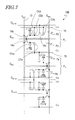
- FIG. 7 shows an equivalent circuit of three pixels (three pixels enclosed by the one-dot chain line in FIG. 6 ) in the liquid crystal display panel 10 E.
- FIG. 8 is a schematic plan view of a pixel electrode 11 A usable for a PSA mode liquid crystal display device in an embodiment according to the present invention.
- liquid crystal display devices in embodiments according to the present invention will be described with reference to the drawings.
- the present invention is not limited to the following embodiments provided as examples.
- FIG. 1( a ) is a schematic plan view of the liquid crystal display device 100
- FIG. 1( b ) is a schematic view showing electrical connections regarding pixels in a liquid crystal display panel 10 .
- the liquid crystal display device 100 includes the liquid crystal display panel 10 including a plurality of pixels P arrayed in a matrix of a plurality of rows by a plurality of columns, and a scanning line driving circuit (gate driver) 20 and a signal line driving circuit (source driver) 30 both for supplying driving signals to the liquid crystal display panel 10 .
- the plurality of pixels P in the liquid crystal display panel 10 form a plurality of color display pixels P CD , and each of the color display pixels P CD includes four pixels P.
- the four pixels P are a first pixel P 1 , a second pixel P 2 , a third pixel P 3 and a fourth pixel P 4 which are arrayed in two rows by two columns.
- the first pixel P 1 and the second pixel P 2 are adjacent to each other in a row direction
- the third pixel P 3 and the fourth pixel P 4 are adjacent to each other in the row direction.
- the first pixel P 1 and the third pixel P 3 are adjacent to each other in a column direction
- the second pixel P 2 and the fourth pixel P 4 are adjacent to each other in the column direction.
- the first pixel P 1 is a red (R) pixel
- the second pixel P 2 is a yellow (R) pixel
- the third pixel P 3 is a blue (B) pixel
- the fourth pixel P 4 is a green (G) pixel.
- FIG. 1( a ) shows one row and one column of the color display pixels and omits the other color display pixels. The same color display pixels as those shown in the figure are arrayed in a matrix.
- the colors of the four pixels P 1 through P 4 included in the color display pixel are not limited to the above. From the point of view of color reproducibility, it is preferable that at least R, G and B pixels are included.
- the other color is yellow (Y), cyan (C) or magenta (M), but may be white (W).
- each pixel is generally rectangular, that the first pixel P 1 and the second pixel P 2 arrayed in the row direction have an equal length in the column direction, that the third pixel P 3 and the fourth second pixel P 4 arrayed in the row direction have an equal length in the column direction, that the first pixel P 1 and the third pixel P 3 arrayed in the column direction have an equal length (width) in the row direction, and that the second pixel P 2 and the fourth pixel P 4 arrayed in the column direction have an equal length (width) in the row direction.
- the color display pixel P CD is generally square.
- FIG. 1( b ) is a plan view of an active matrix substrate (TFT substrate) 10 a included in the liquid crystal display panel 10 , but omits a liquid crystal layer and a counter substrate located to face the active matrix substrate 10 a with the liquid crystal layer being held therebetween.
- the counter substrate typically includes a counter electrode, a color filter layer, a light blocking layer (black matrix), and the like.
- the color filter layer may be provided in the active matrix substrate.
- the counter electrode may be provided in the active matrix substrate.
- FIG. 1( b ) shows an area of the active matrix substrate 10 a which corresponds to four pixels included in one color display pixel P CD .
- the active matrix substrate 10 a includes a pixel electrode 11 provided for each of the pixels P, a switching element (in this example, TFT) 14 connected to the pixel electrode 11 , a plurality of scanning lines (gate bus lines) 12 extending in the row direction, and a plurality of signal lines (source bus lines) 13 extending in the column direction.
- the scanning line driving circuit 20 shown in FIG. 1( a ) supplies a scanning signal to each of the plurality of scanning lines 12
- the signal line driving circuit 30 shown in FIG. 1( a ) supplies a positive or negative signal voltage to each of the plurality of signal lines 13 .
- a TFT type liquid crystal display device including the TFT 14 as a switching element will be described, but the switching element may be anything which operates in substantially the same manner as the TFT 14 .
- the plurality of signal lines 13 include a first signal line 13 a and a second signal line 13 b which are provided in correspondence with each column of pixels.
- the first signal line 13 a and the second signal line 13 b are supplied with signal voltages of opposite polarities from each other from the signal line driving circuit 30 in each vertical scanning period.
- the first signal line 13 a is supplied with a positive signal voltage
- the second signal line 13 b is supplied with a negative signal voltage.
- the left signal line is referred to as the “first signal line 13 a ” and the right signal line is referred to as the “second signal line 13 b ”.
- the polarities of the signal voltages supplied to the first signal line 13 a and the second signal line 13 b are independent in each column of pixels. Specifically, referring to FIG. 1( b ) , the polarity of the signal voltage supplied to a first signal line S a(n) located in correspondence with an n'th column of pixels, and the polarity of the signal voltage supplied to a first signal line S a(n+1) located in correspondence with the (n+1)th column of pixels, are independent from each other.
- the polarity of the signal voltage supplied to a second signal line S b(n) located in correspondence with the n'th column of pixels, and the polarity of the signal voltage supplied to a second signal line S b(n+1) located in correspondence with the (n+1)th column of pixels, are independent from each other.
- the polarity of the signal voltage supplied to the first signal line S a(n) and the polarity of the signal voltage supplied to the second signal line S b(n) are opposite to each other.
- the polarity of the signal voltage supplied to the first signal line S a(n+1) and the polarity of the signal voltage supplied to the second signal line S b(n+1) are opposite to each other.
- the TFT 14 of one of the first pixel P 1 and the third pixel P 3 is connected to the first signal line 13 a
- the TFT 14 of the other of the first pixel P 1 and the third pixel P 3 is connected to the second signal line 13 b
- the TFT 14 of one of the second pixel P 2 and the fourth pixel P 4 is connected to the first signal line 13 a
- the TFT 14 of the other of the second pixel P 2 and the fourth pixel P 4 is connected to the second signal line 13 b .
- the TFT 14 of the first pixel P 1 is connected to the first signal line 13 a
- the TFT 14 of the third pixel P 3 is connected to the second signal line 13 b
- the TFT 14 of the third pixel P 3 is connected to the second signal line 13 b
- the TFT 14 of the fourth pixel P 4 is connected to the first signal line 13 a .
- the TFTs may each be connected to the opposite signal line.
- the TFTs 14 of the four pixels P 1 through P 4 are all controlled to be ON/OFF by a common scanning signal.
- the TFTs 14 of the four pixels P 1 through P 4 are all connected to a common scanning line 12 .
- the scanning signal may be supplied from different scanning lines.
- one pixel electrode includes two sub pixel electrodes, specifically, a bright sub pixel exhibiting a luminance higher than that of the gray scale level to be displayed and a dark sub pixel exhibiting a luminance lower than that of the gray scale level to be displayed, two scanning lines are provided in correspondence with the two sub pixel electrodes and a common scanning signal is supplied to the scanning lines.
- the four pixels P 1 through P 4 included in one color display pixel P CD are driven by one scanning line G (m) , and four signal lines S a(n) , S b(n) , S a(n+1) and S b(n+1) .
- the time required for supplying a signal voltage to each pixel time period in which the TFT 14 is in an ON state; also referred to as the “write time” can be the same as in the conventional stripe-array structure. Accordingly, there is no obstacle against double speed or quadruple speed driving performed on the scanning and signal lines.
- the polarity of the voltage applied to the first pixel P 1 and the polarity of the voltage applied to the third pixel P 3 are opposite to each other, and the polarity of the voltage applied to the second pixel P 2 and the polarity of the voltage applied to the fourth pixel P 4 are opposite to each other. Therefore, among two among the four pixels P 1 through P 4 included in each color display pixel P CD , two pixels are supplied with a positive voltage, and the other two pixels are supplied with a negative voltage.
- the polarities of the signal voltages supplied to the first signal line 13 a and the second signal line 13 b are constant.
- AC driving is performed and therefore the polarities of the signal voltages supplied to the first signal line 13 a and the second signal line 13 b are inverted at intervals of a vertical scanning period.
- the signal line driving circuit 30 merely inverts the polarity of the signal voltage supplied to each signal line 13 at intervals of a vertical scanning period, regardless of the number of rows of pixels (i.e., the cycle of polarity inversion is twice the vertical scanning period).
- the load on the signal line driving circuit 30 of the liquid crystal display device 100 is smaller than the load on the signal line driving circuit in the liquid crystal display devices described in Patent Documents 1 and 2 or a conventionally common stripe array type liquid crystal display device.
- the polarity of the signal voltage supplied to each signal line 13 is inverted at intervals of a vertical scanning period.
- the polarity of the signal voltage supplied to each signal line 13 may be inverted at intervals of two or more vertical scanning periods. For example, when one, same image is written with the same polarity for two vertical scanning periods during driving at 240 Hz, there is an advantage that a sufficient time for charging the pixel can be obtained. As the cycle of polarity inversion is longer, the power consumption is smaller.
- the above-described advantage of the liquid crystal display device 100 is conspicuous when double speed or quadruple speed driving is performed, namely, when the vertical scanning period is 1/120 sec. or less. Even when the conventional 60 Hz driving is performed, there is an advantage that the power consumption can be reduced. Therefore, as described in Patent Documents 1 and 2, it is preferable that the liquid crystal display device is structured so as to prevent flicker.
- FIG. 2 through FIG. 5 a structure for preventing flicker will be described.
- FIG. 2 through FIG. 5 show the connections between the TFTs 14 of the four pixels P 1 through P 4 and the two signal lines 13 , and a polarity distribution of the signal voltages applied to the pixels, in liquid crystal display panels 10 A through 10 D usable as the liquid crystal display panel 10 of the liquid crystal display device 100 .
- the liquid crystal display panels 10 A through 10 D shown in FIG. 2 through FIG. 5 each have the structure of the liquid crystal display panel 10 described above with reference to FIG. 1 .
- the polarity of the signal voltage supplied to each signal line 13 is not changed during the vertical scanning period and is inverted at intervals of a vertical scanning period.
- FIG. 2 through FIG. 5 show the polarities of the signal voltages applied to the pixels in a certain vertical scanning period. At the next vertical scanning period, the polarities of the signal voltages applied to the pixels are all inverted.
- the signal lines S a(n) and S a(n+1) are of the same polarity (in this example, positive), and the signal lines S b(n) and S b(n+1) are of the same polarity (in this example, negative).
- the signal lines S a(n) and S b(n+1) are of the same polarity (in this example, positive), and the signal lines S b(n) and S a(n+1) are of the same polarity (in this example, negative).
- the signal line driving circuit for dot inversion driving of a conventional liquid crystal display device having a stripe array of R, G and B pixels can be used as it is.
- the TFT 14 of the first pixel P 1 is connected to the first signal line S a(n)
- the TFT 14 of the third pixel P 3 is connected to the second signal line S b(n)
- the TFT 14 of the second pixel P 2 is connected to the second signal line S b(n+1)
- the TFT 14 of the fourth pixel P 4 is connected to the first signal line S a(n+1) .
- the polarities of the signal voltages supplied to the four pixels P 1 through P 4 are opposite to each other, and the polarities of the signal voltages supplied to the third pixel P 3 and the fourth pixel P 4 are opposite to each other.
- the color display pixel P CD including the first pixel P 1 of the (m+1)th row and the n'th column will be described.
- the TFT 14 of the first pixel P 1 is connected to the second signal line S b(n)
- the TFT 14 of the third pixel P 3 is connected to the first signal line S a(n)
- the TFT 14 of the second pixel P 2 is connected to the first signal line S a(n+1)
- the TFT 14 of the fourth pixel P 4 is connected to the second signal line S b(n+1) .
- the connection relationship between the TFTs 14 of the four pixels P 1 through P 4 and the two signal lines 13 e.g., signal lines S a(n) and S b(n) , and signal lines S a(n+1) and S b(n+1) ) is opposite to that in the other of the two color display pixels.
- the polarities of the voltages applied to the pixels of a same color which are adjacent to each other in the column direction are opposite to each other.
- the first pixel P 1 of the m'th row and the n'th column is supplied with a positive voltage
- the first pixel P 1 of the (m+1)th row and the n'th column is supplied with a negative voltage.
- the polarities of the voltages applied to the pixels of a same color which are adjacent to each other in the column direction are opposite to each other.
- the color display pixel P CD including the first pixel P 1 of the m'th row and the (n+2)th column will be described.
- the TFT 14 of the first pixel P 1 is connected to the second signal line S b(n+2)
- the TFT 14 of the third pixel P 3 is connected to the first signal line S a(n+2)
- the TFT 14 of the second pixel P 2 is connected to the first signal line S a(n+3)
- the TFT 14 of the fourth pixel P 4 is connected to the second signal line S b(n+3) .
- the connection relationship between the TFTs 14 of the four pixels P 1 through P 4 and the two signal lines 13 e.g., signal lines S a(n) and S b(n) , and signal lines S a(n+2) and S b(n+2) ) is opposite to that in the other of the two color display pixels.
- the polarities of the voltages applied to the pixels of a same color which are adjacent to each other in the row direction are opposite to each other.
- the first pixel P 1 of the m'th row and the n'th column is supplied with a positive voltage
- the first pixel P 1 of the m'th row and the (n+2)th column is supplied with a negative voltage.
- the polarities of the voltages applied to the pixels of a same color which are adjacent to each other in the row direction are opposite to each other.
- the polarity of the voltage applied to the first pixel P 1 (hatched) in one color display pixel is opposite to that in a color display pixel adjacent to the one color display pixel in the column direction, and is opposite to that in a color display pixel adjacent to the one color display pixel in the row direction.
- the second through fourth pixels also have this relationship. Accordingly, the liquid crystal display panel 10 A can prevent flicker as the liquid crystal display devices described in Patent Documents 1 and 2.
- FIG. 3 will be referred to.
- the TFT 14 of the first pixel P 1 is connected to the first signal line S a(n)
- the TFT 14 of the third pixel P 3 is connected to the second signal line S b(n)
- the TFT 14 of the second pixel P 2 is connected to the first signal line S a(n+1)
- the TFT 14 of the fourth pixel P 4 is connected to the second signal line S b(n+1) .
- connection relationship between the TFTs 14 and the two signal lines S a(n+1) and S b(n+1) regarding the second pixel P 2 and the fourth pixel P 4 is opposite to that of the liquid crystal display panel 10 A shown in FIG. 2 . Accordingly, regarding the polarities of the signal voltages supplied to the four pixels P 1 through P 4 , the polarities of the signal voltages supplied to the first pixel P 1 and the second pixel P 2 are the same as each other, and the polarities of the signal voltages supplied to the third pixel P 3 and the fourth pixel P 4 are the same as each other.
- the color display pixel P CD including the first pixel P 1 of the (m+1)th row and the n'th column will be described.
- the TFT 14 of the first pixel P 1 is connected to the second signal line S b(n)
- the TFT 14 of the third pixel P 3 is connected to the first signal line S a(n)
- the TFT 14 of the second pixel P 2 is connected to the second signal line S b(n+1)
- the TFT 14 of the fourth pixel P 4 is connected to the first signal line S a(n+1) .
- the connection relationship between the TFTs 14 of the four pixels P 1 through P 4 and the two signal lines 13 e.g., signal lines S a(n) and S b(n) , and signal lines S a(n+1) and S b(n+1) ) is opposite to that in the other of the two color display pixels.
- the polarities of the voltages applied to the pixels of a same color which are adjacent to each other in the column direction are opposite to each other.
- the first pixel P 1 of the m'th row and the n'th column is supplied with a positive voltage
- the first pixel P 1 of the (m+1)th row and the n'th column is supplied with a negative voltage.
- the polarities of the voltages applied to the pixels of a same color which are adjacent to each other in the column direction are opposite to each other.
- the color display pixel P CD including the first pixel P 1 of the m'th row and the (n+2)th column will be described.
- the TFT 14 of the first pixel P 1 is connected to the second signal line S b(n+2)
- the TFT 14 of the third pixel P 3 is connected to the first signal line S a(n+2)
- the TFT 14 of the second pixel P 2 is connected to the second signal line S b(n+3)
- the TFT 14 of the fourth pixel P 4 is connected to the first signal line S a(n+3) .
- the connection relationship between the TFTs 14 of the four pixels P 1 through P 4 and the two signal lines 13 e.g., signal lines S a(n) and S b(n) , and signal lines S a(n+2) and S b(n+2) ) is opposite to that in the other of the two color display pixels.
- the polarities of the voltages applied to the pixels of a same color which are adjacent to each other in the row direction are opposite to each other.
- the first pixel P 1 of the m'th row and the n'th column is supplied with a positive voltage
- the first pixel P 1 of the m'th row and the (n+2)th column is supplied with a negative voltage.
- the polarities of the voltages applied to the pixels of a same color which are adjacent to each other in the row direction are opposite to each other.
- the polarity of the voltage applied to the first pixel P 1 (hatched) in one color display pixel is opposite to that in a color display pixel adjacent to the one color display pixel in the column direction, and is opposite to that in a color display pixel adjacent to the one color display pixel in the row direction.
- the second through fourth pixels also have this relationship. Accordingly, the liquid crystal display panel 10 B can also prevent flicker as the liquid crystal display devices described in Patent Documents 1 and 2.
- FIG. 4 will be referred to.
- the TFT 14 of the first pixel P 1 is connected to the first signal line S a(n)
- the TFT 14 of the third pixel P 3 is connected to the second signal line S b(n)
- the TFT 14 of the second pixel P 2 is connected to the first signal line S a(n+1)
- the TFT 14 of the fourth pixel P 4 is connected to the second signal line S b(n+1) .
- connection relationship between the TFTs 14 of the four pixels P 1 through P 4 and the two signal lines 13 in the liquid crystal display panel 10 C is the same as that of the liquid crystal display panel 10 B shown in FIG. 3 .
- the difference between the liquid crystal display panel 10 C and the liquid crystal display panel 10 B is in the polarities of the voltage signals supplied to the signal lines 13 .
- the signal lines S a(n) and S a(n+1) are of the same polarity (in this example, positive), and the signal lines S b(n) and S b(n+1) are of the same polarity (in this example, negative).
- the signal lines S a(n) and S b(n+1) are of the same polarity (in this example, positive), and the signal lines S b(n) and S a(n+1) are of the same polarity (in this example, negative).
- the polarity distribution of FIG. 3 matches the polarity distribution of FIG. 4 .
- the polarities of the signal voltages supplied to the four pixels P 1 through P 4 the polarities of the signal voltages supplied to the first pixel P 1 and the second pixel P 2 are opposite to each other, and the polarities of the signal voltages supplied to the third pixel P 3 and the fourth pixel P 4 are opposite to each other.
- the polarity of the voltage applied to the first pixel P 1 (hatched) in one color display pixel is opposite to that in a color display pixel adjacent to the one color display pixel in the column direction, and is opposite to that in a color display pixel adjacent to the one color display pixel in the row direction.
- the second through fourth pixels also have this relationship. Accordingly, the liquid crystal display panel 10 C can also prevent flicker as the liquid crystal display devices described in Patent Documents 1 and 2.
- FIG. 5 will be referred to.
- the TFT 14 of the first pixel P 1 is connected to the first signal line S a(n)
- the TFT 14 of the third pixel P 3 is connected to the second signal line S b(n)
- the TFT 14 of the second pixel P 2 is connected to the second signal line S b(n+1)
- the TFT 14 of the fourth pixel P 4 is connected to the first signal line S a(n+1) .
- connection relationship between the TFTs 14 of the four pixels P 1 through P 4 and the two signal lines 13 in the liquid crystal display panel 10 D is the same as that of the liquid crystal display panel 10 A shown in FIG. 2 .
- the difference between the liquid crystal display panel 10 D and the liquid crystal display panel 10 A is in the polarities of the voltage signals supplied to the signal lines 13 .
- the signal lines S a(n) and S a(n+1) are of the same polarity (in this example, positive), and the signal lines S b(n) and S b(n+1) are of the same polarity (in this example, negative).
- the signal lines S a(n) and S b(n+1) are of the same polarity (in this example, positive), and the signal lines S b(n) and S a(n+1) are of the same polarity (in this example, negative).
- the polarity distribution of FIG. 5 matches the polarity distribution of FIG. 2 .
- the polarities of the signal voltages supplied to the four pixels P 1 through P 4 are the same as each other, and the polarities of the signal voltages supplied to the third pixel P 3 and the fourth pixel P 4 are the same as each other.
- the polarity of the voltage applied to the first pixel P 1 (hatched) in one color display pixel is opposite to that in a color display pixel adjacent to the one color display pixel in the column direction, and is opposite to that in a color display pixel adjacent to the one color display pixel in the row direction.
- the second through fourth pixels also have this relationship. Accordingly, the liquid crystal display panel 10 D can also prevent flicker as the liquid crystal display devices described in Patent Documents 1 and 2.
- the “multi-pixel structure” is a structure in which for displaying a certain intermediate gray scale level, each pixel includes a bright sub pixel exhibiting a luminance higher than that of the gray scale level to be displayed and a dark sub pixel exhibiting a luminance lower than that of the gray scale level to be displayed.
- the viewing angle dependence of the ⁇ characteristic can be alleviated.
- a structure described in Japanese Laid-Open Patent Publication No. 2006-133577 for example, can be adopted.
- the disclosure of Japanese Laid-Open Patent Publication No. 2006-133577 is entirely incorporated herein by reference.
- FIG. 6 shows the connection relationship between the TFTs of the pixels and the signal lines, and also shows the timing at which a gate signal as a scanning signal is turned ON.
- FIG. 7 shows an equivalent circuit of three pixels enclosed by the one-dot chain line in FIG. 6 .
- the liquid crystal display panel 10 E shown in FIG. 6 is obtained as a result of applying the multi-pixel structure to the liquid crystal display panel 10 A shown in FIG. 2 .
- the four pixels P 1 through P 4 each include a sub pixel Pa and a sub pixel Pb.
- the sub pixel Pa is a bright sub pixel
- the sub pixel Pb is a dark sub pixel.
- the bright sub pixel Pa and the dark sub pixel Pb are obtained as a result of dividing each pixel into two in the column direction.
- the bright sub pixel Pa and the dark sub pixel Pb are shown as having an approximately equal area size.
- the area size ratio of the bright sub pixel Pa and the dark sub pixel Pb is not limited to this, and may be changed when necessary.
- the bright pixels Pa in the four pixels P 1 through P 4 included in the color display pixel P CD are located at a center of the color display pixel P CD in the column direction.
- the lower sub pixels in the first pixel P 1 and the second pixel P 2 and the upper sub pixels in the third pixel P 3 and the fourth pixel P 4 are the bright sub pixels Pa.
- colors may blur.
- a white square or rectangle having edges parallel to the rows of pixels is displayed, at the upper edge of the rectangle, the bright sub pixels in the first and second pixels of the row of pixels corresponding to the edge are conspicuous. Namely, the bright sub pixels in the pixels of two colors are conspicuous. As a result, the color of the upper edge of the white rectangle appears to blur.
- the bright sub pixels Pa of the four pixels P 1 through P 4 included in the color display pixel P CD are located at a center of the color display pixel P CD in the column direction, the bright sub pixels Pa of the four pixels are close to each other. Therefore, color blur can be prevented.
- the four pixels P 1 through P 4 each include the bright sub pixel Pa and the dark sub pixel Pb.
- the bright sub pixel Pa is connected to a TFT 14 a
- the dark sub pixel Pb is connected to a TFT 14 b .
- Gates of the TFTs 14 a and 14 b are connected to a common scanning line 12
- sources of the TFTs 14 a and 14 b are connected to a common signal line 13 .
- the sub pixels Pa and Pb each include a sub pixel electrode corresponding to the pixel electrode 11 shown in FIG. 1( b ) .
- the sub pixel electrodes of the sub pixels Pa and Pb are connected to drains of the corresponding TFTs 14 a and 14 b and are connected to the common signal line (source sub line) 13 via the TFTs 14 a and 14 b.
- the TFTs 14 of the first pixel P 1 , the second pixel P 2 , the third pixel P 3 and the fourth pixel P 4 namely, four TFTs 14 in total are connected to the common scanning line (gate sub line) 12 .
- the TFTs of the bright sub pixel and the dark sub pixel of the first pixel P 1 and the bright sub pixel and the dark sub pixel of the second pixel P 2 namely, four TFTs 14 a and 14 b in total are connected to a common scanning line (gate sub line) 12 (e.g., the upper scanning line G (m) in FIG. 6 ).
- the TFTs of the bright sub pixel and the dark sub pixel of the third pixel P 3 and the bright sub pixel and the dark sub pixel of the fourth pixel P 4 namely, four TFTs 14 a and 14 b in total are connected to another common scanning line 12 (e.g., the lower scanning line G (m) in FIG. 6 ). As shown in FIG. 6 , these two scanning lines 12 are supplied with a common gate signal. Referring to FIG. 6 , during the period in which the gate signal is HIGH, the TFTs 14 a and 14 b are in an ON state, and signal voltages are supplied from the corresponding signal lines 13 .
- the sub pixels of the four pixels P 1 through P 4 (eight sub pixels in total) in the liquid crystal display panel 10 E are each supplied with a corresponding signal voltage when the corresponding TFTs 14 a and 14 b are turned ON (like the four pixels P 1 through P 4 in the liquid crystal display panel 10 A).
- the gates of the TFTs 14 a and 14 b are controlled to be ON/OFF by a common gate signal.
- the four pixels P 1 through P 4 in the liquid crystal display panel 10 E each further include a third TFT 14 c .
- the third TFT 14 c switches the electrical connection between a capacitance CSb of the dark sub pixel Pb and a buffer capacitance CSc connected parallel thereto.
- a gate of the TFT 14 c is connected to the next-stage scanning line (e.g., G (m+1) ), and is put into an ON state at the same timing as the TFTs 14 a and 14 b of the next-stage color display pixel, namely, the color display pixel which is adjacent to the color display pixel of interest in the column direction.
- the third TFT 14 c By putting the third TFT 14 c into an ON state, the sub pixel Pb becomes a dark sub pixel.
- a gate signal of the scanning line G (m) becomes HIGH
- the TFTs 14 a and 14 b are put into an ON state, and a prescribed signal (herein, V (k) ) is supplied from the signal line S a(n) to the sub pixels Pa and Pb.
- V (k) a prescribed signal
- a liquid crystal capacitance Clca and a storage capacitance CSa of the sub pixel Pa (these capacitances are also referred to as the “sub pixel capacitance C Pa ”
- a liquid crystal capacitance Clcb and a storage capacitance CSb of the sub pixel Pb are charged.
- One of the pixel electrodes forming each of the liquid crystal capacitances Clca and Clcb is the sub pixel electrode of the corresponding sub pixel, and the other electrode is the counter electrode.
- the counter electrode is supplied with a common voltage (counter voltage) COM.
- One of the electrodes forming each of the storage capacitances CSa and CSb is a storage capacitance electrode and is connected to a drain electrode of the TFT 14 a or 14 b .
- the storage capacitance electrode is supplied with the same voltage as that of the sub pixel electrode of the corresponding sub pixel.
- the other electrode forming each of the storage capacitances CSa and CSb is connected to a storage capacitance line (Cs) 15 and is supplied with a storage capacitance voltage.
- a gate signal of the scanning line G (m+1) is LOW, and thus the TFT 14 c is in an OFF state.
- the buffer capacitance CSc the signal voltage written in the immediately previous vertical scanning period (herein, V (k ⁇ 1) ) is retained.
- the liquid crystal display panel 10 E is driven by frame inversion driving. Therefore, the polarity of the voltage which is written in the current vertical scanning period is opposite to the polarity of the voltage written in the immediately previous vertical scanning period.
- the TFT 14 c is put into an ON state.
- the sub pixel capacitance C Pb and the buffer capacitance CSc are connected parallel to each other. Accordingly, the charges stored in the sub pixel capacitance C Pb and the charges stored in the buffer capacitance CSc are re-distributed such that voltage V (k) retained by the sub pixel capacitance C Pb and voltage V (k ⁇ 1) retained by the buffer capacitance CSc are equal to each other.
- V (k ⁇ 1) has a polarity opposite to the polarity of the V (k) .
- the overall charge amount stored in the sub pixel capacitance C Pb and the buffer capacitance CSc is reduced, and the voltage of the sub pixel capacitance C Pb becomes lower than voltage V (k) (the absolute value of the voltage of the sub pixel capacitance C Pb becomes smaller than that of V (k) ).
- the luminance of the sub pixel Pb becomes lower than the luminance of the sub pixel Pa in which voltage V (k) is retained.
- the above-described operation is usable to make the sub pixel Pb a dark sub pixel.
- the polarity is inverted to write a positive signal voltage.
- the luminance of the sub pixel Pb becomes lower than the luminance of the sub pixel Pa.
- the average luminance of the sub pixel Pb is lower than the luminance of the sub pixel Pa. Accordingly, even when the polarity of the signal voltage supplied to each signal line is inverted at intervals of two vertical scanning periods, the effect of the multi-pixel structure can be provided.
- the multi-pixel structure described in Japanese Laid-Open Patent Publication No. 2006-133577 is preferably usable for a vertical alignment type liquid crystal display device in which a plurality of liquid crystal domains are formed in one pixel and which provides display in a normally black mode.
- the plurality of liquid crystal domains include four liquid crystal domains, the directors of which have azimuth angles of 45°, 135°, 225° and 315° (where the rightward direction, i.e., the 3 o'clock direction of a clock face is 0°, and the counterclockwise direction is the positive direction) at least when a voltage is applied to the liquid crystal layer.
- FIG. 10 Another multi-pixel structure usable for a liquid crystal display device according to the present invention is disclosed in Japanese Laid-Open Patent Publication No. 2004-62146 (U.S. Pat. No. 6,958,791) filed by the present applicant.
- a storage capacitance is provided for each of a plurality of sub pixels included in one pixel, and a storage capacitance counter electrode forming the storage capacitance (connected to the CS bus line) is made electrically independent for each sub pixel.
- the voltages supplied to the storage capacitance counter electrodes (referred to as the “storage capacitance counter capacitances”) are made different.
- Japanese Laid-Open Patent Publication No. 2006-133577 describes a liquid crystal display device of the so-called MVA mode.
- MVA mode liquid crystal display device linear slits formed in electrodes and linear dielectric projections (ribs) formed on the electrodes on the liquid crystal layer side are located, on the pair of substrates facing each other while having a liquid crystal layer therebetween, to be parallel to, and alternate to, each other when seen in a direction normal to the substrates.
- the azimuth directions of the directors of the liquid crystal domains formed at the time of voltage application are regulated.
- the azimuth direction of each liquid crystal domain is perpendicular to the azimuth direction in which the linear slits or dielectric projections (collectively referred to as the “linear structures”) extend.
- PSA technology As a vertical alignment type liquid crystal display device having a response characteristic higher than that of the MVA mode liquid crystal display device, a PSA mode liquid crystal display device is known.
- the polymer sustained alignment technology (hereinafter, referred to as the “PSA technology”) is disclosed in, for example, Japanese Laid-Open Patent Publications Nos. 2002-357830, 2003-177418 and 2006-78968, and K. Hanaoka et al., “A New MVA-LCD by Polymer Sustained Alignment Technology”, SID 04 DIGEST, pp. 1200-1203 (2004). The disclosures of these four documents are entirely incorporated herein by reference.
- the pretilt direction of the liquid crystal molecules is controlled as follows.
- a small amount of polymerizable compound e.g., a photopolymerizable monomer or oligomer
- the polymerizable compound is irradiated with active energy rays (e.g., ultraviolet rays) in the state where a prescribed voltage is applied to the liquid crystal layer.
- active energy rays e.g., ultraviolet rays
- the pretilt direction of the liquid crystal molecules is controlled by the polymer which is thus generated.
- the alignment state of the liquid crystal molecules realized when the polymer is generated is maintained (stored) even after the voltage is removed (in the absence of the voltage).
- the layer formed of the polymer will be referred to as an “alignment sustaining layer”.
- the alignment sustaining layer is formed on surfaces of alignment films (on the liquid crystal layer side).
- the alignment sustaining layer does not need to be in the form of a film covering the surfaces of the alignment films, and may be in the form of particles of the polymer discretely provided.
- the PSA technology has an advantage of adjusting the pretilt azimuth angle and the pretilt angle of the liquid crystal molecules by controlling the electric field or the like formed in the liquid crystal layer.
- an alignment sustaining layer expresses an alignment regulating force on substantially the entire plane thereof contacting the liquid crystal layer, a higher response characteristic than that of the MVA mode liquid crystal display device is provided.
- the present invention is preferably applicable to a PSA mode liquid crystal display device.
- a PSA mode liquid crystal display device in an embodiment according to the present invention is obtained by, for example, using a pixel electrode 11 A shown in FIG. 8 as the pixel electrode 11 of the liquid crystal display panel 10 and applying the above-described PSA technology.
- the pixel electrode 11 A includes cross-shaped trunk portions 11 t 1 and 11 t 2 located to overlap polarizing axes of a pair of polarizing plates and a plurality of branch portions 11 b 1 , 11 b 2 , 11 b 3 and 11 b 4 extending in a direction of about 45° with respect to the cross-shaped trunk portions 11 t 1 and 11 t 2 .
- the trunk portions include the trunk portion 11 t 1 extending in the row direction (horizontal direction) and the trunk portion 11 t 2 extending in the column direction (vertical direction).
- the plurality of branch portions include a first group (branch portions 11 b 1 ) extending at an azimuth angle of 45° from the trunk portion, a second group (branch portions 11 b 2 ) extending at an azimuth angle of 135° from the trunk portion, a third group (branch portions 11 b 3 ) extending at an azimuth angle of 225° from the trunk portion, and a fourth group (branch portions 11 b 4 ) extending at an azimuth angle of 315° from the trunk portion.
- the liquid crystal molecules in the liquid crystal layer of the vertical alignment type are tilted in azimuth directions in which the corresponding branch portions extend because of oblique electric fields from the trunk portions and the branch portions.
- a reason for this is that an oblique electric field from the branch portions extending parallel to each other acts to tilt the liquid crystal molecules in an azimuth direction perpendicular to the direction in which the branch portions extend, and an oblique electric field from the trunk portions act to tilt the liquid crystal molecules in directions in which the corresponding branch portions extend.
- the present invention is widely applicable to liquid crystal display devices of, for example, an RTN (also referred to as “VAIN”) mode, an IPS mode and an FSS mode in addition to the liquid crystal display devices in the above embodiments.
- RTN also referred to as “VAIN”
- IPS IPS
- FSS FSS mode
- the row direction is set as the horizontal direction of the display plane and the column direction is set as the vertical direction of the display plane. These directions may be opposite. Namely, the gate bus lines may be located to extend in the vertical direction and the source bus lines may be located to extend in the horizontal direction. In other words, the row direction and the column direction in the above description may be exchanged.
- the present invention is widely applicable to liquid crystal display devices for HDTV and other applications.
Applications Claiming Priority (3)
| Application Number | Priority Date | Filing Date | Title |
|---|---|---|---|
| JP2010-019258 | 2010-01-29 | ||
| JP2010019258 | 2010-01-29 | ||
| PCT/JP2011/051586 WO2011093374A1 (ja) | 2010-01-29 | 2011-01-27 | 液晶表示装置 |
Publications (2)
| Publication Number | Publication Date |
|---|---|
| US20120320026A1 US20120320026A1 (en) | 2012-12-20 |
| US9818348B2 true US9818348B2 (en) | 2017-11-14 |
Family
ID=44319357
Family Applications (1)
| Application Number | Title | Priority Date | Filing Date |
|---|---|---|---|
| US13/575,691 Active 2033-08-31 US9818348B2 (en) | 2010-01-29 | 2011-01-27 | Liquid crystal display device |
Country Status (5)
| Country | Link |
|---|---|
| US (1) | US9818348B2 (zh) |
| EP (1) | EP2530513A4 (zh) |
| JP (1) | JP5540020B2 (zh) |
| CN (1) | CN102725676B (zh) |
| WO (1) | WO2011093374A1 (zh) |
Cited By (1)
| Publication number | Priority date | Publication date | Assignee | Title |
|---|---|---|---|---|
| US10891909B2 (en) | 2017-07-11 | 2021-01-12 | Mitsubishi Electric Corporation | Display device and method for driving same |
Families Citing this family (15)
| Publication number | Priority date | Publication date | Assignee | Title |
|---|---|---|---|---|
| CN102750919A (zh) * | 2012-06-26 | 2012-10-24 | 北京京东方光电科技有限公司 | 一种显示面板及其驱动方法、显示装置 |
| US9489902B2 (en) * | 2012-09-13 | 2016-11-08 | Sharp Kabushiki Kaisha | Liquid crystal display device |
| CN104395952B (zh) * | 2012-12-07 | 2017-08-15 | 堺显示器制品株式会社 | 液晶显示装置及该液晶显示装置的驱动方法 |
| US9697787B2 (en) * | 2013-09-09 | 2017-07-04 | Samsung Display Co., Ltd. | Display device |
| KR102114818B1 (ko) * | 2013-09-09 | 2020-05-26 | 삼성디스플레이 주식회사 | 표시 장치 |
| CN103792746A (zh) * | 2014-01-27 | 2014-05-14 | 北京京东方光电科技有限公司 | 一种阵列基板、其制备方法及显示装置 |
| JP2015165272A (ja) * | 2014-03-03 | 2015-09-17 | 株式会社ジャパンディスプレイ | 表示装置及び反射型液晶表示装置 |
| KR20160025146A (ko) | 2014-08-26 | 2016-03-08 | 삼성디스플레이 주식회사 | 표시 장치 |
| JP2016184097A (ja) * | 2015-03-26 | 2016-10-20 | 株式会社ジャパンディスプレイ | 表示装置 |
| CN107924662A (zh) * | 2015-08-27 | 2018-04-17 | 堺显示器制品株式会社 | 液晶显示装置 |
| CN105954951B (zh) * | 2016-07-08 | 2019-03-22 | 深圳市华星光电技术有限公司 | 一种液晶显示面板 |
| JP2019049590A (ja) | 2017-09-08 | 2019-03-28 | シャープ株式会社 | アクティブマトリクス基板およびデマルチプレクサ回路 |
| CN107871485B (zh) * | 2017-12-19 | 2019-08-27 | 惠科股份有限公司 | 一种显示面板、显示装置及驱动方法 |
| JP2022178523A (ja) | 2021-05-20 | 2022-12-02 | シャープディスプレイテクノロジー株式会社 | アクティブマトリクス基板および液晶表示装置 |
| CN113325644A (zh) * | 2021-05-31 | 2021-08-31 | Tcl华星光电技术有限公司 | 显示面板和电子设备 |
Citations (17)
| Publication number | Priority date | Publication date | Assignee | Title |
|---|---|---|---|---|
| JP2001033757A (ja) | 1999-07-21 | 2001-02-09 | Nec Corp | アクティブマトリクス型液晶表示装置 |
| US20010026331A1 (en) * | 2000-03-23 | 2001-10-04 | Masuyuki Oota | Liquid crystal display device |
| JP2002357830A (ja) | 2001-03-30 | 2002-12-13 | Fujitsu Ltd | 液晶表示装置 |
| US20030090450A1 (en) * | 2001-11-14 | 2003-05-15 | Kabushiki Kaisha Toshiba | Liquid crystal display device having a circuit for controlling polarity of video signal for each pixel |
| JP2003177418A (ja) | 2001-10-02 | 2003-06-27 | Fujitsu Display Technologies Corp | 液晶表示装置用基板及びそれを用いた液晶表示装置 |
| US20030146893A1 (en) | 2002-01-30 | 2003-08-07 | Daiichi Sawabe | Liquid crystal display device |
| JP2004062146A (ja) | 2002-06-06 | 2004-02-26 | Sharp Corp | 液晶表示装置 |
| US6952252B2 (en) | 2001-10-02 | 2005-10-04 | Fujitsu Display Technologies Corporation | Substrate for liquid crystal display and liquid crystal display utilizing the same |
| US20060055858A1 (en) | 2004-09-13 | 2006-03-16 | Fujitsu Display Technologies Corporation | Liquid crystal display device and manufacturing method therefor |
| JP2006133577A (ja) | 2004-11-08 | 2006-05-25 | Sharp Corp | 液晶表示装置用基板及びそれを備えた液晶表示装置及びその駆動方法 |
| US20080074601A1 (en) | 2006-09-26 | 2008-03-27 | Samsung Electronics Co., Ltd. | Liquid crystal display |
| JP2008076416A (ja) | 2004-12-27 | 2008-04-03 | Sharp Corp | 表示パネルの駆動装置、表示パネル及びそれを備えた表示装置並びに表示パネルの駆動方法 |
| CN101424821A (zh) | 2008-12-09 | 2009-05-06 | 友达光电股份有限公司 | 像素结构 |
| WO2009084331A1 (ja) | 2007-12-27 | 2009-07-09 | Sharp Kabushiki Kaisha | 液晶表示装置、液晶表示装置の駆動方法、テレビジョン受像機 |
| US20090189881A1 (en) * | 2008-01-25 | 2009-07-30 | Hitachi Displays, Ltd. | Display device |
| US20090303219A1 (en) * | 2008-06-09 | 2009-12-10 | Semiconductor Energy Laboratory Co., Ltd. | Display device, liquid crystal display device and electronic device including the same |
| US20100020257A1 (en) * | 2008-07-23 | 2010-01-28 | Samsung Electronics Co., Ltd. | Liquid crystal display device and manufacturing method thereof |
Family Cites Families (2)
| Publication number | Priority date | Publication date | Assignee | Title |
|---|---|---|---|---|
| US8648889B2 (en) * | 2005-11-30 | 2014-02-11 | Sharp Kabushiki Kaisha | Display device and method for driving display member |
| WO2008047725A1 (fr) * | 2006-10-13 | 2008-04-24 | Sharp Kabushiki Kaisha | Dispositif d'affichage et dispositif de conversion de signaux |
-
2011
- 2011-01-27 CN CN201180007473.9A patent/CN102725676B/zh not_active Expired - Fee Related
- 2011-01-27 EP EP11737085.8A patent/EP2530513A4/en not_active Withdrawn
- 2011-01-27 US US13/575,691 patent/US9818348B2/en active Active
- 2011-01-27 WO PCT/JP2011/051586 patent/WO2011093374A1/ja active Application Filing
- 2011-01-27 JP JP2011551896A patent/JP5540020B2/ja not_active Expired - Fee Related
Patent Citations (26)
| Publication number | Priority date | Publication date | Assignee | Title |
|---|---|---|---|---|
| JP2001033757A (ja) | 1999-07-21 | 2001-02-09 | Nec Corp | アクティブマトリクス型液晶表示装置 |
| US6552706B1 (en) * | 1999-07-21 | 2003-04-22 | Nec Corporation | Active matrix type liquid crystal display apparatus |
| US20010026331A1 (en) * | 2000-03-23 | 2001-10-04 | Masuyuki Oota | Liquid crystal display device |
| JP2002357830A (ja) | 2001-03-30 | 2002-12-13 | Fujitsu Ltd | 液晶表示装置 |
| US6977704B2 (en) | 2001-03-30 | 2005-12-20 | Fujitsu Display Technologies Corporation | Liquid crystal display |
| JP2003177418A (ja) | 2001-10-02 | 2003-06-27 | Fujitsu Display Technologies Corp | 液晶表示装置用基板及びそれを用いた液晶表示装置 |
| US6952252B2 (en) | 2001-10-02 | 2005-10-04 | Fujitsu Display Technologies Corporation | Substrate for liquid crystal display and liquid crystal display utilizing the same |
| US20030090450A1 (en) * | 2001-11-14 | 2003-05-15 | Kabushiki Kaisha Toshiba | Liquid crystal display device having a circuit for controlling polarity of video signal for each pixel |
| US20030146893A1 (en) | 2002-01-30 | 2003-08-07 | Daiichi Sawabe | Liquid crystal display device |
| JP2004062146A (ja) | 2002-06-06 | 2004-02-26 | Sharp Corp | 液晶表示装置 |
| US6958791B2 (en) | 2002-06-06 | 2005-10-25 | Sharp Kabushiki Kaisha | Liquid crystal display |
| JP2006078968A (ja) | 2004-09-13 | 2006-03-23 | Sharp Corp | 液晶表示装置およびその製造方法 |
| US20060055858A1 (en) | 2004-09-13 | 2006-03-16 | Fujitsu Display Technologies Corporation | Liquid crystal display device and manufacturing method therefor |
| JP2006133577A (ja) | 2004-11-08 | 2006-05-25 | Sharp Corp | 液晶表示装置用基板及びそれを備えた液晶表示装置及びその駆動方法 |
| US20060215066A1 (en) | 2004-11-08 | 2006-09-28 | Sharp Kabushiki Kaisha | Substrate for liquid crystal display, liquid crystal display having the substrate, and method of driving the display |
| US20090225103A1 (en) | 2004-12-27 | 2009-09-10 | Sharp Kabushiki Kaisha | Driving device for display panel, display panel, display device including the driving device, and method for driving display panel |
| JP2008076416A (ja) | 2004-12-27 | 2008-04-03 | Sharp Corp | 表示パネルの駆動装置、表示パネル及びそれを備えた表示装置並びに表示パネルの駆動方法 |
| US7920114B2 (en) * | 2004-12-27 | 2011-04-05 | Sharp Kabushiki Kaisha | Driving device for display panel, display panel, display device including the driving device, and method for driving display panel |
| US20080074601A1 (en) | 2006-09-26 | 2008-03-27 | Samsung Electronics Co., Ltd. | Liquid crystal display |
| WO2009084331A1 (ja) | 2007-12-27 | 2009-07-09 | Sharp Kabushiki Kaisha | 液晶表示装置、液晶表示装置の駆動方法、テレビジョン受像機 |
| US20100253668A1 (en) | 2007-12-27 | 2010-10-07 | Toshinori Sugihara | Liquid crystal display, liquid crystal display driving method, and television receiver |
| US20090189881A1 (en) * | 2008-01-25 | 2009-07-30 | Hitachi Displays, Ltd. | Display device |
| JP2009175468A (ja) | 2008-01-25 | 2009-08-06 | Hitachi Displays Ltd | 表示装置 |
| US20090303219A1 (en) * | 2008-06-09 | 2009-12-10 | Semiconductor Energy Laboratory Co., Ltd. | Display device, liquid crystal display device and electronic device including the same |
| US20100020257A1 (en) * | 2008-07-23 | 2010-01-28 | Samsung Electronics Co., Ltd. | Liquid crystal display device and manufacturing method thereof |
| CN101424821A (zh) | 2008-12-09 | 2009-05-06 | 友达光电股份有限公司 | 像素结构 |
Non-Patent Citations (3)
| Title |
|---|
| English translation of Official Communication issued in corresponding International Application PCT/JP2011/051586, dated on Sep. 27, 2012. |
| Hanaoka et al., "40.1: A New MVA-LCD by Polymer Sustained Alignment Technology," SID 04 Digest, 2004, pp. 1200-1203. |
| Official Communication issued in International Patent Application No. PCT/JP2011/051586, dated on Apr. 26, 2011. |
Cited By (1)
| Publication number | Priority date | Publication date | Assignee | Title |
|---|---|---|---|---|
| US10891909B2 (en) | 2017-07-11 | 2021-01-12 | Mitsubishi Electric Corporation | Display device and method for driving same |
Also Published As
| Publication number | Publication date |
|---|---|
| JPWO2011093374A1 (ja) | 2013-06-06 |
| EP2530513A1 (en) | 2012-12-05 |
| WO2011093374A1 (ja) | 2011-08-04 |
| CN102725676A (zh) | 2012-10-10 |
| US20120320026A1 (en) | 2012-12-20 |
| JP5540020B2 (ja) | 2014-07-02 |
| CN102725676B (zh) | 2015-10-07 |
| EP2530513A4 (en) | 2013-08-14 |
Similar Documents
| Publication | Publication Date | Title |
|---|---|---|
| US9818348B2 (en) | Liquid crystal display device | |
| US7916108B2 (en) | Liquid crystal display panel with color washout improvement and applications of same | |
| US9251746B2 (en) | Liquid crystal display apparatus | |
| US8885131B2 (en) | Liquid crystal display device | |
| US8248336B2 (en) | Liquid crystal display device and operating method thereof | |
| TWI393094B (zh) | 液晶顯示裝置及其驅動方法 | |
| US9715133B2 (en) | Liquid crystal display and driving method thereof | |
| US7830346B2 (en) | Liquid crystal display panel with color washout improvement by scanning line coupling and applications of same | |
| WO2011093243A1 (ja) | 液晶表示装置 | |
| US20110310075A1 (en) | Liquid crystal display and driving method thereof | |
| US8319918B2 (en) | Multi-domain display using fringe fields | |
| KR20090001226A (ko) | 표시 장치 및 그의 구동 방법 | |
| EP2549324A1 (en) | Liquid crystal display device | |
| KR101074381B1 (ko) | 횡전계방식 액정표시장치 | |
| US20120154716A1 (en) | Liquid crystal display | |
| US8902373B2 (en) | Liquid crystal display device | |
| US8605239B2 (en) | Display unit with interleaved pixels | |
| CN109164611B (zh) | 阵列基板及其驱动方法和液晶显示装置及其驱动方法 | |
| JP2009276653A (ja) | 液晶表示装置および液晶駆動方法 | |
| CN110675831A (zh) | 显示装置及显示方法 | |
| KR20160125275A (ko) | 액정표시장치 |
Legal Events
| Date | Code | Title | Description |
|---|---|---|---|
| AS | Assignment |
Owner name: SHARP KABUSHIKI KAISHA, JAPAN Free format text: ASSIGNMENT OF ASSIGNORS INTEREST;ASSIGNORS:KITAYAMA, MASAE;HIRATA, MITSUAKI;SHIMOSHIKIRYOH, FUMIKAZU;AND OTHERS;SIGNING DATES FROM 20120713 TO 20120718;REEL/FRAME:028865/0513 |
|
| AS | Assignment |
Owner name: SHARP KABUSHIKI KAISHA, JAPAN Free format text: CORRECTIVE ASSIGNMENT TO CORRECT THE ASSIGNOR EXECUTION DATE FOR SHIMOSHIKIRYOH, FUMIKAZU IS 07/18/2012 PREVIOUSLY RECORDED ON REEL 028865 FRAME 0513. ASSIGNOR(S) HEREBY CONFIRMS THE ENTIRE INTEREST;ASSIGNORS:KITAYAMA, MASAE;HIRATA, MITSUAKI;SHIMOSHIKIRYOH, FUMIKAZU;AND OTHERS;SIGNING DATES FROM 20120713 TO 20120718;REEL/FRAME:029069/0194 |
|
| STCF | Information on status: patent grant |
Free format text: PATENTED CASE |
|
| MAFP | Maintenance fee payment |
Free format text: PAYMENT OF MAINTENANCE FEE, 4TH YEAR, LARGE ENTITY (ORIGINAL EVENT CODE: M1551); ENTITY STATUS OF PATENT OWNER: LARGE ENTITY Year of fee payment: 4 |