US9780533B2 - ESD protective device - Google Patents
ESD protective device Download PDFInfo
- Publication number
- US9780533B2 US9780533B2 US14/972,517 US201514972517A US9780533B2 US 9780533 B2 US9780533 B2 US 9780533B2 US 201514972517 A US201514972517 A US 201514972517A US 9780533 B2 US9780533 B2 US 9780533B2
- Authority
- US
- United States
- Prior art keywords
- conductor
- substrate
- discharge
- protective device
- esd protective
- Prior art date
- Legal status (The legal status is an assumption and is not a legal conclusion. Google has not performed a legal analysis and makes no representation as to the accuracy of the status listed.)
- Active, expires
Links
Images


Classifications
-
- H—ELECTRICITY
- H01—ELECTRIC ELEMENTS
- H01T—SPARK GAPS; OVERVOLTAGE ARRESTERS USING SPARK GAPS; SPARKING PLUGS; CORONA DEVICES; GENERATING IONS TO BE INTRODUCED INTO NON-ENCLOSED GASES
- H01T4/00—Overvoltage arresters using spark gaps
- H01T4/10—Overvoltage arresters using spark gaps having a single gap or a plurality of gaps in parallel
- H01T4/12—Overvoltage arresters using spark gaps having a single gap or a plurality of gaps in parallel hermetically sealed
-
- H—ELECTRICITY
- H01—ELECTRIC ELEMENTS
- H01T—SPARK GAPS; OVERVOLTAGE ARRESTERS USING SPARK GAPS; SPARKING PLUGS; CORONA DEVICES; GENERATING IONS TO BE INTRODUCED INTO NON-ENCLOSED GASES
- H01T4/00—Overvoltage arresters using spark gaps
- H01T4/02—Details
Definitions
- the present invention relates to an ESD (electro-static-discharge) protective device for protecting components and electronic devices from ESD. More particularly, the present disclosure relates to an ESD protective device in which first and second discharge electrodes are arranged in a spaced relation with a discharge gap interposed therebetween.
- a cavity is formed inside a ceramic multilayer substrate.
- a first discharge electrode and a second discharge electrode are opposed to each other inside the cavity with a gap interposed therebetween.
- An auxiliary electrode is disposed in the gap inside the cavity.
- the auxiliary electrode is connected to the first and second discharge electrodes.
- the auxiliary electrode includes conductive particles coated with a material having no conductivity.
- Patent Document 1 WO2008/146514
- the auxiliary electrode is disposed in Patent Document 1.
- the discharge start voltage can be further lowered by narrowing the discharge gap.
- the discharge gap is narrowed, the number of particles present in the discharge gap would be reduced. Accordingly, there would be a risk that a conduction path is formed upon dielectric breakdown of the particles.
- An object of the present disclosure is to provide an ESD protective device that can lower the discharge start voltage.
- the present disclosure provides an ESD protective device including a substrate, first and second discharge electrodes, first and second outer electrodes, and a conductor.
- the substrate has a first principal surface and a second principal surface, the second principal surface being positioned on side opposite to the first principal surface.
- the first and second discharge electrodes are disposed in the substrate.
- the first and second discharge electrodes are arranged in a spaced relation with a discharge gap interposed therebetween.
- the first and second outer electrodes are disposed on outer surfaces of the substrate.
- the first and second outer electrodes are electrically connected to the first and second discharge electrodes, respectively.
- the conductor is arranged around the discharge gap.
- the conductor has a nonlinear sectional shape in a section of the substrate extending in a direction interconnecting the first principal surface and the second principal surface of the substrate and passing the discharge gap.
- the sectional shape of the conductor includes a first conductor portion extending in a first direction, and a second conductor portion extending in a second direction different from the first direction.
- the conductor surrounds the discharge gap and portions of the first and second discharge electrodes positioned to form the discharge gap.
- the sectional shape of the conductor is a circular ring or a rectangular ring.
- the substrate comprises a Low Temperature Co-fired Ceramic.
- the discharge gap is positioned inside the substrate, and the first and second discharge electrodes are each led out to a lateral surface interconnecting the first principal surface and the second principal surface of the substrate.
- the first and second discharge electrodes are disposed in a plane at a certain height position inside the substrate.
- the discharge start voltage can be effectively lowered with the provision of the above-described electrode.
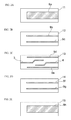
- FIG. 1A is a front sectional view of an ESD protective device according to a first embodiment of the present disclosure
- FIG. 1B is a plan sectional view of a substrate used in the first embodiment, i.e., a plan sectional view taken at a height position where first and second discharge electrodes are formed
- FIG. 1C is a sectional view taken along a line I-I in FIG. 1A .
- FIGS. 2A to 2E are each a plan view illustrating a ceramic green sheet that is prepared in manufacturing the ESD protective device according to the first embodiment, and one or more conductor patterns or electrode patterns, which are formed on the green sheet.
- FIG. 3 is a front sectional view of an ESD protective device according to a modification of the first embodiment.
- FIG. 4 is a transverse sectional view of an ESD protective device according to a second embodiment of the present disclosure.
- FIG. 5 is a transverse sectional view referenced to explain another modification of the ESD protective device of the present disclosure.
- FIG. 6 is a schematic sectional view illustrating still another modification of a conductor shape in the ESD protective device of the present disclosure.
- FIGS. 7A and 7B are respectively a schematic perspective view illustrating a relation between a substrate and a conductor used in an ESD protective device according to a third embodiment of the present disclosure, and a simplified transverse sectional view referenced to explain a structure of the conductor that is disposed inside the substrate.
- FIG. 1A is a front sectional view of an ESD protective device according to a first embodiment of the present disclosure
- FIG. 1C is a sectional view taken along a line I-I in FIG. 1A
- FIG. 1B is a plan sectional view of a substrate used in the first embodiment.
- An ESD protective device 1 includes a substrate 2 .
- the substrate 2 has a first principal surface 2 a and a second principal surface 2 b , the second principal surface 2 b being positioned on the side opposite to the first principal surface 2 a .
- the substrate 2 is in the form of a rectangular plate. It is to be noted that the shape of the substrate 2 is not limited to a rectangular plate.
- the substrate 2 can be made of an appropriate insulating material.
- the insulating material may be, for example, insulating ceramic, glass, or synthetic resin.
- the substrate 2 comprises a Low Temperature Co-fired Ceramic (LTCC) that is known as a BAS material containing Ba, Al and Si as main components.
- LTCC Low Temperature Co-fired Ceramic
- a metal having a low work function e.g., Cu or Ag
- a discharge start voltage can be further lowered.
- dielectric breakdown is harder to occur.
- a first discharge electrode 3 and a second discharge electrode 4 are formed in a plane that is located at a certain height position inside the substrate 2 . More specifically, as illustrated in the plan sectional view of FIG. 1B , the first discharge electrode 3 and the second discharge electrode 4 are opposed to each other in a plane 2 e , which is located at a certain height position inside the substrate 2 , in a spaced relation with a discharge gap G interposed therebetween. In this embodiment, a lateral side 3 a of the first discharge electrode 3 and a lateral side 4 a of the second discharge electrode 4 are opposed to each other in a spaced relation with the discharge gap G interposed therebetween.
- first and second discharge electrodes 3 and 4 may be opposed to each other in a spaced relation with the discharge gap interposed therebetween.
- the first and second discharge electrodes 3 and 4 can be each made of an appropriate metal, e.g., Ag or Cu, or an alloy containing one of those metals as a main component.
- a cavity A is formed inside the substrate 2 .
- a position of the cavity A is denoted by a dotted line in FIG. 1B .
- a region where the first and second discharge electrodes 3 and 4 are opposed to each other in a spaced relation with the discharge gap G interposed therebetween is positioned within the cavity A.
- An auxiliary electrode 5 is disposed within the cavity A.
- the auxiliary electrode 5 is disposed to lower a discharge start voltage.
- the auxiliary electrode 5 includes conductive particles 5 a coated with a material having no conductivity, and semiconductor ceramic particles 5 b .
- the auxiliary electrode 5 is disposed in a state connected to the discharge electrodes 3 and 4 .
- the first discharge electrode 3 is led out to a first end surface 2 c .
- the second discharge electrode 4 is led out to a second end surface 2 d .
- First and second outer electrodes 7 and 8 are formed to cover the first and second end surfaces 2 c and 2 d , respectively.
- the first and second outer electrodes 7 and 8 are each made of an appropriate conductive material.
- the first and second outer electrodes 7 and 8 can be each made of an appropriate metal, e.g., Ag or Cu.
- the first and second outer electrodes 7 and 8 may be each formed of a multilayer metallic film.
- a multilayer metallic film may be used in which a Ni film is laminated on an Ag film and a Sn alloy film having good solderability is laminated on an outer side surface of the Ni film.
- a conductor 9 is disposed inside the substrate 2 in a surrounding relation to the region where the discharge gap G is formed.
- the conductor 9 has the form of a rectangular ring, i.e., a rectangular frame, when viewed in a transverse section of the substrate 2 .
- the conductor 9 has a rectangular cylindrical shape.
- the discharge gap G and the region where the first and second discharge electrodes 3 and 4 are opposed to each other in a spaced relation with the discharge gap G interposed therebetween are both positioned within the rectangular cylindrical shape of the conductor 9 .
- the discharge start voltage can be effectively lowered as seen from an experimental example described later. Such an advantageous effect is attributable to the concentration of an electric field into the discharge gap.
- the conductor 9 is led out to the second end surface 2 d and is electrically connected to the second outer electrode 8 .
- the conductor 9 can be connected to the ground potential by connecting the second outer electrode 8 to the ground potential. With such grounding, the discharge start voltage can be further lowered. In addition, the heat generated near the discharge gap G can be rapidly dissipated through the second outer electrode 8 .
- the conductor 9 can be made of an appropriate metal.
- the metal constituting the conductor 9 is desirably the same as that constituting the first and second discharge electrodes 3 and 4 . In that case, since the number of the types of the metals used can be reduced, the manufacturing steps can be simplified.
- the conductor 9 can be formed by laminating sheets 11 to 15 illustrated in FIGS. 2A to 2E , for example, and firing the obtained multilayer body.
- the sheet 11 includes a conductor pattern 9 a penetrating through the sheet 11 .
- the sheet 12 includes conductor patterns 9 b and 9 c penetrating through the sheet 12 .
- the sheet 13 includes conductor patterns 9 d and 9 e penetrating through the sheet 13 .
- the first and second discharge electrodes 3 and 4 are printed on a ceramic green sheet that constitutes the sheet 13 .
- the materials constituting the auxiliary electrode 5 are also disposed in the gap G
- the sheet 14 illustrated in FIG. 2D , includes conductor patterns 9 f and 9 g penetrating through the sheet 14 .
- the sheet 15 illustrated in FIG. 2E , has the same structure as that of the sheet 11 illustrated in FIG. 2A .
- the sheet 15 includes a conductor pattern 9 h penetrating through the sheet 15 .
- the substrate 2 is obtained by firing the above-mentioned multilayer body.
- the first and second outer electrodes 7 and 8 may be formed on the end surfaces 2 c and 2 d of the substrate 2 , respectively, by a suitable method such as baking of a conductive paste or plating.
- the conductor 9 is led out to the second end surface 2 d , it is not necessary that the conductor 9 be led out to the second end surface 2 d as in an ESD protective device 21 according to a modification illustrated in FIG. 3 .
- the conductor 9 is constituted as a floating conductor without being electrically connected to the second outer electrode 8 . Also in that modification, the discharge start voltage can be lowered as in the first embodiment.
- a conductor 9 A having a circular ring shape in a transverse section may be disposed as represented by the conductor 9 A illustrated in FIG. 4 .
- the conductor 9 A has a substantially circular cylindrical shape inside the substrate 2 .
- the conductor may have a rectangular or circular ring sectional shape, when viewed in the transverse section of the substrate, around a portion where the discharge gap is provided.
- the conductor preferably has a circular ring sectional shape, i.e., a substantially circular cylindrical shape like the conductor 9 A.
- Such a shape is effective in reducing variations of influences attributable to different positions of the conductor depending on a direction relative to the discharge gap in the above-described section.
- a conductor 9 C has a transverse sectional shape resulting from removing one side of a rectangular frame.
- a conductor 9 D may have an L-like transverse sectional shape.
- the conductor in the present disclosure may have a transverse sectional shape fully surrounding the discharge gap.
- the conductor is just required to have a nonlinear shape in a section that extends in a direction interconnecting the first principal surface 2 a and the second principal surface 2 b of the substrate 2 , and that passes the discharge gap.
- the conductor may have, as illustrated in FIG. 6 , a portion 9 D 1 extending in a first direction, and a portion 9 D 2 extending in a second direction different from the first direction in which the portion 9 D 1 extends.
- a conductor 9 E may be used which is arranged inside the substrate 2 in a spiral shape.
- a part 9 E 1 of the conductor 9 E having the spiral shape is exposed to the illustrated section.
- a part 9 E 2 denoted by dotted lines, schematically illustrates a portion of the conductor 9 E extending in a direction toward the backside of the drawing sheet from the illustrated section.
- a part 9 E 3 denoted by one-dot-chain lines, schematically illustrates a portion of the conductor 9 E positioned on the side toward the front side of the drawing sheet from the part 9 E 1 that is exposed to the illustrated section.
- the conductor 9 E having the spiral shape can be formed by successively connecting a conductive film 9 E 4 and a via hole electrode 9 E 5 , which are illustrated in FIG. 7B .
- Ceramic slurry was prepared by adding an organic solvent, a binder resin, and a plasticizer to ceramic powder adapted for constituting a BAS material, and by mixing them.
- a ceramic green sheet with a thickness of 50 ⁇ m was obtained by shaping the ceramic slurry, prepared as described above, with a doctor blade method.
- a discharge electrode paste was prepared by adding an organic solvent to a mixture containing 80% by weight of Cu powder with an average particle diameter of 2 ⁇ m and 20% by weight of a binder resin made of ethyl cellulose, and by mixing them.
- auxiliary electrode paste used to form the auxiliary electrode was prepared. More specifically, the auxiliary electrode paste was prepared by mixing Cu powder coated with Al 2 O 3 , silicon carbide powder with an average particle diameter of about 1 ⁇ m, a binder resin, and an organic solvent. The Cu powder coated with Al 2 O 3 had an average particle diameter of about 2 ⁇ m. In the auxiliary electrode paste, a total of the Cu powder coated with Al 2 O 3 and the silicon carbide power occupied 80% by weight, and a total of the binder resin and the solvent occupied 20% by weight.
- the first and second discharge electrodes were formed by applying the auxiliary electrode paste and the discharge electrode paste on the sheet 13 made of the ceramic green sheet obtained as described above.
- Each of the first and second discharge electrodes had a width of 100 ⁇ m, and the discharge gap G had a size of 20 ⁇ m.
- Each of the lateral sides of the discharge electrodes positioned opposite to each other in a spaced relation with the discharge gap G interposed therebetween had a length of 150 ⁇ m.
- a resin paste was applied over a region where the discharge gap is to be formed.
- the conductor patterns 9 d and 9 e illustrated in FIG. 2C were formed by boring through holes in the ceramic green sheet with a laser, and by filling, into the through holes, an electrode paste that was similar to the paste used to form the discharge electrodes.
- the sheets 11 , 12 , 14 and 15 were prepared by forming the conductor patterns 9 a , 9 b , 9 c , 9 f , 9 g and 9 h , illustrated in FIGS. 2A, 2B, 2D and 2E , on the ceramic green sheets.
- a multilayer body was obtained by laminating the above-mentioned sheets 11 to 15 , and further laminating plain ceramic green sheets on the upper and lower sides of the laminated sheets.
- a multilayer body having a thickness of 0.3 mm was obtained.
- a multilayer body having dimensions of 1.0 mm ⁇ 0.5 mm ⁇ 0.3 mm in thickness i.e., the ESD protective device 1 per unit, was prepared.
- the outer electrodes 7 and 8 were formed by applying a conductive paste containing Cu powder as a main component to both the end surfaces of the substrate 2 , and by baking the applied conductive paste. A Ni plating layer and a Sn plating layer were further formed on each of the outer electrodes 7 and 8 .
- the ESD protective device 1 of the first embodiment was thus obtained.
- the ESD protective device of the second embodiment, illustrated in FIG. 4 was obtained in a similar manner to that in the above-described first embodiment except for using, instead of the above-described sheets 11 to 15 , a plurality of sheets including conductor patterns that were modified so as to form the conductor 9 A having the substantially circular cylindrical shape illustrated in the sectional view of FIG. 4 .
- an ESD protective device was fabricated in a similar manner to that in the above-described first embodiment except for not forming the conductor patterns 9 a to 9 h.
- Respective discharge start voltages of the ESD protective devices of the first and second embodiments and the comparative example, obtained as described above, were measured in conformity with the IEC standards, i.e., the electrostatic discharge immunity test specified in IEC61000-4-2.
- ⁇ The discharge test was carried out ten times for each of ten samples, and the discharge probability at the applied load voltage was 30 to 60%.
- the discharge test was carried out ten times for each of ten samples, and the discharge probability at the applied load voltage was 60% or more.
Landscapes
- Thermistors And Varistors (AREA)
Applications Claiming Priority (3)
| Application Number | Priority Date | Filing Date | Title |
|---|---|---|---|
| JP2013-142254 | 2013-07-08 | ||
| JP2013142254 | 2013-07-08 | ||
| PCT/JP2014/066422 WO2015005100A1 (ja) | 2013-07-08 | 2014-06-20 | Esd保護装置 |
Related Parent Applications (1)
| Application Number | Title | Priority Date | Filing Date |
|---|---|---|---|
| PCT/JP2014/066422 Continuation WO2015005100A1 (ja) | 2013-07-08 | 2014-06-20 | Esd保護装置 |
Publications (2)
| Publication Number | Publication Date |
|---|---|
| US20160104999A1 US20160104999A1 (en) | 2016-04-14 |
| US9780533B2 true US9780533B2 (en) | 2017-10-03 |
Family
ID=52279786
Family Applications (1)
| Application Number | Title | Priority Date | Filing Date |
|---|---|---|---|
| US14/972,517 Active 2034-11-13 US9780533B2 (en) | 2013-07-08 | 2015-12-17 | ESD protective device |
Country Status (4)
| Country | Link |
|---|---|
| US (1) | US9780533B2 (ja) |
| JP (1) | JP5884950B2 (ja) |
| CN (1) | CN105340141B (ja) |
| WO (1) | WO2015005100A1 (ja) |
Families Citing this family (1)
| Publication number | Priority date | Publication date | Assignee | Title |
|---|---|---|---|---|
| WO2016208383A1 (ja) | 2015-06-22 | 2016-12-29 | 株式会社村田製作所 | Esd保護装置およびesd保護装置の製造方法 |
Citations (4)
| Publication number | Priority date | Publication date | Assignee | Title |
|---|---|---|---|---|
| JP2003123936A (ja) | 2001-10-16 | 2003-04-25 | Matsushita Electric Ind Co Ltd | 電子部品およびその製造方法 |
| WO2008146514A1 (ja) | 2007-05-28 | 2008-12-04 | Murata Manufacturing Co., Ltd. | Esd保護デバイス |
| JP2010129323A (ja) | 2008-11-26 | 2010-06-10 | Murata Mfg Co Ltd | Esd保護デバイスの製造方法及びesd保護デバイス |
| US20110222197A1 (en) * | 2008-11-26 | 2011-09-15 | Murata Manufacturing Co., Ltd. | Esd protection device and method for manufacturing the same |
-
2014
- 2014-06-20 JP JP2015526240A patent/JP5884950B2/ja active Active
- 2014-06-20 CN CN201480037402.7A patent/CN105340141B/zh active Active
- 2014-06-20 WO PCT/JP2014/066422 patent/WO2015005100A1/ja active Application Filing
-
2015
- 2015-12-17 US US14/972,517 patent/US9780533B2/en active Active
Patent Citations (5)
| Publication number | Priority date | Publication date | Assignee | Title |
|---|---|---|---|---|
| JP2003123936A (ja) | 2001-10-16 | 2003-04-25 | Matsushita Electric Ind Co Ltd | 電子部品およびその製造方法 |
| WO2008146514A1 (ja) | 2007-05-28 | 2008-12-04 | Murata Manufacturing Co., Ltd. | Esd保護デバイス |
| US20090067113A1 (en) | 2007-05-28 | 2009-03-12 | Murata Manufacturing Co., Ltd. | Esd protection device |
| JP2010129323A (ja) | 2008-11-26 | 2010-06-10 | Murata Mfg Co Ltd | Esd保護デバイスの製造方法及びesd保護デバイス |
| US20110222197A1 (en) * | 2008-11-26 | 2011-09-15 | Murata Manufacturing Co., Ltd. | Esd protection device and method for manufacturing the same |
Non-Patent Citations (2)
| Title |
|---|
| Intemational Search Report issued in Application No. PCT/JP2014/066422 dated Sep. 9, 2014. |
| Translation of Written Opinion issued in Application No. PCT/JP2014/066422 dated Sep. 9, 2014. |
Also Published As
| Publication number | Publication date |
|---|---|
| JP5884950B2 (ja) | 2016-03-15 |
| CN105340141A (zh) | 2016-02-17 |
| US20160104999A1 (en) | 2016-04-14 |
| CN105340141B (zh) | 2017-03-15 |
| WO2015005100A1 (ja) | 2015-01-15 |
| JPWO2015005100A1 (ja) | 2017-03-02 |
Similar Documents
| Publication | Publication Date | Title |
|---|---|---|
| KR101392455B1 (ko) | Esd 보호 디바이스 및 그 제조 방법 | |
| US8711537B2 (en) | ESD protection device and method for producing the same | |
| US9590417B2 (en) | ESD protective device | |
| WO2011145598A1 (ja) | Esd保護デバイス | |
| JP5971416B2 (ja) | Esd保護装置 | |
| JP5649391B2 (ja) | Esd保護デバイス | |
| US20160056627A1 (en) | Esd protection device | |
| US9780533B2 (en) | ESD protective device | |
| US20140376147A1 (en) | Esd protection device | |
| JP2009117735A (ja) | 静電気対策部品およびその製造方法 | |
| JP5874743B2 (ja) | Esd保護装置 | |
| US20180098410A1 (en) | Esd protection device | |
| US9837795B2 (en) | ESD protection device | |
| JP6079880B2 (ja) | Esd保護装置 | |
| JP6075447B2 (ja) | Esd保護装置 | |
| US10320154B2 (en) | ESD protection device and manufacturing method for ESD protection device | |
| JP6428938B2 (ja) | Esd保護装置 | |
| JP6048055B2 (ja) | Esd保護デバイスとその製造方法 | |
| JP5614563B2 (ja) | Esd保護デバイスの製造方法 | |
| WO2017036511A1 (en) | Electric multilayer component for surface-mount technology and method of producing an electric multilayer component | |
| JP2010097791A (ja) | 過電圧保護部品 | |
| JP2014235987A (ja) | Esd保護装置の製造方法及びesd保護装置 | |
| JP2018535510A (ja) | 過電圧保護デバイスおよび過電圧保護デバイスを製造するための方法 |
Legal Events
| Date | Code | Title | Description |
|---|---|---|---|
| AS | Assignment |
Owner name: MURATA MANUFACTURING CO., LTD., JAPAN Free format text: ASSIGNMENT OF ASSIGNORS INTEREST;ASSIGNORS:YASUNAKA, KATSUMI;ADACHI, JUN;TSUKIZAWA, TAKAYUKI;SIGNING DATES FROM 20151203 TO 20151204;REEL/FRAME:037316/0164 |
|
| STCF | Information on status: patent grant |
Free format text: PATENTED CASE |
|
| MAFP | Maintenance fee payment |
Free format text: PAYMENT OF MAINTENANCE FEE, 4TH YEAR, LARGE ENTITY (ORIGINAL EVENT CODE: M1551); ENTITY STATUS OF PATENT OWNER: LARGE ENTITY Year of fee payment: 4 |