US9698680B2 - Switching power device - Google Patents
Switching power device Download PDFInfo
- Publication number
- US9698680B2 US9698680B2 US14/852,705 US201514852705A US9698680B2 US 9698680 B2 US9698680 B2 US 9698680B2 US 201514852705 A US201514852705 A US 201514852705A US 9698680 B2 US9698680 B2 US 9698680B2
- Authority
- US
- United States
- Prior art keywords
- voltage
- circuit
- output
- control unit
- soft
- Prior art date
- Legal status (The legal status is an assumption and is not a legal conclusion. Google has not performed a legal analysis and makes no representation as to the accuracy of the status listed.)
- Active
Links
Images


Classifications
-
- H—ELECTRICITY
- H02—GENERATION; CONVERSION OR DISTRIBUTION OF ELECTRIC POWER
- H02M—APPARATUS FOR CONVERSION BETWEEN AC AND AC, BETWEEN AC AND DC, OR BETWEEN DC AND DC, AND FOR USE WITH MAINS OR SIMILAR POWER SUPPLY SYSTEMS; CONVERSION OF DC OR AC INPUT POWER INTO SURGE OUTPUT POWER; CONTROL OR REGULATION THEREOF
- H02M3/00—Conversion of dc power input into dc power output
- H02M3/02—Conversion of dc power input into dc power output without intermediate conversion into ac
- H02M3/04—Conversion of dc power input into dc power output without intermediate conversion into ac by static converters
- H02M3/10—Conversion of dc power input into dc power output without intermediate conversion into ac by static converters using discharge tubes with control electrode or semiconductor devices with control electrode
- H02M3/145—Conversion of dc power input into dc power output without intermediate conversion into ac by static converters using discharge tubes with control electrode or semiconductor devices with control electrode using devices of a triode or transistor type requiring continuous application of a control signal
- H02M3/155—Conversion of dc power input into dc power output without intermediate conversion into ac by static converters using discharge tubes with control electrode or semiconductor devices with control electrode using devices of a triode or transistor type requiring continuous application of a control signal using semiconductor devices only
- H02M3/156—Conversion of dc power input into dc power output without intermediate conversion into ac by static converters using discharge tubes with control electrode or semiconductor devices with control electrode using devices of a triode or transistor type requiring continuous application of a control signal using semiconductor devices only with automatic control of output voltage or current, e.g. switching regulators
-
- H—ELECTRICITY
- H02—GENERATION; CONVERSION OR DISTRIBUTION OF ELECTRIC POWER
- H02M—APPARATUS FOR CONVERSION BETWEEN AC AND AC, BETWEEN AC AND DC, OR BETWEEN DC AND DC, AND FOR USE WITH MAINS OR SIMILAR POWER SUPPLY SYSTEMS; CONVERSION OF DC OR AC INPUT POWER INTO SURGE OUTPUT POWER; CONTROL OR REGULATION THEREOF
- H02M1/00—Details of apparatus for conversion
- H02M1/36—Means for starting or stopping converters
Definitions
- the present disclosure relates to a switching power device.
- a soft-start circuit is occasionally included in this type of switching power device.
- the soft-start circuit is arranged for preventing a large rush current from flowing into a switching element (for example, see Patent Document 1).
- a soft-start is carried out in response to an input terminal voltage.
- it is possible to prevent a rush current from damaging a switching element.
- the technology disclosed in the Patent Document 1 reads only an input terminal voltage, the technology effectively operates at the time of activating the input terminal voltage.
- the technology disclosed in the Patent Document 1 cannot be applied to the situation where the output terminal voltage suddenly drops in response to some events after the activation of the input terminal voltage and to the situation where the output terminal voltage drops as the input terminal voltage is not affected by the events.
- Patent Document 2 activates a soft-start circuit with reference to an output voltage, and inhibits an overshoot at the time of activating a power source.
- the technology in the Patent Document 2 discloses an invention for inhibiting an overshoot at the time of activating a power source. Even when this type of soft-start circuit is applied to the situation when the output terminal voltage suddenly drops from a reference voltage and returns to a restoration voltage, it may not be applicable in view of the properties of discharging voltage from a capacitor in, for example, a soft-start circuit.
- a switching power device includes: a main circuit that includes a switching element and a coil, and adjusts a current flowing through the coil and outputs a voltage in response to a driving signal; an output voltage detection circuit that outputs a first voltage corresponding to the voltage outputted from the main circuit; an error amplification circuit that outputs an error signal in response to a difference between the first voltage of the output voltage detection circuit and a second voltage corresponding to a control target voltage of the main circuit; an oscillation circuit that outputs an oscillation signal; a driving circuit that outputs the driving signal to the switching element in response to a comparison result obtained by comparing the oscillation signal of the oscillation circuit and the error signal of the error amplification circuit; and a soft-start control unit that controls the second voltage, which is provided to the error amplification circuit, to be a restart voltage between a control standard voltage, which corresponds to a target output voltage of the main circuit, and a control start voltage of the main circuit in response to the first voltage of the output voltage detection circuit
- the soft-start control unit controls the second voltage, which is provided to the error amplification circuit, to be the restart voltage between the control standard voltage corresponding to the target output voltage of the main circuit and the control start voltage of the main circuit in response to the first voltage of the output voltage detection circuit, a soft-start can be carried out so that an overshoot can be inhibited when the output terminal voltage suddenly drops from the standard output voltage as the target output voltage and then returns to the restoration voltage.
- FIG. 1 is a diagram that shows an electrical configuration of a switching power device schematically
- FIG. 2 is a graph that shows a waveform chart illustrating the relationship among an output signal of an error amplification circuit, an oscillation signal of an oscillation circuit, and an output of an comparator;
- FIG. 3 is a diagram that shows an electrical configuration schematically illustrating an example of the configuration of an input stage in the error amplification circuit
- FIG. 4 is a diagram that shows an electrical configuration schematically illustrating a soft-start control unit
- FIG. 5 is a diagram that shows an electrical configuration schematically illustrating a main control unit
- FIG. 6 is a graph that shows a timing chart schematically illustrating the relationship between the waveform of an input voltage and the waveform of an output voltage
- FIGS. 7A and 7B are graphs that show characteristic charts schematically illustrating the relationship between an input signal and an output signal of a logic circuit
- FIGS. 8A through 8C are graphs that show timing charts schematically illustrating the flow of a soft-start control process when the output voltage changes;
- FIG. 9 is a graph that is a timing chart schematically illustrating the flow of a control process when the output voltage changes to a degree in which the output voltage does not reach a threshold value
- FIGS. 10A through 10C are graphs that show timing charts schematically illustrating the flow of controlling a step time at the time of performing a soft-start control
- FIG. 11 is a diagram that shows an electrical configuration schematically illustrating one modification example of the schematic configuration of an oscillation unit
- FIG. 12 is a diagram that shows an electrical configuration schematically illustrating a soft-start control unit according to a second embodiment.
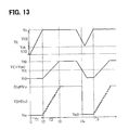
- FIG. 13 is a diagram that shows a timing chart schematically illustrating the flow of a soft-start control process when the output voltage changes.
- a switching power device 1 described in the following section illustrates a mode of a positive power circuit for controlling an output voltage Vout from 0V before activation to a positive predetermined voltage after activation; however, the embodiment is applicable to a negative power circuit for controlling the output voltage Vout from 0V before activation to a negative predetermined voltage after activation.
- FIG. 1 shows an example of the configuration of a switching power device 1 .
- the switching power device 1 is a step-down type configuration and is configured to connect a pre-drive circuit 2 as a driving circuit, a MOS transistor 3 for output as a switching element, a boot-strap capacitor 4 , a reflux diode 5 , a coil 6 , a capacitor 7 , resistors 8 and 9 , a reference voltage generating circuit 10 , an error amplification circuit 11 , an oscillation circuit 12 , a comparator 13 and a soft-start control unit 14 .
- the switching power device 1 has an output terminal to which a load 15 is connected.
- the reference voltage generating circuit 10 the error amplification circuit 11 , the oscillation circuit 12 , the comparator 13 and the soft-start control unit 14 constitute a control unit 100 of the switching power device 1 .
- the MOS transistor 3 is configured as a main-drive switching circuit through, for example, an n-channel type MOSFET.
- the switching circuit may be configured by a p-channel type MOSFET, or may be configured by other kinds of transistor such as a bipolar transistor.
- a battery voltage VB 1 or the like as an input voltage Vin is provided to the drain of the MOS transistor 3 , and the reflux diode 5 is connected between the source of the MOS transistor 3 and a ground.
- the pre-drive circuit 2 is connected to the gate of the MOS transistor 3 .
- the pre-drive circuit 2 sends a driving signal to the part between the gate and the source of the MOS transistor 3 in response to a control signal provided from a preceding circuit (i.e., the comparator 13 ) of the pre-drive circuit 2 .
- the boot-strap capacitor 4 is connected between the MOS transistor 3 and the pre-drive circuit 2 so that it is possible to perform quick charging.
- the coil 6 is connected between the source of the MOS transistor 3 and the output terminal OUT.
- the capacitor 7 is connected between the output terminal OUT and the ground.
- the pre-drive circuit 2 controls the MOS transistor 3 to turn off, in order to maintain the flowing current in the coil 6 , the current flows in a reflux loop composed by the coil 6 , the reflux diode 5 and the load 15 and the output voltage Vout lowers when the power held in the capacitor 7 is discharged.
- Voltage dividing resistors 8 , 9 are connected between the output terminal OUT and the ground.
- the voltage dividing resistors 8 , 9 divide the output voltage Vout and output the voltage V 1 to the inverting input terminal of an op-amp 11 a .
- the error amplification circuit 11 includes the op-amp 11 a and a feedback resistor 11 b connected between the inverting input terminal and the output terminal of the op-amp 11 a.
- the reference voltage generating circuit 10 and the soft-start control unit 14 are connected to the non-inverting input terminal of the op-amp 11 a .
- the reference voltage generating circuit 10 is configured by, for example, a band-gap reference circuit to generate a reference voltage Vref with high precision, and outputs the reference voltage Vref to the non-inverting input terminal of the op-amp 11 a in the error amplification circuit 11 .
- the soft-start control unit 14 uses a D/A converter 21 illustrated in FIG. 4 to output a D/A output control voltage Vdac.
- the error amplification circuit 11 amplifies the difference between the dividing voltage V 1 obtained from the output voltage Vout through the resistors 8 , 9 , and either the output reference voltage Vref of the reference voltage generating circuit 10 or the D/A output control voltage Vdac of the soft-start control unit 14 and then outputs the result.
- FIG. 3 illustrates an example of the configuration of an input stage of the op-amp 11 a in the error amplification circuit 11 .
- the op-amp 11 a ordinarily constitutes, for example, an amplification stage and an output stage, however, the drawings of these stages are omitted.
- the op-amp 11 a includes a current source 18 , pnp-type transistors Tr 1 through Tr 3 , and npn-type transistors Tr 4 and Tr 5 .
- the pnp-type transistors Tr 1 through Tr 3 are connected in parallel and constitute differential pairs.
- the npn-type transistors Tr 4 and Tr 5 are connected as a current mirror to form an active load in response to the differential pairs.
- the reference voltage Vref outputted from the reference voltage generating circuit 10 is applied to the base of the pnp-type transistor Tr 1 , and the D/A output control voltage Vdac of the soft-start control unit 14 is applied to the base of the pnp-type transistor Tr 2 .
- the dividing voltage V 1 obtained by dividing the output voltage Vout is applied to the base of the pnp-type transistor Tr 3 .
- the control voltage Vdac is less than the reference voltage Vref
- the voltage V 1 i.e., the base voltage of the pnp-type transistor Tr 3
- the collector current of the pnp-type transistor Tr 3 increases in response to ⁇ V
- the output voltage of the active load Tr 5 increases in response to the increment portion of the collector current.
- the input stage of the op-amp 11 a outputs the amplified voltage Vz as a result of the amplification of the difference between the control voltage Vdac and the voltage V 1 .
- the input stage of the op-amp 11 a output the voltage Vz as a result of the amplification of the difference between the reference Vref and the voltage V 1 .
- the error amplification circuit 11 amplifies the output voltage Vz of the input stage of the op-amp 11 a through the amplification stage and the output stage, and outputs to the comparator 13 as the voltage V 3 .
- the op-amp 11 a is configured by using the pnp-type transistors Tr 1 through Tr 3 and the npn-type transistors Tr 4 and Tr 5 ; however, p-channel type MOS transistors and n-channel type MOS transistors may be used in replace of the pnp-type transistors and the npn-type transistors.
- the voltage V 3 outputted from the error amplification circuit 11 is provided to the non-inverting input terminal of the comparator 13 .
- the oscillation circuit 12 is connected to the inverting input terminal of the comparator 13 .
- the comparator 13 outputs an oscillation signal that changes in a predetermined cycle formed in, for example, a triangular waveform or a saw-tooth waveform.
- the comparator 13 outputs a comparison result obtained by comparing the output signal of the error amplification circuit 11 and the oscillation signal of the oscillation circuit 12 .
- the MOS transistor 3 , the reflux diode 5 , the coil 6 , the capacitor 7 constitutes a main circuit 16
- the resistors 8 , 9 constitutes an output voltage detecting circuit 17 .
- FIG. 2 schematically shows a comparison result obtained by comparing the output signal of the error amplification circuit 11 and the oscillation signal of the oscillation circuit 12 .
- the comparator 13 when the output signal of the error amplification circuit 11 is higher than the oscillation signal of the oscillation circuit 12 , the comparator 13 outputs an “H”-level signal; and when the output signal of the error amplification circuit 11 is lower than the oscillation signal of the oscillation circuit 12 , the comparator 13 outputs an “L”-level signal.
- the comparator 13 outputs, for example, a PWM signal with higher proportion of “L”-level.
- the comparator 13 when the voltage V 3 outputted from the error amplification circuit 11 is higher, the comparator 13 outputs, for example, a PWM signal with higher proportion of “H”-level.
- the PWM signal is provided to the pre-drive circuit 2 .
- the pre-drive circuit 2 applies a voltage larger than a threshold voltage between the gate and source of the MOS transistor 3 when the PWM signal sent from the comparator 13 is at the “H”-level; and the pre-drive circuit 2 applies a voltage (i.e., 0 volt) smaller than the threshold voltage between the gate and source of the MOS transistor 3 when the PWM signal is at the “L”-level. Therefore, the pre-drive circuit 2 control the MOS transistor 3 to turn on or off in response to the PWM signal.
- the duty ratio of the PWM signal changes in response to the magnitude of the voltage V 3 outputted from the error amplification circuit 11 so that the output voltage Vout is controlled so as to conform to the target output voltage.
- the soft-start control unit 14 includes a main control unit 20 , a D/A converter 21 and an oscillation unit 22 .
- the D/A converter 21 includes a counter 23 , a DAC core 24 , OR gates 25 , 26 .
- the voltage outputted from the DAC core 24 is configured as the output control voltage Vdac, and is outputted to the error amplification circuit 11 .
- the oscillation unit 22 is configured such that resistors 28 , 29 are connected to the input and output of an inverter 27 , and is configured by a self-oscillator connecting a capacitor 30 , which is connected between the input of the inverter 27 and the ground.
- the resistors 28 , 29 connected between the input and output terminals of the inverter 27 are connected in parallel.
- the resistance values of the resistors 28 , 29 are set to be different to each other, and switches 31 , 32 for selecting the resistor 28 or the resistor 29 are respectively connected to the resistors 28 , 29 .
- the switches 31 , 32 enable the main control unit 20 to perform on/off control. Accordingly, the oscillation frequency of the oscillation unit 22 can be controlled by the main control unit 20 , and the oscillation unit 22 outputs an oscillation signal, whose frequency is controlled by the main control unit 20 , as a clock signal CK to the counter 23 in the D/A converter 21 after power activation.
- the counter 23 is configured by connecting a plurality (i.e., n-stages) of DFFs 33 through 38 in a cascade form.
- the DFFs 33 through 38 are configured such that the inputs D are connected to the inverting outputs QB.
- Each of the DFFs 33 through 38 configures the QB output at the pre-stage circuit as a clock input and maintains the output Q and the inverting output QB at the QB output timing.
- the DFF 33 as the 1 st stage performs inversion at the output timing of the clock signal CK
- the DFFs 34 through 38 as the k th (n ⁇ k ⁇ 2) stage perform inversion at the output timing of the DFFs 33 through 37 as the (k ⁇ 1) th stage.
- the counter 23 adds 1 when the clock signal CK at “1” is inputted.
- the DAC core 24 converts k-bit digital data of the counter 23 as an analog signal and outputs the signal as a D/A output control voltage Vdac at the input timing in which an input clock signal CK is inputted.
- the main control unit 20 is configured by, for example, the control logic as shown in FIG. 5 , and the main control unit 20 inputs an input voltage Vin, an output voltage Vout, and a clock signal CK and outputs control signals SW 1 and SW 2 sent from the switches 31 , 32 , restart signals RSTA 1 , RSTA 2 , and a reset signal RST based on the input signal.
- the OR gates 26 , 25 are respectively connected to digital input terminals DINn-1, DINn-2 at the upper two-bits on an MSB side of the DAC core 24 .
- the OR gate 26 inputs the output Q of the DFF 38 corresponding to MSB and the restart signal RSTA 2 inputted from the main control unit 20 , and outputs the result of the logical operation to the digital input terminal DINn-1 as the MSB of the DAC core 24 .
- the OR gate 25 inputs the output Q of the DFF 37 corresponding to the MSB-1 bit and the restart signal RSTA 1 inputted from the main control unit 20 , and outputs the result of the logical operation to the digital input terminal DINn- 2 corresponding to the MSB-1 bit of the DAC core 24 .
- the OR gate 26 When the OR gate 26 inputs the restart signal RSTA 2 at an active level “1” (i.e., “H” in the present embodiment), the OR gate 26 compulsorily outputs the signal at the active level “1” (i.e., “H” in the present embodiment) to the digital input terminal DINn-1 of the DAC core 24 .
- the OR gate 25 When the OR gate 25 inputs the restart signal RSTA 1 at the active level “1,” the OR gate 25 compulsorily outputs the signal at the active level “1” to the digital input terminal DINn-2 of the DAC core 24 . Therefore, the main control unit 20 controls the restart signals RSTA 1 , RSTA 2 to enable the output voltage Vdac of the DAC core 24 to be controlled step by step instantaneously.
- the main control unit 20 outputs the reset signal RST to the reset terminal of each of the DFFs 33 through 38 in the counter 23 .
- the reset signal RST is at the active level, the counter 23 resets itself and restarts the counting from zero.
- the main control unit 20 switches the restart signals RSTA 1 , RSTA 2 as the active level “1” or the inactive level “0” and outputs the reset signal RST at the active level “1” to the counter 23 so as to control the count value of the counter 23 to be inputted to the DAC core 24 and controls the D/A output control voltage Vdac to be at 0 volts, a quarter, an half, and three quarters of the maximum limiting voltage of the voltage Vdac step by step instantly
- FIG. 5 illustrates an example of circuit configuration of the main control unit 20 schematically.
- the main control unit 20 is configured by using, for example, hysteresis-type comparators 40 through 43 , a logic circuit 44 , resistors 45 through 52 , and a NAND gate 53 , and becomes a module to input the input voltage Vin, the output voltage Vout and the clock signal CK and output the reset signal RST to the counter 23 based on these input signals to reset the counter 23 and controls the oscillation frequency of the oscillation unit 22 by controlling the switches 31 and 32 to turn on or off inside the oscillation unit 22 .
- the input voltage detection circuit 17 b detects a dividing voltage Vin 1 obtained by dividing the input voltage Vin through the resistors 45 and 46 .
- the output voltage detection circuit 17 detects the dividing voltages Vol through Vo 3 obtained by dividing the output voltage Vout through the resistors 47 through 52 .
- the comparators 40 through 43 inside the main control unit 20 have hysteresis input/output characteristic respectively.
- the output level i.e., SW 1 , SW 2 , RSTA 1 , RSTA 2
- the logic circuit 44 can be altered as illustrated in the after-mentioned FIG. 7 at the time when the input voltage Vin or the output voltage Vout rises and drops.
- the hysteresis-type comparator 40 compares a detection voltage of the input voltage detection circuit 17 b with the reference voltage Vref 1 , and outputs the comparison result to the logic circuit 44 .
- the hysteresis-type comparators 41 through 43 compare a detection voltage of the output voltage detection circuit 17 with reference voltages Vref 2 through Vref 4 respectively, and output the comparison results to the logic circuit 44 .
- the reference voltages Vref 2 through Vref 4 are set in the relation of Vref 2 >Vref 3 >Vref 4 .
- FIG. 6 illustrates the mode of changes in the input voltage Vin and the output voltage Vout.
- the output voltage Vout rises behind the rising change in the input voltage Vin.
- the output voltage Vout drops behind the dropping change in the input voltage Vin.
- the logic circuit 44 inside the main control unit 20 outputs the reset signal RST, and the restart signals RSTA 1 , RSTA 2 as shown in FIGS. 7A and 7B in response to the relationship between the input voltage Vin and the voltage V 1 (i.e., the output voltage Vout).
- FIG. 7A shows an example of the output logic level of the logic circuit 44 when the input voltage Vin or the output voltage Vout rises
- FIG. 7B shows an example of the output logic level of the logic circuit 44 when the input voltage Vin or the output voltage Vout drops.
- the reset signal RST in FIGS. 7A and 7B “1” represents the active level, and “0” represents the inactive level.
- the restart signals RSTA 1 and RSTA 2 are at “H”-level.
- the logic circuit 44 determines whether the output voltage V 1 of the output voltage detection circuit 17 exists in either a plurality of ranges divided step by step in order to change the reset signal RST, the restart signal RSTA 1 , RSTA 2 at the active level in response to the result of the logical operation, and outputs these signals as the control signals to the counter 23 or the OR gates 25 , 26 .
- the main control unit 20 controls to change the recounting value of the counter 23 to be inputted to the DAC core 24 in response to the result of the logical operation of the logic circuit 44 so as to generate restart voltages Vrs 1 , Vrs 2 , Vrs 3 of the output control voltage Vdac through the DAC core 24 .
- FIGS. 8A through 8C show three types of modes that illustrate: the moment when the output voltage Vout rises from the start voltage ( ⁇ start detection voltage Vs 0 ) at the time of an input voltage being applied, up to the standard control voltage ( ⁇ standard detection voltage Vt 0 ) at the time in which the output voltage is controlled normally; and the moment when the output voltage Vout suddenly drops from the standard control voltage.
- FIGS. 8A through 8C show three types of modes that illustrate: the moment when the output voltage Vout rises from the start voltage ( ⁇ start detection voltage Vs 0 ) at the time of an input voltage being applied, up to the standard control voltage ( ⁇ standard detection voltage Vt 0 ) at the time in which the output voltage is controlled normally; and the moment when the output voltage Vout suddenly drops from the standard control voltage.
- the battery voltage VB 1 is inputted in response to, for example, engine activation, the input voltage Vin rises based on the battery voltage VB 1 during T 1 period after the time t 1 in FIGS. 8A through 8C .
- an operational source voltage Vcc is provided to each of the circuits.
- the main control unit 20 controls an output of the clock signal CK at a prescribed frequency from the oscillation unit.
- the output voltage detection circuit 17 detects a start detection voltage VS 0 ( ⁇ 0 V) as the voltage V 1 obtained by dividing the output voltage Vout through the resistors.
- the input voltage Vin is lower than the start threshold voltage Vsin. Subsequently, during the time in which the input voltage Vin has not reached the start threshold voltage Vsin and the input voltage Vin is in the voltage range VH 2 , the main control unit 20 in the soft-start control unit 14 continues to output the active level “1” as the reset signal RST through the logic circuit as shown in FIG. 7A so as to continue resetting the output of the counter 23 . In other words, the output voltage Vout is controlled not to rise.
- the counter 23 is in an idle state by maintaining the counting value as 0 (i.e., T 1 period in FIGS. 8A through 8C ).
- the logic circuit 44 releases the reset as the inactive level “0,” and the main control unit 20 starts the original soft-start control at the time t 2 in FIG. 8 .
- the output of the error amplification circuit 11 is lower than the output of the oscillation circuit 12 (the inverting of the comparator 13 ).
- the control target voltage V 2 as the output voltage Vdac of the DAC core 24 rises step by step periodically.
- the output voltage Vout and the voltage V 1 also gradually rise to follow the control target voltage V 2 .
- the dividing voltage V 1 obtained through the resistors 8 , 9 gradually rises from the start detection voltage Vs 0 to the standard detection voltage Vt 0 during the T 2 period in FIG. 8 .
- the error amplification circuit 11 when the voltage Vdac is lower than the output reference voltage Vref of the reference voltage generating circuit 10 , the error amplification circuit 11 outputs the voltage reflecting the amplification of the error in response to the difference between the voltage Vdac and the voltage V 1 ; in contrary, when the voltage Vdac is higher than the output reference voltage Vref of the reference voltage generating circuit 10 , the error amplification circuit 11 outputs the voltage reflecting the amplification of the error in response to the difference between the output reference voltage Vref and the voltage V 1 of the reference voltage generating circuit 10 (see the above-mentioned description of FIG. 3 ).
- the switching power device 1 prevents an overshoot of the output voltage Vout as the control target voltage V 2 gradually rises with the lapse of time from the time t 2 right after activation to the time t 3 .
- the present disclosure considers the situation where the output voltage Vout of the output terminal OUT drops in an instant in response to some events. For example, the present disclosure considers some events such as a rapid change in the impedance value of the load 15 connected to the output terminal OUT, or the output terminal OUT having contact with a foreign substance and short-circuited to the ground.
- the present disclosure considers the situation where the output voltage Vout of the output terminal OUT drops at the time t 4 shown in FIG. 8 (see the voltage V 1 in FIGS. 8A through 8C ).
- the main control unit 20 of the soft-start control unit 14 compares the dividing voltage Vin 1 of the input voltage detection circuit 17 b with the voltage Vref through the comparator 40 , and compares the dividing voltages Vol through Vo 3 of the output voltage detection circuit 17 b with the voltages Vref 1 through Vref 3 through the comparators 41 through 43 respectively.
- the comparison result in which the main control unit 20 uses the comparators 40 through 43 is described in reference to FIG. 8 describing the input voltage Vin and the voltage V 1 proportional to the output voltage Vout as the base.
- the comparison result performed by the comparator 40 corresponds to the concept of determining whether the input voltage Vin exists in the input voltage range VH 1 or the input voltage range VH 2 .
- the comparison processes performed by the comparators 41 through 43 correspond to the concept of comparing the voltage V 1 corresponding to the output voltage Vout with the soft-start threshold voltages Vt 1 through Vt 3 .
- the threshold voltages Vt 1 through Vt 3 are preliminarily set to correspond to the voltages Vref 2 through Vref 4 shown in FIG.
- threshold voltages Vt 1 through Vt 3 are used as the soft-start threshold voltages as the determination threshold values to determine whether the output voltage Vout exists in either the output voltage range VA, VB, VC or VD shown in FIG. 6 . Since the voltage V 1 is proportional to the output voltage Vout, the following describes the situation of using the relationship between the voltage V 1 and the soft-start threshold voltages Vt 1 through Vt 3 .
- the control target voltage V 2 at this time is larger than the output reference voltage Vref of the reference voltage generating circuit 10 .
- the input voltage Vin is in the voltage range VH 1 , and the voltage V 1 is nearly stable at the standard detection voltage Vt 0 so that the output voltage Vout is within the voltage range VA shown in FIG. 6 .
- the logic circuit 44 outputs the inactive level “0” as the reset signal RST and outputs the “L”-level to the OR gates 26 , 25 as the signals RSTA 1 , RSTA 2 as shown in FIGS. 7A and 7B .
- the DAC core 24 outputs the control target voltage V 2 in response to the output of the counter 23 .
- the soft-start control unit 14 controls the changing of the output of the counter 23 to be inputted to the DAC core 24 so as to lower the output voltage Vdac so that the voltage V 2 is set at the restart voltage Vrs 1 , Vrs 2 and Vrs 3 step by step (see the time t 4 shown in FIGS. 8A through 8C ).
- the restart voltages Vrs 1 through Vrs 3 are set in relation of Vrs 1 >Vrs 2 >Vrs 3 in the present embodiment.
- the logic circuit 44 outputs the active level “1” as the reset signal RST in a pulse-shape form, and outputs the “H”-level as the signals RSTA 1 , RSTA 2 to the OR gates 26 , 25 .
- the DAC core 24 outputs approximately three quarters of the reference voltage Vref ( ⁇ control standard voltage Vty) as the restart voltage Vrs 1 for the output voltage Vdac of the DAC core 24 .
- the DAC core 24 controls the output voltage Vdac to rise gradually in reference to the restart voltage Vrs 1 (see the T 5 period in FIG. 8A ).
- the control target voltage V 2 is stabilized at the reference voltage Vref (see the T 6 period in FIG. 8A ).
- the comparators 41 , 42 among the comparators 41 through 43 outputs the “L”-level, and the comparator 43 outputs the “H”-level.
- the logic circuit 44 outputs the active level “1” as the reset signal RST in a pulse-shape form, and outputs the “H”-level as the signal RSTA 1 to the OR gate 26 .
- the DAC core 24 controls the output voltage Vdac to rise gradually in reference to the restart voltage Vrs 2 (see the T 5 period in Hg. 8 B).
- the control target voltage V 2 is stabilized at the reference voltage (see the T 6 period in FIG. 8B ).
- the comparators 41 through 43 output the “L”-level altogether.
- the logic circuit 44 outputs the active level “1” as the reset signal RST in a pulse-shape form, and outputs the “L”-level as the signals RSTA 1 , RSTA 2 to the OR gates 26 , 25 .
- the counting result of the counter 23 is once reset and the “L”-level is inputted to the OR gates 26 , 25 , the counting result of the counter 23 is inputted to all input bits of the DAC core 24 . Accordingly, the DAC core 24 outputs the control start voltage Vcs (for example, ⁇ 0V) as the restart voltage Vrs 3 for the output voltage Vdac of the DAC core 24 . Subsequently, even when the counter 23 restarts counting, all bits are made effective by the DFFs 33 through 38 of the counter 23 and are inputted to the DAC core 24 .
- Vcs for example, ⁇ 0V
- the DAC core 24 controls the output voltage Vdac to rise gradually in reference to the control start voltage Vcs as the restart voltage Vrs 3 (see the T 5 period in FIG. 8C ). Subsequently, when the DAC core 24 controls the output voltage Vdac to rise up to the control standard voltage Vty, the control target voltage V 2 is stabilized at the reference voltage Vref (see the T 6 period in FIG. 8C ).
- the main control unit 20 maintains the output voltage Vdac of the DAC core 24 constantly as the maximum value (the reference voltage Vref ⁇ the control standard voltage Vty) during the T 3 period in FIG. 9 . Therefore, the control target voltage V 2 does not change. The forgoing control is carried out.
- the soft-start control unit 14 controls the voltage V 2 provided to the error amplification circuit 11 to be at the restart voltages Vrs 1 , Vrs 2 and Vrs 3 located between the control standard voltage Vty corresponding to the target output voltage of the main circuit 16 and the control start voltage Vcs of the main circuit 16 , in response to the output voltage V 1 of the output voltage detection circuit 17 . Accordingly, the soft-start can be carried out even after the output voltage Vout drops so that a rush-in current can be inhibited and hence overshoot along with the rush-in current can be prevented. As a result, the fault such as the damage of elements can be prevented.
- the soft-start control unit 14 controls the restart voltages Vrs 1 , Vrs 2 and Vrs 3 step by step, the time until the return of the output voltage Vout can be adjusted in comparison to the case where the restart voltage is not controlled step by step.
- the soft-start control unit 14 includes the logic circuit 44 inside the main control unit 20 of the soft-start control unit 14 , and the logic circuit 44 determines whether the dividing voltages Vol through Vo 3 obtained by the output voltage Vout exist in the multiple voltage ranges VA, VB, VC or VD, which are divided step by step.
- the main control unit 20 uses, for example, the OR gates 26 , 25 can set the recount start value of the DAC core 24 at a plurality of different values; therefore, the restart voltages Vrs 1 , Vrs 2 and Vrs 3 can be set at different values so that the restart voltages Vrs 1 , Vrs 2 and Vrs 3 can be set without using an analog circuit.
- FIGS. 10A through 10C and FIG. 11 schematically illustrate a modification example.
- the main control unit 20 illustrated in FIG. 4 controls the switches 31 and 32 inside the oscillation unit 22 to turn on or off so as to enable the change of the output frequency (i.e., cycle) of the clock signal CK.
- the main control unit 20 adjusts the total resistance values of the resistors 28 , 29 connected in parallel to the input and output terminals of the inverter 27 inside the oscillation unit 22 to enable the control of the oscillation frequency, the adjustment of the output cycle of the clock signal CK can be achieved. Consequently, the counting period of the counter 23 can be adjusted.
- the counting-up period of the counter 23 shown in FIG. 10A is set as the standard count period Tc 1 , it takes only time Rd 1 for raising the control target voltage V 2 from the control start voltage Vcs to the control standard voltage Vty.
- the main control unit 20 adjusts the counting-up period of the counter 23 and shorten the counting-up period from the counting period Tc 1 to the counting period Tc 2 , it only takes time Td 2 , which is shorter than the time Td 1 , for raising the control target voltage V 2 from the control start voltage Vcs to the control standard voltage Vty. Therefore, raising the degree of an increase in the output voltage Vout can be achieved.
- the main control unit 20 adjusts the counting-up period of the counter to make the counting-up period longer from the counting-period Tc 1 to the counting-period Tc 3 , it takes only time Td 3 , which is longer than time Td 1 , for raising the control target voltage V 2 from the control start voltage Vcs to the control standard voltage Vty. Therefore, lowering the degree of an increase in the output voltage Vout can be achieved.
- the main control unit 20 can vary the setting of the frequency (i.e., cycle) of the clock signal generated in the oscillation unit 22 by switching the switches 31 , 32 to turn on or off through the control signals SW 1 and SW 2 , the step time for raising the voltage V 2 from the restart voltages Vrs 1 , Vrs 2 and Vrs 3 to the control standard voltage Vty can be controlled. Therefore, the degree of an increase in the voltage V 2 can be adjusted.
- FIG. 11 illustrates another mode of the oscillation unit.
- the oscillation unit 22 is replaced by an oscillation unit 122
- the oscillation unit 122 includes: a main oscillator 122 a ; a frequency divider circuit 131 configured by connecting the QB terminals of the DFFs 133 through 137 to the clock signals CK of the next-stage DFFs 134 through 138 and connecting the QB terminal of each of the DFFs 133 through 138 to the input D in a feedback form; and a multiplexor 132 for outputting the selection of the output Q from any of the DFFs 133 through 138 as the clock signal CK to the counter 23 mentioned in the previous embodiment.
- the main oscillator 122 a outputs an oscillation signal fixed at a predetermined frequency as a clock signal CKa to the frequency divider circuit 131 .
- the frequency divider circuit 131 frequency-divides the clock signal CKa and outputs a resulting clock, and enlarges the period of the clock signal CKa to 2 times, 4 times, 8 times, . . . and 2 n-1 times, and then outputs the clocks to the multiplexor 132 .
- the multiplexor 132 outputs the selection of one of these divided clock signals as the clock signal in response to the control signal of the main control unit 20 . Therefore, the period of the clock signal CK can be adjusted. As a result, the degree of an increase in the output voltage Vout can be adjusted, the signal waveform at each node in this case is similar to the one illustrated in FIGS. 10A to 10C .
- the main control unit 20 can control the step time for raising the voltage V 2 from the restart voltages Vrs 1 , Vrs 2 and Vrs 3 to the control standard voltage Vty. Therefore, the degree of an increase in the control target voltage V 2 can be adjusted.
- FIGS. 12 and 13 illustrate a second embodiment.
- a soft-start control unit 114 illustrated in FIG. 12 corresponds to the soft-start control unit 14 in FIG. 4 described in the first embodiment.
- the soft-start control unit 114 illustrated in FIG. 12 is different from the soft-start control unit 14 in that a D/A converter 21 a without the configuration of the OR gates 26 and 25 is used in place of the D/A converter 21 .
- the main control unit 20 which is shown in FIG. 12 , outputs only the reset signal RST to the counter 23 without sending the restart signals RSTA 1 , RSTA 2 to the D/A converter 21 a.
- the operation effect similar to the one in the above-mentioned embodiment can be achieved.
- the present disclosure may be applicable to any of a step-up type switching control device, a step-down type switching control device and a step-down/step-down switching control device.
- the present disclosure illustrates that the main control unit 20 generates the dividing voltages Vol through Vo 3 through the output voltage detection circuit 17 by using the resistors 47 through 52 and compares the dividing voltages Vol through Vo 3 with the voltages Vref 2 through Vref 4 respectively.
- the present disclosure may be applied to the embodiment in which the output voltage V 1 of the output voltage detection circuit 17 obtained through the resistors 8 and 9 is inputted for making comparison with the corresponding voltages Vref 1 through Vref 3 respectively.
- the present disclosure shows that the dividing voltage obtained by dividing the output voltage Vout is detected as, for example, the first voltage V 1 ; however, it may be detected as the voltage V 1 that corresponds to the output voltage Vout.
- the present disclosure shows that the OR gates 26 , 25 inside the D/A converter 21 are connected to the digital input terminals DINn- 1 , DINn- 2 corresponding to the upper two-bits of the DAC core 24 , and the main control unit 20 outputs the restart signals RSTA 1 , RSTA 2 to the OR gates 26 , 25 .
- the present disclosure may be applied to the situation in that the logic gates other than the OR gates 26 , 25 are connected to the other digital input terminals DINn- 3 through DIN 0 , and the main control unit 20 outputs signals corresponding to the restart signals RSTA 1 and RSTA 2 to the logic gates.
- the present disclosure illustrates an example of using the OR gates 25 , 26 ; however, other logic gates may also be used.
- the switching power device 1 controls the output voltage Vout to rise to a positive voltage corresponding to, for example, a first level, and lowers the output voltage Vout in a direction of, for example, a second level (i.e., 0 V) when a fault occurs.
- the present disclosure may be applied to the situation in that the switching power device 1 controls the output voltage Vout to drop at a negative voltage corresponding to, for example, a first level, and performs soft-start control at the time of raising the output voltage Vout in a direction of, for example, a second level (i.e., 0 V) when a fault occurs and at the time of lowering the output voltage Vout again.
- a second level i.e., 0 V
- the oscillation unit 22 is configured to control the oscillation frequency in response to the control signals SW 1 , SW 2 of the main control unit 20 ; however, the main oscillator 122 a which cannot control the oscillation frequency shown in FIG. 11 may be used as the “oscillation unit” in place of the oscillation unit 22 .
- the output voltage Vout can be stably restored by applying the above-mentioned embodiment when the output terminal OUT is grounded in response to some events and then a voltage is restored.
Landscapes
- Engineering & Computer Science (AREA)
- Power Engineering (AREA)
- Dc-Dc Converters (AREA)
Applications Claiming Priority (2)
| Application Number | Priority Date | Filing Date | Title |
|---|---|---|---|
| JP2014192500A JP6265092B2 (ja) | 2014-09-22 | 2014-09-22 | スイッチング電源装置 |
| JP2014-192500 | 2014-09-22 |
Publications (2)
| Publication Number | Publication Date |
|---|---|
| US20160087526A1 US20160087526A1 (en) | 2016-03-24 |
| US9698680B2 true US9698680B2 (en) | 2017-07-04 |
Family
ID=55526676
Family Applications (1)
| Application Number | Title | Priority Date | Filing Date |
|---|---|---|---|
| US14/852,705 Active US9698680B2 (en) | 2014-09-22 | 2015-09-14 | Switching power device |
Country Status (2)
| Country | Link |
|---|---|
| US (1) | US9698680B2 (ja) |
| JP (1) | JP6265092B2 (ja) |
Families Citing this family (10)
| Publication number | Priority date | Publication date | Assignee | Title |
|---|---|---|---|---|
| JP2016134832A (ja) * | 2015-01-21 | 2016-07-25 | 株式会社デンソー | 負荷駆動回路 |
| US10141837B2 (en) * | 2015-01-21 | 2018-11-27 | Agency For Science, Technology And Research | Device and method for energy harvesting using a self-oscillating power-on-reset start-up circuit with auto-disabling function |
| US10439539B2 (en) * | 2015-05-21 | 2019-10-08 | Analog Devices Global Unlimited Company | Feedback control system and method |
| US10056830B2 (en) * | 2016-12-20 | 2018-08-21 | Texas Instruments Incorporated | Control scheme for DC-DC power converters with ultra-fast dynamic response |
| JP6763315B2 (ja) * | 2017-02-02 | 2020-09-30 | Tdk株式会社 | スイッチング電源装置 |
| CN108964454B (zh) * | 2017-05-17 | 2020-07-28 | 中芯国际集成电路制造(上海)有限公司 | 直流-直流转换电路系统及其形成方法 |
| CN109032682B (zh) * | 2018-09-20 | 2021-07-16 | 合肥联宝信息技术有限公司 | 一种噪声控制系统及方法 |
| US11205965B2 (en) * | 2019-01-14 | 2021-12-21 | Texas Instruments Incorporated | Methods and apparatus to calibrate a power converter |
| KR20200125006A (ko) * | 2019-04-25 | 2020-11-04 | 삼성전자주식회사 | 출력 전압의 발진을 검출하는 전력 변환기 |
| CN111669041B (zh) * | 2020-05-28 | 2021-04-27 | 合肥工业大学 | 大功率高升压比直流变流器缓启动控制方法 |
Citations (12)
| Publication number | Priority date | Publication date | Assignee | Title |
|---|---|---|---|---|
| JPH06225523A (ja) | 1993-01-25 | 1994-08-12 | Sony Corp | 安定化電源 |
| US7002330B2 (en) * | 2003-06-04 | 2006-02-21 | Rohm Co., Ltd. | Switching regulator |
| JP2006325339A (ja) | 2005-05-19 | 2006-11-30 | Sanyo Electric Co Ltd | 電源制御回路 |
| US20070290667A1 (en) | 2006-06-16 | 2007-12-20 | Fujitsu Limited | Step-up/step-down type DC-DC converter, and control circuit and control method of the same |
| US20080136341A1 (en) | 2004-12-03 | 2008-06-12 | Kyoichiro Araki | Switching Power Supply and its Control Circuit, and Electronic Apparatus Employing Such Switching Power Supply |
| US20080238395A1 (en) | 2007-03-27 | 2008-10-02 | Fujitsu Limited | DC-DC Converter, Power Supply System, and Power Supply Method |
| US7839130B2 (en) * | 2007-05-11 | 2010-11-23 | Ricoh Company, Ltd. | Switching regulator capable of preventing reverse current |
| US7843146B2 (en) * | 2008-01-28 | 2010-11-30 | Global Mixed-Mode Technology Inc. | LED dimming control circuit |
| US20110181262A1 (en) | 2010-01-25 | 2011-07-28 | Michiyasu Deguchi | Switching regulator |
| JP2011166851A (ja) | 2010-02-04 | 2011-08-25 | On Semiconductor Trading Ltd | スイッチング制御回路およびスイッチング電源回路 |
| JP2011254126A (ja) | 2010-05-31 | 2011-12-15 | Sony Corp | カメラ制御システム、カメラ制御ユニット及びカメラ電源制御方法 |
| US20120049829A1 (en) * | 2009-05-19 | 2012-03-01 | Rohm Co., Ltd. | Power Supply Apparatus and Electronic Device Provided With Same |
Family Cites Families (7)
| Publication number | Priority date | Publication date | Assignee | Title |
|---|---|---|---|---|
| JP2007074874A (ja) * | 2005-09-09 | 2007-03-22 | Nissan Motor Co Ltd | 電源装置 |
| JP2008035673A (ja) * | 2006-07-31 | 2008-02-14 | Canon Inc | 電源装置 |
| US7928715B2 (en) * | 2008-04-22 | 2011-04-19 | Seiko Instruments Inc. | Switching regulator |
| JP2009273252A (ja) * | 2008-05-08 | 2009-11-19 | Denso Corp | 昇圧電源回路 |
| JP5486221B2 (ja) * | 2009-06-23 | 2014-05-07 | スパンション エルエルシー | Dc−dcコンバータの制御回路、dc−dcコンバータ及び電子機器 |
| JP2014072953A (ja) * | 2012-09-28 | 2014-04-21 | Fujitsu Semiconductor Ltd | 電源の制御回路、電源装置及び電源の制御方法 |
| US9287772B2 (en) * | 2013-03-06 | 2016-03-15 | Vidatronic, Inc. | Voltage regulators with improved startup, shutdown, and transient behavior |
-
2014
- 2014-09-22 JP JP2014192500A patent/JP6265092B2/ja not_active Expired - Fee Related
-
2015
- 2015-09-14 US US14/852,705 patent/US9698680B2/en active Active
Patent Citations (12)
| Publication number | Priority date | Publication date | Assignee | Title |
|---|---|---|---|---|
| JPH06225523A (ja) | 1993-01-25 | 1994-08-12 | Sony Corp | 安定化電源 |
| US7002330B2 (en) * | 2003-06-04 | 2006-02-21 | Rohm Co., Ltd. | Switching regulator |
| US20080136341A1 (en) | 2004-12-03 | 2008-06-12 | Kyoichiro Araki | Switching Power Supply and its Control Circuit, and Electronic Apparatus Employing Such Switching Power Supply |
| JP2006325339A (ja) | 2005-05-19 | 2006-11-30 | Sanyo Electric Co Ltd | 電源制御回路 |
| US20070290667A1 (en) | 2006-06-16 | 2007-12-20 | Fujitsu Limited | Step-up/step-down type DC-DC converter, and control circuit and control method of the same |
| US20080238395A1 (en) | 2007-03-27 | 2008-10-02 | Fujitsu Limited | DC-DC Converter, Power Supply System, and Power Supply Method |
| US7839130B2 (en) * | 2007-05-11 | 2010-11-23 | Ricoh Company, Ltd. | Switching regulator capable of preventing reverse current |
| US7843146B2 (en) * | 2008-01-28 | 2010-11-30 | Global Mixed-Mode Technology Inc. | LED dimming control circuit |
| US20120049829A1 (en) * | 2009-05-19 | 2012-03-01 | Rohm Co., Ltd. | Power Supply Apparatus and Electronic Device Provided With Same |
| US20110181262A1 (en) | 2010-01-25 | 2011-07-28 | Michiyasu Deguchi | Switching regulator |
| JP2011166851A (ja) | 2010-02-04 | 2011-08-25 | On Semiconductor Trading Ltd | スイッチング制御回路およびスイッチング電源回路 |
| JP2011254126A (ja) | 2010-05-31 | 2011-12-15 | Sony Corp | カメラ制御システム、カメラ制御ユニット及びカメラ電源制御方法 |
Non-Patent Citations (4)
| Title |
|---|
| U.S. Appl. No. 14/666,718, filed Mar. 24, 2015, Yoshida, (corresponding to JP 2014-78624). |
| U.S. Appl. No. 14/711,825, filed May 14, 2015, Iwasaki et al., (corresponding to JP 2014-102308). |
| U.S. Appl. No. 14/713,279, filed May 15, 2015, Kamei, (corresponding to JP 2014-137600). |
| U.S. Appl. No. 14/813,701, filed Jul. 30, 2015, Okuda et al., (corresponding to JP 2014-159447). |
Also Published As
| Publication number | Publication date |
|---|---|
| JP6265092B2 (ja) | 2018-01-24 |
| US20160087526A1 (en) | 2016-03-24 |
| JP2016063723A (ja) | 2016-04-25 |
Similar Documents
| Publication | Publication Date | Title |
|---|---|---|
| US9698680B2 (en) | Switching power device | |
| US9301278B2 (en) | Power supply control circuit, power supply device, electronic apparatus, and power supply control method | |
| JP4791094B2 (ja) | 電源回路 | |
| US8044708B2 (en) | Reference voltage generator | |
| US20070182395A1 (en) | Switching regulator | |
| US8581564B2 (en) | Switching power supply apparatus | |
| US20080030261A1 (en) | Charge Pump Circuit | |
| US10020734B2 (en) | Auto calibration method used in constant on-time switching converter | |
| US8878621B2 (en) | Temperature-compensated semiconductor resistor device | |
| US20180191356A1 (en) | Control circuit | |
| US9059688B2 (en) | High-precision oscillator systems with feed forward compensation for CCFL driver systems and methods thereof | |
| US20090015318A1 (en) | Charge pump drive circuit | |
| JP4938439B2 (ja) | スイッチング制御回路 | |
| US8008978B2 (en) | Oscillator circuit and memory system | |
| US20150061738A1 (en) | Charge pump circuit | |
| JP2008125176A (ja) | ヒステリシスコンパレータ回路および電源切り替え回路 | |
| JP2017200115A (ja) | 自動調整発振器及びそれを用いたスイッチング電源 | |
| US7859235B2 (en) | Constant voltage power supply circuit | |
| US20150180334A1 (en) | Driving circuit for charge pump circuit and charge pump system including the same | |
| US8729878B2 (en) | Switching regulator control circuit and switching regulator | |
| US20230229184A1 (en) | Low-dropout regulator system and control method thereof | |
| US20190041433A1 (en) | System and method for testing reference voltage circuit | |
| US7535206B2 (en) | Synchronous rectifying type switching regulator control circuit and semiconductor integrated circuit including the same | |
| US20110050189A1 (en) | Booster and voltage detection method thereof | |
| US20200021258A1 (en) | Oscillator circuit using comparator |
Legal Events
| Date | Code | Title | Description |
|---|---|---|---|
| AS | Assignment |
Owner name: DENSO CORPORATION, JAPAN Free format text: ASSIGNMENT OF ASSIGNORS INTEREST;ASSIGNORS:SATAKE, HIROYUKI;KIZAKI, YOSHIHIRO;REEL/FRAME:036552/0294 Effective date: 20150908 |
|
| STCF | Information on status: patent grant |
Free format text: PATENTED CASE |
|
| MAFP | Maintenance fee payment |
Free format text: PAYMENT OF MAINTENANCE FEE, 4TH YEAR, LARGE ENTITY (ORIGINAL EVENT CODE: M1551); ENTITY STATUS OF PATENT OWNER: LARGE ENTITY Year of fee payment: 4 |