US9698189B2 - Photoelectric converter and photoelectric conversion system - Google Patents
Photoelectric converter and photoelectric conversion system Download PDFInfo
- Publication number
- US9698189B2 US9698189B2 US14/846,332 US201514846332A US9698189B2 US 9698189 B2 US9698189 B2 US 9698189B2 US 201514846332 A US201514846332 A US 201514846332A US 9698189 B2 US9698189 B2 US 9698189B2
- Authority
- US
- United States
- Prior art keywords
- electrode
- photoelectric conversion
- potential
- signal
- pixel
- Prior art date
- Legal status (The legal status is an assumption and is not a legal conclusion. Google has not performed a legal analysis and makes no representation as to the accuracy of the status listed.)
- Expired - Fee Related, expires
Links
- 238000006243 chemical reaction Methods 0.000 title claims abstract description 131
- 229910052751 metal Inorganic materials 0.000 claims abstract description 19
- 239000002184 metal Substances 0.000 claims abstract description 19
- 238000000034 method Methods 0.000 claims description 23
- 230000008569 process Effects 0.000 claims description 15
- 238000004519 manufacturing process Methods 0.000 claims description 8
- 229910003437 indium oxide Inorganic materials 0.000 claims description 2
- PJXISJQVUVHSOJ-UHFFFAOYSA-N indium(iii) oxide Chemical compound [O-2].[O-2].[O-2].[In+3].[In+3] PJXISJQVUVHSOJ-UHFFFAOYSA-N 0.000 claims description 2
- 239000010410 layer Substances 0.000 description 112
- 230000000903 blocking effect Effects 0.000 description 29
- 239000004065 semiconductor Substances 0.000 description 23
- 230000003287 optical effect Effects 0.000 description 17
- 150000001875 compounds Chemical class 0.000 description 10
- 229910021417 amorphous silicon Inorganic materials 0.000 description 9
- 239000002096 quantum dot Substances 0.000 description 9
- 239000000463 material Substances 0.000 description 8
- 239000000758 substrate Substances 0.000 description 8
- 238000005406 washing Methods 0.000 description 7
- 239000012535 impurity Substances 0.000 description 6
- 230000000694 effects Effects 0.000 description 4
- 230000004888 barrier function Effects 0.000 description 3
- 238000004364 calculation method Methods 0.000 description 3
- 239000012530 fluid Substances 0.000 description 3
- 238000002347 injection Methods 0.000 description 3
- 239000007924 injection Substances 0.000 description 3
- 230000035945 sensitivity Effects 0.000 description 3
- XLYOFNOQVPJJNP-UHFFFAOYSA-N water Substances O XLYOFNOQVPJJNP-UHFFFAOYSA-N 0.000 description 3
- XLOMVQKBTHCTTD-UHFFFAOYSA-N zinc oxide Inorganic materials [Zn]=O XLOMVQKBTHCTTD-UHFFFAOYSA-N 0.000 description 3
- 239000011787 zinc oxide Substances 0.000 description 3
- UFHFLCQGNIYNRP-UHFFFAOYSA-N Hydrogen Chemical compound [H][H] UFHFLCQGNIYNRP-UHFFFAOYSA-N 0.000 description 2
- 240000004050 Pentaglottis sempervirens Species 0.000 description 2
- 235000004522 Pentaglottis sempervirens Nutrition 0.000 description 2
- ATJFFYVFTNAWJD-UHFFFAOYSA-N Tin Chemical compound [Sn] ATJFFYVFTNAWJD-UHFFFAOYSA-N 0.000 description 2
- QVGXLLKOCUKJST-UHFFFAOYSA-N atomic oxygen Chemical compound [O] QVGXLLKOCUKJST-UHFFFAOYSA-N 0.000 description 2
- 230000008859 change Effects 0.000 description 2
- VYXSBFYARXAAKO-WTKGSRSZSA-N chembl402140 Chemical compound Cl.C1=2C=C(C)C(NCC)=CC=2OC2=C\C(=N/CC)C(C)=CC2=C1C1=CC=CC=C1C(=O)OCC VYXSBFYARXAAKO-WTKGSRSZSA-N 0.000 description 2
- 239000010949 copper Substances 0.000 description 2
- 230000006870 function Effects 0.000 description 2
- 239000001257 hydrogen Substances 0.000 description 2
- 229910052739 hydrogen Inorganic materials 0.000 description 2
- -1 indium Chemical class 0.000 description 2
- AMGQUBHHOARCQH-UHFFFAOYSA-N indium;oxotin Chemical compound [In].[Sn]=O AMGQUBHHOARCQH-UHFFFAOYSA-N 0.000 description 2
- 239000011368 organic material Substances 0.000 description 2
- 239000001301 oxygen Substances 0.000 description 2
- 229910052760 oxygen Inorganic materials 0.000 description 2
- 239000002245 particle Substances 0.000 description 2
- 230000002093 peripheral effect Effects 0.000 description 2
- IEQIEDJGQAUEQZ-UHFFFAOYSA-N phthalocyanine Chemical compound N1C(N=C2C3=CC=CC=C3C(N=C3C4=CC=CC=C4C(=N4)N3)=N2)=C(C=CC=C2)C2=C1N=C1C2=CC=CC=C2C4=N1 IEQIEDJGQAUEQZ-UHFFFAOYSA-N 0.000 description 2
- 229910021420 polycrystalline silicon Inorganic materials 0.000 description 2
- 229920005591 polysilicon Polymers 0.000 description 2
- 238000005036 potential barrier Methods 0.000 description 2
- 229910017115 AlSb Inorganic materials 0.000 description 1
- XMWRBQBLMFGWIX-UHFFFAOYSA-N C60 fullerene Chemical compound C12=C3C(C4=C56)=C7C8=C5C5=C9C%10=C6C6=C4C1=C1C4=C6C6=C%10C%10=C9C9=C%11C5=C8C5=C8C7=C3C3=C7C2=C1C1=C2C4=C6C4=C%10C6=C9C9=C%11C5=C5C8=C3C3=C7C1=C1C2=C4C6=C2C9=C5C3=C12 XMWRBQBLMFGWIX-UHFFFAOYSA-N 0.000 description 1
- RYGMFSIKBFXOCR-UHFFFAOYSA-N Copper Chemical compound [Cu] RYGMFSIKBFXOCR-UHFFFAOYSA-N 0.000 description 1
- 229910005540 GaP Inorganic materials 0.000 description 1
- 229910001218 Gallium arsenide Inorganic materials 0.000 description 1
- 229910002665 PbTe Inorganic materials 0.000 description 1
- NRCMAYZCPIVABH-UHFFFAOYSA-N Quinacridone Chemical compound N1C2=CC=CC=C2C(=O)C2=C1C=C1C(=O)C3=CC=CC=C3NC1=C2 NRCMAYZCPIVABH-UHFFFAOYSA-N 0.000 description 1
- VYPSYNLAJGMNEJ-UHFFFAOYSA-N Silicium dioxide Chemical compound O=[Si]=O VYPSYNLAJGMNEJ-UHFFFAOYSA-N 0.000 description 1
- HCHKCACWOHOZIP-UHFFFAOYSA-N Zinc Chemical compound [Zn] HCHKCACWOHOZIP-UHFFFAOYSA-N 0.000 description 1
- 229910052782 aluminium Inorganic materials 0.000 description 1
- XAGFODPZIPBFFR-UHFFFAOYSA-N aluminium Chemical compound [Al] XAGFODPZIPBFFR-UHFFFAOYSA-N 0.000 description 1
- 230000003321 amplification Effects 0.000 description 1
- 230000008901 benefit Effects 0.000 description 1
- UHYPYGJEEGLRJD-UHFFFAOYSA-N cadmium(2+);selenium(2-) Chemical compound [Se-2].[Cd+2] UHYPYGJEEGLRJD-UHFFFAOYSA-N 0.000 description 1
- 239000000969 carrier Substances 0.000 description 1
- 238000004891 communication Methods 0.000 description 1
- 238000007906 compression Methods 0.000 description 1
- 230000006835 compression Effects 0.000 description 1
- 229910052802 copper Inorganic materials 0.000 description 1
- 238000012937 correction Methods 0.000 description 1
- VBVAVBCYMYWNOU-UHFFFAOYSA-N coumarin 6 Chemical compound C1=CC=C2SC(C3=CC4=CC=C(C=C4OC3=O)N(CC)CC)=NC2=C1 VBVAVBCYMYWNOU-UHFFFAOYSA-N 0.000 description 1
- 238000010586 diagram Methods 0.000 description 1
- 238000009792 diffusion process Methods 0.000 description 1
- 238000005530 etching Methods 0.000 description 1
- 229910003472 fullerene Inorganic materials 0.000 description 1
- 229910052738 indium Inorganic materials 0.000 description 1
- APFVFJFRJDLVQX-UHFFFAOYSA-N indium atom Chemical compound [In] APFVFJFRJDLVQX-UHFFFAOYSA-N 0.000 description 1
- 239000011159 matrix material Substances 0.000 description 1
- 239000007769 metal material Substances 0.000 description 1
- 150000002739 metals Chemical class 0.000 description 1
- 238000012986 modification Methods 0.000 description 1
- 230000004048 modification Effects 0.000 description 1
- 238000012544 monitoring process Methods 0.000 description 1
- LKKPNUDVOYAOBB-UHFFFAOYSA-N naphthalocyanine Chemical compound N1C(N=C2C3=CC4=CC=CC=C4C=C3C(N=C3C4=CC5=CC=CC=C5C=C4C(=N4)N3)=N2)=C(C=C2C(C=CC=C2)=C2)C2=C1N=C1C2=CC3=CC=CC=C3C=C2C4=N1 LKKPNUDVOYAOBB-UHFFFAOYSA-N 0.000 description 1
- 238000003199 nucleic acid amplification method Methods 0.000 description 1
- 238000000059 patterning Methods 0.000 description 1
- 238000001020 plasma etching Methods 0.000 description 1
- 230000009467 reduction Effects 0.000 description 1
- HQVNEWCFYHHQES-UHFFFAOYSA-N silicon nitride Chemical compound N12[Si]34N5[Si]62N3[Si]51N64 HQVNEWCFYHHQES-UHFFFAOYSA-N 0.000 description 1
- 239000002356 single layer Substances 0.000 description 1
- OCGWQDWYSQAFTO-UHFFFAOYSA-N tellanylidenelead Chemical compound [Pb]=[Te] OCGWQDWYSQAFTO-UHFFFAOYSA-N 0.000 description 1
- 238000002834 transmittance Methods 0.000 description 1
- 229910052725 zinc Inorganic materials 0.000 description 1
- 239000011701 zinc Substances 0.000 description 1
- YVTHLONGBIQYBO-UHFFFAOYSA-N zinc indium(3+) oxygen(2-) Chemical compound [O--].[Zn++].[In+3] YVTHLONGBIQYBO-UHFFFAOYSA-N 0.000 description 1
Images


Classifications
-
- H—ELECTRICITY
- H10—SEMICONDUCTOR DEVICES; ELECTRIC SOLID-STATE DEVICES NOT OTHERWISE PROVIDED FOR
- H10F—INORGANIC SEMICONDUCTOR DEVICES SENSITIVE TO INFRARED RADIATION, LIGHT, ELECTROMAGNETIC RADIATION OF SHORTER WAVELENGTH OR CORPUSCULAR RADIATION
- H10F39/00—Integrated devices, or assemblies of multiple devices, comprising at least one element covered by group H10F30/00, e.g. radiation detectors comprising photodiode arrays
- H10F39/10—Integrated devices
- H10F39/12—Image sensors
- H10F39/18—Complementary metal-oxide-semiconductor [CMOS] image sensors; Photodiode array image sensors
-
- H01L27/14643—
-
- H01L27/14632—
-
- H01L27/14687—
-
- H01L27/14689—
-
- H—ELECTRICITY
- H10—SEMICONDUCTOR DEVICES; ELECTRIC SOLID-STATE DEVICES NOT OTHERWISE PROVIDED FOR
- H10F—INORGANIC SEMICONDUCTOR DEVICES SENSITIVE TO INFRARED RADIATION, LIGHT, ELECTROMAGNETIC RADIATION OF SHORTER WAVELENGTH OR CORPUSCULAR RADIATION
- H10F39/00—Integrated devices, or assemblies of multiple devices, comprising at least one element covered by group H10F30/00, e.g. radiation detectors comprising photodiode arrays
- H10F39/011—Manufacture or treatment of image sensors covered by group H10F39/12
- H10F39/014—Manufacture or treatment of image sensors covered by group H10F39/12 of CMOS image sensors
-
- H—ELECTRICITY
- H10—SEMICONDUCTOR DEVICES; ELECTRIC SOLID-STATE DEVICES NOT OTHERWISE PROVIDED FOR
- H10F—INORGANIC SEMICONDUCTOR DEVICES SENSITIVE TO INFRARED RADIATION, LIGHT, ELECTROMAGNETIC RADIATION OF SHORTER WAVELENGTH OR CORPUSCULAR RADIATION
- H10F39/00—Integrated devices, or assemblies of multiple devices, comprising at least one element covered by group H10F30/00, e.g. radiation detectors comprising photodiode arrays
- H10F39/011—Manufacture or treatment of image sensors covered by group H10F39/12
- H10F39/026—Wafer-level processing
-
- H01L27/14636—
-
- H—ELECTRICITY
- H10—SEMICONDUCTOR DEVICES; ELECTRIC SOLID-STATE DEVICES NOT OTHERWISE PROVIDED FOR
- H10F—INORGANIC SEMICONDUCTOR DEVICES SENSITIVE TO INFRARED RADIATION, LIGHT, ELECTROMAGNETIC RADIATION OF SHORTER WAVELENGTH OR CORPUSCULAR RADIATION
- H10F39/00—Integrated devices, or assemblies of multiple devices, comprising at least one element covered by group H10F30/00, e.g. radiation detectors comprising photodiode arrays
- H10F39/80—Constructional details of image sensors
- H10F39/811—Interconnections
Definitions
- the present disclosure relates to a photoelectric converter, a photoelectric conversion system and a method for manufacturing a photoelectric converter.
- Japanese Patent Laid-Open No. 2012-124343 discloses a photoelectric converter including a photoelectric conversion layer formed above a semiconductor substrate.
- a common electrode common to a plurality of pixels is provided above the photoelectric conversion layer.
- a connecting electrode provided outside a pixel region is connected electrically to the common electrode.
- an insulating natural oxide film may be formed on a surface of the connecting electrode during the production of the photoelectric converter.
- the oxide film may lower electrical conductivity between the connecting electrode and the common electrode.
- the present disclosure provides at least one photoelectric converter, comprising: a plurality of pixels each having a photoelectric conversion layer and a pixel electrode configured to supply a potential to the photoelectric conversion layer thereof; a first electrode configured to supply a potential to each of the photoelectric conversion layers of the plurality of pixels in common, and the first electrode having a region opposite to the pixel electrode via the photoelectric conversion layer of each pixel; and a second electrode configured to supply the potential to the first electrode, wherein the pixel electrode of each pixel is formed by metal, and further includes an oxide conductive film provided between the first electrode and the second electrode, and the oxide conductive film contacts the first electrode and the second electrode.
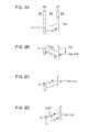
- FIGS. 1A and 1B illustrate an exemplary configuration of a photoelectric converter.
- FIGS. 2A to 2D illustrate an exemplary operation of a photoelectric converter.
- FIG. 3 illustrates an exemplary operation of a photoelectric converter.
- FIG. 4 is a bird's-eye view of an exemplary photoelectric converter.
- FIG. 5 is a cross-sectional view of an exemplary photoelectric converter taken along line V-V of FIG. 4 .
- FIG. 6 illustrates an exemplary configuration of a photoelectric conversion system.
- FIGS. 1A and 1B illustrate an exemplary configuration of a photoelectric converter of the present embodiment.
- a photoelectric converter 10 illustrated in FIG. 1A includes a pixel 1000 , a capacitance driving unit 12 , a vertical signal line 17 , a current source 18 , and a column signal processor 20 .
- the photoelectric converter 10 includes a power supply unit 30 a.
- the pixel 1000 includes a reset unit 14 and a pixel output unit 16 .
- FIG. 1A A single pixel 1000 is illustrated in FIG. 1A , which is one of a plurality of pixels 1000 arranged in a plurality of rows and columns.
- FIG. 1A illustrates a single vertical signal line 17 , a single current source 18 , and a single column signal processor 20 . These are one of a plurality of columns of vertical signal lines 17 , current sources 18 , and column signal processors 20 provided corresponding to each column in which a plurality of pixels 1000 are arranged.
- a photoelectric conversion unit 101 a include a common electrode 201 , a blocking layer 203 , a photoelectric conversion layer 205 , an insulating layer 207 , and a pixel electrode 209 .
- the common electrode 201 is electrically connected to a plurality of photoelectric conversion units 101 a in common.
- the common electrode 201 supplies a potential to a plurality of photoelectric conversion units 101 a in common.
- the blocking layer 203 is provided between the common electrode 201 and the photoelectric conversion layer 205 .
- the photoelectric conversion layer 205 is provided between the blocking layer 203 and the insulating layer 207 .
- the insulating layer 207 is provided between the photoelectric conversion layer 205 and the pixel electrode 209 .
- the common electrode 201 is formed by a conductive member with high transmittance of light of a wavelength region in which the photoelectric conversion layer 205 has sensitivity.
- a compound including indium, such as indium tin oxide (ITO), and/or tin, and a compound, such as ZnO, are used as a material of the common electrode 201 . Therefore, the photoelectric conversion layer 205 of the present embodiment may take in a greater amount of light than in a configuration in which an opaque electrode, such as copper, is used as the common electrode 201 .
- the common electrode 201 of the present embodiment may be formed by polysilicon or metal of which thinness allows a certain amount of light to pass through.
- the blocking layer 203 reduces injection of charge of the same conductivity type as that of signal charge accumulated by the photoelectric conversion layer 205 in the photoelectric conversion layer 205 from the common electrode 201 .
- the photoelectric conversion layer 205 is depleted due to a potential difference between a potential Vs applied to the common electrode 201 and a potential of the pixel electrode 209 .
- An inclination of the potential of the photoelectric conversion layer 205 is reversed depending on a relationship between the potential Vs applied to the common electrode 201 and the potential of the pixel electrode 209 . With this configuration, the photoelectric conversion layer 205 may accumulate signal charge and discharge the accumulated signal charge. An operation of the photoelectric conversion unit 101 a is described later.
- a power supply voltage supplied to the common electrode 201 is a potential Vs supplied from the power supply unit 30 a.
- the photoelectric conversion layer 205 is formed by, for example, intrinsic amorphous silicon (hereafter, a-Si), low-concentration P-type a-Si, and low-concentration N-type a-Si.
- the photoelectric conversion layer 205 may be formed by a compound semiconductor.
- the compound semiconductor may include III-V compound semiconductors, such as BN, GaAs, GaP, AlSb, and GaAlAsP, II-VI compound semiconductors, such as CdSe, ZnS, and HdTe, and IV-VI compound semiconductors, such as PbS, PbTe, and CuO.
- the photoelectric conversion layer 205 may be formed by an organic material.
- fullerene, coumarin 6 (C 6 ), Rhodamine 6G (R6G), zinc phthalocyanine (ZnPc), quinacridone, a phthalocyanine-based compound, and a naphthalocyanine-based compound may be used.
- the photoelectric conversion layer 205 may use a quantum dot film including above-described compound semiconductor.
- the photoelectric conversion layer 205 is formed by a semiconductor, impurity concentration of the semiconductors is desirably low, or the semiconductors are desirably intrinsic.
- a depletion layer may be expanded sufficiently in the photoelectric conversion layer 205 , which provides effects, such as increased sensitivity and reduced noise.
- the blocking layer 203 is formed by the same material as that of the semiconductors used for the photoelectric conversion layer 205 , and the N-type or P-type semiconductors with higher impurity concentration than that of the semiconductors used in the photoelectric conversion layer 205 .
- the photoelectric conversion layer 205 N-type a-Si with impurities doped in the blocking layer 203 , or P-type a-Si with impurities doped are used. Since the Fermi level varies depending on the impurity concentration, the blocking layer 203 functions as a potential barrier for either one of the electron or hole.
- the photoelectric conversion layer 205 includes a quantum dot film
- a blocking layer 203 formed by the same material as that of the semiconductor used in the quantum dot film and of a conductivity type opposite to the conductivity type of the quantum dot film may be provided.
- the quantum dot film is P-type PbS
- the blocking layer 203 may be N-type PbS. If the blocking layer 203 is formed by the same material and of the same conductivity type as that of the quantum dot film, the quantum dot film and the blocking layer 203 may be different in impurity concentration.
- the blocking layer 203 may be formed by a material different from that of the photoelectric conversion layer 205 .
- a hetero-junction is formed. Since a band gap varies depending on the material, a potential barrier may be formed in either of the electron or the hole.
- the photoelectric conversion layer 205 includes a quantum dot film, for example, PbS may be used as the quantum dot film, and ZnO may be used as the blocking layer 203 .
- the insulating layer 207 is disposed between the photoelectric conversion layer 205 and the pixel electrode 209 .
- the insulating layer 207 may be formed by, for example, amorphous silicon oxide (hereafter, a-SiO), amorphous silicon nitride (a-SiN), and an organic material.
- the thickness of the insulating layer 207 may be defined so that the signal charge does not pass through the insulating layer 207 by the tunnel effect. This configuration may reduce current leakage, and thereby reduce noise.
- the thickness of the insulating layer 207 is desirably 50 nm or more.
- a hydrogen treatment may be performed to terminate the dangling bond with hydrogen. With this configuration, noise may be reduced.
- the pixel electrode 209 is formed by a conductive member, such as metal.
- the pixel electrode 209 is formed by a conductive member constituting wiring, or the same conductive member constituting a pad electrode for connecting to the outside.
- the thus configured photoelectric conversion unit 101 a of the present embodiment may form the pixel electrode 209 and the conductive member constituting wiring or the pad electrode at the same time. Therefore, the photoelectric conversion unit 101 a of the present embodiment may be produced in a more simplified process than in a case in which the pixel electrode 209 is formed by a material different from the conductive member constituting wiring, or the pad electrode.
- the pixel electrode 209 Since the pixel electrode 209 is formed by metal, the pixel electrode 209 may cause the light passed through the photoelectric conversion layer 205 and reached the pixel electrode 209 to be reflected on the photoelectric conversion layer 205 . Thus, light quantity received by the photoelectric conversion layer 205 becomes greater than in a case in which the pixel electrode 209 is formed by other materials than metal, such as an oxide conductive film. Therefore, sensitivity of photoelectric conversion unit 101 a is increased.
- the common electrode 201 of the photoelectric conversion unit 101 a is electrically connected to the power supply unit 30 a .
- the power supply unit 30 a supplies the potential Vs to the common electrode 201 .
- the reset unit 14 includes a reset transistor 14 a .
- a reset potential Vres is supplied to one of a source and a drain, and the other of the source and the drain is electrically connected to a node FD.
- the reset potential Vres is a potential lower than the potential Vs.
- the potential Vs is set to 5V and the reset potential Vres is set to 2V.
- a signal ⁇ RES is input in a gate of the reset transistor 14 a from an unillustrated vertical scanning circuit.
- the capacitance driving unit 12 includes a buffer circuit 12 a and a capacitive element 12 b .
- a first node which is one of the nodes of the capacitive element 12 b , is electrically connected to the node FD, which is a third node.
- the first node of the capacitive element 12 b is electrically connected to the pixel electrode 209 of the photoelectric conversion unit 101 a .
- a second node, which is the other node of the capacitive element 12 b is electrically connected to the buffer circuit 12 a .
- a signal ⁇ Vp is input from an unillustrated timing generator.
- the buffer circuit 12 a supplies, to the capacitive element 12 b , a potential that is a buffered potential of the signal ⁇ Vp.
- the timing generator is a capacitance potential supply unit that supplies the signals ⁇ Vp of different potentials to the capacitive element 12 b via the buffer circuit 12 a.
- the capacitive element 12 b is electrically connected to the node FD.
- the capacitive element 12 b includes, for example, mutually facing two electrodes.
- the two electrodes are formed by, for example, polysilicon and metal.
- the capacitive element 12 b includes a semiconductor region, and a gate electrode disposed above the semiconductor region.
- noise may be reduced during the readout of optical signals from the photoelectric conversion unit 101 a . This noise reduction effect is described.
- the potential of the node FD is controlled.
- the potential of the pixel electrode 209 of the photoelectric conversion unit 101 a varies depending on the ratio between the capacitive element 12 b , and synthetic capacity of gate capacity of an amplifying transistor 16 a connected via the node FD and a capacitance value of the capacity component between the common electrode 201 and the pixel electrode 209 (hereafter, considered to be a capacitance value of the photoelectric conversion unit 101 a ). This is because the capacitive element 12 b and the synthetic capacity may be regarded as two capacitance connected in series.
- the capacitive element 12 b is electrically connected to the node FD.
- the node in which the potential of the signal ⁇ Vp of the capacitive element 12 b is input and the node FD are separated electrically.
- the capacitive element 12 b is electrically connected to the node FD. Therefore, when the potential of the pixel electrode 209 is controlled to read the optical signal from the photoelectric conversion unit 101 a , a large potential difference may be applied to between the common electrode 201 and the pixel electrode 209 . Therefore, since the photoelectric conversion layer 205 may be depleted easily in the photoelectric converter of the present embodiment, noise included in the optical signal may be reduced.
- the pixel output unit 16 includes the amplifying transistor 16 a and a selection transistor 16 b .
- a gate which is an input node of the amplifying transistor 16 a , is electrically connected to the node FD.
- a potential Vdd is input in one of a source and a drain of the amplifying transistor 16 a , and the other of the source and the drain is electrically connected to one of a source and a drain of the selection transistor 16 b .
- the other of the source and the drain of the selection transistor 16 b is electrically connected to the vertical signal line 17 .
- a signal ⁇ Sel is input in a gate of the selection transistor 16 b from an unillustrated vertical scanning circuit.
- the amplifying transistor 16 a which is an amplifier unit, outputs a signal that is an amplified signal of the signal output from the pixel electrode 209 .
- a node of the selection transistor 16 b connected to the vertical signal line 17 is an output node of the amplifier unit.
- the current source 18 is electrically connected to the selection transistor 16 b via the vertical signal line 17 .
- a source follower circuit is configured by the amplifying transistor 16 a and the current source 18 .
- the signal output to the vertical signal line 17 via the selection transistor 16 b from the amplifying transistor 16 a is input in the column signal processor 20 .
- the column signal processor 20 outputs a signal based on the signal output to the vertical signal line 17 from the amplifying transistor 16 a.
- FIG. 1B illustrates a configuration of the column signal processor 20 .
- the column signal processor 20 includes a column amplifier unit 21 and an AD conversion unit 22 .
- the column amplifier unit 21 includes a capacitive element C 0 , a capacitive element C 1 , a switch SW 1 , and an amplifier 23 .
- An operation of the switch SW 1 is controlled by a signal ⁇ C 0 output from an unillustrated timing generator.
- a signal output to the vertical signal line 17 from the amplifying transistor 16 a is input in an inverting input node of the amplifier 23 via the capacitive element C 0 .
- a reference voltage Vref is input in a non-inverting input node of the amplifier 23 .
- a signal Vamp output from the amplifier 23 is an inverted and amplified signal of the signal input in the inverting input node of the amplifier 23 .
- An amplification factor of the amplifier 23 is k of a negative value.
- the AD conversion unit 22 includes a comparator 25 and memory 27 .
- the signal Vamp is input in the comparator 25 from the amplifier 23 .
- the comparator 25 compares a potential of a ramp signal Ramp input from the outside of the column signal processor 20 and a potential of the signal Vamp.
- the ramp signal Ramp is a signal of which potential changes monotonously with time.
- the signal that the comparator 25 outputs to the memory 27 is the signal indicating a comparison result between the potential of the ramp signal Ramp and the potential of the signal Vamp.
- the memory 27 holds a signal indicating a calculation result of time from the timing at which the ramp signal Ramp starts the change of potential until the signal level of the comparison result signal has changed.
- the signal which the memory 27 holds is a digital signal based on the signal Vamp.
- the digital signal that the memory 27 of each of a plurality of columns of column signal processors 20 holds is sequentially output outside of the photoelectric converter by an unillustrated horizontal scanning circuit for each column.
- FIGS. 2A to 2D each schematically illustrate an energy band in the photoelectric conversion unit 101 a .
- FIGS. 2A to 2D each illustrate the common electrode 201 , the blocking layer 203 , the photoelectric conversion layer 205 , the insulating layer 207 , and the pixel electrode 209 .
- a vertical axis in each of FIGS. 2A to 2D indicates a potential to electrons. The potential to electrons becomes higher at higher positions in FIGS. 2A to 2D . The potential becomes lower at lower positions in FIGS. 2A to 2D .
- the common electrode 201 and the pixel electrode 209 the Fermi level is illustrated.
- a band gap between an energy level of a conducting zone and an energy level of a valence band is illustrated.
- the following steps (1) to (5) are performed repeatedly. (1) Resetting the input node of the amplifier unit, (2) Reading the noise signal, (3) Transmitting the signal charge from the photoelectric conversion unit, (4) Reading the optical signal, and (5) Accumulating the signal charge. Each step is described below.
- FIG. 2A illustrates a state of the photoelectric conversion unit 101 a from step (1) to step (2).
- the potential Vs is supplied to the common electrode 201 .
- a first potential Vs is, for example, 3V. Holes illustrated by white circles are accumulated in the photoelectric conversion layer 205 as the signal charge produced during an exposure period.
- a surface potential of the photoelectric conversion layer 205 on the side of the insulating layer 207 varies depending on the amount of the accumulated holes.
- the buffer circuit 12 a supplies the first potential Vd 1 to the capacitive element 12 b .
- the first potential Vd 1 is, for example, 0V.
- the reset transistor 14 a is turned on in this state.
- the node including the pixel electrode 209 i.e., the potential of the node FD
- the reset potential Vres is, for example, 1V.
- the node FD is connected to a gate which is the input node of the amplifying transistor 16 a .
- the input node of the amplifier unit is reset.
- the reset transistor 14 a is turned off, and the node FD becomes electrically floating. At this time, reset noise by the reset transistor 14 a may occur. The holes of the signal charge are still accumulated in the photoelectric conversion layer 205 .
- the amplifying transistor 16 a When the selection transistor 16 b is turned on, the amplifying transistor 16 a outputs the noise signal including the reset noise.
- FIGS. 2B and 2C illustrate states of the photoelectric conversion unit 101 a in step (3).
- the buffer circuit 12 a supplies a second potential Vd 2 to the capacitive element 12 b . Since the holes are used as the signal charge, the second potential Vd 2 is higher than the first potential Vd 1 .
- the second potential Vd 2 is, for example, 5V.
- dVB ( Vd 2 ⁇ Vd 1) ⁇ C 1/( C 1+ C 2) (1).
- dVB ( Vd 2 ⁇ Vd 1) ⁇ (1/2) (2).
- the changing quantity dVB of the potential of the pixel electrode 209 is sufficiently larger than a difference between the potential Vs of the common electrode 201 and the reset potential Vres (Vs ⁇ Vres). Therefore, the potential of the pixel electrode 209 becomes lower than the potential of the common electrode 201 , and an inclination of the potential of the photoelectric conversion layer 205 is inverted.
- electrons illustrated by black circles are injected into the photoelectric conversion layer 205 from the first electrode 201 .
- a part or all of the holes accumulated in the photoelectric conversion layer 205 as the signal charge move toward the blocking layer 203 .
- the moved holes are recombined with majority carriers of the blocking layer 203 and disappear.
- the holes of the photoelectric conversion layer 205 are discharged from the photoelectric conversion layer 205 . If the entire photoelectric conversion layer 205 is depleted, all the holes accumulated as the signal charge are discharged.
- the buffer circuit 12 a supplies the first potential Vd 1 to the capacitive element 12 b .
- the inclination of the potential of the photoelectric conversion layer 205 is inverted again.
- the electrons injected into the photoelectric conversion layer 205 in the state of FIG. 2B are discharged from the photoelectric conversion layer 205 .
- Injection of the holes from the common electrode 201 into the photoelectric conversion layer 205 is reduced by the blocking layer 203 . Therefore, the potential of the node FD changes from the reset state to a state by a potential Vsig in accordance with the amount of the holes disappeared. That is, the potential Vsig in accordance with the amount of the holes accumulated as the signal charge appears in the node FD.
- the potential Vsig in accordance with the amount of the accumulated holes is referred to as an optical signal component.
- the selection transistor 16 b is turned on in the state illustrated in FIG. 2C . Then, the amplifying transistor 16 a outputs the optical signal.
- a difference between the noise signal read in step (2) and the optical signal read in step (4) is the signal based on the potential Vsig in accordance with the accumulated signal charge.
- FIG. 2D illustrates the state of the photoelectric conversion unit 101 a in step (5).
- the potential Vs is supplied to the common electrode 201 , and the reset potential Vres is supplied to the node FD. Since the reset potential Vres is lower than the potential Vs of the common electrode 201 , the electrons of the photoelectric conversion layer 205 are discharged to the common electrode 201 .
- the holes of the photoelectric conversion layer 205 move toward an interface between the photoelectric conversion layer 205 and the insulating layer 207 . However, since the holes cannot move to the insulating layer 207 , the holes are accumulated in the photoelectric conversion layer 205 .
- the blocking layer 203 reduces injection of the holes into the photoelectric conversion layer 205 .
- a potential Vch is a potential to which the pixel electrode 209 changes in accordance with the holes accumulated in the photoelectric conversion layer 205 .
- the second potential Vd 2 may be lower than the first potential Vd 1 .
- the conductivity type of the blocking layer 203 may be opposite to that of the blocking layer 203 of the present embodiment. Therefore, the inclinations of the potential in FIGS. 2A to 2D are inverted. Other operations are the same.
- FIG. 3 illustrates an operation of the photoelectric converter illustrated in FIG. 1A .
- the reset transistor 14 a and the selection transistor 16 b illustrated in FIG. 1A are, in this order, turned on when the signal ⁇ Res and the signal ⁇ Sel are at Hi levels (hereafter, “Hi”), and turned off when these signals are at Lo levels (hereafter, “Lo”).
- the period T 1 is a reset period of the node FD
- the period T 2 is a period in which the node FD is in a floating state
- the period T 3 is a refreshment period of the photoelectric conversion unit 101 a
- the period T 4 is a signal charge holding period of the node FD.
- the amplifying transistor 16 a does not operate during the period from time t 3 to time t 4 .
- the photoelectric conversion unit 101 a starts a new photoelectric conversion event at the period T 4 after the refreshment.
- VFD the potential of the node FD
- Vline the potential of the vertical signal line 17
- the photoelectric conversion unit 101 a Before time t 1 , the photoelectric conversion unit 101 a is accumulating the signal charge.
- an unillustrated vertical scanning circuit switches the signal level of the signal ⁇ Res from Lo to Hi. Then, the reset transistor 14 a is turned on and the pixel electrode 209 and the node FD are reset to potential Vres.
- the vertical scanning circuit switches the signal ⁇ Sel from Lo to Hi. Then, the selection switch 16 is turned on. Since a current is supplied to the amplifying transistor 16 a from the current source 18 , the amplifying transistor 16 a becomes in an operating state.
- an unillustrated timing generator switches the signal level of the signal ⁇ C 0 to Hi. Then, the charge of the capacitive element C 1 is reset.
- the vertical scanning circuit switches the signal level of the signal ⁇ Res to Lo. Then, the node FD becomes floating.
- the floating potential V 21 of the node FD at this time is referred to as a reset FD potential.
- the amplifying transistor 16 a outputs a signal based on the reset FD potential to the vertical signal line 17 .
- the operation during the period T 1 from time t 1 to time t 2 is the operation corresponding to step (2) described above.
- the timing generator switches the signal level of the signal ⁇ C 0 to Lo at subsequent time t 21 . Then, the capacitive element C 0 holds the signal output by the amplifying transistor 16 a to the vertical signal line 17 and based on the reset FD potential.
- the signal Vamp at time t 22 mainly includes an offset component that the column amplifier unit 21 has. This signal is referred to as an offset signal.
- the ramp signal Ramp changes the potential depending on time during the period from time t 22 until time t 23 .
- the period from time t 22 until time t 23 is the period in which the AD conversion unit 22 converts the offset signal into the digital signal. This period is denoted by N-AD in FIG. 3 .
- the digital signal based on the offset signal that the AD conversion unit 22 obtained is referred to as a digital N signal.
- an unillustrated timing generator switches the signal level of the signal ⁇ Vp from Lo to the potential Vp 1 , which is the signal level of Hi.
- the potential Vp 1 is 10V and the signal level of the signal ⁇ Vp of Lo is 0V.
- the timing generator switches the signal ⁇ Vp to Lo at subsequent time t 32 .
- the optical signal is output to the pixel electrode 209 .
- the node FD has a potential based on the optical signal. This operation corresponds to the step (3) described above.
- FIG. 3 illustrates a case where light has not substantially entered the photoelectric conversion unit 101 a .
- the potential of the node FD is illustrated as the reset FD potential, the potential of the node FD at time t 32 is the potential based on the optical signal.
- the amplifying transistor 16 a outputs the signal based on the optical signal to the vertical signal line 17 .
- This operation corresponds to step (4) described above.
- the signal Vamp of the column amplifier unit 21 has the potential of the signal that is an amplified signal based on the optical signal output from the amplifying transistor 16 a (hereafter, “amplified optical signal).
- the ramp signal Ramp changes the potential depending on the time during the period from time t 41 until time t 42 .
- the period from time t 41 until time t 42 is the period in which the AD conversion unit 22 converts the amplified optical signal into the digital signal. This period is denoted by S-AD in FIG. 3 .
- the digital signal based on the amplified optical signal that the AD conversion unit 22 obtained is referred to as a digital S signal.
- the memory 27 of each column holds the digital N signal and the digital S signal.
- An unillustrated horizontal scanning circuit sequentially reads the digital N signal and the digital S signal from the memory 27 of each column, and outputs outside the photoelectric converter.
- FIG. 4 is a bird's-eye view of the photoelectric converter of the present embodiment.
- FIG. 5 is a schematic sectional view along line V-V of FIG. 4 .
- the pixels 1000 are arranged in a matrix form in the pixel unit 1 .
- the common electrode 201 is electrically connected via a through hole (not illustrated) to a reference voltage line 109 disposed on the semiconductor substrate 100 .
- the reference voltage line 109 is formed by metal wiring.
- the common electrode 201 is desirably formed to at least cover the pixel unit 1 and the reference voltage line 109 .
- the reference voltage lines 109 may be disposed at four sides of the periphery of the pixel unit 1 . In this case, each of a plurality of reference voltage lines 109 provided at each side on the periphery of the pixel unit 1 may be electrically connected to the common electrode 201 via a via plug.
- the photoelectric converter includes a voltage supply terminal 2 .
- the voltage supply terminal 2 is electrically connected to the outside of the photoelectric converter, and to the reference voltage line 109 .
- a predetermined voltage is supplied to the voltage supply terminal 2 from the outside of the photoelectric converter.
- a transistor M 3 is provided in the semiconductor substrate 100 .
- One of main nodes of the transistor M 3 is electrically connected to the pixel electrode 209 via a wiring layer.
- the insulating layer 207 is provided in the pixel electrode 209 on the incident surface side thereof.
- the photoelectric conversion layer 205 and the blocking layer 203 are provided in this order on the insulating layer 207 .
- the common electrode 201 is provided in the blocking layer 203 on the incident surface side thereof.
- the reference voltage line 109 formed by metal wiring is provided in the peripheral region of the pixel unit 1 .
- the peripheral region of the pixel unit 1 refers to a region located outside the entire periphery of a plurality of pixels 1000 included in the pixel unit 1 .
- the reference voltage line 109 is electrically connected to the connecting electrode 107 via the through hole 108 .
- An oxide conductive film 106 is provided between the connecting electrode 107 and the common electrode 201 .
- the connecting electrode 107 is a second electrode which supplies, to the common electrode 201 , a potential that the common electrode 201 supplies to a plurality of photoelectric conversion units 101 a.
- the oxide conductive film 106 may be formed, for example, by indium tin oxide (ITO) and indium zinc oxide (IZO).
- the oxide conductive film 106 may be a film containing indium oxide.
- the oxide conductive film 106 may also be a film containing ZnO.
- An current flowing path is comprised by the common electrode 201 , the connecting electrode 107 , and the oxide conductive film 106 .
- a transistor M 3 is formed in the semiconductor substrate 100 . Then, the reference voltage line 109 is formed on the periphery of the pixel unit 1 . The through hole 108 is formed. The connecting electrode 107 is formed. The pixel electrode 209 is formed in parallel to the formed connecting electrode 107 . The connecting electrode 107 and the pixel electrode 209 may be formed at the same time.
- the semiconductor substrate 100 is washed to remove particles of the pixel electrode 209 and the connecting electrode 107 .
- the semiconductor substrate 100 is washed by two fluid washing with water.
- a natural oxide film is formed on a metal surface by oxygen remaining in the washing water and oxygen in clean air of a clean room.
- the formed natural oxide film is removed before the next process of forming the oxide conductive film 106 .
- the natural oxide film may be removed by plasma etching or etching using a medical fluid.
- the oxide conductive film 106 is formed on the connecting electrode 107 .
- the insulating layer 207 , the photoelectric conversion layer 205 , and the blocking layer 203 are formed on the pixel electrode 209 .
- the insulating layer 207 , the photoelectric conversion layer 205 , and the blocking layer 203 are formed also on the oxide conductive film 106 .
- a region above the oxide conductive film 106 is patterned to remove the insulating layer 207 , the photoelectric conversion layer 205 , and the blocking layer 203 . A resist used for the patterning is also removed.
- a surface of the blocking layer 203 and a surface of the oxide conductive film 106 of the connecting electrode 107 are washed to remove particles therefrom.
- the semiconductor substrate 100 is washed by two fluid washing with water.
- An insulating natural oxide film is formed on a metal surface during the washing. Therefore, in a configuration in which the connecting electrode 107 and the common electrode 201 are connected directly not via the oxide conductive film 106 , the natural oxide film formed on the surface of the connecting electrode 107 increases electric resistance between the connecting electrode 107 and the common electrode 201 . Removal of the natural oxide film is difficult because it can cause damage to the photoelectric conversion unit 101 a.
- the oxide conductive film 106 is provided on the connecting electrode 107 .
- An insulating natural oxide film is less easily formed on the oxide conductive film 106 during this washing process as compared with the metal surface. Therefore, as compared with a configuration in which the connecting electrode 107 and the common electrode 201 are connected directly not via the oxide conductive film 106 , the photoelectric converter of the present embodiment is capable of reducing a decrease in conductivity between the connecting electrode 107 and the common electrode 201 caused during the washing process.
- the common electrode 201 is formed to extend from above the blocking layer 203 of the photoelectric conversion unit 101 a to above the oxide conductive film 106 .
- the oxide conductive film 106 is provided between the connecting electrode 107 and the common electrode 201 .
- an insulating natural oxide film is less easily formed on the surface of the connecting electrode 107 . Therefore, a decrease in conductivity between the connecting electrode 107 and the common electrode 201 may be reduced.
- the reference voltage lines 109 are disposed at four sides on the periphery of the pixel unit 1 , and are electrically connected to the common electrode 201 via the through hole 108 in each side.
- the present disclosure is not limited to these configurations.
- the reference voltage line 109 may be disposed at one side or at two opposite sides of the periphery of the pixel unit 1 .
- the metal wiring of the photoelectric converter of the present embodiment may be a multilayer wiring structure instead of a single-layer wiring structure, such as aluminum (Al).
- a configuration of TiN/Al/TiN using barrier metal may be employed.
- the barrier metal prevents diffusion of the metallic material and increases adhesiveness to a Si substrate.
- Metals other than Al, e.g., Cu, may be used for the metal wiring.
- the potential of the common electrode 201 is defined as the predetermined potential, and the charge of the photoelectric conversion unit 101 a is refreshed by changing the potential of the pixel electrode 209 .
- the potential of the pixel electrode 209 is defined as a predetermined potential, and the charge of the photoelectric conversion unit 101 a may be refreshed by changing the potential of the common electrode 201 .
- FIG. 6 is a schematic diagram of a photoelectric conversion system in which the photoelectric converter of the first embodiment is applied to a digital still camera as an example of the photoelectric conversion system.
- the photoelectric conversion system illustrated to FIG. 6 includes a photoelectric converter 154 , a barrier 151 for the protection of a lens, a lens 152 that focuses an optical image of an object on the photoelectric converter 154 , and a diaphragm 153 that makes light quantity passing through the lens 152 variable.
- the lens 152 and the diaphragm 153 are an optical system that condenses light to the photoelectric converter 154 .
- the photoelectric conversion system illustrated in FIG. 6 further includes an output signal processor 155 that processes an output signal output from the photoelectric converter 154 .
- the output signal processor 155 performs AD conversion of converting analog signals output from the photoelectric converter 154 into digital signals.
- the output signal processor 155 outputs image data after, as necessity, performing various corrections and compressions.
- the photoelectric conversion system illustrated in FIG. 6 further includes a buffer memory unit 156 that temporarily stores image data, and an external interface unit (external I/F unit) 157 for the communication with, for example, an external computer.
- the photoelectric conversion system further includes a recording medium 159 , such as semiconductor memory, for recording or reading of picked image data, and a recording medium control interface unit (recording medium I/F unit) 158 for recording on or reading from recording medium 159 .
- the recording medium 159 may be integrated in or may be detached from the photoelectric conversion system.
- the photoelectric conversion system further includes a comprehensive control/calculation unit 1510 that controls various calculations and the entire digital still camera, and a timing generation unit 1511 that outputs various timing signals to the photoelectric converter 154 and the output signal processor 155 .
- the timing signals or other signals may be input from the outside, and it is only necessary that the photoelectric conversion system at least includes the photoelectric converter 154 , and the output signal processor 155 that processes the output signal output from the photoelectric converter 154 .
- the photoelectric conversion system of the present embodiment is capable of performing an image pickup operation with the photoelectric converter 154 applied thereto.
- the present disclosure provides a photoelectric converter, and a photoelectric conversion system, capable of reducing a decrease in conductivity between the connecting electrode and the common electrode.
Landscapes
- Solid State Image Pick-Up Elements (AREA)
- Light Receiving Elements (AREA)
Applications Claiming Priority (2)
| Application Number | Priority Date | Filing Date | Title |
|---|---|---|---|
| JP2014183698A JP6465597B2 (ja) | 2014-09-09 | 2014-09-09 | 光電変換装置、光電変換システム |
| JP2014-183698 | 2014-09-09 |
Publications (2)
| Publication Number | Publication Date |
|---|---|
| US20160071986A1 US20160071986A1 (en) | 2016-03-10 |
| US9698189B2 true US9698189B2 (en) | 2017-07-04 |
Family
ID=55438295
Family Applications (1)
| Application Number | Title | Priority Date | Filing Date |
|---|---|---|---|
| US14/846,332 Expired - Fee Related US9698189B2 (en) | 2014-09-09 | 2015-09-04 | Photoelectric converter and photoelectric conversion system |
Country Status (2)
| Country | Link |
|---|---|
| US (1) | US9698189B2 (enExample) |
| JP (1) | JP6465597B2 (enExample) |
Families Citing this family (4)
| Publication number | Priority date | Publication date | Assignee | Title |
|---|---|---|---|---|
| CN119789558A (zh) * | 2018-06-14 | 2025-04-08 | 松下知识产权经营株式会社 | 具备控制电极、透明电极和连接层的图像传感器 |
| TWI831995B (zh) * | 2019-10-04 | 2024-02-11 | 日商索尼半導體解決方案公司 | 固體攝像元件及電子機器 |
| JP7527806B2 (ja) * | 2020-02-19 | 2024-08-05 | キヤノン株式会社 | 光電変換装置、撮像システム、移動体 |
| TW202437550A (zh) * | 2023-03-07 | 2024-09-16 | 睿生光電股份有限公司 | 偵測裝置 |
Citations (3)
| Publication number | Priority date | Publication date | Assignee | Title |
|---|---|---|---|---|
| JP2007059516A (ja) | 2005-08-23 | 2007-03-08 | Fujifilm Corp | 光電変換素子、撮像素子、および該光電変換素子の製造方法 |
| JP2011029337A (ja) | 2009-07-23 | 2011-02-10 | Sony Corp | 固体撮像装置とその製造方法、及び電子機器 |
| JP2012124343A (ja) | 2010-12-08 | 2012-06-28 | Fujifilm Corp | 撮像素子及び撮像素子の製造方法 |
Family Cites Families (8)
| Publication number | Priority date | Publication date | Assignee | Title |
|---|---|---|---|---|
| JP4224661B2 (ja) * | 2000-02-10 | 2009-02-18 | エルジー ディスプレイ カンパニー リミテッド | 銅配線基板及びその製造方法並びに液晶表示装置 |
| JP2006049873A (ja) * | 2004-07-06 | 2006-02-16 | Fuji Photo Film Co Ltd | 機能素子 |
| JP4705062B2 (ja) * | 2007-03-01 | 2011-06-22 | 株式会社神戸製鋼所 | 配線構造およびその作製方法 |
| JP2008227092A (ja) * | 2007-03-12 | 2008-09-25 | Fujifilm Corp | 光電変換素子、撮像素子、撮像装置 |
| JP5536488B2 (ja) * | 2010-02-22 | 2014-07-02 | ローム株式会社 | カラー用固体撮像装置 |
| JP2011238781A (ja) * | 2010-05-11 | 2011-11-24 | Panasonic Corp | 固体撮像素子及びその製造方法 |
| JP2012074418A (ja) * | 2010-09-27 | 2012-04-12 | Fujifilm Corp | 固体撮像素子及び撮像装置 |
| WO2014103150A1 (ja) * | 2012-12-28 | 2014-07-03 | パナソニック株式会社 | 固体撮像装置およびその製造方法 |
-
2014
- 2014-09-09 JP JP2014183698A patent/JP6465597B2/ja not_active Expired - Fee Related
-
2015
- 2015-09-04 US US14/846,332 patent/US9698189B2/en not_active Expired - Fee Related
Patent Citations (3)
| Publication number | Priority date | Publication date | Assignee | Title |
|---|---|---|---|---|
| JP2007059516A (ja) | 2005-08-23 | 2007-03-08 | Fujifilm Corp | 光電変換素子、撮像素子、および該光電変換素子の製造方法 |
| JP2011029337A (ja) | 2009-07-23 | 2011-02-10 | Sony Corp | 固体撮像装置とその製造方法、及び電子機器 |
| JP2012124343A (ja) | 2010-12-08 | 2012-06-28 | Fujifilm Corp | 撮像素子及び撮像素子の製造方法 |
Also Published As
| Publication number | Publication date |
|---|---|
| US20160071986A1 (en) | 2016-03-10 |
| JP6465597B2 (ja) | 2019-02-06 |
| JP2016058555A (ja) | 2016-04-21 |
Similar Documents
| Publication | Publication Date | Title |
|---|---|---|
| US9722107B2 (en) | Photoelectric conversion device and imaging system | |
| US9826181B2 (en) | Photoelectric conversion device and imaging system | |
| US9515106B2 (en) | Radiation imaging device with metal-insulator-semiconductor photodetector and thin film transistor | |
| US10446594B2 (en) | Image pickup device and image pickup system | |
| US10547016B2 (en) | Photoelectric conversion apparatus and imaging system | |
| US9941315B2 (en) | Photoelectric conversion device and imaging system | |
| US10244193B2 (en) | Imaging apparatus and imaging system | |
| CN105323510B (zh) | 光电变换装置、光电变换系统和光电变换装置的驱动方法 | |
| US9698189B2 (en) | Photoelectric converter and photoelectric conversion system | |
| US9866774B2 (en) | Photoelectric conversion device and imaging system | |
| JP7027175B2 (ja) | 半導体装置および機器 | |
| US10091444B2 (en) | Photoelectric conversion apparatus and photoelectric conversion system | |
| JP2017098815A (ja) | 光電変換装置、および、撮像システム | |
| JP2017103429A (ja) | 撮像装置、および、撮像システム | |
| JP6703053B2 (ja) | 光電変換装置、光電変換システム |
Legal Events
| Date | Code | Title | Description |
|---|---|---|---|
| AS | Assignment |
Owner name: CANON KABUSHIKI KAISHA, JAPAN Free format text: ASSIGNMENT OF ASSIGNORS INTEREST;ASSIGNOR:YAMASHITA, TAKANORI;REEL/FRAME:037162/0051 Effective date: 20150820 |
|
| STCF | Information on status: patent grant |
Free format text: PATENTED CASE |
|
| FEPP | Fee payment procedure |
Free format text: MAINTENANCE FEE REMINDER MAILED (ORIGINAL EVENT CODE: REM.); ENTITY STATUS OF PATENT OWNER: LARGE ENTITY |
|
| LAPS | Lapse for failure to pay maintenance fees |
Free format text: PATENT EXPIRED FOR FAILURE TO PAY MAINTENANCE FEES (ORIGINAL EVENT CODE: EXP.); ENTITY STATUS OF PATENT OWNER: LARGE ENTITY |
|
| STCH | Information on status: patent discontinuation |
Free format text: PATENT EXPIRED DUE TO NONPAYMENT OF MAINTENANCE FEES UNDER 37 CFR 1.362 |
|
| FP | Lapsed due to failure to pay maintenance fee |
Effective date: 20210704 |