US9646915B2 - Heat dissipation device and semiconductor device - Google Patents
Heat dissipation device and semiconductor device Download PDFInfo
- Publication number
- US9646915B2 US9646915B2 US14/414,728 US201314414728A US9646915B2 US 9646915 B2 US9646915 B2 US 9646915B2 US 201314414728 A US201314414728 A US 201314414728A US 9646915 B2 US9646915 B2 US 9646915B2
- Authority
- US
- United States
- Prior art keywords
- passage
- coolant
- hole
- heat dissipation
- dissipation device
- Prior art date
- Legal status (The legal status is an assumption and is not a legal conclusion. Google has not performed a legal analysis and makes no representation as to the accuracy of the status listed.)
- Expired - Fee Related, expires
Links
- 230000017525 heat dissipation Effects 0.000 title claims description 89
- 239000004065 semiconductor Substances 0.000 title claims description 76
- 239000000919 ceramic Substances 0.000 claims abstract description 174
- 239000002826 coolant Substances 0.000 claims description 273
- 229910052751 metal Inorganic materials 0.000 claims description 39
- 239000002184 metal Substances 0.000 claims description 39
- 238000001816 cooling Methods 0.000 claims description 37
- 230000015572 biosynthetic process Effects 0.000 claims description 15
- 238000011144 upstream manufacturing Methods 0.000 claims description 7
- 238000010030 laminating Methods 0.000 abstract 2
- 230000007423 decrease Effects 0.000 description 9
- 229910052782 aluminium Inorganic materials 0.000 description 6
- XAGFODPZIPBFFR-UHFFFAOYSA-N aluminium Chemical compound [Al] XAGFODPZIPBFFR-UHFFFAOYSA-N 0.000 description 6
- 230000005540 biological transmission Effects 0.000 description 4
- XLYOFNOQVPJJNP-UHFFFAOYSA-N water Substances O XLYOFNOQVPJJNP-UHFFFAOYSA-N 0.000 description 4
- 238000005219 brazing Methods 0.000 description 3
- 230000003247 decreasing effect Effects 0.000 description 3
- 230000000694 effects Effects 0.000 description 3
- 238000005476 soldering Methods 0.000 description 3
- -1 1000 series aluminum Chemical compound 0.000 description 2
- RYGMFSIKBFXOCR-UHFFFAOYSA-N Copper Chemical compound [Cu] RYGMFSIKBFXOCR-UHFFFAOYSA-N 0.000 description 2
- 229910052581 Si3N4 Inorganic materials 0.000 description 2
- QCWXUUIWCKQGHC-UHFFFAOYSA-N Zirconium Chemical compound [Zr] QCWXUUIWCKQGHC-UHFFFAOYSA-N 0.000 description 2
- 238000013019 agitation Methods 0.000 description 2
- PNEYBMLMFCGWSK-UHFFFAOYSA-N aluminium oxide Inorganic materials [O-2].[O-2].[O-2].[Al+3].[Al+3] PNEYBMLMFCGWSK-UHFFFAOYSA-N 0.000 description 2
- 229910010293 ceramic material Inorganic materials 0.000 description 2
- 229910052802 copper Inorganic materials 0.000 description 2
- 239000010949 copper Substances 0.000 description 2
- PMHQVHHXPFUNSP-UHFFFAOYSA-M copper(1+);methylsulfanylmethane;bromide Chemical compound Br[Cu].CSC PMHQVHHXPFUNSP-UHFFFAOYSA-M 0.000 description 2
- 239000000463 material Substances 0.000 description 2
- TWNQGVIAIRXVLR-UHFFFAOYSA-N oxo(oxoalumanyloxy)alumane Chemical compound O=[Al]O[Al]=O TWNQGVIAIRXVLR-UHFFFAOYSA-N 0.000 description 2
- HBMJWWWQQXIZIP-UHFFFAOYSA-N silicon carbide Chemical compound [Si+]#[C-] HBMJWWWQQXIZIP-UHFFFAOYSA-N 0.000 description 2
- 229910010271 silicon carbide Inorganic materials 0.000 description 2
- HQVNEWCFYHHQES-UHFFFAOYSA-N silicon nitride Chemical compound N12[Si]34N5[Si]62N3[Si]51N64 HQVNEWCFYHHQES-UHFFFAOYSA-N 0.000 description 2
- 229910052726 zirconium Inorganic materials 0.000 description 2
- 239000000112 cooling gas Substances 0.000 description 1
- 238000010438 heat treatment Methods 0.000 description 1
- 238000003475 lamination Methods 0.000 description 1
- 239000007788 liquid Substances 0.000 description 1
- 230000002093 peripheral effect Effects 0.000 description 1
Images


Classifications
-
- H—ELECTRICITY
- H01—ELECTRIC ELEMENTS
- H01L—SEMICONDUCTOR DEVICES NOT COVERED BY CLASS H10
- H01L23/00—Details of semiconductor or other solid state devices
- H01L23/34—Arrangements for cooling, heating, ventilating or temperature compensation ; Temperature sensing arrangements
- H01L23/46—Arrangements for cooling, heating, ventilating or temperature compensation ; Temperature sensing arrangements involving the transfer of heat by flowing fluids
- H01L23/473—Arrangements for cooling, heating, ventilating or temperature compensation ; Temperature sensing arrangements involving the transfer of heat by flowing fluids by flowing liquids
-
- H—ELECTRICITY
- H01—ELECTRIC ELEMENTS
- H01L—SEMICONDUCTOR DEVICES NOT COVERED BY CLASS H10
- H01L23/00—Details of semiconductor or other solid state devices
- H01L23/34—Arrangements for cooling, heating, ventilating or temperature compensation ; Temperature sensing arrangements
- H01L23/36—Selection of materials, or shaping, to facilitate cooling or heating, e.g. heatsinks
- H01L23/373—Cooling facilitated by selection of materials for the device or materials for thermal expansion adaptation, e.g. carbon
- H01L23/3735—Laminates or multilayers, e.g. direct bond copper ceramic substrates
-
- H—ELECTRICITY
- H01—ELECTRIC ELEMENTS
- H01L—SEMICONDUCTOR DEVICES NOT COVERED BY CLASS H10
- H01L23/00—Details of semiconductor or other solid state devices
- H01L23/34—Arrangements for cooling, heating, ventilating or temperature compensation ; Temperature sensing arrangements
- H01L23/46—Arrangements for cooling, heating, ventilating or temperature compensation ; Temperature sensing arrangements involving the transfer of heat by flowing fluids
- H01L23/467—Arrangements for cooling, heating, ventilating or temperature compensation ; Temperature sensing arrangements involving the transfer of heat by flowing fluids by flowing gases, e.g. air
-
- H—ELECTRICITY
- H01—ELECTRIC ELEMENTS
- H01L—SEMICONDUCTOR DEVICES NOT COVERED BY CLASS H10
- H01L2224/00—Indexing scheme for arrangements for connecting or disconnecting semiconductor or solid-state bodies and methods related thereto as covered by H01L24/00
- H01L2224/01—Means for bonding being attached to, or being formed on, the surface to be connected, e.g. chip-to-package, die-attach, "first-level" interconnects; Manufacturing methods related thereto
- H01L2224/26—Layer connectors, e.g. plate connectors, solder or adhesive layers; Manufacturing methods related thereto
- H01L2224/28—Structure, shape, material or disposition of the layer connectors prior to the connecting process
- H01L2224/29—Structure, shape, material or disposition of the layer connectors prior to the connecting process of an individual layer connector
- H01L2224/29001—Core members of the layer connector
- H01L2224/29099—Material
- H01L2224/291—Material with a principal constituent of the material being a metal or a metalloid, e.g. boron [B], silicon [Si], germanium [Ge], arsenic [As], antimony [Sb], tellurium [Te] and polonium [Po], and alloys thereof
-
- H—ELECTRICITY
- H01—ELECTRIC ELEMENTS
- H01L—SEMICONDUCTOR DEVICES NOT COVERED BY CLASS H10
- H01L2224/00—Indexing scheme for arrangements for connecting or disconnecting semiconductor or solid-state bodies and methods related thereto as covered by H01L24/00
- H01L2224/01—Means for bonding being attached to, or being formed on, the surface to be connected, e.g. chip-to-package, die-attach, "first-level" interconnects; Manufacturing methods related thereto
- H01L2224/26—Layer connectors, e.g. plate connectors, solder or adhesive layers; Manufacturing methods related thereto
- H01L2224/31—Structure, shape, material or disposition of the layer connectors after the connecting process
- H01L2224/32—Structure, shape, material or disposition of the layer connectors after the connecting process of an individual layer connector
- H01L2224/321—Disposition
- H01L2224/32151—Disposition the layer connector connecting between a semiconductor or solid-state body and an item not being a semiconductor or solid-state body, e.g. chip-to-substrate, chip-to-passive
- H01L2224/32221—Disposition the layer connector connecting between a semiconductor or solid-state body and an item not being a semiconductor or solid-state body, e.g. chip-to-substrate, chip-to-passive the body and the item being stacked
- H01L2224/32225—Disposition the layer connector connecting between a semiconductor or solid-state body and an item not being a semiconductor or solid-state body, e.g. chip-to-substrate, chip-to-passive the body and the item being stacked the item being non-metallic, e.g. insulating substrate with or without metallisation
- H01L2224/32227—Disposition the layer connector connecting between a semiconductor or solid-state body and an item not being a semiconductor or solid-state body, e.g. chip-to-substrate, chip-to-passive the body and the item being stacked the item being non-metallic, e.g. insulating substrate with or without metallisation the layer connector connecting to a bond pad of the item
-
- H—ELECTRICITY
- H01—ELECTRIC ELEMENTS
- H01L—SEMICONDUCTOR DEVICES NOT COVERED BY CLASS H10
- H01L2224/00—Indexing scheme for arrangements for connecting or disconnecting semiconductor or solid-state bodies and methods related thereto as covered by H01L24/00
- H01L2224/01—Means for bonding being attached to, or being formed on, the surface to be connected, e.g. chip-to-package, die-attach, "first-level" interconnects; Manufacturing methods related thereto
- H01L2224/26—Layer connectors, e.g. plate connectors, solder or adhesive layers; Manufacturing methods related thereto
- H01L2224/31—Structure, shape, material or disposition of the layer connectors after the connecting process
- H01L2224/32—Structure, shape, material or disposition of the layer connectors after the connecting process of an individual layer connector
- H01L2224/321—Disposition
- H01L2224/32151—Disposition the layer connector connecting between a semiconductor or solid-state body and an item not being a semiconductor or solid-state body, e.g. chip-to-substrate, chip-to-passive
- H01L2224/32221—Disposition the layer connector connecting between a semiconductor or solid-state body and an item not being a semiconductor or solid-state body, e.g. chip-to-substrate, chip-to-passive the body and the item being stacked
- H01L2224/32225—Disposition the layer connector connecting between a semiconductor or solid-state body and an item not being a semiconductor or solid-state body, e.g. chip-to-substrate, chip-to-passive the body and the item being stacked the item being non-metallic, e.g. insulating substrate with or without metallisation
- H01L2224/32238—Disposition the layer connector connecting between a semiconductor or solid-state body and an item not being a semiconductor or solid-state body, e.g. chip-to-substrate, chip-to-passive the body and the item being stacked the item being non-metallic, e.g. insulating substrate with or without metallisation the layer connector connecting to a bonding area protruding from the surface of the item
-
- H—ELECTRICITY
- H01—ELECTRIC ELEMENTS
- H01L—SEMICONDUCTOR DEVICES NOT COVERED BY CLASS H10
- H01L2224/00—Indexing scheme for arrangements for connecting or disconnecting semiconductor or solid-state bodies and methods related thereto as covered by H01L24/00
- H01L2224/80—Methods for connecting semiconductor or other solid state bodies using means for bonding being attached to, or being formed on, the surface to be connected
- H01L2224/83—Methods for connecting semiconductor or other solid state bodies using means for bonding being attached to, or being formed on, the surface to be connected using a layer connector
- H01L2224/8338—Bonding interfaces outside the semiconductor or solid-state body
- H01L2224/83399—Material
- H01L2224/834—Material with a principal constituent of the material being a metal or a metalloid, e.g. boron [B], silicon [Si], germanium [Ge], arsenic [As], antimony [Sb], tellurium [Te] and polonium [Po], and alloys thereof
- H01L2224/83417—Material with a principal constituent of the material being a metal or a metalloid, e.g. boron [B], silicon [Si], germanium [Ge], arsenic [As], antimony [Sb], tellurium [Te] and polonium [Po], and alloys thereof the principal constituent melting at a temperature of greater than or equal to 400°C and less than 950°C
- H01L2224/83424—Aluminium [Al] as principal constituent
-
- H—ELECTRICITY
- H01—ELECTRIC ELEMENTS
- H01L—SEMICONDUCTOR DEVICES NOT COVERED BY CLASS H10
- H01L2224/00—Indexing scheme for arrangements for connecting or disconnecting semiconductor or solid-state bodies and methods related thereto as covered by H01L24/00
- H01L2224/80—Methods for connecting semiconductor or other solid state bodies using means for bonding being attached to, or being formed on, the surface to be connected
- H01L2224/83—Methods for connecting semiconductor or other solid state bodies using means for bonding being attached to, or being formed on, the surface to be connected using a layer connector
- H01L2224/8338—Bonding interfaces outside the semiconductor or solid-state body
- H01L2224/83399—Material
- H01L2224/834—Material with a principal constituent of the material being a metal or a metalloid, e.g. boron [B], silicon [Si], germanium [Ge], arsenic [As], antimony [Sb], tellurium [Te] and polonium [Po], and alloys thereof
- H01L2224/83438—Material with a principal constituent of the material being a metal or a metalloid, e.g. boron [B], silicon [Si], germanium [Ge], arsenic [As], antimony [Sb], tellurium [Te] and polonium [Po], and alloys thereof the principal constituent melting at a temperature of greater than or equal to 950°C and less than 1550°C
- H01L2224/83447—Copper [Cu] as principal constituent
-
- H—ELECTRICITY
- H01—ELECTRIC ELEMENTS
- H01L—SEMICONDUCTOR DEVICES NOT COVERED BY CLASS H10
- H01L23/00—Details of semiconductor or other solid state devices
- H01L23/34—Arrangements for cooling, heating, ventilating or temperature compensation ; Temperature sensing arrangements
- H01L23/36—Selection of materials, or shaping, to facilitate cooling or heating, e.g. heatsinks
- H01L23/373—Cooling facilitated by selection of materials for the device or materials for thermal expansion adaptation, e.g. carbon
- H01L23/3731—Ceramic materials or glass
-
- H—ELECTRICITY
- H01—ELECTRIC ELEMENTS
- H01L—SEMICONDUCTOR DEVICES NOT COVERED BY CLASS H10
- H01L24/00—Arrangements for connecting or disconnecting semiconductor or solid-state bodies; Methods or apparatus related thereto
- H01L24/01—Means for bonding being attached to, or being formed on, the surface to be connected, e.g. chip-to-package, die-attach, "first-level" interconnects; Manufacturing methods related thereto
- H01L24/26—Layer connectors, e.g. plate connectors, solder or adhesive layers; Manufacturing methods related thereto
- H01L24/28—Structure, shape, material or disposition of the layer connectors prior to the connecting process
- H01L24/29—Structure, shape, material or disposition of the layer connectors prior to the connecting process of an individual layer connector
-
- H—ELECTRICITY
- H01—ELECTRIC ELEMENTS
- H01L—SEMICONDUCTOR DEVICES NOT COVERED BY CLASS H10
- H01L24/00—Arrangements for connecting or disconnecting semiconductor or solid-state bodies; Methods or apparatus related thereto
- H01L24/01—Means for bonding being attached to, or being formed on, the surface to be connected, e.g. chip-to-package, die-attach, "first-level" interconnects; Manufacturing methods related thereto
- H01L24/26—Layer connectors, e.g. plate connectors, solder or adhesive layers; Manufacturing methods related thereto
- H01L24/31—Structure, shape, material or disposition of the layer connectors after the connecting process
- H01L24/32—Structure, shape, material or disposition of the layer connectors after the connecting process of an individual layer connector
-
- H—ELECTRICITY
- H01—ELECTRIC ELEMENTS
- H01L—SEMICONDUCTOR DEVICES NOT COVERED BY CLASS H10
- H01L2924/00—Indexing scheme for arrangements or methods for connecting or disconnecting semiconductor or solid-state bodies as covered by H01L24/00
- H01L2924/0001—Technical content checked by a classifier
- H01L2924/00014—Technical content checked by a classifier the subject-matter covered by the group, the symbol of which is combined with the symbol of this group, being disclosed without further technical details
-
- H—ELECTRICITY
- H01—ELECTRIC ELEMENTS
- H01L—SEMICONDUCTOR DEVICES NOT COVERED BY CLASS H10
- H01L2924/00—Indexing scheme for arrangements or methods for connecting or disconnecting semiconductor or solid-state bodies as covered by H01L24/00
- H01L2924/013—Alloys
- H01L2924/014—Solder alloys
-
- H—ELECTRICITY
- H01—ELECTRIC ELEMENTS
- H01L—SEMICONDUCTOR DEVICES NOT COVERED BY CLASS H10
- H01L2924/00—Indexing scheme for arrangements or methods for connecting or disconnecting semiconductor or solid-state bodies as covered by H01L24/00
- H01L2924/10—Details of semiconductor or other solid state devices to be connected
- H01L2924/11—Device type
- H01L2924/13—Discrete devices, e.g. 3 terminal devices
- H01L2924/1304—Transistor
- H01L2924/1305—Bipolar Junction Transistor [BJT]
- H01L2924/13055—Insulated gate bipolar transistor [IGBT]
Definitions
- the present invention relates to a heat dissipation device, formed by stacking ceramic sheets, and a semiconductor device, formed by mounting a metal plate to which a semiconductor element is coupled on a heat dissipation device.
- patent document 1 discloses this type of a heat dissipation device.
- the heat dissipation device of patent document 1 is formed by baking a lamination in which a plurality of ceramic sheets are stacked.
- the ceramic sheets include a ceramic sheet having a plurality of slits, which are elements of a coolant passage, and a ceramic sheet having a communication passage that communicates the coolant passage and the exterior.
- a metal plate to which a semiconductor element is coupled is joined with a heat dissipation device to form a semiconductor device. Heat is transmitted from the semiconductor element to the heat dissipation device through the metal plate and dissipated to the coolant flowing through the coolant passage. This cools the semiconductor element.
- Patent Document 1 International Publication No. WO2011/136362
- One aspect of a heat dissipation device of the present disclosure includes a base body formed by stacking a plurality of ceramic sheets, a coolant passage located in the base body and through which coolant flows, at least one mounting portion defined in a first surface of the base body as a location where a cooling subject is mounted, a slit formation layer formed by at least one of the ceramic sheets, and a communication passage formation layer formed by at least one of the ceramic sheets.
- the slit formation layer includes a plurality of slits that form a portion of the coolant passage. The slits are formed to be at least partially overlapped with a region that includes the mounting portion as viewed from a stacking direction of the ceramic sheets.
- the communication passage formation layer forms a portion of the coolant passage and includes a communication passage that communicates the slits.
- the slits are located toward the mounting portion from the communication passage in the stacking direction of the ceramic sheets.
- An overlapping portion of the slits and the communication passage is located proximate to a region where the mounting portion is located as viewed from the stacking direction.
- the heat dissipation device of the present disclosure includes a base body formed by stacking a plurality of ceramic members, a coolant passage located in the base body, and at least one mounting portion defined in a first surface of the base body as a location where a cooling subject is mounted.
- the coolant passage includes an underneath-lying passage that is formed underneath the mounting portion, a supply passage in communication with an upstream side of the underneath-lying passage in a direction coolant flows, a discharge passage in communication with a downstream side of the underneath-lying passage in the direction the coolant flows, and an expulsion passage located between the supply passage and the discharge passage.
- the supply passage supplies the coolant to the underneath-lying passage.
- the discharge passage discharges the coolant from the underneath-lying passage.
- the expulsion passage expels the coolant to the underneath-lying passage from a vertically lower side toward a vertically upper side.
- One aspect of a semiconductor device of the present disclosure includes the above heat dissipation device, a metal plate mounted on the mounting portion of the heat dissipation device, and a semiconductor element coupled to the metal plate.
- FIG. 1 is a perspective view of a first embodiment of a semiconductor device.
- FIG. 2 is a perspective view of a heat dissipation device of the semiconductor device of FIG. 1 .
- FIG. 3 is a plan view of a plurality of ceramic sheets, which are elements of the heat dissipation device of FIG. 2 .
- FIG. 4 is a cross-sectional view of the semiconductor device of FIG. 1 .
- FIG. 5A is a cross-sectional view of FIG. 4 taken along line 1 - 1
- FIG. 5B is a cross-sectional view of FIG. 4 taken along line 2 - 2 .
- FIG. 6 is a partially enlarged cross-sectional view of the semiconductor device of FIG. 4 .
- FIG. 7 is a plan view of another embodiment of a ceramic sheet.
- FIG. 8 is a cross-sectional view of a semiconductor device that includes the ceramic sheet of FIG. 7 .
- FIG. 9 is a partially enlarged cross-sectional view of another embodiment of a semiconductor device.
- FIG. 10 is a partially enlarged cross-sectional view of another embodiment of a semiconductor device.
- FIG. 11 is a cross-sectional view of another embodiment of a semiconductor device.
- FIG. 12 is a plan view of another embodiment of a ceramic sheet.
- FIG. 13 is a cross-sectional view of another embodiment of a semiconductor device.
- FIG. 14 is a partially enlarged cross-sectional view of the semiconductor device of FIG. 13 .
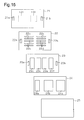
- FIG. 15 is a plan view of a plurality of ceramic sheets, which are elements of a heat dissipation device of the semiconductor device of FIG. 13 .
- FIG. 16 is a perspective view of a second embodiment of a heat dissipation device.
- FIG. 17 is a perspective view of a semiconductor device that includes the heat dissipation device of FIG. 16 .
- FIG. 18 is a cross-sectional view of FIG. 17 taken along line 3 - 3 .
- FIG. 19 is a cross-sectional view of FIG. 17 taken along line 4 - 4 .
- FIG. 20 is a plan view of a plurality of ceramic sheets, which are elements of a base body of the heat dissipation device of FIG. 16 .
- FIG. 21 is a cross-sectional view of another embodiment of a semiconductor device.
- FIGS. 1 to 6 A first embodiment of the present invention will now be described with reference to FIGS. 1 to 6 .
- a semiconductor device 10 shown in FIG. 1 is formed by mounting a metal plate 13 b to which a semiconductor element 13 a is coupled and a metal plate 14 b to which a semiconductor element 14 a is coupled on one surface 12 a (first surface) of a base body 12 of a heat dissipation device 11 .
- the metal plates 13 b and 14 b which function as wiring layers and joining layers, are formed from pure aluminum (e.g., 1000 series aluminum, which is pure aluminum for industrial use) or copper.
- IGBTs insulated gate bipolar transistors
- diodes are used as the semiconductor elements 13 a and 14 a .
- the semiconductor elements 13 a and 14 a are joined with the metal plates 13 b and 14 b by performing metallic joining, for example, soldering or brazing. Also, the metal plates 13 b and 14 b are joined with the heat dissipation device 11 by performing metallic joining, for example, soldering or brazing. In this manner, the metal plates 13 b and 14 b are mounted on the first surface 12 a of the base body 12 .
- locations where the metal plates 13 b and 14 b are mounted are respectively a first mounting portion 121 and a second mounting portion 131 , which function as mounting portions on which the metal plates 13 b and 14 b are mounted. That is, a plurality of the mounting portions (two in the first embodiment) are arranged side by side on the first surface 12 a of the base body 12 .
- the base body 12 is formed by stacking a plurality of ceramic sheets (five sheets in the first embodiment).
- the base body 12 is baked to form the heat dissipation device 11 .
- Aluminum oxide, silicon nitride, silicon carbide, aluminum nitride, alumina zirconium, or the like, is used as the material of the ceramic.
- a ceramic material has high water resistance when water cooling is employed to cool the heat dissipation device 11 .
- the heat dissipation device 11 of the first embodiment includes first to fifth ceramic sheets 21 , 22 , 23 , 24 , and 25 as elements serving as ceramic sheets.
- the first ceramic sheet 21 is located at the upper side
- the fifth ceramic sheet 25 is located at the lower side.
- the first ceramic sheet 21 forms a top plate portion of the heat dissipation device 11 and includes a surface (upper surface) defining the first surface 12 a of the base body 12 .
- a coolant supply hole 21 a and a coolant discharge hole 21 b extend through the first ceramic sheet 21 .
- the coolant supply hole 21 a and the coolant discharge hole 21 b have the same open area.
- the coolant supply hole 21 a is connected to a supply pipe P 1 (shown in FIGS. 1 and 2 ) that supplies a coolant to the heat dissipation device 11 .
- the coolant discharge hole 21 b is connected to a discharge pipe P 2 (shown in FIGS. 1 and 2 ) that discharges the coolant out of the heat dissipation device 11 to the exterior.
- a first coolant inlet hole 22 a extends through the second ceramic sheet 22 .
- the first coolant inlet hole 22 a is located at a position where the first coolant inlet hole 22 a is overlapped with the coolant supply hole 21 a as viewed from a stacking direction of the first to fifth ceramic sheets 21 , 22 , 23 , 24 , and 25 .
- a first coolant outlet hole 22 b extends through the second ceramic sheet 22 .
- the first coolant outlet hole 22 b is located at a position where the first coolant outlet hole 22 b is overlapped with the coolant discharge hole 21 b as viewed from the stacking direction of the first to fifth ceramic sheets 21 , 22 , 23 , 24 , and 25 (hereafter, may be simply referred to as a stacking direction A).
- the first coolant inlet hole 22 a and the first coolant outlet hole 22 b are located in symmetric positions.
- the first coolant inlet hole 22 a and the first coolant outlet hole 22 b have the same open area.
- the second ceramic sheet 22 also includes a plurality of first slits 22 c , which serve as slits, between the first coolant inlet hole 22 a and the first coolant outlet hole 22 b .
- Each first slit 22 c extends through the second ceramic sheet 22 and extends straight in the second ceramic sheet 22 from a position that is closer to the first coolant inlet hole 22 a toward a central portion of the second ceramic sheet 22 .
- the first slits 22 c have the same length.
- the first slits 22 c have the same open area.
- the first slits 22 c are at least partially located underneath the first mounting portion 121 (metal plate 13 b and semiconductor element 13 a ). That is, the first slits 22 c are at least partially overlapped with the first mounting portion 121 as viewed from the stacking direction A.
- the second ceramic sheet 22 also includes a plurality of second slits 22 d , which serve as slits, between the first coolant inlet hole 22 a and the first coolant outlet hole 22 b .
- Each second slit 22 d extends through the second ceramic sheet 22 and extends straight in the second ceramic sheet 22 from a position that is closer to the first coolant outlet hole 22 b toward the central portion of the second ceramic sheet 22 .
- the second slits 22 d have the same length.
- the second slits 22 d have the same open area.
- the second slits 22 d are at least partially located underneath the second mounting portion 131 (metal plate 14 b and semiconductor element 14 a ). That is, the second slits 22 d are at least partially overlapped with the second mounting portion 131 as viewed from the stacking direction A.
- a second coolant inlet hole 23 a extends through the third ceramic sheet 23 .
- the second coolant inlet hole 23 a is located in a position where the second coolant inlet hole 23 a is overlapped with the first coolant inlet hole 22 a as viewed from the stacking direction A.
- a second coolant outlet hole 23 b extends through the third ceramic sheet 23 .
- the second coolant outlet hole 23 b is located in a position where the second coolant outlet hole 23 b is overlapped with the first coolant outlet hole 22 b as viewed from the stacking direction A.
- the second coolant inlet hole 23 a and the second coolant outlet hole 23 b have the same open area.
- the third ceramic sheet 23 also includes a first communication hole 23 c , which extends in a direction orthogonal to the extending direction of each first slit 22 c .
- the first communication hole 23 c is partially overlapped with each first slit 22 c at one end that is located toward the first coolant inlet hole 22 a as viewed from the stacking direction A. This communicates each first slit 22 c and the first communication hole 23 c .
- the third ceramic sheet 23 includes a second communication hole 23 d at a position closer to the second coolant outlet hole 23 b than the first communication hole 23 c .
- the second communication hole 23 d extends in the direction orthogonal to the extending direction of each first slit 22 c .
- the second communication hole 23 d is partially overlapped with each first slit 22 c at the other end, which is located toward the first coolant outlet hole 22 b , as viewed from the stacking direction A. This communicates each first slit 22 c and the second communication hole 23 d.
- the third ceramic sheet 23 also includes a third communication hole 23 e , which extends in a direction orthogonal to the extending direction of each second slit 22 d .
- the third communication hole 23 e is partially overlapped with each second slit 22 d at one end that is located toward the first coolant inlet hole 22 a as viewed from the stacking direction A. This communicates each second slit 22 d and the third communication hole 23 e .
- the third ceramic sheet 23 includes a fourth communication hole 23 f at a position closer to the second coolant outlet hole 23 b than the third communication hole 23 e .
- the fourth communication hole 23 f extends in the direction orthogonal to the extending direction of each second slit 22 d .
- the fourth communication hole 23 f is partially overlapped with each second slit 22 d at the other end, which is located toward the first coolant outlet hole 22 b , as viewed from the stacking direction A. This communicates each second slit 22 d and the fourth communication hole 23 f.
- the fourth ceramic sheet 24 includes a first through hole 24 a , a second through hole 24 b , and a third through hole 24 c .
- the first through hole 24 a is overlapped with the second coolant inlet hole 23 a and a portion of the first communication hole 23 c as viewed from the stacking direction A. This communicates the second coolant inlet hole 23 a and the first communication hole 23 c .
- the second through hole 24 b is overlapped with a portion of the second communication hole 23 d and a portion of the third communication hole 23 e as viewed from the stacking direction A. This communicates the second communication hole 23 d and the third communication hole 23 e .
- the third communication hole 24 c is overlapped with a portion of the fourth communication hole 23 f and the second coolant outlet hole 23 b as viewed from the stacking direction A. This communicates the fourth communication hole 23 f and the second coolant outlet hole 23 b .
- the fifth ceramic sheet 25 forms a bottom plate portion of the heat dissipation device 11 and includes a surface (lower surface) defining a second surface 12 b of the base body 12 . That is, the first surface 12 a and the second surface 12 b are located at opposite sides of the base body 12 .
- the base body 12 of the heat dissipation device 11 is formed by sequentially stacking the fourth ceramic sheet 24 , the third ceramic sheet 23 , the second ceramic sheet 22 , and the first ceramic sheet 21 on the fifth ceramic sheet 25 .
- the interior of the base body 12 includes the coolant supply hole 21 a , the first coolant inlet hole 22 a , the second coolant inlet hole 23 a , the first through hole 24 a , the first communication hole 23 c , each first slit 22 c , the second communication hole 23 d , the second through hole 24 b , the third communication hole 23 e, each second slit 22 d , the fourth communication hole 23 f , the third through hole 24 c , the second coolant outlet hole 23 b, the first coolant outlet hole 22 b , and the coolant discharge hole 21 b , which form a coolant passage 15 through which a coolant flows.
- the coolant supply hole 21 a and the coolant discharge hole 21 b open in the first surface 12 a of the base body 12 .
- the second communication hole 23 d , the second through hole 24 b , and the third communication hole 23 e form a portion of the coolant passage 15 that is located between the first mounting portion 121 and the second mounting portion 131 . That is, the second communication hole 23 d , the second through hole 24 b , and the third communication hole 23 e form a portion of the coolant passage 15 that extends from the first mounting portion 121 toward the second surface 12 b and extends from the second surface 12 b toward the second mounting portion 131 .
- the second ceramic sheet 22 corresponds to a slit formation layer that includes the first slits 22 c and the second slits 22 d , which form a portion of the coolant passage 15 .
- the first communication hole 23 c corresponds to a communication passage that is overlapped with each first slit 22 c at a portion closer to the first coolant inlet hole 22 a and communicates with each first slit 22 c .
- the second communication hole 23 d corresponds to a communication passage that is overlapped with each first slit 22 c at a portion closer to the first coolant outlet hole 22 b and communications with each first slit 22 c .
- the third communication hole 23 e corresponds to a communication passage that is overlapped with each second slit 22 d at a portion closer to the first coolant inlet hole 22 a and communicates with each second slit 22 d .
- the fourth communication hole 23 f corresponds to a communication passage that is overlapped with each second slit 22 d at a portion closer to the first coolant outlet hole 22 b and communicates with each second slit 22 d .
- the third ceramic sheet 23 corresponds to a communication passage formation layer that includes the first communication hole 23 c , the second communication hole 23 d , the third communication hole 23 e , and the fourth communication hole 23 f , which correspond to the communication passages.
- the first slits 22 c and the second slits 22 d are located toward the first mounting portion 121 and the second mounting portion 131 from the first communication hole 23 c, the second communication hole 23 d , the third communication hole 23 e , and the fourth communication hole 23 f in the stacking direction A.
- the second communication hole 23 d is continuous to the first slit 22 c at a downstream side of the coolant flow
- the second through hole 24 b is continuous to the second communication hole 23 d .
- the extension passage W includes a passage surface X 1 and a passage surface Y 1 that are opposed in the stacking direction of the first to fifth ceramic sheets 21 to 25 .
- the passage surface X 1 is a portion of a passage formed by the first slit 22 c, which is located closer to the first surface 12 a of the base body 12 .
- the passage surface Y 1 is a portion of a passage formed by the second through hole 24 b , which is located closer to the second surface 12 b.
- the passage surface X 1 is formed by a surface of the first ceramic sheet 21 , which is located above the second ceramic sheet 22 .
- the passage surface Y 1 is formed by a surface of the fifth ceramic sheet 25 , which is located below the fourth ceramic sheet 24 . That is, a passage formed by the first slit 22 c forms the coolant passage 15 that is located on the uppermost position in the stacking direction.
- the passage surface X 1 corresponds to an upper surface of the passage.
- a passage formed by the second through hole 24 b forms the coolant passage 15 that is located at the lowermost position in the stacking direction.
- the passage surface Y 1 corresponds to a lower surface of the passage.
- a first fin 31 is located between adjacent ones of the first slits 22 c .
- a second fin 32 is located between adjacent ones of the second slits 22 d.
- the length H of the first fin 31 (length of the first slit 22 c ) is set to be within a region Z (dotted region in FIG. 6 ) as viewed from the stacking direction A.
- the region Z is located between straight lines A and B.
- the straight lines A and B extend from opposite ends 131 b and 132 b of the metal plate 13 b at an angle ⁇ of 45° relative to the first surface 12 a of the base body 12 .
- the angle ⁇ of the straight lines A and B relative to the first surface 12 a of the base body 12 only needs to be within 30° to 60°.
- the region Z which is located between the straight lines A and B, forms a heat transmission region where the heat generated by the semiconductor element 13 a is transmitted to the heat dissipation device 11 through the metal plate 13 b.
- a portion of the first communication hole 23 c that corresponds to the region Z as viewed from the stacking direction A serves as an overlapping portion 35 of each first slit 22 c and the first communication hole 23 c .
- the overlapping portion 35 is located in the heat transmission region, where the heat generated by the semiconductor element 13 a is transmitted to the heat dissipation device 11 through the metal plate 13 b. That is, the overlapping portion 35 is located proximate to a region where the first mounting portion 121 is located as viewed from the stacking direction A.
- the overlapping portion 35 is located toward an inner side of the first slit 22 c from one end 221 c of each first slit 22 c that is closer to the first coolant inlet hole 22 a .
- the same description can be given for the length of the second fin 32 (length of the second slit 22 d ) and an overlapping portion 36 of each second slit 22 d and the third communication hole 23 e as the length H of the first fin 31 and the overlapping portion 35 of each first slit 22 c and the first communication hole 23 c. Thus, a detailed description will not be given.
- the overlapping portion 35 includes a first overlapping portion 35 a , which is located underneath the first mounting portion 121 , and a second overlapping portion 35 b , which excludes the first overlapping portion 35 a .
- the length of the second overlapping portion 35 b is greater than the length of the first overlapping portion 35 a .
- the phrase “the length of the second overlapping portion 35 b is greater than the length of the first overlapping portion 35 a ” means, in the cross-sectional view of the heat dissipation device 11 , the second overlapping portion 35 b extends toward the first coolant inlet hole 22 a , which results in the length of the second overlapping portion 35 b being greater than the length of the first overlapping portion 35 a .
- the first mounting portion 121 has been described here, the second mounting portion 131 has the same form.
- the phrase of “underneath a mounting portion” refers to a region that is located toward the coolant passage 15 from the mounting portion and corresponds to a region that is overlapped with the mounting portion as viewed from the stacking direction A.
- the coolant supplied from the coolant supply source flows from the supply pipe P 1 to each first slit 22 c through the coolant supply hole 21 a , the first coolant inlet hole 22 a , the second coolant inlet hole 23 a , the first through hole 24 a , and the first communication hole 23 c .
- the coolant flows from the first communication hole 23 c to each first slit 22 c
- the coolant is expelled from the first communication hole 23 c into each first slit 22 c and directed toward the first mounting portion 121 (semiconductor element 13 a and metal plate 13 b ).
- the semiconductor element 13 a corresponds to a first cooling subject.
- the coolant flows from each first slit 22 c to each second slit 22 d through the second communication hole 23 d, the second through hole 24 b , and the third communication hole 23 e .
- the coolant flows from the third communication hole 23 e to each second slit 22 d
- the coolant is expelled from the third communication hole 23 e into each second slit 22 d to be directed toward the second mounting portion 131 (semiconductor element 14 a and metal plate 14 b ).
- This generates a jet flow in the coolant flowing from the third communication hole 23 e to each second slit 22 d and agitates the coolant flowing through each second slit 22 d .
- the heat which is transmitted from semiconductor element 14 a to the heat dissipation device 11 (each second fin 32 ) through the metal plate 14 b , is dissipated to the coolant flowing through each second slit 22 d more effectively then when, for example, the coolant flows through each second slit 22 d along the second mounting portion 131 (first surface 12 a of the base body 12 ) after flowing along the first surface 12 a .
- the semiconductor element 14 a corresponds to a second cooling subject.
- the coolant flows through each second slit 22 d and is discharged from the discharge pipe P 2 and out of the heat dissipation device 11 through the fourth communication hole 23 f , the third through hole 24 c , the second coolant outlet hole 23 b , the first coolant outlet hole 22 b , and the coolant discharge hole 21 b.
- the first embodiment has the advantages described below.
- the first slit 22 c and the second slit 22 d are located toward the first mounting portion 121 and the second mounting portion 131 from the first communication hole 23 c, the second communication hole 23 d , the third communication hole 23 e , and the fourth communication hole 23 f in the stacking direction A.
- the overlapping portion 35 of each first slit 22 c and the first communication hole 23 c and the overlapping portion 36 of each second slit 22 d and the third communication hole 23 e are respectively located proximate to regions where the first mounting portion 121 and the second mounting portion 131 are arranged.
- the coolant flowing from the first communication hole 23 c to each first slit 22 c may be directed toward the first mounting portion 121 .
- the coolant flowing from the third communication hole 23 e to each second slit 22 d may be directed toward the second mounting portion 131 .
- the performance for cooling the semiconductor elements 13 a and 14 a may be improved.
- the length of the second overlapping portion 35 b is greater than the length of the first overlapping portion 35 a .
- the length of the second overlapping portion 35 b is greater than the length of the first overlapping portion 35 a . This allows the coolant to cool the heat transmission region from a portion located at the upstream side and effectively cools the semiconductor element 13 a . Thus, the performance for cooling the semiconductor element 13 a may be improved.
- the same advantage may be obtained even when a plurality of semiconductor elements are mounted on each mounting portion.
- a portion of the coolant passage 15 that is formed by the second communication hole 23 d , the second through hole 24 b , and the third communication hole 23 e extends from the first mounting portion 121 in a direction toward the second surface 12 b and extends from the second surface 12 b in a direction toward the second mounting portion 131 .
- the flow of the coolant flowing through the coolant passage 15 may be directed toward the first mounting portion 121 and the second mounting portion 131 .
- the semiconductor elements 13 a and 14 a can be effectively cooled and the performance for cooling the semiconductor elements 13 a and 14 a may be improved.
- the first communication hole 23 c and the first slit 22 c , and the third communication hole 23 e and the second slit 22 d are each directed to the corresponding mounting portion in a stepped manner.
- the stepped coolant passage 15 can generate a jet flow and a turbulent flow in the coolant. This effectively cools each first slit 22 c from the end 221 c , which is located at the upstream side, and each second slit 22 d from an end of the passage surface X 1 that is located at the upstream side.
- the cooling performance may be improved. This reduces the size of the heat dissipation device 11 without the need to lengthen the passage to improve the cooling performance.
- the coolant supply hole 21 a and the coolant discharge hole 21 b open in the first surface 12 a of the base body 12 .
- components needed for the heat dissipation device 11 may be collectively located at the side of the first surface 12 a of the base body 12 . This reduces the size of the heat dissipation device 11 .
- the length H of the first fin 31 (length of the first slit 22 c ) is set to be within the region Z as viewed from the stacking direction A.
- the region Z is located between the straight lines A and B, which extend from the opposite ends 131 b and 132 b of the metal plate 13 b at an angle ⁇ of 45° relative to the first surface 12 a of the base body 12 .
- the length H of the first fin 31 may be the minimum length needed for the heat dissipation of the semiconductor element 13 a . That is, the length of the first slit 22 c can be minimized. This limits pressure loss of the coolant flowing through the first slit 22 c as compared to when the first slit 22 c is formed to extend beyond the region Z to a position outside the region Z.
- the passage surfaces X 1 and Y 1 are opposed to each other in the stacking direction. This reduces portions that decrease the area of the passage. Thus, the pressure loss of the coolant may be decreased.
- the extension passage W becomes almost straight in the stacking direction A.
- the reduction of steps in the extension passage W limits expansion of the coolant passage 15 in the lateral direction. This decreases the size of the heat dissipation device 11 .
- the first embodiment may be modified as follows.
- the second ceramic sheet 22 may include a communication portion 22 h that communicates each first slit 22 c and each second slit 22 d .
- the second communication hole 23 d , the second through hole 24 b , and the third communication hole 23 e may be removed.
- the coolant may flow from each first slit 22 c to each second slit 22 d through the communication portion 22 h only in the second ceramic sheet 22 .
- the pressure loss of the coolant may be limited.
- a metal plate including a semiconductor element that should be cooled the most is mounted on the first mounting portion 121 .
- the open area of the first communication hole 23 c may be set to be smaller than that of the first embodiment. This increases the flow speed of the coolant when passing through the first communication hole 23 c . In this case, jet flow may be generated in the coolant flowing from the first communication 23 c to each first slit 22 c . As a result, the performance for cooling the semiconductor element 13 a may be further improved.
- the open area of the third communication hole 23 e may be set to be smaller than that of the first embodiment. This increases the flow speed of the coolant when passing through the third communication hole 23 e.
- the open area of the first through hole 24 a may be set to be larger than that of the first embodiment.
- the open area of the second through hole 24 b may be set to be larger than that of the first embodiment.
- a third mounting portion 171 which serves as a mounting portion, may be additionally located on a position of the second surface 12 b that is located beyond a portion of the coolant passage 15 that is located between the first mounting portion 121 and the second mounting portion 131 and extends in a direction from the first mounting portion 121 toward the second surface 12 b of the base body 12 .
- the second through hole 24 b is replaced with a plurality of slits 41 , and a plurality of fins 42 are arranged in the fourth ceramic sheet 24 .
- the fins 42 are at least partially overlapped with the third mounting portion 171 as viewed from the stacking direction A.
- a metal plate 17 b to which a semiconductor element 17 a is coupled is mounted on the third mounting portion 171 .
- the semiconductor element 17 a is cooled by dissipating heat to the coolant flowing through the slits 41 .
- the semiconductor element 17 a corresponds to a third cooling subject.
- the maximum number of semiconductor elements may be mounted on the heat dissipation device 11 , the total volume may be reduced, and the performance for cooling the semiconductor elements 13 a , 14 a , and 17 a , which are mounted on the heat dissipation device 11 , may be improved.
- the second ceramic sheet 22 may include a plurality of first slits 43 and second slits 44 , each of which are undulated. This increases the heat dissipation surface area as compared to the first slits 22 c and the second slits 22 d , which are straight in a plan view. Also, the agitation effect is obtained. This further improves the performance for cooling the semiconductor elements 13 a and 14 a.
- the positions of the coolant supply hole and the coolant discharge hole of the coolant passage 15 may be changed.
- the coolant supply hole and the coolant discharge hole may open in the second surface 12 b of the base body 12 .
- the first slits 22 c and the second slits 22 d only need to be at least partially overlapped with a region that includes the first mounting portion 121 and the second mounting portion 131 as viewed from the stacking direction A.
- the number of the first slits 22 c and the second slits 22 d may be changed.
- the number of slits is changed in accordance with the area of a semiconductor element, the passage width of the coolant passage 15 , and the like. For example, when the region area forming the coolant passage 15 is the same, the number of slits decreases if the passage width increases, and the number of slits increases if the passage width decreases.
- the number of ceramic sheets that are stacked to form the base body 12 of the heat dissipation device 11 may be changed.
- the number of ceramic sheets stacked is increased or decreased in accordance with the cross-sectional area (passage area) of the coolant passage 15 formed in the heat dissipation device 11 .
- the first embodiment does not particularly limit the number of semiconductor elements or metal plates.
- the first embodiment does not particularly limit the number of mounting portions.
- the heat dissipation device 11 may be cooled by undergoing air cooling.
- a cooling gas such as air, flows to the coolant passage 15 .
- the heat dissipation device 11 of the first embodiment shown in FIG. 4 may include an extension passage, which has the same structure as the extension passage W, at the side of the second slit 22 d in addition to the extension passage W connected to the first slit 22 c.
- extension passages W 1 and W 2 extending straight in the stacking direction of the first to fifth ceramic sheets 21 to 25 may be arranged as the extension passage W.
- the extension passage W 1 is a portion of the coolant passage 15 that is formed by the first slit 22 c , the second communication hole 23 d , and the second through hole 24 b .
- the extension passage W 2 is a portion of the coolant passage 15 that is formed by the second slit 22 d , the fourth communication hole 23 f , and the third through hole 24 c . As shown in FIG.
- the passage surface X 1 which is formed by a surface of the first ceramic sheet 21
- the passage surface Y 1 which is formed by a surface of the fifth ceramic sheet 25 .
- the straight extension passages W 1 and W 2 further decrease the pressure loss of the coolant compared to when the passage is formed in a stepped manner. Also, the reduction of steps further limits expansion of the coolant passage 15 in the lateral direction. This further decreases the size of the heat dissipation device 11 .
- the position of the second communication hole 23 d at an end (end that is located closer to the second coolant outlet hole 23 b ) opposite to the end that is located closer to the second coolant inlet hole 23 a is aligned with the position of the first slit 22 c at an end (end that is located closer to the first coolant outlet hole 22 b ) opposite to the end that is located closer to the first coolant inlet hole 22 a .
- the position of the second communication hole 23 d at the end that is located closer to the second coolant inlet hole 23 a is aligned with the position of the second through hole 24 b at an end that is located closer to the first through hole 24 a .
- the position of the fourth communication hole 23 f at an end that is located closer to the second coolant outlet hole 23 b is aligned with the position of the second slit 22 d at an end that is located closer to the first coolant outlet hole 22 b .
- the position of the fourth communication hole 23 f at an end (end that is located closer to the second coolant inlet hole 23 a ) opposite to the end that is located closer to the second coolant outlet hole 23 b is aligned with the position of the third through hole 24 c at an end that is located closer to the second through hole 24 b.
- FIGS. 16 to 20 A second embodiment of the present invention will now be described with reference to FIGS. 16 to 20 .
- a heat dissipation device 11 includes a base body 218 , which is formed by stacking a plurality of sheets (six sheets in the second embodiment) of first to sixth ceramic members 212 , 213 , 214 , 215 , 216 , and 217 .
- a ceramic material has high water resistance when water cooling is employed to cool the heat dissipation device 11 .
- the base body 218 includes a coolant supply hole 219 and a coolant discharge hole 220 .
- a coolant is supplied from the exterior to a coolant passage formed in the base body 218 through the coolant supply hole 219 .
- the coolant flowing through the coolant passage is discharged from the coolant passage to the outside of the base body 218 through the coolant discharge hole 220 .
- the coolant supply hole 219 and the coolant discharge hole 220 each open in the first ceramic member 212 , which is an element of the base body 218 . That is, the coolant supply hole 219 and the coolant discharge hole 220 each open in one surface (first surface) of the base body 218 .
- the coolant supply hole 219 is connectable to the supply pipe P 1 , which is connected to an external coolant supply source.
- the coolant discharge hole 220 is connectable to the discharge pipe P 2 , which discharges the coolant to the exterior.
- the base body 218 also includes a mounting portion 222 (indicated by broken lines in FIG. 16 ) of an electronic component 221 at a position where the mounting portion 222 is at least partially overlapped with the coolant passage as viewed from a stacking direction of the first to sixth ceramic members 212 , 213 , 214 , 215 , 216 , and 217 (hereafter, may be simply referred to as a stacking direction B).
- the mounting portion 222 is arranged on a surface (first face) of the first ceramic member 212 located at the exterior of the base body 218 in which the coolant supply hole 219 and the coolant discharge hole 220 open.
- a semiconductor device 10 is formed by mounting a metal plate 227 on the mounting portion 222 located on the base body 218 of the heat dissipation device 11 .
- a semiconductor element 226 which serves as the electronic component 221 , is coupled to the metal plate 227 .
- the metal plate 227 which functions as a wiring layer and a bonding layer, is pure aluminum (e.g., 1000 series aluminum, which is pure aluminum for industrial use) or copper.
- the semiconductor element 226 is, for example, an insulated gate bipolar transistor (IGBT) or a diode.
- the semiconductor element 226 and the metal plate 227 , and the metal plate 227 and the heat dissipation device 11 are each joined by performing metallic joining, for example, soldering or brazing.
- the heat dissipation device 11 of the second embodiment will now be described in detail.
- a coolant passage 228 that communicates the coolant supply hole 219 and the coolant discharge hole 220 is formed in the base body 218 of the heat dissipation device 11 .
- the first ceramic member 212 which is the element of the base body 218 and includes the mounting portion 222 , is located at the upper side
- the sixth ceramic sheet 217 which is located at the farthest position from the first ceramic member 212 , is located at the lower side.
- the coolant passage 228 includes first to seventh passages L 1 to L 7 . More specifically, the first passage L 1 is straight and continuous to the coolant supply hole 291 . The coolant flows through the first passage L 1 in a vertically lower direction. The second passage L 2 branches from the first passage L 1 . The coolant flows through the second passage L 2 obliquely upward. The third passage L 3 is straight, continuous to the second passage L 2 , and formed underneath the mounting portion 222 . The coolant flows through the third passage L 3 in the horizontal direction. The fourth passage L 4 is straight and continuous to the third passage L 3 . The coolant flows through the fourth passage L 4 in the vertically lower direction. The fifth passage L 5 is straight and continuous to the fourth passage L 4 .
- the coolant flows through the fifth passage L 5 in the horizontal direction.
- the sixth passage L 6 is straight and continuous to the fifth passage L 5 .
- the coolant flows through the sixth passage L 6 in a vertically direction.
- the seventh passage L 7 is straight and branches from the first passage L 1 together with the second passage L 2 .
- the coolant flows through the seventh passage L 7 from the vertically lower side to the vertically upper side toward the third passage L 3 located underneath the mounting portion 222 .
- the first to sixth ceramic members 212 to 217 includes a plurality of passage holes, which are elements of the coolant passage 228 .
- the passage holes are joined in the stacking direction of the first to sixth ceramic members 212 to 217 to form the first to seventh passages L 1 to L 7 .
- FIG. 20 a sheet forming the ceramic member is referred to as a ceramic sheet.
- the same reference numeral as the ceramic member is given to the ceramic sheet.
- the first to sixth ceramic sheets 212 to 217 which are elements of the heat dissipation device 11 , are rectangle and have the same length and the same width.
- the first ceramic sheet 212 forms a top plate of the heat dissipation device 11 where the mounting portion 222 is located.
- a first passage hole 212 a including the coolant supply hole 219 and a sixth passage hole 212 b including the coolant discharge hole 220 are located at opposite ends of the mounting portion 222 .
- the first passage hole 212 a and the sixth passage hole 212 b have the same open area.
- the second ceramic sheet 213 is located below the first ceramic sheet 212 when stacked.
- the second ceramic sheet 213 includes a first passage hole 213 a and a sixth passage hole 213 b .
- the first passage hole 213 a is located at a position corresponding to the first passage hole 212 a of the first ceramic sheet 212 and communicates with the first passage hole 212 a .
- the first passage hole 213 a has the same open area as the first passage hole 212 a .
- the sixth passage hole 213 b is located at a position corresponding to the sixth passage hole 212 b of the first ceramic sheet 212 and communicates with the sixth passage hole 212 b .
- the sixth passage hole 213 b has the same open area as the sixth passage hole 212 b .
- the second ceramic sheet 213 includes a plurality of slit-like third passage holes 213 c (five slits in the second embodiment) between the first passage hole 213 a and the sixth passage hole 213 b .
- Each third passage hole 213 c has the same shape and extends straight.
- the length of the third passage hole 213 c in the extending direction (longitudinal direction) is greater than the length of the mounting portion 222 in the same direction.
- the third passage holes 213 c are arranged along a direction orthogonal to the extending direction (longitudinal direction) at regular intervals. As shown in FIGS. 18 and 19 , a portion of the third passage hole 213 c is located underneath the mounting portion 222 .
- the other portion of the third passage hole 213 c is located outside the mounting portion 222 as viewed from the stacking direction B.
- the third ceramic sheet 214 is located below the second ceramic sheet 213 when stacked.
- the third ceramic sheet 214 includes a first passage hole 214 a and a sixth passage hole 214 b .
- the first passage hole 214 a is located at a position corresponding to the first passage hole 213 a of the second ceramic sheet 213 and communicates with the first passage hole 213 a .
- the first passage hole 214 a has the same open area as the first passage hole 213 a .
- the sixth passage hole 214 b communicates with the sixth passage hole 213 b of the second ceramic sheet 213 and has the same open area as the sixth passage hole 213 b .
- the third ceramic sheet 214 also includes a plurality of slit-like third passage holes 214 c (five slits in the second embodiment) between the first passage hole 214 a and the sixth passage hole 214 b .
- Each third passage hole 214 c has the same shape and extends straight.
- Each third passage hole 214 c is located in a position where the third passage hole 214 c is partially overlapped with the third passage hole 213 c of the second ceramic sheet 213 as viewed from the stacking direction B.
- the length of each third passage hole 214 c in the extending direction is greater than the length of the third passage hole 213 c of the second ceramic sheet 213 in the same direction.
- the third passage holes 214 c are arranged along a direction orthogonal to the extending direction (longitudinal direction) at regular intervals.
- opposite ends of the third passage hole 214 c are located at positions that are projected by the same length outward from opposite ends of the third passage hole 213 c as viewed from the stacking direction B.
- each third passage hole 213 c are overlapped with each third passage hole 214 c in the stacking direction. This forms the third passage L 3 , which has the height of two ceramic sheets.
- the fourth ceramic sheet 215 is located below the third ceramic sheet 214 when stacked.
- the fourth ceramic sheet 215 includes a first passage hole 215 a .
- the first passage hole 215 a is located at a position where the first passage hole 215 a is entirely overlapped with the first passage hole 214 a and partially overlapped with the third passage hole 214 c that is located closer to the first passage hole 214 a as viewed from the stacking direction B.
- the open area of the first passage hole 215 a is greater than the open area of the first passage hole 214 a of the third ceramic sheet 214 .
- the length of the first passage hole 215 a in a direction orthogonal to the extending direction of the third passage hole 214 c of the third ceramic sheet 214 is the same as the length between inner surfaces of the third passage holes 214 c that are located at the opposite outermost positions.
- the fourth ceramic sheet 215 includes a sixth passage hole 215 b .
- the sixth passage hole 215 b is located at a position corresponding to the sixth passage hole 214 b of the third ceramic sheet 214 and communicates with the sixth passage hole 214 b .
- the sixth passage hole 215 b has the same open area as the sixth passage hole 214 b .
- the fourth ceramic sheet 215 also includes a fourth passage hole 215 c between the first passage hole 215 a and the sixth passage hole 215 b.
- the fourth passage hole 215 c is located in a position where the fourth passage hole 215 c is partially overlapped with each third passage hole 214 c that is located closer to the sixth passage hole 214 b as viewed from the stacking direction B.
- the fourth ceramic sheet 215 also includes a plurality of slit-like seventh passage holes 215 d (five slits in the second embodiment) between the first passage hole 215 a and the fourth passage hole 215 c .
- Each seventh passage hole 215 d has the same shape and extends straight.
- Each seventh passage hole 215 d is located in a position where the seventh passage hole 215 d is overlapped with the third passage hole 214 c of the third ceramic sheet 214 as viewed from the stacking direction B.
- the length of each seventh passage hole 215 d in the extending direction is less than the length of each of the third passage holes 213 c and 214 c of the second and third ceramic sheets 213 and 214 in the same direction.
- the seventh passage holes 215 d are arranged along a direction orthogonal to the extending direction (longitudinal direction) at regular intervals.
- the centers of the seventh passage holes 215 d are arranged along a line that extends through the center of the mounting portion 222 in a direction orthogonal to the extending direction of the third passage holes 213 c and 214 c.
- the fifth ceramic sheet 216 is located below the fourth ceramic sheet 215 when stacked.
- the fifth ceramic sheet 216 includes a first passage hole 216 a and a fifth passage hole 216 b .
- the first passage hole 216 a is located at a position where the first passage hole 216 a is entirely overlapped with the first passage hole 215 a and each seventh passage hole 215 d as viewed from the stacking direction B.
- the fifth passage hole 216 b is located at a position where the fifth passage hole 216 b is entirely overlapped with the sixth passage hole 215 b and the fourth passage hole 215 c as viewed from the stacking direction B.
- the sixth ceramic sheet 217 is located below the fifth ceramic sheet 216 when stacked.
- the sixth ceramic sheet 217 forms a bottom plate of the heat dissipation device 11 .
- the base body 218 of the heat dissipation device 11 is formed by sequentially stacking the fifth ceramic member 216 , the fourth ceramic member 215 , the third ceramic member 214 , the second ceramic member 213 , and the first ceramic member 212 on the sixth ceramic member 217 .
- the coolant passage 228 is formed in the base body 218 having such a structure.
- the first passage L 1 is formed by connecting each first passage hole 212 a , 213 a , 214 a , 215 a , 216 a of the first to fifth ceramic members 212 to 216 .
- the second passage L 2 is formed by connecting a portion of the first passage hole 215 a of the fourth ceramic member 215 , a portion of the third passage hole 214 c of the third ceramic member 214 , and a portion of the third passage hole 213 c of the second ceramic member 213 in a stepped manner.
- the third passage L 3 is formed by connecting the third passage hole 213 c of the second ceramic member 213 and the third passage hole 214 c of the third ceramic member 214 .
- the fourth passage L 4 is formed by connecting a portion of the third passage hole 214 c of the third ceramic member 214 , the fourth passage hole 215 c of the fourth ceramic member 215 , and a portion of the fifth passage hole 216 b of the fifth ceramic member 216 in a straight line.
- the fifth passage L 5 is formed by the fifth passage hole 216 b of the fifth ceramic member 216 , which is connected to the fourth passage hole 215 c of the fourth ceramic member 215 .
- the sixth passage L 6 is connected to the fifth passage hole 216 b of the fifth ceramic member 216 and formed by connecting each sixth passage hole 212 b , 213 b , 214 b , 215 b of the first to fourth ceramic members 212 to 215 .
- the seventh passage L 7 is formed by the seventh passage holes 215 d of the fourth ceramic member 215 , which are connected to the first passage hole 216 a of the fifth ceramic member 216 .
- the third passage L 3 of the second embodiment serves as an underneath-lying passage through which coolant flows underneath the mounting portion 222 .
- the second passage L 2 of the second embodiment is in communication with the third passage L 3 at the upstream side in a flow direction of the coolant and forms a supply passage that supplies the coolant to the third passage L 3 together with the first passage L 1 connected to the second passage L 2 .
- the fourth passage L 4 of the second embodiment is in communication with the third passage L 3 at the downstream side in the flow direction of the coolant and forms a discharge passage that discharges the coolant from the third passage L 3 together with the fifth passage L 5 connected to the fourth passage L 4 and the sixth passage L 6 connected to the fifth passage L 5 .
- the seventh passage L 7 of the second embodiment is located between the supply passage and the discharge passage and serves as an expulsion passage that expels the coolant to the third passage L 3 from the vertically lower side toward the vertically upper side.
- the seventh passage L 7 serving as the expulsion passage expels the coolant toward a central section of the mounting portion 222 .
- the base body 218 includes fins 230 and 231 .
- the fin 230 is located between the third passage holes 213 c of the second ceramic member 213 forming the third passage L 3 .
- the fin 231 is located between the third passage holes 214 c of the third ceramic member 214 forming the third passage L 3 .
- the fins 230 and 231 are overlapped in the stacking direction B.
- the fins 230 and 231 are straight fins.
- the coolant supplied through the coolant supply hole 219 to the coolant passage 228 first flows through the first passage L 1 toward a lower side of the heat dissipation device 11 .
- the coolant in the first passage L 1 is separated to flow into the second passage L 2 and the seventh passage L 7 , which branch from the first passage L 1 .
- the coolant flows from the second passage L 2 and the seventh passage L 7 to the third passage L 3 .
- the heat of the electronic component 221 (semiconductor element 226 and metal plate 227 ) is dissipated to the coolant flowing through the third passage L 3 by way of the surface of the first ceramic member 212 , which covers the third passage L 3 , and the fins 230 and 231 .
- the coolant flows from the third passage L 3 through the fourth passage L 4 , the fifth passage L 5 , and the sixth passage L 6 , and out of the coolant discharge hole 220 .
- the heat dissipation device 11 of the second embodiment includes the second passage L 2 , through which the coolant flows toward the third passage L 3 in an oblique direction from a peripheral region of the mounting portion 222 of the electronic component 221 toward the mounting portion 222 , and the seventh passage L 7 , through which the coolant flows toward the central section of the mounting portion 222 from the lower side to the upper side.
- the coolant flowing through the second passage L 2 and the seventh passage L 7 are expelled toward the third passage L 3 from the lower side to the upper side. This generates a jet flow in the coolant flowing through the third passage L 3 and agitates the coolant.
- the agitation thins a temperature boundary layer of the coolant flowing through the third passage L 3 .
- the coolant is expelled from the seventh passage L 7 toward the central portion of the electronic component 221 , which has the highest temperature in the mounting portion 222 . This allows the coolant to directly strike a heating surface and effectively thins the temperature boundary layer.
- the second embodiment has the advantages described below.
- the seventh passage L 7 is arranged to expel the coolant into the third passage L 3 from the vertically lower side to the vertically upper side. This allows the coolant to directly strike a location corresponding to the mounting portion 222 . This effectively agitates the coolant flowing through the third passage L 3 and thins the temperature boundary layer of the coolant flowing through the third passage L 3 . Thus, the performance for cooling the cooling subject can be improved.
- the seventh passage L 7 branches from the first passage L 1 . This simplifies the structure of the coolant passage 228 formed in the base body 218 .
- the seventh passage L 7 expels the coolant toward the central section of the mounting portion 222 . This effectively thins the temperature boundary layer of the coolant flowing through the third passage L 3 . Thus, the performance for cooling the cooling subject can be further improved.
- the coolant supply hole 219 and the coolant discharge hole 220 open in the surface (first surface) of the base body 218 where the mounting portion 222 is arranged. This allows for a collective arrangement of components needed for the heat dissipation device 11 , such as, the supply pipe P 1 connected to the coolant supply hole 219 , and the discharge pipe P 2 connected to the coolant discharge hole 220 . As a result, the heat dissipation device 11 can be reduced in size.
- the straight fourth passage L 4 decreases pressure loss of the coolant as compared to when the fourth passage L 4 includes steps. Also, the straight fourth passage L 4 reduces steps in the coolant passage 228 and limits expansion of the coolant passage 228 in the lateral direction. This reduces the size of the heat dissipation device 11 .
- the semiconductor device 10 having the heat dissipation device 11 can effectively cool the electronic component 221 (semiconductor element 226 and metal plate 227 ). This improves the performance for cooling the electronic component 221 .
- the ceramic heat dissipation device 11 may have a cooling function and an insulative property. This allows for the formation of the semiconductor device 10 by directly joining the heat dissipation device 11 with the electronic component 221 (semiconductor element 226 and metal plate 227 ). Thus, the semiconductor device 10 may be reduced in size and the number of components.
- the second embodiment may be modified as follows.
- a plurality of the seventh passages L 7 may be arranged in the coolant passage 228 .
- coolant expelling positions of the seventh passages L 7 are located within the region of the mounting portion 222 as viewed from the stacking direction B. This further increases the effect of the jet flow.
- at least one of the seventh passages L 7 is located in a position where the coolant is expelled toward the central section of the mounting portion 222 .
- the seventh passages L 7 allow the coolants to directly strike a location corresponding to the mounting portion 222 from a wide range. This effectively thins the temperature boundary layer of the coolant flowing through the third passage L 3 and further improves the performance for cooling the cooling subject.
- the base body 218 may include undulated fins by forming undulated third passage holes 213 c and 214 c .
- the undulated fins increase the area that contacts the coolant and has a coolant agitating effect. This improves the cooling performance.
- a passage that supplies the coolant to the second passage L 2 may differ from a passage that supplies the coolant to the seventh passage L 7 .
- the coolant may be directly supplied to the seventh passage L 7 from the exterior.
- the coolant supply hole 219 and the coolant discharge hole 220 may be located at different positions in the base body 218 .
- the coolant supply hole 219 and the coolant discharge hole 220 may be located in the sixth ceramic member 217 .
- One of the coolant supply hole 219 and the coolant discharge hole 220 may be located in the first ceramic member 212 when the other is located in the sixth ceramic member 217 .
- the fourth passage L 4 may extend obliquely downward by connecting a portion of the third passage hole 214 c of the third ceramic member 214 , the fourth passage hole 215 c of the fourth ceramic member 215 , and a portion of the fifth passage hole 216 b of the fifth ceramic member 216 in a stepped manner.
- the number of the third passage holes 213 c and 214 c may be changed.
- the number is changed in accordance with the area of a semiconductor element, the passage width of the coolant passage 228 , and the like. For example, when the area of the region forming the coolant passage 228 is the same, the number of the third passage holes 213 c and 214 c decreases if the passage width increases, and the number increases if the passage width decreases.
- the number of ceramic members that are stacked to form the base body 218 of the heat dissipation device 11 may be changed.
- the number of ceramic members stacked is increased or decreased in accordance with the cross-sectional area (passage area) of the coolant passage 228 formed in the heat dissipation device 11 .
- the heat dissipation device 11 may be cooled by undergoing liquid cooling or air cooling.
- the number of the electronic components 221 mounted on the heat dissipation device 11 may be changed.
- the coolant passage 228 in the base body 218 may be modified in accordance with the number or the layout of the mounting portions 222 on which the electronic components 221 are mounted.
Landscapes
- Engineering & Computer Science (AREA)
- Computer Hardware Design (AREA)
- Microelectronics & Electronic Packaging (AREA)
- Power Engineering (AREA)
- Physics & Mathematics (AREA)
- Condensed Matter Physics & Semiconductors (AREA)
- General Physics & Mathematics (AREA)
- Chemical & Material Sciences (AREA)
- Ceramic Engineering (AREA)
- Materials Engineering (AREA)
- Cooling Or The Like Of Semiconductors Or Solid State Devices (AREA)
- Cooling Or The Like Of Electrical Apparatus (AREA)
Applications Claiming Priority (7)
| Application Number | Priority Date | Filing Date | Title |
|---|---|---|---|
| JP2012-159734 | 2012-07-18 | ||
| JP2012159734 | 2012-07-18 | ||
| JP2012-284012 | 2012-12-27 | ||
| JP2012-284011 | 2012-12-27 | ||
| JP2012284011 | 2012-12-27 | ||
| JP2012284012 | 2012-12-27 | ||
| PCT/JP2013/069515 WO2014014054A1 (ja) | 2012-07-18 | 2013-07-18 | 放熱装置、及び半導体装置 |
Publications (2)
| Publication Number | Publication Date |
|---|---|
| US20150221579A1 US20150221579A1 (en) | 2015-08-06 |
| US9646915B2 true US9646915B2 (en) | 2017-05-09 |
Family
ID=49948877
Family Applications (1)
| Application Number | Title | Priority Date | Filing Date |
|---|---|---|---|
| US14/414,728 Expired - Fee Related US9646915B2 (en) | 2012-07-18 | 2013-07-18 | Heat dissipation device and semiconductor device |
Country Status (6)
| Country | Link |
|---|---|
| US (1) | US9646915B2 (ko) |
| EP (1) | EP2876678A4 (ko) |
| JP (1) | JP6124890B2 (ko) |
| KR (1) | KR101624523B1 (ko) |
| CN (1) | CN104471706A (ko) |
| WO (1) | WO2014014054A1 (ko) |
Cited By (1)
| Publication number | Priority date | Publication date | Assignee | Title |
|---|---|---|---|---|
| US20170219302A1 (en) * | 2014-07-29 | 2017-08-03 | Kyocera Corporation | Heat exchanger |
Families Citing this family (11)
| Publication number | Priority date | Publication date | Assignee | Title |
|---|---|---|---|---|
| DE102015114291B4 (de) | 2014-08-27 | 2022-01-05 | Rogers Germany Gmbh | Kühlanordnung |
| JP6502653B2 (ja) * | 2014-11-26 | 2019-04-17 | 京セラ株式会社 | 冷却プレートおよび半導体モジュール |
| CN105742268B (zh) * | 2014-12-26 | 2019-01-22 | 株式会社东芝 | 布线基板以及包含布线基板的半导体封装 |
| WO2017047824A1 (ja) * | 2015-09-18 | 2017-03-23 | 株式会社ティラド | 積層コア型ヒートシンク |
| CN111052360B (zh) * | 2017-08-29 | 2023-08-04 | 株式会社威尔康 | 散热片 |
| DE102017121015A1 (de) | 2017-09-12 | 2019-03-14 | Rogers Germany Gmbh | Adapterelement zum Anbinden eines Bauelements wie einer Laserdiode an einen Kühlkörper, ein System aus einer Laserdiode, einem Kühlkörper und einem Adapterelement und Verfahren zur Herstellung eines Adapterelements |
| JP6974499B2 (ja) * | 2017-11-28 | 2021-12-01 | 京セラ株式会社 | 電子素子実装用基板、電子装置および電子モジュール |
| JP6991892B2 (ja) | 2018-02-27 | 2022-01-13 | 新光電気工業株式会社 | ループ型ヒートパイプ |
| JP6997008B2 (ja) * | 2018-02-27 | 2022-01-17 | 新光電気工業株式会社 | 平板型ループヒートパイプ |
| DE102018112000A1 (de) | 2018-05-18 | 2019-11-21 | Rogers Germany Gmbh | System zum Kühlen eines Metall-Keramik-Substrats, ein Metall-Keramik-Substrat und Verfahren zum Herstellen des Systems |
| JP7323975B2 (ja) * | 2019-08-26 | 2023-08-09 | 株式会社ティラド | プレート積層型熱交換器 |
Citations (8)
| Publication number | Priority date | Publication date | Assignee | Title |
|---|---|---|---|---|
| US4814030A (en) | 1985-02-26 | 1989-03-21 | Xeram | Monolithic substrate for an electronic power component and process for the production thereof |
| DE4315580A1 (de) | 1993-05-11 | 1994-11-17 | Fraunhofer Ges Forschung | Anordnung aus Laserdioden und einem Kühlsystem sowie Verfahren zu deren Herstellung |
| JP2001160649A (ja) | 1999-10-21 | 2001-06-12 | Jenoptik Ag | ダイオードレーザを冷却する装置 |
| JP2004095599A (ja) | 2002-08-29 | 2004-03-25 | Denso Corp | 積層冷却器 |
| JP2007012719A (ja) | 2005-06-28 | 2007-01-18 | Honda Motor Co Ltd | 冷却器およびその製造方法 |
| JP2007184479A (ja) | 2006-01-10 | 2007-07-19 | Toyota Central Res & Dev Lab Inc | 冷却器と、その冷却器上に半導体素子が実装されている半導体装置 |
| US20100090336A1 (en) * | 2007-01-11 | 2010-04-15 | Toyota Jidosha Kabushiki Kaisha | Semiconductor element cooling structure |
| WO2011136362A1 (ja) | 2010-04-28 | 2011-11-03 | 株式会社 豊田自動織機 | 放熱装置および半導体装置 |
Family Cites Families (1)
| Publication number | Priority date | Publication date | Assignee | Title |
|---|---|---|---|---|
| JP2002327993A (ja) * | 2001-05-01 | 2002-11-15 | Fujitsu Ltd | 薄型ヒートパイプ、薄型ヒートシンク、熱制御システムおよび薄型ヒートパイプの製造方法 |
-
2013
- 2013-07-18 CN CN201380037367.4A patent/CN104471706A/zh active Pending
- 2013-07-18 WO PCT/JP2013/069515 patent/WO2014014054A1/ja active Application Filing
- 2013-07-18 US US14/414,728 patent/US9646915B2/en not_active Expired - Fee Related
- 2013-07-18 EP EP13820186.8A patent/EP2876678A4/en not_active Withdrawn
- 2013-07-18 JP JP2014525861A patent/JP6124890B2/ja active Active
- 2013-07-18 KR KR1020157001315A patent/KR101624523B1/ko not_active IP Right Cessation
Patent Citations (10)
| Publication number | Priority date | Publication date | Assignee | Title |
|---|---|---|---|---|
| US4814030A (en) | 1985-02-26 | 1989-03-21 | Xeram | Monolithic substrate for an electronic power component and process for the production thereof |
| DE4315580A1 (de) | 1993-05-11 | 1994-11-17 | Fraunhofer Ges Forschung | Anordnung aus Laserdioden und einem Kühlsystem sowie Verfahren zu deren Herstellung |
| JP2001160649A (ja) | 1999-10-21 | 2001-06-12 | Jenoptik Ag | ダイオードレーザを冷却する装置 |
| US6480514B1 (en) | 1999-10-21 | 2002-11-12 | Jenoptik Aktiengesellschaft | Device for cooling diode lasers |
| JP2004095599A (ja) | 2002-08-29 | 2004-03-25 | Denso Corp | 積層冷却器 |
| JP2007012719A (ja) | 2005-06-28 | 2007-01-18 | Honda Motor Co Ltd | 冷却器およびその製造方法 |
| JP2007184479A (ja) | 2006-01-10 | 2007-07-19 | Toyota Central Res & Dev Lab Inc | 冷却器と、その冷却器上に半導体素子が実装されている半導体装置 |
| US20100090336A1 (en) * | 2007-01-11 | 2010-04-15 | Toyota Jidosha Kabushiki Kaisha | Semiconductor element cooling structure |
| WO2011136362A1 (ja) | 2010-04-28 | 2011-11-03 | 株式会社 豊田自動織機 | 放熱装置および半導体装置 |
| US20130039010A1 (en) | 2010-04-28 | 2013-02-14 | Kyocera Corporation | Heat dissipation device and semiconductor device |
Non-Patent Citations (3)
| Title |
|---|
| Communication dated Mar. 14, 2016 from the European Patent Office issued in corresponding Application No. 13820186.8. |
| International Preliminary Report on Patentability dated Jan. 29, 2015 from the International Bureau in counterpart Application No. PCT/JP2013/069515. |
| International Search Report of PCT/JP2013/069515 dated Oct. 22, 2013. |
Cited By (1)
| Publication number | Priority date | Publication date | Assignee | Title |
|---|---|---|---|---|
| US20170219302A1 (en) * | 2014-07-29 | 2017-08-03 | Kyocera Corporation | Heat exchanger |
Also Published As
| Publication number | Publication date |
|---|---|
| KR20150032868A (ko) | 2015-03-30 |
| JP6124890B2 (ja) | 2017-05-10 |
| JPWO2014014054A1 (ja) | 2016-07-07 |
| EP2876678A4 (en) | 2016-04-13 |
| CN104471706A (zh) | 2015-03-25 |
| EP2876678A1 (en) | 2015-05-27 |
| US20150221579A1 (en) | 2015-08-06 |
| KR101624523B1 (ko) | 2016-05-26 |
| WO2014014054A1 (ja) | 2014-01-23 |
Similar Documents
| Publication | Publication Date | Title |
|---|---|---|
| US9646915B2 (en) | Heat dissipation device and semiconductor device | |
| JP5900506B2 (ja) | 半導体モジュール用冷却器及び半導体モジュール | |
| JP6247090B2 (ja) | 液冷式冷却装置および液冷式冷却装置用放熱器の製造方法 | |
| WO2012147544A1 (ja) | 半導体モジュール用冷却器及び半導体モジュール | |
| US9220182B2 (en) | Semiconductor module cooler and semiconductor module | |
| JP6279980B2 (ja) | 液冷式冷却装置 | |
| US9960100B2 (en) | Cooler and semiconductor module using same | |
| JP2012533868A (ja) | 半導体モジュール及び冷却器 | |
| JP6349161B2 (ja) | 液冷式冷却装置 | |
| EP3454367B1 (en) | Semiconductor module | |
| WO2018123387A1 (ja) | 液冷式冷却装置用放熱器およびその製造方法 | |
| KR101317092B1 (ko) | 냉각 장치 | |
| JP5114324B2 (ja) | 半導体装置 | |
| US20190080985A1 (en) | Liquid-cooled type cooling device | |
| US20190080984A1 (en) | Liquid-cooled type cooling device | |
| US11075144B2 (en) | Cooler and semiconductor module | |
| JP6318668B2 (ja) | 半導体装置 | |
| US20230005815A1 (en) | Cooling device | |
| KR101893113B1 (ko) | 전자부품 냉각장치 | |
| JP2015065309A (ja) | 冷却装置及び半導体装置 |
Legal Events
| Date | Code | Title | Description |
|---|---|---|---|
| AS | Assignment |
Owner name: KYOCERA CORPORATION, JAPAN Free format text: ASSIGNMENT OF ASSIGNORS INTEREST;ASSIGNORS:IWATA, YOSHITAKA;MORI, SHOGO;KAMIYAMA, DAIZO;AND OTHERS;SIGNING DATES FROM 20150114 TO 20150209;REEL/FRAME:035276/0618 Owner name: KABUSHIKI KAISHA TOYOTA JIDOSHOKKI, JAPAN Free format text: ASSIGNMENT OF ASSIGNORS INTEREST;ASSIGNORS:IWATA, YOSHITAKA;MORI, SHOGO;KAMIYAMA, DAIZO;AND OTHERS;SIGNING DATES FROM 20150114 TO 20150209;REEL/FRAME:035276/0618 |
|
| STCF | Information on status: patent grant |
Free format text: PATENTED CASE |
|
| FEPP | Fee payment procedure |
Free format text: MAINTENANCE FEE REMINDER MAILED (ORIGINAL EVENT CODE: REM.); ENTITY STATUS OF PATENT OWNER: LARGE ENTITY |
|
| LAPS | Lapse for failure to pay maintenance fees |
Free format text: PATENT EXPIRED FOR FAILURE TO PAY MAINTENANCE FEES (ORIGINAL EVENT CODE: EXP.); ENTITY STATUS OF PATENT OWNER: LARGE ENTITY |
|
| STCH | Information on status: patent discontinuation |
Free format text: PATENT EXPIRED DUE TO NONPAYMENT OF MAINTENANCE FEES UNDER 37 CFR 1.362 |
|
| FP | Lapsed due to failure to pay maintenance fee |
Effective date: 20210509 |