US9640713B2 - Diode having high brightness and method thereof - Google Patents
Diode having high brightness and method thereof Download PDFInfo
- Publication number
- US9640713B2 US9640713B2 US14/807,632 US201514807632A US9640713B2 US 9640713 B2 US9640713 B2 US 9640713B2 US 201514807632 A US201514807632 A US 201514807632A US 9640713 B2 US9640713 B2 US 9640713B2
- Authority
- US
- United States
- Prior art keywords
- substrate
- light emitting
- layer
- emitting diode
- diode according
- Prior art date
- Legal status (The legal status is an assumption and is not a legal conclusion. Google has not performed a legal analysis and makes no representation as to the accuracy of the status listed.)
- Expired - Lifetime
Links
- 238000000034 method Methods 0.000 title description 27
- 239000000758 substrate Substances 0.000 claims abstract description 94
- 229910002601 GaN Inorganic materials 0.000 claims description 48
- 229910052594 sapphire Inorganic materials 0.000 claims description 31
- 239000010980 sapphire Substances 0.000 claims description 31
- 230000003746 surface roughness Effects 0.000 claims description 18
- 229910052782 aluminium Inorganic materials 0.000 claims description 14
- XAGFODPZIPBFFR-UHFFFAOYSA-N aluminium Chemical compound [Al] XAGFODPZIPBFFR-UHFFFAOYSA-N 0.000 claims description 13
- 239000004065 semiconductor Substances 0.000 claims description 10
- AMGQUBHHOARCQH-UHFFFAOYSA-N indium;oxotin Chemical compound [In].[Sn]=O AMGQUBHHOARCQH-UHFFFAOYSA-N 0.000 claims description 2
- 229910052719 titanium Inorganic materials 0.000 claims description 2
- RTAQQCXQSZGOHL-UHFFFAOYSA-N Titanium Chemical compound [Ti] RTAQQCXQSZGOHL-UHFFFAOYSA-N 0.000 claims 1
- 239000010936 titanium Substances 0.000 claims 1
- 238000005253 cladding Methods 0.000 abstract description 4
- 229910002704 AlGaN Inorganic materials 0.000 abstract description 2
- JMASRVWKEDWRBT-UHFFFAOYSA-N Gallium nitride Chemical compound [Ga]#N JMASRVWKEDWRBT-UHFFFAOYSA-N 0.000 description 18
- 239000000463 material Substances 0.000 description 18
- 238000004519 manufacturing process Methods 0.000 description 17
- 238000005498 polishing Methods 0.000 description 12
- 238000013461 design Methods 0.000 description 9
- 238000001312 dry etching Methods 0.000 description 8
- 239000011248 coating agent Substances 0.000 description 7
- 238000000576 coating method Methods 0.000 description 7
- 230000008901 benefit Effects 0.000 description 6
- 238000005530 etching Methods 0.000 description 6
- -1 for example Substances 0.000 description 5
- 230000003287 optical effect Effects 0.000 description 5
- 238000000605 extraction Methods 0.000 description 4
- 229910052738 indium Inorganic materials 0.000 description 4
- APFVFJFRJDLVQX-UHFFFAOYSA-N indium atom Chemical compound [In] APFVFJFRJDLVQX-UHFFFAOYSA-N 0.000 description 4
- 238000009616 inductively coupled plasma Methods 0.000 description 4
- 238000010884 ion-beam technique Methods 0.000 description 4
- 229910052751 metal Inorganic materials 0.000 description 4
- 239000002184 metal Substances 0.000 description 4
- 239000013078 crystal Substances 0.000 description 3
- 229910003460 diamond Inorganic materials 0.000 description 3
- 239000010432 diamond Substances 0.000 description 3
- 229910052737 gold Inorganic materials 0.000 description 3
- 230000005693 optoelectronics Effects 0.000 description 3
- 238000010521 absorption reaction Methods 0.000 description 2
- 238000005516 engineering process Methods 0.000 description 2
- 238000002248 hydride vapour-phase epitaxy Methods 0.000 description 2
- 238000002347 injection Methods 0.000 description 2
- 239000007924 injection Substances 0.000 description 2
- 239000011777 magnesium Substances 0.000 description 2
- 238000012986 modification Methods 0.000 description 2
- 230000004048 modification Effects 0.000 description 2
- 238000001451 molecular beam epitaxy Methods 0.000 description 2
- 229910052763 palladium Inorganic materials 0.000 description 2
- 238000002310 reflectometry Methods 0.000 description 2
- PIGFYZPCRLYGLF-UHFFFAOYSA-N Aluminum nitride Chemical compound [Al]#N PIGFYZPCRLYGLF-UHFFFAOYSA-N 0.000 description 1
- 229910015844 BCl3 Inorganic materials 0.000 description 1
- 229910001218 Gallium arsenide Inorganic materials 0.000 description 1
- FYYHWMGAXLPEAU-UHFFFAOYSA-N Magnesium Chemical compound [Mg] FYYHWMGAXLPEAU-UHFFFAOYSA-N 0.000 description 1
- XUIMIQQOPSSXEZ-UHFFFAOYSA-N Silicon Chemical compound [Si] XUIMIQQOPSSXEZ-UHFFFAOYSA-N 0.000 description 1
- XLOMVQKBTHCTTD-UHFFFAOYSA-N Zinc monoxide Chemical compound [Zn]=O XLOMVQKBTHCTTD-UHFFFAOYSA-N 0.000 description 1
- 230000009286 beneficial effect Effects 0.000 description 1
- 238000005229 chemical vapour deposition Methods 0.000 description 1
- 229910052804 chromium Inorganic materials 0.000 description 1
- 150000001875 compounds Chemical class 0.000 description 1
- 230000007423 decrease Effects 0.000 description 1
- 230000001419 dependent effect Effects 0.000 description 1
- 238000000151 deposition Methods 0.000 description 1
- 238000011161 development Methods 0.000 description 1
- 238000011982 device technology Methods 0.000 description 1
- 238000004070 electrodeposition Methods 0.000 description 1
- 238000005566 electron beam evaporation Methods 0.000 description 1
- 238000000227 grinding Methods 0.000 description 1
- 125000005842 heteroatom Chemical group 0.000 description 1
- 238000005286 illumination Methods 0.000 description 1
- 239000012212 insulator Substances 0.000 description 1
- 229910052749 magnesium Inorganic materials 0.000 description 1
- 238000012423 maintenance Methods 0.000 description 1
- 238000007521 mechanical polishing technique Methods 0.000 description 1
- 238000001465 metallisation Methods 0.000 description 1
- 239000000203 mixture Substances 0.000 description 1
- 238000010295 mobile communication Methods 0.000 description 1
- 229910052759 nickel Inorganic materials 0.000 description 1
- 238000001579 optical reflectometry Methods 0.000 description 1
- 229910052697 platinum Inorganic materials 0.000 description 1
- 238000007517 polishing process Methods 0.000 description 1
- 238000012545 processing Methods 0.000 description 1
- 238000011084 recovery Methods 0.000 description 1
- 238000012827 research and development Methods 0.000 description 1
- 229910052710 silicon Inorganic materials 0.000 description 1
- 239000010703 silicon Substances 0.000 description 1
- HBMJWWWQQXIZIP-UHFFFAOYSA-N silicon carbide Chemical compound [Si+]#[C-] HBMJWWWQQXIZIP-UHFFFAOYSA-N 0.000 description 1
- 239000000243 solution Substances 0.000 description 1
- 239000012780 transparent material Substances 0.000 description 1
- FAQYAMRNWDIXMY-UHFFFAOYSA-N trichloroborane Chemical compound ClB(Cl)Cl FAQYAMRNWDIXMY-UHFFFAOYSA-N 0.000 description 1
Images


Classifications
-
- H—ELECTRICITY
- H01—ELECTRIC ELEMENTS
- H01L—SEMICONDUCTOR DEVICES NOT COVERED BY CLASS H10
- H01L33/00—Semiconductor devices having potential barriers specially adapted for light emission; Processes or apparatus specially adapted for the manufacture or treatment thereof or of parts thereof; Details thereof
- H01L33/0004—Devices characterised by their operation
- H01L33/002—Devices characterised by their operation having heterojunctions or graded gap
- H01L33/0025—Devices characterised by their operation having heterojunctions or graded gap comprising only AIIIBV compounds
-
- H—ELECTRICITY
- H01—ELECTRIC ELEMENTS
- H01L—SEMICONDUCTOR DEVICES NOT COVERED BY CLASS H10
- H01L25/00—Assemblies consisting of a plurality of individual semiconductor or other solid state devices ; Multistep manufacturing processes thereof
- H01L25/03—Assemblies consisting of a plurality of individual semiconductor or other solid state devices ; Multistep manufacturing processes thereof all the devices being of a type provided for in the same subgroup of groups H01L27/00 - H01L33/00, or in a single subclass of H10K, H10N, e.g. assemblies of rectifier diodes
- H01L25/04—Assemblies consisting of a plurality of individual semiconductor or other solid state devices ; Multistep manufacturing processes thereof all the devices being of a type provided for in the same subgroup of groups H01L27/00 - H01L33/00, or in a single subclass of H10K, H10N, e.g. assemblies of rectifier diodes the devices not having separate containers
- H01L25/075—Assemblies consisting of a plurality of individual semiconductor or other solid state devices ; Multistep manufacturing processes thereof all the devices being of a type provided for in the same subgroup of groups H01L27/00 - H01L33/00, or in a single subclass of H10K, H10N, e.g. assemblies of rectifier diodes the devices not having separate containers the devices being of a type provided for in group H01L33/00
- H01L25/0753—Assemblies consisting of a plurality of individual semiconductor or other solid state devices ; Multistep manufacturing processes thereof all the devices being of a type provided for in the same subgroup of groups H01L27/00 - H01L33/00, or in a single subclass of H10K, H10N, e.g. assemblies of rectifier diodes the devices not having separate containers the devices being of a type provided for in group H01L33/00 the devices being arranged next to each other
-
- H—ELECTRICITY
- H01—ELECTRIC ELEMENTS
- H01L—SEMICONDUCTOR DEVICES NOT COVERED BY CLASS H10
- H01L33/00—Semiconductor devices having potential barriers specially adapted for light emission; Processes or apparatus specially adapted for the manufacture or treatment thereof or of parts thereof; Details thereof
- H01L33/02—Semiconductor devices having potential barriers specially adapted for light emission; Processes or apparatus specially adapted for the manufacture or treatment thereof or of parts thereof; Details thereof characterised by the semiconductor bodies
- H01L33/04—Semiconductor devices having potential barriers specially adapted for light emission; Processes or apparatus specially adapted for the manufacture or treatment thereof or of parts thereof; Details thereof characterised by the semiconductor bodies with a quantum effect structure or superlattice, e.g. tunnel junction
- H01L33/06—Semiconductor devices having potential barriers specially adapted for light emission; Processes or apparatus specially adapted for the manufacture or treatment thereof or of parts thereof; Details thereof characterised by the semiconductor bodies with a quantum effect structure or superlattice, e.g. tunnel junction within the light emitting region, e.g. quantum confinement structure or tunnel barrier
-
- H—ELECTRICITY
- H01—ELECTRIC ELEMENTS
- H01L—SEMICONDUCTOR DEVICES NOT COVERED BY CLASS H10
- H01L33/00—Semiconductor devices having potential barriers specially adapted for light emission; Processes or apparatus specially adapted for the manufacture or treatment thereof or of parts thereof; Details thereof
- H01L33/02—Semiconductor devices having potential barriers specially adapted for light emission; Processes or apparatus specially adapted for the manufacture or treatment thereof or of parts thereof; Details thereof characterised by the semiconductor bodies
- H01L33/12—Semiconductor devices having potential barriers specially adapted for light emission; Processes or apparatus specially adapted for the manufacture or treatment thereof or of parts thereof; Details thereof characterised by the semiconductor bodies with a stress relaxation structure, e.g. buffer layer
-
- H—ELECTRICITY
- H01—ELECTRIC ELEMENTS
- H01L—SEMICONDUCTOR DEVICES NOT COVERED BY CLASS H10
- H01L33/00—Semiconductor devices having potential barriers specially adapted for light emission; Processes or apparatus specially adapted for the manufacture or treatment thereof or of parts thereof; Details thereof
- H01L33/02—Semiconductor devices having potential barriers specially adapted for light emission; Processes or apparatus specially adapted for the manufacture or treatment thereof or of parts thereof; Details thereof characterised by the semiconductor bodies
- H01L33/20—Semiconductor devices having potential barriers specially adapted for light emission; Processes or apparatus specially adapted for the manufacture or treatment thereof or of parts thereof; Details thereof characterised by the semiconductor bodies with a particular shape, e.g. curved or truncated substrate
- H01L33/22—Roughened surfaces, e.g. at the interface between epitaxial layers
-
- H—ELECTRICITY
- H01—ELECTRIC ELEMENTS
- H01L—SEMICONDUCTOR DEVICES NOT COVERED BY CLASS H10
- H01L33/00—Semiconductor devices having potential barriers specially adapted for light emission; Processes or apparatus specially adapted for the manufacture or treatment thereof or of parts thereof; Details thereof
- H01L33/02—Semiconductor devices having potential barriers specially adapted for light emission; Processes or apparatus specially adapted for the manufacture or treatment thereof or of parts thereof; Details thereof characterised by the semiconductor bodies
- H01L33/26—Materials of the light emitting region
- H01L33/30—Materials of the light emitting region containing only elements of Group III and Group V of the Periodic Table
- H01L33/32—Materials of the light emitting region containing only elements of Group III and Group V of the Periodic Table containing nitrogen
-
- H—ELECTRICITY
- H01—ELECTRIC ELEMENTS
- H01L—SEMICONDUCTOR DEVICES NOT COVERED BY CLASS H10
- H01L33/00—Semiconductor devices having potential barriers specially adapted for light emission; Processes or apparatus specially adapted for the manufacture or treatment thereof or of parts thereof; Details thereof
- H01L33/36—Semiconductor devices having potential barriers specially adapted for light emission; Processes or apparatus specially adapted for the manufacture or treatment thereof or of parts thereof; Details thereof characterised by the electrodes
- H01L33/38—Semiconductor devices having potential barriers specially adapted for light emission; Processes or apparatus specially adapted for the manufacture or treatment thereof or of parts thereof; Details thereof characterised by the electrodes with a particular shape
- H01L33/387—Semiconductor devices having potential barriers specially adapted for light emission; Processes or apparatus specially adapted for the manufacture or treatment thereof or of parts thereof; Details thereof characterised by the electrodes with a particular shape with a plurality of electrode regions in direct contact with the semiconductor body and being electrically interconnected by another electrode layer
-
- H—ELECTRICITY
- H01—ELECTRIC ELEMENTS
- H01L—SEMICONDUCTOR DEVICES NOT COVERED BY CLASS H10
- H01L33/00—Semiconductor devices having potential barriers specially adapted for light emission; Processes or apparatus specially adapted for the manufacture or treatment thereof or of parts thereof; Details thereof
- H01L33/36—Semiconductor devices having potential barriers specially adapted for light emission; Processes or apparatus specially adapted for the manufacture or treatment thereof or of parts thereof; Details thereof characterised by the electrodes
- H01L33/40—Materials therefor
- H01L33/405—Reflective materials
-
- H—ELECTRICITY
- H01—ELECTRIC ELEMENTS
- H01L—SEMICONDUCTOR DEVICES NOT COVERED BY CLASS H10
- H01L33/00—Semiconductor devices having potential barriers specially adapted for light emission; Processes or apparatus specially adapted for the manufacture or treatment thereof or of parts thereof; Details thereof
- H01L33/36—Semiconductor devices having potential barriers specially adapted for light emission; Processes or apparatus specially adapted for the manufacture or treatment thereof or of parts thereof; Details thereof characterised by the electrodes
- H01L33/40—Materials therefor
- H01L33/42—Transparent materials
-
- H—ELECTRICITY
- H01—ELECTRIC ELEMENTS
- H01L—SEMICONDUCTOR DEVICES NOT COVERED BY CLASS H10
- H01L33/00—Semiconductor devices having potential barriers specially adapted for light emission; Processes or apparatus specially adapted for the manufacture or treatment thereof or of parts thereof; Details thereof
- H01L33/44—Semiconductor devices having potential barriers specially adapted for light emission; Processes or apparatus specially adapted for the manufacture or treatment thereof or of parts thereof; Details thereof characterised by the coatings, e.g. passivation layer or anti-reflective coating
- H01L33/46—Reflective coating, e.g. dielectric Bragg reflector
-
- H—ELECTRICITY
- H01—ELECTRIC ELEMENTS
- H01L—SEMICONDUCTOR DEVICES NOT COVERED BY CLASS H10
- H01L33/00—Semiconductor devices having potential barriers specially adapted for light emission; Processes or apparatus specially adapted for the manufacture or treatment thereof or of parts thereof; Details thereof
- H01L33/48—Semiconductor devices having potential barriers specially adapted for light emission; Processes or apparatus specially adapted for the manufacture or treatment thereof or of parts thereof; Details thereof characterised by the semiconductor body packages
- H01L33/483—Containers
-
- H—ELECTRICITY
- H01—ELECTRIC ELEMENTS
- H01L—SEMICONDUCTOR DEVICES NOT COVERED BY CLASS H10
- H01L33/00—Semiconductor devices having potential barriers specially adapted for light emission; Processes or apparatus specially adapted for the manufacture or treatment thereof or of parts thereof; Details thereof
- H01L33/48—Semiconductor devices having potential barriers specially adapted for light emission; Processes or apparatus specially adapted for the manufacture or treatment thereof or of parts thereof; Details thereof characterised by the semiconductor body packages
- H01L33/62—Arrangements for conducting electric current to or from the semiconductor body, e.g. lead-frames, wire-bonds or solder balls
Definitions
- the present invention relates to diodes, and more particularly, to light emitting diodes (LEDs).
- LEDs light emitting diodes
- the present invention is discussed with reference to light emitting diodes, the present invention can be used in a wide range of applications including, for example, other types of diodes such as laser diodes.
- GaN Gallium-Nitride
- LEDs light emitting diodes
- GaN based devices have been far exceeding than the industrial market prediction every year. In some applications, such as traffic lights and interior lighting in automobiles, the low maintenance cost and reduced power consumption of GaN LED's already outweigh the relatively high manufacturing costs. In other applications such as general room lighting, manufacturing costs are still much too high, and a simple economy of scale reveals that such devices are not yet the solution. Although considerably more demanding of materials quality and device design, room temperature, continuous wave blue lasers with reasonable lifetimes have been demonstrated. Their continued development combined with the potentially high-volume market should bring costs to acceptable levels, provided that they can be manufactured with high yield. GaN-based high-power electronic devices should also find application in mobile communications, another high-volume market.
- Outdoor signboard display has been one of the primary markets since the introduction of blue LEDs.
- the light output is considered one of the most important device parameters in AlInGaN-based LEDs.
- the unit device price is approximately proportional to the light output intensity.
- the white LED application requires higher light output than currently available to replace the incandescent light bulbs for illumination. Therefore, developing a technology to increase light output is one of the most important tasks in the AlInGaN-based opto-electronic devices.
- FIG. 1 shows a conventional light emitting diode structure.
- the conventional LED includes a substrate 10 , such as sapphire.
- a buffer layer 12 made of, for example, gallium nitride (GaN) is formed on the substrate 10 .
- An n-type GaN layer 14 is formed on the buffer layer 12 .
- An active layer such as a multiple quantum well (MQW) layer 16 of AlInGaN, for example, is formed on the n-type GaN layer 14 .
- MQW multiple quantum well
- a p-type GaN layer 18 is formed on the MQW layer 16 .
- the MQW layer emits photons “h ⁇ ” in all directions to illuminate the LED.
- FIG. 1 shows directions 1 , 2 and 3 for convenience. Photons traveling in directions 1 and 2 contribute to the intensity of the LED. However, photons traveling in direction 3 become absorbed by the substrate and the package which house the LED. This photon absorption decreases the light extraction efficiency resulting in reduced brightness of the LED.
- the first method is to improve external quantum efficiency of the LED device by epitaxial growth and device structure design.
- This technique requires high quality epitaxial growth techniques that include MOCVD (Metal Organic Chemical Vapor Deposition), MBE (Molecular Beam Epitaxy), and HYPE (Hydride Vapor Phase Epitaxy) and sophisticated device design.
- MOCVD Metal Organic Chemical Vapor Deposition
- MBE Molecular Beam Epitaxy
- HYPE Hydride Vapor Phase Epitaxy
- MOCVD Metal Organic Chemical Vapor Deposition
- MBE Molecular Beam Epitaxy
- HYPE Hydride Vapor Phase Epitaxy
- Another method to enhance the optical light output is increasing the light extraction efficiency by optimizing the LED chip design. Compared to the method of increasing external quantum efficiency by epitaxial growth and device structure design, this method is much simpler and easier to increase the light intensity of the LED device.
- existing designs require high manufacturing cost. Accordingly, a diode is needed that has high brightness capability, an efficient design and low manufacturing cost.
- the present invention is directed to a diode that substantially obviates one or more of the problems due to limitations and disadvantages of the related art.
- An advantage of the present invention is providing a diode having high brightness.
- a light emitting diode comprises a transparent substrate; a buffer layer on a first surface of the transparent substrate; an n-GaN layer on the buffer layer; an active layer on the n-GaN layer; a p-GaN layer on the active layer; a p-electrode on the p-GaN layer; an n-electrode on the n-GaN layer; and a reflective layer on a second side of
- a method of making a light emitting diode having a transparent substrate and a buffer layer on a first surface of the transparent substrate comprises forming an n-GaN layer on the buffer layer; forming an active layer on the n-GaN layer; forming a p-GaN layer on the active layer; forming a p-electrode on the p-GaN layer; forming an n-electrode on the n-GaN layer; and forming a reflective layer on a second side of the transparent substrate.
- a method of making a light emitting diode having a transparent substrate and a buffer layer on a first surface of the transparent substrate comprises forming an n-GaN layer on the buffer layer; forming an active layer on the n-GaN layer; forming a p-GaN layer on the active layer; forming a p-electrode on the p-GaN layer; forming an n-electrode on the n-GaN layer; and forming a reflective layer on a second side of the transparent substrate.
- a method of making a light emitting diode having a substrate comprises forming an n-type layer and a p-type layer on the substrate; forming an active layer between the n-type layer and the p-type layer; forming a first electrode contacting the p-type layer; forming a second electrode contacting the n-type layer; and forming a reflective layer on the substrate.
- a diode comprises a transparent substrate; an active layer on the transparent substrate, the active layer generating photons; and a reflective layer on the transparent substrate to reflect the photons from the active layer.
- a method of making a diode comprises forming an active layer over a transparent substrate, the active layer generating photons; and forming a reflective layer on the transparent substrate to reflect the photons from the active layer.
- a method of making a light emitting diode having a transparent substrate comprises forming an n-GaN layer having a first doping concentration on a first side of the transparent substrate; forming an InGaN active layer on the n-GaN layer, the active layer having an In concentration in a first range; forming a p-GaN layer having a second doping concentration on the InGaN active layer; forming a p-type contact layer on the p-GaN layer; forming an n-type contact layer on the n-GaN layer by etching the p-type contact layer, p-GaN layer and the InGaN active layer; reducing a thickness of the transparent substrate by backside lapping at a second surface of the transparent substrate; reducing a surface roughness of the transparent substrate; and forming a reflective layer on a reduced surface of the transparent substrate.
- FIG. 1 generally shows a conventional light emitting diode
- FIGS. 2A and 2B show two different embodiments of a light emitting diode of the present invention
- FIG. 3A-3F shows the manufacturing steps for forming the light emitting diode of the present invention
- FIGS. 4A and 4B each show a wafer having the light emitting diodes with scribe lines
- FIG. 5 shows another embodiment of the diode of the present invention.
- FIG. 6 is a graph showing a relationship between light output and current injection for an LED having a reflective layer of the present invention and an LED without a reflective layer.
- sapphire substrate In order to fabricate GaN-based light emitting diodes (LEDs), sapphire substrate has been generally used since sapphire is very stable and relatively cheaper.
- the epitaxial layer quality of the AlInGaN grown on sapphire substrate is superior to the other substrate material due to their thermal stability and the same crystal structure of the GaN.
- sapphire there are some disadvantages in using sapphire as a substrate material for AlInGAN-based LED device fabrication. Because the sapphire is insulator, forming an n-type bottom contact is not possible.
- transparent sapphire substrate is beneficial for the light extraction compare to the other non-transparent compound semiconductor material such as GaAs and InP.
- the light output can be increased by making a mirror-like or highly smooth interface between the reflective metal layer and the transparent substrate.
- the reflective index of the substrate material and the surface conditions, including surface roughness there is a certain angle called an escaping angle in which the photons from the active layer reflect off of the interface back to the substrate crystal. Therefore, at a fixed reflective index of the sapphire substrate, for example, the amount of reflected photons can be controlled by reducing the surface roughness of the substrate.
- a new surface polishing technique is employed in addition to the conventional mechanical polishing techniques.
- An atomically flat sapphire surface was obtained using an inductively coupled plasma reactive ion beam etching (ICPRIE).
- the sapphire surface having a surface roughness as small as 1 nm was obtained. Moreover, the transmitted or escaped photons can be reflected back off of the smooth surface to the substrate crystal. This results in a considerable enhancement of the total optical light output of the LED device.
- FIG. 2A illustrates an LED structure of the present invention.
- the light emitting diode structure includes substrate 100 , which is a transparent substrate, such as sapphire.
- the sapphire has undergone backside lapping and polishing on its back surface to maximize the light output.
- ICPRIE polishing was performed on a mechanically polished sapphire substrate to further reduce the surface roughness.
- the ICPRIE polishing process conditions were as follows:
- resulting etch rate was 350 nm/min, respectively.
- a reflective layer 200 is on the sapphire substrate 100 and can be made of an aluminum mirror, for example, to reflect the photons heading toward the bottom. The reflected photons contribute to dramatically increasing the brightness of the LED.
- the material for the reflective layer is not limited to aluminum but may be any suitable material that will reflect the photons to increase the brightness of the LED.
- the substrate of the LED may also be made of suitable materials other than sapphire.
- FIG. 2B illustrates another LED structure of the present invention.
- the reflective layer is omitted.
- the sapphire substrate 100 is polished using ICPRIE, for example, to maximize the smoothness of the surface of the surface. Such smooth surface allows the photons from the active layer directed toward the sapphire substrate to reflect off from the smooth surface of the sapphire surface to enhance the light output.
- FIGS. 3A-3F illustrate the steps of making a light emitting diode, as an example application of the present invention.
- a buffer layer 120 is formed on a substrate 100 .
- the substrate 100 is preferably made from a transparent material including for example, sapphire.
- the substrate can be made of zinc oxide (ZnO), gallium nitride (GaN), silicon carbide (SiC) and aluminum nitride (AlN).
- the buffer layer 120 is made of, for example, GaN (Gallium Nitride) and, in this instance, the GaN was grown on the surface of the sapphire substrate 100 .
- An n-type epitaxial layer such as n-GaN 140 is formed on the buffer layer 120 .
- the n-GaN layer 140 was doped with silicon (Si) with a doping concentration of about 10 17 cm ⁇ 3 or greater.
- An active layer 160 such as an AlInGaN multiple quantum well layer is formed on the n-GaN layer 140 .
- the active layer 160 may also be formed of a single quantum well layer or a double hetero structure.
- the amount of indium (In) determines whether the diode becomes a green diode or a blue diode. For an LED having blue light, indium in the range of about 22% may be used. For an LED having green light, indium in the range of about 40% may be used. The amount of indium used may be varied depending on the desired wavelength of the blue or green color.
- a p-GaN layer 180 is formed on the active layer 160 .
- the p-GaN layer 180 was doped with magnesium (Mg) with a doping concentration of about 10 17 cm ⁇ 3 or greater.
- a transparent conductive layer 220 is formed on the p-GaN layer 180 .
- the transparent conductive layer 220 may be made of any suitable material including, for example, Ni/Au or indium-tin-oxide (ITO).
- a p-type electrode 240 is then formed on one side of the transparent conductive layer 220 .
- the p-type electrode 240 may be made of any suitable material including, for example, Ni/Au, Pd/Au, Pd/Ni and Pt.
- a pad 260 is formed on the p-type electrode 240 .
- the pad 260 may be made of any suitable material including, for example, Au.
- the pad 260 may have a thickness of about 5000 ⁇ or higher.
- the transparent conductive layer 220 , the p-GaN layer 180 , the active layer 160 and the n-GaN layer 140 are all etched at one portion to form an n-electrode 250 and pad 270 .
- the n-GaN layer 140 is etched partially so that the n-electrode 250 may be formed on the etched surface of the n-GaN layer 140 .
- the n-electrode 250 may be made of any suitable material including, for example, Ti/Al, Cr/Au and Ti/Au.
- the pad 270 is a metal and may be made from the same material as the pad 260 .
- the thickness of the substrate 100 is reduced to form a thinner substrate 100 A.
- backside lapping is performed on the sapphire substrate 100 to reduce the wafer thickness.
- mechanical polishing is performed to obtain an optically flat surface.
- the surface roughness (Ra) may be less than about 15 nm.
- Such polishing technique can reduce the surface roughness up to about 5 nm or slightly less. Such low surface roughness adds to the reflective property of the surface.
- the thickness of the substrate 100 can be controlled to be in the range of, for example, 350-430 ⁇ m. Moreover, the thickness can be reduced to less than 350 ⁇ m and to less than 120 ⁇ m.
- mechanical polishing and dry etching techniques are used.
- dry etching inductively coupled plasma (ICP) reactive ion beam etching (RIE) may be used as an example.
- ICP inductively coupled plasma
- RIE reactive ion beam etching
- the surface roughness is further reduced to obtain a surface roughness of less than 1 nm.
- the surface roughness can be reduced from 5 nm up to less than 1 nm by using dry etching.
- dry etching technique is inductively coupled plasma (ICP) reactive ion beam etching (RIE) to obtain an atomically flat surface.
- ICP inductively coupled plasma
- RIE reactive ion beam etching
- the maximum reduction of the surface roughness further enhances the reflectivity of the surface. It is noted that depending on the type of material used for the substrate 100 , the surface roughness may be further reduced for maximum reflectivity of the surface.
- a reflective material 200 is formed on the polished thin substrate 100 A.
- the reflective material 200 can be any suitable material that can reflect light.
- an aluminum coating of about 300 nm thick was formed on the polished sapphire surface 100 A using an electron beam evaporation technique.
- the aluminum may have a concentration of about 99.999% or higher, which allows the aluminum to have a mirror-like property with maximum light reflectivity.
- the reflective layer 200 entirely covers the second side of the substrate 100 A.
- FIG. 5 shows an alternative embodiment in which a cladding layer 170 is formed between the p-GaN layer 180 and the active layer 160 .
- the cladding layer 170 is preferably formed with p-AlGaN.
- the cladding layer 170 enhances the performance of the diode.
- FIG. 5 does not show the p-electrode, n-electrode and the pads.
- the photons generated in the active layer which head toward the polished sapphire surface and the aluminum mirror coating 200 are reflected. Such reflected photons add to the brightness of the diode (photon recovery). Adding the reflective layer and making atomically flat surface greatly increases the brightness of the diode. In addition to the reflective surface of the reflective layer 200 , it is important to note that the low surface roughness of the substrate 100 also enhances the photon reflection.
- FIG. 6 is a graph showing a relationship between the light output and the injection current of, for example, a light emitting diode (LED).
- One curve of the graph depicts an LED having a reflective layer (in this case, an aluminum) and the other curve depicts an LED without a reflective layer.
- the reflective aluminum layer was added to the mechanically polished surface of the sapphire substrate, the light output increased about 200% as compared to the device without the reflective layer.
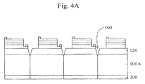
- FIG. 4A shows a wafer having LEDs formed thereon.
- Scribe lines 300 are formed on the wafer through the buffer layer 120 from the side having the LEDs (front scribing) to separate the LED chips.
- the scribe lines 300 are formed using, for example, a dry etching technique or mechanical scribing.
- the dry etching technique such as inductively coupled plasma (ICP) reactive ion beam etching (RIE) can form very narrow scribe lines on the buffer layer 120 and the substrate 100 A.
- ICP inductively coupled plasma
- RIE reactive ion beam etching
- FIG. 4B is an alternative method of forming the scribe lines in which the back side of the diode used.
- the scribe lines may also be formed by a diamond stylus, which requires a large spacing between the diode chips due to the size of the diamond stylus itself. Also, a dicing technique may be used to separate the chips.
- each diode may be packaged. Such package may also be coated with a reflective material to further enhance the light output.
- the present invention applies a simple and inexpensive light extraction process to the existing device fabrication process. According to this invention, adding just one more step of metallization after backside lapping and polishing allows a significant light output increase. With finer polishing using dry etching, in some cases, the light output can be as much as a factor of four without a substantial increase in production cost.
- the diode of the present invention improves light intensity of a diode such as an AlInGaN-based light emitting diode (LED) using a reflective coating.
- the reflective coating recovers those photons, which would otherwise be absorbed by the substrate or the lead frame in the LED package. This increases the total external quantum efficiency of the quantum well devices.
- This invention can be applied not only to the current commercially available blue, green, red and white LEDs but also to other LED devices. Using this technique, the light output was increased by as much as a factor of four as compared to conventional LED devices (without the reflective coating) without significantly sacrificing or changing other characteristics of the diode.
- the reflector and substrate polishing technique of the present invention can easily be applied to other types of diodes including red LEDs and laser diodes including VCSELs.
- red LEDs do not use GaN
- the substrate of the red LEDs may just as easily be polished and a reflective layer can easily be attached to the polished surface of the substrate, as described above.
- Such technique also recovers the photons to increase the light output of the diode. Similar technique is also applicable for laser diodes.
Landscapes
- Engineering & Computer Science (AREA)
- Microelectronics & Electronic Packaging (AREA)
- Power Engineering (AREA)
- Computer Hardware Design (AREA)
- Manufacturing & Machinery (AREA)
- Physics & Mathematics (AREA)
- Condensed Matter Physics & Semiconductors (AREA)
- General Physics & Mathematics (AREA)
- Led Devices (AREA)
Abstract
Description
Claims (19)
Priority Applications (3)
| Application Number | Priority Date | Filing Date | Title |
|---|---|---|---|
| US14/807,632 US9640713B2 (en) | 2001-07-17 | 2015-07-23 | Diode having high brightness and method thereof |
| US15/457,655 US10147841B2 (en) | 2001-07-17 | 2017-03-13 | Diode having high brightness and method thereof |
| US16/167,229 US10553744B2 (en) | 2001-07-17 | 2018-10-22 | Diode having high brightness and method thereof |
Applications Claiming Priority (6)
| Application Number | Priority Date | Filing Date | Title |
|---|---|---|---|
| US09/905,969 US7067849B2 (en) | 2001-07-17 | 2001-07-17 | Diode having high brightness and method thereof |
| US11/247,225 US7582912B2 (en) | 2001-07-17 | 2005-10-12 | Diode having high brightness and method thereof |
| US12/461,681 US7939849B2 (en) | 2001-07-17 | 2009-08-20 | Diode having high brightness and method thereof |
| US13/074,566 US8674386B2 (en) | 2001-07-17 | 2011-03-29 | Diode having high brightness and method thereof |
| US14/185,620 US9136424B2 (en) | 2001-07-17 | 2014-02-20 | Diode having high brightness and method thereof |
| US14/807,632 US9640713B2 (en) | 2001-07-17 | 2015-07-23 | Diode having high brightness and method thereof |
Related Parent Applications (1)
| Application Number | Title | Priority Date | Filing Date |
|---|---|---|---|
| US14/185,620 Continuation US9136424B2 (en) | 2001-07-17 | 2014-02-20 | Diode having high brightness and method thereof |
Related Child Applications (1)
| Application Number | Title | Priority Date | Filing Date |
|---|---|---|---|
| US15/457,655 Continuation US10147841B2 (en) | 2001-07-17 | 2017-03-13 | Diode having high brightness and method thereof |
Publications (2)
| Publication Number | Publication Date |
|---|---|
| US20150333217A1 US20150333217A1 (en) | 2015-11-19 |
| US9640713B2 true US9640713B2 (en) | 2017-05-02 |
Family
ID=25421760
Family Applications (8)
| Application Number | Title | Priority Date | Filing Date |
|---|---|---|---|
| US09/905,969 Expired - Lifetime US7067849B2 (en) | 2001-07-17 | 2001-07-17 | Diode having high brightness and method thereof |
| US11/247,225 Expired - Lifetime US7582912B2 (en) | 2001-07-17 | 2005-10-12 | Diode having high brightness and method thereof |
| US12/461,681 Expired - Lifetime US7939849B2 (en) | 2001-07-17 | 2009-08-20 | Diode having high brightness and method thereof |
| US13/074,566 Expired - Lifetime US8674386B2 (en) | 2001-07-17 | 2011-03-29 | Diode having high brightness and method thereof |
| US14/185,620 Expired - Fee Related US9136424B2 (en) | 2001-07-17 | 2014-02-20 | Diode having high brightness and method thereof |
| US14/807,632 Expired - Lifetime US9640713B2 (en) | 2001-07-17 | 2015-07-23 | Diode having high brightness and method thereof |
| US15/457,655 Expired - Fee Related US10147841B2 (en) | 2001-07-17 | 2017-03-13 | Diode having high brightness and method thereof |
| US16/167,229 Expired - Fee Related US10553744B2 (en) | 2001-07-17 | 2018-10-22 | Diode having high brightness and method thereof |
Family Applications Before (5)
| Application Number | Title | Priority Date | Filing Date |
|---|---|---|---|
| US09/905,969 Expired - Lifetime US7067849B2 (en) | 2001-07-17 | 2001-07-17 | Diode having high brightness and method thereof |
| US11/247,225 Expired - Lifetime US7582912B2 (en) | 2001-07-17 | 2005-10-12 | Diode having high brightness and method thereof |
| US12/461,681 Expired - Lifetime US7939849B2 (en) | 2001-07-17 | 2009-08-20 | Diode having high brightness and method thereof |
| US13/074,566 Expired - Lifetime US8674386B2 (en) | 2001-07-17 | 2011-03-29 | Diode having high brightness and method thereof |
| US14/185,620 Expired - Fee Related US9136424B2 (en) | 2001-07-17 | 2014-02-20 | Diode having high brightness and method thereof |
Family Applications After (2)
| Application Number | Title | Priority Date | Filing Date |
|---|---|---|---|
| US15/457,655 Expired - Fee Related US10147841B2 (en) | 2001-07-17 | 2017-03-13 | Diode having high brightness and method thereof |
| US16/167,229 Expired - Fee Related US10553744B2 (en) | 2001-07-17 | 2018-10-22 | Diode having high brightness and method thereof |
Country Status (2)
| Country | Link |
|---|---|
| US (8) | US7067849B2 (en) |
| WO (1) | WO2003015176A1 (en) |
Cited By (1)
| Publication number | Priority date | Publication date | Assignee | Title |
|---|---|---|---|---|
| US20170186906A1 (en) * | 2001-07-17 | 2017-06-29 | Lg Innotek Co., Ltd. | Diode having high brightness and method thereof |
Families Citing this family (271)
| Publication number | Priority date | Publication date | Assignee | Title |
|---|---|---|---|---|
| JP2002368263A (en) * | 2001-06-06 | 2002-12-20 | Toyoda Gosei Co Ltd | Iii nitride compound semiconductor light-emitting device |
| TWI294699B (en) * | 2006-01-27 | 2008-03-11 | Epistar Corp | Light emitting device and method of forming the same |
| US6949395B2 (en) | 2001-10-22 | 2005-09-27 | Oriol, Inc. | Method of making diode having reflective layer |
| US7148520B2 (en) | 2001-10-26 | 2006-12-12 | Lg Electronics Inc. | Diode having vertical structure and method of manufacturing the same |
| US7638346B2 (en) * | 2001-12-24 | 2009-12-29 | Crystal Is, Inc. | Nitride semiconductor heterostructures and related methods |
| US20060005763A1 (en) * | 2001-12-24 | 2006-01-12 | Crystal Is, Inc. | Method and apparatus for producing large, single-crystals of aluminum nitride |
| US8545629B2 (en) | 2001-12-24 | 2013-10-01 | Crystal Is, Inc. | Method and apparatus for producing large, single-crystals of aluminum nitride |
| US6818532B2 (en) * | 2002-04-09 | 2004-11-16 | Oriol, Inc. | Method of etching substrates |
| US8294172B2 (en) * | 2002-04-09 | 2012-10-23 | Lg Electronics Inc. | Method of fabricating vertical devices using a metal support film |
| US6841802B2 (en) | 2002-06-26 | 2005-01-11 | Oriol, Inc. | Thin film light emitting diode |
| WO2005122223A1 (en) * | 2004-06-11 | 2005-12-22 | Showa Denko K.K. | Production method of compound semiconductor device wafer |
| JP4837295B2 (en) * | 2005-03-02 | 2011-12-14 | 株式会社沖データ | Semiconductor device, LED device, LED head, and image forming apparatus |
| JP5281408B2 (en) * | 2005-12-02 | 2013-09-04 | クリスタル・イズ,インコーポレイテッド | Doped aluminum nitride crystal and method for producing the same |
| JP5191650B2 (en) * | 2005-12-16 | 2013-05-08 | シャープ株式会社 | Nitride semiconductor light emitting device and method for manufacturing nitride semiconductor light emitting device |
| KR100853241B1 (en) * | 2005-12-16 | 2008-08-20 | 샤프 가부시키가이샤 | Nitride Semiconductor Light Emitting Device and Method of Fabricating Nitride Semiconductor Laser Device |
| JP5004597B2 (en) * | 2006-03-06 | 2012-08-22 | シャープ株式会社 | Nitride semiconductor light emitting device and method for manufacturing nitride semiconductor light emitting device |
| JP5430826B2 (en) * | 2006-03-08 | 2014-03-05 | シャープ株式会社 | Nitride semiconductor laser device |
| US9034103B2 (en) * | 2006-03-30 | 2015-05-19 | Crystal Is, Inc. | Aluminum nitride bulk crystals having high transparency to ultraviolet light and methods of forming them |
| EP2007933B1 (en) * | 2006-03-30 | 2017-05-10 | Crystal Is, Inc. | Methods for controllable doping of aluminum nitride bulk crystals |
| JP4444304B2 (en) * | 2006-04-24 | 2010-03-31 | シャープ株式会社 | Nitride semiconductor light emitting device and method for manufacturing nitride semiconductor light emitting device |
| EP1887634A3 (en) * | 2006-08-11 | 2011-09-07 | OSRAM Opto Semiconductors GmbH | Semiconductor light emitting device |
| TW201448263A (en) | 2006-12-11 | 2014-12-16 | Univ California | Transparent light emitting diodes |
| US9771666B2 (en) | 2007-01-17 | 2017-09-26 | Crystal Is, Inc. | Defect reduction in seeded aluminum nitride crystal growth |
| US8323406B2 (en) * | 2007-01-17 | 2012-12-04 | Crystal Is, Inc. | Defect reduction in seeded aluminum nitride crystal growth |
| US9437430B2 (en) * | 2007-01-26 | 2016-09-06 | Crystal Is, Inc. | Thick pseudomorphic nitride epitaxial layers |
| US8080833B2 (en) | 2007-01-26 | 2011-12-20 | Crystal Is, Inc. | Thick pseudomorphic nitride epitaxial layers |
| JP2008244161A (en) * | 2007-03-27 | 2008-10-09 | Toyoda Gosei Co Ltd | Method for forming electrode of group iii nitride-based compound semiconductor light-emitting element |
| DE102007019776A1 (en) * | 2007-04-26 | 2008-10-30 | Osram Opto Semiconductors Gmbh | Optoelectronic component and method for producing a plurality of optoelectronic components |
| TWI343663B (en) * | 2007-05-15 | 2011-06-11 | Epistar Corp | Light emitting diode device and manufacturing method therof |
| US8088220B2 (en) | 2007-05-24 | 2012-01-03 | Crystal Is, Inc. | Deep-eutectic melt growth of nitride crystals |
| JP4310352B2 (en) * | 2007-06-05 | 2009-08-05 | シャープ株式会社 | Light emitting device and method for manufacturing light emitting device |
| JP5167974B2 (en) * | 2008-06-16 | 2013-03-21 | 豊田合成株式会社 | Group III nitride compound semiconductor light emitting device and method of manufacturing the same |
| US20100019222A1 (en) * | 2008-07-25 | 2010-01-28 | High Power Opto.Inc. | Low-temperature led chip metal bonding layer |
| US9509313B2 (en) | 2009-04-14 | 2016-11-29 | Monolithic 3D Inc. | 3D semiconductor device |
| US8395191B2 (en) | 2009-10-12 | 2013-03-12 | Monolithic 3D Inc. | Semiconductor device and structure |
| US9577642B2 (en) | 2009-04-14 | 2017-02-21 | Monolithic 3D Inc. | Method to form a 3D semiconductor device |
| US8427200B2 (en) | 2009-04-14 | 2013-04-23 | Monolithic 3D Inc. | 3D semiconductor device |
| US8362800B2 (en) | 2010-10-13 | 2013-01-29 | Monolithic 3D Inc. | 3D semiconductor device including field repairable logics |
| US8362482B2 (en) | 2009-04-14 | 2013-01-29 | Monolithic 3D Inc. | Semiconductor device and structure |
| US9711407B2 (en) * | 2009-04-14 | 2017-07-18 | Monolithic 3D Inc. | Method of manufacturing a three dimensional integrated circuit by transfer of a mono-crystalline layer |
| US7986042B2 (en) | 2009-04-14 | 2011-07-26 | Monolithic 3D Inc. | Method for fabrication of a semiconductor device and structure |
| US8405420B2 (en) * | 2009-04-14 | 2013-03-26 | Monolithic 3D Inc. | System comprising a semiconductor device and structure |
| US8058137B1 (en) | 2009-04-14 | 2011-11-15 | Monolithic 3D Inc. | Method for fabrication of a semiconductor device and structure |
| US8754533B2 (en) * | 2009-04-14 | 2014-06-17 | Monolithic 3D Inc. | Monolithic three-dimensional semiconductor device and structure |
| US8373439B2 (en) | 2009-04-14 | 2013-02-12 | Monolithic 3D Inc. | 3D semiconductor device |
| US8384426B2 (en) * | 2009-04-14 | 2013-02-26 | Monolithic 3D Inc. | Semiconductor device and structure |
| US8669778B1 (en) | 2009-04-14 | 2014-03-11 | Monolithic 3D Inc. | Method for design and manufacturing of a 3D semiconductor device |
| US8378715B2 (en) | 2009-04-14 | 2013-02-19 | Monolithic 3D Inc. | Method to construct systems |
| JP2012524964A (en) * | 2009-04-24 | 2012-10-18 | コーニンクレッカ フィリップス エレクトロニクス エヌ ヴィ | Illumination system including beam shape adjusting element |
| US8581349B1 (en) | 2011-05-02 | 2013-11-12 | Monolithic 3D Inc. | 3D memory semiconductor device and structure |
| US8536023B2 (en) | 2010-11-22 | 2013-09-17 | Monolithic 3D Inc. | Method of manufacturing a semiconductor device and structure |
| US10910364B2 (en) | 2009-10-12 | 2021-02-02 | Monolitaic 3D Inc. | 3D semiconductor device |
| US11984445B2 (en) | 2009-10-12 | 2024-05-14 | Monolithic 3D Inc. | 3D semiconductor devices and structures with metal layers |
| US8294159B2 (en) | 2009-10-12 | 2012-10-23 | Monolithic 3D Inc. | Method for fabrication of a semiconductor device and structure |
| US9099424B1 (en) | 2012-08-10 | 2015-08-04 | Monolithic 3D Inc. | Semiconductor system, device and structure with heat removal |
| US10366970B2 (en) | 2009-10-12 | 2019-07-30 | Monolithic 3D Inc. | 3D semiconductor device and structure |
| US8742476B1 (en) | 2012-11-27 | 2014-06-03 | Monolithic 3D Inc. | Semiconductor device and structure |
| US10157909B2 (en) | 2009-10-12 | 2018-12-18 | Monolithic 3D Inc. | 3D semiconductor device and structure |
| US11018133B2 (en) | 2009-10-12 | 2021-05-25 | Monolithic 3D Inc. | 3D integrated circuit |
| US8476145B2 (en) | 2010-10-13 | 2013-07-02 | Monolithic 3D Inc. | Method of fabricating a semiconductor device and structure |
| US10354995B2 (en) | 2009-10-12 | 2019-07-16 | Monolithic 3D Inc. | Semiconductor memory device and structure |
| US10043781B2 (en) | 2009-10-12 | 2018-08-07 | Monolithic 3D Inc. | 3D semiconductor device and structure |
| US12027518B1 (en) | 2009-10-12 | 2024-07-02 | Monolithic 3D Inc. | 3D semiconductor devices and structures with metal layers |
| US10388863B2 (en) | 2009-10-12 | 2019-08-20 | Monolithic 3D Inc. | 3D memory device and structure |
| US11374118B2 (en) | 2009-10-12 | 2022-06-28 | Monolithic 3D Inc. | Method to form a 3D integrated circuit |
| US8450804B2 (en) | 2011-03-06 | 2013-05-28 | Monolithic 3D Inc. | Semiconductor device and structure for heat removal |
| TWI531088B (en) * | 2009-11-13 | 2016-04-21 | 首爾偉傲世有限公司 | Light emitting diode chip having distributed bragg reflector |
| US8963178B2 (en) | 2009-11-13 | 2015-02-24 | Seoul Viosys Co., Ltd. | Light emitting diode chip having distributed bragg reflector and method of fabricating the same |
| JP5343018B2 (en) * | 2010-02-08 | 2013-11-13 | 昭和電工株式会社 | LIGHT EMITTING DIODE, MANUFACTURING METHOD THEREOF, AND LIGHT EMITTING DIODE LAMP |
| US8461035B1 (en) | 2010-09-30 | 2013-06-11 | Monolithic 3D Inc. | Method for fabrication of a semiconductor device and structure |
| US8492886B2 (en) | 2010-02-16 | 2013-07-23 | Monolithic 3D Inc | 3D integrated circuit with logic |
| US8541819B1 (en) | 2010-12-09 | 2013-09-24 | Monolithic 3D Inc. | Semiconductor device and structure |
| US8373230B1 (en) | 2010-10-13 | 2013-02-12 | Monolithic 3D Inc. | Method for fabrication of a semiconductor device and structure |
| US9099526B2 (en) | 2010-02-16 | 2015-08-04 | Monolithic 3D Inc. | Integrated circuit device and structure |
| US8026521B1 (en) | 2010-10-11 | 2011-09-27 | Monolithic 3D Inc. | Semiconductor device and structure |
| JP5414627B2 (en) * | 2010-06-07 | 2014-02-12 | 株式会社東芝 | Semiconductor light emitting device and manufacturing method thereof |
| CN101882661B (en) * | 2010-06-28 | 2013-04-03 | 天津爱瓦顿科技有限公司 | LED microcavity structure suitable for special lighting |
| JP5806734B2 (en) | 2010-06-30 | 2015-11-10 | クリスタル アイエス, インコーポレーテッドCrystal Is, Inc. | Large single crystal growth of aluminum nitride by thermal gradient control |
| US9293678B2 (en) * | 2010-07-15 | 2016-03-22 | Micron Technology, Inc. | Solid-state light emitters having substrates with thermal and electrical conductivity enhancements and method of manufacture |
| US9219005B2 (en) | 2011-06-28 | 2015-12-22 | Monolithic 3D Inc. | Semiconductor system and device |
| US9953925B2 (en) | 2011-06-28 | 2018-04-24 | Monolithic 3D Inc. | Semiconductor system and device |
| US10217667B2 (en) | 2011-06-28 | 2019-02-26 | Monolithic 3D Inc. | 3D semiconductor device, fabrication method and system |
| US8642416B2 (en) | 2010-07-30 | 2014-02-04 | Monolithic 3D Inc. | Method of forming three dimensional integrated circuit devices using layer transfer technique |
| US8901613B2 (en) | 2011-03-06 | 2014-12-02 | Monolithic 3D Inc. | Semiconductor device and structure for heat removal |
| US9070851B2 (en) | 2010-09-24 | 2015-06-30 | Seoul Semiconductor Co., Ltd. | Wafer-level light emitting diode package and method of fabricating the same |
| US8163581B1 (en) | 2010-10-13 | 2012-04-24 | Monolith IC 3D | Semiconductor and optoelectronic devices |
| US10497713B2 (en) | 2010-11-18 | 2019-12-03 | Monolithic 3D Inc. | 3D semiconductor memory device and structure |
| US8273610B2 (en) | 2010-11-18 | 2012-09-25 | Monolithic 3D Inc. | Method of constructing a semiconductor device and structure |
| US11482440B2 (en) | 2010-12-16 | 2022-10-25 | Monolithic 3D Inc. | 3D semiconductor device and structure with a built-in test circuit for repairing faulty circuits |
| US11227897B2 (en) | 2010-10-11 | 2022-01-18 | Monolithic 3D Inc. | Method for producing a 3D semiconductor memory device and structure |
| US11018191B1 (en) | 2010-10-11 | 2021-05-25 | Monolithic 3D Inc. | 3D semiconductor device and structure |
| US11600667B1 (en) | 2010-10-11 | 2023-03-07 | Monolithic 3D Inc. | Method to produce 3D semiconductor devices and structures with memory |
| US8114757B1 (en) | 2010-10-11 | 2012-02-14 | Monolithic 3D Inc. | Semiconductor device and structure |
| US11469271B2 (en) | 2010-10-11 | 2022-10-11 | Monolithic 3D Inc. | Method to produce 3D semiconductor devices and structures with memory |
| US10290682B2 (en) | 2010-10-11 | 2019-05-14 | Monolithic 3D Inc. | 3D IC semiconductor device and structure with stacked memory |
| US10896931B1 (en) | 2010-10-11 | 2021-01-19 | Monolithic 3D Inc. | 3D semiconductor device and structure |
| US11257867B1 (en) | 2010-10-11 | 2022-02-22 | Monolithic 3D Inc. | 3D semiconductor device and structure with oxide bonds |
| US11158674B2 (en) | 2010-10-11 | 2021-10-26 | Monolithic 3D Inc. | Method to produce a 3D semiconductor device and structure |
| US11315980B1 (en) | 2010-10-11 | 2022-04-26 | Monolithic 3D Inc. | 3D semiconductor device and structure with transistors |
| US11024673B1 (en) | 2010-10-11 | 2021-06-01 | Monolithic 3D Inc. | 3D semiconductor device and structure |
| US20120091474A1 (en) * | 2010-10-13 | 2012-04-19 | NuPGA Corporation | Novel semiconductor and optoelectronic devices |
| US10943934B2 (en) | 2010-10-13 | 2021-03-09 | Monolithic 3D Inc. | Multilevel semiconductor device and structure |
| US11133344B2 (en) | 2010-10-13 | 2021-09-28 | Monolithic 3D Inc. | Multilevel semiconductor device and structure with image sensors |
| US9197804B1 (en) | 2011-10-14 | 2015-11-24 | Monolithic 3D Inc. | Semiconductor and optoelectronic devices |
| US12080743B2 (en) | 2010-10-13 | 2024-09-03 | Monolithic 3D Inc. | Multilevel semiconductor device and structure with image sensors and wafer bonding |
| US11437368B2 (en) | 2010-10-13 | 2022-09-06 | Monolithic 3D Inc. | Multilevel semiconductor device and structure with oxide bonding |
| US10679977B2 (en) | 2010-10-13 | 2020-06-09 | Monolithic 3D Inc. | 3D microdisplay device and structure |
| US10998374B1 (en) | 2010-10-13 | 2021-05-04 | Monolithic 3D Inc. | Multilevel semiconductor device and structure |
| US11984438B2 (en) | 2010-10-13 | 2024-05-14 | Monolithic 3D Inc. | Multilevel semiconductor device and structure with oxide bonding |
| US11404466B2 (en) | 2010-10-13 | 2022-08-02 | Monolithic 3D Inc. | Multilevel semiconductor device and structure with image sensors |
| US11869915B2 (en) | 2010-10-13 | 2024-01-09 | Monolithic 3D Inc. | Multilevel semiconductor device and structure with image sensors and wafer bonding |
| US11163112B2 (en) | 2010-10-13 | 2021-11-02 | Monolithic 3D Inc. | Multilevel semiconductor device and structure with electromagnetic modulators |
| US11063071B1 (en) | 2010-10-13 | 2021-07-13 | Monolithic 3D Inc. | Multilevel semiconductor device and structure with waveguides |
| US8379458B1 (en) | 2010-10-13 | 2013-02-19 | Monolithic 3D Inc. | Semiconductor device and structure |
| US11164898B2 (en) | 2010-10-13 | 2021-11-02 | Monolithic 3D Inc. | Multilevel semiconductor device and structure |
| US10833108B2 (en) | 2010-10-13 | 2020-11-10 | Monolithic 3D Inc. | 3D microdisplay device and structure |
| US11855100B2 (en) | 2010-10-13 | 2023-12-26 | Monolithic 3D Inc. | Multilevel semiconductor device and structure with oxide bonding |
| US12094892B2 (en) | 2010-10-13 | 2024-09-17 | Monolithic 3D Inc. | 3D micro display device and structure |
| US10978501B1 (en) | 2010-10-13 | 2021-04-13 | Monolithic 3D Inc. | Multilevel semiconductor device and structure with waveguides |
| US11694922B2 (en) | 2010-10-13 | 2023-07-04 | Monolithic 3D Inc. | Multilevel semiconductor device and structure with oxide bonding |
| US11043523B1 (en) | 2010-10-13 | 2021-06-22 | Monolithic 3D Inc. | Multilevel semiconductor device and structure with image sensors |
| US11929372B2 (en) | 2010-10-13 | 2024-03-12 | Monolithic 3D Inc. | Multilevel semiconductor device and structure with image sensors and wafer bonding |
| US11327227B2 (en) | 2010-10-13 | 2022-05-10 | Monolithic 3D Inc. | Multilevel semiconductor device and structure with electromagnetic modulators |
| US11605663B2 (en) | 2010-10-13 | 2023-03-14 | Monolithic 3D Inc. | Multilevel semiconductor device and structure with image sensors and wafer bonding |
| US11855114B2 (en) | 2010-10-13 | 2023-12-26 | Monolithic 3D Inc. | Multilevel semiconductor device and structure with image sensors and wafer bonding |
| US11610802B2 (en) | 2010-11-18 | 2023-03-21 | Monolithic 3D Inc. | Method for producing a 3D semiconductor device and structure with single crystal transistors and metal gate electrodes |
| US11164770B1 (en) | 2010-11-18 | 2021-11-02 | Monolithic 3D Inc. | Method for producing a 3D semiconductor memory device and structure |
| US11482438B2 (en) | 2010-11-18 | 2022-10-25 | Monolithic 3D Inc. | Methods for producing a 3D semiconductor memory device and structure |
| US11018042B1 (en) | 2010-11-18 | 2021-05-25 | Monolithic 3D Inc. | 3D semiconductor memory device and structure |
| US12100611B2 (en) | 2010-11-18 | 2024-09-24 | Monolithic 3D Inc. | Methods for producing a 3D semiconductor device and structure with memory cells and multiple metal layers |
| US11495484B2 (en) | 2010-11-18 | 2022-11-08 | Monolithic 3D Inc. | 3D semiconductor devices and structures with at least two single-crystal layers |
| US11901210B2 (en) | 2010-11-18 | 2024-02-13 | Monolithic 3D Inc. | 3D semiconductor device and structure with memory |
| US11569117B2 (en) | 2010-11-18 | 2023-01-31 | Monolithic 3D Inc. | 3D semiconductor device and structure with single-crystal layers |
| US11615977B2 (en) | 2010-11-18 | 2023-03-28 | Monolithic 3D Inc. | 3D semiconductor memory device and structure |
| US11004719B1 (en) | 2010-11-18 | 2021-05-11 | Monolithic 3D Inc. | Methods for producing a 3D semiconductor memory device and structure |
| US11923230B1 (en) | 2010-11-18 | 2024-03-05 | Monolithic 3D Inc. | 3D semiconductor device and structure with bonding |
| US11854857B1 (en) | 2010-11-18 | 2023-12-26 | Monolithic 3D Inc. | Methods for producing a 3D semiconductor device and structure with memory cells and multiple metal layers |
| US11107721B2 (en) | 2010-11-18 | 2021-08-31 | Monolithic 3D Inc. | 3D semiconductor device and structure with NAND logic |
| US11862503B2 (en) | 2010-11-18 | 2024-01-02 | Monolithic 3D Inc. | Method for producing a 3D semiconductor device and structure with memory cells and multiple metal layers |
| US11521888B2 (en) | 2010-11-18 | 2022-12-06 | Monolithic 3D Inc. | 3D semiconductor device and structure with high-k metal gate transistors |
| US11508605B2 (en) | 2010-11-18 | 2022-11-22 | Monolithic 3D Inc. | 3D semiconductor memory device and structure |
| US11784082B2 (en) | 2010-11-18 | 2023-10-10 | Monolithic 3D Inc. | 3D semiconductor device and structure with bonding |
| US11355380B2 (en) | 2010-11-18 | 2022-06-07 | Monolithic 3D Inc. | Methods for producing 3D semiconductor memory device and structure utilizing alignment marks |
| US11211279B2 (en) | 2010-11-18 | 2021-12-28 | Monolithic 3D Inc. | Method for processing a 3D integrated circuit and structure |
| US11443971B2 (en) | 2010-11-18 | 2022-09-13 | Monolithic 3D Inc. | 3D semiconductor device and structure with memory |
| US11121021B2 (en) | 2010-11-18 | 2021-09-14 | Monolithic 3D Inc. | 3D semiconductor device and structure |
| US11735462B2 (en) | 2010-11-18 | 2023-08-22 | Monolithic 3D Inc. | 3D semiconductor device and structure with single-crystal layers |
| US12068187B2 (en) | 2010-11-18 | 2024-08-20 | Monolithic 3D Inc. | 3D semiconductor device and structure with bonding and DRAM memory cells |
| US11355381B2 (en) | 2010-11-18 | 2022-06-07 | Monolithic 3D Inc. | 3D semiconductor memory device and structure |
| US11804396B2 (en) | 2010-11-18 | 2023-10-31 | Monolithic 3D Inc. | Methods for producing a 3D semiconductor device and structure with memory cells and multiple metal layers |
| US11094576B1 (en) | 2010-11-18 | 2021-08-17 | Monolithic 3D Inc. | Methods for producing a 3D semiconductor memory device and structure |
| US12033884B2 (en) | 2010-11-18 | 2024-07-09 | Monolithic 3D Inc. | Methods for producing a 3D semiconductor device and structure with memory cells and multiple metal layers |
| US11031275B2 (en) | 2010-11-18 | 2021-06-08 | Monolithic 3D Inc. | 3D semiconductor device and structure with memory |
| US11482439B2 (en) | 2010-11-18 | 2022-10-25 | Monolithic 3D Inc. | Methods for producing a 3D semiconductor memory device comprising charge trap junction-less transistors |
| CN102593287B (en) * | 2011-01-10 | 2015-07-08 | 展晶科技(深圳)有限公司 | LED crystal grain and manufacturing method thereof as well as LED packaging structure |
| US8975670B2 (en) | 2011-03-06 | 2015-03-10 | Monolithic 3D Inc. | Semiconductor device and structure for heat removal |
| US10388568B2 (en) | 2011-06-28 | 2019-08-20 | Monolithic 3D Inc. | 3D semiconductor device and system |
| US8962359B2 (en) | 2011-07-19 | 2015-02-24 | Crystal Is, Inc. | Photon extraction from nitride ultraviolet light-emitting devices |
| US8687399B2 (en) | 2011-10-02 | 2014-04-01 | Monolithic 3D Inc. | Semiconductor device and structure |
| US9029173B2 (en) | 2011-10-18 | 2015-05-12 | Monolithic 3D Inc. | Method for fabrication of a semiconductor device and structure |
| KR20130049568A (en) * | 2011-11-04 | 2013-05-14 | 삼성전자주식회사 | Light emitting device and manufacturing method thereof |
| TW201324705A (en) * | 2011-12-08 | 2013-06-16 | Genesis Photonics Inc | Electronic device |
| KR20130078281A (en) * | 2011-12-30 | 2013-07-10 | 삼성전자주식회사 | Nitride based semiconductor device and method for manufacturing the same |
| US9000464B2 (en) * | 2012-03-01 | 2015-04-07 | Design Express Limited | Semiconductor structure for substrate separation and method for manufacturing the same |
| US9000557B2 (en) | 2012-03-17 | 2015-04-07 | Zvi Or-Bach | Semiconductor device and structure |
| US8575657B2 (en) | 2012-03-20 | 2013-11-05 | Northrop Grumman Systems Corporation | Direct growth of diamond in backside vias for GaN HEMT devices |
| US11694944B1 (en) | 2012-04-09 | 2023-07-04 | Monolithic 3D Inc. | 3D semiconductor device and structure with metal layers and a connective path |
| US11164811B2 (en) | 2012-04-09 | 2021-11-02 | Monolithic 3D Inc. | 3D semiconductor device with isolation layers and oxide-to-oxide bonding |
| US11476181B1 (en) | 2012-04-09 | 2022-10-18 | Monolithic 3D Inc. | 3D semiconductor device and structure with metal layers |
| US10600888B2 (en) | 2012-04-09 | 2020-03-24 | Monolithic 3D Inc. | 3D semiconductor device |
| US11088050B2 (en) | 2012-04-09 | 2021-08-10 | Monolithic 3D Inc. | 3D semiconductor device with isolation layers |
| US11616004B1 (en) | 2012-04-09 | 2023-03-28 | Monolithic 3D Inc. | 3D semiconductor device and structure with metal layers and a connective path |
| US11881443B2 (en) | 2012-04-09 | 2024-01-23 | Monolithic 3D Inc. | 3D semiconductor device and structure with metal layers and a connective path |
| US11594473B2 (en) | 2012-04-09 | 2023-02-28 | Monolithic 3D Inc. | 3D semiconductor device and structure with metal layers and a connective path |
| US11410912B2 (en) | 2012-04-09 | 2022-08-09 | Monolithic 3D Inc. | 3D semiconductor device with vias and isolation layers |
| US8557632B1 (en) | 2012-04-09 | 2013-10-15 | Monolithic 3D Inc. | Method for fabrication of a semiconductor device and structure |
| US11735501B1 (en) | 2012-04-09 | 2023-08-22 | Monolithic 3D Inc. | 3D semiconductor device and structure with metal layers and a connective path |
| CN103794691B (en) * | 2012-10-30 | 2018-03-20 | 首尔伟傲世有限公司 | Light emitting diode and its manufacture method |
| US8686428B1 (en) | 2012-11-16 | 2014-04-01 | Monolithic 3D Inc. | Semiconductor device and structure |
| US8574929B1 (en) | 2012-11-16 | 2013-11-05 | Monolithic 3D Inc. | Method to form a 3D semiconductor device and structure |
| US8674470B1 (en) | 2012-12-22 | 2014-03-18 | Monolithic 3D Inc. | Semiconductor device and structure |
| US11967583B2 (en) | 2012-12-22 | 2024-04-23 | Monolithic 3D Inc. | 3D semiconductor device and structure with metal layers |
| US11217565B2 (en) | 2012-12-22 | 2022-01-04 | Monolithic 3D Inc. | Method to form a 3D semiconductor device and structure |
| US11784169B2 (en) | 2012-12-22 | 2023-10-10 | Monolithic 3D Inc. | 3D semiconductor device and structure with metal layers |
| US12051674B2 (en) | 2012-12-22 | 2024-07-30 | Monolithic 3D Inc. | 3D semiconductor device and structure with metal layers |
| US11063024B1 (en) | 2012-12-22 | 2021-07-13 | Monlithic 3D Inc. | Method to form a 3D semiconductor device and structure |
| US11916045B2 (en) | 2012-12-22 | 2024-02-27 | Monolithic 3D Inc. | 3D semiconductor device and structure with metal layers |
| US11961827B1 (en) | 2012-12-22 | 2024-04-16 | Monolithic 3D Inc. | 3D semiconductor device and structure with metal layers |
| US11309292B2 (en) | 2012-12-22 | 2022-04-19 | Monolithic 3D Inc. | 3D semiconductor device and structure with metal layers |
| US11018116B2 (en) | 2012-12-22 | 2021-05-25 | Monolithic 3D Inc. | Method to form a 3D semiconductor device and structure |
| US8796693B2 (en) * | 2012-12-26 | 2014-08-05 | Seoul Semiconductor Co., Ltd. | Successive ionic layer adsorption and reaction process for depositing epitaxial ZnO on III-nitride-based light emitting diode and light emitting diode including epitaxial ZnO |
| US11177140B2 (en) | 2012-12-29 | 2021-11-16 | Monolithic 3D Inc. | 3D semiconductor device and structure |
| US10651054B2 (en) | 2012-12-29 | 2020-05-12 | Monolithic 3D Inc. | 3D semiconductor device and structure |
| US11004694B1 (en) | 2012-12-29 | 2021-05-11 | Monolithic 3D Inc. | 3D semiconductor device and structure |
| US10600657B2 (en) | 2012-12-29 | 2020-03-24 | Monolithic 3D Inc | 3D semiconductor device and structure |
| US10892169B2 (en) | 2012-12-29 | 2021-01-12 | Monolithic 3D Inc. | 3D semiconductor device and structure |
| US10115663B2 (en) | 2012-12-29 | 2018-10-30 | Monolithic 3D Inc. | 3D semiconductor device and structure |
| US10903089B1 (en) | 2012-12-29 | 2021-01-26 | Monolithic 3D Inc. | 3D semiconductor device and structure |
| US9871034B1 (en) | 2012-12-29 | 2018-01-16 | Monolithic 3D Inc. | Semiconductor device and structure |
| US11430668B2 (en) | 2012-12-29 | 2022-08-30 | Monolithic 3D Inc. | 3D semiconductor device and structure with bonding |
| US9385058B1 (en) | 2012-12-29 | 2016-07-05 | Monolithic 3D Inc. | Semiconductor device and structure |
| US11087995B1 (en) | 2012-12-29 | 2021-08-10 | Monolithic 3D Inc. | 3D semiconductor device and structure |
| US11430667B2 (en) | 2012-12-29 | 2022-08-30 | Monolithic 3D Inc. | 3D semiconductor device and structure with bonding |
| US9490131B2 (en) * | 2013-01-24 | 2016-11-08 | Koninklijke Philips N.V. | Control of P-contact resistance in a semiconductor light emitting device |
| US11869965B2 (en) | 2013-03-11 | 2024-01-09 | Monolithic 3D Inc. | 3D semiconductor device and structure with metal layers and memory cells |
| US8902663B1 (en) | 2013-03-11 | 2014-12-02 | Monolithic 3D Inc. | Method of maintaining a memory state |
| US12094965B2 (en) | 2013-03-11 | 2024-09-17 | Monolithic 3D Inc. | 3D semiconductor device and structure with metal layers and memory cells |
| US11935949B1 (en) | 2013-03-11 | 2024-03-19 | Monolithic 3D Inc. | 3D semiconductor device and structure with metal layers and memory cells |
| US10325651B2 (en) | 2013-03-11 | 2019-06-18 | Monolithic 3D Inc. | 3D semiconductor device with stacked memory |
| US8994404B1 (en) | 2013-03-12 | 2015-03-31 | Monolithic 3D Inc. | Semiconductor device and structure |
| US11398569B2 (en) | 2013-03-12 | 2022-07-26 | Monolithic 3D Inc. | 3D semiconductor device and structure |
| US10840239B2 (en) | 2014-08-26 | 2020-11-17 | Monolithic 3D Inc. | 3D semiconductor device and structure |
| US11088130B2 (en) | 2014-01-28 | 2021-08-10 | Monolithic 3D Inc. | 3D semiconductor device and structure |
| US11923374B2 (en) | 2013-03-12 | 2024-03-05 | Monolithic 3D Inc. | 3D semiconductor device and structure with metal layers |
| US12100646B2 (en) | 2013-03-12 | 2024-09-24 | Monolithic 3D Inc. | 3D semiconductor device and structure with metal layers |
| US9117749B1 (en) | 2013-03-15 | 2015-08-25 | Monolithic 3D Inc. | Semiconductor device and structure |
| US10224279B2 (en) | 2013-03-15 | 2019-03-05 | Monolithic 3D Inc. | Semiconductor device and structure |
| US20150280057A1 (en) | 2013-03-15 | 2015-10-01 | James R. Grandusky | Methods of forming planar contacts to pseudomorphic electronic and optoelectronic devices |
| US11030371B2 (en) | 2013-04-15 | 2021-06-08 | Monolithic 3D Inc. | Automation for monolithic 3D devices |
| US11574109B1 (en) | 2013-04-15 | 2023-02-07 | Monolithic 3D Inc | Automation methods for 3D integrated circuits and devices |
| US11720736B2 (en) | 2013-04-15 | 2023-08-08 | Monolithic 3D Inc. | Automation methods for 3D integrated circuits and devices |
| US9021414B1 (en) | 2013-04-15 | 2015-04-28 | Monolithic 3D Inc. | Automation for monolithic 3D devices |
| US11270055B1 (en) | 2013-04-15 | 2022-03-08 | Monolithic 3D Inc. | Automation for monolithic 3D devices |
| US11341309B1 (en) | 2013-04-15 | 2022-05-24 | Monolithic 3D Inc. | Automation for monolithic 3D devices |
| US11487928B2 (en) | 2013-04-15 | 2022-11-01 | Monolithic 3D Inc. | Automation for monolithic 3D devices |
| US11031394B1 (en) | 2014-01-28 | 2021-06-08 | Monolithic 3D Inc. | 3D semiconductor device and structure |
| US12094829B2 (en) | 2014-01-28 | 2024-09-17 | Monolithic 3D Inc. | 3D semiconductor device and structure |
| US10297586B2 (en) | 2015-03-09 | 2019-05-21 | Monolithic 3D Inc. | Methods for processing a 3D semiconductor device |
| US11107808B1 (en) | 2014-01-28 | 2021-08-31 | Monolithic 3D Inc. | 3D semiconductor device and structure |
| FR3023061B1 (en) * | 2014-06-27 | 2017-12-15 | Commissariat Energie Atomique | MESA STRUCTURE DIODE WITH SUBSTANTIALLY PLANE CONTACT SURFACE |
| WO2016006298A1 (en) * | 2014-07-07 | 2016-01-14 | ソニー株式会社 | Semiconductor optical device |
| US10245313B2 (en) * | 2014-10-24 | 2019-04-02 | Versitech Limited | DNA motif compounds and methods for inducing specific antibodies and cellular immunity |
| US11056468B1 (en) | 2015-04-19 | 2021-07-06 | Monolithic 3D Inc. | 3D semiconductor device and structure |
| US10381328B2 (en) | 2015-04-19 | 2019-08-13 | Monolithic 3D Inc. | Semiconductor device and structure |
| US10825779B2 (en) | 2015-04-19 | 2020-11-03 | Monolithic 3D Inc. | 3D semiconductor device and structure |
| US11011507B1 (en) | 2015-04-19 | 2021-05-18 | Monolithic 3D Inc. | 3D semiconductor device and structure |
| WO2016202039A1 (en) * | 2015-06-17 | 2016-12-22 | 厦门市三安光电科技有限公司 | Light emitting diode and preparation method thereof |
| US11956952B2 (en) | 2015-08-23 | 2024-04-09 | Monolithic 3D Inc. | Semiconductor memory device and structure |
| US11114427B2 (en) | 2015-11-07 | 2021-09-07 | Monolithic 3D Inc. | 3D semiconductor processor and memory device and structure |
| US12100658B2 (en) | 2015-09-21 | 2024-09-24 | Monolithic 3D Inc. | Method to produce a 3D multilayer semiconductor device and structure |
| US11937422B2 (en) | 2015-11-07 | 2024-03-19 | Monolithic 3D Inc. | Semiconductor memory device and structure |
| DE112016004265T5 (en) | 2015-09-21 | 2018-06-07 | Monolithic 3D Inc. | 3D SEMICONDUCTOR DEVICE AND STRUCTURE |
| US11978731B2 (en) | 2015-09-21 | 2024-05-07 | Monolithic 3D Inc. | Method to produce a multi-level semiconductor memory device and structure |
| US10522225B1 (en) | 2015-10-02 | 2019-12-31 | Monolithic 3D Inc. | Semiconductor device with non-volatile memory |
| KR102471102B1 (en) | 2015-10-23 | 2022-11-25 | 서울바이오시스 주식회사 | Light emitting diode chip having distributed bragg reflector |
| US12035531B2 (en) | 2015-10-24 | 2024-07-09 | Monolithic 3D Inc. | 3D semiconductor device and structure with logic and memory |
| US12120880B1 (en) | 2015-10-24 | 2024-10-15 | Monolithic 3D Inc. | 3D semiconductor device and structure with logic and memory |
| US11991884B1 (en) | 2015-10-24 | 2024-05-21 | Monolithic 3D Inc. | 3D semiconductor device and structure with logic and memory |
| US10418369B2 (en) | 2015-10-24 | 2019-09-17 | Monolithic 3D Inc. | Multi-level semiconductor memory device and structure |
| US11296115B1 (en) | 2015-10-24 | 2022-04-05 | Monolithic 3D Inc. | 3D semiconductor device and structure |
| US11114464B2 (en) | 2015-10-24 | 2021-09-07 | Monolithic 3D Inc. | 3D semiconductor device and structure |
| US10847540B2 (en) | 2015-10-24 | 2020-11-24 | Monolithic 3D Inc. | 3D semiconductor memory device and structure |
| US12016181B2 (en) | 2015-10-24 | 2024-06-18 | Monolithic 3D Inc. | 3D semiconductor device and structure with logic and memory |
| US20170186919A1 (en) * | 2015-12-29 | 2017-06-29 | Light Share, LLC | Optoelectronic Semiconductor Devices with Enhanced Light Output |
| CN105514232B (en) * | 2016-01-08 | 2018-04-24 | 华灿光电股份有限公司 | A kind of production method of LED epitaxial slice, light emitting diode and epitaxial wafer |
| CN205944139U (en) | 2016-03-30 | 2017-02-08 | 首尔伟傲世有限公司 | Ultraviolet ray light -emitting diode spare and contain this emitting diode module |
| US10026863B2 (en) * | 2016-07-13 | 2018-07-17 | Dpix, Llc | Method of manufacturing a sensor array |
| US11251149B2 (en) | 2016-10-10 | 2022-02-15 | Monolithic 3D Inc. | 3D memory device and structure |
| US11930648B1 (en) | 2016-10-10 | 2024-03-12 | Monolithic 3D Inc. | 3D memory devices and structures with metal layers |
| US11711928B2 (en) | 2016-10-10 | 2023-07-25 | Monolithic 3D Inc. | 3D memory devices and structures with control circuits |
| US11329059B1 (en) | 2016-10-10 | 2022-05-10 | Monolithic 3D Inc. | 3D memory devices and structures with thinned single crystal substrates |
| US11812620B2 (en) | 2016-10-10 | 2023-11-07 | Monolithic 3D Inc. | 3D DRAM memory devices and structures with control circuits |
| US11869591B2 (en) | 2016-10-10 | 2024-01-09 | Monolithic 3D Inc. | 3D memory devices and structures with control circuits |
| GB201716419D0 (en) | 2017-10-06 | 2017-11-22 | Univ Central Lancashire | Solid composition |
| JP6822429B2 (en) * | 2018-02-19 | 2021-01-27 | 日亜化学工業株式会社 | Light emitting element |
| DE102018111954B4 (en) * | 2018-05-17 | 2022-02-24 | OSRAM Opto Semiconductors Gesellschaft mit beschränkter Haftung | METHOD OF MANUFACTURING A SEMICONDUCTOR DEVICE WITH INSULATING SUBSTRATE AND A SEMICONDUCTOR DEVICE WITH INSULATING SUBSTRATE AND OPTOELECTRONIC DEVICE COMPRISING THESE |
| US11158652B1 (en) | 2019-04-08 | 2021-10-26 | Monolithic 3D Inc. | 3D memory semiconductor devices and structures |
| US11296106B2 (en) | 2019-04-08 | 2022-04-05 | Monolithic 3D Inc. | 3D memory semiconductor devices and structures |
| US11763864B2 (en) | 2019-04-08 | 2023-09-19 | Monolithic 3D Inc. | 3D memory semiconductor devices and structures with bit-line pillars |
| US11018156B2 (en) | 2019-04-08 | 2021-05-25 | Monolithic 3D Inc. | 3D memory semiconductor devices and structures |
| US10892016B1 (en) | 2019-04-08 | 2021-01-12 | Monolithic 3D Inc. | 3D memory semiconductor devices and structures |
Citations (136)
| Publication number | Priority date | Publication date | Assignee | Title |
|---|---|---|---|---|
| US4236296A (en) | 1978-10-13 | 1980-12-02 | Exxon Research & Engineering Co. | Etch method of cleaving semiconductor diode laser wafers |
| US4704369A (en) | 1985-04-01 | 1987-11-03 | Energy Conversion Devices, Inc. | Method of severing a semiconductor device |
| US5103269A (en) | 1989-07-10 | 1992-04-07 | Sharp Kabushiki Kaisha | Electroluminescent device of compound semiconductor comprising zns or zns and znse |
| US5132750A (en) | 1989-11-22 | 1992-07-21 | Daido Tokushuko Kabushiki Kaisha | Light-emitting diode having light reflecting layer |
| JPH057189A (en) | 1991-01-29 | 1993-01-14 | Mitsubishi Electric Corp | Unique word detector |
| JPH05129658A (en) | 1991-10-30 | 1993-05-25 | Toyoda Gosei Co Ltd | Gallium nitride compound semiconductor light emission device |
| EP0622858A2 (en) | 1993-04-28 | 1994-11-02 | Nichia Chemical Industries, Ltd. | Gallium nitride-based III-V group compound semiconductor device and method of producing the same |
| JPH07273368A (en) | 1994-03-29 | 1995-10-20 | Nec Kansai Ltd | Light-emitting diode |
| JPH0832116A (en) | 1994-07-19 | 1996-02-02 | Toyoda Gosei Co Ltd | Light emitting element |
| US5514903A (en) | 1993-03-02 | 1996-05-07 | Sumitomo Electric Industries, Ltd. | Compound semiconductor single-crystalline substrate for liquid phase epitaxial growth |
| US5593815A (en) | 1989-07-31 | 1997-01-14 | Goldstar Co., Ltd. | Cleaving process in manufacturing a semiconductor laser |
| WO1997012386A2 (en) | 1995-09-29 | 1997-04-03 | Siemens Aktiengesellschaft | Optoelectronic semiconductor component |
| JPH1044139A (en) | 1996-08-07 | 1998-02-17 | Rohm Co Ltd | Method for dividing board and manufacture of light emitting element using the board dividing |
| US5798536A (en) | 1996-01-25 | 1998-08-25 | Rohm Co., Ltd. | Light-emitting semiconductor device and method for manufacturing the same |
| US5798537A (en) | 1995-08-31 | 1998-08-25 | Kabushiki Kaisha Toshiba | Blue light-emitting device |
| JPH10270754A (en) | 1997-03-24 | 1998-10-09 | Sanyo Electric Co Ltd | Semiconductor light-emitting device and light-emitting lamp |
| US5841802A (en) | 1996-08-30 | 1998-11-24 | Mcdonnell Douglas Corporation | Multiple, isolated strained quantum well semiconductor laser |
| KR19980086740A (en) | 1997-05-06 | 1998-12-05 | 이데이 노부유끼 | Semiconductor light emitting device |
| EP0892443A2 (en) | 1997-07-16 | 1999-01-20 | Sanyo Electric Co., Ltd. | Electrode of n-type nitride semiconductor, semiconductor device having the electrode, and method of fabricating the same |
| US5880486A (en) | 1992-11-20 | 1999-03-09 | Nichia Chemical Industries, Ltd. | Light-emitting gallium nitride-based compound semiconductor device |
| JPH11126925A (en) | 1997-10-21 | 1999-05-11 | Toyoda Gosei Co Ltd | Gallium nitride compound semiconductor light-emitting element |
| US5904548A (en) | 1996-11-21 | 1999-05-18 | Texas Instruments Incorporated | Trench scribe line for decreased chip spacing |
| US5939735A (en) | 1996-12-24 | 1999-08-17 | Rohm Co., Ltd. | Semiconductor light emitting device |
| US5952681A (en) | 1997-11-24 | 1999-09-14 | Chen; Hsing | Light emitting diode emitting red, green and blue light |
| US5977566A (en) | 1996-06-05 | 1999-11-02 | Kabushiki Kaisha Toshiba | Compound semiconductor light emitter |
| US6017774A (en) | 1995-12-24 | 2000-01-25 | Sharp Kabushiki Kaisha | Method for producing group III-V compound semiconductor and fabricating light emitting device using such semiconductor |
| US6051503A (en) | 1996-08-01 | 2000-04-18 | Surface Technology Systems Limited | Method of surface treatment of semiconductor substrates |
| US6057565A (en) | 1996-09-26 | 2000-05-02 | Kabushiki Kaisha Toshiba | Semiconductor light emitting device including a non-stoichiometric compound layer and manufacturing method thereof |
| US6063527A (en) | 1996-10-30 | 2000-05-16 | Seiko Epson Corporation | Color filter and method of making the same |
| US6069021A (en) | 1997-05-14 | 2000-05-30 | Showa Denko K.K. | Method of growing group III nitride semiconductor crystal layer and semiconductor device incorporating group III nitride semiconductor crystal layer |
| US6072197A (en) * | 1996-02-23 | 2000-06-06 | Fujitsu Limited | Semiconductor light emitting device with an active layer made of semiconductor having uniaxial anisotropy |
| US6078064A (en) | 1998-05-04 | 2000-06-20 | Epistar Co. | Indium gallium nitride light emitting diode |
| EP1017113A1 (en) | 1997-01-09 | 2000-07-05 | Nichia Chemical Industries, Ltd. | Nitride semiconductor device |
| US6097040A (en) | 1997-07-23 | 2000-08-01 | Sharp Kabushiki Kaisha | Semiconductor light emitting device that prevents current flow in a portion thereof directly under an electrode wire bonding pad |
| US6121638A (en) | 1995-09-12 | 2000-09-19 | Kabushiki Kaisha Toshiba | Multi-layer structured nitride-based semiconductor devices |
| US6130147A (en) | 1994-04-07 | 2000-10-10 | Sdl, Inc. | Methods for forming group III-V arsenide-nitride semiconductor materials |
| US6146916A (en) | 1997-12-02 | 2000-11-14 | Murata Manufacturing Co., Ltd. | Method for forming a GaN-based semiconductor light emitting device |
| US6156584A (en) | 1997-03-28 | 2000-12-05 | Rohm Co., Ltd. | Method of manufacturing a semiconductor light emitting device |
| US6185238B1 (en) | 1997-02-21 | 2001-02-06 | Kabushiki Kaisha Toshiba | Nitride compound semiconductor laser and its manufacturing method |
| US6194742B1 (en) | 1998-06-05 | 2001-02-27 | Lumileds Lighting, U.S., Llc | Strain engineered and impurity controlled III-V nitride semiconductor films and optoelectronic devices |
| US6211089B1 (en) | 1998-09-23 | 2001-04-03 | Lg Electronics Inc. | Method for fabricating GaN substrate |
| US20010000335A1 (en) | 1996-06-19 | 2001-04-19 | Matsushita Electric Industrial Co. | Optoelectronic material, device using the same and method for manufacturing optoelectronic material |
| DE10056999A1 (en) | 1999-11-19 | 2001-05-23 | Disco Corp | Semiconductor wafer has a pattern composed of several chip regions bordered by several paths |
| US6242761B1 (en) | 1997-02-21 | 2001-06-05 | Kabushiki Kaisha Toshiba | Nitride compound semiconductor light emitting device |
| US6242276B1 (en) | 1999-01-15 | 2001-06-05 | Samsung Electro-Mechanics Co., Ltd. | Method for fabricating micro inertia sensor |
| US6249534B1 (en) | 1998-04-06 | 2001-06-19 | Matsushita Electronics Corporation | Nitride semiconductor laser device |
| US6252255B1 (en) | 1998-06-26 | 2001-06-26 | Sharp Kabushiki Kaisha | Crystal growth method for nitride semiconductor, nitride light emitting device, and method for producing the same |
| US20010010941A1 (en) | 1998-06-26 | 2001-08-02 | Etsuo Morita | Semiconductor device and its manufacturing method |
| JP2001217456A (en) | 2000-02-03 | 2001-08-10 | Sharp Corp | Gallium nitride system compound semiconductor light- emitting device |
| US6281524B1 (en) | 1997-02-21 | 2001-08-28 | Kabushiki Kaisha Toshiba | Semiconductor light-emitting device |
| US6291257B1 (en) | 1991-07-21 | 2001-09-18 | Murata Manufacturing Co., Ltd. | Semiconductor photonic device having a ZnO film as a buffer layer and method for forming the ZnO film |
| US20010028062A1 (en) | 2000-03-31 | 2001-10-11 | Toshiya Uemura | Light-emitting device using a group III nitride compound semiconductor and a method of manufacture |
| US20010030316A1 (en) | 2000-03-17 | 2001-10-18 | Nec Corporation | Nitride based semiconductor device and method of forming the same |
| US20010030329A1 (en) | 2000-01-14 | 2001-10-18 | Yoshihiro Ueta | Nitride compound semiconductor light emitting device and method for producing the same |
| US20010041410A1 (en) | 1998-06-29 | 2001-11-15 | Gerhard Franz | Method for production and formation of semiconductor light emitting diodes |
| US6360687B1 (en) | 1998-11-26 | 2002-03-26 | Speedfam-Ipec Co., Ltd | Wafer flattening system |
| US20020037602A1 (en) | 1998-03-03 | 2002-03-28 | Naoto Okada | Process for producing photovoltaic device |
| US6365429B1 (en) | 1998-12-30 | 2002-04-02 | Xerox Corporation | Method for nitride based laser diode with growth substrate removed using an intermediate substrate |
| US6375790B1 (en) | 1999-07-19 | 2002-04-23 | Epion Corporation | Adaptive GCIB for smoothing surfaces |
| US6379985B1 (en) | 2001-08-01 | 2002-04-30 | Xerox Corporation | Methods for cleaving facets in III-V nitrides grown on c-face sapphire substrates |
| US6388275B1 (en) | 1997-08-20 | 2002-05-14 | Sanyo Electric Co., Ltd. | Compound semiconductor device based on gallium nitride |
| US20020117672A1 (en) | 2001-02-23 | 2002-08-29 | Ming-Sung Chu | High-brightness blue-light emitting crystalline structure |
| US20020117681A1 (en) | 2001-02-23 | 2002-08-29 | Weeks T. Warren | Gallium nitride material devices and methods including backside vias |
| US20020117695A1 (en) | 2001-02-23 | 2002-08-29 | Ricardo Borges | Gallium nitride materials including thermally conductive regions |
| US20020123164A1 (en) | 2001-02-01 | 2002-09-05 | Slater David B. | Light emitting diodes including modifications for light extraction and manufacturing methods therefor |
| US6456638B1 (en) | 1999-02-08 | 2002-09-24 | Fuji Photo Film Co., Ltd. | High-power short-wavelength semiconductor light emitting device having active layer with increased indium content |
| US20020137249A1 (en) | 1998-09-14 | 2002-09-26 | Masahiro Ishida | Semiconductor device and semiconductor substrate, and method for fabricating the same |
| US20020146854A1 (en) | 1996-09-08 | 2002-10-10 | Toyoda Gosei Co., Ltd. | Semiconductor light-emitting device and manufacturing method thereof |
| US6468902B2 (en) | 1998-05-28 | 2002-10-22 | Sony Corporation | Semiconductor device and its manufacturing method |
| US20020173062A1 (en) | 2001-05-17 | 2002-11-21 | Lung-Chien Chen | Method for manufacturing GaN-based LED |
| US6486042B2 (en) | 2000-02-24 | 2002-11-26 | North Carolina State University | Methods of forming compound semiconductor layers using spaced trench arrays and semiconductor substrates formed thereby |
| US20020177251A1 (en) | 2001-05-25 | 2002-11-28 | Kopin Corporation | Method of manufacturing gan-based p-type compound semiconductors and light emitting diodes |
| US6489250B1 (en) | 2000-11-21 | 2002-12-03 | United Epitaxy Company Ltd. | Method for cutting group III nitride semiconductor light emitting element |
| US6488767B1 (en) | 2001-06-08 | 2002-12-03 | Advanced Technology Materials, Inc. | High surface quality GaN wafer and method of fabricating same |
| US6492661B1 (en) | 1999-11-04 | 2002-12-10 | Fen-Ren Chien | Light emitting semiconductor device having reflection layer structure |
| US6504180B1 (en) | 1998-07-28 | 2003-01-07 | Imec Vzw And Vrije Universiteit | Method of manufacturing surface textured high-efficiency radiating devices and devices obtained therefrom |
| US20030015713A1 (en) | 2001-07-17 | 2003-01-23 | Yoo Myung Cheol | Diode having high brightness and method thereof |
| US6518602B1 (en) | 1999-09-03 | 2003-02-11 | Sharp Kabushiki Kaisha | Nitride compound semiconductor light emitting device and method for producing the same |
| US20030032297A1 (en) | 2001-08-09 | 2003-02-13 | Lindstrom L. Karsten V. | Method to GaAs based lasers and a GaAs based laser |
| US6526083B1 (en) | 2001-10-09 | 2003-02-25 | Xerox Corporation | Two section blue laser diode with reduced output power droop |
| US20030073321A1 (en) | 2001-08-23 | 2003-04-17 | Applied Material, Inc. | Etch process for dielectric materials comprising oxidized organo silane materials |
| US20030077847A1 (en) | 2001-10-22 | 2003-04-24 | Yoo Myung Cheol | Method of making diode having reflective layer |
| US20030080344A1 (en) | 2001-10-26 | 2003-05-01 | Yoo Myung Cheol | Diode having vertical structure and method of manufacturing the same |
| US6562648B1 (en) | 2000-08-23 | 2003-05-13 | Xerox Corporation | Structure and method for separation and transfer of semiconductor thin films onto dissimilar substrate materials |
| US6564445B1 (en) | 1999-03-29 | 2003-05-20 | Kabushiki Kaisha Toshiba | Magnetic head manufacturing method |
| US6570186B1 (en) | 2000-05-10 | 2003-05-27 | Toyoda Gosei Co., Ltd. | Light emitting device using group III nitride compound semiconductor |
| US6576933B2 (en) | 2000-03-10 | 2003-06-10 | Kabushiki Kaisha Toshiba | Semiconductor light emitting device and method for manufacturing same |
| US6580099B2 (en) | 1994-12-02 | 2003-06-17 | Nichia Chemical Industries, Ltd. | Nitride semiconductor light-emitting devices |
| US6579802B1 (en) | 1999-09-29 | 2003-06-17 | Lnl Technologies, Inc. | Method of forming smooth morphologies in InP-based semiconductors |
| US6586777B1 (en) | 1999-08-20 | 2003-07-01 | Sharp Kabushiki Kaisha | Nitride semiconductor light emitting device |
| US6586149B2 (en) | 2000-03-16 | 2003-07-01 | Canon Kabushiki Kaisha | Light-receiving member, image-forming apparatus, and image-forming method |
| US6597716B1 (en) | 1997-03-27 | 2003-07-22 | Sharp Kabushiki Kaisha | Compound semiconductor laser |
| US20030189212A1 (en) | 2002-04-09 | 2003-10-09 | Yoo Myung Cheol | Method of fabricating vertical devices using a metal support film |
| US20030189215A1 (en) | 2002-04-09 | 2003-10-09 | Jong-Lam Lee | Method of fabricating vertical structure leds |
| US6638846B2 (en) | 2000-09-13 | 2003-10-28 | National Institute Of Advanced Industrial Science And Technology And Rohm Co., Ltd. | Method of growing p-type ZnO based oxide semiconductor layer and method of manufacturing semiconductor light emitting device |
| US20030213969A1 (en) | 2001-11-16 | 2003-11-20 | Emcore Corporation | GaN based LED lighting extraction efficiency using digital diffractive phase grating |
| US20040000672A1 (en) | 2002-06-28 | 2004-01-01 | Kopin Corporation | High-power light-emitting diode structures |
| US6693352B1 (en) | 2000-06-05 | 2004-02-17 | Emitronix Inc. | Contact structure for group III-V semiconductor devices and method of producing the same |
| US6720583B2 (en) | 2000-09-22 | 2004-04-13 | Kabushiki Kaisha Toshiba | Optical device, surface emitting type device and method for manufacturing the same |
| US6744196B1 (en) | 2002-12-11 | 2004-06-01 | Oriol, Inc. | Thin film LED |
| US6765232B2 (en) | 2001-03-27 | 2004-07-20 | Ricoh Company, Ltd. | Semiconductor light-emitting device, surface-emission laser diode, and production apparatus thereof, production method, optical module and optical telecommunication system |
| US20040169181A1 (en) | 2002-06-26 | 2004-09-02 | Yoo Myung Cheol | Thin film light emitting diode |
| US6787435B2 (en) | 2001-07-05 | 2004-09-07 | Gelcore Llc | GaN LED with solderable backside metal |
| US6812071B2 (en) | 2000-03-07 | 2004-11-02 | Renesas Technology Corp. | Method of producing crystalline semiconductor film and semiconductor device from the film |
| US6819701B2 (en) | 2002-03-26 | 2004-11-16 | Joseph Reid Henrichs | Super-luminescent folded cavity light emitting diode |
| US6869820B2 (en) | 2002-01-30 | 2005-03-22 | United Epitaxy Co., Ltd. | High efficiency light emitting diode and method of making the same |
| US6939735B2 (en) | 2001-09-13 | 2005-09-06 | Tessera Inc. | Microelectronic assembly formation with releasable leads |
| US20060071226A1 (en) | 2004-09-29 | 2006-04-06 | Toyoda Gosei Co., Ltd. | Light-emitting semiconductor device |
| US7067197B2 (en) * | 2003-01-07 | 2006-06-27 | Cabot Corporation | Powder metallurgy sputtering targets and methods of producing same |
| US7087933B2 (en) | 2003-11-21 | 2006-08-08 | Sanken Electric Co., Ltd. | Light-emitting semiconductor device and method of fabrication |
| US7205576B2 (en) | 2003-09-08 | 2007-04-17 | Samsung Electronics Co., Ltd. | Light emitting device and method of manufacturing the same |
| US7265392B2 (en) | 2000-05-26 | 2007-09-04 | Osram Gmbh | Light-emitting-diode chip comprising a sequence of GaN-based epitaxial layers which emit radiation and a method for producing the same |
| US20070269913A1 (en) | 2006-05-18 | 2007-11-22 | Seoul Opto Device Co., Ltd. | Method of fabricating light emitting diode |
| US20070290224A1 (en) | 2006-06-15 | 2007-12-20 | Sharp Kabushiki Kaisha | Method of manufacturing nitride semiconductor light-emitting element and nitride semiconductor light-emitting element |
| US7319247B2 (en) | 2000-04-26 | 2008-01-15 | Osram Gmbh | Light emitting-diode chip and a method for producing same |
| US7384808B2 (en) | 2005-07-12 | 2008-06-10 | Visual Photonics Epitaxy Co., Ltd. | Fabrication method of high-brightness light emitting diode having reflective layer |
| US20080182384A1 (en) | 2006-11-01 | 2008-07-31 | Sharp Kabushiki Kaisha | Fabrication method of nitride-based semiconductor device |
| US20090008654A1 (en) | 2004-12-22 | 2009-01-08 | Hideo Nagai | Semiconductor Light Emitting Device, Illumination Module, Illumination Apparatus, Method For Manufacturing Semiconductor Light Emitting Device, and Method For Manufacturing Semiconductor Light Emitting Element |
| US7498611B2 (en) | 2004-08-05 | 2009-03-03 | Showa Denko K.K. | Transparent electrode for semiconductor light-emitting device |
| US7518153B2 (en) | 2007-01-25 | 2009-04-14 | Panasonic Corporation | Nitride semiconductor light emitting device |
| US20090121241A1 (en) | 2007-11-14 | 2009-05-14 | Cree, Inc. | Wire bond free wafer level LED |
| US7566639B2 (en) | 2005-09-16 | 2009-07-28 | Rohm Co., Ltd. | Manufacturing method for nitride semiconductor device and nitride semiconductor light emitting device obtained with the same |
| US20090267100A1 (en) | 2008-04-25 | 2009-10-29 | Sanyo Electric Co., Ltd. | Nitride-based semiconductor device and method of manufacturing the same |
| US20090278140A1 (en) | 2008-05-09 | 2009-11-12 | Advanced Optoelectronic Technology Inc. | Manufacturing method of semiconductor device |
| US20100117096A1 (en) | 2004-06-22 | 2010-05-13 | Verticle, Inc. | Vertical structure semiconductor devices with improved light output |
| US7741653B2 (en) | 2005-11-16 | 2010-06-22 | Showa Denko K.K. | Gallium nitride-based compound semiconductor light-emitting device |
| US7875474B2 (en) | 2005-09-06 | 2011-01-25 | Show A Denko K.K. | Gallium nitride-based compound semiconductor light-emitting device and production method thereof |
| US20110095331A1 (en) | 2008-06-18 | 2011-04-28 | Showa Denko K.K. | Group-iii nitride semiconductor light-emitting device, method for manufacturing the same, and lamp |
| US20110309400A1 (en) | 2009-03-04 | 2011-12-22 | Panasonic Corporation | Nitride semiconductor device and manufacturing method of the device |
| US20120098023A1 (en) | 2010-10-20 | 2012-04-26 | Sharp Kabushiki Kaisha | Nitride semiconductor light-emitting device |
| US20130146928A1 (en) | 2011-04-06 | 2013-06-13 | Panasonic Corporation | Semiconductor light-emitting device |
| US8502256B2 (en) | 2006-09-25 | 2013-08-06 | Lg Innotek Co., Ltd. | Light emitting diode and method for manufacture of the same |
| US20130240945A1 (en) | 2012-03-19 | 2013-09-19 | Toyoda Gosei Co., Ltd. | Group iii nitride semiconductor light-emitting element and method for producing the same |
| US20130260490A1 (en) | 2012-03-28 | 2013-10-03 | Sensor Electronic Technology, Inc. | Light Emitting Device Substrate with Inclined Sidewalls |
| US20130328057A1 (en) | 2012-06-07 | 2013-12-12 | Lextar Electronics Corporation | Light emitting diode and method of fabricating the same |
| US20140124730A1 (en) | 2012-11-05 | 2014-05-08 | Byung Yeon CHOI | Light emitting device and light emitting device array |
Family Cites Families (5)
| Publication number | Priority date | Publication date | Assignee | Title |
|---|---|---|---|---|
| JP2987111B2 (en) | 1995-08-31 | 1999-12-06 | 株式会社東芝 | Semiconductor device and manufacturing method thereof |
| JPH09307189A (en) | 1996-05-14 | 1997-11-28 | Komatsu Ltd | Light emitting element, semiconductor laser element, and device using these elements |
| EP1076388B1 (en) | 1999-02-26 | 2009-03-11 | The Furukawa Electric Co., Ltd. | Semiconductor laser |
| US6277607B1 (en) * | 1999-05-24 | 2001-08-21 | Sanjay Tyagi | High specificity primers, amplification methods and kits |
| US6936735B2 (en) * | 2002-08-27 | 2005-08-30 | Emd Chemicals, Inc. | Photostable cationic organic sunscreen compounds and compositions obtained therefrom |
-
2001
- 2001-07-17 US US09/905,969 patent/US7067849B2/en not_active Expired - Lifetime
-
2002
- 2002-07-17 WO PCT/US2002/022655 patent/WO2003015176A1/en not_active Application Discontinuation
-
2005
- 2005-10-12 US US11/247,225 patent/US7582912B2/en not_active Expired - Lifetime
-
2009
- 2009-08-20 US US12/461,681 patent/US7939849B2/en not_active Expired - Lifetime
-
2011
- 2011-03-29 US US13/074,566 patent/US8674386B2/en not_active Expired - Lifetime
-
2014
- 2014-02-20 US US14/185,620 patent/US9136424B2/en not_active Expired - Fee Related
-
2015
- 2015-07-23 US US14/807,632 patent/US9640713B2/en not_active Expired - Lifetime
-
2017
- 2017-03-13 US US15/457,655 patent/US10147841B2/en not_active Expired - Fee Related
-
2018
- 2018-10-22 US US16/167,229 patent/US10553744B2/en not_active Expired - Fee Related
Patent Citations (212)
| Publication number | Priority date | Publication date | Assignee | Title |
|---|---|---|---|---|
| US4236296A (en) | 1978-10-13 | 1980-12-02 | Exxon Research & Engineering Co. | Etch method of cleaving semiconductor diode laser wafers |
| US4704369A (en) | 1985-04-01 | 1987-11-03 | Energy Conversion Devices, Inc. | Method of severing a semiconductor device |
| US5103269A (en) | 1989-07-10 | 1992-04-07 | Sharp Kabushiki Kaisha | Electroluminescent device of compound semiconductor comprising zns or zns and znse |
| US5593815A (en) | 1989-07-31 | 1997-01-14 | Goldstar Co., Ltd. | Cleaving process in manufacturing a semiconductor laser |
| US5132750A (en) | 1989-11-22 | 1992-07-21 | Daido Tokushuko Kabushiki Kaisha | Light-emitting diode having light reflecting layer |
| JPH057189A (en) | 1991-01-29 | 1993-01-14 | Mitsubishi Electric Corp | Unique word detector |
| US6291257B1 (en) | 1991-07-21 | 2001-09-18 | Murata Manufacturing Co., Ltd. | Semiconductor photonic device having a ZnO film as a buffer layer and method for forming the ZnO film |
| JPH05129658A (en) | 1991-10-30 | 1993-05-25 | Toyoda Gosei Co Ltd | Gallium nitride compound semiconductor light emission device |
| US5369289A (en) | 1991-10-30 | 1994-11-29 | Toyoda Gosei Co. Ltd. | Gallium nitride-based compound semiconductor light-emitting device and method for making the same |
| US5880486A (en) | 1992-11-20 | 1999-03-09 | Nichia Chemical Industries, Ltd. | Light-emitting gallium nitride-based compound semiconductor device |
| US5514903A (en) | 1993-03-02 | 1996-05-07 | Sumitomo Electric Industries, Ltd. | Compound semiconductor single-crystalline substrate for liquid phase epitaxial growth |
| EP0622858A2 (en) | 1993-04-28 | 1994-11-02 | Nichia Chemical Industries, Ltd. | Gallium nitride-based III-V group compound semiconductor device and method of producing the same |
| JPH07273368A (en) | 1994-03-29 | 1995-10-20 | Nec Kansai Ltd | Light-emitting diode |
| US6130147A (en) | 1994-04-07 | 2000-10-10 | Sdl, Inc. | Methods for forming group III-V arsenide-nitride semiconductor materials |
| JPH0832116A (en) | 1994-07-19 | 1996-02-02 | Toyoda Gosei Co Ltd | Light emitting element |
| US6580099B2 (en) | 1994-12-02 | 2003-06-17 | Nichia Chemical Industries, Ltd. | Nitride semiconductor light-emitting devices |
| US5798537A (en) | 1995-08-31 | 1998-08-25 | Kabushiki Kaisha Toshiba | Blue light-emitting device |
| US6121638A (en) | 1995-09-12 | 2000-09-19 | Kabushiki Kaisha Toshiba | Multi-layer structured nitride-based semiconductor devices |
| EP0852816A2 (en) | 1995-09-29 | 1998-07-15 | Siemens Aktiengesellschaft | Optoelectronic semiconductor component |
| WO1997012386A2 (en) | 1995-09-29 | 1997-04-03 | Siemens Aktiengesellschaft | Optoelectronic semiconductor component |
| US6017774A (en) | 1995-12-24 | 2000-01-25 | Sharp Kabushiki Kaisha | Method for producing group III-V compound semiconductor and fabricating light emitting device using such semiconductor |
| US5798536A (en) | 1996-01-25 | 1998-08-25 | Rohm Co., Ltd. | Light-emitting semiconductor device and method for manufacturing the same |
| US6072197A (en) * | 1996-02-23 | 2000-06-06 | Fujitsu Limited | Semiconductor light emitting device with an active layer made of semiconductor having uniaxial anisotropy |
| US5977566A (en) | 1996-06-05 | 1999-11-02 | Kabushiki Kaisha Toshiba | Compound semiconductor light emitter |
| US20010000335A1 (en) | 1996-06-19 | 2001-04-19 | Matsushita Electric Industrial Co. | Optoelectronic material, device using the same and method for manufacturing optoelectronic material |
| US6051503A (en) | 1996-08-01 | 2000-04-18 | Surface Technology Systems Limited | Method of surface treatment of semiconductor substrates |
| JPH1044139A (en) | 1996-08-07 | 1998-02-17 | Rohm Co Ltd | Method for dividing board and manufacture of light emitting element using the board dividing |
| US5841802A (en) | 1996-08-30 | 1998-11-24 | Mcdonnell Douglas Corporation | Multiple, isolated strained quantum well semiconductor laser |
| US20020146854A1 (en) | 1996-09-08 | 2002-10-10 | Toyoda Gosei Co., Ltd. | Semiconductor light-emitting device and manufacturing method thereof |
| US6057565A (en) | 1996-09-26 | 2000-05-02 | Kabushiki Kaisha Toshiba | Semiconductor light emitting device including a non-stoichiometric compound layer and manufacturing method thereof |
| US6063527A (en) | 1996-10-30 | 2000-05-16 | Seiko Epson Corporation | Color filter and method of making the same |
| US5904548A (en) | 1996-11-21 | 1999-05-18 | Texas Instruments Incorporated | Trench scribe line for decreased chip spacing |
| US5939735A (en) | 1996-12-24 | 1999-08-17 | Rohm Co., Ltd. | Semiconductor light emitting device |
| EP1017113A1 (en) | 1997-01-09 | 2000-07-05 | Nichia Chemical Industries, Ltd. | Nitride semiconductor device |
| US6185238B1 (en) | 1997-02-21 | 2001-02-06 | Kabushiki Kaisha Toshiba | Nitride compound semiconductor laser and its manufacturing method |
| US6404792B2 (en) | 1997-02-21 | 2002-06-11 | Kabushiki Kaisha Toshiba | Semiconductor light-emitting device |
| US6242761B1 (en) | 1997-02-21 | 2001-06-05 | Kabushiki Kaisha Toshiba | Nitride compound semiconductor light emitting device |
| US6281524B1 (en) | 1997-02-21 | 2001-08-28 | Kabushiki Kaisha Toshiba | Semiconductor light-emitting device |
| JPH10270754A (en) | 1997-03-24 | 1998-10-09 | Sanyo Electric Co Ltd | Semiconductor light-emitting device and light-emitting lamp |
| US6597716B1 (en) | 1997-03-27 | 2003-07-22 | Sharp Kabushiki Kaisha | Compound semiconductor laser |
| US6156584A (en) | 1997-03-28 | 2000-12-05 | Rohm Co., Ltd. | Method of manufacturing a semiconductor light emitting device |
| US6121636A (en) | 1997-05-06 | 2000-09-19 | Sony Corporation | Semiconductor light emitting device |
| KR19980086740A (en) | 1997-05-06 | 1998-12-05 | 이데이 노부유끼 | Semiconductor light emitting device |
| US6069021A (en) | 1997-05-14 | 2000-05-30 | Showa Denko K.K. | Method of growing group III nitride semiconductor crystal layer and semiconductor device incorporating group III nitride semiconductor crystal layer |
| EP0892443A2 (en) | 1997-07-16 | 1999-01-20 | Sanyo Electric Co., Ltd. | Electrode of n-type nitride semiconductor, semiconductor device having the electrode, and method of fabricating the same |
| US6097040A (en) | 1997-07-23 | 2000-08-01 | Sharp Kabushiki Kaisha | Semiconductor light emitting device that prevents current flow in a portion thereof directly under an electrode wire bonding pad |
| US6388275B1 (en) | 1997-08-20 | 2002-05-14 | Sanyo Electric Co., Ltd. | Compound semiconductor device based on gallium nitride |
| JPH11126925A (en) | 1997-10-21 | 1999-05-11 | Toyoda Gosei Co Ltd | Gallium nitride compound semiconductor light-emitting element |
| US5952681A (en) | 1997-11-24 | 1999-09-14 | Chen; Hsing | Light emitting diode emitting red, green and blue light |
| US6146916A (en) | 1997-12-02 | 2000-11-14 | Murata Manufacturing Co., Ltd. | Method for forming a GaN-based semiconductor light emitting device |
| US20020037602A1 (en) | 1998-03-03 | 2002-03-28 | Naoto Okada | Process for producing photovoltaic device |
| US6249534B1 (en) | 1998-04-06 | 2001-06-19 | Matsushita Electronics Corporation | Nitride semiconductor laser device |
| US6078064A (en) | 1998-05-04 | 2000-06-20 | Epistar Co. | Indium gallium nitride light emitting diode |
| US6468902B2 (en) | 1998-05-28 | 2002-10-22 | Sony Corporation | Semiconductor device and its manufacturing method |
| US6194742B1 (en) | 1998-06-05 | 2001-02-27 | Lumileds Lighting, U.S., Llc | Strain engineered and impurity controlled III-V nitride semiconductor films and optoelectronic devices |
| US6274399B1 (en) | 1998-06-05 | 2001-08-14 | Lumileds Lighting, U.S. Llc | Method of strain engineering and impurity control in III-V nitride semiconductor films and optoelectronic devices |
| US20010023946A1 (en) | 1998-06-26 | 2001-09-27 | Yoshihiro Ueta | Crystal growth method for nitride semiconductor, nitride semiconductor light emitting device, and method for producing the same |
| US20010010941A1 (en) | 1998-06-26 | 2001-08-02 | Etsuo Morita | Semiconductor device and its manufacturing method |
| US6252255B1 (en) | 1998-06-26 | 2001-06-26 | Sharp Kabushiki Kaisha | Crystal growth method for nitride semiconductor, nitride light emitting device, and method for producing the same |
| US20010041410A1 (en) | 1998-06-29 | 2001-11-15 | Gerhard Franz | Method for production and formation of semiconductor light emitting diodes |
| US6504180B1 (en) | 1998-07-28 | 2003-01-07 | Imec Vzw And Vrije Universiteit | Method of manufacturing surface textured high-efficiency radiating devices and devices obtained therefrom |
| US20020137249A1 (en) | 1998-09-14 | 2002-09-26 | Masahiro Ishida | Semiconductor device and semiconductor substrate, and method for fabricating the same |
| US6211089B1 (en) | 1998-09-23 | 2001-04-03 | Lg Electronics Inc. | Method for fabricating GaN substrate |
| US6360687B1 (en) | 1998-11-26 | 2002-03-26 | Speedfam-Ipec Co., Ltd | Wafer flattening system |
| US6365429B1 (en) | 1998-12-30 | 2002-04-02 | Xerox Corporation | Method for nitride based laser diode with growth substrate removed using an intermediate substrate |
| US6448102B1 (en) | 1998-12-30 | 2002-09-10 | Xerox Corporation | Method for nitride based laser diode with growth substrate removed |
| US6242276B1 (en) | 1999-01-15 | 2001-06-05 | Samsung Electro-Mechanics Co., Ltd. | Method for fabricating micro inertia sensor |
| US6456638B1 (en) | 1999-02-08 | 2002-09-24 | Fuji Photo Film Co., Ltd. | High-power short-wavelength semiconductor light emitting device having active layer with increased indium content |
| US6564445B1 (en) | 1999-03-29 | 2003-05-20 | Kabushiki Kaisha Toshiba | Magnetic head manufacturing method |
| US6375790B1 (en) | 1999-07-19 | 2002-04-23 | Epion Corporation | Adaptive GCIB for smoothing surfaces |
| US6586777B1 (en) | 1999-08-20 | 2003-07-01 | Sharp Kabushiki Kaisha | Nitride semiconductor light emitting device |
| US6518602B1 (en) | 1999-09-03 | 2003-02-11 | Sharp Kabushiki Kaisha | Nitride compound semiconductor light emitting device and method for producing the same |
| US6579802B1 (en) | 1999-09-29 | 2003-06-17 | Lnl Technologies, Inc. | Method of forming smooth morphologies in InP-based semiconductors |
| US6492661B1 (en) | 1999-11-04 | 2002-12-10 | Fen-Ren Chien | Light emitting semiconductor device having reflection layer structure |
| DE10056999A1 (en) | 1999-11-19 | 2001-05-23 | Disco Corp | Semiconductor wafer has a pattern composed of several chip regions bordered by several paths |
| US20010030329A1 (en) | 2000-01-14 | 2001-10-18 | Yoshihiro Ueta | Nitride compound semiconductor light emitting device and method for producing the same |
| JP2001217456A (en) | 2000-02-03 | 2001-08-10 | Sharp Corp | Gallium nitride system compound semiconductor light- emitting device |
| US6486042B2 (en) | 2000-02-24 | 2002-11-26 | North Carolina State University | Methods of forming compound semiconductor layers using spaced trench arrays and semiconductor substrates formed thereby |
| US6812071B2 (en) | 2000-03-07 | 2004-11-02 | Renesas Technology Corp. | Method of producing crystalline semiconductor film and semiconductor device from the film |
| US6576933B2 (en) | 2000-03-10 | 2003-06-10 | Kabushiki Kaisha Toshiba | Semiconductor light emitting device and method for manufacturing same |
| US6815725B2 (en) | 2000-03-10 | 2004-11-09 | Kabushiki Kaisha Toshiba | Semiconductor light emitting device having a fluorescent material emitting light of a secondary wavelength |
| US6586149B2 (en) | 2000-03-16 | 2003-07-01 | Canon Kabushiki Kaisha | Light-receiving member, image-forming apparatus, and image-forming method |
| US20010030316A1 (en) | 2000-03-17 | 2001-10-18 | Nec Corporation | Nitride based semiconductor device and method of forming the same |
| JP2001284642A (en) | 2000-03-31 | 2001-10-12 | Toyoda Gosei Co Ltd | Group iii nitride compound semiconductor light emitting element and method for manufacturing the same |
| US20010028062A1 (en) | 2000-03-31 | 2001-10-11 | Toshiya Uemura | Light-emitting device using a group III nitride compound semiconductor and a method of manufacture |
| US20030151058A1 (en) | 2000-03-31 | 2003-08-14 | Toshiya Uemura | Light-emitting device using a group III nitride compound semiconductor and a method of manufacture |
| US7319247B2 (en) | 2000-04-26 | 2008-01-15 | Osram Gmbh | Light emitting-diode chip and a method for producing same |
| US6570186B1 (en) | 2000-05-10 | 2003-05-27 | Toyoda Gosei Co., Ltd. | Light emitting device using group III nitride compound semiconductor |
| US7265392B2 (en) | 2000-05-26 | 2007-09-04 | Osram Gmbh | Light-emitting-diode chip comprising a sequence of GaN-based epitaxial layers which emit radiation and a method for producing the same |
| US6693352B1 (en) | 2000-06-05 | 2004-02-17 | Emitronix Inc. | Contact structure for group III-V semiconductor devices and method of producing the same |
| US6627921B2 (en) | 2000-08-23 | 2003-09-30 | Xerox Corporation | Structure and method for separation and transfer of semiconductor thin films onto dissimilar substrate materials |
| US20030122141A1 (en) | 2000-08-23 | 2003-07-03 | Xerox Corporation | Structure and method for separation and transfer of semiconductor thin films onto dissimilar substrate materials |
| US6562648B1 (en) | 2000-08-23 | 2003-05-13 | Xerox Corporation | Structure and method for separation and transfer of semiconductor thin films onto dissimilar substrate materials |
| US6638846B2 (en) | 2000-09-13 | 2003-10-28 | National Institute Of Advanced Industrial Science And Technology And Rohm Co., Ltd. | Method of growing p-type ZnO based oxide semiconductor layer and method of manufacturing semiconductor light emitting device |
| US6720583B2 (en) | 2000-09-22 | 2004-04-13 | Kabushiki Kaisha Toshiba | Optical device, surface emitting type device and method for manufacturing the same |
| US6489250B1 (en) | 2000-11-21 | 2002-12-03 | United Epitaxy Company Ltd. | Method for cutting group III nitride semiconductor light emitting element |
| US20020123164A1 (en) | 2001-02-01 | 2002-09-05 | Slater David B. | Light emitting diodes including modifications for light extraction and manufacturing methods therefor |
| US20020117672A1 (en) | 2001-02-23 | 2002-08-29 | Ming-Sung Chu | High-brightness blue-light emitting crystalline structure |
| US20020117681A1 (en) | 2001-02-23 | 2002-08-29 | Weeks T. Warren | Gallium nitride material devices and methods including backside vias |
| US20020117695A1 (en) | 2001-02-23 | 2002-08-29 | Ricardo Borges | Gallium nitride materials including thermally conductive regions |
| US6765232B2 (en) | 2001-03-27 | 2004-07-20 | Ricoh Company, Ltd. | Semiconductor light-emitting device, surface-emission laser diode, and production apparatus thereof, production method, optical module and optical telecommunication system |
| US20020173062A1 (en) | 2001-05-17 | 2002-11-21 | Lung-Chien Chen | Method for manufacturing GaN-based LED |
| US20020177251A1 (en) | 2001-05-25 | 2002-11-28 | Kopin Corporation | Method of manufacturing gan-based p-type compound semiconductors and light emitting diodes |
| US6488767B1 (en) | 2001-06-08 | 2002-12-03 | Advanced Technology Materials, Inc. | High surface quality GaN wafer and method of fabricating same |
| US6787435B2 (en) | 2001-07-05 | 2004-09-07 | Gelcore Llc | GaN LED with solderable backside metal |
| US7939849B2 (en) | 2001-07-17 | 2011-05-10 | Lg Electronics Inc. | Diode having high brightness and method thereof |
| US20030015713A1 (en) | 2001-07-17 | 2003-01-23 | Yoo Myung Cheol | Diode having high brightness and method thereof |
| US20110220948A1 (en) | 2001-07-17 | 2011-09-15 | Yoo Myung Cheol | Diode having high brightness and method thereof |
| US20060027818A1 (en) | 2001-07-17 | 2006-02-09 | Yoo Myung C | Diode having high brightness and method thereof |
| US7582912B2 (en) | 2001-07-17 | 2009-09-01 | Lg Electronics Inc. | Diode having high brightness and method thereof |
| US20100012956A1 (en) | 2001-07-17 | 2010-01-21 | Yoo Myung Cheol | Diode having high brightness and method thereof |
| WO2003015176A1 (en) | 2001-07-17 | 2003-02-20 | Oriol, Inc. | Diode having high brightness and method thereof |
| US7067849B2 (en) | 2001-07-17 | 2006-06-27 | Lg Electronics Inc. | Diode having high brightness and method thereof |
| US6379985B1 (en) | 2001-08-01 | 2002-04-30 | Xerox Corporation | Methods for cleaving facets in III-V nitrides grown on c-face sapphire substrates |
| US20030032297A1 (en) | 2001-08-09 | 2003-02-13 | Lindstrom L. Karsten V. | Method to GaAs based lasers and a GaAs based laser |
| US20030073321A1 (en) | 2001-08-23 | 2003-04-17 | Applied Material, Inc. | Etch process for dielectric materials comprising oxidized organo silane materials |
| US6939735B2 (en) | 2001-09-13 | 2005-09-06 | Tessera Inc. | Microelectronic assembly formation with releasable leads |
| US6526083B1 (en) | 2001-10-09 | 2003-02-25 | Xerox Corporation | Two section blue laser diode with reduced output power droop |
| US20030077847A1 (en) | 2001-10-22 | 2003-04-24 | Yoo Myung Cheol | Method of making diode having reflective layer |
| US7682854B2 (en) | 2001-10-22 | 2010-03-23 | Lg Electronics Inc. | Method of making diode having reflective layer |
| US20070172973A1 (en) | 2001-10-22 | 2007-07-26 | Yoo Myung C | Method of making diode having reflective layer |
| US6949395B2 (en) | 2001-10-22 | 2005-09-27 | Oriol, Inc. | Method of making diode having reflective layer |
| US20060006400A1 (en) | 2001-10-22 | 2006-01-12 | Yoo Myung C | Method of making diode having reflective layer |
| US8236585B2 (en) | 2001-10-22 | 2012-08-07 | Lg Electronics Inc. | Method of making diode having reflective layer |
| US7821021B2 (en) | 2001-10-26 | 2010-10-26 | Lg Electronics Inc. | Diode having vertical structure and method of manufacturing the same |
| US7371597B2 (en) | 2001-10-26 | 2008-05-13 | Lg Electronics Inc. | Diode having vertical structure and method of manufacturing the same |
| US20100109020A1 (en) | 2001-10-26 | 2010-05-06 | Yoo Myung Cheol | Diode having vertical structure and method of manufacturing the same |
| US20030080344A1 (en) | 2001-10-26 | 2003-05-01 | Yoo Myung Cheol | Diode having vertical structure and method of manufacturing the same |
| US20100314607A1 (en) | 2001-10-26 | 2010-12-16 | Yoo Myung Cheol | Diode having vertical structure and method of manufacturing the same |
| US20060091420A1 (en) | 2001-10-26 | 2006-05-04 | Yoo Myung C | Diode having vertical structure and method of manufacturing the same |
| US7863638B2 (en) | 2001-10-26 | 2011-01-04 | Lg Electroncis Inc. | Diode having vertical structure and method of manufacturing the same |
| US20070057273A1 (en) | 2001-10-26 | 2007-03-15 | Yoo Myung C | Diode having vertical structure and method of manufacturing the same |
| US7148520B2 (en) | 2001-10-26 | 2006-12-12 | Lg Electronics Inc. | Diode having vertical structure and method of manufacturing the same |
| US20030213969A1 (en) | 2001-11-16 | 2003-11-20 | Emcore Corporation | GaN based LED lighting extraction efficiency using digital diffractive phase grating |
| US6869820B2 (en) | 2002-01-30 | 2005-03-22 | United Epitaxy Co., Ltd. | High efficiency light emitting diode and method of making the same |
| US6819701B2 (en) | 2002-03-26 | 2004-11-16 | Joseph Reid Henrichs | Super-luminescent folded cavity light emitting diode |
| US20060071230A1 (en) | 2002-04-09 | 2006-04-06 | Lg Electronics Inc. | Method of fabricating vertical structure LEDs |
| US20090278161A1 (en) | 2002-04-09 | 2009-11-12 | Jong-Lam Lee | Method of fabricating vertical structure LEDs |
| US7588952B2 (en) | 2002-04-09 | 2009-09-15 | Lg Electronics Inc. | Method of fabricating vertical structure LEDs |
| US20060099730A1 (en) | 2002-04-09 | 2006-05-11 | Lg Electronics Inc. | Method of fabricating vertical structure LEDs |
| US8384120B2 (en) | 2002-04-09 | 2013-02-26 | Lg Electronics Inc. | Method of fabricating vertical structure LEDs |
| US20060094207A1 (en) | 2002-04-09 | 2006-05-04 | Yoo Myung C | Method of fabricating vertical devices using a metal support film |
| US7250638B2 (en) | 2002-04-09 | 2007-07-31 | Lg Electronics Inc. | Method of fabricating vertical structure LEDs |
| US8368115B2 (en) | 2002-04-09 | 2013-02-05 | Lg Electronics Inc. | Method of fabricating vertical devices using a metal support film |
| US8294172B2 (en) | 2002-04-09 | 2012-10-23 | Lg Electronics Inc. | Method of fabricating vertical devices using a metal support film |
| US7294521B2 (en) | 2002-04-09 | 2007-11-13 | Lg Electronics Inc. | Method of fabricating vertical devices using a metal support film |
| US20030189212A1 (en) | 2002-04-09 | 2003-10-09 | Yoo Myung Cheol | Method of fabricating vertical devices using a metal support film |
| US8106417B2 (en) | 2002-04-09 | 2012-01-31 | Lg Electronics Inc. | Vertical topology light emitting device using a conductive support structure |
| US20070295986A1 (en) | 2002-04-09 | 2007-12-27 | Jong-Lam Lee | Method of fabricating vertical structure LEDs |
| US20080001166A1 (en) | 2002-04-09 | 2008-01-03 | Jong-Lam Lee | Method of fabricating vertical structure leds |
| US20070018173A1 (en) | 2002-04-09 | 2007-01-25 | Yoo Myung C | Method of fabricating vertical devices using a metal support film |
| US20050098792A1 (en) | 2002-04-09 | 2005-05-12 | Jong-Lam Lee | Method of fabricating vertical structure LEDs |
| US20060097277A1 (en) | 2002-04-09 | 2006-05-11 | Yoo Myung C | Method of fabricating vertical devices using a metal support film |
| US8022386B2 (en) | 2002-04-09 | 2011-09-20 | Lg Electronics Inc. | Vertical topology light emitting device |
| US20030189215A1 (en) | 2002-04-09 | 2003-10-09 | Jong-Lam Lee | Method of fabricating vertical structure leds |
| US20110193128A1 (en) | 2002-04-09 | 2011-08-11 | Jong Lam Lee | Method of fabricating vertical structure leds |
| US7462881B2 (en) | 2002-04-09 | 2008-12-09 | Lg Electronics Inc. | Method of fabricating vertical structure LEDs |
| US7928465B2 (en) | 2002-04-09 | 2011-04-19 | Lg Electronics Inc. | Method of fabricating vertical structure LEDs |
| US7816705B2 (en) | 2002-04-09 | 2010-10-19 | Lg Electronics Inc. | Method of fabricating vertical structure LEDs |
| US20090072264A1 (en) | 2002-04-09 | 2009-03-19 | Yoo Myung Cheol | Method of fabricating vertical Devices using a metal support film |
| US7772020B2 (en) | 2002-04-09 | 2010-08-10 | Lg Electronics Inc. | Method of fabricating vertical devices using a metal support film |
| US20060244001A1 (en) | 2002-04-09 | 2006-11-02 | Lg Electronic Inc. | Method of fabricating vertical structure LEDs |
| US7563629B2 (en) | 2002-04-09 | 2009-07-21 | Lg Electronics Inc. | Method of fabricating vertical structure LEDs |
| US20130134465A1 (en) | 2002-04-09 | 2013-05-30 | Lg Electronics Inc. | Vertical topology light emitting device |
| US7569865B2 (en) | 2002-04-09 | 2009-08-04 | Lg Electronics Inc. | Method of fabricating vertical structure LEDs |
| US7576368B2 (en) | 2002-04-09 | 2009-08-18 | Lg Electronics Inc. | Method of fabricating vertical structure LEDs |
| US20080064132A1 (en) | 2002-04-09 | 2008-03-13 | Yoo Myung C | Method of fabricating vertical devices using a metal support film |
| US20080128733A1 (en) | 2002-06-26 | 2008-06-05 | Yoo Myung Cheol | Thin film light emitting diode |
| US20100129943A1 (en) | 2002-06-26 | 2010-05-27 | Yoo Myung Cheol | Thin film light emitting diode |
| US20040169181A1 (en) | 2002-06-26 | 2004-09-02 | Yoo Myung Cheol | Thin film light emitting diode |
| US20050093004A1 (en) | 2002-06-26 | 2005-05-05 | Yoo Myung C. | Thin film light emitting diode |
| US7649210B2 (en) | 2002-06-26 | 2010-01-19 | Lg Electronics Inc. | Thin film light emitting diode |
| US8445921B2 (en) | 2002-06-26 | 2013-05-21 | Lg Electronics, Inc. | Thin film light emitting diode |
| US6841802B2 (en) | 2002-06-26 | 2005-01-11 | Oriol, Inc. | Thin film light emitting diode |
| US7691650B2 (en) | 2002-06-26 | 2010-04-06 | Lg Electronics Inc. | Thin film light emitting diode |
| US8384091B2 (en) | 2002-06-26 | 2013-02-26 | Lg Electronics Inc. | Thin film light emitting diode |
| US20100207145A1 (en) | 2002-06-26 | 2010-08-19 | Yoo Myung Cheol | Thin film light emitting diode |
| US20100127274A1 (en) | 2002-06-26 | 2010-05-27 | Yoo Myung Cheol | Thin film light emitting diode |
| US8288787B2 (en) | 2002-06-26 | 2012-10-16 | Lg Electronics, Inc. | Thin film light emitting diode |
| US20100171125A1 (en) | 2002-06-26 | 2010-07-08 | Yoo Myung Cheol | Thin film light emitting diode |
| US20040000672A1 (en) | 2002-06-28 | 2004-01-01 | Kopin Corporation | High-power light-emitting diode structures |
| US20040169189A1 (en) | 2002-12-11 | 2004-09-02 | Hyeong Tag Jeon | Thin film LED |
| US6744196B1 (en) | 2002-12-11 | 2004-06-01 | Oriol, Inc. | Thin film LED |
| US7067197B2 (en) * | 2003-01-07 | 2006-06-27 | Cabot Corporation | Powder metallurgy sputtering targets and methods of producing same |
| US7205576B2 (en) | 2003-09-08 | 2007-04-17 | Samsung Electronics Co., Ltd. | Light emitting device and method of manufacturing the same |
| US7087933B2 (en) | 2003-11-21 | 2006-08-08 | Sanken Electric Co., Ltd. | Light-emitting semiconductor device and method of fabrication |
| US20100117096A1 (en) | 2004-06-22 | 2010-05-13 | Verticle, Inc. | Vertical structure semiconductor devices with improved light output |
| US7498611B2 (en) | 2004-08-05 | 2009-03-03 | Showa Denko K.K. | Transparent electrode for semiconductor light-emitting device |
| US20060071226A1 (en) | 2004-09-29 | 2006-04-06 | Toyoda Gosei Co., Ltd. | Light-emitting semiconductor device |
| US7291865B2 (en) | 2004-09-29 | 2007-11-06 | Toyoda Gosei Co., Ltd. | Light-emitting semiconductor device |
| US20090008654A1 (en) | 2004-12-22 | 2009-01-08 | Hideo Nagai | Semiconductor Light Emitting Device, Illumination Module, Illumination Apparatus, Method For Manufacturing Semiconductor Light Emitting Device, and Method For Manufacturing Semiconductor Light Emitting Element |
| US7384808B2 (en) | 2005-07-12 | 2008-06-10 | Visual Photonics Epitaxy Co., Ltd. | Fabrication method of high-brightness light emitting diode having reflective layer |
| US7875474B2 (en) | 2005-09-06 | 2011-01-25 | Show A Denko K.K. | Gallium nitride-based compound semiconductor light-emitting device and production method thereof |
| US7566639B2 (en) | 2005-09-16 | 2009-07-28 | Rohm Co., Ltd. | Manufacturing method for nitride semiconductor device and nitride semiconductor light emitting device obtained with the same |
| US7741653B2 (en) | 2005-11-16 | 2010-06-22 | Showa Denko K.K. | Gallium nitride-based compound semiconductor light-emitting device |
| US20070269913A1 (en) | 2006-05-18 | 2007-11-22 | Seoul Opto Device Co., Ltd. | Method of fabricating light emitting diode |
| US20070290224A1 (en) | 2006-06-15 | 2007-12-20 | Sharp Kabushiki Kaisha | Method of manufacturing nitride semiconductor light-emitting element and nitride semiconductor light-emitting element |
| US8502256B2 (en) | 2006-09-25 | 2013-08-06 | Lg Innotek Co., Ltd. | Light emitting diode and method for manufacture of the same |
| US20080182384A1 (en) | 2006-11-01 | 2008-07-31 | Sharp Kabushiki Kaisha | Fabrication method of nitride-based semiconductor device |
| US7518153B2 (en) | 2007-01-25 | 2009-04-14 | Panasonic Corporation | Nitride semiconductor light emitting device |
| US20090121241A1 (en) | 2007-11-14 | 2009-05-14 | Cree, Inc. | Wire bond free wafer level LED |
| US20090267100A1 (en) | 2008-04-25 | 2009-10-29 | Sanyo Electric Co., Ltd. | Nitride-based semiconductor device and method of manufacturing the same |
| US20090278140A1 (en) | 2008-05-09 | 2009-11-12 | Advanced Optoelectronic Technology Inc. | Manufacturing method of semiconductor device |
| US8309982B2 (en) | 2008-06-18 | 2012-11-13 | Showa Denko K.K. | Group-III nitride semiconductor light-emitting device, method for manufacturing the same, and lamp |
| US20110095331A1 (en) | 2008-06-18 | 2011-04-28 | Showa Denko K.K. | Group-iii nitride semiconductor light-emitting device, method for manufacturing the same, and lamp |
| US20110309400A1 (en) | 2009-03-04 | 2011-12-22 | Panasonic Corporation | Nitride semiconductor device and manufacturing method of the device |
| US20120098023A1 (en) | 2010-10-20 | 2012-04-26 | Sharp Kabushiki Kaisha | Nitride semiconductor light-emitting device |
| US20130146928A1 (en) | 2011-04-06 | 2013-06-13 | Panasonic Corporation | Semiconductor light-emitting device |
| US20130240945A1 (en) | 2012-03-19 | 2013-09-19 | Toyoda Gosei Co., Ltd. | Group iii nitride semiconductor light-emitting element and method for producing the same |
| US20130260490A1 (en) | 2012-03-28 | 2013-10-03 | Sensor Electronic Technology, Inc. | Light Emitting Device Substrate with Inclined Sidewalls |
| US20130328057A1 (en) | 2012-06-07 | 2013-12-12 | Lextar Electronics Corporation | Light emitting diode and method of fabricating the same |
| US20140124730A1 (en) | 2012-11-05 | 2014-05-08 | Byung Yeon CHOI | Light emitting device and light emitting device array |
Non-Patent Citations (20)
| Title |
|---|
| Cho, H.K. "Characterization of Pd/Ni/Au Ohmic Contacts on P-GaN" Solid State Elec. 49 Copyright 2005 pp. 774-778. |
| Chu, Chen-Fu "Low-Resistance Ohmic Contacts on P-Type GaN Using Ni/Pd/Au Metallization" Appl. Phys. Lett 77, 3423 Nov. 20, 2000 pp. 3423-3425. |
| Continuous-Wave InGaN Multiple Well Laser Diodes on Copper Substrates, Applied Physics Letters vol. 78, No. 9, Feb. 26, 2001. |
| Continuous-Wave Operation of InGaN Multiple-Quantum-Well Laser Diodes on Copper Substrates Obtained by Laser Liftoff, IEEE Journal on Selected Topics in Quantum Electronics, vol. 7, No. 2, Mar./Apr. 2001. |
| Fan, Zhifang "Very Low Resistance Multilayer Ohmic Contact to nGaN" Appl. Phys. Lett 68, 1672 Mar. 18, 1996. |
| Fung, A.K. "A Study of the Electrical Characteristics of Various Metals on p-Type GaN for Ohmic Contacts" Journal of Elec. Mat. vol. 28, No. 5 May 1, 1999 pp. 572-579. |
| Ghosh, D.S., "Widely transparent electrodes based on ultrathin metals," Opt. Lett. vol. 34, Iss. 3, Feb. 21, 2009, pp. 325-327. |
| Jang, Ja-Soon "Ohmic Contacts to P-Type GaN Using a Ni/Pt/Au Metallization Scheme" J. Vac. Sci. Techno I. B 16, 3105 Dec. 1998 pp. 3105-3107. |
| Kim, D. W. "A Study of Transparent Indium Tin Oxide (ITO) Contact to P-GaN" Thin Solid Films 398-399 Nov. 2001 pp. 87-92. |
| Kim, Jong K. "Low Resistance Pd/Au Ohmic Contacts Top-Type GaN Using Surface Treatment" App. Phys. Lett 73, 2953 Nov. 16, 1998 pp. 2953-2955. |
| Kim, Taek "Low Resistance Contacts to P-Type GaN" Mat. Res. Soc. Symp Proc. vol. 468 Copyright 1997 pp. 427-430. |
| Kwok, C.K., et al. "Designing an External Efficient of Over 30% for Light Emitting Diode", IEEE, 1998, pp. 187-188. |
| Motayed, Abhishek "Two-Step Surface Treatment Technique: Realization of Nonalloyed Low-Resistance Ti/Al/Ti/Au Ohnic Contact to N-GaN" J. Vac. Sci. Tech. B 22(2) Apr. 2004 pp. 663-667. |
| Nakamura, Shuji "Superbright Green InGaN Single-Quantum-Well-Structure Light-Emitting Diodes" Jpn. J. Appl. Phys. vol. 34, Part 2, No. 1 OB 1 0/151/1995 pp. L 1332-L 1335. |
| Qiao, D. "A Study of the Au/Ni Ohmic Contact on p-GaN" Journal of Appl. Physics 88, 4196 1 0/01/2000 pp. 4196-2000. |
| Song, Jun. "Ohmic-Contact Technology for GaN-Based Light-Emitting Diodes: Role of P-Type Contact" IEEE Trans. on Elect. Dev. vol. 57, No. 1 Jan. 2010 pp. 42-59. |
| Sung, Y.J. et al., "High Rate Etching of Sapphire Wafer Using Cl2/Bcl3/Ar Inductively Coupled Plasmas", Materials Science 7 Engineering B82 (2001) pp. 50-52. |
| The Integration of INxGa1-x N Multiple-Quantum-Well Laser Diodes with Copper Substrates by Laser Lift-Off, Jpn. J. Appl. Phys. vol. 39 (2000) pp. L 1203-L 1205, Part 2, No. 12A, Dec. 1, 2000. |
| Wolf, S., "Silicon Processing for the VLSI Era", vol. 12nd ed. (200), pp. 698 and 708. |
| Zhou, L. "Low Resistance Ti/Pt/Au Ohmic Contacts Top-Type GaN" Appl. Phys. Lett. 76, 3451 Jun. 5, 2000 33. 3451-3453. |
Cited By (3)
| Publication number | Priority date | Publication date | Assignee | Title |
|---|---|---|---|---|
| US20170186906A1 (en) * | 2001-07-17 | 2017-06-29 | Lg Innotek Co., Ltd. | Diode having high brightness and method thereof |
| US10147841B2 (en) * | 2001-07-17 | 2018-12-04 | Lg Innotek Co., Ltd. | Diode having high brightness and method thereof |
| US10553744B2 (en) | 2001-07-17 | 2020-02-04 | Lg Innotek Co., Ltd. | Diode having high brightness and method thereof |
Also Published As
| Publication number | Publication date |
|---|---|
| US20030015713A1 (en) | 2003-01-23 |
| US20150236192A1 (en) | 2015-08-20 |
| US7939849B2 (en) | 2011-05-10 |
| US20110220948A1 (en) | 2011-09-15 |
| US7582912B2 (en) | 2009-09-01 |
| US10147841B2 (en) | 2018-12-04 |
| US20060027818A1 (en) | 2006-02-09 |
| US20150333217A1 (en) | 2015-11-19 |
| US20190058083A1 (en) | 2019-02-21 |
| US8674386B2 (en) | 2014-03-18 |
| US9136424B2 (en) | 2015-09-15 |
| US20170186906A1 (en) | 2017-06-29 |
| US10553744B2 (en) | 2020-02-04 |
| WO2003015176A1 (en) | 2003-02-20 |
| US20100012956A1 (en) | 2010-01-21 |
| US7067849B2 (en) | 2006-06-27 |
Similar Documents
| Publication | Publication Date | Title |
|---|---|---|
| US10553744B2 (en) | Diode having high brightness and method thereof | |
| US9406837B2 (en) | Method of making diode having reflective layer | |
| US10032959B2 (en) | Diode having vertical structure |
Legal Events
| Date | Code | Title | Description |
|---|---|---|---|
| AS | Assignment |
Owner name: LG INNOTEK CO., LTD., KOREA, REPUBLIC OF Free format text: ASSIGNMENT OF ASSIGNORS INTEREST;ASSIGNOR:LG ELECTRONICS INC.;REEL/FRAME:036168/0149 Effective date: 20130904 Owner name: ORIOL, INC., CALIFORNIA Free format text: ASSIGNMENT OF ASSIGNORS INTEREST;ASSIGNOR:YOO, MYUNG CHEOL;REEL/FRAME:036168/0038 Effective date: 20021121 Owner name: LG ELECTRONICS, INC., KOREA, REPUBLIC OF Free format text: ASSIGNMENT OF ASSIGNORS INTEREST;ASSIGNOR:ORIOL, INC.;REEL/FRAME:036175/0909 Effective date: 20050803 |
|
| FEPP | Fee payment procedure |
Free format text: PAYOR NUMBER ASSIGNED (ORIGINAL EVENT CODE: ASPN); ENTITY STATUS OF PATENT OWNER: LARGE ENTITY |
|
| STCF | Information on status: patent grant |
Free format text: PATENTED CASE |
|
| MAFP | Maintenance fee payment |
Free format text: PAYMENT OF MAINTENANCE FEE, 4TH YEAR, LARGE ENTITY (ORIGINAL EVENT CODE: M1551); ENTITY STATUS OF PATENT OWNER: LARGE ENTITY Year of fee payment: 4 |
|
| AS | Assignment |
Owner name: SUZHOU LEKIN SEMICONDUCTOR CO., LTD., CHINA Free format text: ASSIGNMENT OF ASSIGNORS INTEREST;ASSIGNOR:LG INNOTEK CO., LTD.;REEL/FRAME:056366/0335 Effective date: 20210520 |