KR102471102B1 - Light emitting diode chip having distributed bragg reflector - Google Patents
Light emitting diode chip having distributed bragg reflector Download PDFInfo
- Publication number
- KR102471102B1 KR102471102B1 KR1020150148036A KR20150148036A KR102471102B1 KR 102471102 B1 KR102471102 B1 KR 102471102B1 KR 1020150148036 A KR1020150148036 A KR 1020150148036A KR 20150148036 A KR20150148036 A KR 20150148036A KR 102471102 B1 KR102471102 B1 KR 102471102B1
- Authority
- KR
- South Korea
- Prior art keywords
- material layers
- optical thickness
- region
- light emitting
- group
- Prior art date
Links
Images


Classifications
-
- H—ELECTRICITY
- H01—ELECTRIC ELEMENTS
- H01L—SEMICONDUCTOR DEVICES NOT COVERED BY CLASS H10
- H01L33/00—Semiconductor devices with at least one potential-jump barrier or surface barrier specially adapted for light emission; Processes or apparatus specially adapted for the manufacture or treatment thereof or of parts thereof; Details thereof
- H01L33/44—Semiconductor devices with at least one potential-jump barrier or surface barrier specially adapted for light emission; Processes or apparatus specially adapted for the manufacture or treatment thereof or of parts thereof; Details thereof characterised by the coatings, e.g. passivation layer or anti-reflective coating
- H01L33/46—Reflective coating, e.g. dielectric Bragg reflector
-
- H—ELECTRICITY
- H01—ELECTRIC ELEMENTS
- H01L—SEMICONDUCTOR DEVICES NOT COVERED BY CLASS H10
- H01L33/00—Semiconductor devices with at least one potential-jump barrier or surface barrier specially adapted for light emission; Processes or apparatus specially adapted for the manufacture or treatment thereof or of parts thereof; Details thereof
- H01L33/48—Semiconductor devices with at least one potential-jump barrier or surface barrier specially adapted for light emission; Processes or apparatus specially adapted for the manufacture or treatment thereof or of parts thereof; Details thereof characterised by the semiconductor body packages
- H01L33/58—Optical field-shaping elements
-
- G—PHYSICS
- G02—OPTICS
- G02B—OPTICAL ELEMENTS, SYSTEMS OR APPARATUS
- G02B6/00—Light guides; Structural details of arrangements comprising light guides and other optical elements, e.g. couplings
- G02B6/24—Coupling light guides
- G02B6/26—Optical coupling means
- G02B6/28—Optical coupling means having data bus means, i.e. plural waveguides interconnected and providing an inherently bidirectional system by mixing and splitting signals
- G02B6/293—Optical coupling means having data bus means, i.e. plural waveguides interconnected and providing an inherently bidirectional system by mixing and splitting signals with wavelength selective means
- G02B6/29379—Optical coupling means having data bus means, i.e. plural waveguides interconnected and providing an inherently bidirectional system by mixing and splitting signals with wavelength selective means characterised by the function or use of the complete device
- G02B6/29392—Controlling dispersion
- G02B6/29394—Compensating wavelength dispersion
-
- H—ELECTRICITY
- H01—ELECTRIC ELEMENTS
- H01L—SEMICONDUCTOR DEVICES NOT COVERED BY CLASS H10
- H01L2924/00—Indexing scheme for arrangements or methods for connecting or disconnecting semiconductor or solid-state bodies as covered by H01L24/00
- H01L2924/10—Details of semiconductor or other solid state devices to be connected
- H01L2924/11—Device type
- H01L2924/12—Passive devices, e.g. 2 terminal devices
- H01L2924/1204—Optical Diode
- H01L2924/12041—LED
-
- H—ELECTRICITY
- H01—ELECTRIC ELEMENTS
- H01L—SEMICONDUCTOR DEVICES NOT COVERED BY CLASS H10
- H01L33/00—Semiconductor devices with at least one potential-jump barrier or surface barrier specially adapted for light emission; Processes or apparatus specially adapted for the manufacture or treatment thereof or of parts thereof; Details thereof
- H01L33/48—Semiconductor devices with at least one potential-jump barrier or surface barrier specially adapted for light emission; Processes or apparatus specially adapted for the manufacture or treatment thereof or of parts thereof; Details thereof characterised by the semiconductor body packages
- H01L33/50—Wavelength conversion elements
Abstract
본 발명의 일 실시예에 따르면, 발광 구조체에서 방출된 광을 반사하도록 발광 구조체의 일측에 배치된 분포 브래그 반사기(DBR)를 포함하는 발광 다이오드 칩이 제공된다. DBR은 서로 교대로 적층된 저굴절률을 갖는 제1 재료층들 및 고굴절률을 갖는 제2 재료층들을 포함하며, 가시 영역의 중심 파장(λ:554㎚)에 대해, 0.25λ+10%보다 큰 광학 두께를 가지는 제1군의 제1 재료층들과, 0.25λ+10%보다 작고 0.25λ-10%보다 큰 광학 두께를 가지는 제2군의 제1 재료층들이 서로 교대로 배치된 제1 영역; 0.25λ-10%보다 작은 광학 두께를 가지고 연속하여 배치된 제3군의 제1 재료층들을 포함하는 제2 영역; 및 제1 영역과 제2 영역 사이에 위치하고, 0.25λ-10%보다 작은 광학 두께를 가지는 제1 재료층, 및 0.25λ보다 큰 광학 두께를 가지는 제1 재료층을 포함하는 제3 영역을 포함한다. 이에 따라, 입사각이 증가해도 스탑 밴드에 리플이 발생하지 않는 DBR을 제공할 수 있다.According to one embodiment of the present invention, a light emitting diode chip including a distributed Bragg reflector (DBR) disposed on one side of a light emitting structure to reflect light emitted from the light emitting structure is provided. The DBR includes first material layers having a low refractive index and second material layers having a high refractive index that are alternately stacked with each other, and with respect to a central wavelength (λ: 554 nm) of the visible region, greater than 0.25λ+10%. A first region in which the first material layers of the first group having an optical thickness and the first material layers of the second group having an optical thickness of less than 0.25λ+10% and greater than 0.25λ-10% are alternately disposed with each other. ; a second region comprising a third group of first material layers disposed consecutively and having an optical thickness of less than 0.25λ-10%; and a third region, located between the first region and the second region, comprising a first material layer having an optical thickness of less than 0.25λ-10%, and a first material layer having an optical thickness greater than 0.25λ. . Accordingly, it is possible to provide a DBR in which ripple does not occur in the stop band even when the incident angle increases.
Description
본 발명은 발광 다이오드 칩에 관한 것으로, 더욱 상세하게는 광 추출 효율을 개선하기 위해 분포 브래그 반사기를 가지는 발광 다이오드 칩에 관한 것이다.The present invention relates to a light emitting diode chip, and more particularly, to a light emitting diode chip having a distributed Bragg reflector to improve light extraction efficiency.
청색 또는 자외선을 방출하는 질화갈륨 계열의 발광 다이오드가 다양한 응용에 적용되고 있으며, 특히, 백라이트 유닛 또는 일반 조명 등에 요구되는 혼색광, 예컨대 백색광을 방출하는 다양한 종류의 발광 다이오드 패키지가 시판되고 있다.Gallium nitride-based light emitting diodes emitting blue or ultraviolet light are applied to various applications, and in particular, various types of light emitting diode packages emitting mixed color light required for backlight units or general lighting, for example, white light, are commercially available.
발광 다이오드 패키지의 광 출력은 주로 발광 다이오드 칩의 광 효율에 의존하기 때문에 발광 다이오드 칩의 광 효율을 개선하려는 노력이 계속되고 있다. 예컨대, 광 방출면에 거친 표면을 형성하거나, 에피층의 형상 또는 투명 기판의 형상을 조절하여 광 추출 효율을 개선하려는 노력이 있어 왔다.Since the light output of the light emitting diode package mainly depends on the light efficiency of the light emitting diode chip, efforts are being made to improve the light efficiency of the light emitting diode chip. For example, efforts have been made to improve light extraction efficiency by forming a rough surface on a light emitting surface or by adjusting the shape of an epitaxial layer or a shape of a transparent substrate.
한편, 광 방출면의 반대쪽, 예컨대 기판 하부면에 Al과 같은 금속 반사기를 설치하여 칩 실장 면측으로 진행하는 광을 반사시킴으로써 광 효율을 개선하는 방법이 있다. 금속 반사기를 이용하여 광을 반사시킴으로써 광 손실을 줄여 발광 효율을 개선할 수 있다. 그러나, 반사성 금속은 일반적으로 산화되어 반사율이 떨어지기 쉽고 또한 금속 반사기의 반사율은 상대적으로 높지 않다.On the other hand, there is a method of improving light efficiency by installing a metal reflector such as Al on the opposite side of the light emitting surface, for example, on the lower surface of the substrate to reflect light traveling toward the chip mounting surface. By reflecting light using a metal reflector, light loss can be reduced and luminous efficiency can be improved. However, reflective metals are generally oxidized and their reflectance tends to drop, and the reflectance of metal reflectors is not relatively high.
이에 따라, 굴절률이 서로 다른 재료를 교대로 적층한 분포 브래그 반사기(Distributed Bragg Reflector: DBR)를 이용하여 높은 반사율을 달성함과 아울러 상대적으로 안정한 반사 특성을 달성하고 있다.Accordingly, a distributed Bragg reflector (DBR) in which materials having different refractive indices are alternately stacked is used to achieve high reflectance and relatively stable reflection characteristics.
DBR은 일반적으로 굴절률이 서로 다른 고굴절 물질층과 저굴절 물질층을 교대로 적층하여 형성된다. 특히, 각각 중심 파장에 대해 λ/4의 광학 두께(실제 두께×굴절률)를 갖는 고굴절 물질층과 저굴절 물질층을 교대로 적층함으로써 중심 파장을 포함하는 일정 범위의 스펙트럼 영역, 즉 스탑 밴드에서 반사율이 높은 DBR을 제공할 수 있다.The DBR is generally formed by alternately stacking layers of a high refractive index material and a layer of a low refractive index material having different refractive indices. In particular, by alternately stacking high-refractive material layers and low-refractive material layers each having an optical thickness of λ/4 (actual thickness × refractive index) for the center wavelength, the reflectivity in a certain range of spectral region including the center wavelength, that is, the stop band This high DBR can be provided.
그러나 단순히 λ/4의 광학 두께를 갖는 고굴절 물질층과 저굴절 물질층을 교대로 적층하는 것으로는 스탑 밴드의 폭을 만족할 만큼 넓일 수 없다. 이를 보완하기 위해, 중심 파장보다 긴 파장에 대한 DBR1과 중심 파장보다 짧은 파장에 대한 DBR2을 중첩함으로써 스탑 밴드의 폭을 더욱 넓일 수 있으며, 이를 이용하여 가시 영역의 거의 전 영역에 걸쳐 높은 반사율을 나타내는 DBR을 만들 수 있다. DBR 각 층의 두께는 예를 들어 Macleod나 Filmstar와 같은 시뮬레이션 툴을 이용하여 미세하게 조정될 수 있다.However, the width of the stop band cannot be satisfactorily widened by simply alternately stacking high refractive index material layers and low refractive index material layers having an optical thickness of λ/4. To compensate for this, the width of the stop band can be further widened by overlapping DBR 1 for wavelengths longer than the center wavelength and DBR 2 for wavelengths shorter than the center wavelength, and by using this, high reflectivity over almost the entire visible region You can create a DBR that represents The thickness of each layer of DBR can be fine-tuned using simulation tools such as Macleod or Filmstar, for example.
도 1은 시뮬레이션 툴을 이용하여 DBR1과 DBR2를 중첩하여 상대적으로 넓은 스탑 밴드를 갖는 DBR을 설계하는 과정을 설명하기 위한 시뮬레이션 그래프이다.1 is a simulation graph for explaining a process of designing a DBR having a relatively wide stop band by overlapping DBR1 and DBR2 using a simulation tool.
여기서, 425㎚ 내지 700㎚의 파장 대역에서 90% 이상의 반사율을 나타내는 DBR을 설계하기 위해, 우선, 중심 파장(λ) 555㎚를 기준으로, 555~700㎚에서 반사율이 높은 DBR1과, 555㎚의 단파장 영역에서 반사율이 높은 DBR2를 설계하고, 이렇게 설계된 DBR1과 DBR2를 중첩시킨다. 이때, 시뮬레이션 툴을 이용하여 DBR1과 DBR2 내의 각 물질층들의 두께를 조정함으로써, 425nm 내지 700nm 파장 대역에서 반사율이 90% 이상이 되는 DBR을 설계할 수 있다.Here, in order to design a DBR exhibiting a reflectance of 90% or more in the wavelength range of 425 nm to 700 nm, first, based on the central wavelength (λ) of 555 nm, DBR1 having a high reflectance in the range of 555 to 700 nm, and DBR2 with high reflectance in the short wavelength region is designed, and the designed DBR1 and DBR2 are overlapped. At this time, by adjusting the thickness of each material layer in DBR1 and DBR2 using a simulation tool, it is possible to design a DBR having a reflectance of 90% or more in a wavelength range of 425 nm to 700 nm.
사파이어 기판 상에 활성층을 포함하는 질화갈륨계 발광 구조체를 형성하고, 기판 하면에 DBR을 설치한 경우, 활성층에서 방출되는 광의 일부는 기판을 투과하여 반사기에 도달한다. 이때, 광은 0도 입사각(반사기에 수직) 뿐만 아니라 다양한 입사각으로 입사된다. 특히, 패터닝된 사파이어 기판을 사용하는 경우, 수직한 입사각보다 사각으로 입사되는 광량이 증가한다.When a gallium nitride-based light emitting structure including an active layer is formed on a sapphire substrate and a DBR is installed on the lower surface of the substrate, some of the light emitted from the active layer passes through the substrate and reaches the reflector. At this time, the light is incident at various angles of incidence as well as a 0 degree angle of incidence (perpendicular to the reflector). In particular, when a patterned sapphire substrate is used, the amount of light incident at a square angle is greater than at a normal incident angle.
도 2는 기판 하면에 도달하는 광의 입사각에 따른 상대 광 출력을 나타낸 그래프이다. 여기서, Ex는 기판 하면 중 X 방향의 입사각을 나타내고, Ez는 기판 하면 중 X 방향에 수직한 Z축 방향의 입사각을 나타낸다. 패터닝된 사파이어 기판을 가지는 발광 다이오드 칩의 실제 치수를 이용하여, 기판 하면에 도달하는 광의 입사각을 FDTD(Finite-difference time-domain) 수치 분석을 이용하여 10도 간격으로 광 출력을 나타내었다.2 is a graph showing relative light output according to an incident angle of light reaching a lower surface of a substrate. Here, Ex represents an incident angle in the X direction of the lower surface of the substrate, and Ez represents an incident angle of the Z axis direction perpendicular to the X direction of the lower surface of the substrate. Using the actual dimensions of the light emitting diode chip having the patterned sapphire substrate, the light output was expressed at 10-degree intervals using finite-difference time-domain (FDTD) numerical analysis of the incident angle of light reaching the lower surface of the substrate.
도 2를 참조하면, 광이 기판 하면에 대체로 수직하게 입사할 때, 즉, 입사각이 0~10도인 경우의 광 출력은 대략, 3.5%에 불과하다. 이에 반해, 20도 이상, 특히, 20~50도 범위의 입사각으로 입사되는 광의 출력은 약 60% 이상으로 기판 하면에 도달하는 광 출력의 대부분을 차지한다. PSS 기판을 사용하는 경우, 기판에 형성된 패턴에 의해 광이 산란되고, 이에 따라 기판 하면에 도달하는 광의 입사각이 커진다. 따라서, PSS 기판과 같이, 상당한 양의 광이 기판 하면에 상대적으로 큰 입사각을 가지고 도달하기 때문에, 기판 하면에서 광을 반사시키기 위한 DBR은 광의 입사각을 고려하여 설계되어야 한다. Referring to FIG. 2 , when light is generally perpendicularly incident on the lower surface of the substrate, that is, when the incident angle is 0 to 10 degrees, the light output is only about 3.5%. In contrast, the output of light incident at an incident angle of 20 degrees or more, particularly in the range of 20 to 50 degrees, is about 60% or more, accounting for most of the light output reaching the lower surface of the substrate. When a PSS substrate is used, light is scattered by patterns formed on the substrate, and accordingly, an incident angle of light reaching a lower surface of the substrate increases. Therefore, since a considerable amount of light reaches the lower surface of the substrate with a relatively large incident angle, like the PSS substrate, a DBR for reflecting light from the lower surface of the substrate must be designed in consideration of the incident angle of light.
한편, 종래기술을 이용하여 설계된 DBR은 입사각이 0도인 광에 대해 넓은 파장 범위에 걸쳐서 거의 100%의 높은 반사율을 나타낸다. 그러나 입사각이 변함에 따라, DBR의 스탑 밴드(stop band)가 단파장 쪽으로 이동함과 아울러, 스탑 밴드의 스펙트럼 폭이 좁아지는 현상이 발생한다. 더욱이, 스탑 밴드 내에서도 국부적으로 반사율이 떨어지는 리플이 발생한다.On the other hand, the DBR designed using the prior art shows a high reflectance of almost 100% over a wide wavelength range for light having an incident angle of 0 degrees. However, as the incident angle changes, the stop band of the DBR moves toward a shorter wavelength, and the spectrum width of the stop band narrows. Moreover, even within the stop band, ripples with low reflectivity occur locally.
도 3a, 3b 및 3c는 종래 기술에 따라 설계된 DBR의 입사각에 따른 반사율 변화를 보여주는 시뮬레이션 그래프들이다.3a, 3b and 3c are simulation graphs showing a change in reflectance according to an incident angle of a DBR designed according to the prior art.
도 3a, 3b 및 3c를 참조하면, 입사각이 20도, 25도 및 30도로 증가함에 따라, 스탑 밴드가 단파장 쪽으로 이동하며, 스탑 밴드의 폭이 좁아지는 것을 확인할 수 있다. 예를 들어, 입사각이 20도인 경우, 장파장 측에서 약 65㎚가 왼쪽으로 이동하고, 단파장 측에서 약 20㎚가 왼쪽으로 이동하여, 전체적으로 스탑 밴드의 폭이 약 45㎚ 감소하였다. 또한, 입사각이 25도인 경우, 장파장 측에서 약 90㎚가 왼쪽으로 이동하고, 단파장 측에서 약 25㎚가 왼쪽으로 이동하여, 전체적으로 스탑 밴드의 폭이 약 65㎚ 감소하였다. 또한, 입사각이 30도인 경우, 장파장 측에서 약 120㎚가 왼쪽으로 이동하고, 단파장 측에서 약 30㎚가 왼쪽으로 이동하여, 전체적으로 스탑 밴드의 폭이 약 90㎚ 감소하였다. 이와 같이, 스탑 밴드의 폭은 입사각이 증가함에 따라 더 감소할 것으로 예상된다.Referring to FIGS. 3A, 3B, and 3C, as the incident angle increases to 20 degrees, 25 degrees, and 30 degrees, it can be seen that the stop band moves toward a shorter wavelength and the width of the stop band narrows. For example, when the incident angle is 20 degrees, about 65 nm is shifted to the left on the long wavelength side and about 20 nm is shifted to the left on the short wavelength side, so that the overall width of the stop band is reduced by about 45 nm. In addition, when the incident angle is 25 degrees, about 90 nm is shifted to the left on the long wavelength side and about 25 nm is shifted to the left on the short wavelength side, so that the overall width of the stop band is reduced by about 65 nm. In addition, when the incident angle is 30 degrees, about 120 nm is shifted to the left on the long wavelength side and about 30 nm is shifted to the left on the short wavelength side, so that the overall width of the stop band is reduced by about 90 nm. As such, the width of the stop band is expected to further decrease as the incident angle increases.
한편, 입사각이 20도에서 30도로 증가함에 따라, 스탑 밴드 내에서 반사율이 상대적으로 낮은 리플들(ripples: R)이 관찰된다. 리플들(R)에서 반사율은 입사각이 증가함에 따라 더욱 감소하는 것을 볼 수 있다. 또한, 리플들(R)도 입사각이 증가함에 따라 단파장측으로 이동하는 것으로 파악된다. 이에 따라, 예를 들어, 약 450㎚ 파장(λe)의 광을 방출하는 발광 다이오드 칩에 있어서, 스탑 밴드가 450㎚를 충분히 포괄하더라도 20 내지 50도의 입사각으로 입사되는 광은 리플들(R)에 의해 반사율이 급격하게 감소될 수 있다.On the other hand, as the incident angle increases from 20 degrees to 30 degrees, ripples (R) with relatively low reflectance are observed in the stop band. It can be seen that the reflectance of the ripples (R) further decreases as the incident angle increases. In addition, it is understood that the ripples R also move toward a shorter wavelength side as the incident angle increases. Accordingly, for example, in a light emitting diode chip that emits light of a wavelength of about 450 nm (λ e ), light incident at an incident angle of 20 to 50 degrees has ripples R even if the stop band sufficiently covers 450 nm. As a result, the reflectance can be drastically reduced.
따라서, 본 발명이 해결하려는 과제는, 수직하게 입사되는 광뿐만 아니라 다양한 입사각으로 입사되는 광에 대해 양호한 반사율을 가지는 DBR을 제공하여 발광 효율이 개선된 발광 다이오드 칩을 제공하는 것이다.Therefore, the problem to be solved by the present invention is to provide a light emitting diode chip with improved light emitting efficiency by providing a DBR having good reflectance for light incident at various angles as well as light incident vertically.
더욱이, 본 발명이 해결하려는 과제는, 스탑 밴드 내에서 입사각이 증가함에 따라 반사율이 낮은 리플들이 발생하는 것을 방지 또는 완화할 수 있는 DBR을 제공하는 것이다.Furthermore, an object to be solved by the present invention is to provide a DBR capable of preventing or mitigating the occurrence of ripples having low reflectivity as the incident angle increases within the stop band.
본 발명의 일 실시예에 따르면, 활성층을 포함하는 발광 구조체; 및 상기 발광 구조체에서 방출된 광을 반사하도록 상기 발광 구조체의 일측에 배치된 분포 브래그 반사기(DBR)를 포함하고, 상기 DBR은 서로 교대로 적층된 저굴절률을 갖는 제1 재료층들 및 고굴절률을 갖는 제2 재료층들을 포함하며, 가시 영역의 중심 파장(λ:554㎚)에 대해, 0.25λ+10%보다 큰 광학 두께를 가지는 제1군의 제1 재료층들과, 0.25λ+10%보다 작고 0.25λ-10%보다 큰 광학 두께를 가지는 제2군의 제1 재료층들이 서로 교대로 배치된 제1 영역; 0.25λ-10%보다 작은 광학 두께를 가지고 연속하여 배치된 제3군의 제1 재료층들을 포함하는 제2 영역; 및 상기 제1 영역과 제2 영역 사이에 위치하고, 0.25λ-10%보다 작은 광학 두께를 가지는 제1 재료층, 및 0.25λ보다 큰 광학 두께를 가지는 제1 재료층을 포함하는 제3 영역을 포함하고, 상기 제1 영역이 상기 제2 영역보다 상기 발광 구조체에 더 가깝게 위치하는 발광 다이오드 칩이 제공된다.According to one embodiment of the present invention, a light emitting structure including an active layer; and a distributed Bragg reflector (DBR) disposed on one side of the light emitting structure to reflect light emitted from the light emitting structure, wherein the DBR includes first material layers having a low refractive index and a high refractive index alternately stacked with each other. A first group of first material layers having an optical thickness greater than 0.25λ+10% for a central wavelength (λ: 554 nm) of the visible region, and 0.25λ+10% a first region in which first material layers of a second group having an optical thickness smaller than 0.25λ-10% are alternately disposed; a second region comprising a third group of first material layers disposed consecutively and having an optical thickness of less than 0.25λ-10%; and a third region positioned between the first region and the second region and comprising a first material layer having an optical thickness less than 0.25λ-10%, and a first material layer having an optical thickness greater than 0.25λ. and a light emitting diode chip in which the first region is located closer to the light emitting structure than the second region.
본 발명의 또 다른 실시예에 따르면, 제1 파장의 광을 방출하는 활성층을 포함하는 발광 구조체; 및 상기 발광 구조체에서 방출된 광을 반사하도록 상기 발광 구조체의 일측에 배치된 분포 브래그 반사기(DBR)를 포함하고, 상기 DBR은 서로 교대로 적층된 저굴절률을 갖는 제1 재료층들 및 고굴절률을 갖는 제2 재료층들을 포함하며, 상기 제1 파장보다 75 내지 125㎚ 범위 내의 길이만큼 긴 제2 파장(λ)에 대해, 0.25λ+10%보다 큰 광학 두께를 가지는 제1군의 제1 재료층들과, 0.25λ+10%보다 작고 0.25λ-10%보다 큰 광학 두께를 가지는 제2군의 제1 재료층들이 서로 교대로 배치된 제1 영역; 0.25λ-10%보다 작은 광학 두께를 가지고 연속하여 배치된 제3군의 제1 재료층들을 포함하는 제2 영역; 및 상기 제1 영역과 제2 영역 사이에 위치하고, 0.25λ-10%보다 작은 광학 두께를 가지는 제1 재료층, 및 0.25λ보다 큰 광학 두께를 가지는 제1 재료층을 포함하는 제3 영역을 포함하고, 상기 제1 영역이 상기 제2 영역보다 상기 발광 구조체에 더 가깝게 위치하는 발광 다이오드 칩이 제공된다.According to another embodiment of the present invention, a light emitting structure including an active layer for emitting light of a first wavelength; and a distributed Bragg reflector (DBR) disposed on one side of the light emitting structure to reflect light emitted from the light emitting structure, wherein the DBR includes first material layers having a low refractive index and a high refractive index alternately stacked with each other. A first material of a first group comprising second material layers having an optical thickness greater than 0.25λ+10% for a second wavelength (λ) longer than the first wavelength by a length within a range of 75 to 125 nm. a first region in which layers and a second group of first material layers having an optical thickness less than 0.25λ+10% and greater than 0.25λ-10% are alternately disposed with each other; a second region comprising a third group of first material layers disposed consecutively and having an optical thickness of less than 0.25λ-10%; and a third region positioned between the first region and the second region and comprising a first material layer having an optical thickness less than 0.25λ-10%, and a first material layer having an optical thickness greater than 0.25λ. and a light emitting diode chip in which the first region is located closer to the light emitting structure than the second region.
본 발명의 실시예들에 따르면, 수직하게 입사되는 광뿐만 아니라 다양한 입사각으로 입사되는 광에 대해 양호한 반사율을 가지는 DBR을 제공하여 발광 효율이 개선된 발광 다이오드 칩을 제공할 수 있다. 특히, 본 발명의 실시예들에 따르면, 스탑 밴드 내에서 입사각이 증가함에 따라 반사율이 낮은 리플들이 발생하는 것을 방지 또는 완화할 수 있는 DBR을 제공할 수 있으며, 이에 따라, 발광 다이오드 칩, 의 발광 효율을 개선할 수 있다. 나아가, 상기 DBR을 채택한 발광 다이오드 칩을 사용함으로써 발광 다이오드 패키지 및 나아가 조명 장치의 광 효율을 개선할 수 있다.According to embodiments of the present invention, it is possible to provide a light emitting diode chip with improved light emitting efficiency by providing a DBR having good reflectance for light incident at various angles as well as light incident vertically. In particular, according to embodiments of the present invention, it is possible to provide a DBR capable of preventing or mitigating the occurrence of ripples with low reflectivity as the incident angle increases within the stop band, and thus, the light emitting diode chip efficiency can be improved. Furthermore, by using the light emitting diode chip adopting the DBR, the light efficiency of the light emitting diode package and furthermore, the lighting device can be improved.
도 1은 시뮬레이션 툴을 이용하여 DBR1과 DBR2를 중첩하여 상대적으로 넓은 스탑 밴드를 갖는 DBR을 설계하는 과정을 설명하기 위한 시뮬레이션 그래프이다.
도 2는 기판 하면에 도달하는 광의 입사각에 따른 상대 광 출력을 나타낸 그래프이다.
도 3a, 3b 및 3c는 종래 기술에 따라 설계된 DBR의 입사각에 따른 반사율 변화를 보여주는 시뮬레이션 그래프들이다.
도 4a는 본 발명의 일 실시예에 따른 발광 다이오드 칩(100)을 설명하기 위한 단면도이다.
도 4b는 본 발명의 또 다른 실시예에 따른 발광 다이오드 칩(200)을 설명하기 위한 단면도이다.
도 5는 본 발명의 일 실시예에 따른 DBR 구조를 설명하기 위해 TiO2/SiO2 페어들의 위치별 광학 두께를 나타내는 그래프이다.
도 6a, 6b 및 6c는 본 발명의 일 실시예에 따라 설계된 DBR의 입사각에 따른 반사율 변화를 보여주는 시뮬레이션 그래프들이다.
도 7a는 광학 두께가 상대적으로 큰 제1 그룹의 재료층들과 상대적으로 작은 제2 그룹의 재료층들을 서로 분리하여 배치한 예를 보여주는 위치별 광학 두께의 그래프이다.
도 7b는 광학 두께가 상대적으로 큰 제1 그룹의 재료층들과 상대적으로 작은 제2 그룹의 재료층들을 서로 혼합하여 배치한 예를 보여주는 위치별 광학 두께의 그래프이다.
도 8은 도 7a 및 도 7b의 DBR들의 입사각에 따른 반사율을 설명하기 위한 그래프이다.
도 9는 본 발명의 일 실시예에 따른 DBR을 적용한 발광 다이오드 칩의 광 출력을 설명하기 위한 그래프이다.
도 10은 본 발명의 일 실시예에 따른 발광 소자를 적용한 조명 장치를 설명하기 위한 분해 사시도이다.
도 11은 본 발명의 또 다른 실시예에 따른 발광 소자를 적용한 디스플레이 장치를 설명하기 위한 단면도이다.
도 12는 본 발명의 또 다른 실시예에 따른 발광 소자를 적용한 디스플레이 장치를 설명하기 위한 단면도이다.
도 13은 본 발명의 또 다른 실시예에 따른 발광 소자를 헤드 램프에 적용한 예를 설명하기 위한 단면도이다.1 is a simulation graph for explaining a process of designing a DBR having a relatively wide stop band by overlapping DBR1 and DBR2 using a simulation tool.
2 is a graph showing relative light output according to an incident angle of light reaching a lower surface of a substrate.
3a, 3b and 3c are simulation graphs showing a change in reflectance according to an incident angle of a DBR designed according to the prior art.
Figure 4a is a cross-sectional view for explaining the light
4B is a cross-sectional view for explaining a light
5 is a graph showing the optical thickness of TiO2/SiO2 pairs at each position to explain a DBR structure according to an embodiment of the present invention.
6A, 6B, and 6C are simulation graphs showing a change in reflectance according to an incident angle of a DBR designed according to an embodiment of the present invention.
FIG. 7A is a graph of optical thickness by position showing an example in which a first group of material layers having a relatively large optical thickness and a second group of material layers having a relatively small optical thickness are separately disposed from each other.
FIG. 7B is a graph of optical thickness by position showing an example in which a first group of material layers having a relatively large optical thickness and a second group of material layers having a relatively small optical thickness are mixed and disposed.
8 is a graph for explaining the reflectance according to the incident angle of the DBRs of FIGS. 7A and 7B.
9 is a graph for explaining light output of a light emitting diode chip to which a DBR according to an embodiment of the present invention is applied.
10 is an exploded perspective view for explaining a lighting device to which a light emitting device according to an embodiment of the present invention is applied.
11 is a cross-sectional view for explaining a display device to which a light emitting device according to another embodiment of the present invention is applied.
12 is a cross-sectional view for explaining a display device to which a light emitting device according to another embodiment of the present invention is applied.
13 is a cross-sectional view for explaining an example in which a light emitting device according to another embodiment of the present invention is applied to a headlamp.
이하, 첨부한 도면들을 참조하여 본 발명의 실시예들을 상세히 설명하기로 한다. 다음에 소개되는 실시예들은 당업자에게 본 발명의 사상이 충분히 전달될 수 있도록 하기 위해 예로서 제공되는 것이다. 따라서, 본 발명은 이하 설명되는 실시예들에 한정되지 않고 다른 형태로 구체화될 수도 있다. 그리고 도면들에 있어서, 구성요소의 폭, 길이, 두께 등은 편의를 위하여 과장되어 표현될 수 있다. 명세서 전체에 걸쳐서 동일한 참조번호들은 동일한 구성요소들을 나타낸다.Hereinafter, embodiments of the present invention will be described in detail with reference to the accompanying drawings. The embodiments introduced below are provided as examples to sufficiently convey the spirit of the present invention to those skilled in the art. Accordingly, the present invention may be embodied in other forms without being limited to the embodiments described below. And in the drawings, the width, length, thickness, etc. of components may be exaggerated for convenience. Like reference numbers indicate like elements throughout the specification.
본 발명의 일 실시예에 따른 발광 다이오드 칩은, 활성층을 포함하는 발광 구조체; 및 상기 발광 구조체에서 방출된 광을 반사하도록 상기 발광 구조체의 일측에 배치된 분포 브래그 반사기(DBR)를 포함한다. 여기서, 상기 DBR은 서로 교대로 적층된 저굴절률을 갖는 제1 재료층들 및 고굴절률을 갖는 제2 재료층들을 포함하며, 가시 영역의 중심 파장(λ:554㎚)에 대해, 0.25λ+10%보다 큰 광학 두께를 가지는 제1군의 제1 재료층들과, 0.25λ+10%보다 작고 0.25λ-10%보다 큰 광학 두께를 가지는 제2군의 제1 재료층들이 서로 교대로 배치된 제1 영역; 0.25λ-10%보다 작은 광학 두께를 가지고 연속하여 배치된 제3군의 제1 재료층들을 포함하는 제2 영역; 및 상기 제1 영역과 제2 영역 사이에 위치하고, 0.25λ-10%보다 작은 광학 두께를 가지는 제1 재료층, 및 0.25λ보다 큰 광학 두께를 가지는 제1 재료층을 포함하는 제3 영역을 포함한다. 또한, 상기 제1 영역이 상기 제2 영역보다 상기 발광 구조체에 더 가깝게 위치한다.A light emitting diode chip according to an embodiment of the present invention includes a light emitting structure including an active layer; and a distributed Bragg reflector (DBR) disposed on one side of the light emitting structure to reflect light emitted from the light emitting structure. Here, the DBR includes first material layers having a low refractive index and second material layers having a high refractive index that are alternately stacked with each other, and for a central wavelength (λ: 554 nm) of the visible region, 0.25λ + 10 The first material layers of the first group having an optical thickness greater than 0.25λ+10% and the first material layers of the second group having an optical thickness of less than 0.25λ+10% and greater than 0.25λ-10% are alternately disposed with each other. first area; a second region comprising a third group of first material layers disposed consecutively and having an optical thickness of less than 0.25λ-10%; and a third region positioned between the first region and the second region and comprising a first material layer having an optical thickness less than 0.25λ-10%, and a first material layer having an optical thickness greater than 0.25λ. do. Also, the first region is located closer to the light emitting structure than the second region.
제1 영역 내의 제1 재료층들을 0.25λ+10%보다 큰 광학 두께를 가지는 제1군과 0.25λ 부근의 광학 두께를 가지는 제2군으로 분리하고, 이들을 서로 교대로 배치함으로써, 중심 파장(λ) 근처 및 중심파장보다 장파장인 스펙트럼 영역에서의 DBR의 반사특성을 강화시킬 수 있다. 이에 따라, DBR에 입사되는 광의 입사각이 변해도 스탑 밴드 내에 리플(ripple)이 발생되는 것을 방지할 수 있다.By separating the first material layers in the first region into a first group having an optical thickness greater than 0.25λ+10% and a second group having an optical thickness around 0.25λ, and arranging them alternately, the center wavelength (λ ) can enhance the reflection characteristics of the DBR in the spectral region where the wavelength is longer than the near and central wavelength. Accordingly, it is possible to prevent generation of ripple in the stop band even when the incident angle of light incident on the DBR is changed.
또한, 제1 영역과 제2 영역 사이에 제3 영역을 배치함으로써, 스펙트럼 영역에서 중심 영역 근처에서 리플이 발생되는 것을 방지할 수 있다.In addition, by disposing the third region between the first region and the second region, it is possible to prevent ripples from being generated near the central region in the spectrum region.
한편, 제1 영역을 제2 영역보다 발광 구조체에 가깝게 배치하는 것이 넓은 스펙트럼 영역에 걸쳐 입사되는 광의 반사 효율을 증가시킬 수 있다. 이는 단파장의 광이 장파장의 광보다 DBR 내로 더 깊게 침투하기 때문인 것으로 이해된다.Meanwhile, arranging the first region closer to the light emitting structure than the second region may increase reflection efficiency of incident light over a wide spectrum region. It is understood that this is because light of a shorter wavelength penetrates deeper into the DBR than light of a longer wavelength.
나아가, 상기 제1군의 제1 재료층들은 0.3λ+10%보다 작은 광학 두께를 가지는 제1 재료층들을 포함하고, 상기 제3군의 제1 재료층들은 0.2λ-10%보다 큰 광학 두께를 가질 수 있다. 상기 제1군의 제1 재료층들은 대체로 0.3λ 근처의 광학 두께를 가지며, 상기 제3군의 제1 재료층들은 대체로 0.2λ 근처의 광학 두께를 갖는다. 따라서, 상기 제1군의 제1 재료층들은 중심파장보다 장파장 영역에서 반사율을 높이고, 상기 제3군의 제1 재료층들은 중심파장보다 단파장 영역에서의 반사율을 높인다.Further, the first material layers of the first group include first material layers having an optical thickness of less than 0.3λ+10%, and the first material layers of the third group have an optical thickness of greater than 0.2λ-10%. can have The first group of first material layers has an optical thickness approximately around 0.3λ, and the third group of first material layers has an optical thickness approximately around 0.2λ. Accordingly, the first material layers of the first group increase the reflectance in a longer wavelength region than the central wavelength, and the first material layers of the third group increase the reflectance in a shorter wavelength region than the central wavelength.
본 발명의 실시예들에 따르면, 상기 제1 영역 내의 제1 재료층들의 광학 두께 편차가 상기 제2 영역 내의 제1 재료층들의 광학 두께 편차보다 크다. 제1 영역 내의 제1 재료층들의 광학 두께 편차는 제1 군의 제1 재료층들과 제2 군의 제1 재료층들의 광학 두께를 뚜렷하게 분리함으로써 증가된다.According to embodiments of the present invention, an optical thickness deviation of the first material layers in the first region is greater than an optical thickness deviation of the first material layers in the second region. The optical thickness variation of the first material layers in the first region is increased by distinctly separating the optical thicknesses of the first material layers of the first group and of the first material layers of the second group.
한편, 상기 제1 영역 내의 제2 재료층들은, 0.25λ+10%보다 큰 광학 두께를 가지는 제1군의 제2 재료층들 및 0.25λ-10%보다 크고, 0.25λ+10%보다 작은 광학 두께를 가지는 제2군의 제2 재료층들을 포함하고, 상기 제2 영역 내의 제2 재료층들은 0.25λ-10%보다 작은 광학 두께를 가지고 연속하여 배치된 제3군의 제2 재료층들을 포함하고, 상기 제3 영역 내의 제2 재료층들은, 0.25λ-10%보다 작은 제2 재료층, 및 0.25λ보다 크고 0.25λ+10%보다 작은 광학 두께를 가지는 제2 재료층을 포함한다.On the other hand, the second material layers in the first region are the second material layers of the first group having an optical thickness greater than 0.25λ+10% and an optical thickness greater than 0.25λ-10% and less than 0.25λ+10%. a second group of second material layers having a thickness, wherein the second material layers in the second region include a third group of second material layers disposed in succession with an optical thickness of less than 0.25λ-10%; and the second material layers in the third region include a second material layer having an optical thickness of less than 0.25λ-10% and an optical thickness of greater than 0.25λ and less than 0.25λ+10%.
상기 제1 영역 내에서 제2 재료층들 또한 제1 재료층들과 유사하게 두 개의 군으로 구분될 수 있다. 제2 재료층들 또한 대체로 제1군의 제2 재료층들과 제2군의 제2 재료층들이 교대로 배치될 수 있다.Within the first region, the second material layers may also be divided into two groups similarly to the first material layers. The second material layers may also alternately alternate between a first group of second material layers and a second group of second material layers.
나아가, 상기 제1군의 제2 재료층들은 0.25λ+20%보다 작은 광학 두께를 가질 수 있다. 또한, 상기 제1군의 제2 재료층들의 광학 두께의 평균값은 상기 제1군의 제1 재료층들의 광학 두께의 평균값보다 작다.Furthermore, the second material layers of the first group may have an optical thickness of less than 0.25λ+20%. Further, the average value of the optical thicknesses of the second material layers of the first group is smaller than the average value of the optical thicknesses of the first material layers of the first group.
일반적으로 고굴절률을 가지는 재료층들은 저굴절률을 가지는 재료층들에 비해 흡수율이 높은 특성을 갖는다. 따라서, 고굴절률을 가지는 제2 재료층들의 광학 두께를 저굴절률을 가지는 제1 재료층들의 광학 두께보다 작게 제어하는 것이 광 흡수에 의한 손실을 줄일 수 있다. 특히, 광학 두께가 상대적으로 두꺼운 제1 영역에서 제2 재료층들의 두께를 상대적으로 작게 함으로써 효과적으로 광 흡수에 의한 손실을 줄일 수 있다.In general, material layers having a high refractive index have a higher absorption rate than material layers having a low refractive index. Therefore, controlling the optical thickness of the second material layers having a high refractive index to be smaller than the optical thickness of the first material layers having a low refractive index can reduce loss due to light absorption. In particular, by making the thicknesses of the second material layers relatively small in the first region having a relatively thick optical thickness, loss due to light absorption can be effectively reduced.
한편, 상기 제1 영역 내의 제2 재료층들의 광학 두께 편차가 상기 제2 영역 내의 제2 재료층들의 광학 두께 편차보다 크다. 제1 영역 내의 제2 재료층들은 제1 재료층들과 유사하게 광학 두께가 서로 다른 두 개의 군들로 구분될 수 있다. 이에 반해, 제2 영역 내의 제2 재료층들은 대체로 유사한 광학 두께를 가지므로 두께 편차가 상대적으로 작다.Meanwhile, an optical thickness deviation of the second material layers in the first region is greater than an optical thickness deviation of the second material layers in the second region. The second material layers in the first region may be divided into two groups having different optical thicknesses similar to the first material layers. In contrast, since the second material layers in the second region have generally similar optical thicknesses, the thickness variation is relatively small.
몇몇 실시예들에 있어서, 상기 제3 영역 내의 제2 재료층들은, 0.25λ+10%보다 큰 광학 두께를 가지는 제2 재료층을 더 포함할 수 있다. 나아가, 상기 DBR은 상기 제3 영역 내에 위치하고, 0.25λ-10%보다 크고 0.25λ보다 작은 광학 두께를 가지는 제1 재료층을 더 포함할 수 있다.In some embodiments, the second material layers in the third region may further include a second material layer having an optical thickness greater than 0.25λ+10%. Furthermore, the DBR may further include a first material layer located in the third region and having an optical thickness greater than 0.25λ-10% and less than 0.25λ.
제1 영역 및 제2 영역에 비해 제3 영역 내에 상대적으로 적은 층들이 포함된다. 그러나 제3 영역 내에 포함되는 층들은 제1 영역이나 제2 영역에 비해 상대적으로 다양한 광학 두께들을 가질 수 있다.Relatively few layers are included in the third region compared to the first region and the second region. However, layers included in the third region may have relatively various optical thicknesses compared to those of the first region or the second region.
몇몇 실시예들에 있어서, 상기 발광 다이오드 칩은 상기 발광 구조체와 상기 DBR 사이에 배치된 기판을 더 포함할 수 있다. 상기 기판은 패터닝된 사파이어 기판(PSS)일 수 있다. DBR에 입사되는 광은 대체로 20 내지 50도 범위의 입사각으로 입사되며, 따라서, 본 실시예에 따른 DBR에 의해 높은 반사율을 유지할 수 있다.In some embodiments, the light emitting diode chip may further include a substrate disposed between the light emitting structure and the DBR. The substrate may be a patterned sapphire substrate (PSS). Light incident on the DBR is generally incident at an incident angle in the range of 20 to 50 degrees, and thus, high reflectivity can be maintained by the DBR according to the present embodiment.
한편, 상기 발광 다이오드 칩은 상기 기판과 상기 DBR 사이에 상기 DBR 내의 제1 재료층들과 동일한 재료로 형성되고, 상기 제1 재료층들보다 상대적으로 더 두꺼운 계면층을 더 포함할 수 있다. 상기 계면층은 상기 기판 바닥면의 거친 표면이 기판 바닥면에 형성되는 DBR에 영향을 미치는 것을 감소시킨다.Meanwhile, the light emitting diode chip may further include an interface layer formed of the same material as the first material layers in the DBR and relatively thicker than the first material layers in the DBR between the substrate and the DBR. The interface layer reduces the influence of the rough surface of the bottom surface of the substrate on the DBR formed on the bottom surface of the substrate.
나아가, 상기 발광 다이오드 칩은 상기 계면층에 대향하여 상기 DBR의 마지막 층 상에 위치하되, 상기 DBR 내의 제1 재료층들과 동일한 재료로 형성되고, 상기 제1 재료층들보다 상대적으로 더 두꺼운 표면층을 더 포함할 수 있다. 상기 표면층은 상기 발광 다이오드 칩을 패키징할 때, 발광 다이오드 칩의 실장면의 거친 표면에 의해 DBR이 손상되는 것을 방지한다.Further, the light emitting diode chip is positioned on the last layer of the DBR facing the interface layer, but a surface layer formed of the same material as the first material layers in the DBR and relatively thicker than the first material layers. may further include. The surface layer prevents the DBR from being damaged by a rough surface of a mounting surface of the light emitting diode chip when packaging the light emitting diode chip.
몇몇 실시예들에 있어서, 상기 발광 다이오드 칩은 상기 발광 구조체를 사이에 두고 상기 DBR에 대향하여 배치된 기판을 더 포함할 수 있다. 예컨대, 상기 발광 다이오드 칩은 플립형일 수 있으며, 활성층에서 생성된 광은 DBR에서 반사되어 기판을 통해 외부로 방출될 수 있다.In some embodiments, the light emitting diode chip may further include a substrate disposed to face the DBR with the light emitting structure interposed therebetween. For example, the light emitting diode chip may be of a flip type, and light generated in an active layer may be reflected by a DBR and emitted to the outside through a substrate.
본 발명의 실시예들에 있어서, 상기 활성층은 청색광을 생성할 수 있다. 특히, 상기 활성층은 425 내지 475㎚ 범위 내의 파장을 가지는 광을 방출할 수 있으며, 특히, 중심파장(554㎚)에 비해 약 100㎚ 짧은 파장의 청색광을 방출할 수 있다.In embodiments of the present invention, the active layer may generate blue light. In particular, the active layer may emit light having a wavelength within a range of 425 to 475 nm, and in particular, blue light having a wavelength about 100 nm shorter than the central wavelength (554 nm).
본 명세서에서 "고굴절" 및 "저굴절"은 제1 재료층과 제2 재료층을 대비하여 굴절률의 차이를 상대적으로 나타낸 것으로, 저굴절률의 제1 재료층은 고굴절률의 제2 재료층에 비해 낮은 굴절률을 갖는다. 일 실시예에서, 상기 제1 재료층들은 SiO2층이고, 상기 제2 재료층들은 TiO2층일 수 있다. 예컨대, SiO2층은 약 1.47의 굴절률을 가지며, TiO2층은 약 2.41의 굴절률을 가질 수 있다. 그러나 상기 제1 재료층 및 제2 재료층이 SiO2층 및 TiO2층에 한정되는 것은 아니다. 제1 재료층 및 제2 재료층이 서로 다른 굴절률을 가지며 광 투과성인 한, 절연층 뿐만 아니라 반도체층이 제1 재료층 및 제2 재료층으로 사용될 수 있다. 다만, SiO2층 및 TiO2층과 같은 유전층은 광 투과율이 높고 증착이 용이하며, 굴절률 차이가 상대적으로 크기 때문에 더욱 적합하다.In the present specification, "high refractive index" and "low refractive index" indicate a relative difference in refractive index compared to the first material layer and the second material layer, the first material layer having a low refractive index compared to the second material layer having a high refractive index. It has a low refractive index. In one embodiment, the first material layers may be SiO 2 layers, and the second material layers may be TiO 2 layers. For example, the SiO 2 layer may have a refractive index of about 1.47, and the TiO 2 layer may have a refractive index of about 2.41. However, the first material layer and the second material layer are not limited to the SiO 2 layer and the TiO 2 layer. An insulating layer as well as a semiconductor layer may be used as the first material layer and the second material layer, as long as the first material layer and the second material layer have different refractive indices and are light-transmissive. However, dielectric layers such as a SiO 2 layer and a TiO 2 layer are more suitable because they have high light transmittance, are easy to deposit, and have a relatively large difference in refractive index.
본 발명의 또 다른 실시예에 따른 발광 다이오드 칩은, 제1 파장의 광을 방출하는 활성층을 포함하는 발광 구조체; 및 상기 발광 구조체에서 방출된 광을 반사하도록 상기 발광 구조체의 일측에 배치된 분포 브래그 반사기(DBR)를 포함한다. 여기서, 상기 DBR은 서로 교대로 적층된 저굴절률을 갖는 제1 재료층들 및 고굴절률을 갖는 제2 재료층들을 포함하며, 상기 제1 파장보다 75 내지 125㎚ 범위 내의 길이만큼 긴 제2 파장(λ)에 대해, 0.25λ+10%보다 큰 광학 두께를 가지는 제1군의 제1 재료층들과, 0.25λ+10%보다 작고 0.25λ-10%보다 큰 광학 두께를 가지는 제2군의 제1 재료층들이 서로 교대로 배치된 제1 영역; 0.25λ-10%보다 작은 광학 두께를 가지고 연속하여 배치된 제3군의 제1 재료층들을 포함하는 제2 영역; 및 상기 제1 영역과 제2 영역 사이에 위치하고, 0.25λ-10%보다 작은 광학 두께를 가지는 제1 재료층, 및 0.25λ보다 큰 광학 두께를 가지는 제1 재료층을 포함하는 제3 영역을 포함하고, 상기 제1 영역이 상기 제2 영역보다 상기 발광 구조체에 더 가깝게 위치한다.A light emitting diode chip according to another embodiment of the present invention includes a light emitting structure including an active layer emitting light of a first wavelength; and a distributed Bragg reflector (DBR) disposed on one side of the light emitting structure to reflect light emitted from the light emitting structure. Here, the DBR includes first material layers having a low refractive index and second material layers having a high refractive index that are alternately stacked with each other, and a second wavelength longer than the first wavelength by a length within a range of 75 to 125 nm ( For λ), the first material layers of the first group have an optical thickness greater than 0.25λ + 10%, and the second group have an optical thickness less than 0.25λ + 10% and greater than 0.25λ - 10%. 1 first region in which material layers are alternately arranged; a second region comprising a third group of first material layers disposed consecutively and having an optical thickness of less than 0.25λ-10%; and a third region positioned between the first region and the second region and comprising a first material layer having an optical thickness less than 0.25λ-10%, and a first material layer having an optical thickness greater than 0.25λ. And, the first region is located closer to the light emitting structure than the second region.
본 실시예에 따른 발광 다이오드 칩은 DBR 설계의 기준이 되는 파장(λ)을 활성층에서 방출되는 광의 제1 파장보다 75 내지 125㎚ 범위 내의 길이 만큼 긴 제2 파장으로 설정한 것이다. 상기 제2 파장은 예를 들어, 상기 제1 파장보다 100㎚ 긴 파장일 수 있다. 활성층에서 방출되는 광의 파장은 활성층의 재료에 따라 변할 수 있다. 따라서, 활성층에서 방출되는 광을 효과적으로 반사시킴과 아울러, 다양한 입사각으로 입사되는 광에 대해 높은 반사율을 유지하기 위해 제1 파장보다 100㎚ 긴 제2 파장(λ)을 기준으로 DBR을 제작할 수 있다.In the light emitting diode chip according to the present embodiment, the wavelength λ, which is a standard for DBR design, is set to a second wavelength longer than the first wavelength of light emitted from the active layer by a length within a range of 75 to 125 nm. The second wavelength may be, for example, 100 nm longer than the first wavelength. A wavelength of light emitted from the active layer may vary depending on the material of the active layer. Therefore, in order to effectively reflect light emitted from the active layer and maintain a high reflectance for light incident at various incident angles, the DBR can be manufactured based on the second wavelength (λ) 100 nm longer than the first wavelength.
이하, 본 발명의 실시예들을 도면을 참조하여 상세하게 설명한다.Hereinafter, embodiments of the present invention will be described in detail with reference to the drawings.
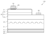
도 4는 본 발명의 일 실시예에 따른 발광 다이오드 칩(100)을 설명하기 위한 단면도이다.4 is a cross-sectional view for explaining the light emitting
도 4를 참조하면, 발광 다이오드 칩(100)은 기판(21), 발광 구조체(30), 및 DBR(43)을 포함한다. 또한, 발광 다이오드 칩(100)은 버퍼층(23), 투명 전극(31), 제1 전극 패드(33), 제2 전극 패드(35), 전류 차단층(39), 계면층(41) 및 표면층(45)을 포함할 수 있다.Referring to FIG. 4 , the light emitting
기판(21)은 투명 기판이면 특별히 한정되지 않으며, 예컨대 사파이어 또는 SiC 기판일 수 있다. 기판(21)은 질화갈륨 계열의 화합물 반도체층들을 성장시기키기에 적합한 성장기판일 수 있다. 예컨대, 기판(21)은 패터닝된 사파이어 기판(PSS)과 같이, 상부면에 소정의 패턴을 가질 수 있다. 패터닝된 사파이어 기판은 기판(21) 바닥면으로 입사되는 광이 대체로 20 내지 50도 범위 내의 입사각을 가지므로, 본원 발명의 DBR이 더욱 적합하게 그 효과를 발휘할 수 있다.The
발광 구조체(30)는 기판(21) 상부에 배치된다. 발광 구조체(30)는 제1 도전형 반도체층(25), 제2 도전형 반도체층(29) 및 상기 제1 및 제2 도전형 반도체층들(25, 29) 사이에 개재된 활성층(27)을 포함한다. 여기서, 제1 도전형과 제2 도전형은 서로 반대의 도전형으로, 제1 도전형이 n형이고, 제2 도전형이 p형일 수 있으며, 또는 그 반대일 수 있다.The
상기 제1 도전형 반도체층(25), 활성층(27) 및 제2 도전형 반도체층(29)은 질화갈륨 계열의 화합물 반도체 물질, 즉, (Al, In, Ga)N으로 형성될 수 있다. 상기 활성층(27)은 요구되는 파장의 광 예컨대 자외선 또는 청색광을 방출하도록 조성 원소 및 조성비가 결정된다. 상기 제1 도전형 반도체층(25) 및/또는 제2 도전형 반도체층(29)은, 도시한 바와 같이, 단일층으로 형성될 수 있으나, 다층 구조로 형성될 수도 있다. 또한, 활성층(27)은 단일 양자웰 또는 다중 양자웰 구조로 형성될 수 있다. 또한, 상기 기판(21)과 제1 도전형 반도체층(25) 사이에 버퍼층(23)이 개재될 수 있다.The first conductivity-
상기 반도체층들(25, 27, 29)은 MOCVD 또는 MBE 기술을 사용하여 형성될 수 있으며, 사진 및 식각 공정을 사용하여 상기 제1 도전형 반도체층(25)의 일부 영역이 노출되도록 패터닝될 수 있다.The semiconductor layers 25, 27, and 29 may be formed using MOCVD or MBE technology, and may be patterned to expose a partial region of the first conductivity
한편, 투명전극층(31)이 제2 도전형 반도체층(29) 상에, 예컨대, ITO, ZnO 또는 Ni/Au로 형성될 수 있다. 투명전극층(31)은 제2 도전형 반도체층(29)에 비해 비저항이 낮아 전류를 분산시킨다. 제1 도전형 반도체층(25) 상에 제1 전극 패드(33), 예컨대 n-전극 패드(33)가 형성되고, 투명전극층(31) 상에 제2 전극 패드(35), 예컨대 p-전극 패드(35)가 형성된다. p-전극 패드(35)는 도시한 바와 같이, 투명전극층(31)을 통해 제2 도전형 반도체층(29)에 전기적으로 접속될 수 있다.Meanwhile, the
전류 차단층(39)은 전극 패드(35)와 제2 도전형 반도체층(29) 사이에 위치한다. 상기 전류 차단층(39)은 투명 전극(39) 아래에 위치할 수 있으나, 이에 한정되는 것은 아니며, 투명 전극(39) 상에 위치할 수도 있다. 전류 차단층(39)이 투명 전극(39)과 전극 패드(35) 사이에 위치하는 경우, 전극 패드(35)는 연장부(도시하지 않음)를 통해 투명 전극(39)에 전기적으로 접속할 수 있다.The
상기 전류 차단층(39)은 활성층(27)에서 생성되어 전극 패드(35) 측으로 진행하는 광을 반사시킨다. 이러한 전류 차단층(39)은 활성층(27)에서 생성된 광에 대해 높은 반사율을 갖도록 형성될 수 있으며, 예컨대 TiO2와 SiO2와 같은 굴절률이 서로 다른 유전층들을 교대로 적층한 분포 브래그 반사기로 형성될 수 있다. 이에 따라, 상기 전극 패드(35)에 의해 광이 흡수되어 손실되는 것을 방지함으로써 발광 효율을 개선할 수 있다.The
DBR(43)은 기판(21)의 하부에 위치한다. 즉, 발광 구조체(30)와 DBR(43) 사이에 기판(21)이 배치된다. 상기 DBR(43)은 제1 굴절률(저굴절률)을 갖는 제1 재료층, 예컨대 SiO2(n: 약 1.47)와 제2 굴절률(고굴절률)을 갖는 제2 재료층, 예컨대 TiO2(n: 약 2.41)를 교대로 적층함으로써 형성된다. DBR(43)의 구체적인 적층 구조에 대해서는 도 5를 참조하여 뒤에서 상세하게 설명된다.The
한편, 기판(21)과 DBR(43) 사이에 계면층(41)이 개재될 수 있다. 계면층(41)은 제1 재료층과 동일한 재료의 층, 예컨대 SiO2층으로 형성될 수 있다. 계면층(41)은 기판(21) 바닥면에 형성되는 DBR(43)이 기판(21) 바닥면의 표면 상태에 의해 영향을 받는 것을 방지하기 위한 것으로 제1 재료층들보다 상대적으로 두껍게 형성된다. 예를 들어, 계면층(41)은 300 내지 500㎚의 두께 범위로 형성될 수 있으며, 더 구체적으로 400㎚로 형성될 수 있다.Meanwhile, an
나아가, DBR(43)의 마지막 층으로서 표면층(45)이 DBR(43)을 덮을 수 있다. 표면층(45)은 발광 다이오드 칩(100)을 패키징할 때, 발광 다이오드 칩(100)이 실장되는 실장면의 표면 상태에 의해 DBR(43)이 영향을 받는 것을 완화하기 위한 것으로, 계면층(41)과 유사하게 상대적으로 두껍게 형성된다. 예를 들어, 표면층(45)은 300 내지 500㎚의 두께 범위로 형성될 수 있으며, 더 구체적으로 400㎚로 형성될 수 있다.Furthermore, the
본 실시예에 있어서, DBR(43)은 기판(21)을 사이에 두고 발광 구조체(30)에 대향하여 배치된다. 활성층(27)에서 생성된 광은 DBR(43)에서 반사되어 발광 다이오드 칩(100)의 상방으로 방출된다.In this embodiment, the
도 4b는 본 발명의 또 다른 실시예에 따른 발광 다이오드 칩(200)을 설명하기 위한 개략적인 단면도이다.Figure 4b is a schematic cross-sectional view for explaining a light emitting
도 4b를 참조하면, 본 실시예에 있어서, DBR(53)은 DBR(47)과 대체로 유사하나, 발광 구조체(30)에 대해 기판(21)에 대향하여 배치되는 점에서 차이가 있다. DBR(53)은 도시된 바와 같이 투명 전극층(31)을 덮을 수 있으며, 제1 도전형 반도체층(25)의 노출면을 덮을 수 있다. DBR(53)은 활성층(27)에서 생성된 광을 기판(21)측으로 반사시킨다. DBR(53)의 구체적인 구조에 대해서는 도 5를 참조하여 뒤에서 상세하게 설명된다.Referring to FIG. 4B , in this embodiment, the
상기 발광 다이오드 칩(200)은 예컨대 플립칩형 발광 다이오드 칩일 수 있다. 따라서, 투명 전극층(31), n-전극 패드(33) 및 p-전극 패드(35)의 구체적인 형상 및 위치는 플립칩형 발광 다이오드 칩에 적합하게 변형될 수 있다.The light emitting
도 4a 및 도 4b를 참조하여 설명한 바와 같이, DBR(43, 53)은 기판(21) 하면에 또는 발광 구조체(30) 상부에 형성될 수 있다. 도시하지는 않았지만, DBR은 기판(21)과 발광 구조체(30)사이에 위치할 수도 있다. 이 경우, DBR은 예를 들어 반도체층들을 이용하여 형성될 수도 있을 것이다.As described with reference to FIGS. 4A and 4B , the
도 5는 본 발명의 일 실시예에 따른 DBR 구조를 설명하기 위해 제1 재료층/제2 재료층(SiO2/TiO2) 페어들의 위치별 광학 두께를 나타내는 그래프이다. 여기서, 광학 두께는 가시 영역의 중심 파장(λ:554㎚)에 대한 두께이다.FIG. 5 is a graph showing optical thicknesses of first material layer/second material layer (SiO 2 /TiO 2 ) pairs by position to describe a DBR structure according to an embodiment of the present invention. Here, the optical thickness is the thickness with respect to the central wavelength (λ: 554 nm) of the visible region.
제1 재료층과 제2 재료층의 형성 순서는 특별히 중요하지는 않으며, 구체적인 상황에 따라 변경될 수 있다. 예를 들어, 도 4a의 실시예와 같이, 제1 재료층(예, SiO2)과 동일한 재료의 계면층(41)이 형성되는 경우, DBR(43)의 첫번째 층은 제2 재료층이 될 수 있다. 이와 달리, 계면층(41)이 생략된 경우, DBR(43)의 첫번째 층은 제1 재료층이 될 수 있다. 또한, 도 4b의 실시예와 같이 계면층(41)을 필요로 하지 않는 경우, DBR(53)의 첫번째 층은 제1 재료층 또는 제2 재료층 어느 것이든 될 수 있다. 일반적으로 SiO2층의 접착력이 TiO2층보다 우수하므로, 기판(21) 또는 발광 구조체(30)에 접착되는 층을 SiO2층으로 할 수 있다.The order of formation of the first material layer and the second material layer is not particularly critical and may be changed according to specific circumstances. For example, as in the embodiment of FIG. 4A, when the
한편, DBR(43 또는 53)의 표면에 형성되는 표면층(45)은 DBR(43, 53)을 보호하는 기능을 수행하기 위해 상대적으로 두껍게 형성되며, 제1 재료층과 동일한 재료로 형성될 수 있다. 따라서, 표면층(45)을 제외한 DBR(43)의 마지막층은 일반적으로 제2 재료층이 되며, 이 층은 페어를 형성하지 못할 수도 있다.On the other hand, the
도 5는 계면층(41) 및 표면층(45) 사이에 개재된 DBR(43)로서 첫 번째 층 및 마지막 층이 제2 재료층(TiO2층)인 것을 보여주고 있다. 따라서, 제2 재료층(TiO2층)/제1 재료층(SiO2층)의 순서로 페어를 이루며, 마지막 제2 재료층은 페어를 형성하지 않는다.FIG. 5 shows that the first and last layers of the
한편, 도 5를 참조하면, DBR의 구조는 제1 영역, 제2 영역 및 제3 영역으로 뚜렷하게 구분되는 것을 확인할 수 있다. 여기서, 제1 영역이 제2 영역보다 발광 구조체(30)에 더 가깝게 배치되며, 제3 영역은 제1 영역과 제2 영역 사이에 배치된다.Meanwhile, referring to FIG. 5 , it can be seen that the structure of the DBR is clearly divided into a first region, a second region, and a third region. Here, the first region is disposed closer to the
(제1 영역)(first area)
제1 영역은 중심 파장(λ) 근처 및 중심 파장보다 장파장인 스펙트럼 영역에서의 반사율을 높이기 위해 마련된다. 따라서, 제1 영역의 제1 재료층들 및 제2 재료층들의 광학 두께는 대체로 0.25λ 근처 또는 0.25λ보다 크다.The first region is provided to increase reflectance in a spectral region near the central wavelength λ and having a longer wavelength than the central wavelength. Accordingly, the optical thickness of the first material layers and the second material layers of the first region is approximately around 0.25λ or greater than 0.25λ.
구체적으로, 제1 영역에서, 제1 재료층들(SiO2층)은 0.25λ+10%보다 큰 광학 두께를 가지는 제1군의 제1 재료층들과, 0.25λ+10%보다 작고 0.25λ-10%보다 큰 광학 두께를 가지는 제2군의 제1 재료층들로 구분된다. 이들 제1군의 제1 재료층들 및 제2 군의 제1 재료층들은 서로 교대로 배치된다. 도 5에 도시한 바와 같이, 상대적으로 두꺼운 제1군의 제1 재료층들과 상대적으로 얇은 제2군의 제1 재료층들이 서로 교대로 배치된다. 제1군의 제1 재료층이 먼저 형성될 수 있으나, 이에 한정되는 것은 아니며, 제2군의 제1 재료층이 먼저 형성될 수도 있다.Specifically, in the first region, the first material layers (SiO 2 layer) include a first group of first material layers having an optical thickness greater than 0.25λ+10% and an optical thickness less than 0.25λ+10% and 0.25λ A second group of first material layers having an optical thickness greater than -10% is distinguished. These first group first material layers and second group first material layers are alternately disposed with each other. As shown in FIG. 5, relatively thick first group first material layers and relatively thin second group first material layers are alternately disposed. The first material layer of the first group may be formed first, but is not limited thereto, and the first material layer of the second group may be formed first.
나아가, 상기 제1군의 제1 재료층들은 대체로 0.3λ+10%보다 작은 광학 두께를 갖는다. 본 실시예에 있어서, 제1군의 제1 재료층들은 5개 층들을 포함하며, 첫번째 층을 제외한 네개의 층들이 0.3λ+10%보다 작은 광학 두께를 가지는 것을 알 수 있다.Further, the first material layers of the first group generally have an optical thickness of less than 0.3λ+10%. In this embodiment, it can be seen that the first material layers of the first group include 5 layers, and the 4 layers except the first layer have an optical thickness of less than 0.3λ+10%.
한편, 상기 제1 영역 내의 제2 재료층들(예, TiO2층들)은, 0.25λ+10%보다 큰 광학 두께를 가지는 제1군의 제2 재료층들 및 0.25λ-10%보다 크고, 0.25λ+10%보다 작은 광학 두께를 가지는 제2군의 제2 재료층들을 포함한다.On the other hand, the second material layers (eg, TiO 2 layers) in the first region are the second material layers of the first group having an optical thickness greater than 0.25λ+10% and greater than 0.25λ-10%, and a second group of second material layers having an optical thickness of less than 0.25λ+10%.
제1군의 제2 재료층들 및 제2군의 제2 재료층들 또한 광학 두께가 뚜력하게 구분된다. 나아가, 이들 제1군의 제2 재료층들 및 제2군의 제2 재료층들이 모두 교대로 배치되는 것은 아니지만 대부분 서로 교대로 배치되는 것을 알 수 있다.The second material layers of the first group and the second material layers of the second group are also clearly distinguished in optical thickness. Further, it can be seen that most of the second material layers of the first group and the second material layers of the second group are not all alternately disposed, but most of them are alternately disposed.
한편, 제1군의 제2 재료층들은 대체로 제1군의 제1 재료층들보다 작은 광학 두께를 가진다. 또한, 상기 제1군의 제2 재료층들의 광학 두께의 평균값은 상기 제1군의 제1 재료층들의 광학 두께의 평균값보다 작다. 상대적으로 고굴절률을 가지는 제2 재료층들이 상대적으로 저굴절률을 가지는 제1 재료층들보다 광 흡수율이 크기 때문에, 제1군의 제2 재료층들을 상대적으로 얇게 형성함으로써 광 손실을 줄일 수 있다.On the other hand, the second material layers of the first group generally have a smaller optical thickness than the first material layers of the first group. Further, the average value of the optical thicknesses of the second material layers of the first group is smaller than the average value of the optical thicknesses of the first material layers of the first group. Since the second material layers having a relatively high refractive index have higher light absorption than the first material layers having a relatively low refractive index, light loss can be reduced by forming the second material layers of the first group relatively thin.
상기 제1군의 제2 재료층들은 0.25λ+20%(즉, 0.3λ)보다 작은 광학 두께를 가질 수 있다. 이에 반해, 제1군의 제1 재료층들은 대체로 0.25λ+20%보다 큰 광학 두께를 가진다.The second material layers of the first group may have an optical thickness of less than 0.25λ+20% (ie 0.3λ). In contrast, the first material layers of the first group generally have an optical thickness greater than 0.25λ+20%.
한편, 제2군의 제2 재료층들 또한 광 손실을 방지하기 위해 제2군의 제1 재료층들보다 작은 광학 두께를 가질 수 있으나, 제1군의 제2 재료층들에 비해 광학 두께가 상대적으로 작기 때문에 두께를 감소하더라도 광 손실을 줄이는데 큰 효과가 없다. 따라서, 제2군의 제2 재료층들과 제2군의 제1 재료층들은 대체로 유사한 광학 두께를 가질 수 있다.Meanwhile, the second material layers of the second group may also have an optical thickness smaller than that of the first material layers of the second group in order to prevent light loss, but have an optical thickness greater than that of the second material layers of the first group. Since it is relatively small, reducing the thickness does not have a significant effect on reducing light loss. Accordingly, the second group of second material layers and the second group of first material layers may have substantially similar optical thicknesses.
(제2 영역)(Second area)
제2 영역은 중심 파장(λ)보다 단파장인 스펙트럼 영역에서의 반사율을 높이기 위해 마련된다. 따라서, 제1 영역의 제1 재료층들 및 제2 재료층들의 광학 두께는 대체로 0.25λ보다 작다.The second region is provided to increase reflectance in a spectral region having a shorter wavelength than the center wavelength λ. Accordingly, the optical thickness of the first material layers and the second material layers of the first region is generally smaller than 0.25λ.
구체적으로, 제2 영역은 0.25λ-10%보다 작은 광학 두께를 가지고 연속하여 배치된 제3군의 제1 재료층들을 포함한다. 나아가, 상기 제3군의 제1 재료층들은 0.2λ-10%보다 큰 광학 두께를 가진다.Specifically, the second region includes a third group of first material layers arranged in succession with an optical thickness of less than 0.25λ-10%. Further, the first material layers of the third group have an optical thickness greater than 0.2λ-10%.
도 5에서 명확하게 알 수 있듯이, 제2 영역 내의 제1 재료층들의 광학 두께 편차는 제1 영역 내의 제1 재료층들의 광학 두께 편차보다 작다. 제1 영역 내의 제1군의 제1 재료층들 및 제2군의 제1 재료층들은 서로 뚜렷하게 다른 광학 두께를 갖기 때문에, 대체로 유사한 광학 두께를 갖는 제2 영역 내의 제1 재료층들에 비해 광학 두께 편차가 상대적으로 크게 된다.As can be clearly seen from FIG. 5 , the optical thickness deviation of the first material layers in the second region is smaller than the optical thickness deviation of the first material layers in the first region. Because the first group of first material layers and the second group of first material layers in the first region have optical thicknesses that are distinctly different from each other, they have optical thicknesses relative to first material layers in the second region that have generally similar optical thicknesses. The thickness deviation becomes relatively large.
한편, 상기 제2 영역 내의 제2 재료층들은 0.25λ-10%보다 작은 광학 두께를 가지고 연속하여 배치된 제3군의 제2 재료층들을 포함한다. 제2 영역 내에서 첫번째 제2 재료층(즉, 13번째 페어의 제2 재료층)만 0.25λ-10%보다 큰 광학 두께를 가지며 그 외의 제2 재료층들은 모두 0.25λ-10%보다 작은 광학 두께를 가진다.On the other hand, the second material layers in the second region include a third group of second material layers arranged consecutively and having an optical thickness smaller than 0.25λ-10%. Within the second region, only the first second material layer (i.e., the second material layer of the 13th pair) has an optical thickness greater than 0.25λ-10%, and all other second material layers have an optical thickness smaller than 0.25λ-10%. have a thickness
(제3 영역)(third area)
제3 영역은 제1 영역과 제2 영역 사이에 배치되며, 서로 다른 반사 대역을 가지는 DBR들을 서로 중첩할 때 발생하는 리플을 제거하기 위해 배치된다.The third region is disposed between the first region and the second region and is disposed to remove ripple generated when DBRs having different reflection bands overlap each other.
제3 영역은 대체로 적은 수의 페어들로 이루어진다. 도 5에서 알 수 있듯이, 본 실시예에 있어서, 제1 영역이 가장 많은 수의 페어들로 구성되고, 제3 영역이 가장 적은 수의 페어들로 구성된다.The third region usually consists of a small number of pairs. As can be seen from FIG. 5 , in this embodiment, the first region is composed of the largest number of pairs, and the third region is composed of the smallest number of pairs.
구체적으로, 제3 영역은 0.25λ-10%보다 작은 광학 두께를 가지는 제1 재료층, 및 0.25λ보다 큰 광학 두께를 가지는 제1 재료층을 포함한다. 나아가, 제3 영역은 0.25λ-10%보다 크고, 0.25λ보다 작은 광학 두께를 가지는 제1 재료층을 포함할 수 있다.Specifically, the third region includes a first material layer having an optical thickness less than 0.25λ-10%, and a first material layer having an optical thickness greater than 0.25λ. Further, the third region may include a first material layer having an optical thickness greater than 0.25λ-10% and less than 0.25λ.
또한, 상기 제3 영역 내의 제2 재료층들은, 0.25λ-10%보다 작은 제2 재료층, 및 0.25λ보다 크고 0.25λ+10%보다 작은 광학 두께를 가지는 제2 재료층을 포함할 수 있다. 나아가, 제3 영역 내의 제2 재료층들은, 0.25λ+10%보다 큰 광학 두께를 가지는 제2 재료층을 더 포함할 수 있다.In addition, the second material layers in the third region may include a second material layer having an optical thickness of less than 0.25λ-10% and an optical thickness of greater than 0.25λ and less than 0.25λ+10%. . Furthermore, the second material layers in the third region may further include a second material layer having an optical thickness greater than 0.25λ+10%.
상대적으로 적은 수의 페어로 구성된 제3 영역에서 제1 재료층들 및 제2 재료층들은 제1 영역 및 제2 영역 내의 재료층들에 비해 상대적으로 다양한 광학 두께를 갖도록 구성된다.In the third region composed of a relatively small number of pairs, the first material layers and the second material layers are configured to have relatively various optical thicknesses compared to the material layers in the first region and the second region.
본 실시예에 따르면, 발광 구조체(30)에 상대적으로 가깝게 배치되어 장파장 영역의 광을 반사시키는 제1 영역의 제1 및 제2 재료층들을 상대적으로 두꺼운 광학 두께를 갖는 제1군과 상대적으로 작은 광학 두께를 갖는 제2군으로 구분함으로써 입사각이 증가함에 따라 스탑 밴드 내에 발생하는 리플을 제거할 수 있다.According to the present embodiment, the first and second material layers of the first region, which are arranged relatively close to the
본 실시예에 있어서, 제1 영역이 9개의 페어로 구성되고, 제2 영역이 7.5개의 페어로 구성되고, 제3 영역이 3개의 페어로 구성되지만, 페어수는 변경될 수 있다. 다만, 제1 영역 내의 페어수가 다른 영역들보다 더 많은 것이 장파장 영역의 반사율을 보강하는데 유리할 것이다.In this embodiment, the first area is composed of 9 pairs, the second area is composed of 7.5 pairs, and the third area is composed of 3 pairs, but the number of pairs can be changed. However, it is advantageous to reinforce the reflectance of the long wavelength region when the number of pairs in the first region is greater than in other regions.
DBR을 구성하는 각 층의 광학 두께는 Macleod나 Filmstar와 같은 시뮬레이션 툴을 이용하여 조정될 수 있다. 또한, DBR의 각 재료층들은 이온 어시스트 증착 장비를 이용하여 기판(21)의 바닥면 또는 발광 구조체(30) 상부에 형성될 수 있다.The optical thickness of each layer constituting the DBR can be adjusted using a simulation tool such as Macleod or Filmstar. In addition, each material layer of the DBR may be formed on the bottom surface of the
도 6a, 6b 및 6c는 본 발명의 일 실시예에 따라 설계된 DBR의 입사각에 따른 반사율 변화를 보여주는 시뮬레이션 그래프들이다.6A, 6B, and 6C are simulation graphs showing a change in reflectance according to an incident angle of a DBR designed according to an embodiment of the present invention.
여기서, DBR의 구체적인 각 재료층들의 광학 두께는 도 5의 그래프에 나타낸 것과 같다. 또한, SiO2 계면층(41) 400㎚, SiO2 표면층(45) 400㎚를 추가하여 입사각에 따른 반사 특성 변화를 시뮬레이션하였으며, 이를 0도 입사각 그래프와 함께 나타내었다.Here, the specific optical thickness of each material layer of the DBR is as shown in the graph of FIG. 5 . In addition, 400 nm of the SiO 2 interface layer 41 and 400 nm of the SiO 2 surface layer 45 were added to simulate the change in reflection characteristics according to the incident angle, which was shown along with a 0 degree incident angle graph.
도 6a, 6b 및 6c를 참조하면, 본 실시예에 따른 DBR,은 입사각 0도인 광에 대해 약 410㎚ 내지 700㎚의 스펙트럼 영역에서 90% 이상의 반사율을 나타낸다. 따라서, 발광 다이오드 칩이 형광체와 함께 사용될 경우, 형광체에서 생성된 광이 발광 다이오드 칩으로 입사될 때 이들 광 또한 DBR을 이용하여 반사시킬 수 있다.Referring to FIGS. 6A, 6B, and 6C, the DBR according to the present embodiment shows a reflectance of 90% or more in the spectral region of about 410 nm to 700 nm with respect to light having an incident angle of 0 degrees. Therefore, when the light emitting diode chip is used together with the phosphor, when the light generated by the phosphor is incident to the light emitting diode chip, these lights can also be reflected using the DBR.
한편, 입사각이 20도, 25도 및 30도로 증가함에 따라 스탑 밴드가 단파장측으로 이동하며, 그 폭이 감소하는 것을 확인할 수 있다. 그러나 여전히 약 550㎚의 파장에서도 거의 100%의 반사율을 유지하며, 더욱이, 스탑 밴드 내에서 리플이 발생되지 않는 것을 확인할 수 있다.On the other hand, as the incident angle increases to 20 degrees, 25 degrees, and 30 degrees, it can be seen that the stop band moves to the shorter wavelength side and its width decreases. However, it can still be seen that almost 100% reflectance is maintained even at a wavelength of about 550 nm, and furthermore, no ripple occurs within the stop band.
따라서, 본 실시예에 따른 DBR은 예를 들어, 420㎚ 내지 500㎚ 사이의 청색광을 방출하는 발광 다이오드 칩에서 광을 효과적으로 반사시키기 위해 사용될 수 있다.Accordingly, the DBR according to the present embodiment may be used to effectively reflect light in a light emitting diode chip emitting blue light between 420 nm and 500 nm, for example.
한편, 본 실시예에서, DBR의 제1 영역 내에서, 광학 두께가 상대적으로 두꺼운 제1군의 제1 재료층들과 광학 두께가 상대적으로 얇은 제2군의 제1 재료층들이 교대로 배치되며, 광학 두께가 상대적으로 두꺼운 제1군의 제2 재료층들과 광학 두께가 상대적으로 얇은 제2군의 제2 재료층들 또한 대체로 교대로 배치된다. 이와 같이, 광학 두께가 서로 다른 제1 재료층들 및 제2 재료층들을 서로 교대로 배치함으로써 제1군과 제2군을 서로 분리한 경우에 비해 더 우수한 반사 특성을 나타내는 DBR을 제작할 수 있다. 이에 대해, 도 7 및 도 8을 참조하여 부가 설명한다.Meanwhile, in the present embodiment, in the first region of the DBR, the first material layers of the first group having a relatively thick optical thickness and the first material layers of the second group having a relatively thin optical thickness are alternately disposed. , the first group of second material layers having a relatively thick optical thickness and the second group of second material layers having a relatively small optical thickness are also generally alternately disposed. In this way, by alternately arranging the first material layers and the second material layers having different optical thicknesses, it is possible to fabricate a DBR having better reflection characteristics than when the first group and the second group are separated from each other. This will be further described with reference to FIGS. 7 and 8 .
도 7a는 광학 두께가 상대적으로 큰 제1 그룹의 재료층들과 상대적으로 작은 제2 그룹의 재료층들을 서로 분리하여 배치한 예를 보여주는 위치별 광학 두께의 그래프이다. 도 7b는 광학 두께가 상대적으로 큰 제1 그룹의 재료층들과 상대적으로 작은 제2 그룹의 재료층들을 서로 혼합하여 배치한 예를 보여주는 위치별 광학 두께의 그래프이다.FIG. 7A is a graph of optical thickness by position showing an example in which a first group of material layers having a relatively large optical thickness and a second group of material layers having a relatively small optical thickness are separately disposed from each other. FIG. 7B is a graph of optical thickness by position showing an example in which a first group of material layers having a relatively large optical thickness and a second group of material layers having a relatively small optical thickness are mixed and disposed.
0.3λ의 광학 두께를 갖는 제1군의 제1 재료층들 및 제2 재료층들과, 0.25λ의 광학 두께를 갖는 제2군의 제1 재료층들 및 제2 재료층들은 다양한 방법으로 배치될 수 있다. 예를 들어, 1군과 제2군이 서로 분리되도록 배치될 수도 있고(도 7a), 제1군과 제2군이 서로 교대로 배치될 수도 있다(도 7b). 여기서는 8.5페어로 DBR을 구성했다.The first group of first material layers and second material layers having an optical thickness of 0.3λ and the second group of first material layers and second material layers having an optical thickness of 0.25λ are arranged in various ways. It can be. For example,
도 8은 도 7a 및 도 7b의 DBR들의 입사각에 따른 반사율을 설명하기 위한 그래프이다. 8 is a graph for explaining the reflectance according to the incident angle of the DBRs of FIGS. 7A and 7B.
도 8을 참조하면, 도 7a에 따른 DBR의 0도 입사각에 대한 반사율(a-0도)은 뚜렷한 경계를 갖지 못하는 스탑 밴드를 보인다. 이에 반해, 도 7b에 따른 DBR의 0도 입사각에 대한 반사율(b-0도)은 뚜렷한 경계를 갖는 스탑 밴드를 보인다. 이러한 스탑 밴드의 형상은 입사각 30도에 대해서도 a-30도와 b-30도로 나타낸 바와 같이, 도 7b에 따른 DBR이 상대적으로 더 뚜렷한 경계를 보인다.Referring to FIG. 8 , the reflectance (a-0 degrees) of the DBR of FIG. 7a at an incident angle of 0 degrees shows a stop band without a clear boundary. On the other hand, the reflectance (b−0 degree) for a 0 degree incident angle of the DBR according to FIG. 7b shows a stop band with a clear boundary. As for the shape of the stop band, as shown at a-30 degrees and b-30 degrees for an incident angle of 30 degrees, the DBR according to FIG. 7B shows a relatively clear boundary.
따라서, 광학 두께가 서로 다른 재료층들을 배치할 경우, 두꺼운 재료층과 얇은 재료층을 서로 교대로 배치하는 것이 반사 특성을 강화할 수 있음을 알 수 있다.Accordingly, it can be seen that when disposing material layers having different optical thicknesses, alternately disposing thick material layers and thin material layers can enhance reflection characteristics.
한편, 종래 기술 및 본 실시예에 따라 설계된 DBR의 구조를 이용하여 FDTD 수치 분석을 이용하여 칩 레벨 및 패키지 레벨에서의 광 추출 효율을 분석하였다. DBR은 기판 하면에 위치하는 것으로 설정하였으며, 다른 구성요소는 실제 사용되는 발광 다이오드 칩의 실제 수치를 이용하였다.Meanwhile, the light extraction efficiency at the chip level and the package level was analyzed using FDTD numerical analysis using the structure of the DBR designed according to the prior art and the present embodiment. DBR was set to be located on the lower surface of the substrate, and actual values of light emitting diode chips in actual use were used for other components.
이에 따르면, 칩 레벨에서 전체 광추출 효율이 종래의 DBR을 사용한 경우(63.10%)에 비해 본 실시예에 따른 DBR을 사용한 경우(63.35%)로 약 0.25% 증가하는 것을 확인할 수 있었다. 아울러, 칩 레벨에서 기판 하부로 투과하여 방출되는 광은 종래기술에서 0.35%인 반면 본 실시예에서 0.15%로 감소하였다. 또한, 패키지 레벨에서 전체 광추출 효율은 종래의 DBR을 사용한 경우(65%)에 비해 본 실시예에 따른 DBR을 사용한 경우(65.53%)로 약 0.53% 증가하는 것을 확인할 수 있다. 이러한 광추출 효율의 증가는 모든 조건을 동일하게 하고 DBR만을 변경하여 발생된 것으로 상당히 유의미한 결과이다.According to this, it was confirmed that the overall light extraction efficiency at the chip level increased by about 0.25% in the case of using the DBR according to the present embodiment (63.35%) compared to the case of using the conventional DBR (63.10%). In addition, the light transmitted and emitted under the substrate at the chip level was 0.35% in the prior art, but decreased to 0.15% in this embodiment. In addition, it can be seen that the overall light extraction efficiency at the package level is increased by about 0.53% in the case of using the DBR according to the present embodiment (65.53%) compared to the case of using the conventional DBR (65%). This increase in light extraction efficiency was caused by keeping all conditions the same and changing only the DBR, which is a very significant result.
한편, 종래기술에 따른 DBR(비교예) 및 본 실시예에 따른 DBR(실시예)을 실제 발광 다이오드 칩에 적용하여 칩 레벨에서의 광 출력을 비교하여 도 9에 나타내었다.On the other hand, DBR (Comparative Example) according to the prior art and DBR (Example Example) according to the present embodiment are applied to an actual light emitting diode chip, and light output at a chip level is compared and shown in FIG. 9 .
도 9를 참조하면, 20mA에서 비교예는 평균 80.83mW의 광출력을 보이며, 실시예는 81.91mW의 광출력을 보였다. 따라서, DBR의 설계를 변경함으로써 발광 다이오드 칩의 광 추출효율을 개선할 수 있으며, 그에 따라 발광 다이오드 칩의 광출력을 증가시킬 수 있음을 알 수 있다.Referring to FIG. 9, at 20 mA, the comparative example showed an average light output of 80.83 mW, and the embodiment showed a light output of 81.91 mW. Therefore, it can be seen that the light extraction efficiency of the light emitting diode chip can be improved by changing the design of the DBR, and thus the light output of the light emitting diode chip can be increased.
본 실시예에서, 가시 영역의 중심 파장인 약 554㎚를 기준으로 DBR의 각 재료층의 광학 두께를 설정하였다. 발광 다이오드 칩에서 방출되는 광의 파장이 청색광인 경우, 입사각이 증가함에 따라 스탑 밴드가 단파장측으로 이동하는 것을 고려할 때, 중심 파장을 가시 영역의 중심 파장으로 설정하는 것은 의미가 있다. 더욱이, 발광 다이오드 칩이 형광체들과 함께 사용될 경우, 형광체에서 방출되는 광에 대한 반사를 고려하면, 중심 파장을 기준으로 DBR을 설계할 필요가 있다.In this embodiment, the optical thickness of each material layer of the DBR was set based on the central wavelength of about 554 nm in the visible region. When the wavelength of light emitted from the light emitting diode chip is blue light, considering that the stop band shifts to a shorter wavelength side as the incident angle increases, it is meaningful to set the center wavelength to the center wavelength of the visible region. Moreover, when a light emitting diode chip is used with phosphors, considering reflection of light emitted from the phosphors, it is necessary to design the DBR based on the center wavelength.
그러나, 본 발명은 발광 다이오드 칩이 청색광을 방출하는 것에 한정되는 것은 아니며, 또한 형광체가 함께 사용되는 것에 한정되는 것도 아니다. 따라서, 본 발명은 자외선을 방출하는 발광 다이오드 칩에도 적용될 수 있으며, 이 경우, 가시 영역의 중심 파장 대신에, 발광 다이오드 칩에서 방출되는 광의 파장(제1 파장)을 고려하여 새로운 기준 파장(제2 파장)이 선택될 수 있다.However, the present invention is not limited to a light emitting diode chip emitting blue light, nor is it limited to using a phosphor together. Therefore, the present invention can also be applied to a light emitting diode chip that emits ultraviolet rays. In this case, instead of the center wavelength of the visible region, a new reference wavelength (second wavelength) is considered by considering the wavelength (first wavelength) of light emitted from the light emitting diode chip. wavelength) can be selected.
제2 파장은 제1 파장에 비해 75 내지 125㎚ 범위 내의 파장만큼 더 장파장일 수 있다. 입사각이 증가함에 따라 스탑 밴드가 단파장측으로 이동하더라도, 제2 파장을 위와 같이 설정함으로써, 발광 다이오드 칩에서 방출되는 광에 대해 높은 반사율을 유지할 수 있다. 제2 파장이 제1 파장에 비해 75㎚ 미만의 장파장인 경우, 제1 파장과 제2 파장이 너무 가까워서 입사각이 증가함에 따라 제1 파장의 광에 대한 반사율이 감소할 수 있다. 또한, 제2 파장이 제1 파장에 비해 125㎚ 이상 긴 장파장인 경우, 0도 입사각에서 제1 파장에 대한 반사율이 높은 DBR을 제작하는 것이 어려울 수 있다. 구체적으로, 상기 제2 파장은 제1 파장에 비해 약 100㎚ 긴 파장일 수 있다.The second wavelength may have a longer wavelength than the first wavelength by a wavelength within a range of 75 to 125 nm. Even if the stop band shifts to a shorter wavelength side as the incident angle increases, by setting the second wavelength as described above, a high reflectance of light emitted from the light emitting diode chip can be maintained. When the second wavelength has a longer wavelength of less than 75 nm compared to the first wavelength, the reflectance of the light of the first wavelength may decrease as the incident angle increases because the first wavelength and the second wavelength are too close. In addition, when the second wavelength is longer than the first wavelength by 125 nm or more, it may be difficult to manufacture a DBR having a high reflectance for the first wavelength at a 0 degree incident angle. Specifically, the second wavelength may be about 100 nm longer than the first wavelength.
중심 파장(554㎚) 대신에 상기 제2 파장을 기준으로 설정하는 이외에, 제1 재료층들 및 제2 재료층들의 광학 두께는 앞서의 실시예에서 설명한 바와 같이 설정될 수 있을 것이다.In addition to setting the second wavelength as a reference instead of the central wavelength (554 nm), the optical thickness of the first material layers and the second material layers may be set as described in the previous embodiment.
한편, 제1 재료층 및 제2 재료층으로 SiO2와 TiO2를 예로 들었지만, 본 발명은 이들 재료층에 한정되는 것은 아니며, 다른 절연층들 또는 반도체층들이 사용될 수 있다.Meanwhile, although SiO 2 and TiO 2 are exemplified as the first material layer and the second material layer, the present invention is not limited to these material layers, and other insulating layers or semiconductor layers may be used.
도 10은 본 발명의 일 실시예에 따른 발광 소자(발광 다이오드 칩)을 적용한 조명 장치를 설명하기 위한 분해 사시도이다.10 is an exploded perspective view for explaining a lighting device to which a light emitting device (light emitting diode chip) according to an embodiment of the present invention is applied.
도 10을 참조하면, 본 실시예에 따른 조명 장치는, 확산 커버(1010), 발광 소자 모듈(1020) 및 바디부(1030)를 포함한다. 바디부(1030)는 발광 소자 모듈(1020)을 수용할 수 있고, 확산 커버(1010)는 발광 소자 모듈(1020)의 상부를 커버할 수 있도록 바디부(1030) 상에 배치될 수 있다.Referring to FIG. 10 , the lighting device according to the present embodiment includes a
바디부(1030)는 발광 소자 모듈(1020)을 수용 및 지지하여, 발광 소자 모듈(1020)에 전기적 전원을 공급할 수 있는 형태이면 제한되지 않는다. 예를 들어, 도시된 바와 같이, 바디부(1030)는 바디 케이스(1031), 전원 공급 장치(1033), 전원 케이스(1035), 및 전원 접속부(1037)를 포함할 수 있다. The
전원 공급 장치(1033)는 전원 케이스(1035) 내에 수용되어 발광 소자 모듈(1020)과 전기적으로 연결되며, 적어도 하나의 IC칩을 포함할 수 있다. 상기 IC칩은 발광 소자 모듈(1020)로 공급되는 전원의 특성을 조절, 변환 또는 제어할 수 있다. 전원 케이스(1035)는 전원 공급 장치(1033)를 수용하여 지지할 수 있고, 전원 공급 장치(1033)가 그 내부에 고정된 전원 케이스(1035)는 바디 케이스(1031)의 내부에 위치할 수 있다. 전원 접속부(115)는 전원 케이스(1035)의 하단에 배치되어, 전원 케이스(1035)와 결속될 수 있다. 이에 따라, 전원 접속부(1037)는 전원 케이스(1035) 내부의 전원 공급 장치(1033)와 전기적으로 연결되어, 외부 전원이 전원 공급 장치(1033)에 공급될 수 있는 통로 역할을 할 수 있다.The
발광 소자 모듈(1020)은 기판(1023) 및 기판(1023) 상에 배치된 발광 소자(1021)를 포함한다. 발광 소자 모듈(1020)은 바디 케이스(1031) 상부에 마련되어 전원 공급 장치(1033)에 전기적으로 연결될 수 있다.The light emitting
기판(1023)은 발광 소자(1021)를 지지할 수 있는 기판이면 제한되지 않으며, 예를 들어, 배선을 포함하는 인쇄회로기판일 수 있다. 기판(1023)은 바디 케이스(1031)에 안정적으로 고정될 수 있도록, 바디 케이스(1031) 상부의 고정부에 대응하는 형태를 가질 수 있다. 발광 소자(1021)는 상술한 본 발명의 실시예들에 따른 발광 소자들 중 적어도 하나를 포함할 수 있다. The
확산 커버(1010)는 발광 소자(1021) 상에 배치되되, 바디 케이스(1031)에 고정되어 발광 소자(1021)를 커버할 수 있다. 확산 커버(1010)는 투광성 재질을 가질 수 있으며, 확산 커버(1010)의 형태 및 광 투과성을 조절하여 조명 장치의 지향 특성을 조절할 수 있다. 따라서 확산 커버(1010)는 조명 장치의 이용 목적 및 적용 태양에 따라 다양한 형태로 변형될 수 있다.The
도 11은 본 발명의 또 다른 실시예에 따른 발광 소자를 적용한 디스플레이 장치를 설명하기 위한 단면도이다.11 is a cross-sectional view for explaining a display device to which a light emitting device according to another embodiment of the present invention is applied.
본 실시예의 디스플레이 장치는 표시패널(2110), 표시패널(2110)에 광을 제공하는 백라이트 유닛 및, 상기 표시패널(2110)의 하부 가장자리를 지지하는 패널 가이드를 포함한다.The display device of this embodiment includes a
표시패널(2110)은 특별히 한정되지 않고, 예컨대, 액정층을 포함하는 액정표시패널일 수 있다. 표시패널(2110)의 가장자리에는 상기 게이트 라인으로 구동신호를 공급하는 게이트 구동 PCB가 더 위치할 수 있다. 여기서, 게이트 구동 PCB는 별도의 PCB에 구성되지 않고, 박막 트랜지스터 기판상에 형성될 수도 있다.The
백라이트 유닛은 적어도 하나의 기판 및 복수의 발광 소자(2160)를 포함하는 광원 모듈을 포함한다. 나아가, 백라이트 유닛은 바텀커버(2180), 반사 시트(2170), 확산 플레이트(2131) 및 광학 시트들(2130)을 더 포함할 수 있다.The backlight unit includes a light source module including at least one substrate and a plurality of
바텀커버(2180)는 상부로 개구되어, 기판, 발광 소자(2160), 반사 시트(2170), 확산 플레이트(2131) 및 광학 시트들(2130)을 수납할 수 있다. 또한, 바텀커버(2180)는 패널 가이드와 결합될 수 있다. 기판은 반사 시트(2170)의 하부에 위치하여, 반사 시트(2170)에 둘러싸인 형태로 배치될 수 있다. 다만, 이에 한정되지 않고, 반사 물질이 표면에 코팅된 경우에는 반사 시트(2170) 상에 위치할 수도 있다. 또한, 기판은 복수로 형성되어, 복수의 기판들이 나란히 배치된 형태로 배치될 수 있으나, 이에 한정되지 않고, 단일의 기판으로 형성될 수도 있다.The
발광 소자(2160)는 상술한 본 발명의 실시예들에 따른 발광 소자들 중 적어도 하나를 포함할 수 있다. 발광 소자(2160)들은 기판 상에 일정한 패턴으로 규칙적으로 배열될 수 있다. 또한, 각각의 발광 소자(2160) 상에는 렌즈(2210)가 배치되어, 복수의 발광 소자(2160)들로부터 방출되는 광을 균일성을 향상시킬 수 있다.The
확산 플레이트(2131) 및 광학 시트들(2130)은 발광 소자(2160) 상에 위치한다. 발광 소자(2160)로부터 방출된 광은 확산 플레이트(2131) 및 광학 시트들(2130)을 거쳐 면 광원 형태로 표시패널(2110)로 공급될 수 있다. A diffusion plate 2131 and
이와 같이, 본 발명의 실시예들에 따른 발광 소자는 본 실시예와 같은 직하형 디스플레이 장치에 적용될 수 있다.In this way, the light emitting device according to the embodiments of the present invention can be applied to a direct type display device like the present embodiment.
도 12는 본 발명의 또 다른 실시예에 따른 발광 소자(발광 다이오드 칩)를 적용한 디스플레이 장치를 설명하기 위한 단면도이다. 12 is a cross-sectional view illustrating a display device to which a light emitting element (light emitting diode chip) according to another embodiment of the present invention is applied.
본 실시예에 따른 백라이트 유닛이 구비된 디스플레이 장치는 영상이 디스플레이되는 표시패널(3210), 표시패널(3210)의 배면에 배치되어 광을 조사하는 백라이트 유닛을 포함한다. 나아가, 상기 디스플레이 장치는, 표시패널(3210)을 지지하고 백라이트 유닛이 수납되는 프레임(240) 및 상기 표시패널(3210)을 감싸는 커버(3240, 3280)를 포함한다.A display device with a backlight unit according to the present embodiment includes a
표시패널(3210)은 특별히 한정되지 않고, 예컨대, 액정층을 포함하는 액정표시패널일 수 있다. 표시패널(3210)의 가장자리에는 상기 게이트 라인으로 구동신호를 공급하는 게이트 구동 PCB가 더 위치할 수 있다. 여기서, 게이트 구동 PCB는 별도의 PCB에 구성되지 않고, 박막 트랜지스터 기판상에 형성될 수도 있다. 표시패널(3210)은 그 상하부에 위치하는 커버(3240, 3280)에 의해 고정되며, 하부에 위치하는 커버(3280)는 백라이트 유닛과 결속될 수 있다.The
표시패널(3210)에 광을 제공하는 백라이트 유닛은 상면의 일부가 개구된 하부 커버(3270), 하부 커버(3270)의 내부 일 측에 배치된 광원 모듈 및 상기 광원 모듈과 나란하게 위치되어 점광을 면광으로 변환하는 도광판(3250)을 포함한다. 또한, 본 실시예의 백라이트 유닛은 도광판(3250) 상에 위치되어 광을 확산 및 집광시키는 광학 시트들(3230), 도광판(3250)의 하부에 배치되어 도광판(3250)의 하부방향으로 진행하는 광을 표시패널(3210) 방향으로 반사시키는 반사시트(3260)를 더 포함할 수 있다.The backlight unit providing light to the
광원 모듈은 기판(3220) 및 상기 기판(3220)의 일면에 일정 간격으로 이격되어 배치된 복수의 발광 소자(3110)를 포함한다. 기판(3220)은 발광 소자(3110)를 지지하고 발광 소자(3110)에 전기적으로 연결된 것이면 제한되지 않으며, 예컨대, 인쇄회로기판일 수 있다. 발광 소자(3110)는 상술한 본 발명의 실시예들에 따른 발광 소자를 적어도 하나 포함할 수 있다. 광원 모듈로부터 방출된 광은 도광판(3250)으로 입사되어 광학 시트들(3230)을 통해 표시패널(3210)로 공급된다. 도광판(3250) 및 광학 시트들(3230)을 통해, 발광 소자(3110)들로부터 방출된 점 광원이 면 광원으로 변형될 수 있다.The light source module includes a
이와 같이, 본 발명의 실시예들에 따른 발광 소자는 본 실시예와 같은 에지형 디스플레이 장치에 적용될 수 있다.In this way, the light emitting device according to the embodiments of the present invention can be applied to an edge type display device like the present embodiment.
도 13은 본 발명의 또 다른 실시예에 따른 발광 소자(발광 다이오드 칩)를 헤드 램프에 적용한 예를 설명하기 위한 단면도이다.13 is a cross-sectional view for explaining an example in which a light emitting device (light emitting diode chip) according to another embodiment of the present invention is applied to a headlamp.
도 13을 참조하면, 상기 헤드 램프는, 램프 바디(4070), 기판(4020), 발광 소자(4010) 및 커버 렌즈(4050)를 포함한다. 나아가, 상기 헤드 램프는, 방열부(4030), 지지랙(4060) 및 연결 부재(4040)를 더 포함할 수 있다.Referring to FIG. 13 , the headlamp includes a
기판(4020)은 지지랙(4060)에 의해 고정되어 램프 바디(4070) 상에 이격 배치된다. 기판(4020)은 발광 소자(4010)를 지지할 수 있는 기판이면 제한되지 않으며, 예컨대, 인쇄회로기판과 같은 도전 패턴을 갖는 기판일 수 있다. 발광 소자(4010)는 기판(4020) 상에 위치하며, 기판(4020)에 의해 지지 및 고정될 수 있다. 또한, 기판(4020)의 도전 패턴을 통해 발광 소자(4010)는 외부의 전원과 전기적으로 연결될 수 있다. 또한, 발광 소자(4010)는 상술한 본 발명의 실시예들에 따른 발광 소자를 적어도 하나 포함할 수 있다. The
커버 렌즈(4050)는 발광 소자(4010)로부터 방출되는 광이 이동하는 경로 상에 위치한다. 예컨대, 도시된 바와 같이, 커버 렌즈(4050)는 연결 부재(4040)에 의해 발광 소자(4010)로부터 이격되어 배치될 수 있고, 발광 소자(4010)로부터 방출된 광을 제공하고자하는 방향에 배치될 수 있다. 커버 렌즈(4050)에 의해 헤드 램프로부터 외부로 방출되는 광의 지향각 및/또는 색상이 조절될 수 있다. 한편, 연결 부재(4040)는 커버 렌즈(4050)를 기판(4020)과 고정시킴과 아울러, 발광 소자(4010)를 둘러싸도록 배치되어 발광 경로(4045)를 제공하는 광 가이드 역할을 할 수도 있다. 이때, 연결 부재(4040)는 광 반사성 물질로 형성되거나, 광 반사성 물질로 코팅될 수 있다. 한편, 방열부(4030)는 방열핀(4031) 및/또는 방열팬(4033)을 포함할 수 있고, 발광 소자(4010) 구동 시 발생하는 열을 외부로 방출시킨다.The
이와 같이, 본 발명의 실시예들에 따른 발광 소자는 본 실시예와 같은 헤드 램프, 특히, 차량용 헤드 램프에 적용될 수 있다.In this way, the light emitting device according to the embodiments of the present invention can be applied to a headlamp like the present embodiment, in particular, a vehicle headlamp.
이상에서, 본 발명의 다양한 실시예들에 대하여 설명하였지만, 상술한 다양한 실시예들 및 특징들에 본 발명이 한정되는 것은 아니고, 본 발명의 특허청구범위에 의한 기술적 사상을 벗어나지 않는 범위 내에서 다양한 변형과 변경이 가능하다.In the above, various embodiments of the present invention have been described, but the present invention is not limited to the various embodiments and features described above, and various Transformation and change are possible.
21: 기판
30: 발광 구조체
41: 계면층
43, 53: 분포 브래그 반사기(DBR)
100, 200: 발광 다이오드 칩21: substrate
30: light emitting structure
41: interface layer
43, 53: Distributed Bragg Reflector (DBR)
100, 200: light emitting diode chip
Claims (20)
상기 발광 구조체에서 방출된 광을 반사하도록 상기 발광 구조체의 일측에 배치된 분포 브래그 반사기(DBR)를 포함하고,
상기 DBR은 서로 교대로 적층된 저굴절률을 갖는 제1 재료층들 및 고굴절률을 갖는 제2 재료층들을 포함하며, 가시 영역의 중심 파장(λ:554㎚)에 대해,
0.25λ+10%보다 큰 광학 두께를 가지는 제1군의 제1 재료층들과, 0.25λ+10%보다 작고 0.25λ-10%보다 큰 광학 두께를 가지는 제2군의 제1 재료층들이 서로 교대로 배치된 제1 영역;
0.25λ-10%보다 작은 광학 두께를 가지고 연속하여 배치된 제3군의 제1 재료층들을 포함하는 제2 영역; 및
상기 제1 영역과 제2 영역 사이에 위치하고, 0.25λ-10%보다 작은 광학 두께를 가지는 제1 재료층, 및 0.25λ보다 큰 광학 두께를 가지는 제1 재료층을 포함하는 제3 영역을 포함하고,
상기 제1 영역이 상기 제2 영역보다 상기 발광 구조체에 더 가깝게 위치하는 발광 다이오드 칩.A light emitting structure including an active layer; and
A distributed Bragg reflector (DBR) disposed on one side of the light emitting structure to reflect light emitted from the light emitting structure;
The DBR includes first material layers having a low refractive index and second material layers having a high refractive index that are alternately stacked with each other, and for a central wavelength (λ: 554 nm) of the visible region,
The first material layers of the first group having an optical thickness greater than 0.25λ + 10% and the first material layers of the second group having an optical thickness less than 0.25λ + 10% and greater than 0.25λ-10% mutually alternating first regions;
a second region comprising a third group of first material layers disposed consecutively and having an optical thickness of less than 0.25λ-10%; and
a third region located between the first region and the second region and comprising a first material layer having an optical thickness of less than 0.25λ-10%, and a first material layer having an optical thickness greater than 0.25λ; ,
The light emitting diode chip wherein the first region is located closer to the light emitting structure than the second region.
상기 제1군의 제1 재료층들은 0.3λ+10%보다 작은 광학 두께를 가지는 제1 재료층들을 포함하고,
상기 제3군의 제1 재료층들은 0.2λ-10%보다 큰 광학 두께를 가지는 발광 다이오드 칩.The method of claim 1,
the first group of first material layers comprises first material layers having an optical thickness of less than 0.3λ+10%;
The first material layers of the third group have an optical thickness greater than 0.2λ-10%.
상기 제1 영역 내의 제1 재료층들의 광학 두께 편차가 상기 제2 영역 내의 제1 재료층들의 광학 두께 편차보다 큰 발광 다이오드 칩.The method of claim 2,
The optical thickness deviation of the first material layers in the first region is greater than the optical thickness deviation of the first material layers in the second region.
상기 제1 영역 내의 제2 재료층들은, 0.25λ+10%보다 큰 광학 두께를 가지는 제1군의 제2 재료층들 및 0.25λ-10%보다 크고, 0.25λ+10%보다 작은 광학 두께를 가지는 제2군의 제2 재료층들을 포함하고,
상기 제2 영역 내의 제2 재료층들은 0.25λ-10%보다 작은 광학 두께를 가지고 연속하여 배치된 제3군의 제2 재료층들을 포함하고,
상기 제3 영역 내의 제2 재료층들은, 0.25λ-10%보다 작은 광학 두께를 가지는 제2 재료층, 및 0.25λ보다 크고 0.25λ+10%보다 작은 광학 두께를 가지는 제2 재료층을 포함하는 발광 다이오드 칩.The method according to any one of claims 1 to 3,
The second material layers in the first region have a first group of second material layers having an optical thickness greater than 0.25λ+10% and an optical thickness greater than 0.25λ-10% and less than 0.25λ+10%. The branch comprises a second group of second material layers;
the second material layers in the second region include a third group of second material layers arranged in succession with an optical thickness of less than 0.25λ-10%;
wherein the second material layers in the third region include a second material layer having an optical thickness of less than 0.25λ-10%, and a second material layer having an optical thickness of greater than 0.25λ and less than 0.25λ+10%. light emitting diode chip.
상기 제1군의 제2 재료층들은 0.25λ+20%보다 작은 광학 두께를 가지는 발광 다이오드 칩.The method of claim 4,
The light emitting diode chip of claim 1 , wherein the second material layers of the first group have an optical thickness of less than 0.25λ+20%.
상기 제1군의 제2 재료층들의 광학 두께의 평균값은 상기 제1군의 제1 재료층들의 광학 두께의 평균값보다 작은 발광 다이오드 칩.The method of claim 5,
The average value of the optical thicknesses of the second material layers of the first group is smaller than the average value of the optical thicknesses of the first material layers of the first group.
상기 제1 영역 내의 제2 재료층들의 광학 두께 편차가 상기 제2 영역 내의 제2 재료층들의 광학 두께 편차보다 큰 발광 다이오드 칩.The method of claim 4,
The optical thickness deviation of the second material layers in the first region is greater than the optical thickness deviation of the second material layers in the second region.
상기 제3 영역 내의 제2 재료층들은, 0.25λ+10%보다 큰 광학 두께를 가지는 제2 재료층을 더 포함하는 발광 다이오드 칩.The method of claim 4,
The second material layers in the third region further include a second material layer having an optical thickness greater than 0.25λ+10%.
상기 DBR은 상기 제3 영역 내에 위치하고, 0.25λ-10%보다 크고 0.25λ보다 작은 광학 두께를 가지는 제1 재료층을 더 포함하는 발광 다이오드 칩.The method of claim 8,
wherein the DBR further comprises a first material layer positioned within the third region and having an optical thickness greater than 0.25λ-10% and less than 0.25λ.
상기 발광 구조체와 상기 DBR 사이에 배치된 기판을 더 포함하는 발광 다이오드 칩.The method of claim 1,
A light emitting diode chip further comprising a substrate disposed between the light emitting structure and the DBR.
상기 기판은 패터닝된 사파이어 기판(PSS)인 발광 다이오드 칩.The method of claim 10,
The substrate is a patterned sapphire substrate (PSS) light emitting diode chip.
상기 기판과 상기 DBR 사이에 상기 DBR 내의 제1 재료층들과 동일한 재료로 형성되고, 상기 제1 재료층들보다 상대적으로 더 두꺼운 계면층을 더 포함하는 발광 다이오드 칩.The method of claim 10,
The light emitting diode chip further comprises an interface layer formed of the same material as the first material layers in the DBR and relatively thicker than the first material layers in the DBR between the substrate and the DBR.
상기 계면층에 대향하여 상기 DBR의 마지막 층 상에 위치하되, 상기 DBR 내의 제1 재료층들과 동일한 재료로 형성되고, 상기 제1 재료층들보다 상대적으로 더 두꺼운 표면층을 더 포함하는 발광 다이오드 칩.The method of claim 12,
A light emitting diode chip further comprising a surface layer positioned on a last layer of the DBR opposite to the interface layer, formed of the same material as first material layers in the DBR, and relatively thicker than the first material layers. .
상기 발광 구조체를 사이에 두고 상기 DBR에 대향하여 배치된 기판을 더 포함하는 발광 다이오드 칩.The method of claim 1,
The light emitting diode chip further comprises a substrate disposed to face the DBR with the light emitting structure interposed therebetween.
상기 활성층은 청색광을 생성하는 발광 다이오드 칩.The method of claim 1,
The active layer is a light emitting diode chip that generates blue light.
상기 제1 재료층들은 SiO2층이고,
상기 제2 재료층들은 TiO2층인 발광 다이오드 칩.The method of claim 1,
The first material layers are SiO 2 layers,
The second material layers are TiO 2 layers.
상기 발광 구조체에서 방출된 광을 반사하도록 상기 발광 구조체의 일측에 배치된 분포 브래그 반사기(DBR)를 포함하고,
상기 DBR은 서로 교대로 적층된 저굴절률을 갖는 제1 재료층들 및 고굴절률을 갖는 제2 재료층들을 포함하며, 상기 제1 파장보다 75 내지 125㎚ 범위 내의 길이만큼 긴 제2 파장(λ)에 대해,
0.25λ+10%보다 큰 광학 두께를 가지는 제1군의 제1 재료층들과, 0.25λ+10%보다 작고 0.25λ-10%보다 큰 광학 두께를 가지는 제2군의 제1 재료층들이 서로 교대로 배치된 제1 영역;
0.25λ-10%보다 작은 광학 두께를 가지고 연속하여 배치된 제3군의 제1 재료층들을 포함하는 제2 영역; 및
상기 제1 영역과 제2 영역 사이에 위치하고, 0.25λ-10%보다 작은 광학 두께를 가지는 제1 재료층, 및 0.25λ보다 큰 광학 두께를 가지는 제1 재료층을 포함하는 제3 영역을 포함하고,
상기 제1 영역이 상기 제2 영역보다 상기 발광 구조체에 더 가깝게 위치하는 발광 다이오드 칩.a light emitting structure including an active layer emitting light of a first wavelength; and
A distributed Bragg reflector (DBR) disposed on one side of the light emitting structure to reflect light emitted from the light emitting structure;
The DBR includes first material layers having a low refractive index and second material layers having a high refractive index that are alternately stacked with each other, and has a second wavelength (λ) longer than the first wavelength by a length within a range of 75 to 125 nm. About,
The first material layers of the first group having an optical thickness greater than 0.25λ + 10% and the first material layers of the second group having an optical thickness less than 0.25λ + 10% and greater than 0.25λ-10% mutually alternating first regions;
a second region comprising a third group of first material layers disposed consecutively and having an optical thickness of less than 0.25λ-10%; and
a third region located between the first region and the second region and comprising a first material layer having an optical thickness of less than 0.25λ-10%, and a first material layer having an optical thickness greater than 0.25λ; ,
The light emitting diode chip wherein the first region is located closer to the light emitting structure than the second region.
상기 제1군의 제1 재료층들은 0.3λ+10%보다 작은 광학 두께를 가지는 제1 재료층들을 포함하고,
상기 제3군의 제1 재료층들은 0.2λ-10%보다 큰 광학 두께를 가지는 발광 다이오드 칩.The method of claim 17
the first group of first material layers comprises first material layers having an optical thickness of less than 0.3λ+10%;
The first material layers of the third group have an optical thickness greater than 0.2λ-10%.
상기 제1 영역 내의 제1 재료층들의 광학 두께 편차가 상기 제2 영역 내의 제1 재료층들의 광학 두께 편차보다 큰 발광 다이오드 칩.The method of claim 17
The optical thickness deviation of the first material layers in the first region is greater than the optical thickness deviation of the first material layers in the second region.
상기 제1 영역 내의 제2 재료층들은, 0.25λ+10%보다 큰 광학 두께를 가지는 제1군의 제2 재료층들 및 0.25λ-10%보다 크고, 0.25λ+10%보다 작은 광학 두께를 가지는 제2군의 제2 재료층들을 포함하고,
상기 제2 영역 내의 제2 재료층들은 0.25λ-10%보다 작은 광학 두께를 가지고 연속하여 배치된 제3군의 제2 재료층들을 포함하고,
상기 제3 영역 내의 제2 재료층들은, 0.25λ-10%보다 작은 광학 두께를 가지는 제2 재료층, 및 0.25λ보다 크고 0.25λ+10%보다 작은 광학 두께를 가지는 제2 재료층을 포함하는 발광 다이오드 칩.The method according to any one of claims 15 to 17,
The second material layers in the first region have a first group of second material layers having an optical thickness greater than 0.25λ+10% and an optical thickness greater than 0.25λ-10% and less than 0.25λ+10%. The branch comprises a second group of second material layers;
the second material layers in the second region include a third group of second material layers arranged in succession with an optical thickness of less than 0.25λ-10%;
wherein the second material layers in the third region include a second material layer having an optical thickness of less than 0.25λ-10%, and a second material layer having an optical thickness of greater than 0.25λ and less than 0.25λ+10%. light emitting diode chip.
Priority Applications (10)
| Application Number | Priority Date | Filing Date | Title |
|---|---|---|---|
| KR1020150148036A KR102471102B1 (en) | 2015-10-23 | 2015-10-23 | Light emitting diode chip having distributed bragg reflector |
| EP16857630.4A EP3353821B1 (en) | 2015-10-23 | 2016-06-17 | Light emitting diode chip having distributed bragg reflector |
| US15/767,284 US10804437B2 (en) | 2015-10-23 | 2016-06-17 | Light emitting diode chip having distributed Bragg reflector |
| PCT/KR2016/006428 WO2017069372A1 (en) | 2015-10-23 | 2016-06-17 | Light emitting diode chip having distributed bragg reflector |
| TW106139078A TWI665810B (en) | 2015-10-23 | 2016-07-12 | Light emitting diode chip having distributed bragg reflector |
| TW105121835A TWI613839B (en) | 2015-10-23 | 2016-07-12 | Light emitting diode chip having distributed bragg reflector |
| CN201610670509.6A CN106611811B (en) | 2015-10-23 | 2016-08-15 | Light-emitting diode chip for backlight unit with distributed Bragg reflector |
| JP2016162217A JP6275788B2 (en) | 2015-10-23 | 2016-08-22 | Light emitting diode chip with distributed Bragg reflector |
| JP2018002039A JP6831801B2 (en) | 2015-10-23 | 2018-01-10 | Light emitting diode chip with distributed Bragg reflector |
| US17/016,371 US20200411725A1 (en) | 2015-10-23 | 2020-09-10 | Light emitting diode chip having distributed bragg reflector |
Applications Claiming Priority (1)
| Application Number | Priority Date | Filing Date | Title |
|---|---|---|---|
| KR1020150148036A KR102471102B1 (en) | 2015-10-23 | 2015-10-23 | Light emitting diode chip having distributed bragg reflector |
Publications (2)
| Publication Number | Publication Date |
|---|---|
| KR20170047664A KR20170047664A (en) | 2017-05-08 |
| KR102471102B1 true KR102471102B1 (en) | 2022-11-25 |
Family
ID=58557709
Family Applications (1)
| Application Number | Title | Priority Date | Filing Date |
|---|---|---|---|
| KR1020150148036A KR102471102B1 (en) | 2015-10-23 | 2015-10-23 | Light emitting diode chip having distributed bragg reflector |
Country Status (7)
| Country | Link |
|---|---|
| US (2) | US10804437B2 (en) |
| EP (1) | EP3353821B1 (en) |
| JP (2) | JP6275788B2 (en) |
| KR (1) | KR102471102B1 (en) |
| CN (1) | CN106611811B (en) |
| TW (2) | TWI665810B (en) |
| WO (1) | WO2017069372A1 (en) |
Families Citing this family (25)
| Publication number | Priority date | Publication date | Assignee | Title |
|---|---|---|---|---|
| CN116884966A (en) | 2017-07-21 | 2023-10-13 | 日亚化学工业株式会社 | Backlight device and light source |
| JP7082273B2 (en) | 2017-07-21 | 2022-06-08 | 日亜化学工業株式会社 | Light emitting device, integrated light emitting device and light emitting module |
| KR20190022326A (en) * | 2017-08-24 | 2019-03-06 | 서울바이오시스 주식회사 | Light emitting diode having distributed bragg reflector |
| CN108134005B (en) * | 2017-12-13 | 2023-12-22 | 华灿光电(浙江)有限公司 | Light-emitting diode chip and preparation method thereof |
| CN108172673B (en) * | 2018-01-31 | 2023-10-13 | 江苏新广联科技股份有限公司 | Manufacturing method and structure of distributed Bragg reflector pattern for LED flip chip |
| US10340480B1 (en) | 2018-03-01 | 2019-07-02 | Avalon Holographics Inc. | OLED microcavity design and optimization method |
| US11799058B2 (en) * | 2018-03-15 | 2023-10-24 | Osram Oled Gmbh | Optoelectronic semiconductor chip |
| DE102018107673A1 (en) | 2018-03-15 | 2019-09-19 | Osram Opto Semiconductors Gmbh | Optoelectronic semiconductor chip and production method for an optoelectronic semiconductor chip |
| CN108447955B (en) | 2018-03-16 | 2019-07-23 | 厦门市三安光电科技有限公司 | LED chip construction and preparation method thereof |
| KR102496316B1 (en) * | 2018-05-30 | 2023-02-07 | 서울바이오시스 주식회사 | Light emitting diode chip having distributed bragg reflector |
| US11469349B2 (en) * | 2018-07-17 | 2022-10-11 | Xiamen Changelight Co., Ltd. | Semiconductor chip of light emitting diode and manufacturing method thereof |
| KR102624112B1 (en) * | 2018-10-23 | 2024-01-12 | 서울바이오시스 주식회사 | Flip chip type light emitting diode chip |
| MX2021009299A (en) * | 2019-01-31 | 2022-01-24 | Seoul Viosys Co Ltd | Light-emitting diode. |
| KR102610626B1 (en) * | 2019-01-31 | 2023-12-07 | 서울바이오시스 주식회사 | Light emitting diode having solder bump |
| KR102632226B1 (en) * | 2019-01-31 | 2024-02-02 | 서울바이오시스 주식회사 | Light emitting diode having distributed bragg reflector |
| JP6811293B1 (en) | 2019-08-21 | 2021-01-13 | 日機装株式会社 | Semiconductor light emitting element and manufacturing method of semiconductor light emitting element |
| DE102019122593A1 (en) * | 2019-08-22 | 2021-02-25 | OSRAM Opto Semiconductors Gesellschaft mit beschränkter Haftung | Optoelectronic semiconductor chip |
| JP2021114594A (en) * | 2019-08-27 | 2021-08-05 | 株式会社東芝 | Optical semiconductor element |
| TWI785383B (en) * | 2020-09-16 | 2022-12-01 | 晶元光電股份有限公司 | Semiconductor light-emitting device having distributed bragg reflector |
| CN116632132A (en) * | 2020-11-19 | 2023-08-22 | 厦门三安光电有限公司 | DBR structure, LED chip, semiconductor light-emitting device, manufacturing method and display panel |
| US20220173080A1 (en) * | 2020-11-30 | 2022-06-02 | Seoul Viosys Co., Ltd. | Unit pixel and displaying apparatus including the unit pixel |
| CN112909139A (en) * | 2021-02-01 | 2021-06-04 | 扬州乾照光电有限公司 | LED chip based on DBR structure and preparation method thereof |
| CN113193090B (en) * | 2021-04-27 | 2023-06-06 | 錼创显示科技股份有限公司 | Micro light-emitting diode structure and micro light-emitting diode display panel using same |
| TWI792283B (en) | 2021-04-27 | 2023-02-11 | 錼創顯示科技股份有限公司 | Micro light-emitting diode structure and micro light-emitting diode display panel using the same |
| CN113471342B (en) * | 2021-06-30 | 2022-12-02 | 厦门士兰明镓化合物半导体有限公司 | LED epitaxial structure and LED chip |
Citations (2)
| Publication number | Priority date | Publication date | Assignee | Title |
|---|---|---|---|---|
| US20120161176A1 (en) | 2010-12-24 | 2012-06-28 | Seoul Opto Device Co., Ltd. | Light emitting diode chip and method of fabricating the same |
| KR101289442B1 (en) | 2012-03-02 | 2013-07-24 | 일진엘이디(주) | Nitride based light emitting diode comprising distributed bragg reflector and manufacturing method thereof |
Family Cites Families (34)
| Publication number | Priority date | Publication date | Assignee | Title |
|---|---|---|---|---|
| JP3439063B2 (en) * | 1997-03-24 | 2003-08-25 | 三洋電機株式会社 | Semiconductor light emitting device and light emitting lamp |
| US5999321A (en) * | 1998-06-19 | 1999-12-07 | Philips Electronics North America Corporation | Dichroic filters with low nm per degree sensitivity |
| US6720585B1 (en) * | 2001-01-16 | 2004-04-13 | Optical Communication Products, Inc. | Low thermal impedance DBR for optoelectronic devices |
| US20020163952A1 (en) * | 2001-03-01 | 2002-11-07 | Wen-Yen Hwang | VCSEL with single lasing-reflectivity peak reflector |
| US7067849B2 (en) | 2001-07-17 | 2006-06-27 | Lg Electronics Inc. | Diode having high brightness and method thereof |
| JP2003270432A (en) * | 2002-03-13 | 2003-09-25 | Shin Etsu Handotai Co Ltd | Visible light reflecting member |
| JP3795007B2 (en) * | 2002-11-27 | 2006-07-12 | 松下電器産業株式会社 | Semiconductor light emitting device and manufacturing method thereof |
| JP2008211164A (en) * | 2007-01-29 | 2008-09-11 | Matsushita Electric Ind Co Ltd | Nitride semiconductor light-emitting device and method for fabricating the same |
| JP4851953B2 (en) * | 2007-02-07 | 2012-01-11 | 株式会社日立製作所 | Optical member |
| JP5634003B2 (en) | 2007-09-29 | 2014-12-03 | 日亜化学工業株式会社 | Light emitting device |
| US8575633B2 (en) * | 2008-12-08 | 2013-11-05 | Cree, Inc. | Light emitting diode with improved light extraction |
| US8891571B2 (en) * | 2008-05-02 | 2014-11-18 | Ricoh Company, Ltd. | Vertical cavity surface emitting laser device, vertical cavity surface emitting laser array, optical scanning apparatus, image forming apparatus, optical transmission module and optical transmission system |
| JP2011524021A (en) * | 2008-05-30 | 2011-08-25 | オパラックス インコーポレーテッド | Variable Bragg stack |
| US8963178B2 (en) | 2009-11-13 | 2015-02-24 | Seoul Viosys Co., Ltd. | Light emitting diode chip having distributed bragg reflector and method of fabricating the same |
| KR20110053064A (en) * | 2009-11-13 | 2011-05-19 | 서울옵토디바이스주식회사 | Light emitting diode chip and light emitting diode package each having distributed bragg reflector |
| JP5855344B2 (en) * | 2010-02-12 | 2016-02-09 | ソウル バイオシス カンパニー リミテッドSeoul Viosys Co.,Ltd. | Light emitting diode chip having distributed Bragg reflector and method of manufacturing the same |
| US8772805B2 (en) * | 2010-03-31 | 2014-07-08 | Seoul Viosys Co., Ltd. | High efficiency light emitting diode and method for fabricating the same |
| WO2011145794A1 (en) * | 2010-05-18 | 2011-11-24 | 서울반도체 주식회사 | Light emitting diode chip having wavelength conversion layer and manufacturing method thereof, and package including same and manufacturing method thereof |
| KR101171329B1 (en) * | 2010-07-28 | 2012-08-10 | 서울옵토디바이스주식회사 | Light emitting diode |
| KR20120126856A (en) * | 2011-05-13 | 2012-11-21 | 삼성전자주식회사 | Semiconductor light emitting diode chip and light emitting device having the same |
| JP5228089B2 (en) * | 2011-07-06 | 2013-07-03 | シャープ株式会社 | Light emitting device and display device |
| US8624482B2 (en) * | 2011-09-01 | 2014-01-07 | Toshiba Techno Center Inc. | Distributed bragg reflector for reflecting light of multiple wavelengths from an LED |
| JP5731996B2 (en) * | 2012-02-21 | 2015-06-10 | 富士フイルム株式会社 | Semiconductor light emitting device |
| US9099626B2 (en) | 2012-04-02 | 2015-08-04 | Jds Uniphase Corporation | Broadband dielectric reflectors for LED |
| EP2648237B1 (en) * | 2012-04-02 | 2019-05-15 | Viavi Solutions Inc. | Broadband dielectric reflectors for LED |
| JP2014139997A (en) * | 2013-01-21 | 2014-07-31 | Rohm Co Ltd | Light-emitting element and light-emitting element package |
| US20150362652A1 (en) * | 2013-01-28 | 2015-12-17 | Sharp Kabushiki Kaisha | Lighting device, display device, and television receiving device |
| US9705044B2 (en) * | 2013-02-07 | 2017-07-11 | Sharp Kabushiki Kaisha | Semiconductor device and method for manufacturing same |
| US20140316330A1 (en) | 2013-03-15 | 2014-10-23 | Gary Fudem | Pressurized oxygen delivery system |
| CN104078843A (en) * | 2013-03-29 | 2014-10-01 | 新科实业有限公司 | Multimode vertical-cavity surface emitting laser with narrow laser emission angle |
| TWI478387B (en) * | 2013-10-23 | 2015-03-21 | Lextar Electronics Corp | Light emitting diode structure |
| KR20160034534A (en) * | 2014-09-19 | 2016-03-30 | 삼성전자주식회사 | Semiconductor light emitting device |
| KR102224848B1 (en) * | 2014-10-06 | 2021-03-08 | 삼성전자주식회사 | Method for fabricating light emitting device package |
| KR102480902B1 (en) * | 2015-09-18 | 2022-12-22 | 삼성전자주식회사 | Display device |
-
2015
- 2015-10-23 KR KR1020150148036A patent/KR102471102B1/en active IP Right Grant
-
2016
- 2016-06-17 EP EP16857630.4A patent/EP3353821B1/en active Active
- 2016-06-17 US US15/767,284 patent/US10804437B2/en active Active
- 2016-06-17 WO PCT/KR2016/006428 patent/WO2017069372A1/en active Application Filing
- 2016-07-12 TW TW106139078A patent/TWI665810B/en active
- 2016-07-12 TW TW105121835A patent/TWI613839B/en active
- 2016-08-15 CN CN201610670509.6A patent/CN106611811B/en active Active
- 2016-08-22 JP JP2016162217A patent/JP6275788B2/en active Active
-
2018
- 2018-01-10 JP JP2018002039A patent/JP6831801B2/en active Active
-
2020
- 2020-09-10 US US17/016,371 patent/US20200411725A1/en active Pending
Patent Citations (3)
| Publication number | Priority date | Publication date | Assignee | Title |
|---|---|---|---|---|
| US20120161176A1 (en) | 2010-12-24 | 2012-06-28 | Seoul Opto Device Co., Ltd. | Light emitting diode chip and method of fabricating the same |
| JP2014500629A (en) | 2010-12-24 | 2014-01-09 | ソウル バイオシス カンパニー リミテッド | Light emitting diode chip and method of manufacturing the same |
| KR101289442B1 (en) | 2012-03-02 | 2013-07-24 | 일진엘이디(주) | Nitride based light emitting diode comprising distributed bragg reflector and manufacturing method thereof |
Also Published As
| Publication number | Publication date |
|---|---|
| TW201806182A (en) | 2018-02-16 |
| CN106611811B (en) | 2018-12-25 |
| TWI613839B (en) | 2018-02-01 |
| JP6275788B2 (en) | 2018-02-07 |
| WO2017069372A1 (en) | 2017-04-27 |
| EP3353821A4 (en) | 2019-05-01 |
| TWI665810B (en) | 2019-07-11 |
| JP2018088535A (en) | 2018-06-07 |
| EP3353821B1 (en) | 2021-05-26 |
| US20200411725A1 (en) | 2020-12-31 |
| KR20170047664A (en) | 2017-05-08 |
| US10804437B2 (en) | 2020-10-13 |
| JP2017085081A (en) | 2017-05-18 |
| JP6831801B2 (en) | 2021-02-17 |
| EP3353821A1 (en) | 2018-08-01 |
| CN106611811A (en) | 2017-05-03 |
| US20190067526A1 (en) | 2019-02-28 |
| TW201715750A (en) | 2017-05-01 |
Similar Documents
| Publication | Publication Date | Title |
|---|---|---|
| KR102471102B1 (en) | Light emitting diode chip having distributed bragg reflector | |
| KR102496316B1 (en) | Light emitting diode chip having distributed bragg reflector | |
| US11908975B2 (en) | Optoelectronic device and method for manufacturing the same | |
| US7800122B2 (en) | Light emitting diode device, and manufacture and use thereof | |
| US9923121B2 (en) | Light-emitting diode and manufacturing method therefor | |
| US10734554B2 (en) | Light emitting diode having distributed Bragg reflector | |
| JP7366065B2 (en) | Lighting module and lighting device equipped with the same | |
| KR102422380B1 (en) | A light emitting device | |
| CN111120962B (en) | Light emitting diode having a plurality of light emitting cells | |
| KR20170013910A (en) | Semiconductor component and illumination device | |
| KR102473424B1 (en) | Light emitting device package | |
| TWI636582B (en) | Light emitting device | |
| KR102382037B1 (en) | Highly reliable light emitting diode | |
| CN112272872B (en) | Semiconductor light-emitting element | |
| KR102279212B1 (en) | A light emitting device package | |
| JP7252597B2 (en) | light emitting device package | |
| KR101694175B1 (en) | Light emitting device, Light emitting device package and Lighting system | |
| JP6901269B2 (en) | Light emitting element package and light emitting device equipped with this | |
| KR102601419B1 (en) | Highly reliable light emitting diode | |
| KR20190014321A (en) | Semiconductor device |
Legal Events
| Date | Code | Title | Description |
|---|---|---|---|
| E902 | Notification of reason for refusal | ||
| E701 | Decision to grant or registration of patent right | ||
| GRNT | Written decision to grant |