JP5430826B2 - Nitride semiconductor laser device - Google Patents
Nitride semiconductor laser device Download PDFInfo
- Publication number
- JP5430826B2 JP5430826B2 JP2007017547A JP2007017547A JP5430826B2 JP 5430826 B2 JP5430826 B2 JP 5430826B2 JP 2007017547 A JP2007017547 A JP 2007017547A JP 2007017547 A JP2007017547 A JP 2007017547A JP 5430826 B2 JP5430826 B2 JP 5430826B2
- Authority
- JP
- Japan
- Prior art keywords
- film
- nitride semiconductor
- semiconductor laser
- thickness
- light emitting
- Prior art date
- Legal status (The legal status is an assumption and is not a legal conclusion. Google has not performed a legal analysis and makes no representation as to the accuracy of the status listed.)
- Active
Links
- 239000004065 semiconductor Substances 0.000 title claims description 129
- 150000004767 nitrides Chemical class 0.000 title claims description 113
- 229910052782 aluminium Inorganic materials 0.000 claims description 76
- XAGFODPZIPBFFR-UHFFFAOYSA-N aluminium Chemical compound [Al] XAGFODPZIPBFFR-UHFFFAOYSA-N 0.000 claims description 76
- TWNQGVIAIRXVLR-UHFFFAOYSA-N oxo(oxoalumanyloxy)alumane Chemical compound O=[Al]O[Al]=O TWNQGVIAIRXVLR-UHFFFAOYSA-N 0.000 claims description 49
- QVGXLLKOCUKJST-UHFFFAOYSA-N atomic oxygen Chemical compound [O] QVGXLLKOCUKJST-UHFFFAOYSA-N 0.000 claims description 6
- 239000011248 coating agent Substances 0.000 claims description 6
- 238000000576 coating method Methods 0.000 claims description 6
- 239000001301 oxygen Substances 0.000 claims description 6
- 229910052760 oxygen Inorganic materials 0.000 claims description 6
- 230000032683 aging Effects 0.000 description 36
- 239000010410 layer Substances 0.000 description 35
- 238000012360 testing method Methods 0.000 description 34
- 230000007774 longterm Effects 0.000 description 16
- 230000003287 optical effect Effects 0.000 description 14
- 230000010355 oscillation Effects 0.000 description 14
- 238000004544 sputter deposition Methods 0.000 description 13
- IJGRMHOSHXDMSA-UHFFFAOYSA-N Atomic nitrogen Chemical compound N#N IJGRMHOSHXDMSA-UHFFFAOYSA-N 0.000 description 12
- 239000007789 gas Substances 0.000 description 12
- 238000000034 method Methods 0.000 description 12
- PMHQVHHXPFUNSP-UHFFFAOYSA-M copper(1+);methylsulfanylmethane;bromide Chemical compound Br[Cu].CSC PMHQVHHXPFUNSP-UHFFFAOYSA-M 0.000 description 11
- XKRFYHLGVUSROY-UHFFFAOYSA-N Argon Chemical compound [Ar] XKRFYHLGVUSROY-UHFFFAOYSA-N 0.000 description 10
- 230000015572 biosynthetic process Effects 0.000 description 10
- 230000006866 deterioration Effects 0.000 description 9
- 238000010586 diagram Methods 0.000 description 7
- VYPSYNLAJGMNEJ-UHFFFAOYSA-N Silicium dioxide Chemical compound O=[Si]=O VYPSYNLAJGMNEJ-UHFFFAOYSA-N 0.000 description 6
- 238000010438 heat treatment Methods 0.000 description 6
- 229910052814 silicon oxide Inorganic materials 0.000 description 6
- 239000000758 substrate Substances 0.000 description 6
- 229910052786 argon Inorganic materials 0.000 description 5
- 238000005253 cladding Methods 0.000 description 5
- 229910052757 nitrogen Inorganic materials 0.000 description 5
- 238000010894 electron beam technology Methods 0.000 description 4
- 238000005286 illumination Methods 0.000 description 4
- MYMOFIZGZYHOMD-UHFFFAOYSA-N Dioxygen Chemical compound O=O MYMOFIZGZYHOMD-UHFFFAOYSA-N 0.000 description 3
- GWEVSGVZZGPLCZ-UHFFFAOYSA-N Titan oxide Chemical compound O=[Ti]=O GWEVSGVZZGPLCZ-UHFFFAOYSA-N 0.000 description 3
- 229910001882 dioxygen Inorganic materials 0.000 description 3
- OGIDPMRJRNCKJF-UHFFFAOYSA-N titanium oxide Inorganic materials [Ti]=O OGIDPMRJRNCKJF-UHFFFAOYSA-N 0.000 description 3
- XUIMIQQOPSSXEZ-UHFFFAOYSA-N Silicon Chemical compound [Si] XUIMIQQOPSSXEZ-UHFFFAOYSA-N 0.000 description 2
- 238000010521 absorption reaction Methods 0.000 description 2
- 230000000903 blocking effect Effects 0.000 description 2
- 238000005229 chemical vapour deposition Methods 0.000 description 2
- 238000004587 chromatography analysis Methods 0.000 description 2
- 238000004140 cleaning Methods 0.000 description 2
- 238000003776 cleavage reaction Methods 0.000 description 2
- 239000013078 crystal Substances 0.000 description 2
- 229910001873 dinitrogen Inorganic materials 0.000 description 2
- 229910021478 group 5 element Inorganic materials 0.000 description 2
- 230000001678 irradiating effect Effects 0.000 description 2
- 238000003475 lamination Methods 0.000 description 2
- 238000001451 molecular beam epitaxy Methods 0.000 description 2
- 230000003647 oxidation Effects 0.000 description 2
- 238000007254 oxidation reaction Methods 0.000 description 2
- 239000011241 protective layer Substances 0.000 description 2
- 238000000682 scanning probe acoustic microscopy Methods 0.000 description 2
- 230000007017 scission Effects 0.000 description 2
- 229910052710 silicon Inorganic materials 0.000 description 2
- 239000010703 silicon Substances 0.000 description 2
- 238000003860 storage Methods 0.000 description 2
- 238000004841 transmission electron microscopy energy-dispersive X-ray spectroscopy Methods 0.000 description 2
- 238000007740 vapor deposition Methods 0.000 description 2
- GYHNNYVSQQEPJS-UHFFFAOYSA-N Gallium Chemical compound [Ga] GYHNNYVSQQEPJS-UHFFFAOYSA-N 0.000 description 1
- 241001025261 Neoraja caerulea Species 0.000 description 1
- OAICVXFJPJFONN-UHFFFAOYSA-N Phosphorus Chemical compound [P] OAICVXFJPJFONN-UHFFFAOYSA-N 0.000 description 1
- 229910004298 SiO 2 Inorganic materials 0.000 description 1
- 229910010413 TiO 2 Inorganic materials 0.000 description 1
- 229910052785 arsenic Inorganic materials 0.000 description 1
- 230000000052 comparative effect Effects 0.000 description 1
- 150000001875 compounds Chemical class 0.000 description 1
- 238000000151 deposition Methods 0.000 description 1
- 230000008021 deposition Effects 0.000 description 1
- 238000011161 development Methods 0.000 description 1
- 230000018109 developmental process Effects 0.000 description 1
- 229910003460 diamond Inorganic materials 0.000 description 1
- 239000010432 diamond Substances 0.000 description 1
- 230000005284 excitation Effects 0.000 description 1
- 229910052733 gallium Inorganic materials 0.000 description 1
- 239000001307 helium Substances 0.000 description 1
- 229910052734 helium Inorganic materials 0.000 description 1
- SWQJXJOGLNCZEY-UHFFFAOYSA-N helium atom Chemical compound [He] SWQJXJOGLNCZEY-UHFFFAOYSA-N 0.000 description 1
- 239000012535 impurity Substances 0.000 description 1
- 229910052738 indium Inorganic materials 0.000 description 1
- APFVFJFRJDLVQX-UHFFFAOYSA-N indium atom Chemical compound [In] APFVFJFRJDLVQX-UHFFFAOYSA-N 0.000 description 1
- 229910052743 krypton Inorganic materials 0.000 description 1
- DNNSSWSSYDEUBZ-UHFFFAOYSA-N krypton atom Chemical compound [Kr] DNNSSWSSYDEUBZ-UHFFFAOYSA-N 0.000 description 1
- 238000010030 laminating Methods 0.000 description 1
- 239000000463 material Substances 0.000 description 1
- 239000000155 melt Substances 0.000 description 1
- 230000008018 melting Effects 0.000 description 1
- 238000002844 melting Methods 0.000 description 1
- 238000012986 modification Methods 0.000 description 1
- 230000004048 modification Effects 0.000 description 1
- 229910052754 neon Inorganic materials 0.000 description 1
- GKAOGPIIYCISHV-UHFFFAOYSA-N neon atom Chemical compound [Ne] GKAOGPIIYCISHV-UHFFFAOYSA-N 0.000 description 1
- 238000005121 nitriding Methods 0.000 description 1
- 229910052698 phosphorus Inorganic materials 0.000 description 1
- 230000006798 recombination Effects 0.000 description 1
- 238000005215 recombination Methods 0.000 description 1
- 238000012827 research and development Methods 0.000 description 1
- 229910052724 xenon Inorganic materials 0.000 description 1
- FHNFHKCVQCLJFQ-UHFFFAOYSA-N xenon atom Chemical compound [Xe] FHNFHKCVQCLJFQ-UHFFFAOYSA-N 0.000 description 1
Images


Classifications
-
- B—PERFORMING OPERATIONS; TRANSPORTING
- B82—NANOTECHNOLOGY
- B82Y—SPECIFIC USES OR APPLICATIONS OF NANOSTRUCTURES; MEASUREMENT OR ANALYSIS OF NANOSTRUCTURES; MANUFACTURE OR TREATMENT OF NANOSTRUCTURES
- B82Y20/00—Nanooptics, e.g. quantum optics or photonic crystals
-
- H—ELECTRICITY
- H01—ELECTRIC ELEMENTS
- H01S—DEVICES USING THE PROCESS OF LIGHT AMPLIFICATION BY STIMULATED EMISSION OF RADIATION [LASER] TO AMPLIFY OR GENERATE LIGHT; DEVICES USING STIMULATED EMISSION OF ELECTROMAGNETIC RADIATION IN WAVE RANGES OTHER THAN OPTICAL
- H01S5/00—Semiconductor lasers
- H01S5/02—Structural details or components not essential to laser action
- H01S5/028—Coatings ; Treatment of the laser facets, e.g. etching, passivation layers or reflecting layers
- H01S5/0287—Facet reflectivity
-
- H—ELECTRICITY
- H01—ELECTRIC ELEMENTS
- H01S—DEVICES USING THE PROCESS OF LIGHT AMPLIFICATION BY STIMULATED EMISSION OF RADIATION [LASER] TO AMPLIFY OR GENERATE LIGHT; DEVICES USING STIMULATED EMISSION OF ELECTROMAGNETIC RADIATION IN WAVE RANGES OTHER THAN OPTICAL
- H01S5/00—Semiconductor lasers
- H01S5/0014—Measuring characteristics or properties thereof
- H01S5/0021—Degradation or life time measurements
-
- H—ELECTRICITY
- H01—ELECTRIC ELEMENTS
- H01S—DEVICES USING THE PROCESS OF LIGHT AMPLIFICATION BY STIMULATED EMISSION OF RADIATION [LASER] TO AMPLIFY OR GENERATE LIGHT; DEVICES USING STIMULATED EMISSION OF ELECTROMAGNETIC RADIATION IN WAVE RANGES OTHER THAN OPTICAL
- H01S5/00—Semiconductor lasers
- H01S5/02—Structural details or components not essential to laser action
- H01S5/028—Coatings ; Treatment of the laser facets, e.g. etching, passivation layers or reflecting layers
- H01S5/0282—Passivation layers or treatments
-
- H—ELECTRICITY
- H01—ELECTRIC ELEMENTS
- H01S—DEVICES USING THE PROCESS OF LIGHT AMPLIFICATION BY STIMULATED EMISSION OF RADIATION [LASER] TO AMPLIFY OR GENERATE LIGHT; DEVICES USING STIMULATED EMISSION OF ELECTROMAGNETIC RADIATION IN WAVE RANGES OTHER THAN OPTICAL
- H01S5/00—Semiconductor lasers
- H01S5/20—Structure or shape of the semiconductor body to guide the optical wave ; Confining structures perpendicular to the optical axis, e.g. index or gain guiding, stripe geometry, broad area lasers, gain tailoring, transverse or lateral reflectors, special cladding structures, MQW barrier reflection layers
- H01S5/22—Structure or shape of the semiconductor body to guide the optical wave ; Confining structures perpendicular to the optical axis, e.g. index or gain guiding, stripe geometry, broad area lasers, gain tailoring, transverse or lateral reflectors, special cladding structures, MQW barrier reflection layers having a ridge or stripe structure
- H01S5/2205—Structure or shape of the semiconductor body to guide the optical wave ; Confining structures perpendicular to the optical axis, e.g. index or gain guiding, stripe geometry, broad area lasers, gain tailoring, transverse or lateral reflectors, special cladding structures, MQW barrier reflection layers having a ridge or stripe structure comprising special burying or current confinement layers
- H01S5/2206—Structure or shape of the semiconductor body to guide the optical wave ; Confining structures perpendicular to the optical axis, e.g. index or gain guiding, stripe geometry, broad area lasers, gain tailoring, transverse or lateral reflectors, special cladding structures, MQW barrier reflection layers having a ridge or stripe structure comprising special burying or current confinement layers based on III-V materials
- H01S5/221—Structure or shape of the semiconductor body to guide the optical wave ; Confining structures perpendicular to the optical axis, e.g. index or gain guiding, stripe geometry, broad area lasers, gain tailoring, transverse or lateral reflectors, special cladding structures, MQW barrier reflection layers having a ridge or stripe structure comprising special burying or current confinement layers based on III-V materials containing aluminium
-
- H—ELECTRICITY
- H01—ELECTRIC ELEMENTS
- H01S—DEVICES USING THE PROCESS OF LIGHT AMPLIFICATION BY STIMULATED EMISSION OF RADIATION [LASER] TO AMPLIFY OR GENERATE LIGHT; DEVICES USING STIMULATED EMISSION OF ELECTROMAGNETIC RADIATION IN WAVE RANGES OTHER THAN OPTICAL
- H01S5/00—Semiconductor lasers
- H01S5/20—Structure or shape of the semiconductor body to guide the optical wave ; Confining structures perpendicular to the optical axis, e.g. index or gain guiding, stripe geometry, broad area lasers, gain tailoring, transverse or lateral reflectors, special cladding structures, MQW barrier reflection layers
- H01S5/22—Structure or shape of the semiconductor body to guide the optical wave ; Confining structures perpendicular to the optical axis, e.g. index or gain guiding, stripe geometry, broad area lasers, gain tailoring, transverse or lateral reflectors, special cladding structures, MQW barrier reflection layers having a ridge or stripe structure
- H01S5/223—Buried stripe structure
- H01S5/2231—Buried stripe structure with inner confining structure only between the active layer and the upper electrode
-
- H—ELECTRICITY
- H01—ELECTRIC ELEMENTS
- H01S—DEVICES USING THE PROCESS OF LIGHT AMPLIFICATION BY STIMULATED EMISSION OF RADIATION [LASER] TO AMPLIFY OR GENERATE LIGHT; DEVICES USING STIMULATED EMISSION OF ELECTROMAGNETIC RADIATION IN WAVE RANGES OTHER THAN OPTICAL
- H01S5/00—Semiconductor lasers
- H01S5/30—Structure or shape of the active region; Materials used for the active region
- H01S5/34—Structure or shape of the active region; Materials used for the active region comprising quantum well or superlattice structures, e.g. single quantum well [SQW] lasers, multiple quantum well [MQW] lasers or graded index separate confinement heterostructure [GRINSCH] lasers
- H01S5/343—Structure or shape of the active region; Materials used for the active region comprising quantum well or superlattice structures, e.g. single quantum well [SQW] lasers, multiple quantum well [MQW] lasers or graded index separate confinement heterostructure [GRINSCH] lasers in AIIIBV compounds, e.g. AlGaAs-laser, InP-based laser
- H01S5/34333—Structure or shape of the active region; Materials used for the active region comprising quantum well or superlattice structures, e.g. single quantum well [SQW] lasers, multiple quantum well [MQW] lasers or graded index separate confinement heterostructure [GRINSCH] lasers in AIIIBV compounds, e.g. AlGaAs-laser, InP-based laser with a well layer based on Ga(In)N or Ga(In)P, e.g. blue laser
-
- H—ELECTRICITY
- H01—ELECTRIC ELEMENTS
- H01L—SEMICONDUCTOR DEVICES NOT COVERED BY CLASS H10
- H01L33/00—Semiconductor devices having potential barriers specially adapted for light emission; Processes or apparatus specially adapted for the manufacture or treatment thereof or of parts thereof; Details thereof
- H01L33/44—Semiconductor devices having potential barriers specially adapted for light emission; Processes or apparatus specially adapted for the manufacture or treatment thereof or of parts thereof; Details thereof characterised by the coatings, e.g. passivation layer or anti-reflective coating
-
- H—ELECTRICITY
- H01—ELECTRIC ELEMENTS
- H01S—DEVICES USING THE PROCESS OF LIGHT AMPLIFICATION BY STIMULATED EMISSION OF RADIATION [LASER] TO AMPLIFY OR GENERATE LIGHT; DEVICES USING STIMULATED EMISSION OF ELECTROMAGNETIC RADIATION IN WAVE RANGES OTHER THAN OPTICAL
- H01S2304/00—Special growth methods for semiconductor lasers
Landscapes
- Physics & Mathematics (AREA)
- Optics & Photonics (AREA)
- Condensed Matter Physics & Semiconductors (AREA)
- General Physics & Mathematics (AREA)
- Electromagnetism (AREA)
- Geometry (AREA)
- Nanotechnology (AREA)
- Chemical & Material Sciences (AREA)
- Engineering & Computer Science (AREA)
- Biophysics (AREA)
- Crystallography & Structural Chemistry (AREA)
- Life Sciences & Earth Sciences (AREA)
- Semiconductor Lasers (AREA)
Description
本発明は、窒化物半導体レーザ素子に関し、特に、高出力駆動時の信頼性を向上することができる窒化物半導体レーザ素子に関する。 The present invention relates to a nitride semiconductor laser device, and more particularly to a nitride semiconductor laser device that can improve reliability during high-power driving.
半導体発光素子のなかでも半導体レーザ素子はCD(Compact Disk)、DVD(Digital Versatile Disk)またはBlue−Ray Diskなどの光学記憶メディアの信号の読み取り用および書き込み用の光源として利用される。半導体レーザ素子を書き込み用の光源として用いる場合は高速化・メディアの多層化による高容量化のために、より高出力の半導体レーザ素子が必要となる。そこで、これまでに高出力対応の、赤外、赤または青色などの各波長の窒化物半導体レーザ素子が開発されており、現在でもなお開発途上にある。 Among the semiconductor light emitting elements, the semiconductor laser element is used as a light source for reading and writing signals on an optical storage medium such as a CD (Compact Disk), a DVD (Digital Versatile Disk), or a Blue-Ray Disk. When a semiconductor laser device is used as a light source for writing, a higher-power semiconductor laser device is required to increase the capacity by increasing the speed and increasing the number of media layers. Thus, nitride semiconductor laser elements of various wavelengths such as infrared, red and blue have been developed so far and are still under development.
また、最近では、光学記憶メディアの信号の読み取り用および書き込み用の光源の他にも、蛍光体の励起光源として半導体レーザ素子を用い、照明として用いようとする研究開発も行われている。半導体レーザ素子を照明として用いる場合であっても、半導体レーザ素子の高効率化および高出力化を実現するに当たり、より高出力の半導体レーザ素子は重要である。 Recently, in addition to light sources for reading and writing signals on optical storage media, research and development have been conducted to use a semiconductor laser element as an excitation light source for a phosphor and use it as illumination. Even when a semiconductor laser device is used as illumination, a higher-power semiconductor laser device is important in realizing high efficiency and high output of the semiconductor laser device.
半導体レーザ素子の高出力化における大きな課題の一つとして、光出射側の端面の光出射部の劣化を原因とする信頼性不良が知られている。これは、光学損傷(COD:Catastrophic Optical Damage)として一般に知られており、光出射部が熱により融解して発振停止に陥る現象である。CODが生じる光出力はCODレベルと言われる。CODが生じるのは、光出射部がレーザ光を吸収する吸収領域になっているためとされ、吸収領域の原因となるのは、非発光再結合準位であると言われている。 As one of the major problems in increasing the output of a semiconductor laser element, there is known a reliability failure caused by deterioration of the light emitting portion on the end face on the light emitting side. This is generally known as optical damage (COD: Catastrophic Optical Damage), and is a phenomenon in which the light emitting portion melts due to heat and stops oscillation. The light output where COD occurs is referred to as the COD level. COD occurs because the light emitting portion is an absorption region that absorbs laser light, and the cause of the absorption region is said to be a non-radiative recombination level.
CODレベルを向上する手段としては、光出射部のバンドギャップを広げることでレーザ光に対して透明化する窓構造を形成する方法や光出射側の端面に誘電体膜をコートして保護する方法が一般に用いられている(たとえば、特許文献1および特許文献2参照)。
図13に、従来の窒化物半導体レーザ素子を70℃の温度環境下でCW(Continuous Wave)駆動して光出力が100mWという高出力のレーザ光を連続発振してエージング試験を行なったときのエージング時間と駆動電流との関係を示す。ここで、エージング時間が数十時間経過した後に駆動電流値が0になっているのは、その時点でレーザ光の発振が停止したことを表わしている。 FIG. 13 shows aging when a conventional nitride semiconductor laser element is driven in a CW (Continuous Wave) under a temperature environment of 70 ° C. and an aging test is performed by continuously oscillating a high-power laser beam having an optical output of 100 mW. The relationship between time and drive current is shown. Here, the drive current value becoming zero after the aging time of several tens of hours indicates that the oscillation of the laser beam is stopped at that time.
レーザ光の発振が停止した窒化物半導体レーザ素子の光出射部を見ると、光出射部が融解してできたと思われる穴が生じており、光出射部の劣化により発振停止したものと考えられる。この従来の窒化物半導体レーザ素子の光出射側の端面にはアルミニウム(Al)の窒化物からなるコート膜が50nmの厚さで形成されている。 Looking at the light emitting part of the nitride semiconductor laser element in which the oscillation of the laser light has stopped, a hole that seems to have been formed by melting the light emitting part has occurred, and it is considered that the oscillation stopped due to deterioration of the light emitting part. . A coating film made of aluminum (Al) nitride is formed to a thickness of 50 nm on the end face on the light emitting side of this conventional nitride semiconductor laser element.
なお、このような高出力駆動時の光出射部の劣化による信頼性の低下の問題は、窒化物半導体レーザ素子だけでなく、窒化物半導体発光ダイオード素子にも共通の問題であると考えられる。 Such a problem of lowering reliability due to deterioration of the light emitting portion during high output driving is considered to be a problem common to not only nitride semiconductor laser elements but also nitride semiconductor light emitting diode elements.
そこで、本発明の目的は、高出力駆動時の信頼性を向上することができる窒化物半導体レーザ素子を提供することにある。 Accordingly, an object of the present invention is to provide a nitride semiconductor laser element capable of improving the reliability at the time of high output driving.
本発明は、共振器の光出射側端面にアルミニウムの酸窒化物からなるコート膜が形成され、コート膜上にアルミニウムの酸化物膜が形成されており、コート膜の厚さが6nm以上200nm以下であって、アルミニウムの酸化物膜の厚さが80nm以上1000nm以下である窒化物半導体レーザ素子である。ここで、本発明の窒化物半導体レーザ素子においては、アルミニウムの酸化物膜の厚さが160nm以上1000nm以下であることが好ましい。 In the present invention, a coat film made of aluminum oxynitride is formed on the light emitting side end face of the resonator, an aluminum oxide film is formed on the coat film, and the thickness of the coat film is 6 nm or more and 200 nm or less. In this nitride semiconductor laser device, the thickness of the aluminum oxide film is not less than 80 nm and not more than 1000 nm. Here, in the nitride semiconductor laser device of the present invention, the thickness of the aluminum oxide film is preferably 160 nm or more and 1000 nm or less.
また、本発明の窒化物半導体レーザ素子においては、コート膜の厚さが12nm以上200nm以下であることが好ましい。 In the nitride semiconductor laser device of the present invention, it is preferable that the thickness of the co-chromatography bets film is 12nm or more 200nm or less.
また、本発明の窒化物半導体レーザ素子においては、コート膜の厚さが50nm以上200nm以下であることが好ましい。 In the nitride semiconductor laser device of the present invention, it is preferable that the thickness of the co-chromatography bets film is 50nm or more 200nm or less.
また、本発明の窒化物半導体レーザ素子においては、コート膜がアルミニウムの酸窒化物からなり、コート膜の酸素の含有量が20原子%以下であることが好ましい。 In the nitride semiconductor laser device of the present invention, will co over preparative film oxynitride of aluminum, it is preferable that the content of oxygen in the co over preparative film is less than 20 atomic%.
本発明によれば、高出力駆動時の信頼性を向上することができる窒化物半導体レーザ素子を提供することができる。 According to the present invention, it is possible to provide a nitride semiconductor laser element capable of improving the reliability at the time of high output driving.
以下、本発明の実施の形態について説明する。なお、本発明の図面において、同一の参照符号は、同一部分または相当部分を表わすものとする。 Embodiments of the present invention will be described below. In the drawings of the present invention, the same reference numerals represent the same or corresponding parts.
本発明者が鋭意検討した結果、窒化物半導体発光素子の光出射部にアルミニウムの窒化物またはアルミニウムの酸窒化物からなる第1コート膜を形成し、その第1コート膜上にアルミニウムの酸化物からなる第2コート膜を80nm以上の厚さで形成することによって、窒化物半導体発光素子の高出力駆動時の信頼性を十分に向上できることを見いだし、本発明を完成するに至った。 As a result of intensive studies by the present inventors, a first coat film made of aluminum nitride or aluminum oxynitride is formed on the light emitting portion of the nitride semiconductor light emitting device, and an aluminum oxide is formed on the first coat film. It was found that the reliability of the nitride semiconductor light emitting device at the time of high output driving can be sufficiently improved by forming the second coating film made of the above in a thickness of 80 nm or more, and the present invention has been completed.
また、本発明者は、第2コート膜の厚さが130nm以上である場合には、窒化物半導体発光素子の高出力駆動時の信頼性をより向上できることを見いだした。 In addition, the present inventor has found that the reliability of the nitride semiconductor light emitting device during high output driving can be further improved when the thickness of the second coat film is 130 nm or more.
また、本発明者は、第2コート膜の厚さが150nm以上である場合には、窒化物半導体発光素子の高出力駆動時の信頼性をさらに向上できることを見いだした。 In addition, the present inventor has found that the reliability of the nitride semiconductor light emitting device during high output driving can be further improved when the thickness of the second coat film is 150 nm or more.
また、本発明者は、第2コート膜の厚さが160nm以上である場合には、窒化物半導体発光素子の高出力駆動時の信頼性を特に向上できることを見いだした。 In addition, the inventor has found that when the thickness of the second coat film is 160 nm or more, the reliability of the nitride semiconductor light emitting device during high output driving can be particularly improved.
さらに、本発明者が鋭意検討した結果、アルミニウムの窒化物またはアルミニウムの酸窒化物からなる第1コート膜の厚さを6nm以上、12nm以上、50nm以上に設定するにつれて窒化物半導体発光素子の高出力駆動時の信頼性を向上することができる傾向にあることが判明した。したがって、アルミニウムの窒化物またはアルミニウムの酸窒化物からなる第1コート膜の厚さは6nm以上であることが好ましく、12nm以上であることがより好ましく、50nm以上であることがさらに好ましい。 Furthermore, as a result of intensive studies by the present inventors, as the thickness of the first coat film made of aluminum nitride or aluminum oxynitride is set to 6 nm or more, 12 nm or more, 50 nm or more, the nitride semiconductor light-emitting element becomes higher. It was found that the reliability during output driving tends to be improved. Accordingly, the thickness of the first coat film made of aluminum nitride or aluminum oxynitride is preferably 6 nm or more, more preferably 12 nm or more, and further preferably 50 nm or more.
また、第1コート膜の厚さが厚すぎる場合には、第1コート膜が剥がれやすくなるため、第1コート膜の厚さは200nm以下であることが好ましい。また、第2コート膜の厚さは、厚くても剥がれやすくはならないが、生産性の観点から1000nm以下に設定される。 In addition, when the thickness of the first coat film is too thick, the first coat film is easily peeled off. Therefore, the thickness of the first coat film is preferably 200 nm or less. Further, the thickness of the second coat film does not easily peel off even if it is thick, but is set to 1000 nm or less from the viewpoint of productivity.
また、第1コート膜がアルミニウムの酸窒化物からなる場合であって、第1コート膜の酸素の含有量が第1コート膜を構成する原子全体の20原子%よりも多い場合には窒化物半導体発光素子の光出射部にアルミニウムの酸化物からなる膜を直接形成したことと同様の結果となって高出力駆動時の信頼性を十分に向上させることができないことから、アルミニウムの酸窒化物からなる第1コート膜の酸素の含有量は第1コート膜を構成する原子全体の20原子%以下であることが好ましい。 Further, when the first coat film is made of aluminum oxynitride and the oxygen content of the first coat film is higher than 20 atomic% of the total atoms constituting the first coat film, the nitride The result is the same as that a film made of aluminum oxide is directly formed on the light emitting portion of the semiconductor light emitting device, and the reliability during high output driving cannot be sufficiently improved. The oxygen content of the first coat film made of is preferably 20 atomic% or less of the total atoms constituting the first coat film.
ここで、本発明の窒化物半導体発光素子としては、たとえば、窒化物半導体レーザ素子または窒化物半導体発光ダイオード素子などがある。また、本発明の窒化物半導体発光素子は、基板上に形成された活性層とクラッド層とがアルミニウム、インジウムおよびガリウムからなる群から選択された少なくとも1種の3族元素と5族元素である窒素との化合物を50質量%以上含む材料から構成されている半導体発光素子のことを意味する。 Here, examples of the nitride semiconductor light emitting device of the present invention include a nitride semiconductor laser device and a nitride semiconductor light emitting diode device. In the nitride semiconductor light emitting device of the present invention, the active layer and the cladding layer formed on the substrate are at least one group 3 element and group 5 element selected from the group consisting of aluminum, indium and gallium. It means a semiconductor light emitting device composed of a material containing 50% by mass or more of a compound with nitrogen.
(実施の形態1)
図1に、本実施の形態の窒化物半導体レーザ素子の模式的な断面図を示す。ここで、本実施の形態の窒化物半導体レーザ素子10は、n型GaNからなる半導体基板11上に、n型GaNからなる厚さ0.2μmのバッファ層21、n型Al0.06Ga0.94Nからなる厚さ2.3μmのn型クラッド層22、n型GaNからなる厚さ0.02μmのn型ガイド層23、厚さ4nmのInGaNと厚さ8nmのGaNからなる多重量子井戸活性層24、GaNからなる厚さ70nmの保護層25、p型Al0.3Ga0.7Nからなる厚さ20nmのp型電流ブロック層26、p型Al0.05Ga0.95Nからなる厚さ0.5μmのp型クラッド層27およびp型GaNからなる厚さ0.1μmのp型コンタクト層28が半導体基板11側からこの順序で積層された構成を有している。なお、上記の各層の層厚および混晶比は適宜調節されるものであり、本発明の本質とは関係がない。また、本実施の形態の窒化物半導体レーザ素子10から発振されるレーザ光の波長は多重量子井戸活性層24の混晶比によって、たとえば370nm〜470nmの範囲で適宜調節することができる。なお、本実施の形態においては、405nmの波長のレーザ光が発振するように調節される。また、多重量子井戸活性層24には、AsまたはPなどの5族元素の少なくとも1種が0.01原子%以上10原子%以下含まれていてもよい。
(Embodiment 1)
FIG. 1 shows a schematic cross-sectional view of the nitride semiconductor laser device of the present embodiment. Here, the nitride
また、本実施の形態の窒化物半導体レーザ素子10は、p型クラッド層27およびp型コンタクト層28の一部が除去されて、ストライプ状のリッジストライプ部13が共振器長方向に延伸するように形成されている。ここで、リッジストライプ部13のストライプの幅は、たとえば1.2〜2.4μm程度であり、代表的には1.5μm程度である。また、ストライプの幅が数十μmの照明用途のブロードエリア型の窒化物半導体レーザ素子などにも本発明は適用することができる。また、p型コンタクト層28の表面にはMo層とAu層の積層体からなるp電極14が設けられ、p電極14の下部にはリッジストライプ部13を除いてSiO2層とTiO2層の積層体からなる絶縁膜12が設けられている。また、半導体基板11の上記の窒化物半導体層の積層側と反対側の表面にはHf層とAl層の積層体からなるn電極15が形成されている。
Further, in the nitride
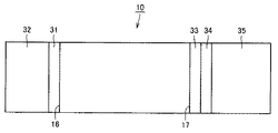
図2に、図1に示す本実施の形態の窒化物半導体レーザ素子の共振器長方向の模式的な側面図を示す。ここで、本実施の形態の窒化物半導体レーザ素子10の光反射側の端面17および光出射部である光出射側の端面16は、たとえば、上記の半導体基板上にバッファ層などの上記の窒化物半導体層を順次積層し、リッジストライプ部を形成した後に、絶縁膜、p電極およびn電極をそれぞれ形成したウエハをダイヤモンドポイントによるスクライブおよびブレークの手法により劈開することによって形成することができる。この劈開による劈開面が図2に示す互いに平行な端面16および端面17となる。
FIG. 2 is a schematic side view of the nitride semiconductor laser element of the present embodiment shown in FIG. 1 in the cavity length direction. Here, the
そして、光出射側の端面16には第1コート膜として厚さ6nmのアルミニウムの酸窒化物膜31が形成され、アルミニウムの酸窒化物膜31上に第2コート膜として厚さ80nmのアルミニウムの酸化物膜32が形成されており、反射率は7%となっている。
An
また、光反射側の端面17には厚さ6nmのアルミニウムの酸窒化物膜33が形成され、アルミニウムの酸窒化物膜33上には厚さ80nmのアルミニウムの酸化物膜34が形成され、アルミニウムの酸化物膜34上には厚さ71nmの酸化シリコン膜と厚さ46nmの酸化チタン膜とを1ペアとして4ペア積層(酸化シリコン膜から積層開始)した後に最表面に厚さ142nmの酸化シリコン膜が積層された反射率95%以上の高反射膜35が形成されている。
Further, an
上記のアルミニウムの酸窒化物膜31、アルミニウムの酸化物膜32、アルミニウムの酸窒化物膜33、アルミニウムの酸化物膜34および高反射膜35はそれぞれ、たとえば以下に説明するECR(Electron Cyclotron Resonance)スパッタリング法により形成することができるが、他の各種スパッタリング法、EB(Electron Beam)蒸着法またはCVD(Chemical Vapor Deposition)法などにより形成することもできる。
The
図3に、ECRスパッタリング装置の一例の模式的な構成図を示す。ここで、ECRスパッタリング装置40は、大きく分けて、成膜炉50とプラズマ生成室60とから構成されている。成膜炉50にはガス導入口51およびガス排気口56が設置されており、成膜炉50内にはターゲット52、加熱用ヒータ53、試料台54およびシャッタ55が設置されている。また、試料台54上には上記劈開後の試料66が設置されており、試料66は端面16または端面17に成膜を行なうことができる向きでホルダ(図示せず)に取り付けられている。また、ガス排気口56には真空ポンプ(図示せず)が取り付けられており、ここから成膜炉50内のガスを排気することができる。また、ターゲット52にはRF電源57が接続されている。
FIG. 3 shows a schematic configuration diagram of an example of an ECR sputtering apparatus. Here, the
また、プラズマ生成室60にはガス導入口61およびマイクロ波導入口62が設置されており、プラズマ生成室60内にはマイクロ波導入窓63および磁気コイル64が設置されている。そして、マイクロ波導入口62から導入されたマイクロ波65がマイクロ波導入窓63を経て導入されることにより、ガス導入口61から導入されたガスからプラズマが生成される。
In addition, a
このような構成のECRスパッタリング装置40を用いて、まず、図2に示す光出射側の端面16に厚さ6nmのアルミニウムの酸窒化物膜31を形成し、引き続き、アルミニウムの酸窒化物膜31上に厚さ80nmのアルミニウムの酸化物膜32を形成する。
Using the
具体的には、まず、成膜炉50内に窒素ガスを5.5sccmの流量で導入し、酸素ガスを1.5sccmの流量で導入し、さらに、プラズマを効率よく発生させて成膜速度を大きくするためにアルゴンガスを20.0sccmの流量で導入する。次に、アルミニウムからなるターゲット52をスパッタリングするためにターゲット52にRFパワーを500W印加し、プラズマの生成に必要なマイクロ波パワーを500W印加したところ、成膜レートが1.7Å/秒で、波長405nmの光の屈折率が2.1、酸素含有量が20原子%であるアルミニウムの酸窒化物膜31を形成することができる。なお、アルミニウムの酸窒化物膜31中を構成するアルミニウム、窒素および酸素の含有量(原子%)はたとえばAES(Auger Electron Spectroscopy)によって測定することができる。また、TEM−EDX(Transmission Electron Microscopy-Energy Dispersive X-ray Spectroscopy)によっても測定することができる。
Specifically, first, nitrogen gas is introduced into the
続いて、窒素ガスの導入を停止し、酸素ガスを6.6sccmの流量で導入し、アルゴンガスを40.0sccmの流量で導入して、アルミニウムからなるターゲット52をスパッタリングするためにターゲット52にRFパワーを500W印加し、プラズマの生成に必要なマイクロ波パワーを500W印加したところ、成膜レートが3.0Å/秒でアルミニウムの酸化物膜32を形成することができる。
Subsequently, the introduction of nitrogen gas is stopped, oxygen gas is introduced at a flow rate of 6.6 sccm, argon gas is introduced at a flow rate of 40.0 sccm, and RF is applied to the
なお、アルミニウムの酸窒化物膜31を形成する前に成膜装置内において端面16をたとえば100℃以上500℃以下の温度で加熱することによって、端面16に付着している酸化膜や不純物などを除去してクリーニングすることが好ましいが、本発明においては特に行なわなくてもよい。また、アルミニウムの酸窒化物膜31を形成する前の端面16にたとえばアルゴンまたは窒素のプラズマを照射することで端面16のクリーニングを行なってもよいが、本発明においては特に行なわなくてもよい。また、アルミニウムの酸窒化物膜31を形成する前の端面16を加熱しながらプラズマ照射することも可能である。また、上記のプラズマの照射に関しては、たとえば、アルゴンのプラズマを照射した後に続けて窒素のプラズマを照射することも可能であり、その逆の順番でプラズマを照射してもよい。アルゴンと窒素以外にも、たとえば、ヘリウム、ネオン、キセノンまたはクリプトンなどの希ガスを用いることもできる。また、端面16に形成されるアルミニウムの酸窒化物膜31の形成についても、たとえば100℃以上500℃以下の温度で加熱した状態で行なうことが好ましいが、本発明においては特に加熱をしない状態でアルミニウムの酸窒化物膜31を形成してもよい。
Before the
また、本発明において、アルミニウムの酸窒化物膜31の上に形成される酸化物膜は酸窒化物膜の形成方法とは異なる方法で形成してもよく、たとえば、アルミニウムの酸窒化物膜31をECRスパッタリング法で形成した後、アルミニウムの酸化物膜32をEB(Electron Beam)蒸着法などにより形成してもよい。
In the present invention, the oxide film formed on the
続いて、上記のアルミニウムの酸窒化物膜31およびアルミニウムの酸化物膜32の形成後は、上記のECRスパッタリング法などにより光反射側の端面17にアルミニウムの酸窒化物膜33、アルミニウムの酸化物膜34および高反射膜35をこの順序で形成する。また、これらの膜の形成前にも加熱によるクリーニングおよび/またはプラズマ照射によるクリーニングを行なうことが好ましい。
Subsequently, after the formation of the
ただし、劣化が問題となるのは光出射側の端面の一部である光出射部であり、光反射側の端面は光出射側に比べて光密度が小さいために劣化が問題とならない場合が多い。したがって、本発明においては、光反射側の端面に形成される膜の構成は特に限定されず、光反射側の端面には膜を形成しなくてもよい。 However, deterioration is a problem in the light emitting part which is a part of the end surface on the light emitting side, and the end surface on the light reflecting side has a light density lower than that on the light emitting side, so deterioration may not be a problem. Many. Therefore, in the present invention, the configuration of the film formed on the end surface on the light reflection side is not particularly limited, and the film may not be formed on the end surface on the light reflection side.
また、光出射側の端面および光反射側の端面に上記の膜を形成した後には加熱処理を行なってもよい。これにより、上記の膜に含まれる水分の除去や加熱処理による膜質の向上を期待することができる。加熱処理の方法としては、ヒータ加熱や紫外などのレーザ照射が可能である。 Further, heat treatment may be performed after the film is formed on the end face on the light emitting side and the end face on the light reflecting side. As a result, it is possible to expect an improvement in film quality due to the removal of moisture contained in the film and the heat treatment. As a heat treatment method, heater heating or laser irradiation such as ultraviolet rays can be performed.
以上のようにして、上記の試料の光出射側の端面16にアルミニウムの酸窒化物膜31およびアルミニウムの酸化物膜32を順次形成し、光反射側の端面17にアルミニウムの酸窒化物膜33、アルミニウムの酸化物膜34および高反射膜35を順次形成した後にチップ状に分割することによって窒化物半導体レーザ素子が得られる。
As described above, the
このようにして得られた本実施の形態の窒化物半導体レーザ素子について70℃の温度環境下でCW駆動して光出力が100mWのレーザ光を連続発振させることによりエージング試験を行なった。その結果を図4に示す。図4に示すように、本実施の形態の窒化物半導体レーザ素子は、500時間が経過しても、エージング試験を行なった7個の窒化物半導体レーザ素子すべてがレーザ光の発振を停止することなく駆動している。 The nitride semiconductor laser device of the present embodiment thus obtained was subjected to an aging test by CW driving in a temperature environment of 70 ° C. to continuously oscillate a laser beam having an optical output of 100 mW. The result is shown in FIG. As shown in FIG. 4, in the nitride semiconductor laser element of this embodiment, all of the seven nitride semiconductor laser elements subjected to the aging test stop oscillation of the laser beam even after 500 hours have elapsed. Driving without.
比較のために、光出射側のアルミニウムの酸化物膜32および光反射側のアルミニウムの酸化物膜34の厚さをそれぞれ40nmとしたこと以外は本実施の形態と同様にして窒化物半導体レーザ素子を作製した。そして、このようにして得られた比較のための窒化物半導体レーザ素子について本実施の形態の窒化物半導体レーザ素子と同様にしてエージング試験を行なった。その結果を図5に示す。図5に示すように、比較のための窒化物半導体レーザ素子についてはエージング試験を行なった6個の窒化物半導体レーザ素子すべてが60時間以内に発振停止している。これらの発振停止した窒化物半導体レーザ素子の光出射側の端面を観察すると、熱で融解したと思われる穴が形成されていた。
For comparison, the nitride semiconductor laser device is the same as the present embodiment except that the thickness of the light emitting side
さらに、比較のために、光出射側のアルミニウムの酸窒化物膜31および光反射側のアルミニウムの酸窒化物膜33の厚さをそれぞれ3nmとしたこと以外は本実施の形態と同様にして窒化物半導体レーザ素子を作製した。そして、このようにして得られた比較のための窒化物半導体レーザ素子について70℃の温度環境下でCW駆動して光出力が65mWの低出力のレーザ光を連続発振させることによりエージング試験を行なった。その結果を図6に示す。図6に示すように、この比較のための窒化物半導体レーザ素子についてはエージング試験を行なった10個の窒化物半導体レーザ素子すべてが400時間まで発振停止することなく正常に駆動している。
Further, for comparison, nitriding is performed in the same manner as in the present embodiment except that the thickness of the
しかしながら、この窒化物半導体レーザ素子について、70℃の温度環境下でCW駆動して光出力が100mWの高出力のレーザ光を連続発振させることによりエージング試験を行なったところ、図7に示すように、エージング試験を行なった7個の窒化物半導体レーザ素子すべてが20時間以内に発振停止している。これらの発振停止した窒化物半導体レーザ素子の光出射部を観察すると、熱で融解したと思われる穴が形成されていた。 However, this nitride semiconductor laser device was subjected to an aging test by CW driving in a temperature environment of 70 ° C. and continuously oscillating a high-power laser beam having an optical output of 100 mW, as shown in FIG. All of the seven nitride semiconductor laser elements subjected to the aging test stopped oscillation within 20 hours. When observing the light emitting portion of the nitride semiconductor laser element whose oscillation was stopped, a hole that seemed to have been melted by heat was formed.
一方、上記のエージング試験を500時間行なった後の本実施の形態の窒化物半導体レーザ素子についても光出射部の劣化を調査したが、劣化は確認されなかった。 On the other hand, the nitride semiconductor laser element of the present embodiment after the above aging test for 500 hours was also examined for deterioration of the light emitting portion, but no deterioration was confirmed.
したがって、CW駆動で光出力が65mW程度の低出力であれば、光出射側のアルミニウムの酸窒化物膜31の厚さが3nmと薄い場合であっても十分な長期信頼性が得られるが、CW駆動で光出力が100mW程度の高出力となると長期的な信頼性が得られないということがわかった。
Therefore, if the light output is a low output of about 65 mW by CW driving, sufficient long-term reliability can be obtained even when the thickness of the
なお、比較のための窒化物半導体レーザ素子について、CW駆動で光出力が65mWの低出力駆動のエージング試験で長期的な信頼性が得られたのは、アルミニウムの酸窒化膜が密着層として機能し、光出射側の端面との密着性が良好であったためと考えられる。しかしながら、CW駆動で光出力が100mWという高出力駆動時においては、アルミニウムの酸窒化膜が単に密着層として機能するだけでは不十分といえる。 In addition, the nitride semiconductor laser device for comparison has long-term reliability in the low-power driving aging test with a light output of 65 mW by CW driving. The aluminum oxynitride film functions as an adhesion layer. However, it is considered that the adhesion with the end surface on the light emission side was good. However, it can be said that the aluminum oxynitride film does not simply function as an adhesion layer when the optical output is 100 mW with CW drive.
以上から、アルミニウムの酸窒化物膜31の厚さを6nm、かつ、アルミニウムの酸化物膜の厚さを80nmとすることによって、高出力駆動時において光出射部の劣化を原因とする信頼性不良の発生を低減することができ、高出力駆動時の長期的な信頼性を改善することができることがわかった。
From the above, by setting the thickness of the
つまり、光出射部に形成されるアルミニウムの酸窒化物膜31の厚さとアルミニウムの酸化物膜32の厚さを十分に厚くすることで、これらの膜の厚さが薄い場合には不十分であった高出力駆動時の長期的な信頼性を得ることができる。
That is, by sufficiently increasing the thickness of the
次に、高出力駆動時の長期的な信頼性を得るために必要な厚さを調査するために、アルミニウムの酸窒化物膜31とアルミニウムの酸化物膜32の厚さを変えてエージング試験を行なった。
Next, in order to investigate the thickness necessary for obtaining long-term reliability at the time of high output driving, an aging test is performed by changing the thicknesses of the
図8に、本実施の形態の窒化物半導体レーザ素子の光出射側の端面のアルミニウムの酸窒化物膜31の厚さを6nmに固定し、アルミニウムの酸窒化物膜31上に形成されるアルミニウムの酸化物膜32の厚さを変化させて、70℃の温度環境下でCW駆動して光出力が100mWの高出力のレーザ光を連続発振させたときに500時間後に正常に駆動している窒化物半導体レーザ素子の割合とアルミニウムの酸化物膜32の厚さとの関係を示す。
In FIG. 8, the thickness of the
図8に示すように、光出射側の端面のアルミニウムの酸窒化物膜31の厚さが6nmである場合には、アルミニウムの酸窒化物膜31上に形成されるアルミニウムの酸化物膜32の厚さが80nm以上である場合には高出力駆動時においても長期的な信頼性を得ることができることが確認された。
As shown in FIG. 8, when the thickness of the
次に、アルミニウムの酸化物膜32の厚さをそれぞれ80nm、160nmおよび240nmとし、70℃の温度環境下でCW駆動して光出力が100mWの高出力のレーザ光を500時間連続発振させたときのCODレベルを比較した。その結果、それぞれの厚さについて5個の窒化物半導体レーザ素子のCODレベルの平均は、アルミニウムの酸化物膜32の厚さが80nmのときに258mW、160nmのときに340mW、240nmのときに346mWであった。したがって、アルミニウムの酸化物膜32の厚さは80nm以上であることが好ましく、160nm以上であることがより好ましいことが確認された。
Next, when the thickness of the
続いて、図9に、本実施の形態の窒化物半導体レーザ素子の光出射側の端面のアルミニウムの酸窒化物膜31の厚さを変化させ、アルミニウムの酸窒化物膜31上に形成されるアルミニウムの酸化物膜32の厚さを80nmに固定して、70℃の温度環境下でCW駆動して光出力が100mWの高出力のレーザ光を連続発振させたときに500時間後に正常に駆動している窒化物半導体レーザ素子の割合とアルミニウムの酸窒化物膜31の厚さとの関係を示す。
9, the thickness of the
図9に示すように、光出射側の端面のアルミニウムの酸化物膜32の厚さが80nmである場合には、アルミニウムの酸窒化物膜31の厚さを6nm以上としたときに高出力駆動時においても長期的な信頼性を得ることができることが確認された。
As shown in FIG. 9, when the thickness of the
次に、アルミニウムの酸窒化物膜31の厚さをそれぞれ6nm、12nmおよび50nmとし、70℃の温度環境下でCW駆動して光出力が100mWの高出力のレーザ光を500時間連続発振させたときのCODレベルを比較した。その結果、それぞれの厚さについて5個の窒化物半導体レーザ素子のCODレベルの平均は、アルミニウムの酸窒化物膜31の厚さが6nmのときに258mW、12nmのときに356mW、50nmのときに487mWであった。したがって、アルミニウムの酸窒化物膜31の厚さは6nm以上であることが好ましく、12nm以上であることがより好ましく、50nm以上であることがさらに好ましいことが確認された。
Next, the thickness of the
以上の結果を考慮すると、アルミニウムの酸窒化物膜31の厚さが6nm以上であり、かつ、その上のアルミニウムの酸化物膜32の厚さが80nm以上である場合には、高出力駆動時においても光出射部の劣化を引き起こすことなく長期的な信頼性が得られると考えられる。
In consideration of the above results, when the thickness of the
(実施の形態2)
本実施の形態の窒化物半導体レーザ素子は、光出射側および光反射側の端面に形成される膜の構成を変更したことならびに発振されるレーザ光の波長を410nmとしたこと以外は、実施の形態1の窒化物半導体レーザ素子と同様の構成を有している。
(Embodiment 2)
The nitride semiconductor laser device according to the present embodiment is implemented except that the configuration of the film formed on the end faces on the light emitting side and the light reflecting side is changed and the wavelength of the oscillated laser light is 410 nm. The structure is the same as that of the nitride semiconductor laser element of mode 1.
ここで、本実施の形態の窒化物半導体レーザ素子においては、光出射側および光反射側の端面にそれぞれ厚さ6nmのアルミニウムの窒化物膜を形成し、それぞれのアルミニウムの窒化物膜上に厚さ80nmのアルミニウムの酸化物膜が形成されている。なお、光出射側の反射率は7%に設定されている。なお、アルミニウムの窒化物膜およびアルミニウムの酸化物膜はECRスパッタリング法で形成している。具体的には、実施の形態1でアルミニウムの酸窒化物膜を形成する際に導入した酸素ガスを導入することなく成膜を行なった。アルミニウムの窒化物膜は他にも各種スパッタ法やMBE(Molecular Beam Epitaxy)法などで形成することが可能である。また、光反射側の端面においては、アルミニウムの酸化物膜上に実施の形態1と同一の構成の高反射膜が形成されている。 Here, in the nitride semiconductor laser element of the present embodiment, an aluminum nitride film having a thickness of 6 nm is formed on each of the end surfaces on the light emitting side and the light reflecting side, and the thickness is formed on each aluminum nitride film. An 80 nm thick aluminum oxide film is formed. The reflectance on the light exit side is set to 7%. The aluminum nitride film and the aluminum oxide film are formed by ECR sputtering. Specifically, the film formation was performed without introducing the oxygen gas introduced when forming the aluminum oxynitride film in the first embodiment. The aluminum nitride film can be formed by various other sputtering methods or MBE (Molecular Beam Epitaxy) methods. In addition, a high reflection film having the same configuration as that of the first embodiment is formed on the aluminum oxide film on the end surface on the light reflection side.
本実施の形態の窒化物半導体レーザ素子について、実施の形態1と同一の方法および同一の条件でエージング試験を行なった。その結果を図10に示す。図10に示すように、エージング試験を行なった14個の本実施の形態の窒化物半導体レーザ素子すべてが200時間が経過しても、レーザ光の発振を停止することなく駆動していることが確認され、高出力駆動時の長期的な信頼性が得られることがわかった。 An aging test was performed on the nitride semiconductor laser element of the present embodiment under the same method and the same conditions as in the first embodiment. The result is shown in FIG. As shown in FIG. 10, all of the 14 nitride semiconductor laser elements of the present embodiment subjected to the aging test are driven without stopping the oscillation of the laser beam even after 200 hours have passed. It was confirmed that long-term reliability at the time of high output drive was obtained.
(実施の形態3)
本実施の形態の窒化物半導体レーザ素子は、光出射側および光反射側の端面に形成される膜の構成を変更したことならびに発振されるレーザ光の波長を400nmとしたこと以外は、実施の形態1の窒化物半導体レーザ素子と同様の構成を有している。
(Embodiment 3)
The nitride semiconductor laser device of the present embodiment is implemented except that the configuration of the film formed on the light emitting side and light reflecting side end faces is changed and the wavelength of the oscillated laser beam is set to 400 nm. The structure is the same as that of the nitride semiconductor laser element of mode 1.
ここで、本実施の形態の窒化物半導体レーザ素子においては、光出射側および光反射側の端面にそれぞれ厚さ12nmのアルミニウムの酸窒化物膜を形成し、それぞれのアルミニウムの窒化物膜上に厚さ80nmのアルミニウムの酸化物膜が形成されている。なお、光出射側の反射率は10%に設定されている。また、光反射側の端面においては、アルミニウムの酸化物膜上に実施の形態1と同一の構成の高反射膜が形成されている。 Here, in the nitride semiconductor laser device of the present embodiment, an aluminum oxynitride film having a thickness of 12 nm is formed on each of the light emitting side and light reflecting side end faces, and the aluminum nitride film is formed on each aluminum nitride film. An aluminum oxide film having a thickness of 80 nm is formed. The reflectance on the light exit side is set to 10%. In addition, a high reflection film having the same configuration as that of the first embodiment is formed on the aluminum oxide film on the end surface on the light reflection side.
本実施の形態の窒化物半導体レーザ素子について、実施の形態1と同一の方法および同一の条件でエージング試験を行なった。その結果を図11に示す。図11に示すように、エージング試験を行なった5個の本実施の形態の窒化物半導体レーザ素子すべてが800時間が経過しても、レーザ光の発振を停止することなく駆動していることが確認され、高出力駆動時の長期的な信頼性が得られることがわかった。 An aging test was performed on the nitride semiconductor laser element of the present embodiment under the same method and the same conditions as in the first embodiment. The result is shown in FIG. As shown in FIG. 11, all of the five nitride semiconductor laser elements of the present embodiment subjected to the aging test are driven without stopping the oscillation of the laser beam even after 800 hours have passed. It was confirmed that long-term reliability at the time of high output drive was obtained.
(実施の形態4)
本実施の形態の窒化物半導体レーザ素子は、光出射側および光反射側の端面に形成される膜の構成を変更したことならびに発振されるレーザ光の波長を390nmとしたこと以外は、実施の形態1の窒化物半導体レーザ素子と同様の構成を有している。
(Embodiment 4)
The nitride semiconductor laser element of the present embodiment is the same as that of the embodiment except that the configuration of the film formed on the end faces on the light emitting side and the light reflecting side is changed and the wavelength of the oscillated laser light is 390 nm. The structure is the same as that of the nitride semiconductor laser element of mode 1.
ここで、本実施の形態の窒化物半導体レーザ素子においては、光出射側および光反射側の端面にそれぞれ厚さ50nmのアルミニウムの酸窒化物膜を形成し、それぞれのアルミニウムの窒化物膜上に厚さ160nmのアルミニウムの酸化物膜が形成されている。なお、光出射側の反射率は6%である。また、光反射側の端面においては、アルミニウムの酸化物膜上に実施の形態1と同一の構成の高反射膜が形成されている。 Here, in the nitride semiconductor laser device of the present embodiment, an aluminum oxynitride film having a thickness of 50 nm is formed on each of the light emitting side and light reflecting side end faces, and the aluminum nitride film is formed on each aluminum nitride film. An aluminum oxide film having a thickness of 160 nm is formed. Note that the reflectance on the light exit side is 6%. In addition, a high reflection film having the same configuration as that of the first embodiment is formed on the aluminum oxide film on the end surface on the light reflection side.
本実施の形態の窒化物半導体レーザ素子について、実施の形態1と同一の方法および同一の条件でエージング試験を行なった。その結果を図12に示す。図12に示すように、エージング試験を行なった8個の本実施の形態の窒化物半導体レーザ素子すべてが1000時間が経過しても、レーザ光の発振を停止することなく駆動していることが確認され、高出力駆動時の長期的な信頼性を改善することができることがわかった。 An aging test was performed on the nitride semiconductor laser element of the present embodiment under the same method and the same conditions as in the first embodiment. The result is shown in FIG. As shown in FIG. 12, all of the eight nitride semiconductor laser elements according to the present embodiment subjected to the aging test are driven without stopping the oscillation of the laser beam even after 1000 hours have passed. It was confirmed that it was possible to improve long-term reliability when driving at high output.
なお、上記においては、窒化物半導体レーザ素子について高出力駆動時の信頼性について確認したが、窒化物半導体ダイオード素子の光出射部である発光面に上記の第1コート膜および第2コート膜を形成した場合でも上記の結果と同様の結果が得られると考えられる。 In the above description, the reliability at the time of high output driving of the nitride semiconductor laser element has been confirmed. However, the first coat film and the second coat film are applied to the light emitting surface which is the light emitting portion of the nitride semiconductor diode element. Even when formed, it is considered that the same result as the above result can be obtained.
(実施の形態5)
本実施の形態の窒化物半導体レーザ素子は、光出射側および光反射側の端面に形成される膜の構成を変更したこと以外は、実施の形態1の窒化物半導体レーザ素子と同様の構成を有している。
(Embodiment 5)
The nitride semiconductor laser device of the present embodiment has the same configuration as that of the nitride semiconductor laser device of the first embodiment, except that the configuration of the films formed on the end surfaces on the light emitting side and the light reflecting side is changed. Have.
ここで、本実施の形態の窒化物半導体レーザ素子においては、光出射側の端面に厚さ20nmのアルミニウムの酸窒化物膜が形成され、その上に厚さ150nmのアルミニウムの酸化物膜が形成されており、光出射側の端面に形成された膜の反射率は5%となっている。 Here, in the nitride semiconductor laser device of the present embodiment, an aluminum oxynitride film having a thickness of 20 nm is formed on the end face on the light emitting side, and an aluminum oxide film having a thickness of 150 nm is formed thereon. Thus, the reflectance of the film formed on the end face on the light emitting side is 5%.
また、光反射側の端面には、厚さ20nmのアルミニウムの酸窒化物膜が形成され、その上に厚さ110nmのアルミニウムの酸窒化物膜が形成され、その上に、厚さ71nmの酸化シリコン膜と厚さ46nmの酸化チタン膜とを1ペアとして4ペア積層(酸化シリコン膜から積層開始)された後に最表面に厚さ142nmの酸化シリコン膜が形成されており、光反射側の端面に形成された膜の反射率は95%以上となっている。 Further, an aluminum oxynitride film having a thickness of 20 nm is formed on the end face on the light reflection side, an aluminum oxynitride film having a thickness of 110 nm is formed thereon, and an oxidation film having a thickness of 71 nm is formed thereon. A silicon oxide film having a thickness of 142 nm is formed on the outermost surface after four pairs of silicon films and a titanium oxide film having a thickness of 46 nm are laminated as one pair (lamination starts from the silicon oxide film). The reflectance of the film formed in the film is 95% or more.
なお、アルミニウムの酸窒化物膜およびアルミニウムの酸化物膜はそれぞれECRスパッタリング法で形成されている。 The aluminum oxynitride film and the aluminum oxide film are each formed by ECR sputtering.
本実施の形態の窒化物半導体レーザ素子について、実施の形態1と同様にして、70℃の温度環境下でCW駆動して光出力が100mWの高出力のレーザ光を連続発振させることによってエージング試験を行なった。その結果を図14に示す。図14に示すように、エージング試験を行なった4個の本実施の形態の窒化物半導体レーザ素子すべてが2500時間が経過しても、レーザ光の発振を停止することなく駆動していることが確認され、高出力駆動時の長期的な信頼性が得られることがわかった。 For the nitride semiconductor laser device of the present embodiment, as in the first embodiment, an aging test is performed by continuously oscillating a high-power laser beam having a light output of 100 mW by CW driving in a temperature environment of 70 ° C. Was done. The result is shown in FIG. As shown in FIG. 14, all of the four nitride semiconductor laser elements according to the present embodiment subjected to the aging test are driven without stopping the oscillation of the laser beam even after 2500 hours. It was confirmed that long-term reliability at the time of high output drive was obtained.
また、本実施の形態の窒化物半導体レーザ素子について、70℃の温度環境下でCW駆動して光出力が100mWの高出力のレーザ光を500時間連続発振させたときのCODレベルを測定したところ、5個の窒化物半導体レーザ素子のCODレベルの平均は338mWであった。 Further, with respect to the nitride semiconductor laser device of the present embodiment, the COD level was measured when CW driving was performed in a temperature environment of 70 ° C. and a high-power laser beam having an optical output of 100 mW was continuously oscillated for 500 hours. The average of the COD levels of the five nitride semiconductor laser elements was 338 mW.
また、実施の形態1で述べたように、光出射側の端面のアルミニウムの酸窒化物膜上のアルミニウムの酸化物膜の厚さが80nmのときに258mW、160nmのときに340mW、240nmのときに346mWであったことから、光出射側の端面のアルミニウムの酸窒化物膜上のアルミニウムの酸化物膜の厚さが150nm以上の場合には80nmのときよりも高出力駆動時の長期的な信頼性を大きく改善することができるといえる。 Further, as described in the first embodiment, when the thickness of the aluminum oxide film on the aluminum oxynitride film on the light emitting side end face is 80 nm, it is 258 mW, 160 nm, 340 mW, 240 nm Therefore, when the thickness of the aluminum oxide film on the aluminum oxynitride film on the end surface on the light emission side is 150 nm or more, the long-term driving at high output is longer than that at 80 nm. It can be said that the reliability can be greatly improved.
(実施の形態6)
本実施の形態の窒化物半導体レーザ素子は、光出射側および光反射側の端面に形成される膜の構成を変更したこと以外は、実施の形態1の窒化物半導体レーザ素子と同様の構成を有している。
(Embodiment 6)
The nitride semiconductor laser device of the present embodiment has the same configuration as that of the nitride semiconductor laser device of the first embodiment, except that the configuration of the films formed on the end surfaces on the light emitting side and the light reflecting side is changed. Have.
ここで、本実施の形態の窒化物半導体レーザ素子においては、光出射側の端面に厚さ20nmのアルミニウムの酸窒化物膜が形成され、その上に厚さ130nmのアルミニウムの酸化物膜が形成されており、光出射側の端面に形成された膜の反射率は12.5%となっている。 Here, in the nitride semiconductor laser device of the present embodiment, an aluminum oxynitride film having a thickness of 20 nm is formed on the end face on the light emitting side, and an aluminum oxide film having a thickness of 130 nm is formed thereon. The reflectance of the film formed on the end surface on the light emission side is 12.5%.
また、光反射側の端面には、厚さ20nmのアルミニウムの酸窒化物膜が形成され、その上に厚さ110nmのアルミニウムの酸窒化物膜が形成され、その上に、厚さ71nmの酸化シリコン膜と厚さ46nmの酸化チタン膜とを1ペアとして4ペア積層(酸化シリコン膜から積層開始)された後に最表面に厚さ142nmの酸化シリコン膜が形成されており、光反射側の端面に形成された膜の反射率は95%以上となっている。 Further, an aluminum oxynitride film having a thickness of 20 nm is formed on the end face on the light reflection side, an aluminum oxynitride film having a thickness of 110 nm is formed thereon, and an oxidation film having a thickness of 71 nm is formed thereon. A silicon oxide film having a thickness of 142 nm is formed on the outermost surface after four pairs of silicon films and a titanium oxide film having a thickness of 46 nm are laminated as one pair (lamination starts from the silicon oxide film). The reflectance of the film formed in the film is 95% or more.
なお、アルミニウムの酸窒化物膜およびアルミニウムの酸化物膜はそれぞれECRスパッタリング法で形成されている。 The aluminum oxynitride film and the aluminum oxide film are each formed by ECR sputtering.
本実施の形態の窒化物半導体レーザ素子について、実施の形態1と同様にして、70℃の温度環境下でCW駆動して光出力が100mWの高出力のレーザ光を連続発振させることによってエージング試験を行なった。その結果を図15に示す。図15に示すように、エージング試験を行なった8個の本実施の形態の窒化物半導体レーザ素子すべてが1200時間が経過しても、レーザ光の発振を停止することなく駆動していることが確認され、高出力駆動時の長期的な信頼性が得られることがわかった。 For the nitride semiconductor laser device of the present embodiment, as in the first embodiment, an aging test is performed by continuously oscillating a high-power laser beam having a light output of 100 mW by CW driving in a temperature environment of 70 ° C. Was done. The result is shown in FIG. As shown in FIG. 15, all of the eight nitride semiconductor laser elements according to the present embodiment subjected to the aging test are driven without stopping the oscillation of the laser light even after 1200 hours have passed. It was confirmed that long-term reliability at the time of high output drive was obtained.
また、本実施の形態の窒化物半導体レーザ素子について、70℃の温度環境下でCW駆動して光出力が100mWの高出力のレーザ光を500時間連続発振させたときのCODレベルを測定したところ、5個の窒化物半導体レーザ素子のCODレベルの平均は320mWであった。 Further, with respect to the nitride semiconductor laser device of the present embodiment, the COD level was measured when CW driving was performed in a temperature environment of 70 ° C. and a high-power laser beam having an optical output of 100 mW was continuously oscillated for 500 hours. The average of the COD levels of the five nitride semiconductor laser elements was 320 mW.
また、実施の形態1で述べたように、光出射側の端面のアルミニウムの酸窒化物膜上のアルミニウムの酸化物膜の厚さが80nmのときに258mW、130nmのときに338mW、160nmのときに340mW、240nmのときに346mWであったことから、光出射側の端面のアルミニウムの酸窒化物膜上のアルミニウムの酸化物膜の厚さが130nm以上の場合には80nmのときよりも高出力駆動時の長期的な信頼性を大きく改善することができるといえる。 Further, as described in the first embodiment, when the thickness of the aluminum oxide film on the aluminum oxynitride film on the light emitting side end face is 258 mW when the thickness is 80 nm, 338 mW when the thickness is 130 nm, and 160 nm When the thickness of the aluminum oxide film on the aluminum oxynitride film on the light emitting side end face is 130 nm or more, the output is higher than that at 80 nm. It can be said that the long-term reliability during driving can be greatly improved.
今回開示された実施の形態はすべての点で例示であって制限的なものではないと考えられるべきである。本発明の範囲は上記した説明ではなくて特許請求の範囲によって示され、特許請求の範囲と均等の意味および範囲内でのすべての変更が含まれることが意図される。 The embodiment disclosed this time should be considered as illustrative in all points and not restrictive. The scope of the present invention is defined by the terms of the claims, rather than the description above, and is intended to include any modifications within the scope and meaning equivalent to the terms of the claims.
本発明は、たとえば、紫外から緑色領域の波長の光を発振する窒化物半導体レーザ素子およびストライプ幅が数十μmの照明用途に用いられるブロードエリア型の窒化物半導体レーザ素子などに利用することができる。 INDUSTRIAL APPLICABILITY The present invention can be used for, for example, a nitride semiconductor laser element that oscillates light having a wavelength in the ultraviolet to green region and a broad area type nitride semiconductor laser element that is used for illumination applications having a stripe width of several tens of μm. it can.
10 窒化物半導体レーザ素子、11 半導体基板、12 絶縁膜、13 リッジストライプ部、14 p電極、15 n電極、16,17 端面、21 バッファ層、22 n型クラッド層、23 n型ガイド層、24 多重量子井戸活性層、25 保護層、26
p型電流ブロック層、27 p型クラッド層、28 p型コンタクト層、31,33 アルミニウムの酸窒化物膜、32,34 アルミニウムの酸化物膜、35 高反射膜、40 ECRスパッタリング装置、50 成膜炉、51,61 ガス導入口、52 ターゲット、53 加熱用ヒータ、54 試料台、55 シャッタ、56 ガス排気口、57 RF電源、60 プラズマ生成室、62 マイクロ波導入口、63 マイクロ波導入窓、64 磁気コイル、65 マイクロ波、66 試料。
DESCRIPTION OF
p-type current blocking layer, 27 p-type cladding layer, 28 p-type contact layer, 31,33 aluminum oxynitride film, 32,34 aluminum oxide film, 35 highly reflective film, 40 ECR sputtering apparatus, 50 film formation Furnace, 51, 61 Gas inlet, 52 Target, 53 Heater, 54 Sample stage, 55 Shutter, 56 Gas exhaust, 57 RF power source, 60 Plasma generation chamber, 62 Microwave inlet, 63 Microwave inlet window, 64 Magnetic coil, 65 microwave, 66 samples.
Claims (5)
前記コート膜上にアルミニウムの酸化物膜が形成されており、
前記コート膜の厚さが6nm以上200nm以下であって、
前記アルミニウムの酸化物膜の厚さが80nm以上1000nm以下であることを特徴とする、窒化物半導体レーザ素子。 A coat film made of aluminum oxynitride is formed on the light emitting side end face of the resonator,
An aluminum oxide film is formed on the coating film,
The coating film has a thickness of 6 nm to 200 nm,
A nitride semiconductor laser device, wherein the aluminum oxide film has a thickness of 80 nm to 1000 nm.
Priority Applications (6)
| Application Number | Priority Date | Filing Date | Title |
|---|---|---|---|
| JP2007017547A JP5430826B2 (en) | 2006-03-08 | 2007-01-29 | Nitride semiconductor laser device |
| US11/713,760 US7792169B2 (en) | 2006-03-08 | 2007-03-05 | Nitride semiconductor light emitting device |
| CN200710085508.6A CN101034727B (en) | 2006-03-08 | 2007-03-07 | Nitride semiconductor light emitting device |
| US12/805,644 US9190806B2 (en) | 2006-03-08 | 2010-08-11 | Nitride semiconductor light emitting device |
| US14/881,523 US9660413B2 (en) | 2006-03-08 | 2015-10-13 | Nitride semiconductor light emitting device |
| US15/583,176 US20170237230A1 (en) | 2006-03-08 | 2017-05-01 | Nitride semiconductor light emitting device |
Applications Claiming Priority (3)
| Application Number | Priority Date | Filing Date | Title |
|---|---|---|---|
| JP2006062636 | 2006-03-08 | ||
| JP2006062636 | 2006-03-08 | ||
| JP2007017547A JP5430826B2 (en) | 2006-03-08 | 2007-01-29 | Nitride semiconductor laser device |
Publications (3)
| Publication Number | Publication Date |
|---|---|
| JP2007273953A JP2007273953A (en) | 2007-10-18 |
| JP2007273953A5 JP2007273953A5 (en) | 2010-03-11 |
| JP5430826B2 true JP5430826B2 (en) | 2014-03-05 |
Family
ID=38478031
Family Applications (1)
| Application Number | Title | Priority Date | Filing Date |
|---|---|---|---|
| JP2007017547A Active JP5430826B2 (en) | 2006-03-08 | 2007-01-29 | Nitride semiconductor laser device |
Country Status (3)
| Country | Link |
|---|---|
| US (4) | US7792169B2 (en) |
| JP (1) | JP5430826B2 (en) |
| CN (1) | CN101034727B (en) |
Families Citing this family (26)
| Publication number | Priority date | Publication date | Assignee | Title |
|---|---|---|---|---|
| JP2007103814A (en) * | 2005-10-07 | 2007-04-19 | Sharp Corp | Nitride semiconductor light emitting device and its manufacturing method |
| KR100853241B1 (en) * | 2005-12-16 | 2008-08-20 | 샤프 가부시키가이샤 | Nitride Semiconductor Light Emitting Device and Method of Fabricating Nitride Semiconductor Laser Device |
| JP5191650B2 (en) * | 2005-12-16 | 2013-05-08 | シャープ株式会社 | Nitride semiconductor light emitting device and method for manufacturing nitride semiconductor light emitting device |
| JP5004597B2 (en) * | 2006-03-06 | 2012-08-22 | シャープ株式会社 | Nitride semiconductor light emitting device and method for manufacturing nitride semiconductor light emitting device |
| JP5430826B2 (en) | 2006-03-08 | 2014-03-05 | シャープ株式会社 | Nitride semiconductor laser device |
| JP4444304B2 (en) * | 2006-04-24 | 2010-03-31 | シャープ株式会社 | Nitride semiconductor light emitting device and method for manufacturing nitride semiconductor light emitting device |
| US7668218B2 (en) | 2007-02-20 | 2010-02-23 | Nichia Corporation | Nitride semiconductor laser element |
| US7701995B2 (en) | 2007-07-06 | 2010-04-20 | Nichia Corporation | Nitride semiconductor laser element |
| JP5014967B2 (en) * | 2007-12-06 | 2012-08-29 | シャープ株式会社 | Light emitting device and method for manufacturing light emitting device |
| JP5183516B2 (en) * | 2008-02-15 | 2013-04-17 | 三洋電機株式会社 | Semiconductor laser element |
| JP5093686B2 (en) | 2008-08-27 | 2012-12-12 | 富士電機株式会社 | Method for forming protective film for magnetic recording medium |
| JP2010146683A (en) * | 2008-12-22 | 2010-07-01 | Fuji Electric Device Technology Co Ltd | Method of forming protective film, protective film obtained by the method and magnetic recording medium including the protective film |
| KR20100122998A (en) * | 2009-05-14 | 2010-11-24 | 엘지이노텍 주식회사 | Light emitting device and method for fabricating the same |
| US9800017B1 (en) | 2009-05-29 | 2017-10-24 | Soraa Laser Diode, Inc. | Laser device and method for a vehicle |
| US9250044B1 (en) * | 2009-05-29 | 2016-02-02 | Soraa Laser Diode, Inc. | Gallium and nitrogen containing laser diode dazzling devices and methods of use |
| JP4621791B2 (en) * | 2009-06-11 | 2011-01-26 | シャープ株式会社 | Nitride semiconductor laser device |
| JP2011060932A (en) * | 2009-09-09 | 2011-03-24 | Panasonic Corp | Nitride semiconductor light-emitting device |
| KR101221722B1 (en) | 2011-03-04 | 2013-01-11 | 주식회사 엘지화학 | Conductive structure body and method for preparing the same |
| CN102828149A (en) * | 2011-06-13 | 2012-12-19 | 鸿富锦精密工业(深圳)有限公司 | Film-coating member and manufacturing method thereof |
| DE102015116335A1 (en) | 2015-09-28 | 2017-03-30 | Osram Opto Semiconductors Gmbh | Semiconductor laser |
| US10714900B2 (en) * | 2018-06-04 | 2020-07-14 | Ii-Vi Delaware, Inc. | Ex-situ conditioning of laser facets and passivated devices formed using the same |
| US11239637B2 (en) | 2018-12-21 | 2022-02-01 | Kyocera Sld Laser, Inc. | Fiber delivered laser induced white light system |
| US11421843B2 (en) | 2018-12-21 | 2022-08-23 | Kyocera Sld Laser, Inc. | Fiber-delivered laser-induced dynamic light system |
| US11884202B2 (en) | 2019-01-18 | 2024-01-30 | Kyocera Sld Laser, Inc. | Laser-based fiber-coupled white light system |
| US12000552B2 (en) | 2019-01-18 | 2024-06-04 | Kyocera Sld Laser, Inc. | Laser-based fiber-coupled white light system for a vehicle |
| CN112151651A (en) * | 2020-08-21 | 2020-12-29 | 华灿光电(苏州)有限公司 | Ultraviolet light-emitting diode epitaxial wafer and preparation method thereof |
Family Cites Families (55)
| Publication number | Priority date | Publication date | Assignee | Title |
|---|---|---|---|---|
| US14323A (en) * | 1856-02-26 | Improved mode of constructing walls and floors of cellars | ||
| JP2884603B2 (en) | 1989-07-17 | 1999-04-19 | 住友電気工業株式会社 | Semiconductor laser device |
| JPH03142892A (en) | 1989-10-27 | 1991-06-18 | Sharp Corp | Semiconductor laser element |
| US5196958A (en) * | 1989-10-31 | 1993-03-23 | U.S. Philips Corporation | Optical amplifier having gain at two separated wavelengths |
| JP2743106B2 (en) * | 1990-01-12 | 1998-04-22 | アルプス電気株式会社 | Semiconductor laser |
| US5231062A (en) * | 1990-08-09 | 1993-07-27 | Minnesota Mining And Manufacturing Company | Transparent aluminum oxynitride-based ceramic article |
| JPH06291422A (en) * | 1993-04-02 | 1994-10-18 | Canon Inc | Optical semiconductor element |
| JP3184031B2 (en) * | 1993-08-25 | 2001-07-09 | 富士通株式会社 | Optical semiconductor element device and method of manufacturing optical semiconductor device |
| JPH07312459A (en) | 1994-05-16 | 1995-11-28 | Canon Inc | Optical semiconductor element |
| JP3209895B2 (en) | 1995-09-08 | 2001-09-17 | 新日本製鐵株式会社 | Airtight device for large diameter rotating body |
| JPH09194204A (en) | 1995-11-16 | 1997-07-29 | Matsushita Electric Ind Co Ltd | Production of aluminum nitride and light emitting semiconductor device |
| JPH09162496A (en) | 1995-12-12 | 1997-06-20 | Nippon Telegr & Teleph Corp <Ntt> | Semiconductor laser and its manufacture |
| JP3774503B2 (en) * | 1996-04-17 | 2006-05-17 | 日本オプネクスト株式会社 | Semiconductor laser device and manufacturing method thereof |
| US5741724A (en) * | 1996-12-27 | 1998-04-21 | Motorola | Method of growing gallium nitride on a spinel substrate |
| US6486068B2 (en) * | 1998-01-08 | 2002-11-26 | Toyoda Gosei Co., Ltd. | Method for manufacturing group III nitride compound semiconductor laser diodes |
| JP2971435B2 (en) * | 1998-03-30 | 1999-11-08 | 東芝電子エンジニアリング株式会社 | Semiconductor laser and method of manufacturing the same |
| US6249534B1 (en) * | 1998-04-06 | 2001-06-19 | Matsushita Electronics Corporation | Nitride semiconductor laser device |
| JP3430036B2 (en) | 1998-10-29 | 2003-07-28 | 松下電器産業株式会社 | Method for forming thin film and method for manufacturing semiconductor light emitting device |
| US6693935B2 (en) * | 2000-06-20 | 2004-02-17 | Sony Corporation | Semiconductor laser |
| JP4033644B2 (en) | 2000-07-18 | 2008-01-16 | 日亜化学工業株式会社 | Gallium nitride light emitting device |
| US7012283B2 (en) * | 2000-09-21 | 2006-03-14 | Sharp Kabushiki Kaisha | Nitride semiconductor light emitting element and optical device containing it |
| US7053413B2 (en) | 2000-10-23 | 2006-05-30 | General Electric Company | Homoepitaxial gallium-nitride-based light emitting device and method for producing |
| JP2002237648A (en) | 2001-02-13 | 2002-08-23 | Fuji Photo Film Co Ltd | Semiconductor laser element |
| JP4977931B2 (en) | 2001-03-06 | 2012-07-18 | ソニー株式会社 | GaN semiconductor laser manufacturing method |
| JP3849758B2 (en) * | 2001-04-12 | 2006-11-22 | ソニー株式会社 | Semiconductor laser element |
| MY132031A (en) | 2001-05-31 | 2007-09-28 | Nichia Corp | Semiconductor laser element |
| JP2003017745A (en) | 2001-06-29 | 2003-01-17 | Shiro Sakai | Gallium nitride-based light emitting element |
| US7501023B2 (en) * | 2001-07-06 | 2009-03-10 | Technologies And Devices, International, Inc. | Method and apparatus for fabricating crack-free Group III nitride semiconductor materials |
| US7067849B2 (en) * | 2001-07-17 | 2006-06-27 | Lg Electronics Inc. | Diode having high brightness and method thereof |
| US6812152B2 (en) | 2001-08-09 | 2004-11-02 | Comlase Ab | Method to obtain contamination free laser mirrors and passivation of these |
| JP2003078199A (en) * | 2001-09-03 | 2003-03-14 | Fuji Photo Film Co Ltd | Semiconductor laser device |
| JP2003101126A (en) * | 2001-09-27 | 2003-04-04 | Mitsubishi Electric Corp | Semiconductor laser device and method of manufacturing the same |
| JP4097601B2 (en) * | 2001-10-26 | 2008-06-11 | アンモノ・スプウカ・ジ・オグラニチョノン・オドポヴィエドニアウノシツィオン | Nitride semiconductor laser device and manufacturing method thereof |
| JP4236840B2 (en) * | 2001-12-25 | 2009-03-11 | 富士フイルム株式会社 | Semiconductor laser element |
| JP2003332688A (en) * | 2002-03-08 | 2003-11-21 | Toyoda Gosei Co Ltd | Iii nitride based compound semiconductor laser |
| JP3856300B2 (en) * | 2002-03-11 | 2006-12-13 | ソニー株式会社 | Semiconductor laser element |
| US6744076B2 (en) * | 2002-03-14 | 2004-06-01 | The Circle For The Promotion Of Science And Engineering | Single crystalline aluminum nitride film, method of forming the same, base substrate for group III element nitride film, light emitting device and surface acoustic wave device |
| JP4097552B2 (en) * | 2003-03-27 | 2008-06-11 | 三菱電機株式会社 | Semiconductor laser device |
| JP2004327581A (en) * | 2003-04-23 | 2004-11-18 | Mitsubishi Electric Corp | Semiconductor laser equipment |
| JP2005079406A (en) * | 2003-09-01 | 2005-03-24 | Matsushita Electric Ind Co Ltd | Manufacturing method of semiconductor laser |
| US7118813B2 (en) * | 2003-11-14 | 2006-10-10 | Cree, Inc. | Vicinal gallium nitride substrate for high quality homoepitaxy |
| JP2005175111A (en) | 2003-12-10 | 2005-06-30 | Hitachi Ltd | Semiconductor laser and its manufacturing method |
| US7356060B2 (en) * | 2004-03-15 | 2008-04-08 | Matsushita Electric Industrial Co., Ltd. | Semiconductor laser device and method for fabricating the same |
| JP2005340625A (en) | 2004-05-28 | 2005-12-08 | Nichia Chem Ind Ltd | Nitride semiconductor laser device |
| JP2006128475A (en) * | 2004-10-29 | 2006-05-18 | Mitsubishi Electric Corp | Semiconductor laser |
| JP4451371B2 (en) * | 2004-12-20 | 2010-04-14 | シャープ株式会社 | Nitride semiconductor laser device |
| JP5285835B2 (en) | 2005-07-13 | 2013-09-11 | 株式会社東芝 | Semiconductor device and manufacturing method thereof |
| JP2007095758A (en) * | 2005-09-27 | 2007-04-12 | Matsushita Electric Ind Co Ltd | Semiconductor laser |
| TW200717843A (en) * | 2005-10-19 | 2007-05-01 | Epistar Corp | Light-emitting element with high-light-extracting-efficiency |
| KR100853241B1 (en) * | 2005-12-16 | 2008-08-20 | 샤프 가부시키가이샤 | Nitride Semiconductor Light Emitting Device and Method of Fabricating Nitride Semiconductor Laser Device |
| JP4776514B2 (en) * | 2005-12-16 | 2011-09-21 | シャープ株式会社 | Nitride semiconductor laser device |
| JP2007201373A (en) | 2006-01-30 | 2007-08-09 | Sharp Corp | Semiconductor laser device |
| JP5004597B2 (en) * | 2006-03-06 | 2012-08-22 | シャープ株式会社 | Nitride semiconductor light emitting device and method for manufacturing nitride semiconductor light emitting device |
| JP5430826B2 (en) | 2006-03-08 | 2014-03-05 | シャープ株式会社 | Nitride semiconductor laser device |
| JP4444304B2 (en) * | 2006-04-24 | 2010-03-31 | シャープ株式会社 | Nitride semiconductor light emitting device and method for manufacturing nitride semiconductor light emitting device |
-
2007
- 2007-01-29 JP JP2007017547A patent/JP5430826B2/en active Active
- 2007-03-05 US US11/713,760 patent/US7792169B2/en active Active
- 2007-03-07 CN CN200710085508.6A patent/CN101034727B/en active Active
-
2010
- 2010-08-11 US US12/805,644 patent/US9190806B2/en active Active
-
2015
- 2015-10-13 US US14/881,523 patent/US9660413B2/en active Active
-
2017
- 2017-05-01 US US15/583,176 patent/US20170237230A1/en not_active Abandoned
Also Published As
| Publication number | Publication date |
|---|---|
| CN101034727A (en) | 2007-09-12 |
| US20170237230A1 (en) | 2017-08-17 |
| CN101034727B (en) | 2014-01-29 |
| US9190806B2 (en) | 2015-11-17 |
| US7792169B2 (en) | 2010-09-07 |
| US20070210324A1 (en) | 2007-09-13 |
| US9660413B2 (en) | 2017-05-23 |
| JP2007273953A (en) | 2007-10-18 |
| US20100308360A1 (en) | 2010-12-09 |
| US20160036197A1 (en) | 2016-02-04 |
Similar Documents
| Publication | Publication Date | Title |
|---|---|---|
| JP5430826B2 (en) | Nitride semiconductor laser device | |
| JP5191650B2 (en) | Nitride semiconductor light emitting device and method for manufacturing nitride semiconductor light emitting device | |
| US7820542B2 (en) | Nitride semiconductor light-emitting device and method for fabrication thereof | |
| JP4444304B2 (en) | Nitride semiconductor light emitting device and method for manufacturing nitride semiconductor light emitting device | |
| JP5004597B2 (en) | Nitride semiconductor light emitting device and method for manufacturing nitride semiconductor light emitting device | |
| JP2010068007A (en) | Nitride semiconductor laser device | |
| JP2012039164A (en) | Nitride semiconductor luminous element, and method for manufacturing nitride semiconductor luminous element | |
| JP2011060932A (en) | Nitride semiconductor light-emitting device | |
| JP4776514B2 (en) | Nitride semiconductor laser device | |
| US8541796B2 (en) | Nitride semiconductor light emitting device and method of fabricating nitride semiconductor laser device | |
| JP4671849B2 (en) | Manufacturing method of nitride semiconductor laser device | |
| JP4689502B2 (en) | Nitride semiconductor laser device | |
| JP4860210B2 (en) | Nitride semiconductor laser device and manufacturing method thereof | |
| JP4799339B2 (en) | Nitride semiconductor light emitting device | |
| JP4066317B2 (en) | Semiconductor laser device, manufacturing method thereof, and optical disc apparatus | |
| JP5431441B2 (en) | Nitride semiconductor light emitting device | |
| JP2007173581A (en) | Method of manufacturing nitride semiconductor laser device | |
| JP5766659B2 (en) | Nitride semiconductor light emitting device | |
| JP2008263247A (en) | Nitride semiconductor light emitting device, and method of manufacturing nitride semiconductor light emitting device |
Legal Events
| Date | Code | Title | Description |
|---|---|---|---|
| A521 | Request for written amendment filed |
Free format text: JAPANESE INTERMEDIATE CODE: A523 Effective date: 20100127 |
|
| A621 | Written request for application examination |
Free format text: JAPANESE INTERMEDIATE CODE: A621 Effective date: 20100127 |
|
| A977 | Report on retrieval |
Free format text: JAPANESE INTERMEDIATE CODE: A971007 Effective date: 20110921 |
|
| A131 | Notification of reasons for refusal |
Free format text: JAPANESE INTERMEDIATE CODE: A131 Effective date: 20120925 |
|
| A521 | Request for written amendment filed |
Free format text: JAPANESE INTERMEDIATE CODE: A523 Effective date: 20121121 |
|
| A02 | Decision of refusal |
Free format text: JAPANESE INTERMEDIATE CODE: A02 Effective date: 20121211 |
|
| A521 | Request for written amendment filed |
Free format text: JAPANESE INTERMEDIATE CODE: A523 Effective date: 20130308 |
|
| A911 | Transfer to examiner for re-examination before appeal (zenchi) |
Free format text: JAPANESE INTERMEDIATE CODE: A911 Effective date: 20130315 |
|
| A912 | Re-examination (zenchi) completed and case transferred to appeal board |
Free format text: JAPANESE INTERMEDIATE CODE: A912 Effective date: 20130405 |
|
| A521 | Request for written amendment filed |
Free format text: JAPANESE INTERMEDIATE CODE: A523 Effective date: 20131023 |
|
| A61 | First payment of annual fees (during grant procedure) |
Free format text: JAPANESE INTERMEDIATE CODE: A61 Effective date: 20131204 |
|
| R150 | Certificate of patent or registration of utility model |
Free format text: JAPANESE INTERMEDIATE CODE: R150 Ref document number: 5430826 Country of ref document: JP Free format text: JAPANESE INTERMEDIATE CODE: R150 |
|
| S111 | Request for change of ownership or part of ownership |
Free format text: JAPANESE INTERMEDIATE CODE: R313113 |
|
| S531 | Written request for registration of change of domicile |
Free format text: JAPANESE INTERMEDIATE CODE: R313531 |
|
| S111 | Request for change of ownership or part of ownership |
Free format text: JAPANESE INTERMEDIATE CODE: R313113 |
|
| S531 | Written request for registration of change of domicile |
Free format text: JAPANESE INTERMEDIATE CODE: R313531 |
|
| R350 | Written notification of registration of transfer |
Free format text: JAPANESE INTERMEDIATE CODE: R350 |