JP4097601B2 - Nitride semiconductor laser device and manufacturing method thereof - Google Patents
Nitride semiconductor laser device and manufacturing method thereof Download PDFInfo
- Publication number
- JP4097601B2 JP4097601B2 JP2003539145A JP2003539145A JP4097601B2 JP 4097601 B2 JP4097601 B2 JP 4097601B2 JP 2003539145 A JP2003539145 A JP 2003539145A JP 2003539145 A JP2003539145 A JP 2003539145A JP 4097601 B2 JP4097601 B2 JP 4097601B2
- Authority
- JP
- Japan
- Prior art keywords
- nitride semiconductor
- face
- layer
- semiconductor laser
- film
- Prior art date
- Legal status (The legal status is an assumption and is not a legal conclusion. Google has not performed a legal analysis and makes no representation as to the accuracy of the status listed.)
- Expired - Fee Related
Links
Images


Classifications
-
- C—CHEMISTRY; METALLURGY
- C30—CRYSTAL GROWTH
- C30B—SINGLE-CRYSTAL GROWTH; UNIDIRECTIONAL SOLIDIFICATION OF EUTECTIC MATERIAL OR UNIDIRECTIONAL DEMIXING OF EUTECTOID MATERIAL; REFINING BY ZONE-MELTING OF MATERIAL; PRODUCTION OF A HOMOGENEOUS POLYCRYSTALLINE MATERIAL WITH DEFINED STRUCTURE; SINGLE CRYSTALS OR HOMOGENEOUS POLYCRYSTALLINE MATERIAL WITH DEFINED STRUCTURE; AFTER-TREATMENT OF SINGLE CRYSTALS OR A HOMOGENEOUS POLYCRYSTALLINE MATERIAL WITH DEFINED STRUCTURE; APPARATUS THEREFOR
- C30B29/00—Single crystals or homogeneous polycrystalline material with defined structure characterised by the material or by their shape
- C30B29/10—Inorganic compounds or compositions
- C30B29/40—AIIIBV compounds wherein A is B, Al, Ga, In or Tl and B is N, P, As, Sb or Bi
- C30B29/403—AIII-nitrides
-
- H—ELECTRICITY
- H01—ELECTRIC ELEMENTS
- H01S—DEVICES USING THE PROCESS OF LIGHT AMPLIFICATION BY STIMULATED EMISSION OF RADIATION [LASER] TO AMPLIFY OR GENERATE LIGHT; DEVICES USING STIMULATED EMISSION OF ELECTROMAGNETIC RADIATION IN WAVE RANGES OTHER THAN OPTICAL
- H01S5/00—Semiconductor lasers
- H01S5/30—Structure or shape of the active region; Materials used for the active region
-
- B—PERFORMING OPERATIONS; TRANSPORTING
- B82—NANOTECHNOLOGY
- B82Y—SPECIFIC USES OR APPLICATIONS OF NANOSTRUCTURES; MEASUREMENT OR ANALYSIS OF NANOSTRUCTURES; MANUFACTURE OR TREATMENT OF NANOSTRUCTURES
- B82Y20/00—Nanooptics, e.g. quantum optics or photonic crystals
-
- C—CHEMISTRY; METALLURGY
- C30—CRYSTAL GROWTH
- C30B—SINGLE-CRYSTAL GROWTH; UNIDIRECTIONAL SOLIDIFICATION OF EUTECTIC MATERIAL OR UNIDIRECTIONAL DEMIXING OF EUTECTOID MATERIAL; REFINING BY ZONE-MELTING OF MATERIAL; PRODUCTION OF A HOMOGENEOUS POLYCRYSTALLINE MATERIAL WITH DEFINED STRUCTURE; SINGLE CRYSTALS OR HOMOGENEOUS POLYCRYSTALLINE MATERIAL WITH DEFINED STRUCTURE; AFTER-TREATMENT OF SINGLE CRYSTALS OR A HOMOGENEOUS POLYCRYSTALLINE MATERIAL WITH DEFINED STRUCTURE; APPARATUS THEREFOR
- C30B29/00—Single crystals or homogeneous polycrystalline material with defined structure characterised by the material or by their shape
- C30B29/10—Inorganic compounds or compositions
- C30B29/40—AIIIBV compounds wherein A is B, Al, Ga, In or Tl and B is N, P, As, Sb or Bi
- C30B29/403—AIII-nitrides
- C30B29/406—Gallium nitride
-
- C—CHEMISTRY; METALLURGY
- C30—CRYSTAL GROWTH
- C30B—SINGLE-CRYSTAL GROWTH; UNIDIRECTIONAL SOLIDIFICATION OF EUTECTIC MATERIAL OR UNIDIRECTIONAL DEMIXING OF EUTECTOID MATERIAL; REFINING BY ZONE-MELTING OF MATERIAL; PRODUCTION OF A HOMOGENEOUS POLYCRYSTALLINE MATERIAL WITH DEFINED STRUCTURE; SINGLE CRYSTALS OR HOMOGENEOUS POLYCRYSTALLINE MATERIAL WITH DEFINED STRUCTURE; AFTER-TREATMENT OF SINGLE CRYSTALS OR A HOMOGENEOUS POLYCRYSTALLINE MATERIAL WITH DEFINED STRUCTURE; APPARATUS THEREFOR
- C30B7/00—Single-crystal growth from solutions using solvents which are liquid at normal temperature, e.g. aqueous solutions
- C30B7/005—Epitaxial layer growth
-
- C—CHEMISTRY; METALLURGY
- C30—CRYSTAL GROWTH
- C30B—SINGLE-CRYSTAL GROWTH; UNIDIRECTIONAL SOLIDIFICATION OF EUTECTIC MATERIAL OR UNIDIRECTIONAL DEMIXING OF EUTECTOID MATERIAL; REFINING BY ZONE-MELTING OF MATERIAL; PRODUCTION OF A HOMOGENEOUS POLYCRYSTALLINE MATERIAL WITH DEFINED STRUCTURE; SINGLE CRYSTALS OR HOMOGENEOUS POLYCRYSTALLINE MATERIAL WITH DEFINED STRUCTURE; AFTER-TREATMENT OF SINGLE CRYSTALS OR A HOMOGENEOUS POLYCRYSTALLINE MATERIAL WITH DEFINED STRUCTURE; APPARATUS THEREFOR
- C30B7/00—Single-crystal growth from solutions using solvents which are liquid at normal temperature, e.g. aqueous solutions
- C30B7/10—Single-crystal growth from solutions using solvents which are liquid at normal temperature, e.g. aqueous solutions by application of pressure, e.g. hydrothermal processes
-
- C—CHEMISTRY; METALLURGY
- C30—CRYSTAL GROWTH
- C30B—SINGLE-CRYSTAL GROWTH; UNIDIRECTIONAL SOLIDIFICATION OF EUTECTIC MATERIAL OR UNIDIRECTIONAL DEMIXING OF EUTECTOID MATERIAL; REFINING BY ZONE-MELTING OF MATERIAL; PRODUCTION OF A HOMOGENEOUS POLYCRYSTALLINE MATERIAL WITH DEFINED STRUCTURE; SINGLE CRYSTALS OR HOMOGENEOUS POLYCRYSTALLINE MATERIAL WITH DEFINED STRUCTURE; AFTER-TREATMENT OF SINGLE CRYSTALS OR A HOMOGENEOUS POLYCRYSTALLINE MATERIAL WITH DEFINED STRUCTURE; APPARATUS THEREFOR
- C30B9/00—Single-crystal growth from melt solutions using molten solvents
-
- H—ELECTRICITY
- H01—ELECTRIC ELEMENTS
- H01S—DEVICES USING THE PROCESS OF LIGHT AMPLIFICATION BY STIMULATED EMISSION OF RADIATION [LASER] TO AMPLIFY OR GENERATE LIGHT; DEVICES USING STIMULATED EMISSION OF ELECTROMAGNETIC RADIATION IN WAVE RANGES OTHER THAN OPTICAL
- H01S5/00—Semiconductor lasers
- H01S5/10—Construction or shape of the optical resonator, e.g. extended or external cavity, coupled cavities, bent-guide, varying width, thickness or composition of the active region
- H01S5/16—Window-type lasers, i.e. with a region of non-absorbing material between the active region and the reflecting surface
- H01S5/164—Window-type lasers, i.e. with a region of non-absorbing material between the active region and the reflecting surface with window regions comprising semiconductor material with a wider bandgap than the active layer
-
- H—ELECTRICITY
- H01—ELECTRIC ELEMENTS
- H01S—DEVICES USING THE PROCESS OF LIGHT AMPLIFICATION BY STIMULATED EMISSION OF RADIATION [LASER] TO AMPLIFY OR GENERATE LIGHT; DEVICES USING STIMULATED EMISSION OF ELECTROMAGNETIC RADIATION IN WAVE RANGES OTHER THAN OPTICAL
- H01S5/00—Semiconductor lasers
- H01S5/30—Structure or shape of the active region; Materials used for the active region
- H01S5/32—Structure or shape of the active region; Materials used for the active region comprising PN junctions, e.g. hetero- or double- heterostructures
- H01S5/3202—Structure or shape of the active region; Materials used for the active region comprising PN junctions, e.g. hetero- or double- heterostructures grown on specifically orientated substrates, or using orientation dependent growth
- H01S5/32025—Structure or shape of the active region; Materials used for the active region comprising PN junctions, e.g. hetero- or double- heterostructures grown on specifically orientated substrates, or using orientation dependent growth non-polar orientation
-
- H—ELECTRICITY
- H01—ELECTRIC ELEMENTS
- H01S—DEVICES USING THE PROCESS OF LIGHT AMPLIFICATION BY STIMULATED EMISSION OF RADIATION [LASER] TO AMPLIFY OR GENERATE LIGHT; DEVICES USING STIMULATED EMISSION OF ELECTROMAGNETIC RADIATION IN WAVE RANGES OTHER THAN OPTICAL
- H01S2304/00—Special growth methods for semiconductor lasers
- H01S2304/12—Pendeo epitaxial lateral overgrowth [ELOG], e.g. for growing GaN based blue laser diodes
-
- H—ELECTRICITY
- H01—ELECTRIC ELEMENTS
- H01S—DEVICES USING THE PROCESS OF LIGHT AMPLIFICATION BY STIMULATED EMISSION OF RADIATION [LASER] TO AMPLIFY OR GENERATE LIGHT; DEVICES USING STIMULATED EMISSION OF ELECTROMAGNETIC RADIATION IN WAVE RANGES OTHER THAN OPTICAL
- H01S5/00—Semiconductor lasers
- H01S5/02—Structural details or components not essential to laser action
- H01S5/0206—Substrates, e.g. growth, shape, material, removal or bonding
- H01S5/021—Silicon based substrates
-
- H—ELECTRICITY
- H01—ELECTRIC ELEMENTS
- H01S—DEVICES USING THE PROCESS OF LIGHT AMPLIFICATION BY STIMULATED EMISSION OF RADIATION [LASER] TO AMPLIFY OR GENERATE LIGHT; DEVICES USING STIMULATED EMISSION OF ELECTROMAGNETIC RADIATION IN WAVE RANGES OTHER THAN OPTICAL
- H01S5/00—Semiconductor lasers
- H01S5/02—Structural details or components not essential to laser action
- H01S5/0206—Substrates, e.g. growth, shape, material, removal or bonding
- H01S5/0213—Sapphire, quartz or diamond based substrates
-
- H—ELECTRICITY
- H01—ELECTRIC ELEMENTS
- H01S—DEVICES USING THE PROCESS OF LIGHT AMPLIFICATION BY STIMULATED EMISSION OF RADIATION [LASER] TO AMPLIFY OR GENERATE LIGHT; DEVICES USING STIMULATED EMISSION OF ELECTROMAGNETIC RADIATION IN WAVE RANGES OTHER THAN OPTICAL
- H01S5/00—Semiconductor lasers
- H01S5/02—Structural details or components not essential to laser action
- H01S5/0206—Substrates, e.g. growth, shape, material, removal or bonding
- H01S5/0218—Substrates comprising semiconducting materials from different groups of the periodic system than the active layer
-
- H—ELECTRICITY
- H01—ELECTRIC ELEMENTS
- H01S—DEVICES USING THE PROCESS OF LIGHT AMPLIFICATION BY STIMULATED EMISSION OF RADIATION [LASER] TO AMPLIFY OR GENERATE LIGHT; DEVICES USING STIMULATED EMISSION OF ELECTROMAGNETIC RADIATION IN WAVE RANGES OTHER THAN OPTICAL
- H01S5/00—Semiconductor lasers
- H01S5/02—Structural details or components not essential to laser action
- H01S5/028—Coatings ; Treatment of the laser facets, e.g. etching, passivation layers or reflecting layers
- H01S5/0281—Coatings made of semiconductor materials
-
- H—ELECTRICITY
- H01—ELECTRIC ELEMENTS
- H01S—DEVICES USING THE PROCESS OF LIGHT AMPLIFICATION BY STIMULATED EMISSION OF RADIATION [LASER] TO AMPLIFY OR GENERATE LIGHT; DEVICES USING STIMULATED EMISSION OF ELECTROMAGNETIC RADIATION IN WAVE RANGES OTHER THAN OPTICAL
- H01S5/00—Semiconductor lasers
- H01S5/20—Structure or shape of the semiconductor body to guide the optical wave ; Confining structures perpendicular to the optical axis, e.g. index or gain guiding, stripe geometry, broad area lasers, gain tailoring, transverse or lateral reflectors, special cladding structures, MQW barrier reflection layers
- H01S5/22—Structure or shape of the semiconductor body to guide the optical wave ; Confining structures perpendicular to the optical axis, e.g. index or gain guiding, stripe geometry, broad area lasers, gain tailoring, transverse or lateral reflectors, special cladding structures, MQW barrier reflection layers having a ridge or stripe structure
-
- H—ELECTRICITY
- H01—ELECTRIC ELEMENTS
- H01S—DEVICES USING THE PROCESS OF LIGHT AMPLIFICATION BY STIMULATED EMISSION OF RADIATION [LASER] TO AMPLIFY OR GENERATE LIGHT; DEVICES USING STIMULATED EMISSION OF ELECTROMAGNETIC RADIATION IN WAVE RANGES OTHER THAN OPTICAL
- H01S5/00—Semiconductor lasers
- H01S5/30—Structure or shape of the active region; Materials used for the active region
- H01S5/32—Structure or shape of the active region; Materials used for the active region comprising PN junctions, e.g. hetero- or double- heterostructures
- H01S5/323—Structure or shape of the active region; Materials used for the active region comprising PN junctions, e.g. hetero- or double- heterostructures in AIIIBV compounds, e.g. AlGaAs-laser, InP-based laser
- H01S5/32308—Structure or shape of the active region; Materials used for the active region comprising PN junctions, e.g. hetero- or double- heterostructures in AIIIBV compounds, e.g. AlGaAs-laser, InP-based laser emitting light at a wavelength less than 900 nm
- H01S5/32341—Structure or shape of the active region; Materials used for the active region comprising PN junctions, e.g. hetero- or double- heterostructures in AIIIBV compounds, e.g. AlGaAs-laser, InP-based laser emitting light at a wavelength less than 900 nm blue laser based on GaN or GaP
-
- H—ELECTRICITY
- H01—ELECTRIC ELEMENTS
- H01S—DEVICES USING THE PROCESS OF LIGHT AMPLIFICATION BY STIMULATED EMISSION OF RADIATION [LASER] TO AMPLIFY OR GENERATE LIGHT; DEVICES USING STIMULATED EMISSION OF ELECTROMAGNETIC RADIATION IN WAVE RANGES OTHER THAN OPTICAL
- H01S5/00—Semiconductor lasers
- H01S5/30—Structure or shape of the active region; Materials used for the active region
- H01S5/34—Structure or shape of the active region; Materials used for the active region comprising quantum well or superlattice structures, e.g. single quantum well [SQW] lasers, multiple quantum well [MQW] lasers or graded index separate confinement heterostructure [GRINSCH] lasers
- H01S5/343—Structure or shape of the active region; Materials used for the active region comprising quantum well or superlattice structures, e.g. single quantum well [SQW] lasers, multiple quantum well [MQW] lasers or graded index separate confinement heterostructure [GRINSCH] lasers in AIIIBV compounds, e.g. AlGaAs-laser, InP-based laser
- H01S5/34333—Structure or shape of the active region; Materials used for the active region comprising quantum well or superlattice structures, e.g. single quantum well [SQW] lasers, multiple quantum well [MQW] lasers or graded index separate confinement heterostructure [GRINSCH] lasers in AIIIBV compounds, e.g. AlGaAs-laser, InP-based laser with a well layer based on Ga(In)N or Ga(In)P, e.g. blue laser
Description
技術分野
本発明は、共振器端面に単結晶AlxGa1−xN(0≦x≦1)からなる端面膜を形成してなる窒化物半導体レーザ素子に関する。
背景技術
従来から広く使用されているGaAs系の半導体を用いた半導体レーザ素子は、その共振器端面に保護膜を形成するウィンドウ構造によってレーザ素子の長寿命化を可能とした。窒化物半導体レーザ素子においても、窒化物半導体はRIE(反応性イオンエッチング)やへき開によって形成された共振器端面はバンドギャップエネルギーが小さいため、出射光の吸収が端面で起こり、この吸収により端面には熱が発生し、100mW以上の高出力レーザを実現するには寿命特性の問題が生じる。このため、窒化物半導体レーザ素子におけるウィンドウ構造を形成することが提案され、保護膜としては、AlGaInN半導体膜を形成する方法(特開平7−249830)、AlN等の保護膜を形成する方法(特開2002−26442)が提案されている。
発明の開示
(発明が解決しようとする技術的課題)
しかしながら、上記に示す保護膜を気相成長法により単結晶で形成するには1000℃以上の成長温度が必要であり、かかる成長温度ではInを含む活性層が損傷を受ける。そのため、この保護膜を活性層が損傷しない温度で形成することになると保護膜はアモルファスとなる。このアモルファスの保護膜を半導体レーザ素子のウィンドウ構造に用いると、単結晶ではないため出射光の散乱が生じ、レーザのビーム形状が均一にならない、またアモルファスは色を持つため光吸収が生じると端面での発熱により端面劣化が起こるという問題点がある。
そこで、本発明は、上記問題を解決するために活性層に損傷を与えない低温で、しかも上記問題の生じない単結晶AlxGa1−xN(0≦x≦1)からなる端面膜を備えた窒化物半導体レーザ素子を提供することを目的とする。
(その解決手段)
本発明に係る窒化物半導体レーザ素子は、n型窒化物半導体層とp型窒化物半導体層との間に、Inを含む窒化物半導体からなる活性層を含む共振器を有する窒化物半導体レーザ素子において、前記レーザ素子の対向する共振器端面の少なくとも出射端面に、前記活性層に損傷を与えない低温で形成され活性層よりバンドギャップエネルギーの大きい単結晶AlxGa1−xN(0≦x≦1)からなる端面膜を有することを特徴とする。
ここで、Inを含む窒化物半導体からなる活性層に損傷を与えない低温とは、Inを含む窒化物半導体からなる活性層の形成温度以下をいう。Inを含む窒化物半導体からなる活性層は通常成長温度900℃で成長させるので、その成長温度以下の温度であれば、上記活性層が分解等により損傷を受けない。したがって、端面膜の成長温度が900℃以下、好ましくは600℃以下、より好ましくは500℃以下であるのがよい。
また、本発明に係る窒化物半導体レーザ素子において、Inを含む窒化物半導体からなる活性層を含む共振器とは光導波領域を言い、通常活性層と光ガイド層により構成される。したがって、本発明における端面膜は少なくとも上記共振器端面領域を覆うように形成されればよい。前記活性層は、少なくとも1つのInGaN井戸層またはInAlGaN井戸層を含み、単一または多重量子井戸構造により構成される。
本発明の端面膜は、単結晶AlxGa1−xN(0≦x≦1)から構成される。この混晶比率は端面膜の機能との関係によって決定される。つまり、活性層の出射端面のバンドギャップエネルギーは出射端面形成時に行うエッチングやへき開によって狭くなっているので、端面膜により該端面のバンドギャップエネルギーを光吸収がなくなるバンドギャップエネルギーまで広げることができるように混晶比が決定される。端面膜の結晶性を考慮すると、Al混晶比は0.3以下、好ましくは0.15以下がよい。本発明に係る窒化物半導体レーザ素子において、前記端面膜の膜厚は50オングストローム以上であることが好ましいが、端面膜の均一性を確保するためには1ミクロン以下、好ましくは2000Åであるのがよい。
本発明では、上記単結晶のAlxGa1−xN(0≦x≦1)を上記低温で形成するためにAMMONO法が適用される。アンモニアの超臨界状態でAlxGa1−xN(0≦x≦1)単結晶層を所定のシード面(本発明ではレーザ素子の共振器端面)に形成する方法であり、AMMONO法の採用により上記単結晶端面膜は900℃以下、好ましくは600℃以下、より好ましくは500℃以下で単結晶端面膜を形成することができる。AMMONO法を採用すると、通常オートクレイブ組成の影響を受け、前記端面膜はNi、Cr、Co、Ti、Fe、Al、Si、Mnから成る群から選ばれる少なくとも1つを含有する場合がある。また前記端面膜はAMMONO法の特徴としてミネラライザーとして使用する族番号1(IUPAC.1989)元素、Li,K、NaまたはCsを少なくとも1つを含有する。前記端面膜が前記窒化物半導体レーザ素子からの出射光を吸収しないため出射端面での熱吸収もなくなり、100mW以上の窒化物半導体レーザ素子においてもCODの発生は抑制される。
また、前記窒化物半導体レーザ素子はGaN基板、サファイア基板、スピネル基板、ZnO基板、SiC基板、その他にはサファイア基板等の異種基板上にGaNの横方向成長により形成したELO成長基板、表面に凹凸を有する窒化物半導体を成長させた基板からなる群より選ばれる基板上に形成される。ここで、ELO(Epitaxial−Lateral−Overgrowth)基板とはGaNの横方向成長を利用した基板であって、転位欠陥を低減させた基板である。超臨界アンモニア中でAlxGa1−xN(0≦x≦1)を端面膜として成長させる本発明においてはGaN基板が好ましい。端面膜と異なる組成の異種基板を使用している窒化物半導体レーザ素子の場合、端面膜の形成中に超臨界アンモニア中に溶解して再結晶する端面膜の半導体中に混在し、不純物となる場合を極力避けるためである。前記GaN基板は超臨界アンモニア中で成長させたGaN基板等である。窒化物半導体と異なる基板上に成長させた窒化物半導体レーザ素子はデバイス工程において、へき開を行うのが困難であった。これは、GaNを成長させる異種基板がへき開性を有しないためである。しかしながら、GaN基板はへき開性を有するため、共振器端面を形成する際に、鏡面を得ることに優れたへき開による端面形成が可能になるからである。且つホモエピタキシャル成長であるから、前記レーザ素子を成長後に基板の反りを抑制できる。これにより、クラックの発生はなくなる。さらに、前記GaN基板は通常レーザ素子を形成する成長面がC面となる。気相成長法により得られるGaN基板を得るからである。AMMONO法によれば、超臨界アンモニア中でGaNのバルク単結晶をC軸方向に厚さ2.5cm以上で成長させた後、カッティングすればφ1インチ以上であってA面やM面を主面としたGaN基板を得ることができる。A面またはM面は極性がない(non−polar)ため、活性層に分極作用を及ぼすことがなくなる。しかも欠陥密度が104/cm2程度またはそれ以下のものが得られる。その他に(000−1)面を主面とするGaN基板を極性転換することでC面である(0001)面を主面とすることができる。
前記窒化物半導体レーザ素子がGaN基板のC面上に形成されると、前記端面膜がM面またはA面上に形成され、極性のない端面膜とすることができる。前記窒化物半導体レーザ素子が超臨界アンモニア中で成長させたGaN基板のA面上に形成されると、レーザ素子の活性層に分極作用を与えず、しかも共振器出射面がM面となり、M面上にM面端面膜が形成され、へき開に有利である。前記窒化物半導体レーザ素子が超臨界アンモニア中で成長させたGaN基板のM面上に形成されると、活性層に分極作用が及ばず、しかも共振器出射面に極性のないA面端面膜を形成することができる。
本発明は、窒化物半導体レーザ素子の製造方法を提供するものであり、n型窒化物半導体層とp型窒化物半導体層との間に、Inを含む窒化物半導体からなる活性層を含む共振器を有する窒化物半導体レーザ素子の製造方法において、前記レーザ素子にエッチング又はへき開を行い対向する共振器端面を形成する第1の工程と、前記レーザ素子の対向する共振器端面の少なくとも出射端面に、前記活性層に損傷を与えない低温で形成される単結晶AlxGa1−xN(0≦x≦1)からなる端面膜を形成する第2の工程とを備えたことを特徴とする。
前記第2の工程は、超臨界アンモニア中で前記端面膜を形成することにより、活性層に損傷を与えない低温で単結晶のAlxGa1−xN(0≦x≦1)とすることができる。
前記第2の工程において、少なくとも共振器のp型コンタクト層の上面に超臨界アンモニアに対して溶解度が端面膜と同等または低いマスクを形成した後、前記端面膜を形成することを特徴とする。このマスクを形成することで溶解性の強い超臨界アンモニア中において窒化物半導体レーザ素子の端面膜形成時にレーザ素子の共振器がp型コンタクト層の上面と端面との角から溶解することを抑制することができる。前記マスクは、酸化ケイ素、窒化ケイ素、窒化アルミニウム、モリブデン、タングステンから成る群から選ばれるのがよい。これらのマスク材は超臨界アンモニア中でGaNに比べて安定であるため、該マスク材で覆われた領域のコンタクト表面では溶解を抑制することができる。マスクは後工程でリッジの形成時には除去が容易である。
前記窒化物半導体レーザ素子の製造方法において、前記端面膜は、超臨界アンモニア中での成膜温度が100℃以上900℃以下である。窒化物半導体レーザ素子は活性層をInGaNを含んだ量子井戸構造をしているため、900℃より高い温度で活性層上に層成長すれば該活性層は分解する恐れがある。本発明によれば、900℃以下、好ましくは600℃以下の温度で端面膜を成長させることができる。
発明を実施するための最良の形態
以下、本発明に係る実施の形態について説明する。
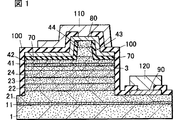
図1は本発明に係る半導体レーザの断面図で、サファイア基板1上にn型窒化物半導体層2とp型窒化物半導体層4とが積層され、その間に、Inを含む窒化物半導体からなる単一、または多重量子井戸構造の活性層3が形成されている。これにより、近紫外から可視光の緑色までの波長領域(370nm以上550nm以下)で発光効率に優れたレーザ素子が得られる。n型窒化物半導体層2は、n−コンタクト層21、クラック防止層22、n型クラッド層23及びn型光ガイド層24とからなる。また、前記クラック防止層22はGaN基板を用いた場合にはウェハーの反りが抑制されるために省略可能となる。p型窒化物半導体層4はキャップ層41、p型光ガイド層42、p型クラッド層43、pコンタクト層44からなる。ここで、前記サファイア基板1上に転位欠陥低減層としてELO層やピット低減を目的としたAlGaN層を介してn−コンタクト層21を形成してもよい。前記上記実施態様では、半導体レーザ素子の共振器は上記活性層3とp型層およびn型層の光ガイド層24,42、またキャップ層41から構成されている。共振器端面の出射端面には、単結晶AlxGa1−xN(0≦x≦1)からなる端面膜5が形成されている。この端面膜は共振器端面の光反射側にも形成すれば(図2)、反射光による端面劣化を抑制することができる。
以下、本実施の形態に係る窒化物半導体レーザ素子の代表的な3つの製造方法を説明する。
図2A〜Dはマスクを形成することなく、端面膜を共振器両端面に設ける工程を示し、
図3A〜Eは共振器の出射端面側以外にマスクを設け、出射端面に端面膜を形成する工程を示し、
図5A〜Eは共振器の出射端面をM面とし、リッジ、電極を形成後にへき開で出射端面を形成する。次に、その端面側以外にマスクを設け、出射端面にM面端面膜を形成し、その後へき開等によりチップ化することでレーザ素子を形成する工程を示す。
図2に示す第1の方法では、まず、サファイア基板1上に700℃以下の低温で成長させたバッファ層11を形成し、そのバッファ層11の上にn型窒化物半導体層2、活性層3及びp型窒化物半導体層4を順次成長させたウェハを準備する(図2A)。ここで、低温バッファ層11上にELO層を介してn型窒化物半導体層2を成長させると欠陥が低減させることができる。
次に、上記ウェハをエッチングによって共振器端面、及びn−コンタクト層21を露出する(図2B)。その後、共振器端面を露出したウェハにAMMONO法を適用して端面膜5を形成する。
オートクレイブ内に端面膜の原料となるフィードストック、反応促進剤となるミネラライザーと共に上記ウエハをセットし、アンモニアを投入し、所定の温度管理を行うことにより超臨界状態とする。
前記ウェハはサファイア基板1にn型窒化物半導体層2、活性層3及びp型窒化物半導体層4を順次成長させたウェハを用いるが、これに代えて、サファイア基板のような異種基板を除去したウェハ、基板1にn型窒化物半導体層2、活性層3及びp型窒化物半導体層4を順次成長させたウェハであって、共振器端面の反射光側のみを超臨界アンモニアに溶解しないか溶解しても端面膜中に混入しない材料、たとえばAg等でマスキング6したウェハ、共振器端面の出射端面以外の全面を前記Ag等でマスキング6したウェハ、前記基板のみをマスキングしたウェハ(図4)を用いることができる。
前記超臨界アンモニア中ではGaNの溶解度も高く、p型窒化物半導体層4の表面にマスクを形成しなければ、最表面と出射端面との角部から窒化物半導体素子が溶解する。そのため、p型窒化物半導体層4の最表面であるp型コンタクト層をマスキングをする。該マスク材は、酸化ケイ素、窒化ケイ素、窒化アルミニウム、モリブデン、タングステンから選ばれる。これらのマスク材は超臨界アンモニア中でGaNに比べて安定であるため、GaNの溶解を抑制することができる。これによりp型コンタクト層上にマスクを形成するとp型コンタクト層と出射端面との角部が溶解するのを抑制できることを意味する。また端面膜を形成した後の工程で除去が容易なものが好ましい。このマスクの膜圧は1μm以上とする。
上記に示したウェハをオートクレイブ内で反応させた後のウェハは窒化物半導体層の露出面に単結晶AlxGa1−xN(0≦x≦1)からなる端面膜を形成している(図2C)。
ついで、p型半導体層4上の端面膜を取り、出射端面に上記保護膜を、反対側には反射膜を形成し、溝部で切り出してレーザ素子を得る。ここで、上記保護膜と反射膜とは同一材料であってもよく、保護作用と反射作用を有するSiO2やTiO2、又はこれらの複数膜で形成される。
図3に示す第2の方法では、まず、GaN基板1のC面上にn型窒化物半導体層2、すなわちn−コンタクト層21、クラック防止層22、n型クラッド層23及びn型光ガイド層24、次いで活性層3、p型窒化物半導体層4、すなわちキャップ層41、p型光ガイド層42、p型クラッド層43、pコンタクト層44を順次成長させたウェハを準備する(図3A)。ここで、GaN基板を使用するので、第1法のように低温バッファ層11上にELO層を介してn型窒化物半導体層2を成長させることなく、エピ層の欠陥を低減させることができる。
次に、上記ウェハをエッチングによって共振器端面、及びn−コンタクト層21を露出し、共振器端面の出射面側を除いてマスク7を形成する(図3B)。その後、共振器端面を露出したウェハにAMMONO法を適用して端面膜5を形成する(図3C)。
次に、端面膜を形成した後、マスク7を取って、通常のデバイス工程によりリッジを形成する(図3D)。光導波を行うリッジストライプは共振器方向に形成される。リッジの幅は1.0〜20μmであって、リッジの深さはp型クラッド層またはp型ガイド層まで到達している。その後、リッジを覆うように、ZrO2膜からなる埋め込み層70を形成する。リッジの最上部のp型コンタクト層43に接触するようにpオーミック電極80を形成する。前記リッジの数は単数だけでなく、複数形成してマルチストライプ型レーザ素子とすることもできる。次に、n型コンタクト層21の表面にn電極90をp電極と平行に形成する。次に、p−パット電極110、n−パッド電極120を形成する。さらに、SiO2とTiO2とを交互に形成しパターンニングすることによりp電極及びn電極の上を除く素子全体を覆うように、SiO2/TiO2絶縁膜をレーザ発振のための反射膜100として機能するように形成する。最後に、ウエハからスクライビングにより、個々の窒化物半導体レーザ素子に分割する。以上のようにして窒化物半導体レーザ素子を作製することができる(図3E,図1)。
また、前記端面膜上に共振を効率よく行うための保護膜を設けてもよい。該保護膜は端面膜であるAlGaNと屈折率差を有するものである。具体的にはNb、Ni、Cr、Ti、Cu、Fe、Zr、Hf、W、Rh、Ru、Mg、Al、Sc、Y、Mo、Ta、Co、Pd、Ag、Au、Pt、Ga、更にはこれらの酸化物、窒化物、フッ化物などの化合物である。
図5A〜Eは第3の方法として、基板としてGaN基板1のA面を用い、出射端面をM面としてへき開によりレーザ素子を得る工程を示す。このGaN基板1上に第2法と同様に窒化物半導体レーザ素子を形成する。同一部材には同一番号を付して説明を省略する。次に、エッチングによりn型コンタクト層21を露出させる(図5A)。その後、リッジを形成し(図5B)、さらにリッジの最上部のp型コンタクト層43に接触するようにpオーミック電極80を形成する。次に、n型コンタクト層21の表面にn電極90を形成する。次に、p−パット電極110、n−パッド電極120を形成する(図5C)。次に、出射端面をへき開により形成する。これにより、ウェハーはバー状になる。その後、超臨界アンモニア中で端面膜5を形成する(図5D)。これをへき開してレーザ素子を作製することができる(図5E)。
超臨界アンモニアを使用したAMMONO法とは、超臨界状態のアンモニア中で窒化ガリウム系化合物が負の溶解度曲線を示すことを利用した窒化物半導体の成長方法で、ポーランド出願(P−347918号およびP−350375号)およびPCT出願(PCT/IB02/04185)に詳細が記載してあり、当業者は以下の要約および実施例を参照して容易に本件発明を実施することができる。
かかる方法について、要約すると、上記負の溶解度曲線とは反応系内において、高温領域における窒化物半導体の溶解度が低く、低温領域は窒化物半導体の溶解度が高いことを意味し、オートクレーブ中において高温領域と低温領域を形成してその温度差を適切に管理すると、低温領域では窒化物の溶解が生じる一方、高温領域では窒化物の再結晶が起き、低温領域から高温領域に対流を行わせることにより高温領域で窒化物を所定の濃度に維持し、窒化物成長をシード上に選択的に行うものである。
したがって、上記ウェハは上記オートクレーブ反応系内において高温領域に配置され、フィードストックは低温領域に配置される。これにより、まず低温領域のフィードストックが溶解し、過飽和状態を形成する。次に反応系内では対流が起こり、溶解したフィードストックは高温領域に流れる。この高温領域は溶解度が低いため、溶解したフィードストックはシードであるウェハ上に再結晶する。この再結晶によって、本発明は端面膜を形成する。また、この方法は窒化物半導体の気相成長のような900℃以上で窒化物半導体を成長させるのではなく、900℃以下、好ましくは600℃以下、より好ましくは500℃以下の低温で窒化物半導体を成長させることが特徴であるため、高温領域に配置されたウェハのInを含む活性層は熱による分解は発生しない。
上記フィードストックには端面膜の組成によって変るが、端面膜をGaNで形成する場合は一般に、GaN単結晶または多結晶を用いるか、またはGaNの前駆体やGaメタルを用い、一旦GaN単結晶または多結晶を形成し、これを再結晶させることができる。GaNはHVPE法やMOCVD法の気相成長法によって形成されたものやAMMONO法、フラックス法や高圧法によって形成されたものを用いることができる。GaNの前駆体にはガリウムアジド、ガリウムイミド、ガリウムアミドまたはこれらの混合物を用いることができる。
AlNの場合は、GaNと同様にAlN単結晶または多結晶を用いるか、またはAlNの前駆体やAlメタルを用い、一旦AlN単結晶または多結晶を形成し、これを再結晶させることができる。
AlGaNの場合は、AlNとGaNの共晶であるから、両者のフィードストックを適宜混合して用いるが、メタルと単結晶または多結晶(例えば、AlメタルとGaN単結晶または多結晶)を用い、好ましくはミネラライザーを2種以上用いるなどにより所定の組成を得ることが可能である。
上記ミネラライザーには、アルカリ金属(Li、Na、K、Cs)または、アルカリ金属錯体(アルカリ金属アミド、アルカリ金属イミド)を用いることができる。ここで、前記アルカリ金属はアンモニアとのモル比が1:200〜1:2であって、好ましくはLiを用いる。Liは溶解度が低いミネラライザーであるため、露出させた端面が溶解することを抑制することができ、しかも50Å以上1μm以下という薄い端面膜形成に都合が良い。。
上記オートクレイブは主にNi、Cr、Coからなる合金で構成されているが、その他には、Ti、Fe、Al、Si、Mn等を含有している。
ここで、単結晶AlxGa1−xNからなる端面膜5の膜厚は、50Å以上とすることが好ましい。この膜厚が50Åより薄いとエッチング端面を平坦化する効果が小さくなるためである。また、膜厚の上限としては、当業者が実施可能な膜厚であればよい。尚、本発明では、端面膜は、ストライプの側面と端面、及びn型コンタクト層21の表面に成長させるが、少なくともn型コンタクト層21の表面上に成長する膜が、ストライプの活性層を埋めることがないように1μm以下で成長を中止することが好ましい。
また、端面膜5において、効果的に平坦化するためにAlの混晶を低くすることが好ましい。しかしながら、本発明のように窓構造の効果を高めるにはAlを少量だけ混晶させる。そのため、Al混晶がゼロでもよく、端面膜5はAlxGa1−xNであり、より好ましくは、0≦x≦0.3であり、さらに好ましくは、0≦x≦0.15である。
また、エッチング後のストライプの側面と端面に端面層を成長させると、ストライプの側面と端面を滑らかなミラー面に近い状態の面にできる。すなわち、エッチング直後において、ストライプの側面と端面は比較的凹凸の多い面であるが、端面膜を成長させることによりその凹凸が解消され滑らかな面になる。尚、端面膜は単一膜であっても良いし、Alの組成の異なる複数の層からなる多層膜であってもよい。
以下に本発明に係る実施例を示す。
尚、本発明は以下の実施例に限定されるものではない。
実施例1.
まず、2インチφ、C面を主面としたサファイア基板1をMOCVD反応容器内にセットし、温度を510℃にして、キャリアガスとして水素、原料ガスとしてアンモニアとTMG(トリメチルガリウム)を用いて、サファイア基板上にGaNよりなる低温成長バッファ層11を200オングストロームの膜厚で成長させる。
バッファ層を成長させた後、
(1)n型コンタクト層としてSiを3×10¹⁸/cm3ドープしたGaNを4μm、
(2)クラック防止層としてアンドープIn0.06Ga0.94Nを1.5μm、
(3)n型クラッド層として、アンドープAl0.1Ga0.9Nを25Åと、Siを1×10¹⁹/cm3ドープしたn型GaN層とを交互に繰り返し積層して総膜厚1.2μmの超格子、
(4)n型光ガイド層としてアンドープGaNを0.2μm、
(5)活性層としてSiドープIn0.05Ga0.95Nよりなる障壁層100ÅとアンドープIn0.1Ga0.9Nよりなる井戸層40Åとを交互に積層した、障壁層/井戸層/障壁層/井戸層/障壁層からなる総膜厚380Åの量子井戸層、
(6)p型キャップ層としてMgを1×10²⁰/cm3ドープしたp型Al0.3Ga0.7Nを300Å、
(7)p型光ガイド層としてアンドープGaN層を0.2μm、
(8)p型クラッド層としてアンドープAl0.16Ga0.84N25ÅとアンドープGaN25Åとを交互に積層した総膜厚0.6μmの超格子層、
(9)p型コンタクト層としてMgを1×10²⁰/cm3ドープしたp型GaN層を150Å、順次積層する。
積層後、MOCVD反応装置内を窒素雰囲気として、700℃でウェハをアニーリングし、p型の窒化物半導体層を更に低抵抗化する。
アニーリング後、ウエハを反応容器から取り出し、最上層のp型コンタクト層の表面にストライプ状のSiO2よりなる保護膜(マスク)を形成して、RIEによりエッチングを行いストライプを形成して共振器端面及びn型コンタクト層の表面を露出させる。p型コンタクト層の表面に形成されたSiO2保護膜(マスク)はウェットエッチングにより除去する。
次に、ウエハを系内が超臨界アンモニアである反応容器(オートクレーブ)内に配置させる。オートクレーブ(36cm3)内には、ウェハの他にはフィードストックとしてGaNを0.5g、アンモニアを14.7g、またミネラライザーとしてLiを0.036g、準備して密閉する。このオートクレーブ内の温度は500℃以下であって、高温領域と低温領域とを形成する。550℃の高温領域にはウェハを配置させ、450℃の低温領域にはフィードストックのGaN、Gaメタルを配置させる。このオートクレーブ内を密閉した状態で3日間放置する。
以上より、低温条件で超臨界アンモニア中で単結晶GaNよりなる端面膜を100Åの膜厚でストライプの端面と側面及び露出されたn型コンタクト層の表面、p型コンタクト層の表面に成長させる。
次に、単結晶GaNからなる端面膜を形成した後、最上層のp型コンタクト層の上面に形成した単結晶GaNをエッチング除去した後、このp型コンタクト層の上面に幅1.5μmのストライプ形状のSiO2マスクを形成し、p型クラッド層の途中までエッチングすることにより、ストライプ部においてさらにリッジを形成する。このエッチングは、エッチング後のリッジの両側のp型クラッド層の膜厚が0.1μmになるように行う。
以上のようにして幅1.5μmのリッジ部を形成する。
次に、スパッタ法を用いて、SiO2マスクの上から、ストライプ部の上面を覆うようにZrO2膜を0.5μmの膜厚で形成する。
その熱処理後、ストライプ部の上面において、リッジ部の側面及びリッジ部の両側のpクラッド層の表面にZrO2膜から成る埋め込み層70を形成する。このZrO2膜によってレーザ発振時の横モードを安定させることができる。
次に、p型コンタクト層にオーミック接触するようにNi/Auからなるp電極80を形成し、n型コンタクト層の上にTi/Alからなるn電極90を形成する。次に、ウエーハを600℃で熱処理する。その後、p,n電極上にNi(1000Å)−Ti(1000Å)−Au(8000Å)からなるパッド電極をそれぞれ形成する。そして、SiO2とTiO2からなる反射膜100を形成した後、最後に、ウエハからスクライビングにより、個々の窒化物半導体レーザ素子に分割する。
以上のようにして得られる窒化物半導体レーザ素子にそれぞれヒートシンクを設けて、レーザ発振を行えば、CODレベルの向上によりしきい値2.0kA/cm2、100mW、好ましくは200mWの出力での発振波長405nmの連続発振時間の向上が期待できる。
実施例2.
実施例1において、ストライプ部の一方の出射端面のみに、単結晶GaNからなる端面膜を膜厚1μmで成長させ、その他の点は実施例1と同様にして窒化物半導体レーザ素子を作製した。
以上のようにして得られたレーザ素子にそれぞれヒートシンクを設けて、レーザ発振させたところ、実施例1と同様、しきい値2.0kA/cm2、100mWの出力で発振波長405nmの連続発振での長寿命を期待できる。
実施例3.
実施例1において、サファイア基板上にバッファ層を形成した後、HVPE法によって、膜厚100μmのGaNを形成する。その後、実施例1と同様にn型窒化物半導体層、活性層、p型窒化物半導体層を形成し、サファイア基板を除去することで単体GaN基板となる。その他の点は実施例1と同様にして共振器端面を形成し、その後、超臨界アンモニア中で単結晶GaNを100Åの膜厚で端面膜に形成する。
作製された窒化物半導体レーザ素子は、実施例1と同様の効果が期待できる。
実施例4.
実施例1において、サファイア基板上にバッファ層を形成した後、ELO層を介してHVPE法によって、膜厚100μmのGaNを形成する。その後、実施例1と同様にn型窒化物半導体層、活性層、p型窒化物半導体層を形成し、サファイア基板を除去することで単体GaN基板上に窒化物半導体レーザ素子が形成される。前記単体GaN基板はへき開性を有するため、端面膜の形成面をへき開で得る。その後、端面膜として単結晶GaNを超臨界アンモニア中で膜厚1μmで出射端面に形成する。その他の点は実施例1と同様にして共振器端面を形成し、その他の点は実施例1と同様にして窒化物半導体レーザ素子を作製する。
作製された窒化物半導体レーザ素子は、実施例1と同様の効果が期待できる。
実施例5.
実施例1において、サファイア基板にAgコートを行う。その他の点は実施例1と同様にして窒化物半導体レーザ素子を作製する。
実施例6.
実施例1において、最上層のp型コンタクト層の表面に格子パターン状のSiO2よりなる保護膜を形成して、RIEによりエッチングを行い共振器端面及びn型コンタクト層の表面を露出させる。次に、p型コンタクト層の表面に形成された前記SiO2マスクを膜厚0.5μmで有する状態で、ウエハを系内が超臨界アンモニアである反応容器(オートクレーブ)内に配置させる。その他の点は実施例1と同様にして窒化物半導体レーザ素子を作製した。
以上のようにして得られたレーザ素子にそれぞれヒートシンクを設けて、レーザ発振させたところ、実施例1と同様、しきい値2.0kA/cm2、100mWの出力で発振波長405nmの連続発振での長寿命を期待できる。
実施例7.
実施例1において、基板に厚さが100μmの単結晶GaN基板を用いる。また、共振器端面を形成するために端面をへき開により露出させ、SiO2からなるマスクを形成し、その後、端面膜を成長させる。その他の点は実施例1と同様にして窒化物半導体レーザ素子を作製した。
以上のようにして得られたレーザ素子にそれぞれヒートシンクを設けて、レーザ発振させたところ、実施例1と同様、しきい値2.0kA/cm2、100mWの出力で発振波長405nmの連続発振での長寿命を期待できる。
産業上の利用可能性
以上説明したように、本発明に係る窒化物半導体レーザ素子は、n型窒化物半導体層とp型窒化物半導体層の間にInを含む窒化物半導体からなる活性層を備える共振器を有する窒化物半導体レーザ素子において、前記レーザ素子の対向する共振器端面の少なくとも出射端面に、前記Inを含む窒化物半導体からなる活性層より低温で形成される単結晶AlxGa1−xN(0≦x<1)からなる端面膜を有しているので、出射端面のバンドギャップエネルギーを広げることができる。そのため端面での光吸収を抑制し、CODレベルを向上することができる。これにより、本発明によれば信頼性が高く寿命特性がよく出力100mW以上の窒化物半導体レーザ素子を提供することができる。
【図面の簡単な説明】
図1は、本発明に係る窒化物半導体レーザ素子の端面切断図である。
図2A〜2Dは、両端面に端面膜をマスクなしで形成する場合の製造工程を示す断面図である。
図3A〜3Eは、本発明に係る実施の形態の窒化物半導体レーザ素子の端面膜の製造工程を示す断面図である。
図4は、基板に保護膜を形成して本発明を適用する場合の実施の形態のウェハの断面図である。
図5A〜5Eは、へき開による窒化物半導体レーザ素子の製造方法に本発明を適用した場合の工程説明図である。Technical field
The present invention provides a single crystal Al on the resonator end face. x Ga 1-x The present invention relates to a nitride semiconductor laser element formed with an end face film made of N (0 ≦ x ≦ 1).
Background art
A semiconductor laser device using a GaAs-based semiconductor that has been widely used conventionally can extend the life of the laser device by a window structure in which a protective film is formed on the end face of the resonator. Even in a nitride semiconductor laser element, a resonator end face formed by RIE (reactive ion etching) or cleavage of a nitride semiconductor has a small band gap energy. Therefore, absorption of emitted light occurs at the end face. Since heat is generated, there is a problem of life characteristics in order to realize a high output laser of 100 mW or more. For this reason, it has been proposed to form a window structure in a nitride semiconductor laser device. As a protective film, a method of forming an AlGaInN semiconductor film (Japanese Patent Laid-Open No. 7-249830), a method of forming a protective film of AlN or the like (special feature) Open 2002-26442) has been proposed.
Disclosure of the invention
(Technical problem to be solved by the invention)
However, a growth temperature of 1000 ° C. or higher is required to form the protective film described above as a single crystal by vapor phase growth, and the active layer containing In is damaged at such a growth temperature. Therefore, when this protective film is formed at a temperature at which the active layer is not damaged, the protective film becomes amorphous. If this amorphous protective film is used for the window structure of a semiconductor laser element, it will not be a single crystal, so the emitted light will be scattered, the laser beam shape will not be uniform, and the amorphous will have a color and will absorb light, resulting in end faces. There is a problem in that end face deterioration occurs due to heat generation at.
Therefore, in order to solve the above problem, the present invention is a single crystal Al that does not cause the above problem at a low temperature that does not damage the active layer. x Ga 1-x An object of the present invention is to provide a nitride semiconductor laser element having an end face film made of N (0 ≦ x ≦ 1).
(Solution means)
The nitride semiconductor laser device according to the present invention includes a resonator including an active layer made of a nitride semiconductor containing In between an n-type nitride semiconductor layer and a p-type nitride semiconductor layer. The single-crystal Al having a band gap energy larger than that of the active layer formed at a low temperature that does not damage the active layer on at least the emitting end face of the opposed cavity facet of the laser element x Ga 1-x It has an end face film made of N (0 ≦ x ≦ 1).
Here, the low temperature that does not damage the active layer made of a nitride semiconductor containing In means a temperature lower than the formation temperature of the active layer made of a nitride semiconductor containing In. Since the active layer made of a nitride semiconductor containing In is normally grown at a growth temperature of 900 ° C., the active layer is not damaged by decomposition or the like at a temperature lower than the growth temperature. Therefore, the growth temperature of the end face film should be 900 ° C. or lower, preferably 600 ° C. or lower, more preferably 500 ° C. or lower.
In the nitride semiconductor laser device according to the present invention, the resonator including an active layer made of a nitride semiconductor containing In refers to an optical waveguide region, and is usually composed of an active layer and an optical guide layer. Therefore, the end face film in the present invention may be formed so as to cover at least the resonator end face region. The active layer includes at least one InGaN well layer or InAlGaN well layer and has a single or multiple quantum well structure.
The end face film of the present invention is made of single crystal Al. x Ga 1-x N (0 ≦ x ≦ 1). This mixed crystal ratio is determined by the relationship with the function of the end face film. In other words, since the band gap energy of the emission end face of the active layer is narrowed by etching or cleavage performed at the formation of the emission end face, the end face film can expand the band gap energy of the end face to the band gap energy that eliminates light absorption. The mixed crystal ratio is determined. Considering the crystallinity of the end face film, the Al mixed crystal ratio is 0.3 or less, preferably 0.15 or less. In the nitride semiconductor laser device according to the present invention, the thickness of the end face film is preferably 50 angstroms or more, but in order to ensure the uniformity of the end face film, it is 1 micron or less, preferably 2000 mm. Good.
In the present invention, the single crystal Al x Ga 1-x In order to form N (0 ≦ x ≦ 1) at the low temperature, an AMMONO method is applied. Al in the supercritical state of ammonia x Ga 1-x N (0 ≦ x ≦ 1) is a method of forming a single crystal layer on a predetermined seed surface (in the present invention, the resonator end surface of the laser element). By adopting the AMMONO method, the single crystal end surface film is 900 ° C. or less, preferably Can form a single crystal end face film at 600 ° C. or lower, more preferably 500 ° C. or lower. When the AMMONO method is adopted, the end face film is usually affected by the autoclave composition, and the end face film may contain at least one selected from the group consisting of Ni, Cr, Co, Ti, Fe, Al, Si, and Mn. Further, the end face film contains at least one element of Group No. 1 (IUPAC. 1989), Li, K, Na or Cs used as a mineralizer as a feature of the AMMONO method. Since the end face film does not absorb the light emitted from the nitride semiconductor laser element, heat absorption at the emission end face is eliminated, and generation of COD is suppressed even in a nitride semiconductor laser element of 100 mW or more.
The nitride semiconductor laser device includes a GaN substrate, a sapphire substrate, a spinel substrate, a ZnO substrate, a SiC substrate, and an ELO growth substrate formed by lateral growth of GaN on a different substrate such as a sapphire substrate. Is formed on a substrate selected from the group consisting of substrates on which nitride semiconductors having grown are grown. Here, an ELO (Epitaxial-Lateral-Overgrowth) substrate is a substrate that uses lateral growth of GaN and has reduced dislocation defects. Al in supercritical ammonia x Ga 1-x In the present invention in which N (0 ≦ x ≦ 1) is grown as an end face film, a GaN substrate is preferable. In the case of a nitride semiconductor laser device using a heterogeneous substrate having a composition different from that of the end face film, it is mixed in the semiconductor of the end face film which is dissolved and recrystallized in supercritical ammonia during the formation of the end face film and becomes an impurity. This is to avoid the case as much as possible. The GaN substrate is a GaN substrate grown in supercritical ammonia. A nitride semiconductor laser element grown on a different substrate from the nitride semiconductor is difficult to cleave in the device process. This is because a heterogeneous substrate on which GaN is grown does not have cleavage properties. However, since the GaN substrate has a cleavage property, it is possible to form an end face by cleavage excellent in obtaining a mirror surface when forming the cavity end face. And since it is homoepitaxial growth, the curvature of a board | substrate can be suppressed after growing the said laser element. This eliminates the occurrence of cracks. Further, the GaN substrate usually has a C-plane as a growth surface for forming a laser element. This is because a GaN substrate obtained by vapor deposition is obtained. According to the AMMONO method, a bulk single crystal of GaN in supercritical ammonia is grown to a thickness of 2.5 cm or more in the C-axis direction, and then cut to φ1 inch or more, and the A and M faces are the main surfaces. Thus obtained GaN substrate can be obtained. Since the A-plane or M-plane has no polarity (polarity), the active layer is not polarized. Moreover, the defect density is 10 4 /
When the nitride semiconductor laser element is formed on the C-plane of the GaN substrate, the end face film is formed on the M-plane or A-plane, and can be an end face film having no polarity. When the nitride semiconductor laser device is formed on the A surface of a GaN substrate grown in supercritical ammonia, the active layer of the laser device is not polarized, and the resonator exit surface becomes the M surface. An M-face end face film is formed on the surface, which is advantageous for cleavage. When the nitride semiconductor laser element is formed on the M-plane of a GaN substrate grown in supercritical ammonia, the active layer does not have a polarizing action, and a non-polar A-plane end face film is formed on the resonator exit surface. Can be formed.
The present invention provides a method for manufacturing a nitride semiconductor laser device, and includes a resonance including an active layer made of a nitride semiconductor containing In between an n-type nitride semiconductor layer and a p-type nitride semiconductor layer. In a method for manufacturing a nitride semiconductor laser device having a resonator, a first step of etching or cleaving the laser device to form an opposing resonator end surface, and at least an emission end surface of the opposing resonator end surface of the laser device Single crystal Al formed at low temperature that does not damage the active layer x Ga 1-x And a second step of forming an end face film made of N (0 ≦ x ≦ 1).
In the second step, the end face film is formed in supercritical ammonia, so that the single layer Al is formed at a low temperature that does not damage the active layer. x Ga 1-x N (0 ≦ x ≦ 1).
In the second step, the end face film is formed after a mask having a solubility equal to or lower than that of the end face film with respect to supercritical ammonia is formed on at least the upper surface of the p-type contact layer of the resonator. By forming this mask, it is possible to prevent the resonator of the laser element from being dissolved from the corner between the upper surface and the end surface of the p-type contact layer when forming the end face film of the nitride semiconductor laser element in supercritical ammonia having high solubility. be able to. The mask may be selected from the group consisting of silicon oxide, silicon nitride, aluminum nitride, molybdenum, and tungsten. Since these mask materials are more stable than GaN in supercritical ammonia, dissolution can be suppressed on the contact surface in the region covered with the mask material. The mask is easy to remove when forming the ridge in a later step.
In the method for manufacturing a nitride semiconductor laser device, the end face film has a film formation temperature in supercritical ammonia of 100 ° C. or higher and 900 ° C. or lower. Since the nitride semiconductor laser element has a quantum well structure including InGaN in the active layer, if the layer is grown on the active layer at a temperature higher than 900 ° C., the active layer may be decomposed. According to the present invention, the end face film can be grown at a temperature of 900 ° C. or lower, preferably 600 ° C. or lower.
BEST MODE FOR CARRYING OUT THE INVENTION
Embodiments according to the present invention will be described below.
FIG. 1 is a cross-sectional view of a semiconductor laser according to the present invention, in which an n-type
Hereinafter, three typical manufacturing methods of the nitride semiconductor laser device according to the present embodiment will be described.
2A to 2D show a process of providing end face films on both end faces of the resonator without forming a mask,
3A to E show a step of providing a mask on the side other than the exit end face of the resonator and forming an end face film on the exit end face,
5A to 5E, the exit end face of the resonator is an M plane, and the exit end face is formed by cleavage after forming the ridge and electrode. Next, a process of forming a laser element by providing a mask on the side other than the end face, forming an M-face end face film on the emission end face, and then forming a chip by cleavage or the like will be shown.
In the first method shown in FIG. 2, first, a
Next, the end face of the resonator and the n-
The wafer is set together with a feedstock as a raw material for the end face film and a mineralizer as a reaction accelerator in the autoclave, and ammonia is introduced, and a predetermined temperature control is performed to obtain a supercritical state.
As the wafer, a wafer obtained by sequentially growing an n-type
In the supercritical ammonia, the solubility of GaN is high. If a mask is not formed on the surface of the p-type
After reacting the wafer shown above in the autoclave, the wafer is single crystal Al on the exposed surface of the nitride semiconductor layer. x Ga 1-x An end face film made of N (0 ≦ x ≦ 1) is formed (FIG. 2C).
Next, an end face film on the p-
In the second method shown in FIG. 3, first, the n-type
Next, the cavity facet and the n-
Next, after the end face film is formed, the mask 7 is removed, and a ridge is formed by a normal device process (FIG. 3D). A ridge stripe for performing optical waveguide is formed in the direction of the resonator. The width of the ridge is 1.0 to 20 μm, and the depth of the ridge reaches the p-type cladding layer or the p-type guide layer. After that, cover the ridge with ZrO 2 A buried
Further, a protective film for efficiently performing resonance may be provided on the end face film. The protective film has a refractive index difference from AlGaN as an end face film. Specifically, Nb, Ni, Cr, Ti, Cu, Fe, Zr, Hf, W, Rh, Ru, Mg, Al, Sc, Y, Mo, Ta, Co, Pd, Ag, Au, Pt, Ga, Further, these compounds are oxides, nitrides, fluorides and the like.
FIGS. 5A to 5E show a third method of obtaining a laser element by cleavage using the A-plane of the
The AMMONO method using supercritical ammonia is a method for growing a nitride semiconductor utilizing the fact that a gallium nitride compound exhibits a negative solubility curve in supercritical ammonia. Polish application (P-347918 and P No. -350375) and PCT application (PCT / IB02 / 04185), and those skilled in the art can easily practice the present invention with reference to the following summary and examples.
In summary, the above negative solubility curve means that the solubility of the nitride semiconductor in the high temperature region is low and the low temperature region has a high solubility of the nitride semiconductor in the reaction system, and the high temperature region in the autoclave. When the temperature difference is appropriately controlled by forming a low temperature region, nitride dissolution occurs in the low temperature region, while recrystallization of the nitride occurs in the high temperature region, and convection is performed from the low temperature region to the high temperature region. The nitride is maintained at a predetermined concentration in a high temperature region, and nitride growth is selectively performed on the seed.
Therefore, the wafer is placed in the high temperature region in the autoclave reaction system, and the feedstock is placed in the low temperature region. As a result, the feedstock in the low temperature region is first dissolved to form a supersaturated state. Next, convection occurs in the reaction system, and the dissolved feedstock flows into a high temperature region. Since this high temperature region has low solubility, the melted feedstock is recrystallized on the seed wafer. By this recrystallization, the present invention forms an end face film. Further, this method does not grow a nitride semiconductor at 900 ° C. or higher as in the vapor phase growth of nitride semiconductor, but nitrides at a low temperature of 900 ° C. or lower, preferably 600 ° C. or lower, more preferably 500 ° C. or lower. Since it is characterized by growing a semiconductor, the active layer containing In in the wafer arranged in the high temperature region does not decompose by heat.
The feedstock varies depending on the composition of the end face film. However, when the end face film is formed of GaN, in general, a GaN single crystal or polycrystal is used, or a GaN precursor or Ga metal is used. Polycrystals can be formed and recrystallized. As GaN, one formed by a vapor growth method such as HVPE method or MOCVD method, one formed by AMMONO method, flux method or high pressure method can be used. As the precursor of GaN, gallium azide, gallium imide, gallium amide, or a mixture thereof can be used.
In the case of AlN, an AlN single crystal or polycrystal can be used similarly to GaN, or an AlN precursor or Al metal can be used to form an AlN single crystal or polycrystal once, which can be recrystallized.
In the case of AlGaN, since it is an eutectic of AlN and GaN, both feedstocks are used by appropriately mixing them, but using metal and single crystal or polycrystal (for example, Al metal and GaN single crystal or polycrystal), Preferably, a predetermined composition can be obtained by using two or more mineralizers.
An alkali metal (Li, Na, K, Cs) or an alkali metal complex (alkali metal amide, alkali metal imide) can be used for the mineralizer. Here, the alkali metal has a molar ratio with ammonia of 1: 200 to 1: 2, and preferably uses Li. Since Li is a mineralizer with low solubility, it is possible to suppress dissolution of the exposed end face, and it is convenient for forming a thin end face film of 50 to 1 μm. .
The autoclave is mainly composed of an alloy made of Ni, Cr, and Co, but additionally contains Ti, Fe, Al, Si, Mn, and the like.
Where single crystal Al x Ga 1-x The film thickness of the
In addition, in the
Further, when the end face layer is grown on the side face and the end face of the stripe after the etching, the side face and the end face of the stripe can be made a surface close to a smooth mirror surface. That is, immediately after etching, the side surface and the end surface of the stripe are relatively uneven surfaces, but by growing the end surface film, the unevenness is eliminated and a smooth surface is obtained. The end face film may be a single film or a multi-layer film composed of a plurality of layers having different Al compositions.
Examples according to the present invention are shown below.
In addition, this invention is not limited to a following example.
Example 1.
First, a
After growing the buffer layer,
(1) 3 × 10 Si as an n-type contact layer 18 /
(2) Undoped In as a crack prevention layer 0.06 Ga 0.94 N is 1.5 μm,
(3) Undoped Al as n-type cladding layer 0.1 Ga 0.9 N is 25 mm and Si is 1 × 10 19 / Cm 3 A superlattice having a total thickness of 1.2 μm by alternately laminating doped n-type GaN layers;
(4) 0.2 μm of undoped GaN as an n-type light guide layer,
(5) Barrier layer / well layer / barrier layer / well layer / barrier in which barrier layers 100Å made of Si-doped In0.05Ga0.95N and well layers 40Å made of undoped In0.1Ga0.9N are alternately stacked as active layers A quantum well layer having a total film thickness of 380 mm,
(6) 1 × 10 Mg as p-type cap layer 20 / Cm 3 Doped p-type Al 0.3 Ga 0.7 N is 300kg,
(7) 0.2 μm of undoped GaN layer as a p-type light guide layer,
(8) Undoped Al as p-type cladding layer 0.16 Ga 0.84 A superlattice layer having a total film thickness of 0.6 μm in which N25Å and undoped GaN25Å are alternately stacked;
(9) 1 × 10 Mg for p-type contact layer 20 / Cm 3 A doped p-type GaN layer is sequentially laminated to 150 nm.
After stacking, the MOCVD reactor is placed in a nitrogen atmosphere and the wafer is annealed at 700 ° C. to further reduce the resistance of the p-type nitride semiconductor layer.
After annealing, the wafer is removed from the reaction vessel, and striped SiO2 is formed on the surface of the uppermost p-type contact layer. 2 A protective film (mask) is formed, and etching is performed by RIE to form stripes to expose the resonator end face and the surface of the n-type contact layer. SiO formed on the surface of the p-type contact layer 2 The protective film (mask) is removed by wet etching.
Next, the wafer is placed in a reaction vessel (autoclave) in which the system is supercritical ammonia. Autoclave (36cm 3 In addition to the wafer, 0.5 g of GaN, 14.7 g of ammonia, and 0.036 g of Li as a mineralizer are prepared and sealed in addition to the wafer. The temperature in the autoclave is 500 ° C. or lower, and forms a high temperature region and a low temperature region. A wafer is placed in a high temperature region of 550 ° C., and GaN and Ga metal of feedstock are placed in a low temperature region of 450 ° C. The autoclave is left for 3 days in a sealed state.
As described above, an end face film made of single crystal GaN is grown on the end face and side face of the stripe, the exposed surface of the n-type contact layer, and the surface of the p-type contact layer in a supercritical ammonia at a low temperature condition.
Next, after forming an end face film made of single crystal GaN, the single crystal GaN formed on the upper surface of the uppermost p-type contact layer is removed by etching, and then a stripe having a width of 1.5 μm is formed on the upper surface of the p-type contact layer. Shape SiO 2 A mask is formed, and etching is performed halfway through the p-type cladding layer to further form a ridge in the stripe portion. This etching is performed so that the film thickness of the p-type cladding layer on both sides of the ridge after etching becomes 0.1 μm.
A ridge having a width of 1.5 μm is formed as described above.
Next, using sputtering, SiO 2 ZrO so as to cover the upper surface of the stripe part from the top of the mask 2 A film is formed with a film thickness of 0.5 μm.
After the heat treatment, on the upper surface of the stripe portion, the side surface of the ridge portion and the surface of the p-cladding layer on both sides of the ridge portion 2 A buried
Next, a p-
If the nitride semiconductor laser element obtained as described above is provided with a heat sink and laser oscillation is performed, the threshold value is 2.0 kA / cm due to the improvement of the COD level. 2 The continuous oscillation time at an oscillation wavelength of 405 nm at an output of 100 mW, preferably 200 mW can be expected.
Example 2
In Example 1, a nitride semiconductor laser device was fabricated in the same manner as in Example 1 except that an end face film made of single-crystal GaN was grown only on one emission end face of the stripe portion.
When the laser element obtained as described above was provided with a heat sink and oscillated, the threshold value was 2.0 kA / cm, as in Example 1. 2 A long life with continuous oscillation at an oscillation wavelength of 405 nm can be expected with an output of 100 mW.
Example 3
In Example 1, after forming a buffer layer on a sapphire substrate, GaN having a thickness of 100 μm is formed by HVPE. Thereafter, as in Example 1, an n-type nitride semiconductor layer, an active layer, and a p-type nitride semiconductor layer are formed, and the sapphire substrate is removed to form a single GaN substrate. In other respects, the resonator end face is formed in the same manner as in Example 1, and then single crystal GaN is formed on the end face film in a supercritical ammonia film with a thickness of 100 mm.
The manufactured nitride semiconductor laser element can be expected to have the same effect as in the first embodiment.
Example 4
In Example 1, after forming a buffer layer on a sapphire substrate, GaN having a film thickness of 100 μm is formed by HVPE through an ELO layer. Thereafter, as in Example 1, an n-type nitride semiconductor layer, an active layer, and a p-type nitride semiconductor layer are formed, and the sapphire substrate is removed to form a nitride semiconductor laser device on the single GaN substrate. Since the single GaN substrate has a cleavage property, the formation surface of the end face film can be obtained by cleavage. Thereafter, single-crystal GaN is formed as an end face film on the exit end face with a film thickness of 1 μm in supercritical ammonia. In other respects, the cavity end face is formed in the same manner as in the first embodiment, and in other respects, a nitride semiconductor laser device is fabricated in the same manner as in the first embodiment.
The manufactured nitride semiconductor laser element can be expected to have the same effect as in the first embodiment.
Example 5 FIG.
In Example 1, Ag coating is performed on the sapphire substrate. Otherwise, the nitride semiconductor laser device is fabricated in the same manner as in the first embodiment.
Example 6
In Example 1, the lattice-patterned SiO on the surface of the uppermost p-type contact layer 2 A protective film is formed and etched by RIE to expose the cavity end face and the surface of the n-type contact layer. Next, the SiO formed on the surface of the p-type contact layer 2 With the mask having a thickness of 0.5 μm, the wafer is placed in a reaction vessel (autoclave) in which the system is supercritical ammonia. Otherwise, a nitride semiconductor laser device was fabricated in the same manner as in Example 1.
When the laser element obtained as described above was provided with a heat sink and oscillated, the threshold value was 2.0 kA / cm, as in Example 1. 2 A long life with continuous oscillation at an oscillation wavelength of 405 nm can be expected with an output of 100 mW.
Example 7
In Example 1, a single crystal GaN substrate having a thickness of 100 μm is used as the substrate. Further, in order to form the resonator end face, the end face is exposed by cleavage, and
When the laser element obtained as described above was provided with a heat sink and oscillated, the threshold value was 2.0 kA / cm, as in Example 1. 2 A long life with continuous oscillation at an oscillation wavelength of 405 nm can be expected with an output of 100 mW.
Industrial applicability
As described above, the nitride semiconductor laser device according to the present invention includes a resonator including an active layer made of a nitride semiconductor containing In between an n-type nitride semiconductor layer and a p-type nitride semiconductor layer. In a semiconductor laser device, single crystal Al formed at a temperature lower than that of an active layer made of a nitride semiconductor containing In at least on an emission end surface of a cavity end surface facing the laser device x Ga 1-x Since the end face film made of N (0 ≦ x <1) is provided, the band gap energy of the emission end face can be widened. Therefore, light absorption at the end face can be suppressed and the COD level can be improved. Thus, according to the present invention, it is possible to provide a nitride semiconductor laser device having high reliability and good lifetime characteristics and having an output of 100 mW or more.
[Brief description of the drawings]
FIG. 1 is a cross-sectional view of a nitride semiconductor laser device according to the present invention.
2A to 2D are cross-sectional views showing a manufacturing process in the case where end face films are formed on both end faces without a mask.
3A to 3E are cross-sectional views showing the steps of manufacturing the end face film of the nitride semiconductor laser device according to the embodiment of the present invention.
FIG. 4 is a cross-sectional view of a wafer according to an embodiment in which the present invention is applied with a protective film formed on a substrate.
5A to 5E are process explanatory views when the present invention is applied to a method for manufacturing a nitride semiconductor laser element by cleavage.
Claims (4)
前記レーザ素子にエッチング又はへき開を行い、対向する共振器端面を形成する第1の工程と、
反応容器中において窒化物の単結晶を形成させる高温領域と窒化物の溶解度が高い低温領域を形成して、前記反応容器を前記低温領域である溶解領域と前記高温領域である結晶化領域に区分し、前記溶解領域から前記結晶化領域に窒化物を含む超臨界アンモニアを移動し、前記結晶化領域の前記超臨界アンモニア中で選択的に結晶化させることにより前記活性層に損傷を与えない低温で形成される単結晶AlxGa1−xN(0≦x≦0.3)からなる端面膜を、前記レーザ素子の対向する共振器端面の少なくとも出射端面に形成する第2の工程とを備えたことを特徴とする窒化物半導体レーザ素子の製造方法。In a method for manufacturing a nitride semiconductor laser device having a resonator including an active layer made of a nitride semiconductor containing In between an n-type nitride semiconductor layer and a p-type nitride semiconductor layer,
Etching or cleaving the laser element to form opposing resonator end faces;
In the reaction vessel, a high temperature region for forming a single crystal of nitride and a low temperature region where the solubility of nitride is high are formed, and the reaction vessel is divided into a dissolution region which is the low temperature region and a crystallization region which is the high temperature region. The supercritical ammonia containing nitride is transferred from the dissolution region to the crystallization region, and is selectively crystallized in the supercritical ammonia in the crystallization region so as not to damage the active layer. A second step of forming an end face film made of single crystal Al x Ga 1-x N (0 ≦ x ≦ 0.3 ) formed on the at least the output end face of the cavity faced with the laser element ; A method for manufacturing a nitride semiconductor laser device, comprising:
Applications Claiming Priority (5)
| Application Number | Priority Date | Filing Date | Title |
|---|---|---|---|
| PL35037501A PL350375A1 (en) | 2001-10-26 | 2001-10-26 | Epitaxial layer substrate |
| PLP-350375 | 2001-10-26 | ||
| PLP-354739 | 2002-06-26 | ||
| PL02354739A PL354739A1 (en) | 2002-06-26 | 2002-06-26 | Nitride semiconductor laser |
| PCT/JP2002/011136 WO2003036771A1 (en) | 2001-10-26 | 2002-10-28 | Nitride semiconductor laser element, and production method therefor |
Publications (2)
| Publication Number | Publication Date |
|---|---|
| JPWO2003036771A1 JPWO2003036771A1 (en) | 2005-02-17 |
| JP4097601B2 true JP4097601B2 (en) | 2008-06-11 |
Family
ID=26653408
Family Applications (2)
| Application Number | Title | Priority Date | Filing Date |
|---|---|---|---|
| JP2003544869A Expired - Fee Related JP4383172B2 (en) | 2001-10-26 | 2002-10-28 | Light emitting device structure using nitride bulk single crystal layer and manufacturing method thereof |
| JP2003539145A Expired - Fee Related JP4097601B2 (en) | 2001-10-26 | 2002-10-28 | Nitride semiconductor laser device and manufacturing method thereof |
Family Applications Before (1)
| Application Number | Title | Priority Date | Filing Date |
|---|---|---|---|
| JP2003544869A Expired - Fee Related JP4383172B2 (en) | 2001-10-26 | 2002-10-28 | Light emitting device structure using nitride bulk single crystal layer and manufacturing method thereof |
Country Status (8)
| Country | Link |
|---|---|
| US (3) | US7057211B2 (en) |
| EP (2) | EP1453159B8 (en) |
| JP (2) | JP4383172B2 (en) |
| KR (2) | KR100679387B1 (en) |
| CN (2) | CN1263206C (en) |
| PL (2) | PL374180A1 (en) |
| TW (1) | TWI263387B (en) |
| WO (2) | WO2003043150A1 (en) |
Cited By (1)
| Publication number | Priority date | Publication date | Assignee | Title |
|---|---|---|---|---|
| JP2010222247A (en) * | 2001-10-26 | 2010-10-07 | Ammono Sp Zo O | Substrate for epitaxial growth |
Families Citing this family (151)
| Publication number | Priority date | Publication date | Assignee | Title |
|---|---|---|---|---|
| US6596079B1 (en) * | 2000-03-13 | 2003-07-22 | Advanced Technology Materials, Inc. | III-V nitride substrate boule and method of making and using the same |
| CA2449714C (en) | 2001-06-06 | 2011-08-16 | Ammono Sp. Z O.O. | Process and apparatus for obtaining bulk monocrystalline gallium-containing nitride |
| US7057211B2 (en) * | 2001-10-26 | 2006-06-06 | Ammono Sp. Zo.O | Nitride semiconductor laser device and manufacturing method thereof |
| US8545629B2 (en) * | 2001-12-24 | 2013-10-01 | Crystal Is, Inc. | Method and apparatus for producing large, single-crystals of aluminum nitride |
| KR101167590B1 (en) * | 2002-04-15 | 2012-07-27 | 더 리전츠 오브 더 유니버시티 오브 캘리포니아 | Non-polar A-plane Gallium Nitride Thin Films Grown by Metalorganic Chemical Vapor Deposition |
| US8809867B2 (en) * | 2002-04-15 | 2014-08-19 | The Regents Of The University Of California | Dislocation reduction in non-polar III-nitride thin films |
| US20070128844A1 (en) | 2003-04-15 | 2007-06-07 | Craven Michael D | Non-polar (a1,b,in,ga)n quantum wells |
| US20060138431A1 (en) | 2002-05-17 | 2006-06-29 | Robert Dwilinski | Light emitting device structure having nitride bulk single crystal layer |
| AU2002354467A1 (en) * | 2002-05-17 | 2003-12-02 | Ammono Sp.Zo.O. | Light emitting element structure having nitride bulk single crystal layer |
| US7811380B2 (en) | 2002-12-11 | 2010-10-12 | Ammono Sp. Z O.O. | Process for obtaining bulk mono-crystalline gallium-containing nitride |
| TWI334229B (en) * | 2002-12-11 | 2010-12-01 | Ammono Sp Zoo | A template type substrate and a method of preparing the same |
| US7186302B2 (en) * | 2002-12-16 | 2007-03-06 | The Regents Of The University Of California | Fabrication of nonpolar indium gallium nitride thin films, heterostructures and devices by metalorganic chemical vapor deposition |
| US7427555B2 (en) * | 2002-12-16 | 2008-09-23 | The Regents Of The University Of California | Growth of planar, non-polar gallium nitride by hydride vapor phase epitaxy |
| AU2003256522A1 (en) * | 2002-12-16 | 2004-07-29 | The Regents Of University Of California | Growth of planar, non-polar a-plane gallium nitride by hydride vapor phase epitaxy |
| KR101034055B1 (en) * | 2003-07-18 | 2011-05-12 | 엘지이노텍 주식회사 | Light emitting diode and method for manufacturing light emitting diode |
| JP3841092B2 (en) * | 2003-08-26 | 2006-11-01 | 住友電気工業株式会社 | Light emitting device |
| US7323256B2 (en) | 2003-11-13 | 2008-01-29 | Cree, Inc. | Large area, uniformly low dislocation density GaN substrate and process for making the same |
| US7118813B2 (en) * | 2003-11-14 | 2006-10-10 | Cree, Inc. | Vicinal gallium nitride substrate for high quality homoepitaxy |
| JP2005191530A (en) * | 2003-12-03 | 2005-07-14 | Sumitomo Electric Ind Ltd | Light emitting device |
| KR100576856B1 (en) * | 2003-12-23 | 2006-05-10 | 삼성전기주식회사 | Nitride semiconductor light emitting diode and method of manufactruing the same |
| DE602005011881C5 (en) | 2004-04-02 | 2016-07-28 | Nichia Corp. | Nitride semiconductor laser device |
| JP2005340765A (en) * | 2004-04-30 | 2005-12-08 | Sumitomo Electric Ind Ltd | Semiconductor light emitting element |
| EP1787330A4 (en) * | 2004-05-10 | 2011-04-13 | Univ California | Fabrication of nonpolar indium gallium nitride thin films, heterostructures and devices by metalorganic chemical vapor deposition |
| US7504274B2 (en) * | 2004-05-10 | 2009-03-17 | The Regents Of The University Of California | Fabrication of nonpolar indium gallium nitride thin films, heterostructures and devices by metalorganic chemical vapor deposition |
| US7956360B2 (en) * | 2004-06-03 | 2011-06-07 | The Regents Of The University Of California | Growth of planar reduced dislocation density M-plane gallium nitride by hydride vapor phase epitaxy |
| US7575947B2 (en) | 2005-09-09 | 2009-08-18 | The Regents Of The University Of California | Method for enhancing growth of semi-polar (Al,In,Ga,B)N via metalorganic chemical vapor deposition |
| US7842527B2 (en) * | 2006-12-11 | 2010-11-30 | The Regents Of The University Of California | Metalorganic chemical vapor deposition (MOCVD) growth of high performance non-polar III-nitride optical devices |
| KR100848379B1 (en) * | 2004-06-11 | 2008-07-25 | 암모노 에스피. 제트오. 오. | High electron mobility transistorhemt made of layers of group ?? element nitrides and manufacturing method thereof |
| JP5014804B2 (en) * | 2004-06-11 | 2012-08-29 | アンモノ・スプウカ・ジ・オグラニチョノン・オドポヴィエドニアウノシツィオン | Bulk single crystal gallium-containing nitride and its use |
| PT1652586E (en) * | 2004-10-26 | 2011-09-12 | Smidth As F L | Pulse generating system for electrostatic precipitator |
| PL371405A1 (en) | 2004-11-26 | 2006-05-29 | Ammono Sp.Z O.O. | Method for manufacture of volumetric monocrystals by their growth on crystal nucleus |
| JP4451371B2 (en) * | 2004-12-20 | 2010-04-14 | シャープ株式会社 | Nitride semiconductor laser device |
| CN1805230B (en) * | 2004-12-20 | 2011-06-01 | 夏普株式会社 | Nitride semiconductor light-emitting device and method for fabrication thereof |
| CN100352116C (en) * | 2005-01-18 | 2007-11-28 | 北京大学 | Preparation method of GaN based laser diode with naturally cleaved cavity surface |
| TW201443990A (en) * | 2005-03-10 | 2014-11-16 | Univ California | Technique for the growth of planar semi-polar gallium nitride |
| EP1701203B1 (en) * | 2005-03-10 | 2007-05-16 | Nanogate Advanced Materials GmbH | Flat panel display |
| TW200703463A (en) * | 2005-05-31 | 2007-01-16 | Univ California | Defect reduction of non-polar and semi-polar III-nitrides with sidewall lateral epitaxial overgrowth (SLEO) |
| TWI377602B (en) * | 2005-05-31 | 2012-11-21 | Japan Science & Tech Agency | Growth of planar non-polar {1-100} m-plane gallium nitride with metalorganic chemical vapor deposition (mocvd) |
| JP5743127B2 (en) | 2005-06-01 | 2015-07-01 | ザ リージェンツ オブ ザ ユニバーシティ オブ カリフォルニア | Method and apparatus for growth and fabrication of semipolar (Ga, Al, In, B) N thin films, heterostructures and devices |
| US7884447B2 (en) * | 2005-07-11 | 2011-02-08 | Cree, Inc. | Laser diode orientation on mis-cut substrates |
| JP5285835B2 (en) * | 2005-07-13 | 2013-09-11 | 株式会社東芝 | Semiconductor device and manufacturing method thereof |
| KR100706952B1 (en) * | 2005-07-22 | 2007-04-12 | 삼성전기주식회사 | VERTICALLY STRUCTURED GaN TYPE LED DEVICE AND METHOD OF MANUFACTURING THE SAME |
| JP2007081075A (en) * | 2005-09-14 | 2007-03-29 | Sharp Corp | Nitride semiconductor laser device and its manufacturing method |
| US7635874B2 (en) * | 2005-09-26 | 2009-12-22 | Avago Technologies Ecbu Ip (Singapore) Pte. Ltd. | Edge-emitting LED assembly |
| JP2007103814A (en) * | 2005-10-07 | 2007-04-19 | Sharp Corp | Nitride semiconductor light emitting device and its manufacturing method |
| WO2007065018A2 (en) | 2005-12-02 | 2007-06-07 | Crystal Is, Inc. | Doped aluminum nitride crystals and methods of making them |
| JP4535997B2 (en) * | 2005-12-09 | 2010-09-01 | シャープ株式会社 | Nitride semiconductor laser device and manufacturing method thereof |
| KR100853241B1 (en) * | 2005-12-16 | 2008-08-20 | 샤프 가부시키가이샤 | Nitride Semiconductor Light Emitting Device and Method of Fabricating Nitride Semiconductor Laser Device |
| JP5191650B2 (en) * | 2005-12-16 | 2013-05-08 | シャープ株式会社 | Nitride semiconductor light emitting device and method for manufacturing nitride semiconductor light emitting device |
| US7691658B2 (en) | 2006-01-20 | 2010-04-06 | The Regents Of The University Of California | Method for improved growth of semipolar (Al,In,Ga,B)N |
| JP2007266574A (en) * | 2006-02-28 | 2007-10-11 | Sanyo Electric Co Ltd | Semiconductor laser element, and manufacturing method of semiconductor laser element |
| CN100568563C (en) * | 2006-03-06 | 2009-12-09 | 夏普株式会社 | Nitride compound semiconductor device and preparation method thereof |
| JP5004597B2 (en) * | 2006-03-06 | 2012-08-22 | シャープ株式会社 | Nitride semiconductor light emitting device and method for manufacturing nitride semiconductor light emitting device |
| JP5430826B2 (en) | 2006-03-08 | 2014-03-05 | シャープ株式会社 | Nitride semiconductor laser device |
| JP4929776B2 (en) * | 2006-03-22 | 2012-05-09 | 日亜化学工業株式会社 | Nitride semiconductor laser device |
| JP4694395B2 (en) * | 2006-03-22 | 2011-06-08 | 日本オプネクスト株式会社 | Nitride semiconductor light emitting device and manufacturing method thereof |
| US9034103B2 (en) | 2006-03-30 | 2015-05-19 | Crystal Is, Inc. | Aluminum nitride bulk crystals having high transparency to ultraviolet light and methods of forming them |
| JP4444304B2 (en) * | 2006-04-24 | 2010-03-31 | シャープ株式会社 | Nitride semiconductor light emitting device and method for manufacturing nitride semiconductor light emitting device |
| US7488384B2 (en) * | 2006-05-03 | 2009-02-10 | Ohio University | Direct pyrolysis route to GaN quantum dots |
| JP5250856B2 (en) * | 2006-06-13 | 2013-07-31 | 豊田合成株式会社 | Method for manufacturing gallium nitride compound semiconductor light emitting device |
| JP5008911B2 (en) * | 2006-07-04 | 2012-08-22 | ローム株式会社 | Semiconductor light emitting device and manufacturing method thereof |
| GB2439973A (en) * | 2006-07-13 | 2008-01-16 | Sharp Kk | Modifying the optical properties of a nitride optoelectronic device |
| US20080025037A1 (en) * | 2006-07-28 | 2008-01-31 | Visteon Global Technologies, Inc. | LED headlamp |
| JP2008109066A (en) * | 2006-09-29 | 2008-05-08 | Rohm Co Ltd | Light emitting element |
| WO2008047637A1 (en) * | 2006-10-16 | 2008-04-24 | Mitsubishi Chemical Corporation | Process for producing nitride semiconductor, crystal growth rate enhancement agent, nitride single crystal, wafer and device |
| US8193020B2 (en) * | 2006-11-15 | 2012-06-05 | The Regents Of The University Of California | Method for heteroepitaxial growth of high-quality N-face GaN, InN, and AlN and their alloys by metal organic chemical vapor deposition |
| CA2669228C (en) * | 2006-11-15 | 2014-12-16 | The Regents Of The University Of California | Method for heteroepitaxial growth of high-quality n-face gan, inn, and ain and their alloys by metal organic chemical vapor deposition |
| JP5042609B2 (en) * | 2006-12-08 | 2012-10-03 | シャープ株式会社 | Nitride semiconductor device |
| TW200845135A (en) * | 2006-12-12 | 2008-11-16 | Univ California | Crystal growth of M-plane and semi-polar planes of (Al, In, Ga, B)N on various substrates |
| US7646798B2 (en) * | 2006-12-28 | 2010-01-12 | Nichia Corporation | Nitride semiconductor laser element |
| JP4978454B2 (en) * | 2006-12-28 | 2012-07-18 | 日亜化学工業株式会社 | Nitride semiconductor laser device |
| KR100920915B1 (en) * | 2006-12-28 | 2009-10-12 | 서울옵토디바이스주식회사 | Light emitting diode having barrier layer of superlattice structure |
| US9771666B2 (en) | 2007-01-17 | 2017-09-26 | Crystal Is, Inc. | Defect reduction in seeded aluminum nitride crystal growth |
| CN107059116B (en) | 2007-01-17 | 2019-12-31 | 晶体公司 | Defect reduction in seeded aluminum nitride crystal growth |
| US8080833B2 (en) | 2007-01-26 | 2011-12-20 | Crystal Is, Inc. | Thick pseudomorphic nitride epitaxial layers |
| US7668218B2 (en) * | 2007-02-20 | 2010-02-23 | Nichia Corporation | Nitride semiconductor laser element |
| US7764722B2 (en) | 2007-02-26 | 2010-07-27 | Nichia Corporation | Nitride semiconductor laser element |
| EP1976031A3 (en) * | 2007-03-29 | 2010-09-08 | Seoul Opto Device Co., Ltd. | Light emitting diode having well and/or barrier layers with superlattice structure |
| JP2008311640A (en) * | 2007-05-16 | 2008-12-25 | Rohm Co Ltd | Semiconductor laser diode |
| US8269251B2 (en) * | 2007-05-17 | 2012-09-18 | Mitsubishi Chemical Corporation | Method for producing group III nitride semiconductor crystal, group III nitride semiconductor substrate, and semiconductor light-emitting device |
| JP2008300540A (en) * | 2007-05-30 | 2008-12-11 | Sumitomo Electric Ind Ltd | Method for manufacturing semiconductor light-emitting element |
| JP4310352B2 (en) * | 2007-06-05 | 2009-08-05 | シャープ株式会社 | Light emitting device and method for manufacturing light emitting device |
| JP5118392B2 (en) * | 2007-06-08 | 2013-01-16 | ローム株式会社 | Semiconductor light emitting device and manufacturing method thereof |
| KR100872717B1 (en) | 2007-06-22 | 2008-12-05 | 엘지이노텍 주식회사 | Light emitting device and manufacturing method thereof |
| US7701995B2 (en) * | 2007-07-06 | 2010-04-20 | Nichia Corporation | Nitride semiconductor laser element |
| JP4979011B2 (en) * | 2007-07-20 | 2012-07-18 | シャープ株式会社 | Nitride semiconductor laser device and manufacturing method thereof |
| KR100877774B1 (en) | 2007-09-10 | 2009-01-16 | 서울옵토디바이스주식회사 | Light emitting diode with improved structure |
| JP5415433B2 (en) * | 2007-10-25 | 2014-02-12 | コーニンクレッカ フィリップス エヌ ヴェ | Polarized light emitting device |
| JP5014967B2 (en) * | 2007-12-06 | 2012-08-29 | シャープ株式会社 | Light emitting device and method for manufacturing light emitting device |
| KR100998008B1 (en) * | 2007-12-17 | 2010-12-03 | 삼성엘이디 주식회사 | Fabrication method of substrate for forming device and fabrication method of nirtride semiconductor laser diode |
| JP5053893B2 (en) * | 2008-03-07 | 2012-10-24 | 住友電気工業株式会社 | Method for fabricating a nitride semiconductor laser |
| JP2009253047A (en) * | 2008-04-07 | 2009-10-29 | Sumitomo Electric Ind Ltd | Group iii nitride light emitting element, and epitaxial wafer |
| US8673074B2 (en) * | 2008-07-16 | 2014-03-18 | Ostendo Technologies, Inc. | Growth of planar non-polar {1 -1 0 0} M-plane and semi-polar {1 1 -2 2} gallium nitride with hydride vapor phase epitaxy (HVPE) |
| WO2010051537A1 (en) * | 2008-10-31 | 2010-05-06 | The Regents Of The University Of California | Optoelectronic device based on non-polar and semi-polar aluminum indium nitride and aluminum indium gallium nitride alloys |
| JP2010135516A (en) * | 2008-12-03 | 2010-06-17 | Panasonic Corp | Nitride semiconductor light emitting device |
| KR100999695B1 (en) * | 2009-02-16 | 2010-12-08 | 엘지이노텍 주식회사 | Semiconductor light emitting device and fabrication method thereof |
| US8247886B1 (en) | 2009-03-09 | 2012-08-21 | Soraa, Inc. | Polarization direction of optical devices using selected spatial configurations |
| US8299473B1 (en) | 2009-04-07 | 2012-10-30 | Soraa, Inc. | Polarized white light devices using non-polar or semipolar gallium containing materials and transparent phosphors |
| JP5383313B2 (en) | 2009-05-20 | 2014-01-08 | パナソニック株式会社 | Nitride semiconductor light emitting device |
| US8791499B1 (en) | 2009-05-27 | 2014-07-29 | Soraa, Inc. | GaN containing optical devices and method with ESD stability |
| TWI478381B (en) * | 2009-06-08 | 2015-03-21 | Epistar Corp | Light-emitting device and the manufacturing method thereof |
| EP2267197A1 (en) * | 2009-06-25 | 2010-12-29 | AMMONO Sp.z o.o. | Method of obtaining bulk mono-crystalline gallium-containing nitride, bulk mono-crystalline gallium-containing nitride, substrates manufactured thereof and devices manufactured on such substrates |
| US9000466B1 (en) | 2010-08-23 | 2015-04-07 | Soraa, Inc. | Methods and devices for light extraction from a group III-nitride volumetric LED using surface and sidewall roughening |
| US9583678B2 (en) | 2009-09-18 | 2017-02-28 | Soraa, Inc. | High-performance LED fabrication |
| WO2011035265A1 (en) * | 2009-09-18 | 2011-03-24 | Soraa, Inc. | Power light emitting diode and method with current density operation |
| US9293644B2 (en) * | 2009-09-18 | 2016-03-22 | Soraa, Inc. | Power light emitting diode and method with uniform current density operation |
| US8933644B2 (en) | 2009-09-18 | 2015-01-13 | Soraa, Inc. | LED lamps with improved quality of light |
| US8629065B2 (en) * | 2009-11-06 | 2014-01-14 | Ostendo Technologies, Inc. | Growth of planar non-polar {10-10} M-plane gallium nitride with hydride vapor phase epitaxy (HVPE) |
| US8399948B2 (en) | 2009-12-04 | 2013-03-19 | Lg Innotek Co., Ltd. | Light emitting device, light emitting device package and lighting system |
| US8740413B1 (en) | 2010-02-03 | 2014-06-03 | Soraa, Inc. | System and method for providing color light sources in proximity to predetermined wavelength conversion structures |
| US8905588B2 (en) | 2010-02-03 | 2014-12-09 | Sorra, Inc. | System and method for providing color light sources in proximity to predetermined wavelength conversion structures |
| US10147850B1 (en) | 2010-02-03 | 2018-12-04 | Soraa, Inc. | System and method for providing color light sources in proximity to predetermined wavelength conversion structures |
| US9450143B2 (en) | 2010-06-18 | 2016-09-20 | Soraa, Inc. | Gallium and nitrogen containing triangular or diamond-shaped configuration for optical devices |
| CN105951177B (en) | 2010-06-30 | 2018-11-02 | 晶体公司 | Use the growth for the bulk aluminum nitride single crystal that thermal gradient controls |
| KR200458355Y1 (en) * | 2010-07-16 | 2012-02-15 | 안수철 | Transformation cortoon frame |
| WO2012098850A1 (en) * | 2011-01-21 | 2012-07-26 | パナソニック株式会社 | Gallium nitride compound semiconductor light emitting element and light source provided with said light emitting element |
| US8786053B2 (en) | 2011-01-24 | 2014-07-22 | Soraa, Inc. | Gallium-nitride-on-handle substrate materials and devices and method of manufacture |
| US20130146928A1 (en) * | 2011-04-06 | 2013-06-13 | Panasonic Corporation | Semiconductor light-emitting device |
| US8962359B2 (en) | 2011-07-19 | 2015-02-24 | Crystal Is, Inc. | Photon extraction from nitride ultraviolet light-emitting devices |
| US8686431B2 (en) | 2011-08-22 | 2014-04-01 | Soraa, Inc. | Gallium and nitrogen containing trilateral configuration for optical devices |
| US8912025B2 (en) | 2011-11-23 | 2014-12-16 | Soraa, Inc. | Method for manufacture of bright GaN LEDs using a selective removal process |
| JP5431441B2 (en) * | 2011-11-30 | 2014-03-05 | シャープ株式会社 | Nitride semiconductor light emitting device |
| WO2013134432A1 (en) | 2012-03-06 | 2013-09-12 | Soraa, Inc. | Light emitting diodes with low refractive index material layers to reduce light guiding effects |
| US10559939B1 (en) | 2012-04-05 | 2020-02-11 | Soraa Laser Diode, Inc. | Facet on a gallium and nitrogen containing laser diode |
| US9800016B1 (en) | 2012-04-05 | 2017-10-24 | Soraa Laser Diode, Inc. | Facet on a gallium and nitrogen containing laser diode |
| US8971368B1 (en) | 2012-08-16 | 2015-03-03 | Soraa Laser Diode, Inc. | Laser devices having a gallium and nitrogen containing semipolar surface orientation |
| US9978904B2 (en) | 2012-10-16 | 2018-05-22 | Soraa, Inc. | Indium gallium nitride light emitting devices |
| US8802471B1 (en) | 2012-12-21 | 2014-08-12 | Soraa, Inc. | Contacts for an n-type gallium and nitrogen substrate for optical devices |
| US9761763B2 (en) | 2012-12-21 | 2017-09-12 | Soraa, Inc. | Dense-luminescent-materials-coated violet LEDs |
| WO2014151264A1 (en) | 2013-03-15 | 2014-09-25 | Crystal Is, Inc. | Planar contacts to pseudomorphic electronic and optoelectronic devices |
| US8994033B2 (en) | 2013-07-09 | 2015-03-31 | Soraa, Inc. | Contacts for an n-type gallium and nitrogen substrate for optical devices |
| JP6211087B2 (en) | 2013-08-22 | 2017-10-11 | 日本碍子株式会社 | Method for producing group 13 element nitride and method for producing melt composition |
| US9410664B2 (en) | 2013-08-29 | 2016-08-09 | Soraa, Inc. | Circadian friendly LED light source |
| CN105102695B (en) | 2013-12-18 | 2018-06-12 | 日本碍子株式会社 | Composite substrate and function element |
| US9246311B1 (en) | 2014-11-06 | 2016-01-26 | Soraa Laser Diode, Inc. | Method of manufacture for an ultraviolet laser diode |
| TWI560905B (en) * | 2014-11-19 | 2016-12-01 | Univ Nat Sun Yat Sen | A light emitting element and manufacturing method thereof |
| US10381508B2 (en) | 2014-11-19 | 2019-08-13 | National Sun Yat-Sen University | Light emitting element with an enhanced electroluminescence effect |
| US10505072B2 (en) * | 2016-12-16 | 2019-12-10 | Nichia Corporation | Method for manufacturing light emitting element |
| JP6931827B2 (en) | 2017-04-07 | 2021-09-08 | 日本製鋼所M&E株式会社 | Pressure vessel for crystal production |
| JP6870500B2 (en) * | 2017-06-27 | 2021-05-12 | 住友電気工業株式会社 | Quantum cascade semiconductor laser |
| JP6939120B2 (en) | 2017-06-19 | 2021-09-22 | 住友電気工業株式会社 | Quantum Cascade Semiconductor Lasers, Light Emitting Devices, Methods for Fabricating Semiconductor Lasers |
| JP6939119B2 (en) | 2017-06-19 | 2021-09-22 | 住友電気工業株式会社 | Quantum Cascade Semiconductor Lasers, Light Emitting Devices, Methods for Fabricating Semiconductor Lasers |
| JP6911567B2 (en) | 2017-06-22 | 2021-07-28 | 住友電気工業株式会社 | Quantum cascade semiconductor laser |
| US10476237B2 (en) | 2017-06-22 | 2019-11-12 | Sumitomo Electric Industries, Ltd. | Quantum cascade laser |
| US10476235B2 (en) | 2017-06-22 | 2019-11-12 | Sumitomo Electric Industries, Ltd. | Quantum cascade laser |
| US10404038B2 (en) * | 2017-06-22 | 2019-09-03 | Sumitomo Electric Industries, Ltd. | Quantum cascade laser |
| JP7246038B2 (en) * | 2018-09-14 | 2023-03-27 | 旭化成株式会社 | nitride semiconductor laser diode |
| FR3105586B1 (en) * | 2019-12-23 | 2023-07-21 | Commissariat Energie Atomique | Method for manufacturing a light-emitting diode comprising a step of dimensioning a semiconductor layer |
| US11909172B2 (en) * | 2020-01-08 | 2024-02-20 | Asahi Kasei Kabushiki Kaisha | Method for manufacturing optical device and optical device |
| US20210313760A1 (en) * | 2020-04-06 | 2021-10-07 | Asahi Kasei Kabushiki Kaisha | Method for manufacturing semiconductor laser diode and semiconductor laser diode |
| CN113437187B (en) * | 2021-08-26 | 2022-01-25 | 北京大学深圳研究生院 | Supercritical processing method for light-emitting diode |
Family Cites Families (148)
| Publication number | Priority date | Publication date | Assignee | Title |
|---|---|---|---|---|
| JPH0722692B2 (en) | 1988-08-05 | 1995-03-15 | 株式会社日本製鋼所 | Hydrothermal synthesis container |
| JPH02137287A (en) | 1988-11-17 | 1990-05-25 | Sanyo Electric Co Ltd | Semiconductor laser device |
| CN1014535B (en) | 1988-12-30 | 1991-10-30 | 中国科学院物理研究所 | Utilize the method for improved mineralizer growth potassium titanium oxide phosphate monocrystalline |
| US5096860A (en) * | 1990-05-25 | 1992-03-17 | Alcan International Limited | Process for producing unagglomerated single crystals of aluminum nitride |
| KR920004181B1 (en) * | 1990-09-13 | 1992-05-30 | 한국과학기술연구원 | Process for the production of cubic horon nitride |
| US5190738A (en) * | 1991-06-17 | 1993-03-02 | Alcan International Limited | Process for producing unagglomerated single crystals of aluminum nitride |
| US5156581A (en) | 1991-06-21 | 1992-10-20 | Chow John W | Finger conditioning device |
| US5306662A (en) * | 1991-11-08 | 1994-04-26 | Nichia Chemical Industries, Ltd. | Method of manufacturing P-type compound semiconductor |
| US5456201A (en) * | 1992-01-16 | 1995-10-10 | Bobst; Glen L. | Air bubble lubricated boat hull |
| CN1065289A (en) | 1992-04-28 | 1992-10-14 | 抚顺石油学院 | Toilet cleaner |
| CN1036414C (en) | 1992-11-03 | 1997-11-12 | 程大酉 | Advanced regenerative parallel compound dual fluid heat engine-advanced cheng cycle (ACC) |
| US5456204A (en) | 1993-05-28 | 1995-10-10 | Alfa Quartz, C.A. | Filtering flow guide for hydrothermal crystal growth |
| JP3184717B2 (en) | 1993-10-08 | 2001-07-09 | 三菱電線工業株式会社 | GaN single crystal and method for producing the same |
| US5679152A (en) * | 1994-01-27 | 1997-10-21 | Advanced Technology Materials, Inc. | Method of making a single crystals Ga*N article |
| JPH07249830A (en) * | 1994-03-10 | 1995-09-26 | Hitachi Ltd | Manufacture of semiconductor light-emitting element |
| JP3293035B2 (en) * | 1994-04-08 | 2002-06-17 | 株式会社ジャパンエナジー | Gallium nitride-based compound semiconductor crystal growth method and gallium nitride-based compound semiconductor device |
| US5599520A (en) | 1994-11-03 | 1997-02-04 | Garces; Juan M. | Synthesis of crystalline porous solids in ammonia |
| US5777350A (en) | 1994-12-02 | 1998-07-07 | Nichia Chemical Industries, Ltd. | Nitride semiconductor light-emitting device |
| JPH08250802A (en) * | 1995-03-09 | 1996-09-27 | Fujitsu Ltd | Semiconductor laser and its manufacture |
| US5679965A (en) * | 1995-03-29 | 1997-10-21 | North Carolina State University | Integrated heterostructures of Group III-V nitride semiconductor materials including epitaxial ohmic contact, non-nitride buffer layer and methods of fabricating same |
| US5670798A (en) * | 1995-03-29 | 1997-09-23 | North Carolina State University | Integrated heterostructures of Group III-V nitride semiconductor materials including epitaxial ohmic contact non-nitride buffer layer and methods of fabricating same |
| JP3728332B2 (en) * | 1995-04-24 | 2005-12-21 | シャープ株式会社 | Compound semiconductor light emitting device |
| DE19680872B4 (en) * | 1995-08-31 | 2009-01-08 | Kabushiki Kaisha Toshiba, Kawasaki | Method for producing a light-emitting element |
| EP0852416B1 (en) * | 1995-09-18 | 2002-07-10 | Hitachi, Ltd. | Semiconductor material, method of producing the semiconductor material, and semiconductor device |
| JPH09134878A (en) * | 1995-11-10 | 1997-05-20 | Matsushita Electron Corp | Manufacture of gallium nitride compound semiconductor |
| US5981980A (en) | 1996-04-22 | 1999-11-09 | Sony Corporation | Semiconductor laminating structure |
| JPH107496A (en) | 1996-06-25 | 1998-01-13 | Hitachi Cable Ltd | Production of nitride crystal and production unit therefor |
| CN1065289C (en) | 1996-07-22 | 2001-05-02 | 中国科学院物理研究所 | Water heating growth method for preparing adulterated vanadate single crystal |
| JP3179346B2 (en) | 1996-08-27 | 2001-06-25 | 松下電子工業株式会社 | Method for producing gallium nitride crystal |
| JP4018177B2 (en) * | 1996-09-06 | 2007-12-05 | 株式会社東芝 | Gallium nitride compound semiconductor light emitting device |
| JPH1084161A (en) * | 1996-09-06 | 1998-03-31 | Sumitomo Electric Ind Ltd | Semiconductor laser and its manufacturing method |
| US6031858A (en) * | 1996-09-09 | 2000-02-29 | Kabushiki Kaisha Toshiba | Semiconductor laser and method of fabricating same |
| WO1998019375A1 (en) * | 1996-10-30 | 1998-05-07 | Hitachi, Ltd. | Optical information processor and semiconductor light emitting device suitable for the same |
| JPH111399A (en) * | 1996-12-05 | 1999-01-06 | Lg Electron Inc | Production of gallium nitride semiconductor single crystal substrate and gallium nitride diode produced by using the substrate |
| CN100530719C (en) * | 1997-01-09 | 2009-08-19 | 日亚化学工业株式会社 | Nitride semiconductor device |
| US6677619B1 (en) * | 1997-01-09 | 2004-01-13 | Nichia Chemical Industries, Ltd. | Nitride semiconductor device |
| US5868837A (en) * | 1997-01-17 | 1999-02-09 | Cornell Research Foundation, Inc. | Low temperature method of preparing GaN single crystals |
| PL184902B1 (en) * | 1997-04-04 | 2003-01-31 | Centrum Badan Wysokocisnieniowych Pan | Method of removing roughness and strongly defective areas from surface of gan and ga1-x-y-alxinyn crystals and epitaxial layers |
| JP3491492B2 (en) * | 1997-04-09 | 2004-01-26 | 松下電器産業株式会社 | Method for producing gallium nitride crystal |
| WO1998047170A1 (en) | 1997-04-11 | 1998-10-22 | Nichia Chemical Industries, Ltd. | Method of growing nitride semiconductors, nitride semiconductor substrate and nitride semiconductor device |
| US5888389A (en) * | 1997-04-24 | 1999-03-30 | Hydroprocessing, L.L.C. | Apparatus for oxidizing undigested wastewater sludges |
| PL186905B1 (en) | 1997-06-05 | 2004-03-31 | Cantrum Badan Wysokocisnieniow | Method of producing high-resistance volumetric gan crystals |
| PL183687B1 (en) * | 1997-06-06 | 2002-06-28 | Centrum Badan | Method of obtaining semiconductive compounds of a3-b5 group and electric conductivity of p and n type |
| GB2333521B (en) | 1997-06-11 | 2000-04-26 | Hitachi Cable | Nitride crystal growth method |
| TW519551B (en) | 1997-06-11 | 2003-02-01 | Hitachi Cable | Methods of fabricating nitride crystals and nitride crystals obtained therefrom |
| US6270569B1 (en) * | 1997-06-11 | 2001-08-07 | Hitachi Cable Ltd. | Method of fabricating nitride crystal, mixture, liquid phase growth method, nitride crystal, nitride crystal powders, and vapor phase growth method |
| JP3239812B2 (en) | 1997-08-07 | 2001-12-17 | 日本電気株式会社 | Crystal growth method of gallium nitride based semiconductor layer including InGaN layer, gallium nitride based light emitting device and method of manufacturing the same |
| JP3234799B2 (en) | 1997-08-07 | 2001-12-04 | シャープ株式会社 | Method for manufacturing semiconductor laser device |
| US6146916A (en) * | 1997-12-02 | 2000-11-14 | Murata Manufacturing Co., Ltd. | Method for forming a GaN-based semiconductor light emitting device |
| US6593589B1 (en) * | 1998-01-30 | 2003-07-15 | The University Of New Mexico | Semiconductor nitride structures |
| JPH11307813A (en) | 1998-04-03 | 1999-11-05 | Hewlett Packard Co <Hp> | Light emitting device, its manufacture, and display |
| US6249534B1 (en) * | 1998-04-06 | 2001-06-19 | Matsushita Electronics Corporation | Nitride semiconductor laser device |
| JPH11340576A (en) * | 1998-05-28 | 1999-12-10 | Sumitomo Electric Ind Ltd | Gallium nitride based semiconductor device |
| TW428331B (en) * | 1998-05-28 | 2001-04-01 | Sumitomo Electric Industries | Gallium nitride single crystal substrate and method of producing the same |
| JP4005701B2 (en) * | 1998-06-24 | 2007-11-14 | シャープ株式会社 | Method of forming nitrogen compound semiconductor film and nitrogen compound semiconductor element |
| JP2000031533A (en) | 1998-07-14 | 2000-01-28 | Toshiba Corp | Semiconductor light emitting element |
| TW413956B (en) * | 1998-07-28 | 2000-12-01 | Sumitomo Electric Industries | Fluorescent substrate LED |
| US6335546B1 (en) * | 1998-07-31 | 2002-01-01 | Sharp Kabushiki Kaisha | Nitride semiconductor structure, method for producing a nitride semiconductor structure, and light emitting device |
| JP2000082863A (en) | 1998-09-04 | 2000-03-21 | Sony Corp | Manufacture of semiconductor light emitting element |
| JP2000091637A (en) * | 1998-09-07 | 2000-03-31 | Rohm Co Ltd | Manufacture of semiconductor light emitting element |
| US6423984B1 (en) * | 1998-09-10 | 2002-07-23 | Toyoda Gosei Co., Ltd. | Light-emitting semiconductor device using gallium nitride compound semiconductor |
| US6252261B1 (en) * | 1998-09-30 | 2001-06-26 | Nec Corporation | GaN crystal film, a group III element nitride semiconductor wafer and a manufacturing process therefor |
| JP3592553B2 (en) | 1998-10-15 | 2004-11-24 | 株式会社東芝 | Gallium nitride based semiconductor device |
| CN1260409A (en) | 1998-10-23 | 2000-07-19 | 黄石市皂素厂 | Production technique for L-cysteine hydrochloride monohydrate |
| EP1003227B1 (en) * | 1998-11-06 | 2010-01-13 | Panasonic Corporation | Semiconductor device |
| TW498102B (en) * | 1998-12-28 | 2002-08-11 | Futaba Denshi Kogyo Kk | A process for preparing GaN fluorescent substance |
| US6372041B1 (en) * | 1999-01-08 | 2002-04-16 | Gan Semiconductor Inc. | Method and apparatus for single crystal gallium nitride (GaN) bulk synthesis |
| US20020096674A1 (en) * | 1999-01-08 | 2002-07-25 | Cho Hak Dong | Nucleation layer growth and lift-up of process for GaN wafer |
| JP2000216494A (en) | 1999-01-20 | 2000-08-04 | Sanyo Electric Co Ltd | Semiconductor light emitting element and its manufacture |
| EP1024524A2 (en) * | 1999-01-27 | 2000-08-02 | Matsushita Electric Industrial Co., Ltd. | Deposition of dielectric layers using supercritical CO2 |
| US6177057B1 (en) * | 1999-02-09 | 2001-01-23 | The United States Of America As Represented By The Secretary Of The Navy | Process for preparing bulk cubic gallium nitride |
| KR100683877B1 (en) * | 1999-03-04 | 2007-02-15 | 니치아 카가쿠 고교 가부시키가이샤 | Nitride Semiconductor Laser Element |
| JP3957918B2 (en) | 1999-05-17 | 2007-08-15 | 独立行政法人科学技術振興機構 | Method for growing gallium nitride single crystal |
| US6592663B1 (en) * | 1999-06-09 | 2003-07-15 | Ricoh Company Ltd. | Production of a GaN bulk crystal substrate and a semiconductor device formed on a GaN bulk crystal substrate |
| EP1065299A3 (en) | 1999-06-30 | 2006-02-15 | Sumitomo Electric Industries, Ltd. | Group III-V nitride semiconductor growth method and vapor phase growth apparatus |
| JP4329229B2 (en) | 1999-06-30 | 2009-09-09 | 住友電気工業株式会社 | III-V nitride semiconductor growth method and vapor phase growth apparatus |
| FR2796657B1 (en) | 1999-07-20 | 2001-10-26 | Thomson Csf | PROCESS FOR THE SYNTHESIS OF SOLID MONOCRYSTALLINE MATERIALS IN NITRIDES OF ELEMENTS OF COLUMN III OF THE TABLE OF THE PERIODIC CLASSIFICATION |
| JP3968920B2 (en) * | 1999-08-10 | 2007-08-29 | 双葉電子工業株式会社 | Phosphor |
| JP4646359B2 (en) | 1999-09-09 | 2011-03-09 | シャープ株式会社 | Manufacturing method of nitride semiconductor light emitting device |
| JP2001085737A (en) * | 1999-09-10 | 2001-03-30 | Sharp Corp | Nitride semiconductor light-emitting element |
| US6265322B1 (en) * | 1999-09-21 | 2001-07-24 | Agere Systems Guardian Corp. | Selective growth process for group III-nitride-based semiconductors |
| KR100683364B1 (en) | 1999-09-27 | 2007-02-15 | 필립스 루미리즈 라이팅 캄파니 엘엘씨 | A light emitting diode device that produces white light by performing complete phosphor conversion |
| JP4145437B2 (en) | 1999-09-28 | 2008-09-03 | 住友電気工業株式会社 | Single crystal GaN crystal growth method, single crystal GaN substrate manufacturing method, and single crystal GaN substrate |
| CN1113988C (en) | 1999-09-29 | 2003-07-09 | 中国科学院物理研究所 | Hot liquid method for growing monocrystal of gallium nitride |
| US6398867B1 (en) * | 1999-10-06 | 2002-06-04 | General Electric Company | Crystalline gallium nitride and method for forming crystalline gallium nitride |
| EP1104031B1 (en) * | 1999-11-15 | 2012-04-11 | Panasonic Corporation | Nitride semiconductor laser diode and method of fabricating the same |
| US6653663B2 (en) * | 1999-12-06 | 2003-11-25 | Matsushita Electric Industrial Co., Ltd. | Nitride semiconductor device |
| JP2001168385A (en) * | 1999-12-06 | 2001-06-22 | Toyoda Gosei Co Ltd | Iii nitride compound semiconductor element and iii nitride compound semiconductor light emitting element |
| JP2001185718A (en) | 1999-12-24 | 2001-07-06 | Hitachi Cable Ltd | Method of manufacturing epitaxial wafer for high electron mobility transistor using gallium nitride-based compound semiconductor |
| US7315599B1 (en) * | 1999-12-29 | 2008-01-01 | Intel Corporation | Skew correction circuit |
| US6355497B1 (en) * | 2000-01-18 | 2002-03-12 | Xerox Corporation | Removable large area, low defect density films for led and laser diode growth |
| JP3335974B2 (en) | 2000-01-24 | 2002-10-21 | 星和電機株式会社 | Gallium nitride based semiconductor light emitting device and method of manufacturing the same |
| US20010015437A1 (en) * | 2000-01-25 | 2001-08-23 | Hirotatsu Ishii | GaN field-effect transistor, inverter device, and production processes therefor |
| JP4429459B2 (en) | 2000-03-03 | 2010-03-10 | 古河電気工業株式会社 | Method for producing high-resistance GaN crystal layer |
| US6596079B1 (en) * | 2000-03-13 | 2003-07-22 | Advanced Technology Materials, Inc. | III-V nitride substrate boule and method of making and using the same |
| US6447604B1 (en) * | 2000-03-13 | 2002-09-10 | Advanced Technology Materials, Inc. | Method for achieving improved epitaxy quality (surface texture and defect density) on free-standing (aluminum, indium, gallium) nitride ((al,in,ga)n) substrates for opto-electronic and electronic devices |
| JP3946427B2 (en) | 2000-03-29 | 2007-07-18 | 株式会社東芝 | Epitaxial growth substrate manufacturing method and semiconductor device manufacturing method using this epitaxial growth substrate |
| US6657232B2 (en) * | 2000-04-17 | 2003-12-02 | Virginia Commonwealth University | Defect reduction in GaN and related materials |
| TW498583B (en) | 2000-05-26 | 2002-08-11 | Takayanagi Kenkyusho Kk | Static eliminator |
| JP2001339121A (en) * | 2000-05-29 | 2001-12-07 | Sharp Corp | Nitride semiconductor light emitting device and optical device including the same |
| GB2363518A (en) | 2000-06-17 | 2001-12-19 | Sharp Kk | A method of growing a nitride layer on a GaN substrate |
| JP3646302B2 (en) | 2000-07-07 | 2005-05-11 | ソニー株式会社 | Semiconductor laser |
| US6693935B2 (en) * | 2000-06-20 | 2004-02-17 | Sony Corporation | Semiconductor laser |
| JP2002016285A (en) * | 2000-06-27 | 2002-01-18 | National Institute Of Advanced Industrial & Technology | Semiconductor light-emitting element |
| US6586762B2 (en) * | 2000-07-07 | 2003-07-01 | Nichia Corporation | Nitride semiconductor device with improved lifetime and high output power |
| JP3968968B2 (en) * | 2000-07-10 | 2007-08-29 | 住友電気工業株式会社 | Manufacturing method of single crystal GaN substrate |
| EP1176120A1 (en) * | 2000-07-28 | 2002-01-30 | Japan Pionics Co., Ltd. | Process for purifying ammonia |
| JP4154558B2 (en) * | 2000-09-01 | 2008-09-24 | 日本電気株式会社 | Semiconductor device |
| JP4416297B2 (en) * | 2000-09-08 | 2010-02-17 | シャープ株式会社 | Nitride semiconductor light emitting element, and light emitting device and optical pickup device using the same |
| WO2002021604A1 (en) * | 2000-09-08 | 2002-03-14 | Sharp Kabushiki Kaisha | Nitride semiconductor light-emitting device and optical device including the same |
| JP2002094189A (en) * | 2000-09-14 | 2002-03-29 | Sharp Corp | Nitride semiconductor laser device and optical instrument using it |
| JP2002134416A (en) | 2000-10-19 | 2002-05-10 | Ricoh Co Ltd | Method for eptaxially growing and producing p-type iii nitride, and semiconductor element |
| US7053413B2 (en) * | 2000-10-23 | 2006-05-30 | General Electric Company | Homoepitaxial gallium-nitride-based light emitting device and method for producing |
| US6936488B2 (en) * | 2000-10-23 | 2005-08-30 | General Electric Company | Homoepitaxial gallium-nitride-based light emitting device and method for producing |
| JP4063520B2 (en) * | 2000-11-30 | 2008-03-19 | 日本碍子株式会社 | Semiconductor light emitting device |
| AU2002219978A1 (en) * | 2000-11-30 | 2002-06-11 | Kyma Technologies, Inc. | Method and apparatus for producing miiin columns and miiin materials grown thereon |
| JP4003413B2 (en) | 2000-12-11 | 2007-11-07 | 日亜化学工業株式会社 | Method for producing group 13 nitride crystal |
| JP3785566B2 (en) | 2001-03-19 | 2006-06-14 | 株式会社日鉱マテリアルズ | GaN compound semiconductor crystal manufacturing method |
| US6806508B2 (en) * | 2001-04-20 | 2004-10-19 | General Electic Company | Homoepitaxial gallium nitride based photodetector and method of producing |
| US6734530B2 (en) * | 2001-06-06 | 2004-05-11 | Matsushita Electric Industries Co., Ltd. | GaN-based compound semiconductor EPI-wafer and semiconductor element using the same |
| PL207400B1 (en) | 2001-06-06 | 2010-12-31 | Ammono Społka Z Ograniczoną Odpowiedzialnością | Method of and apparatus for obtaining voluminous, gallium containing, monocrystalline nitride |
| PL350375A1 (en) | 2001-10-26 | 2003-05-05 | Ammono Sp Z Oo | Epitaxial layer substrate |
| CA2449714C (en) * | 2001-06-06 | 2011-08-16 | Ammono Sp. Z O.O. | Process and apparatus for obtaining bulk monocrystalline gallium-containing nitride |
| US6488767B1 (en) * | 2001-06-08 | 2002-12-03 | Advanced Technology Materials, Inc. | High surface quality GaN wafer and method of fabricating same |
| US6562466B2 (en) * | 2001-07-02 | 2003-05-13 | Essilor International Compagnie Generale D'optique | Process for transferring a coating onto a surface of a lens blank |
| RU2312176C2 (en) | 2001-10-26 | 2007-12-10 | АММОНО Сп. з о.о | Epitaxy-destined support (embodiments) |
| US7057211B2 (en) * | 2001-10-26 | 2006-06-06 | Ammono Sp. Zo.O | Nitride semiconductor laser device and manufacturing method thereof |
| US7097707B2 (en) * | 2001-12-31 | 2006-08-29 | Cree, Inc. | GaN boule grown from liquid melt using GaN seed wafers |
| US20030209191A1 (en) | 2002-05-13 | 2003-11-13 | Purdy Andrew P. | Ammonothermal process for bulk synthesis and growth of cubic GaN |
| EP1514958B1 (en) | 2002-05-17 | 2014-05-14 | Ammono S.A. | Apparatus for obtaining a bulk single crystal using supercritical ammonia |
| AU2002354467A1 (en) * | 2002-05-17 | 2003-12-02 | Ammono Sp.Zo.O. | Light emitting element structure having nitride bulk single crystal layer |
| US20060138431A1 (en) * | 2002-05-17 | 2006-06-29 | Robert Dwilinski | Light emitting device structure having nitride bulk single crystal layer |
| KR20050054482A (en) * | 2002-06-26 | 2005-06-10 | 암모노 에스피. 제트오. 오. | Nitride semiconductor laser device and a method for improving its performance |
| WO2004003261A1 (en) * | 2002-06-26 | 2004-01-08 | Ammono Sp. Z O.O. | Process for obtaining of bulk monocrystallline gallium-containing nitride |
| US7099073B2 (en) * | 2002-09-27 | 2006-08-29 | Lucent Technologies Inc. | Optical frequency-converters based on group III-nitrides |
| US7811380B2 (en) * | 2002-12-11 | 2010-10-12 | Ammono Sp. Z O.O. | Process for obtaining bulk mono-crystalline gallium-containing nitride |
| PL225430B1 (en) * | 2002-12-11 | 2017-04-28 | Ammono Spółka Z Ograniczoną Odpowiedzialnością | Process for obtaining bulk-crystalline gallium-containing nitride |
| TWI334229B (en) * | 2002-12-11 | 2010-12-01 | Ammono Sp Zoo | A template type substrate and a method of preparing the same |
| US7098487B2 (en) * | 2002-12-27 | 2006-08-29 | General Electric Company | Gallium nitride crystal and method of making same |
| CN1289867C (en) | 2003-02-21 | 2006-12-13 | 乐金电子(天津)电器有限公司 | Scale knob holding apparatus for microwave oven |
| TW200502445A (en) | 2003-04-03 | 2005-01-16 | Mitsubishi Chem Corp | The single crystal of zing oxide |
| KR100848379B1 (en) * | 2004-06-11 | 2008-07-25 | 암모노 에스피. 제트오. 오. | High electron mobility transistorhemt made of layers of group ?? element nitrides and manufacturing method thereof |
| JP5014804B2 (en) | 2004-06-11 | 2012-08-29 | アンモノ・スプウカ・ジ・オグラニチョノン・オドポヴィエドニアウノシツィオン | Bulk single crystal gallium-containing nitride and its use |
| PL371405A1 (en) * | 2004-11-26 | 2006-05-29 | Ammono Sp.Z O.O. | Method for manufacture of volumetric monocrystals by their growth on crystal nucleus |
| US7704324B2 (en) * | 2005-01-25 | 2010-04-27 | General Electric Company | Apparatus for processing materials in supercritical fluids and methods thereof |
| CN101437987A (en) | 2006-04-07 | 2009-05-20 | 加利福尼亚大学董事会 | Growing large surface area gallium nitride crystals |
| EP2092093A4 (en) * | 2006-10-25 | 2017-06-14 | The Regents of The University of California | Method for growing group iii-nitride crystals in a mixture of supercritical ammonia and nitrogen, and group iii-nitride crystals grown thereby |
| JP5751513B2 (en) * | 2007-09-19 | 2015-07-22 | ザ リージェンツ オブ ザ ユニバーシティ オブ カリフォルニア | Bulk crystal of gallium nitride and its growth method |
-
2002
- 2002-10-28 US US10/493,746 patent/US7057211B2/en not_active Expired - Fee Related
- 2002-10-28 TW TW091132111A patent/TWI263387B/en not_active IP Right Cessation
- 2002-10-28 CN CNB028212312A patent/CN1263206C/en not_active Expired - Fee Related
- 2002-10-28 KR KR1020047006130A patent/KR100679387B1/en not_active IP Right Cessation
- 2002-10-28 PL PL02374180A patent/PL374180A1/en unknown
- 2002-10-28 JP JP2003544869A patent/JP4383172B2/en not_active Expired - Fee Related
- 2002-10-28 EP EP02803072.4A patent/EP1453159B8/en not_active Expired - Lifetime
- 2002-10-28 WO PCT/IB2002/004441 patent/WO2003043150A1/en active Application Filing
- 2002-10-28 EP EP02775396A patent/EP1453158A4/en not_active Withdrawn
- 2002-10-28 JP JP2003539145A patent/JP4097601B2/en not_active Expired - Fee Related
- 2002-10-28 PL PL374184A patent/PL214287B1/en unknown
- 2002-10-28 US US10/493,594 patent/US7750355B2/en not_active Expired - Fee Related
- 2002-10-28 KR KR1020047006131A patent/KR100679377B1/en active IP Right Grant
- 2002-10-28 WO PCT/JP2002/011136 patent/WO2003036771A1/en active Application Filing
- 2002-10-28 CN CNB028212304A patent/CN1300901C/en not_active Expired - Fee Related
-
2008
- 2008-01-04 US US11/969,735 patent/US7935550B2/en not_active Expired - Fee Related
Cited By (1)
| Publication number | Priority date | Publication date | Assignee | Title |
|---|---|---|---|---|
| JP2010222247A (en) * | 2001-10-26 | 2010-10-07 | Ammono Sp Zo O | Substrate for epitaxial growth |
Also Published As
| Publication number | Publication date |
|---|---|
| EP1453159A1 (en) | 2004-09-01 |
| CN1300901C (en) | 2007-02-14 |
| CN1263206C (en) | 2006-07-05 |
| PL214287B1 (en) | 2013-07-31 |
| TW200400675A (en) | 2004-01-01 |
| US7750355B2 (en) | 2010-07-06 |
| US20040238810A1 (en) | 2004-12-02 |
| EP1453159B1 (en) | 2017-09-06 |
| PL374184A1 (en) | 2005-10-03 |
| EP1453159A4 (en) | 2007-10-03 |
| JP4383172B2 (en) | 2009-12-16 |
| EP1453159B8 (en) | 2017-12-13 |
| US20080108162A1 (en) | 2008-05-08 |
| EP1453158A4 (en) | 2007-09-19 |
| WO2003043150A1 (en) | 2003-05-22 |
| EP1453158A1 (en) | 2004-09-01 |
| US7057211B2 (en) | 2006-06-06 |
| CN1575534A (en) | 2005-02-02 |
| US20040251471A1 (en) | 2004-12-16 |
| KR100679377B1 (en) | 2007-02-05 |
| US7935550B2 (en) | 2011-05-03 |
| PL374180A1 (en) | 2005-10-03 |
| WO2003036771A1 (en) | 2003-05-01 |
| CN1575533A (en) | 2005-02-02 |
| KR20040047968A (en) | 2004-06-05 |
| JPWO2003036771A1 (en) | 2005-02-17 |
| KR20040049323A (en) | 2004-06-11 |
| JPWO2003043150A1 (en) | 2005-03-10 |
| TWI263387B (en) | 2006-10-01 |
| KR100679387B1 (en) | 2007-02-05 |
Similar Documents
| Publication | Publication Date | Title |
|---|---|---|
| JP4097601B2 (en) | Nitride semiconductor laser device and manufacturing method thereof | |
| JP4416648B2 (en) | Method for manufacturing light emitting device | |
| JP2005531154A (en) | Nitride semiconductor laser device and method for improving performance thereof | |
| KR20070015062A (en) | Semiconductor laser device | |
| JP2000277437A5 (en) | ||
| JP2000357843A (en) | Method for growing nitride semiconductor | |
| JP3446660B2 (en) | Nitride semiconductor light emitting device | |
| JP3395631B2 (en) | Nitride semiconductor device and method of manufacturing nitride semiconductor device | |
| JP3794530B2 (en) | Nitride semiconductor laser device | |
| JP3985462B2 (en) | Nitride semiconductor substrate and method of manufacturing nitride semiconductor device using the same | |
| JP3329753B2 (en) | Nitride semiconductor laser device | |
| JP2001044570A (en) | Nitride semiconductor laser element | |
| JP3888080B2 (en) | Semiconductor laser element | |
| JPH09246651A (en) | Nitride semiconductor laser | |
| JP2003077841A (en) | Nitride semiconductor substrate and growth method therefor | |
| JP4784012B2 (en) | Nitride semiconductor substrate and manufacturing method thereof | |
| JP3438675B2 (en) | Method for growing nitride semiconductor | |
| JP2003283057A (en) | Nitride semiconductor light emitting element and its fabricating method | |
| JP2005101536A (en) | Nitride semiconductor laser element | |
| JP2002280308A (en) | Method of growing nitride semiconductor and element using the same | |
| JP4576795B2 (en) | Nitride semiconductor laser device and manufacturing method thereof | |
| JP3307218B2 (en) | Method for manufacturing nitride semiconductor laser device | |
| JP4092884B2 (en) | Nitride semiconductor substrate and method for manufacturing nitride semiconductor device using the same | |
| KR200318416Y1 (en) | Nitride Semiconductor Laser Device | |
| JP2004281431A (en) | Nitride semiconductor laser element |
Legal Events
| Date | Code | Title | Description |
|---|---|---|---|
| RD02 | Notification of acceptance of power of attorney |
Free format text: JAPANESE INTERMEDIATE CODE: A7422 Effective date: 20060419 |
|
| A131 | Notification of reasons for refusal |
Free format text: JAPANESE INTERMEDIATE CODE: A131 Effective date: 20060808 |
|
| A601 | Written request for extension of time |
Free format text: JAPANESE INTERMEDIATE CODE: A601 Effective date: 20061108 |
|
| RD03 | Notification of appointment of power of attorney |
Free format text: JAPANESE INTERMEDIATE CODE: A7423 Effective date: 20061108 |
|
| A602 | Written permission of extension of time |
Free format text: JAPANESE INTERMEDIATE CODE: A602 Effective date: 20061115 |
|
| A521 | Written amendment |
Free format text: JAPANESE INTERMEDIATE CODE: A523 Effective date: 20070208 |
|
| RD03 | Notification of appointment of power of attorney |
Free format text: JAPANESE INTERMEDIATE CODE: A7423 Effective date: 20070208 |
|
| A02 | Decision of refusal |
Free format text: JAPANESE INTERMEDIATE CODE: A02 Effective date: 20070403 |
|
| A521 | Written amendment |
Free format text: JAPANESE INTERMEDIATE CODE: A523 Effective date: 20070801 |
|
| A911 | Transfer to examiner for re-examination before appeal (zenchi) |
Free format text: JAPANESE INTERMEDIATE CODE: A911 Effective date: 20070926 |
|
| A131 | Notification of reasons for refusal |
Free format text: JAPANESE INTERMEDIATE CODE: A131 Effective date: 20071106 |
|
| RD03 | Notification of appointment of power of attorney |
Free format text: JAPANESE INTERMEDIATE CODE: A7423 Effective date: 20071211 |
|
| A521 | Written amendment |
Free format text: JAPANESE INTERMEDIATE CODE: A523 Effective date: 20080122 |
|
| TRDD | Decision of grant or rejection written | ||
| A01 | Written decision to grant a patent or to grant a registration (utility model) |
Free format text: JAPANESE INTERMEDIATE CODE: A01 Effective date: 20080226 |
|
| A61 | First payment of annual fees (during grant procedure) |
Free format text: JAPANESE INTERMEDIATE CODE: A61 Effective date: 20080311 |
|
| R150 | Certificate of patent or registration of utility model |
Ref document number: 4097601 Country of ref document: JP Free format text: JAPANESE INTERMEDIATE CODE: R150 Free format text: JAPANESE INTERMEDIATE CODE: R150 |
|
| FPAY | Renewal fee payment (event date is renewal date of database) |
Free format text: PAYMENT UNTIL: 20110321 Year of fee payment: 3 |
|
| FPAY | Renewal fee payment (event date is renewal date of database) |
Free format text: PAYMENT UNTIL: 20120321 Year of fee payment: 4 |
|
| R250 | Receipt of annual fees |
Free format text: JAPANESE INTERMEDIATE CODE: R250 |
|
| FPAY | Renewal fee payment (event date is renewal date of database) |
Free format text: PAYMENT UNTIL: 20120321 Year of fee payment: 4 |
|
| FPAY | Renewal fee payment (event date is renewal date of database) |
Free format text: PAYMENT UNTIL: 20130321 Year of fee payment: 5 |
|
| R250 | Receipt of annual fees |
Free format text: JAPANESE INTERMEDIATE CODE: R250 |
|
| FPAY | Renewal fee payment (event date is renewal date of database) |
Free format text: PAYMENT UNTIL: 20130321 Year of fee payment: 5 |
|
| FPAY | Renewal fee payment (event date is renewal date of database) |
Free format text: PAYMENT UNTIL: 20140321 Year of fee payment: 6 |
|
| R250 | Receipt of annual fees |
Free format text: JAPANESE INTERMEDIATE CODE: R250 |
|
| R250 | Receipt of annual fees |
Free format text: JAPANESE INTERMEDIATE CODE: R250 |
|
| R250 | Receipt of annual fees |
Free format text: JAPANESE INTERMEDIATE CODE: R250 |
|
| R250 | Receipt of annual fees |
Free format text: JAPANESE INTERMEDIATE CODE: R250 |
|
| R250 | Receipt of annual fees |
Free format text: JAPANESE INTERMEDIATE CODE: R250 |
|
| R250 | Receipt of annual fees |
Free format text: JAPANESE INTERMEDIATE CODE: R250 |
|
| R250 | Receipt of annual fees |
Free format text: JAPANESE INTERMEDIATE CODE: R250 |
|
| R250 | Receipt of annual fees |
Free format text: JAPANESE INTERMEDIATE CODE: R250 |
|
| LAPS | Cancellation because of no payment of annual fees |