JP4097552B2 - Semiconductor laser device - Google Patents
Semiconductor laser device Download PDFInfo
- Publication number
- JP4097552B2 JP4097552B2 JP2003088905A JP2003088905A JP4097552B2 JP 4097552 B2 JP4097552 B2 JP 4097552B2 JP 2003088905 A JP2003088905 A JP 2003088905A JP 2003088905 A JP2003088905 A JP 2003088905A JP 4097552 B2 JP4097552 B2 JP 4097552B2
- Authority
- JP
- Japan
- Prior art keywords
- film
- dielectric film
- refractive index
- film thickness
- semiconductor laser
- Prior art date
- Legal status (The legal status is an assumption and is not a legal conclusion. Google has not performed a legal analysis and makes no representation as to the accuracy of the status listed.)
- Expired - Lifetime
Links
- 239000004065 semiconductor Substances 0.000 title claims description 51
- 230000010355 oscillation Effects 0.000 claims description 29
- 238000002310 reflectometry Methods 0.000 claims description 21
- 230000003287 optical effect Effects 0.000 claims description 18
- 239000000463 material Substances 0.000 claims description 13
- 229910004298 SiO 2 Inorganic materials 0.000 claims description 9
- 229910018072 Al 2 O 3 Inorganic materials 0.000 claims description 8
- 229910016036 BaF 2 Inorganic materials 0.000 claims description 5
- 229910004261 CaF 2 Inorganic materials 0.000 claims description 5
- 229910010413 TiO 2 Inorganic materials 0.000 claims description 4
- 239000012528 membrane Substances 0.000 claims description 3
- 239000010408 film Substances 0.000 description 312
- 239000010410 layer Substances 0.000 description 13
- 238000004519 manufacturing process Methods 0.000 description 6
- TWNQGVIAIRXVLR-UHFFFAOYSA-N oxo(oxoalumanyloxy)alumane Chemical compound O=[Al]O[Al]=O TWNQGVIAIRXVLR-UHFFFAOYSA-N 0.000 description 6
- 238000010586 diagram Methods 0.000 description 4
- BPUBBGLMJRNUCC-UHFFFAOYSA-N oxygen(2-);tantalum(5+) Chemical compound [O-2].[O-2].[O-2].[O-2].[O-2].[Ta+5].[Ta+5] BPUBBGLMJRNUCC-UHFFFAOYSA-N 0.000 description 3
- 239000002356 single layer Substances 0.000 description 3
- 239000000758 substrate Substances 0.000 description 3
- 229910001936 tantalum oxide Inorganic materials 0.000 description 3
- 229910001218 Gallium arsenide Inorganic materials 0.000 description 2
- VYPSYNLAJGMNEJ-UHFFFAOYSA-N Silicium dioxide Chemical compound O=[Si]=O VYPSYNLAJGMNEJ-UHFFFAOYSA-N 0.000 description 2
- 230000002411 adverse Effects 0.000 description 2
- 230000000694 effects Effects 0.000 description 2
- LIVNPJMFVYWSIS-UHFFFAOYSA-N silicon monoxide Chemical compound [Si-]#[O+] LIVNPJMFVYWSIS-UHFFFAOYSA-N 0.000 description 2
- 229910052814 silicon oxide Inorganic materials 0.000 description 2
- XUIMIQQOPSSXEZ-UHFFFAOYSA-N Silicon Chemical compound [Si] XUIMIQQOPSSXEZ-UHFFFAOYSA-N 0.000 description 1
- 230000003667 anti-reflective effect Effects 0.000 description 1
- 238000005253 cladding Methods 0.000 description 1
- 239000011248 coating agent Substances 0.000 description 1
- 238000000576 coating method Methods 0.000 description 1
- 238000009792 diffusion process Methods 0.000 description 1
- 230000001747 exhibiting effect Effects 0.000 description 1
- 238000000034 method Methods 0.000 description 1
- 239000012788 optical film Substances 0.000 description 1
- 229910052710 silicon Inorganic materials 0.000 description 1
- 239000010703 silicon Substances 0.000 description 1
- 238000004544 sputter deposition Methods 0.000 description 1
- 239000010409 thin film Substances 0.000 description 1
- 238000007740 vapor deposition Methods 0.000 description 1
Images


Classifications
-
- H—ELECTRICITY
- H01—ELECTRIC ELEMENTS
- H01S—DEVICES USING THE PROCESS OF LIGHT AMPLIFICATION BY STIMULATED EMISSION OF RADIATION [LASER] TO AMPLIFY OR GENERATE LIGHT; DEVICES USING STIMULATED EMISSION OF ELECTROMAGNETIC RADIATION IN WAVE RANGES OTHER THAN OPTICAL
- H01S5/00—Semiconductor lasers
- H01S5/02—Structural details or components not essential to laser action
- H01S5/028—Coatings ; Treatment of the laser facets, e.g. etching, passivation layers or reflecting layers
- H01S5/0287—Facet reflectivity
Description
【0001】
【発明の属する技術分野】
本発明は、光出射面に誘電体反射膜が設けられた半導体レーザ装置に関する。
【0002】
【従来の技術】
半導体レーザにおいて、一般に、ウエハ劈開によって得られる共振器の端面に誘電体膜が形成されている。この端面に形成されるこの誘電体の種類、膜厚、層数を任意に選ぶことで、所望の反射率を得る反射率制御膜を形成することが可能となる。例えば、レーザ光が出射される前端面の反射率を下げ、後端面の反射率を上げることにより高出力化が図られる。
【0003】
しかし、前端面の反射率は単にこの値を低くすれば良いわけではなく、半導体レーザが使用される用途、すなわち要求される特性に応じてその反射率を選定する必要がある。
【0004】
例えば、高出力の半導体レーザにおいて、その光出射前端面の反射率は3%〜15%程度である。仮に7%の反射率を得ようとした場合、反射率の制御性は6%±1%が求められる。通常、半導体レーザにおいてレーザ光が出射される前端面の反射率は、Al2O3やSiO2等からなる単層誘電体膜の厚さおよび屈折率によって制御される。
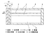
【0005】
図23は、従来の半導体レーザ装置の一例を示す構造図である。レーザチップは、GaAs等の半導体基板1と、活性層2と、活性層2の上方および下方に形成されたクラッド層3と、クラッド層3の上方および下方に形成された電極4などで構成される。
【0006】
半導体レーザ装置は、上述のレーザチップと、レーザ前端面に形成された低反射膜8と、レーザ後端面に形成された高反射膜9などで構成される。
【0007】
一般に、レーザ前端面に用いられる低反射膜8には、真空中でのレーザ発振波長をλとして、λ/4の整数倍±αとなるような光学膜厚を有した単層膜が用いられる。ここで、αは所望の反射率に制御するための修正係数である。
【0008】
半導体レーザの前端面では、レーザ光密度が高くなって、温度が上昇し易い。そのため低反射膜8は、熱拡散板(ヒートスプレッダー)としての役割も果たすように、一般に、膜厚3λ/4±αの酸化アルミニウム膜で形成される。
【0009】
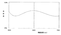
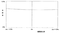
図24は、従来の低反射膜について反射率の波長依存性の一例を示すグラフである。図25は、従来の低反射膜について反射率の膜厚依存性の一例を示すグラフである。ここでは、低反射膜8として、膜厚318.9nm(α=+17nm)の酸化アルミニウム膜(屈折率=1.638)を、発振波長λ=660nmの赤色半導体レーザの前端面に設けている。なお、レーザチップの等価屈折率は3.817である。
【0010】
図25のグラフを見ると、低反射膜8の反射率を6%±1%の範囲に制御したい場合、膜厚設計値da=318.9nmに対して±1%の精度、即ち±3nm程度の精度で低反射膜8の膜厚を制御しなければならないことが判る。このような膜厚精度は、一般に光学薄膜の形成に用いられる蒸着やスパッタでは困難であることから、半導体レーザの製造歩留りの低下を招く。
【0011】
【特許文献1】
特開2001−77456号公報(図1等)
【特許文献2】
特許第3080312号公報(第1図等)
【0012】
【発明が解決しようとする課題】
半導体レーザの低反射膜8を、例えば反射率6±1%の範囲で実現しようとした場合、上記酸化アルミニウム単層膜では膜厚ばらつきを±1%以内に抑えなければならず、反射率制御性が低くなり歩留りが悪化してしまう。
【0013】
本発明の目的は、レーザ端面に形成される反射膜を構成する誘電体膜の膜厚や屈折率が変動しても反射率を安定に制御でき、用途に応じた所望の反射率を容易に実現できる半導体レーザ装置を提供することである。
【0014】
【課題を解決するための手段】
本発明に係る半導体レーザ装置は、レーザチップの光出射面の少なくとも片側に、多層誘電体膜で構成された反射膜を有し、
反射膜は、レーザチップに接する側から順に、屈折率n1の第1誘電体膜、屈折率n2の第2誘電体膜、屈折率n3の第3誘電体膜、屈折率n4の第4誘電体膜を含み、
各屈折率は、n2=n4<n1<n3の関係、またはn2=n4<n3<n1の関係を満たすことを特徴とする。
【0015】
【発明の実施の形態】
実施の形態1.
図1は、本発明の第1実施形態を示す構造図であり、光軸に沿った垂直断面を示している。レーザチップは、GaAs等の半導体基板1と、活性層2と、活性層2の上方および下方に形成されたクラッド層3と、クラッド層3の上方および下方に形成された電極4などで構成される。
【0016】
半導体レーザ装置は、上述のレーザチップと、レーザ前端面に形成された低反射膜10と、レーザ後端面に形成された高反射膜9などで構成される。
【0017】
低反射膜10は、レーザチップに接する側から順に、屈折率n1および膜厚d1の誘電体膜11、屈折率n2および膜厚d2の誘電体膜12、屈折率n3および膜厚d3の誘電体膜13、屈折率n4および膜厚d4の誘電体膜14で形成されている。
【0018】
本実施形態において、誘電体膜12の屈折率n2と誘電体膜14の屈折率n4とが相等しくなるように材料が選定され、さらに誘電体膜11の屈折率n1は屈折率n2(=n4)以上になるように材料が選定され、さらに誘電体膜13の屈折率n3は屈折率n1以上になるように材料が選定される。即ち、各誘電体膜11〜14の屈折率n1〜n4は、n2=n4<n1<n3の関係を満たす。
【0019】
低反射膜10の具体的な構成を例示すると、レーザチップとして発振波長λ=660nmの赤色半導体レーザ(等価屈折率:3.817)を使用した場合、誘電体膜11には屈折率n1=1.638の酸化アルミニウムAl2O3、誘電体膜12および誘電体膜14には屈折率n2=n4=1.489の酸化珪素SiO2、誘電体膜13には屈折率n3=2.063の酸化タンタルTa2O5をそれぞれ使用している。
【0020】
さらに、各誘電体膜11〜14の膜厚d1〜d4は、光学長に換算して発振波長の4分の1、即ちλ/4となるように設定しており、具体的には、誘電体膜11の膜厚d1=100.7nm、誘電体膜12の膜厚d2=110.8nm、誘電体膜13の膜厚d3=80.0nm、誘電体膜14の膜厚d4=110.8nm(=d2)にそれぞれ設定している。
【0021】
こうした構成によって低反射膜10は、発振波長λ=660nmで6%の反射率が得られる。
【0022】
図2は、低反射膜10の反射率について波長依存性を示すグラフである。このグラフから、中心波長λ=660nmで6%の反射率を示しており、図24のグラフと比べて、発振波長の変化に対する反射率変化は格段に小さくなり、レーザ発振波長が変動しても低反射膜10は安定した反射率を示すことが判る。
【0023】
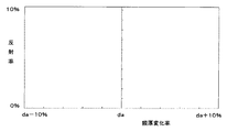
図3は、低反射膜10の反射率について第1誘電体膜11の膜厚依存性を示すグラフである。図4は、低反射膜10の反射率について第2誘電体膜12の膜厚依存性を示すグラフである。図5は、低反射膜10の反射率について第3誘電体膜13の膜厚依存性を示すグラフである。図6は、低反射膜10の反射率について第4誘電体膜14の膜厚依存性を示すグラフである。
【0024】
これらのグラフから、膜厚設計値daで6%の反射率を示しており、図25のグラフと比べて、各誘電体膜の膜厚変化に対する反射率変化は格段に小さくなり、膜厚d1〜d4が膜厚設計値daに対して±10%の範囲で変動しても、低反射膜10の反射率はほとんど変化しておらず、最大でも0.3%の反射率変化に抑制できることが判る。
【0025】
次に、発振波長λ=660nmで7%の反射率を示す低反射膜10を得る場合は、上述と同様に、誘電体膜11には屈折率n1=1.638の酸化アルミニウムAl2O3、誘電体膜12および誘電体膜14には屈折率n2=n4=1.489の酸化珪素SiO2、誘電体膜13には屈折率n3=2.063の酸化タンタルTa2O5をそれぞれ使用し、各誘電体膜の膜厚について、膜厚d1=100.7nm、膜厚d2=d4=100.0nm、膜厚d3=100.0nmにそれぞれ設定している。
【0026】
図7は、低反射膜10の反射率について波長依存性を示すグラフである。このグラフから、中心波長λ=660nmで7%の反射率を示しており、図24のグラフと比べて、発振波長の変化に対する反射率変化は小さくなり、レーザ発振波長が変動しても低反射膜10は安定した反射率を示すことが判る。
【0027】
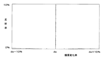
図8は、低反射膜10の反射率について第1誘電体膜11の膜厚依存性を示すグラフである。図9は、低反射膜10の反射率について第2誘電体膜12の膜厚依存性を示すグラフである。図10は、低反射膜10の反射率について第3誘電体膜13の膜厚依存性を示すグラフである。図11は、低反射膜10の反射率について第4誘電体膜14の膜厚依存性を示すグラフである。
【0028】
これらのグラフから、膜厚設計値daで7%の反射率を示しており、図25のグラフと比べて、各誘電体膜の膜厚変化に対する反射率変化は格段に小さくなり、膜厚d1〜d4が膜厚設計値daに対して±10%の範囲で変動しても、低反射膜10の反射率はほとんど変化しておらず、最大でも0.8%の反射率変化に抑制できることが判る。
【0029】
このように各誘電体膜11〜14の屈折率n1〜n4は、n2=n4<n1<n3の関係を満たすことによって、多層誘電体膜の反射率の波長依存性および膜厚依存性が小さくなり、半導体レーザの製造歩留りを向上させることができる。
【0030】
また、屈折率n1は1.6<n1≦1.9の範囲で、屈折率n2は1.3≦n2≦1.6の範囲で、屈折率n3は1.9<n3≦2.3の範囲で、屈折率n4は1.3≦n4≦1.6の範囲であり、膜厚d1は(2・h+1)λ/(4・n1)、膜厚d2は(2・i+1)λ/(4・n2)、膜厚d3は(2・j+1)λ/(4・n3)、膜厚d4は(2・k+1)λ/(4・n4)、(h,i,j,kは0以上の整数)に実質上設定することによって、多層誘電体膜を3〜15%の範囲で所望の反射率に調整することができる。
【0031】
また、各屈折率が、n2=n4<n1<n3という関係を満たすには、誘電体膜11は、Al2O3,CeF3,NdF3,MgO,Y2O3のいずれかで形成し、誘電体膜12および誘電体膜14は、SiO2,MgF2,BaF2,CaF2のいずれかで形成し、誘電体膜13は、Ta2O5,SiO,ZrO2,ZnO,TiO,TiO2,ZnS,Nb2O5,HfO2,AlNのいずれかで形成することが好ましく、これらの材料を使用することによって所望の反射率を有する多層誘電体膜を容易に実現できる。
【0032】
また、誘電体膜11〜14の屈折率n1〜n4は、n2=n4<n1<n3の関係を満たすとともに、膜厚d1〜d4を光学長換算で±30%の範囲で個別に調整することによって、所望の波長において3〜15%の範囲で所望の反射率を実現できる。そのため、用途に応じた仕様変更が容易になり、波長依存性や膜厚依存性を考慮することで半導体レーザ装置の製造歩留りも改善できる。
【0033】
以上の説明では、単一の発振波長を有するレーザ光を発光する半導体レーザ装置について詳述したが、単一のレーザチップ中に互いに異なる発振波長を放射する複数の発光点を有する、いわゆるマルチビームレーザについても上述と同様な低反射膜10を適用することができる。
【0034】
例えば、DVD(デジタルビデオディスク)とCD(コンパクトディスク)の両方の規格に対応可能なレーザチップは、波長660nmのビームと波長780nmのビームを放射する。この場合、2つの波長について所望の反射率を有する多層誘電体膜が望まれる。
【0035】
そこで、各誘電体膜11〜14の各屈折率が、n2=n4<n1<n3という関係を満たすとともに、膜厚d1〜d4を、光学長換算で波長の4分の1を中心膜厚として±30%の範囲で調整することによって、所望の波長ごとに所望の反射率を達成することができ、例えば、図12に示すように、波長660nmおよび波長780nmの両方で約6%の反射率を示す多層誘電体膜を実現することができる。
【0036】
また、上述の半導体レーザ装置を単一のパッケージ内に複数配置し、各レーザチップは互いに異なる発振波長を放射するとともに、各レーザチップの光出射面に設ける多層誘電体膜を同一の材料および同一の膜厚で形成する場合も、マルチビームレーザの場合と同様に、誘電体膜11〜14の膜厚d1〜d4を、光学長換算で波長の4分の1を中心膜厚として±30%の範囲で調整することによって、所望の波長ごとに所望の反射率を達成することができる。
【0037】
実施の形態2.
本実施形態において、半導体レーザ装置の構成は図1のものと同様であるが、低反射膜10は、レーザチップに接する側から順に、屈折率n1および膜厚d1の誘電体膜11、屈折率n2および膜厚d2の誘電体膜12、屈折率n3および膜厚d3の誘電体膜13、屈折率n4および膜厚d4の誘電体膜14で形成し、屈折率n1〜n4は、n2=n4<n3<n1の関係を満たすように材料が選定される。
【0038】
低反射膜10の具体的な構成を例示すると、レーザチップとして発振波長λ=660nmの赤色半導体レーザ(等価屈折率:3.817)を使用した場合、レーザチップに接する誘電体膜11には屈折率n1=2.063の酸化タンタルTa2O5、誘電体膜12および誘電体膜14には屈折率n2=n4=1.489の酸化珪素SiO2、誘電体膜13にはn3=1.638の酸化アルミニウムAl2O3をそれぞれ使用している。
【0039】
さらに、各誘電体膜11〜14の膜厚d1〜d4は、光学長に換算して発振波長の4分の1、即ちλ/4となるように設定しており、具体的には、誘電体膜11の膜厚d1=80.0nm、誘電体膜12の膜厚d2=110.8nm、誘電体膜13の膜厚d3=100.7nm、誘電体膜14の膜厚d4=110.8nm(=d2)にそれぞれ設定している。
【0040】
こうした構成によって低反射膜10は、発振波長λ=660nmで6%の反射率が得られる。
【0041】
図13は、低反射膜10の反射率について波長依存性を示すグラフである。このグラフから、中心波長λ=660nmで6%の反射率を示しており、図24のグラフと比べて、発振波長の変化に対する反射率変化は小さくなり、レーザ発振波長が変動しても低反射膜10は安定した反射率を示すことが判る。
【0042】
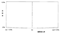
図14は、低反射膜10の反射率について第1誘電体膜11の膜厚依存性を示すグラフである。図15は、低反射膜10の反射率について第2誘電体膜12の膜厚依存性を示すグラフである。図16は、低反射膜10の反射率について第3誘電体膜13の膜厚依存性を示すグラフである。図17は、低反射膜10の反射率について第4誘電体膜14の膜厚依存性を示すグラフである。
【0043】
これらのグラフから、膜厚設計値daで6%の反射率を示しており、図25のグラフと比べて、各誘電体膜の膜厚変化に対する反射率変化は格段に小さくなり、膜厚d1〜d4が膜厚設計値daに対して±10%の範囲で変動しても、低反射膜10の反射率はほとんど変化しておらず、最大でも0.3%の反射率変化に抑制できることが判る。
【0044】
このように各誘電体膜11〜14の屈折率n1〜n4は、n2=n4<n3<n1の関係を満たすことによって、多層誘電体膜の反射率の波長依存性および膜厚依存性が小さくなり、半導体レーザの製造歩留りを向上させることができる。
【0045】
また、屈折率n1は1.9<n1≦2.3の範囲で、屈折率n2は1.3≦n2≦1.6の範囲で、屈折率n3は1.3≦n2≦1.6の範囲で、屈折率n4は1.3≦n4≦1.6の範囲であり、膜厚d1は(2・h+1)λ/(4・n1)、膜厚d2は(2・i+1)λ/(4・n2)、膜厚d3は(2・j+1)λ/(4・n3)、膜厚d4は(2・k+1)λ/(4・n4)、(h,i,j,kは0以上の整数)に実質上設定することによって、多層誘電体膜を3〜15%の範囲で所望の反射率に調整することができる。
【0046】
また、各屈折率が、n2=n4<n3<n1という関係を満たすには、誘電体膜11は、Ta2O5,SiO,ZrO2,ZnO,TiO,TiO2,ZnS,Nb2O5,HfO2,AlNのいずれかで形成し、誘電体膜12および誘電体膜14は、SiO2,MgF2,BaF2,CaF2のいずれかで形成し、誘電体膜13は、Al2O3,CeF3,NdF3,MgO,Y2O3のいずれかで形成することが好ましく、これらの材料を使用することによって所望の反射率を有する多層誘電体膜を容易に実現できる。
【0047】
また、誘電体膜11〜14の屈折率n1〜n4は、n2=n4<n3<n1の関係を満たすとともに、膜厚d1〜d4を光学長換算で±30%の範囲で個別に調整することによって、所望の波長において3〜15%の範囲で所望の反射率を実現できる。そのため、用途に応じた仕様変更が容易になり、波長依存性や膜厚依存性を考慮することで半導体レーザ装置の製造歩留りも改善できる。
【0048】
また、DVD及びCD兼用ピックアップのように、単一のレーザチップ中に互いに異なる発振波長を放射する複数の発光点を有する、いわゆるマルチビームレーザについても上述と同様な低反射膜10を適用することができる。
【0049】
また、上述の半導体レーザ装置を単一のパッケージ内に複数配置し、各レーザチップは互いに異なる発振波長を放射するとともに、各レーザチップの光出射面に設ける多層誘電体膜を同一の材料および同一の膜厚で形成する場合も、マルチビームレーザの場合と同様に、所望の波長ごとに所望の反射率を達成することができる。
【0050】
実施の形態3.
本実施形態において、半導体レーザ装置の構成は図1のものと同様であるが、上述の4層構成の低反射膜10に加えて、発光点以外の領域に第5の誘電体膜と第6の誘電体膜を組み合せた多層誘電体膜を部分的に形成することにより、発光点の領域での反射率より小さい低反射膜を形成している。
【0051】
光ディスク用半導体レーザにおいて、光ディスクのトラッキングにいわゆる所謂3ビーム法が用いられることから、光ディスクからの戻り光が半導体レーザチップの発光点以外の領域に照射されることがある。チップ端面に一様な反射膜を形成した場合、発光点以外の反射率は発光点と同じになるため、光ディスクからの戻り光が更にチップ端面で反射して、再び光ディスクに戻ることにより光ピックアップのトラッキング特性に悪影響を及ぼすことがある。このような悪影響を抑えるために、半導体レーザチップの発光点以外の領域ではできるだけ低反射コーティングがなされていることが望ましい。
【0052】
そこで、レーザチップの光出射面において、上述の4層構成の低反射膜に加えて、発光点以外の領域に第5の誘電体膜と第6の誘電体膜を組み合せた多層誘電体膜を部分的に形成することにより、発光点の領域での反射率より小さい低反射膜を簡単に得ることができる。
【0053】
例えば、4層構成の低反射膜10に接する側から順に、屈折率n5および膜厚d5の誘電体膜Q5、屈折率n6および膜厚d6の誘電体膜Q6、屈折率n7(=n5)および膜厚d7(=d5)の誘電体膜Q7、屈折率n8(=n6)および膜厚d8(=d6)の誘電体膜Q8の2ペア積層膜を形成する場合、膜厚d5〜d8を光学長に換算して1/4発振波長の整数倍に実質上設定することによって、反射率を部分的に小さくできる。
【0054】
例えば、誘電体膜Q5として、屈折率n5=1.640の材料で膜厚d5=100.6nmに、誘電体膜Q6として、屈折率n6=1.450の材料で膜厚d6=113.8nmに、誘電体膜Q7として、屈折率n7=1.640の材料で膜厚d7=100.6nmに、誘電体膜Q8として、屈折率n8=1.450の材料で膜厚d8=113.8nmにそれぞれ形成して、2ペア積層膜をを発光点以外の領域に追加形成した場合、図18に示すように、波長660nmで約0%の反射率を示す無反射膜を実現することができる。
【0055】
図19は、上記無反射膜の反射率について誘電体膜Q5の膜厚依存性を示すグラフである。図20は、上記無反射膜の反射率について誘電体膜Q6の膜厚依存性を示すグラフである。図21は、上記無反射膜の反射率について誘電体膜Q7の膜厚依存性を示すグラフである。図22は、上記無反射膜の反射率について誘電体膜Q8の膜厚依存性を示すグラフである。
【0056】
これらのグラフから、膜厚設計値daで0%の反射率を示しており、各誘電体膜の膜厚変化に対する反射率変化は格段に小さくなり、膜厚d5〜d8が膜厚設計値daに対して±10%の範囲で変動しても、反射率はほとんど変化しておらず、最大でも0.5%の反射率変化に抑制できることが判る。
【0057】
なお上述の各実施形態において、多層誘電体膜をレーザチップの光出射面の片側に設けた例を説明したが、本発明に係る多層誘電体膜をレーザチップの共振器端面の両方に設けても構わない。
【0058】
【発明の効果】
以上詳説したように、多層誘電体膜を構成する第1誘電体膜〜第4誘電体膜の屈折率n1〜n4は、n2=n4<n1<n3の関係、またはn2=n4<n3<n1の関係を満たすことによって、多層誘電体膜の反射率の波長依存性および膜厚依存性が小さくなり、用途に応じた所望の反射率を容易に実現できる。また、そのため半導体レーザの製造歩留りを向上させることができる。
【図面の簡単な説明】
【図1】 本発明の第1実施形態を示す構造図である。
【図2】 低反射膜10の反射率について波長依存性を示すグラフである。
【図3】 低反射膜10の反射率について第1誘電体膜11の膜厚依存性を示すグラフである。
【図4】 低反射膜10の反射率について第2誘電体膜12の膜厚依存性を示すグラフである。
【図5】 低反射膜10の反射率について第3誘電体膜13の膜厚依存性を示すグラフである。
【図6】 低反射膜10の反射率について第4誘電体膜14の膜厚依存性を示すグラフである。
【図7】 低反射膜10の反射率について波長依存性を示すグラフである。
【図8】 低反射膜10の反射率について第1誘電体膜11の膜厚依存性を示すグラフである。
【図9】 低反射膜10の反射率について第2誘電体膜12の膜厚依存性を示すグラフである。
【図10】 低反射膜10の反射率について第3誘電体膜13の膜厚依存性を示すグラフである。
【図11】 低反射膜10の反射率について第4誘電体膜14の膜厚依存性を示すグラフである。
【図12】 2つの波長で約6%の反射率を示す多層誘電体膜の波長依存性を示すグラフである。
【図13】 低反射膜10の反射率について波長依存性を示すグラフである。
【図14】 低反射膜10の反射率について第1誘電体膜11の膜厚依存性を示すグラフである。
【図15】 低反射膜10の反射率について第2誘電体膜12の膜厚依存性を示すグラフである。
【図16】 低反射膜10の反射率について第3誘電体膜13の膜厚依存性を示すグラフである。
【図17】 低反射膜10の反射率について第4誘電体膜14の膜厚依存性を示すグラフである。
【図18】 無反射膜の反射率について波長依存性を示すグラフである。
【図19】 無反射膜の反射率について誘電体膜Q5の膜厚依存性を示すグラフである。
【図20】 無反射膜の反射率について誘電体膜Q6の膜厚依存性を示すグラフである。
【図21】 無反射膜の反射率について誘電体膜Q7の膜厚依存性を示すグラフである。
【図22】 無反射膜の反射率について誘電体膜Q8の膜厚依存性を示すグラフである。
【図23】 従来の半導体レーザ装置の一例を示す構造図である。
【図24】 従来の低反射膜について反射率の波長依存性の一例を示すグラフである。
【図25】 従来の低反射膜について反射率の膜厚依存性の一例を示すグラフである。
【符号の説明】
1 基板、 2 活性層、 3 クラッド層、 4 電極、 9 高反射膜、
10 低反射膜、 11〜14 誘電体膜。[0001]
BACKGROUND OF THE INVENTION
The present invention relates to a semiconductor laser device in which a dielectric reflection film is provided on a light emitting surface.
[0002]
[Prior art]
In a semiconductor laser, a dielectric film is generally formed on the end face of a resonator obtained by cleaving a wafer. By arbitrarily selecting the type, film thickness, and number of layers of the dielectric formed on the end face, it is possible to form a reflectance control film that obtains a desired reflectance. For example, high output can be achieved by lowering the reflectance of the front end face from which the laser light is emitted and increasing the reflectance of the rear end face.
[0003]
However, the reflectance of the front end face does not have to be simply reduced, and it is necessary to select the reflectance according to the application in which the semiconductor laser is used, that is, the required characteristics.
[0004]
For example, in a high-power semiconductor laser, the reflectance at the front end face of the light emission is about 3% to 15%. If an attempt is made to obtain a reflectance of 7%, the controllability of the reflectance is required to be 6% ± 1%. Usually, the reflectance of the front end face from which laser light is emitted in a semiconductor laser is controlled by the thickness and refractive index of a single-layer dielectric film made of Al 2 O 3 , SiO 2 or the like.
[0005]
FIG. 23 is a structural diagram showing an example of a conventional semiconductor laser device. The laser chip includes a semiconductor substrate 1 such as GaAs, an
[0006]
The semiconductor laser device includes the above-described laser chip, a
[0007]
In general, the low-
[0008]
On the front end face of the semiconductor laser, the laser light density increases and the temperature tends to rise. Therefore, the
[0009]
FIG. 24 is a graph showing an example of the wavelength dependence of the reflectance of a conventional low reflection film. FIG. 25 is a graph showing an example of the film thickness dependence of the reflectance for a conventional low reflection film. Here, as the
[0010]
Referring to the graph of FIG. 25, when it is desired to control the reflectivity of the
[0011]
[Patent Document 1]
JP 2001-77456 A (FIG. 1 and the like)
[Patent Document 2]
Japanese Patent No. 3080312 (Fig. 1 etc.)
[0012]
[Problems to be solved by the invention]
When the
[0013]
The object of the present invention is to stably control the reflectance even when the film thickness and refractive index of the dielectric film constituting the reflective film formed on the laser end face vary, and easily achieve a desired reflectance according to the application. A semiconductor laser device that can be realized is provided.
[0014]
[Means for Solving the Problems]
The semiconductor laser device according to the present invention has a reflective film composed of a multilayer dielectric film on at least one side of the light emitting surface of the laser chip,
The reflective films are, in order from the side in contact with the laser chip, a first dielectric film having a refractive index n1, a second dielectric film having a refractive index n2, a third dielectric film having a refractive index n3, and a fourth dielectric having a refractive index n4. Including a membrane,
Each refractive index satisfies a relationship of n2 = n4 <n1 <n3 or a relationship of n2 = n4 <n3 <n1 .
[0015]
DETAILED DESCRIPTION OF THE INVENTION
Embodiment 1 FIG.
FIG. 1 is a structural diagram showing a first embodiment of the present invention, and shows a vertical section along an optical axis. The laser chip includes a semiconductor substrate 1 such as GaAs, an
[0016]
The semiconductor laser device includes the above-described laser chip, a
[0017]
The
[0018]
In this embodiment, the material is selected so that the refractive index n2 of the
[0019]
When a specific configuration of the
[0020]
Furthermore, the film thicknesses d1 to d4 of the
[0021]
With this configuration, the
[0022]
FIG. 2 is a graph showing the wavelength dependence of the reflectance of the low
[0023]
FIG. 3 is a graph showing the film thickness dependence of the
[0024]
From these graphs, the reflectivity of 6% is shown by the film thickness design value da. Compared with the graph of FIG. 25, the change in reflectivity with respect to the change in film thickness of each dielectric film becomes much smaller, and the film thickness d1. Even when ˜d4 fluctuates within a range of ± 10% with respect to the film thickness design value da, the reflectance of the low
[0025]
Next, when obtaining the
[0026]
FIG. 7 is a graph showing the wavelength dependence of the reflectance of the low
[0027]
FIG. 8 is a graph showing the film thickness dependence of the
[0028]
From these graphs, the reflectivity of 7% is shown by the film thickness design value da. Compared with the graph of FIG. 25, the change in reflectivity with respect to the change in film thickness of each dielectric film becomes much smaller, and the film thickness d1. Even if ˜d4 fluctuates in the range of ± 10% with respect to the film thickness design value da, the reflectance of the low
[0029]
As described above, the refractive indexes n1 to n4 of the
[0030]
The refractive index n1 is in the range of 1.6 <n1 ≦ 1.9 , the refractive index n2 is in the range of 1.3 ≦ n2 ≦ 1.6 , and the refractive index n3 is 1.9 <n3 ≦ 2.3 . The refractive index n4 is in the range of 1.3 ≦ n4 ≦ 1.6 , the film thickness d1 is (2 · h + 1) λ / (4 · n1), and the film thickness d2 is (2 · i + 1) λ / ( 4 · n2), film thickness d3 is (2 · j + 1) λ / (4 · n3), film thickness d4 is (2 · k + 1) λ / (4 · n4), and (h, i, j, k is 0 or more) The multilayer dielectric film can be adjusted to a desired reflectance within a range of 3 to 15%.
[0031]
In addition, in order for each refractive index to satisfy the relationship of n2 = n4 <n1 <n3 , the
[0032]
The refractive indexes n1 to n4 of the
[0033]
In the above description, the semiconductor laser device that emits laser light having a single oscillation wavelength has been described in detail. However, a so-called multi-beam having a plurality of emission points that emit different oscillation wavelengths in a single laser chip. The
[0034]
For example, a laser chip capable of supporting both DVD (digital video disc) and CD (compact disc) standards emits a beam with a wavelength of 660 nm and a beam with a wavelength of 780 nm. In this case, a multilayer dielectric film having desired reflectivities for two wavelengths is desired.
[0035]
Therefore, the refractive indexes of the
[0036]
Further, a plurality of the semiconductor laser devices described above are arranged in a single package, each laser chip emits a different oscillation wavelength, and the multilayer dielectric film provided on the light emitting surface of each laser chip is made of the same material and the same In the same way as in the case of the multi-beam laser, the film thicknesses d1 to d4 of the
[0037]
In this embodiment, the configuration of the semiconductor laser device is the same as that shown in FIG. 1, but the
[0038]
When a specific configuration of the
[0039]
Furthermore, the film thicknesses d1 to d4 of the
[0040]
With this configuration, the
[0041]
FIG. 13 is a graph showing the wavelength dependence of the reflectance of the low
[0042]
FIG. 14 is a graph showing the film thickness dependence of the
[0043]
From these graphs, the reflectivity of 6% is shown by the film thickness design value da. Compared with the graph of FIG. 25, the change in reflectivity with respect to the change in film thickness of each dielectric film becomes much smaller, and the film thickness d1. Even when ˜d4 fluctuates within a range of ± 10% with respect to the film thickness design value da, the reflectance of the low
[0044]
As described above, the refractive indexes n1 to n4 of the
[0045]
The refractive index n1 is in the range of 1.9 <n1 ≦ 2.3 , the refractive index n2 is in the range of 1.3 ≦ n2 ≦ 1.6 , and the refractive index n3 is in the range of 1.3 ≦ n2 ≦ 1.6 . The refractive index n4 is in the range of 1.3 ≦ n4 ≦ 1.6 , the film thickness d1 is (2 · h + 1) λ / (4 · n1), and the film thickness d2 is (2 · i + 1) λ / ( 4 · n2), film thickness d3 is (2 · j + 1) λ / (4 · n3), film thickness d4 is (2 · k + 1) λ / (4 · n4), and (h, i, j, k is 0 or more) The multilayer dielectric film can be adjusted to a desired reflectance within a range of 3 to 15%.
[0046]
In order for each refractive index to satisfy the relationship of n2 = n4 <n3 <n1 , the
[0047]
The refractive indexes n1 to n4 of the
[0048]
The
[0049]
Further, a plurality of the semiconductor laser devices described above are arranged in a single package, each laser chip emits a different oscillation wavelength, and the multilayer dielectric film provided on the light emitting surface of each laser chip is made of the same material and the same Also in the case of forming with a film thickness of, it is possible to achieve a desired reflectance for each desired wavelength, as in the case of a multi-beam laser.
[0050]
In this embodiment, the configuration of the semiconductor laser device is the same as that shown in FIG. 1, but in addition to the above-described four-layer low-
[0051]
Since a so-called three-beam method is used for tracking an optical disk in a semiconductor laser for an optical disk, the return light from the optical disk may be irradiated onto a region other than the light emitting point of the semiconductor laser chip. When a uniform reflection film is formed on the chip end surface, the reflectance other than the light emitting point is the same as that of the light emitting point. Therefore, the return light from the optical disk is further reflected by the chip end surface and returned to the optical disk again. May adversely affect the tracking characteristics. In order to suppress such an adverse effect, it is desirable that a low-reflection coating is provided as much as possible in a region other than the light emitting point of the semiconductor laser chip.
[0052]
Therefore, on the light emitting surface of the laser chip, in addition to the above-described four-layer low-reflection film, a multilayer dielectric film in which a fifth dielectric film and a sixth dielectric film are combined in a region other than the light emitting point. By forming it partially, a low reflection film smaller than the reflectance in the region of the light emitting point can be easily obtained.
[0053]
For example, a dielectric film Q5 having a refractive index n5 and a film thickness d5, a dielectric film Q6 having a refractive index n6 and a film thickness d6, a refractive index n7 (= n5) When forming a two-pair laminated film of a dielectric film Q7 having a film thickness d7 (= d5) and a dielectric film Q8 having a refractive index n8 (= n6) and a film thickness d8 (= d6), the film thicknesses d5 to d8 are optical. The reflectance can be partially reduced by converting the length into an integral multiple of the quarter oscillation wavelength.
[0054]
For example, the dielectric film Q5 is made of a material having a refractive index n5 = 1.640, and the film thickness is d5 = 100.6 nm. The dielectric film Q6 is made of a material having a refractive index n6 = 1.450, and the film thickness is d6 = 13.8 nm. Further, as the dielectric film Q7, the film thickness d7 = 10.66 nm with a material having a refractive index n7 = 1.640, and as the dielectric film Q8, the film thickness d8 = 13.8 nm with a material having a refractive index n8 = 1.450. When a two-pair laminated film is additionally formed in a region other than the light emitting point, a non-reflective film exhibiting a reflectance of about 0% at a wavelength of 660 nm can be realized as shown in FIG. .
[0055]
FIG. 19 is a graph showing the film thickness dependence of the dielectric film Q5 with respect to the reflectance of the non-reflective film. FIG. 20 is a graph showing the film thickness dependence of the dielectric film Q6 with respect to the reflectance of the non-reflective film. FIG. 21 is a graph showing the film thickness dependence of the dielectric film Q7 with respect to the reflectance of the non-reflective film. FIG. 22 is a graph showing the film thickness dependence of the dielectric film Q8 with respect to the reflectance of the non-reflective film.
[0056]
From these graphs, the reflectivity of 0% is shown by the film thickness design value da, the change in reflectivity with respect to the film thickness change of each dielectric film is remarkably small, and the film thickness d5 to d8 is the film thickness design value da. However, even if it fluctuates within a range of ± 10%, the reflectance hardly changes, and it can be seen that the reflectance change can be suppressed to 0.5% at the maximum.
[0057]
In each of the above-described embodiments, the example in which the multilayer dielectric film is provided on one side of the light emitting surface of the laser chip has been described. However, the multilayer dielectric film according to the present invention is provided on both the resonator end faces of the laser chip. It doesn't matter.
[0058]
【The invention's effect】
As described in detail above, the refractive indexes n1 to n4 of the first dielectric film to the fourth dielectric film constituting the multilayer dielectric film are as follows: n2 = n4 <n1 <n3 , or n2 = n4 <n3 <n1 By satisfying this relationship, the wavelength dependency and film thickness dependency of the reflectance of the multilayer dielectric film are reduced, and a desired reflectance according to the application can be easily realized. Therefore, the manufacturing yield of the semiconductor laser can be improved.
[Brief description of the drawings]
FIG. 1 is a structural diagram showing a first embodiment of the present invention.
FIG. 2 is a graph showing the wavelength dependence of the reflectance of the low
FIG. 3 is a graph showing the film thickness dependence of the
4 is a graph showing the film thickness dependence of the
FIG. 5 is a graph showing the film thickness dependence of the
FIG. 6 is a graph showing the film thickness dependence of the fourth dielectric film with respect to the reflectance of the low reflective film.
7 is a graph showing the wavelength dependence of the reflectance of the low
FIG. 8 is a graph showing the film thickness dependence of the
9 is a graph showing the film thickness dependence of the
10 is a graph showing the film thickness dependence of the
11 is a graph showing the film thickness dependence of the
FIG. 12 is a graph showing the wavelength dependence of a multilayer dielectric film showing a reflectivity of about 6% at two wavelengths.
13 is a graph showing the wavelength dependence of the reflectance of the low
14 is a graph showing the film thickness dependence of the
15 is a graph showing the film thickness dependence of the
16 is a graph showing the film thickness dependence of the
17 is a graph showing the film thickness dependence of the
FIG. 18 is a graph showing the wavelength dependence of the reflectance of an antireflective film.
FIG. 19 is a graph showing the film thickness dependence of the dielectric film Q5 with respect to the reflectance of the non-reflective film.
FIG. 20 is a graph showing the film thickness dependence of the dielectric film Q6 with respect to the reflectance of the non-reflective film.
FIG. 21 is a graph showing the film thickness dependence of the dielectric film Q7 with respect to the reflectance of the non-reflective film.
FIG. 22 is a graph showing the film thickness dependence of the dielectric film Q8 with respect to the reflectance of the non-reflective film.
FIG. 23 is a structural diagram showing an example of a conventional semiconductor laser device.
FIG. 24 is a graph showing an example of wavelength dependence of reflectance for a conventional low reflection film.
FIG. 25 is a graph showing an example of film thickness dependence of reflectance for a conventional low reflection film.
[Explanation of symbols]
1 substrate, 2 active layer, 3 cladding layer, 4 electrode, 9 highly reflective film,
10 Low reflection film, 11-14 Dielectric film.
Claims (12)
反射膜は、レーザチップに接する側から順に、屈折率n1の第1誘電体膜、屈折率n2の第2誘電体膜、屈折率n3の第3誘電体膜、屈折率n4の第4誘電体膜を含み、
各屈折率は、n2=n4<n1<n3の関係を満たすことを特徴とする半導体レーザ装置。In a semiconductor laser device having a reflective film composed of a multilayer dielectric film on at least one side of a light emitting surface of a laser chip,
The reflective films are, in order from the side in contact with the laser chip, a first dielectric film having a refractive index n1, a second dielectric film having a refractive index n2, a third dielectric film having a refractive index n3, and a fourth dielectric having a refractive index n4. Including a membrane,
Each refractive index satisfies the relationship of n2 = n4 <n1 <n3.
反射膜は、レーザチップに接する側から順に、屈折率n1の第1誘電体膜、屈折率n2の第2誘電体膜、屈折率n3の第3誘電体膜、屈折率n4の第4誘電体膜を含み、
各屈折率は、n2=n4<n3<n1の関係を満たすことを特徴とする半導体レーザ装置。In a semiconductor laser device having a reflective film composed of a multilayer dielectric film on at least one side of a light emitting surface of a laser chip,
The reflective films are, in order from the side in contact with the laser chip, a first dielectric film having a refractive index n1, a second dielectric film having a refractive index n2, a third dielectric film having a refractive index n3, and a fourth dielectric having a refractive index n4. Including a membrane,
Each refractive index satisfies the relationship of n2 = n4 <n3 <n1.
反射膜は、3〜15%の反射率を有し、レーザチップに接する側から順に、屈折率n1および膜厚d1の第1誘電体膜、屈折率n2および膜厚d2の第2誘電体膜、屈折率n3および膜厚d3の第3誘電体膜、屈折率n4および膜厚d4の第4誘電体膜を含み、
屈折率n1は1.6<n1≦1.9の範囲で、屈折率n2は1.3≦n2≦1.6の範囲で、屈折率n3は1.9<n3≦2.3の範囲で、屈折率n4は1.3≦n4≦1.6の範囲であり、
膜厚d1は(2・h+1)λ/(4・n1)、膜厚d2は(2・i+1)λ/(4・n2)、膜厚d3は(2・j+1)λ/(4・n3)、膜厚d4は(2・k+1)λ/(4・n4)、(h,i,j,kは0以上の整数)に実質上設定されていることを特徴とする半導体レーザ装置。In a semiconductor laser device having a reflective film composed of a multilayer dielectric film on at least one side of a light emitting surface of a laser chip and emitting light having an oscillation wavelength λ,
The reflective film has a reflectivity of 3 to 15%, and in order from the side in contact with the laser chip, a first dielectric film having a refractive index n1 and a film thickness d1, and a second dielectric film having a refractive index n2 and a film thickness d2 , A third dielectric film having a refractive index n3 and a film thickness d3, a fourth dielectric film having a refractive index n4 and a film thickness d4,
The refractive index n1 is in the range of 1.6 <n1 ≦ 1.9, the refractive index n2 is in the range of 1.3 ≦ n2 ≦ 1.6, and the refractive index n3 is in the range of 1.9 <n3 ≦ 2.3. The refractive index n4 is in the range of 1.3 ≦ n4 ≦ 1.6,
The film thickness d1 is (2 · h + 1) λ / (4 · n1), the film thickness d2 is (2 · i + 1) λ / (4 · n2), and the film thickness d3 is (2 · j + 1) λ / (4 · n3). The semiconductor laser device is characterized in that the film thickness d4 is substantially set to (2 · k + 1) λ / (4 · n4) and (h, i, j, k are integers of 0 or more).
反射膜は、3〜15%の反射率を有し、レーザチップに接する側から順に、屈折率n1および膜厚d1の第1誘電体膜、屈折率n2および膜厚d2の第2誘電体膜、屈折率n3および膜厚d3の第3誘電体膜、屈折率n4および膜厚d4の第4誘電体膜を含み、
屈折率n1は1.9<n1≦2.3の範囲で、屈折率n2は1.3≦n2≦1.6の範囲で、屈折率n3は1.6<n3≦1.9の範囲で、屈折率n4は1.3≦n4≦1.6の範囲であり、
膜厚d1は(2・h+1)λ/(4・n1)、膜厚d2は(2・i+1)λ/(4・n2)、膜厚d3は(2・j+1)λ/(4・n3)、膜厚d4は(2・k+1)λ/(4・n4)、(h,i,j,kは0以上の整数)に実質上設定されていることを特徴とする半導体レーザ装置。In a semiconductor laser device having a reflective film composed of a multilayer dielectric film on at least one side of a light emitting surface of a laser chip and emitting light having an oscillation wavelength λ,
The reflective film has a reflectivity of 3 to 15%, and in order from the side in contact with the laser chip, a first dielectric film having a refractive index n1 and a film thickness d1, and a second dielectric film having a refractive index n2 and a film thickness d2 , A third dielectric film having a refractive index n3 and a film thickness d3, a fourth dielectric film having a refractive index n4 and a film thickness d4,
The refractive index n1 is in the range of 1.9 <n1 ≦ 2.3, the refractive index n2 is in the range of 1.3 ≦ n2 ≦ 1.6, and the refractive index n3 is in the range of 1.6 <n3 ≦ 1.9. The refractive index n4 is in the range of 1.3 ≦ n4 ≦ 1.6,
The film thickness d1 is (2 · h + 1) λ / (4 · n1), the film thickness d2 is (2 · i + 1) λ / (4 · n2), and the film thickness d3 is (2 · j + 1) λ / (4 · n3). The semiconductor laser device is characterized in that the film thickness d4 is substantially set to (2 · k + 1) λ / (4 · n4) and (h, i, j, k are integers of 0 or more).
第2誘電体膜および第4誘電体膜は、SiO2,MgF2,BaF2,CaF2のいずれかで形成され、
第3誘電体膜は、Ta2O5,SiO,ZrO2,ZnO,TiO,TiO2,ZnS,Nb2O5,HfO2,AlNのいずれかで形成されることを特徴とする請求項1または4記載の半導体レーザ装置。The first dielectric film is formed of any one of Al 2 O 3 , CeF 3 , NdF 3 , MgO, and Y 2 O 3 .
The second dielectric film and the fourth dielectric film are formed of any one of SiO 2 , MgF 2 , BaF 2 , and CaF 2 ,
2. The third dielectric film is formed of any one of Ta 2 O 5 , SiO, ZrO 2 , ZnO, TiO, TiO 2 , ZnS, Nb 2 O 5 , HfO 2 , and AlN. Or the semiconductor laser device according to 4;
第2誘電体膜および第4誘電体膜は、SiO2,MgF2,BaF2,CaF2のいずれかで形成され、
第3誘電体膜は、Al2O3,CeF3,NdF3,MgO,Y2O3のいずれかで形成されることを特徴とする請求項2または5記載の半導体レーザ装置。The first dielectric film is formed of any of Ta 2 O 5 , SiO, ZrO 2 , ZnO, TiO, TiO 2 , ZnS, Nb 2 O 5 , HfO 2 , and AlN.
The second dielectric film and the fourth dielectric film are formed of any one of SiO 2 , MgF 2 , BaF 2 , and CaF 2 ,
6. The semiconductor laser device according to claim 2, wherein the third dielectric film is formed of any one of Al 2 O 3 , CeF 3 , NdF 3 , MgO, and Y 2 O 3 .
第6誘電体膜は、SiO2,MgF2,BaF2,CaF2のいずれかで形成されることを特徴とする請求項9記載の半導体レーザ装置。The fifth dielectric film is formed of any one of Al 2 O 3 , CeF 3 , NdF 3 , MgO, Y 2 O 3 ,
The sixth dielectric layer, a semiconductor laser device according to claim 9, characterized in that it is formed in one of SiO 2, MgF 2, BaF 2 , CaF 2.
各レーザチップは、互いに異なる発振波長を放射し、
各レーザチップの光出射面に設けられた多層誘電体膜は、同一の材料および同一の膜厚で形成されていることを特徴とする半導体レーザ装置。A plurality of semiconductor laser devices according to claim 1 are arranged in a single package,
Each laser chip emits a different oscillation wavelength,
A semiconductor laser device characterized in that the multilayer dielectric film provided on the light emitting surface of each laser chip is formed of the same material and the same film thickness.
Priority Applications (8)
| Application Number | Priority Date | Filing Date | Title |
|---|---|---|---|
| JP2003088905A JP4097552B2 (en) | 2003-03-27 | 2003-03-27 | Semiconductor laser device |
| TW093105080A TWI239703B (en) | 2003-03-27 | 2004-02-27 | Semiconductor laser device |
| US10/791,889 US7106775B2 (en) | 2003-03-27 | 2004-03-04 | Semiconductor laser devices |
| DE102004013109A DE102004013109B4 (en) | 2003-03-27 | 2004-03-17 | Semiconductor laser device |
| KR1020040020390A KR100668096B1 (en) | 2003-03-27 | 2004-03-25 | Semiconductor laser device |
| CNB2004100313021A CN1303732C (en) | 2003-03-27 | 2004-03-26 | Semiconductor laser devices |
| CNB2006100550793A CN100411262C (en) | 2003-03-27 | 2004-03-26 | Semiconductor laser devices |
| KR1020060086769A KR100709281B1 (en) | 2003-03-27 | 2006-09-08 | Semiconductor laser device |
Applications Claiming Priority (1)
| Application Number | Priority Date | Filing Date | Title |
|---|---|---|---|
| JP2003088905A JP4097552B2 (en) | 2003-03-27 | 2003-03-27 | Semiconductor laser device |
Publications (3)
| Publication Number | Publication Date |
|---|---|
| JP2004296903A JP2004296903A (en) | 2004-10-21 |
| JP2004296903A5 JP2004296903A5 (en) | 2005-11-04 |
| JP4097552B2 true JP4097552B2 (en) | 2008-06-11 |
Family
ID=32985224
Family Applications (1)
| Application Number | Title | Priority Date | Filing Date |
|---|---|---|---|
| JP2003088905A Expired - Lifetime JP4097552B2 (en) | 2003-03-27 | 2003-03-27 | Semiconductor laser device |
Country Status (6)
| Country | Link |
|---|---|
| US (1) | US7106775B2 (en) |
| JP (1) | JP4097552B2 (en) |
| KR (2) | KR100668096B1 (en) |
| CN (2) | CN100411262C (en) |
| DE (1) | DE102004013109B4 (en) |
| TW (1) | TWI239703B (en) |
Cited By (1)
| Publication number | Priority date | Publication date | Assignee | Title |
|---|---|---|---|---|
| JPH0839698A (en) * | 1994-07-27 | 1996-02-13 | Mitsui Petrochem Ind Ltd | Coupling of sprinkling tube |
Families Citing this family (24)
| Publication number | Priority date | Publication date | Assignee | Title |
|---|---|---|---|---|
| JP2003243764A (en) * | 2002-02-19 | 2003-08-29 | Matsushita Electric Ind Co Ltd | Semiconductor laser and its manufacturing method |
| JP2004327581A (en) * | 2003-04-23 | 2004-11-18 | Mitsubishi Electric Corp | Semiconductor laser equipment |
| JP2004327678A (en) * | 2003-04-24 | 2004-11-18 | Sony Corp | Multiwavelength semiconductor laser and its manufacturing method |
| JP4286683B2 (en) * | 2004-02-27 | 2009-07-01 | ローム株式会社 | Semiconductor laser |
| JP2006128475A (en) * | 2004-10-29 | 2006-05-18 | Mitsubishi Electric Corp | Semiconductor laser |
| JP2006351966A (en) * | 2005-06-17 | 2006-12-28 | Sony Corp | Multi-wavelength semiconductor laser device |
| JP4923489B2 (en) | 2005-09-05 | 2012-04-25 | 三菱電機株式会社 | Semiconductor laser device |
| KR100853241B1 (en) * | 2005-12-16 | 2008-08-20 | 샤프 가부시키가이샤 | Nitride Semiconductor Light Emitting Device and Method of Fabricating Nitride Semiconductor Laser Device |
| JP5191650B2 (en) * | 2005-12-16 | 2013-05-08 | シャープ株式会社 | Nitride semiconductor light emitting device and method for manufacturing nitride semiconductor light emitting device |
| JP5004597B2 (en) | 2006-03-06 | 2012-08-22 | シャープ株式会社 | Nitride semiconductor light emitting device and method for manufacturing nitride semiconductor light emitting device |
| JP5430826B2 (en) | 2006-03-08 | 2014-03-05 | シャープ株式会社 | Nitride semiconductor laser device |
| JP2007280975A (en) * | 2006-03-13 | 2007-10-25 | Mitsubishi Electric Corp | Semiconductor laser |
| JP4444304B2 (en) * | 2006-04-24 | 2010-03-31 | シャープ株式会社 | Nitride semiconductor light emitting device and method for manufacturing nitride semiconductor light emitting device |
| JP4294699B2 (en) | 2007-02-26 | 2009-07-15 | 三菱電機株式会社 | Semiconductor laser device |
| JP5162926B2 (en) | 2007-03-07 | 2013-03-13 | 三菱電機株式会社 | Manufacturing method of semiconductor laser device |
| JP4946524B2 (en) | 2007-03-08 | 2012-06-06 | 三菱電機株式会社 | Semiconductor laser device |
| JP2009170801A (en) * | 2008-01-18 | 2009-07-30 | Mitsubishi Electric Corp | Semiconductor laser |
| JP5443356B2 (en) * | 2008-07-10 | 2014-03-19 | 株式会社東芝 | Semiconductor laser device |
| JP2010219436A (en) * | 2009-03-18 | 2010-09-30 | Sony Corp | Multi-wavelength semiconductor laser and optical recording and reproducing device |
| CN106207753B (en) * | 2016-09-06 | 2019-09-03 | 青岛海信宽带多媒体技术有限公司 | Semiconductor laser chip and its manufacturing method, semicondcutor laser unit |
| DE102017112610A1 (en) * | 2017-06-08 | 2018-12-13 | Osram Opto Semiconductors Gmbh | Edge-emitting semiconductor laser and operating method for such a semiconductor laser |
| CN111193184A (en) * | 2019-12-30 | 2020-05-22 | 腾景科技股份有限公司 | Ultra-narrow band ultra-thin reflecting film plated on cavity surface of semiconductor laser and used for mode selection |
| KR102397558B1 (en) * | 2020-10-29 | 2022-05-17 | 주식회사 오이솔루션 | Distributed feedback semiconductor laser |
| CN113402275B (en) * | 2021-08-12 | 2022-09-02 | 齐鲁工业大学 | Multilayer BMN dielectric thin film material and preparation method thereof |
Family Cites Families (18)
| Publication number | Priority date | Publication date | Assignee | Title |
|---|---|---|---|---|
| DE3728305A1 (en) * | 1987-08-25 | 1989-03-09 | Standard Elektrik Lorenz Ag | SEMICONDUCTOR LASER WITH CONSTANT DIFFERENTIAL QUANTUM EXCHANGER OR CONSTANT OPTICAL OUTPUT |
| JPH0642582B2 (en) | 1988-06-27 | 1994-06-01 | シャープ株式会社 | Dielectric multilayer coating film |
| US4925259A (en) | 1988-10-20 | 1990-05-15 | The United States Of America As Represented By The United States Department Of Energy | Multilayer optical dielectric coating |
| JP3080312B2 (en) | 1989-10-31 | 2000-08-28 | ソニー株式会社 | Manufacturing method of semiconductor laser |
| JPH0418784A (en) | 1990-02-13 | 1992-01-22 | Fuji Electric Co Ltd | Protective film for semiconductor laser element |
| JP3014208B2 (en) * | 1992-02-27 | 2000-02-28 | 三菱電機株式会社 | Semiconductor optical device |
| JP3399049B2 (en) | 1992-10-27 | 2003-04-21 | 松下電器産業株式会社 | Semiconductor laser device |
| JPH06138303A (en) * | 1992-10-28 | 1994-05-20 | Olympus Optical Co Ltd | Antireflection film of plastic optical parts |
| JP3863577B2 (en) * | 1994-11-14 | 2006-12-27 | 三洋電機株式会社 | Semiconductor laser |
| JP3470476B2 (en) * | 1995-11-02 | 2003-11-25 | ソニー株式会社 | Semiconductor light emitting device |
| JP3538515B2 (en) | 1997-03-04 | 2004-06-14 | シャープ株式会社 | Semiconductor laser device |
| US6020992A (en) | 1997-06-16 | 2000-02-01 | Laser Power Corporation | Low absorption coatings for infrared laser optical elements |
| US6094730A (en) * | 1997-10-27 | 2000-07-25 | Hewlett-Packard Company | Hardware-assisted firmware tracing method and apparatus |
| JP4613374B2 (en) | 1999-09-07 | 2011-01-19 | ソニー株式会社 | Semiconductor laser |
| JP2001257413A (en) * | 2000-03-14 | 2001-09-21 | Toshiba Electronic Engineering Corp | Semiconductor laser device and its manufacturing method |
| JP4033644B2 (en) | 2000-07-18 | 2008-01-16 | 日亜化学工業株式会社 | Gallium nitride light emitting device |
| JP2002094173A (en) * | 2000-09-14 | 2002-03-29 | Mitsubishi Electric Corp | Semiconductor laser device |
| JP2002223030A (en) | 2001-01-24 | 2002-08-09 | Toshiba Corp | Semiconductor laser device |
-
2003
- 2003-03-27 JP JP2003088905A patent/JP4097552B2/en not_active Expired - Lifetime
-
2004
- 2004-02-27 TW TW093105080A patent/TWI239703B/en active
- 2004-03-04 US US10/791,889 patent/US7106775B2/en active Active
- 2004-03-17 DE DE102004013109A patent/DE102004013109B4/en not_active Expired - Lifetime
- 2004-03-25 KR KR1020040020390A patent/KR100668096B1/en active IP Right Grant
- 2004-03-26 CN CNB2006100550793A patent/CN100411262C/en not_active Expired - Lifetime
- 2004-03-26 CN CNB2004100313021A patent/CN1303732C/en not_active Expired - Lifetime
-
2006
- 2006-09-08 KR KR1020060086769A patent/KR100709281B1/en active IP Right Grant
Cited By (1)
| Publication number | Priority date | Publication date | Assignee | Title |
|---|---|---|---|---|
| JPH0839698A (en) * | 1994-07-27 | 1996-02-13 | Mitsui Petrochem Ind Ltd | Coupling of sprinkling tube |
Also Published As
| Publication number | Publication date |
|---|---|
| CN1303732C (en) | 2007-03-07 |
| DE102004013109B4 (en) | 2010-02-04 |
| TWI239703B (en) | 2005-09-11 |
| JP2004296903A (en) | 2004-10-21 |
| KR100668096B1 (en) | 2007-01-15 |
| TW200423505A (en) | 2004-11-01 |
| KR20060102321A (en) | 2006-09-27 |
| DE102004013109A1 (en) | 2004-11-11 |
| US20040190576A1 (en) | 2004-09-30 |
| CN1819378A (en) | 2006-08-16 |
| US7106775B2 (en) | 2006-09-12 |
| CN100411262C (en) | 2008-08-13 |
| KR20040084838A (en) | 2004-10-06 |
| CN1543026A (en) | 2004-11-03 |
| KR100709281B1 (en) | 2007-04-19 |
Similar Documents
| Publication | Publication Date | Title |
|---|---|---|
| JP4097552B2 (en) | Semiconductor laser device | |
| US20060239321A1 (en) | Semiconductor laser device | |
| JP2004327581A (en) | Semiconductor laser equipment | |
| US6487227B1 (en) | Semiconductor laser | |
| JP2004327678A (en) | Multiwavelength semiconductor laser and its manufacturing method | |
| JP3635880B2 (en) | Surface emitting semiconductor laser and manufacturing method thereof | |
| US20100238784A1 (en) | Multiwavelength semiconductor laser and optical recording/reproducing device | |
| KR100598651B1 (en) | Semiconductor laser device | |
| JP2008294090A (en) | Semiconductor laser device | |
| JP4294699B2 (en) | Semiconductor laser device | |
| KR100528857B1 (en) | Semiconductor optical device and semiconductor laser module using the semiconductor optical device | |
| JP2003101126A (en) | Semiconductor laser device and method of manufacturing the same | |
| US20040047383A1 (en) | Semiconductor optical device and semiconductor laser module using the semiconductor optical device | |
| JP2006303041A (en) | Semiconductor laser device | |
| JP4613374B2 (en) | Semiconductor laser | |
| US20240146035A1 (en) | Semiconductor laser device | |
| JP2006165478A (en) | Semiconductor laser | |
| JPH06224514A (en) | End surface coating for semiconductor laser | |
| JP2010171182A (en) | Multiwavelength semiconductor laser device | |
| JP2020031239A5 (en) | ||
| JP2008172088A (en) | Semiconductor laser device | |
| JP2008016799A (en) | Semiconductor laser device | |
| JP2003031899A (en) | Laser diode using reflecting film including air layer and its manufacturing method | |
| JPH08148764A (en) | Semiconductor laser element | |
| KR20050020502A (en) | Method of depositing reflection layer of semiconductor laser diode |
Legal Events
| Date | Code | Title | Description |
|---|---|---|---|
| A621 | Written request for application examination |
Free format text: JAPANESE INTERMEDIATE CODE: A621 Effective date: 20041027 |
|
| A521 | Request for written amendment filed |
Free format text: JAPANESE INTERMEDIATE CODE: A523 Effective date: 20050817 |
|
| A977 | Report on retrieval |
Free format text: JAPANESE INTERMEDIATE CODE: A971007 Effective date: 20070905 |
|
| A131 | Notification of reasons for refusal |
Free format text: JAPANESE INTERMEDIATE CODE: A131 Effective date: 20070918 |
|
| A521 | Request for written amendment filed |
Free format text: JAPANESE INTERMEDIATE CODE: A523 Effective date: 20071115 |
|
| A521 | Request for written amendment filed |
Free format text: JAPANESE INTERMEDIATE CODE: A821 Effective date: 20071115 |
|
| TRDD | Decision of grant or rejection written | ||
| A01 | Written decision to grant a patent or to grant a registration (utility model) |
Free format text: JAPANESE INTERMEDIATE CODE: A01 Effective date: 20080304 |
|
| A61 | First payment of annual fees (during grant procedure) |
Free format text: JAPANESE INTERMEDIATE CODE: A61 Effective date: 20080311 |
|
| R150 | Certificate of patent or registration of utility model |
Ref document number: 4097552 Country of ref document: JP Free format text: JAPANESE INTERMEDIATE CODE: R150 Free format text: JAPANESE INTERMEDIATE CODE: R150 |
|
| FPAY | Renewal fee payment (event date is renewal date of database) |
Free format text: PAYMENT UNTIL: 20110321 Year of fee payment: 3 |
|
| FPAY | Renewal fee payment (event date is renewal date of database) |
Free format text: PAYMENT UNTIL: 20110321 Year of fee payment: 3 |
|
| FPAY | Renewal fee payment (event date is renewal date of database) |
Free format text: PAYMENT UNTIL: 20120321 Year of fee payment: 4 |
|
| FPAY | Renewal fee payment (event date is renewal date of database) |
Free format text: PAYMENT UNTIL: 20130321 Year of fee payment: 5 |
|
| FPAY | Renewal fee payment (event date is renewal date of database) |
Free format text: PAYMENT UNTIL: 20130321 Year of fee payment: 5 |
|
| FPAY | Renewal fee payment (event date is renewal date of database) |
Free format text: PAYMENT UNTIL: 20140321 Year of fee payment: 6 |
|
| R250 | Receipt of annual fees |
Free format text: JAPANESE INTERMEDIATE CODE: R250 |
|
| R250 | Receipt of annual fees |
Free format text: JAPANESE INTERMEDIATE CODE: R250 |
|
| R250 | Receipt of annual fees |
Free format text: JAPANESE INTERMEDIATE CODE: R250 |
|
| R250 | Receipt of annual fees |
Free format text: JAPANESE INTERMEDIATE CODE: R250 |
|
| R250 | Receipt of annual fees |
Free format text: JAPANESE INTERMEDIATE CODE: R250 |
|
| R250 | Receipt of annual fees |
Free format text: JAPANESE INTERMEDIATE CODE: R250 |
|
| R250 | Receipt of annual fees |
Free format text: JAPANESE INTERMEDIATE CODE: R250 |
|
| R250 | Receipt of annual fees |
Free format text: JAPANESE INTERMEDIATE CODE: R250 |
|
| EXPY | Cancellation because of completion of term |