JP2010146683A - Method of forming protective film, protective film obtained by the method and magnetic recording medium including the protective film - Google Patents
Method of forming protective film, protective film obtained by the method and magnetic recording medium including the protective film Download PDFInfo
- Publication number
- JP2010146683A JP2010146683A JP2008325922A JP2008325922A JP2010146683A JP 2010146683 A JP2010146683 A JP 2010146683A JP 2008325922 A JP2008325922 A JP 2008325922A JP 2008325922 A JP2008325922 A JP 2008325922A JP 2010146683 A JP2010146683 A JP 2010146683A
- Authority
- JP
- Japan
- Prior art keywords
- protective film
- magnetic recording
- recording medium
- film
- layer
- Prior art date
- Legal status (The legal status is an assumption and is not a legal conclusion. Google has not performed a legal analysis and makes no representation as to the accuracy of the status listed.)
- Pending
Links
Images
Classifications
-
- G—PHYSICS
- G11—INFORMATION STORAGE
- G11B—INFORMATION STORAGE BASED ON RELATIVE MOVEMENT BETWEEN RECORD CARRIER AND TRANSDUCER
- G11B5/00—Recording by magnetisation or demagnetisation of a record carrier; Reproducing by magnetic means; Record carriers therefor
- G11B5/84—Processes or apparatus specially adapted for manufacturing record carriers
- G11B5/8408—Processes or apparatus specially adapted for manufacturing record carriers protecting the magnetic layer
-
- C—CHEMISTRY; METALLURGY
- C23—COATING METALLIC MATERIAL; COATING MATERIAL WITH METALLIC MATERIAL; CHEMICAL SURFACE TREATMENT; DIFFUSION TREATMENT OF METALLIC MATERIAL; COATING BY VACUUM EVAPORATION, BY SPUTTERING, BY ION IMPLANTATION OR BY CHEMICAL VAPOUR DEPOSITION, IN GENERAL; INHIBITING CORROSION OF METALLIC MATERIAL OR INCRUSTATION IN GENERAL
- C23C—COATING METALLIC MATERIAL; COATING MATERIAL WITH METALLIC MATERIAL; SURFACE TREATMENT OF METALLIC MATERIAL BY DIFFUSION INTO THE SURFACE, BY CHEMICAL CONVERSION OR SUBSTITUTION; COATING BY VACUUM EVAPORATION, BY SPUTTERING, BY ION IMPLANTATION OR BY CHEMICAL VAPOUR DEPOSITION, IN GENERAL
- C23C16/00—Chemical coating by decomposition of gaseous compounds, without leaving reaction products of surface material in the coating, i.e. chemical vapour deposition [CVD] processes
- C23C16/22—Chemical coating by decomposition of gaseous compounds, without leaving reaction products of surface material in the coating, i.e. chemical vapour deposition [CVD] processes characterised by the deposition of inorganic material, other than metallic material
- C23C16/26—Deposition of carbon only
-
- C—CHEMISTRY; METALLURGY
- C23—COATING METALLIC MATERIAL; COATING MATERIAL WITH METALLIC MATERIAL; CHEMICAL SURFACE TREATMENT; DIFFUSION TREATMENT OF METALLIC MATERIAL; COATING BY VACUUM EVAPORATION, BY SPUTTERING, BY ION IMPLANTATION OR BY CHEMICAL VAPOUR DEPOSITION, IN GENERAL; INHIBITING CORROSION OF METALLIC MATERIAL OR INCRUSTATION IN GENERAL
- C23C—COATING METALLIC MATERIAL; COATING MATERIAL WITH METALLIC MATERIAL; SURFACE TREATMENT OF METALLIC MATERIAL BY DIFFUSION INTO THE SURFACE, BY CHEMICAL CONVERSION OR SUBSTITUTION; COATING BY VACUUM EVAPORATION, BY SPUTTERING, BY ION IMPLANTATION OR BY CHEMICAL VAPOUR DEPOSITION, IN GENERAL
- C23C16/00—Chemical coating by decomposition of gaseous compounds, without leaving reaction products of surface material in the coating, i.e. chemical vapour deposition [CVD] processes
- C23C16/56—After-treatment
-
- B—PERFORMING OPERATIONS; TRANSPORTING
- B05—SPRAYING OR ATOMISING IN GENERAL; APPLYING FLUENT MATERIALS TO SURFACES, IN GENERAL
- B05D—PROCESSES FOR APPLYING FLUENT MATERIALS TO SURFACES, IN GENERAL
- B05D1/00—Processes for applying liquids or other fluent materials
- B05D1/62—Plasma-deposition of organic layers
Landscapes
- Chemical & Material Sciences (AREA)
- General Chemical & Material Sciences (AREA)
- Chemical Kinetics & Catalysis (AREA)
- Engineering & Computer Science (AREA)
- Materials Engineering (AREA)
- Mechanical Engineering (AREA)
- Metallurgy (AREA)
- Organic Chemistry (AREA)
- Inorganic Chemistry (AREA)
- Manufacturing Of Magnetic Record Carriers (AREA)
Abstract
【課題】磁気記録層からのCoの溶出を抑制するとともに、膜厚が3nm以下の、磁気記録媒体用保護層の形成方法を提供することにある。
【解決手段】(1)基体と該基体上に形成される金属膜層とを含む積層体の上に、炭化水素ガスを原料として用いるプラズマCVD法によって保護膜を形成する工程であって、上記炭化水素ガスの流量が50sccm以上200sccm以下であり、放電電流が0.1A以上0.3A以下である、保護膜の形成工程と、(2)工程(1)で形成した保護膜の表面処理工程であって、(2a)アルゴンガス中でのプラズマ処理、及び(2b)窒素ガスを含むガス中でのプラズマ処理を含む表面処理工程と、を含むことを特徴とする磁気記録媒体用保護膜の形成方法。
【選択図】図1An object of the present invention is to provide a method for forming a protective layer for a magnetic recording medium that suppresses Co elution from a magnetic recording layer and has a film thickness of 3 nm or less.
(1) A step of forming a protective film on a laminate including a substrate and a metal film layer formed on the substrate by a plasma CVD method using a hydrocarbon gas as a raw material. A protective film forming step in which the flow rate of the hydrocarbon gas is 50 sccm or more and 200 sccm or less, and a discharge current is 0.1 A or more and 0.3 A or less; and (2) a surface treatment step of the protective film formed in step (1). And (2a) a surface treatment step including a plasma treatment in an argon gas and (2b) a plasma treatment in a gas containing nitrogen gas, and a protective film for a magnetic recording medium comprising: Forming method.
[Selection] Figure 1
Description
本発明は、磁気記録媒体の構成要素である保護膜の形成方法に関する。より詳しくは、本発明の保護膜の形成方法は、極めて薄い保護膜の形成方法に関する。本発明は、このような方法により得られた保護膜に関する。本発明は、当該保護膜を含む磁気記録媒体に関する。 The present invention relates to a method for forming a protective film that is a component of a magnetic recording medium. More specifically, the method for forming a protective film of the present invention relates to a method for forming a very thin protective film. The present invention relates to a protective film obtained by such a method. The present invention relates to a magnetic recording medium including the protective film.
磁気記録媒体は、通常、基体上に磁気記録層等が形成され、さらに保護膜が形成されて得られる。この保護膜は、耐摺動部材及び/又は耐摩耗部材としての役割を果たす層であり、種々のタイプが開示されている。 A magnetic recording medium is usually obtained by forming a magnetic recording layer or the like on a substrate and further forming a protective film. This protective film is a layer that serves as a sliding-resistant member and / or an abrasion-resistant member, and various types are disclosed.
特に、保護膜には、磁気ヘッドが磁気記録層に対して接触又は摺動することによる損傷、及び磁気記録層の腐食を回避する性能が要求される。 In particular, the protective film is required to have a performance to avoid damage caused by contact or sliding of the magnetic head with respect to the magnetic recording layer and corrosion of the magnetic recording layer.
このような要求を満足する保護膜の代表的なものとしては、カーボンを用いたダイヤモンド・ライク・カーボン(DLC)膜がある。DLC膜は、表面平滑性に優れ、硬さも大きいことから、保護膜が担うべき表面被膜性等に優れている。DLC膜は、一般に、磁気記録層上に、スパッタリング法、及びプラズマCVD法等により形成される。 A typical protective film satisfying such requirements is a diamond-like carbon (DLC) film using carbon. Since the DLC film has excellent surface smoothness and high hardness, the DLC film is excellent in the surface coating property that the protective film should bear. The DLC film is generally formed on the magnetic recording layer by a sputtering method, a plasma CVD method, or the like.
ところで、磁気記録媒体の記録方式は、長手方式から、より記録密度を高められる垂直方式に移行している。この垂直方式においても、さらに記録密度を高めるべく種々の研究がなされており、その一策として、保護膜を、上述した耐久性及び耐食性の機能を維持しつつ、できるだけ薄くすることが要請されている。 By the way, the recording system of the magnetic recording medium has shifted from the longitudinal system to the perpendicular system that can further increase the recording density. In this vertical method, various studies have been made to further increase the recording density. As one measure, it is required to make the protective film as thin as possible while maintaining the above-mentioned durability and corrosion resistance functions. Yes.
保護膜の形成方法としては、以下の技術が開示されている。 The following techniques are disclosed as a method for forming the protective film.
特許文献1には、磁性基板上に少なくとも磁性金属膜、炭素保護膜及びフッ素含有潤滑膜を設け、上記炭素保護膜が膜厚4nm以下のダイヤモンド状炭素膜であり、ATRを用いたFT−IRで測定した2920cm-1近傍のC−H結合に起因する赤外吸収強度と潤滑膜のC-F結合に起因する赤外吸収強度との比が0.035〜0.060である磁気ディスクが開示されている。 In Patent Document 1, at least a magnetic metal film, a carbon protective film, and a fluorine-containing lubricating film are provided on a magnetic substrate, and the carbon protective film is a diamond-like carbon film having a film thickness of 4 nm or less, and FT-IR using ATR. A magnetic disk in which the ratio of the infrared absorption intensity caused by the C—H bond in the vicinity of 2920 cm −1 and the infrared absorption intensity caused by the C—F bond of the lubricating film is 0.035 to 0.060. It is disclosed.
特許文献2には、基板上に磁性層と保護層と潤滑層を順に備える磁気ディスクを製造するにあたり、上記基板上に上記磁性層と上記保護層を順に形成した後、上記保護層を常圧下でのプラズマに曝し、しかる後、上記保護層上に上記潤滑層を形成する磁気ディスクの製造方法が開示されている。当該文献では、特に、プラズマCVD法で形成した膜厚0.5〜3.0nmの水素化炭素系保護層に、窒素ガス、アルゴンガス、酸素ガス、フッ素系炭化水素ガスから選ばれる少なくとも1種のガス中でプラズマ処理を施すことにで、保護層の表面を好適に改質し、潤滑層との親和性を向上させる、としている。 In Patent Document 2, in manufacturing a magnetic disk including a magnetic layer, a protective layer, and a lubricating layer in order on a substrate, the magnetic layer and the protective layer are sequentially formed on the substrate, and then the protective layer is subjected to normal pressure. A method of manufacturing a magnetic disk is disclosed in which the lubricating layer is formed on the protective layer after being exposed to the plasma. In this document, in particular, at least one selected from nitrogen gas, argon gas, oxygen gas, and fluorine-based hydrocarbon gas is used for the hydrogenated carbon-based protective layer having a film thickness of 0.5 to 3.0 nm formed by the plasma CVD method. By performing the plasma treatment in this gas, the surface of the protective layer is suitably modified to improve the affinity with the lubricating layer.
しかしながら、これらの従来技術によっては、磁気記録層からのCoの溶出を抑制するとともに、保護層の膜厚を極薄、具体的には3nm以下にすることは困難である。 However, depending on these conventional techniques, it is difficult to suppress elution of Co from the magnetic recording layer and to make the thickness of the protective layer extremely thin, specifically, 3 nm or less.
従って、本発明の目的は、磁気記録層からのCoの溶出を抑制するとともに、膜厚が3nm以下の、磁気記録媒体用保護層の形成方法を提供することにある。また、本発明は、このような方法により得られた保護層、及び当該保護層を含む磁気記録媒体を提供することも目的とする。 Accordingly, an object of the present invention is to provide a method for forming a protective layer for a magnetic recording medium having a film thickness of 3 nm or less while suppressing elution of Co from the magnetic recording layer. Another object of the present invention is to provide a protective layer obtained by such a method and a magnetic recording medium including the protective layer.
本発明は、
(1)基体と該基体上に形成される金属膜層とを含む積層体の上に、炭化水素ガスを原料として用いるプラズマCVD法によって保護膜を形成する工程であって、上記炭化水素ガスの流量が50sccm以上200sccm以下であり、放電電流が0.1A以上0.3A以下である、保護膜の形成工程と、
(2)工程(1)で形成した保護膜の表面処理工程であって、
(2a)アルゴンガス中でのプラズマ処理、及び
(2b)窒素ガスを含むガス中でのプラズマ処理
を含む表面処理工程と
を含む磁気記録媒体用保護膜の形成方法に関する。本発明の保護層の形成方法は、各種デバイスに含まれる磁気記録媒体の製造に適用することができる。
The present invention
(1) A step of forming a protective film by a plasma CVD method using a hydrocarbon gas as a raw material on a laminate including a substrate and a metal film layer formed on the substrate. A protective film forming step in which a flow rate is 50 sccm or more and 200 sccm or less, and a discharge current is 0.1 A or more and 0.3 A or less;
(2) A surface treatment step of the protective film formed in step (1),
And (2a) a plasma treatment in an argon gas, and (2b) a surface treatment step including a plasma treatment in a gas containing nitrogen gas. The method for forming a protective layer of the present invention can be applied to manufacture of a magnetic recording medium included in various devices.
このような磁気記録媒体の形成方法においては、炭化水素ガスをエチレンとすることができる。 In such a method for forming a magnetic recording medium, the hydrocarbon gas can be ethylene.
本発明は、このような方法により得られた磁気記録媒体を包含する。 The present invention includes a magnetic recording medium obtained by such a method.
本発明は、基体と、上記基体上に形成された金属膜層と、上記金属膜層上に形成された上述の保護層とを備える磁気記録媒体を包含する。 The present invention includes a magnetic recording medium comprising a substrate, a metal film layer formed on the substrate, and the protective layer described above formed on the metal film layer.
本発明の保護層の形成方法は、特殊な形成工程及び表面処理工程を採用することで、磁気記録層からのCoの溶出を抑制するとともに、膜厚が3nm以下の磁気記録媒体用保護層を形成することができる。 The protective layer forming method of the present invention employs a special forming process and a surface treatment process to suppress elution of Co from the magnetic recording layer and to form a protective layer for a magnetic recording medium having a film thickness of 3 nm or less. Can be formed.
以下に、本発明の実施形態を詳細に説明する。なお、以下に示す例は、本発明の一例であり、当業者であれば、適宜設計変更することができる。 Hereinafter, embodiments of the present invention will be described in detail. The example shown below is an example of the present invention, and those skilled in the art can change the design as appropriate.
<磁気記録媒体用保護層の形成方法>
本発明の第1の実施形態は、磁気記録媒体用保護膜の形成方法である。
<Method for forming protective layer for magnetic recording medium>
The first embodiment of the present invention is a method for forming a protective film for a magnetic recording medium.
即ち、本発明の磁気記録媒体用保護層の形成方法は、
(1)基体と該基体上に形成される金属膜層とを含む積層体の上に、炭化水素ガスを原料として用いるプラズマCVD法によって保護膜を形成する工程であって、上記炭化水素ガスの流量が50sccm以上200sccm以下であり、放電電流が0.1A以上0.3A以下である、保護膜の形成工程(以下、単に「第1工程」と称する場合がある)と、
(2)工程(1)で形成した保護膜の表面処理工程であって、(2a)アルゴンガス中でのプラズマ処理、及び(2b)窒素ガスを含むガス中でのプラズマ処理を含む表面処理工程(以下、単に「第2工程」と称する場合がある)と
を含む磁気記録媒体用保護膜の形成方法に関する。
That is, the method for forming a protective layer for a magnetic recording medium of the present invention includes:
(1) A step of forming a protective film by a plasma CVD method using a hydrocarbon gas as a raw material on a laminate including a substrate and a metal film layer formed on the substrate. A protective film forming step (hereinafter sometimes simply referred to as “first step”) in which the flow rate is 50 sccm or more and 200 sccm or less and the discharge current is 0.1 A or more and 0.3 A or less;
(2) Surface treatment step of the protective film formed in step (1), including (2a) plasma treatment in argon gas and (2b) plasma treatment in a gas containing nitrogen gas (Hereinafter sometimes simply referred to as “second step”).
(第1工程)
本工程は、基体と該基体上に形成される金属膜層とを含む積層体の上に、炭化水素ガスを原料として用いるプラズマCVD法によって保護膜を形成する工程であって、上記炭化水素ガスの流量が50sccm以上200sccm以下であり、放電電流が0.1A以上0.3A以下である、保護膜の形成工程である。
(First step)
This step is a step of forming a protective film by a plasma CVD method using a hydrocarbon gas as a raw material on a laminate including a substrate and a metal film layer formed on the substrate, the hydrocarbon gas Is a protective film forming step in which the flow rate is 50 sccm or more and 200 sccm or less, and the discharge current is 0.1 A or more and 0.3 A or less.
基体は、好ましくは非磁性であり、磁気記録媒体の製造に従来から用いられている任意の材料を用いることができる。たとえば、Ni−Pメッキを施されたアルミ合金、ガラス、セラミック、プラスチック、シリコンなどの材料を用いて基体を作製することができる。 The substrate is preferably nonmagnetic, and any material conventionally used in the manufacture of magnetic recording media can be used. For example, the substrate can be manufactured using a material such as an aluminum alloy, glass, ceramic, plastic, or silicon that has been subjected to Ni-P plating.
基体上に形成される金属膜層は、少なくとも磁気記録層を含む。金属膜層は、任意選択的に、磁気記録層と基体との間に、非磁性下地層、軟磁性層、シード層、中間層などの層をさらに含んでもよい。 The metal film layer formed on the substrate includes at least a magnetic recording layer. The metal film layer may optionally further include a layer such as a nonmagnetic underlayer, a soft magnetic layer, a seed layer, or an intermediate layer between the magnetic recording layer and the substrate.
磁気記録層は、好適には、少なくともCoとPtを含む合金の強磁性材料を用いて形成することができる。強磁性材料の磁化容易軸は、磁気記録を行う方向に向かって配向していることが必要である。例えば、垂直磁気記録を行うためには、磁気記録層の材料の磁化容易軸(六方最密充填(hcp)構造のc軸)が、記録媒体表面(すなわち基体の主平面)に垂直方向に配向していることが必要である。 The magnetic recording layer can be preferably formed using a ferromagnetic material of an alloy containing at least Co and Pt. The easy axis of magnetization of the ferromagnetic material needs to be oriented in the direction in which magnetic recording is performed. For example, in order to perform perpendicular magnetic recording, the easy magnetization axis (c-axis of the hexagonal close-packed (hcp) structure) of the magnetic recording layer material is oriented in the direction perpendicular to the surface of the recording medium (that is, the main plane of the substrate). It is necessary to do.
磁気記録層は、たとえばCoPt、CoCrPt、CoCrPtB、CoCrPtTaなどの合金材料を用いて形成することができる。磁気記録層の膜厚は、特に限定されるものではない。しかしながら、生産性及び記録密度向上の観点から、磁気記録層は、好ましくは30nm以下、より好ましくは15nm以下の膜厚を有する。 The magnetic recording layer can be formed using an alloy material such as CoPt, CoCrPt, CoCrPtB, or CoCrPtTa. The film thickness of the magnetic recording layer is not particularly limited. However, from the viewpoint of improving productivity and recording density, the magnetic recording layer preferably has a thickness of 30 nm or less, more preferably 15 nm or less.
任意選択的に設けてもよい非磁性下地層は、Ti、又はCrTi合金のようなCrを含む非磁性材料を用いて形成することができる。 The nonmagnetic underlayer that may be optionally provided can be formed using a nonmagnetic material containing Cr, such as Ti or a CrTi alloy.
任意選択的に設けてもよい軟磁性層は、FeTaC、センダスト(FeSiAl)合金などの結晶性材料;FeTaC、CoFeNi、CoNiPなどの微結晶性材料;又はCoZrNd、CoZrNb、CoTaZrなどのCo合金を含む非晶質材料を用いて形成することができる。軟磁性層は、垂直磁気記録媒体において、磁気ヘッドの発生する垂直方向磁界を磁気記録層に集中させる機能を有する。軟磁性層の膜厚は、記録に使用する磁気ヘッドの構造や特性によって最適値が変化するが、概ね10nm以上500nm以下程度であることが、生産性との兼ね合いから好ましい。 The optional soft magnetic layer includes a crystalline material such as FeTaC, Sendust (FeSiAl) alloy; a microcrystalline material such as FeTaC, CoFeNi, CoNiP; or a Co alloy such as CoZrNd, CoZrNb, CoTaZr. It can be formed using an amorphous material. The soft magnetic layer has a function of concentrating the perpendicular magnetic field generated by the magnetic head on the magnetic recording layer in the perpendicular magnetic recording medium. The optimum value of the thickness of the soft magnetic layer varies depending on the structure and characteristics of the magnetic head used for recording, but is preferably about 10 nm to 500 nm in view of productivity.
任意選択的に設けてもよいシード層は、NiFeAl、NiFeSi、NiFeNb、NiFeB、NiFeNbB、NiFeMo、NiFeCrなどのようなパーマロイ系材料;CoNiFe、CoNiFeSi、CoNiFeB、CoNiFeNbなどのようなパーマロイ系材料にCoをさらに添加した材料;Co;あるいはCoB,CoSi,CoNi,CoFeなどのCo基合金を用いて形成することができる。シード層は、磁気記録層の結晶構造を制御するのに充分な膜厚を有することが好ましく、通常の場合、3nm以上50nm以下の膜厚を有することが好ましい。 A seed layer that may be optionally provided is a permalloy material such as NiFeAl, NiFeSi, NiFeNb, NiFeB, NiFeNbB, NiFeMo, NiFeCr, etc .; Further, it can be formed by using an added material; Co; or a Co-based alloy such as CoB, CoSi, CoNi, CoFe or the like. The seed layer preferably has a film thickness sufficient to control the crystal structure of the magnetic recording layer. In general, the seed layer preferably has a film thickness of 3 nm to 50 nm.
任意選択的に設けてもよい中間層は、Ru、若しくはRuを主成分とする合金を用いて形成することができる。中間層は、通常0.1nm以上20nm以下の膜厚を有する。このような範囲内の膜厚とすることによって、磁気記録層の磁気特性や電磁変換特性を劣化させることなしに、高密度記録に必要な特性を磁気記録層に付与することが可能となる。 The intermediate layer which may be optionally provided can be formed using Ru or an alloy containing Ru as a main component. The intermediate layer usually has a thickness of 0.1 nm to 20 nm. By setting the film thickness within such a range, it is possible to impart characteristics necessary for high-density recording to the magnetic recording layer without deteriorating the magnetic characteristics and electromagnetic conversion characteristics of the magnetic recording layer.
非磁性下地層、軟磁性層、シード層、中間層及び磁気記録層の形成は、スパッタ法(DCマグネトロンスパッタ法、RFマグネトロンスパッタ法などを含む)、真空蒸着法など当該技術において知られている任意の方法を用いて実施することができる。 The formation of the nonmagnetic underlayer, soft magnetic layer, seed layer, intermediate layer, and magnetic recording layer is known in the art such as sputtering (including DC magnetron sputtering, RF magnetron sputtering), and vacuum deposition. Any method can be used.
工程(1)においては、炭化水素ガスを原料として用いるプラズマCVD法によって、保護膜としてDLC膜を形成する。用いることができる炭化水素ガスは、エチレン、アセチレン、メタン、ベンゼンなどを含む。また、プラズマ発生のための電力供給は、容量結合式で実施してもよく、誘導結合式で実施してもよい。プラズマの発生装置として、平行平板型装置、フィラメント型装置、ECRプラズマ発生装置、ヘリコン波プラズマ発生装置などを用いることができる。供給する電力としては、直流電力、HF電力(周波数:数十〜数百kHz)、RF電力(周波数:13.56MHz、27.12MHz、40.68MHzなど)、マイクロ波(周波数:2.45GHz)などを使用することができる。 In step (1), a DLC film is formed as a protective film by plasma CVD using hydrocarbon gas as a raw material. Hydrocarbon gases that can be used include ethylene, acetylene, methane, benzene, and the like. In addition, power supply for generating plasma may be performed by a capacitive coupling method or an inductive coupling method. A parallel plate type device, a filament type device, an ECR plasma generation device, a helicon wave plasma generation device, or the like can be used as the plasma generation device. As power to be supplied, DC power, HF power (frequency: several tens to several hundreds kHz), RF power (frequency: 13.56 MHz, 27.12 MHz, 40.68 MHz, etc.), microwave (frequency: 2.45 GHz) Etc. can be used.
また、本工程において、被成膜基板として用いる基体及び金属膜層の積層体に対してバイアス電圧を印加して、DLC膜の堆積を促進してもよい。たとえば、被成膜基板に対して−40〜−120Vを印加することができる。 In this step, deposition of the DLC film may be promoted by applying a bias voltage to the stacked body of the substrate and the metal film layer used as the deposition target substrate. For example, −40 to −120 V can be applied to the deposition target substrate.
さらに、本工程においては、炭化水素ガスの流量を50sccm以上200sccm以下とする。50sccm以上とすることで、DLC膜に十分なHが取り込まれ、当該膜がHを介した十分緻密な立体構造になるという効果が得られる。また、200sccm以下とすることで、DLC膜の構造がポリマー的になることを防止して、上当該膜が十分緻密な立体構造となるという効果が得られる。 Further, in this step, the flow rate of the hydrocarbon gas is set to 50 sccm or more and 200 sccm or less. By setting it to 50 sccm or more, there is an effect that sufficient H is taken into the DLC film and the film has a sufficiently dense three-dimensional structure via H. Moreover, by setting it to 200 sccm or less, the structure of the DLC film can be prevented from becoming a polymer, and an effect that the film has a sufficiently dense three-dimensional structure can be obtained.
加えて、本工程においては、放電電流を0.1A以上0.3A以下とする。0.1A以上とすることで、十分に通電を行い、プラズマ放電を安定させて、DLC膜の性膜を確実に行うことができるという効果が得られる。また、0.3A以下とすることで、DCL膜に十分なHが取り込まれ、当該膜がHを介した十分緻密な立体構造になるという効果が得られる。 In addition, in this step, the discharge current is set to 0.1 A or more and 0.3 A or less. By setting it to 0.1 A or more, it is possible to obtain an effect that the energization is sufficiently performed, the plasma discharge is stabilized, and the DLC film can be reliably formed. Moreover, by setting it to 0.3 A or less, sufficient H is taken into the DCL film, and an effect that the film has a sufficiently dense three-dimensional structure via H is obtained.
以上のような諸条件を満たす第1工程によって、DLC膜を十分緻密な立体構造とすることができるため、その下に配置された磁気記録層に含まれるCoの溶出を抑制することができる。 Since the DLC film can have a sufficiently dense three-dimensional structure by the first step satisfying the above various conditions, the elution of Co contained in the magnetic recording layer disposed thereunder can be suppressed.
(第2工程)
本工程は、工程(1)で形成した保護膜の表面処理工程であって、(2a)アルゴンガス中でのプラズマ処理、及び(2b)窒素ガスを含むガス中でのプラズマ処理を含む表面処理工程である。
(Second step)
This step is a surface treatment step of the protective film formed in step (1), and includes (2a) plasma treatment in argon gas and (2b) plasma treatment in a gas containing nitrogen gas. It is a process.
このような表面処理においては、工程(2a)アルゴンプラズマ処理と、工程(2b)窒素プラズマ処理とを、この順に行うことが好ましい。即ち、工程(2b)を、工程(2a)によって工程(1)と完全に分離することが、DLC膜の緻密性を損なわない点で好ましい。
しい。
In such surface treatment, it is preferable to perform step (2a) argon plasma treatment and step (2b) nitrogen plasma treatment in this order. That is, it is preferable that the step (2b) is completely separated from the step (1) by the step (2a) from the viewpoint that the density of the DLC film is not impaired.
That's right.
工程(2a)は、アルゴンガス中でのプラズマ処理である。工程(2a)において、プラズマ発生のための電力供給方式、装置及び供給する電力は、工程(1)に記載のものを使用することができる。例えば、前述の第1工程で用いたプラズマCVD装置内で炭化水素ガスをアルゴンガスで置換することによって、工程(2a)を実施することができる。 Step (2a) is a plasma treatment in argon gas. In the step (2a), the power supply method, apparatus, and supplied power for generating plasma can be the same as those described in the step (1). For example, the step (2a) can be performed by replacing the hydrocarbon gas with argon gas in the plasma CVD apparatus used in the first step.
工程(2a)は、0.5〜2.0秒間にわたって実施することが好ましい。この処理によって、保護膜であるDLC膜の最表面の水素を減少させ、コンタミネーションガス、特に不純物の吸着を抑制することができる。 It is preferable to implement a process (2a) over 0.5 to 2.0 second. By this treatment, hydrogen on the outermost surface of the DLC film that is a protective film can be reduced and adsorption of contamination gas, particularly impurities, can be suppressed.
工程(2b)は、少なくとも窒素ガスを含むガス中でのプラズマ処理である。工程(2b)においても、プラズマ発生のための電力供給方式、装置及び供給する電力は、第1工程に記載のものを使用することができる。さらに、工程(2a)と同様に、前述の第1工程で用いたプラズマCVD装置内のガスを置換することによって、工程(2b)を実施することができる。あるいはまた、別のプラズマCVD装置を用いて、工程(2b)を実施してもよい。 Step (2b) is a plasma treatment in a gas containing at least nitrogen gas. Also in the step (2b), the power supply method, the apparatus, and the power to be supplied for generating plasma can use those described in the first step. Furthermore, similarly to the step (2a), the step (2b) can be performed by replacing the gas in the plasma CVD apparatus used in the first step. Alternatively, step (2b) may be performed using another plasma CVD apparatus.
工程(2b)で用いるガスは、純粋な窒素ガスであってもよいし、窒素ガスと他のガスとの混合ガスであってもよい。用いることができる他のガスは、ヘリウム、ネオン、アルゴンなどの不活性ガスを含む。 The gas used in the step (2b) may be pure nitrogen gas or a mixed gas of nitrogen gas and another gas. Other gases that can be used include inert gases such as helium, neon, argon.
工程(2b)は、1.0〜3.0秒間にわたって実施することが好ましい。この処理によって、保護膜であるDLC膜の最表面に窒素を結合させることができ、後述する潤滑膜と保護膜との良好な結合を実現することができる。 It is preferable to implement a process (2b) over 1.0 to 3.0 second. By this treatment, nitrogen can be bonded to the outermost surface of the DLC film, which is a protective film, and a good bond between a lubricating film and a protective film described later can be realized.
以上のように、工程(2a)及び(2b)を実施することによって、コンタミネーションガス、特に不純物の吸着の抑制と、潤滑膜との良好な結合とを両立させ、薄膜化を可能にする保護膜を得ることができる。 As described above, by carrying out the steps (2a) and (2b), it is possible to achieve both the suppression of the adsorption of the contamination gas, particularly impurities, and the good bonding with the lubricating film, and the reduction of the thickness. A membrane can be obtained.
<磁気記録媒体用保護膜>
本発明の第2の実施形態は、第1の実施形態の方法で形成された磁気記録媒体用保護膜である。前述のように、本発明の保護膜は単層膜であり、コンタミネーションガス、特に不純物の吸着の抑制と、潤滑膜との良好な結合とを両立させることは勿論のこと、特に、磁気記録層からのCoの溶出を抑制するとともに、極薄の膜厚を実現することができる。
<Protective film for magnetic recording media>
The second embodiment of the present invention is a protective film for a magnetic recording medium formed by the method of the first embodiment. As described above, the protective film of the present invention is a single-layer film, and of course, it is possible to achieve both the suppression of the adsorption of contamination gas, particularly impurities, and the good bonding with the lubricating film, in particular, magnetic recording. While suppressing the elution of Co from the layer, an extremely thin film thickness can be realized.
<磁気記録媒体>
本発明の第3の実施形態は、基体と、上記基体上に形成された金属膜層と、上記金属膜層上に形成された第2の実施形態の保護膜とを備える、磁気記録媒体である。本発明の磁気記録媒体は、保護膜の上に潤滑膜をさらに備えてもよい。潤滑膜は、記録/読み出し用磁気ヘッドが磁気記録媒体に接触している際の潤滑を付与するための膜であり、例えば、パーフルオロポリエーテル系の液体潤滑剤、又は当該技術において知られている種々の液体潤滑剤材料を使用して形成することができる。潤滑膜は、ディップコート法、スピンコート法などの当該技術において知られている任意の塗布方法を用いて形成することができる。
<Magnetic recording medium>
A third embodiment of the present invention is a magnetic recording medium comprising a base, a metal film layer formed on the base, and a protective film of the second embodiment formed on the metal film layer. is there. The magnetic recording medium of the present invention may further include a lubricating film on the protective film. The lubricating film is a film for providing lubrication when the recording / reading magnetic head is in contact with the magnetic recording medium. For example, the lubricating film is a perfluoropolyether liquid lubricant or known in the art. Can be formed using a variety of liquid lubricant materials. The lubricating film can be formed using any coating method known in the art such as a dip coating method and a spin coating method.
本発明の磁気記録媒体は、保護膜が単層で形成されるため、磁気記録層と磁気ヘッドとの間の距離を短くすることができる。この特徴は、磁気記録媒体の高記録密度化に有利である。 In the magnetic recording medium of the present invention, since the protective film is formed of a single layer, the distance between the magnetic recording layer and the magnetic head can be shortened. This feature is advantageous for increasing the recording density of the magnetic recording medium.
以下に本発明の効果を実施例により実証する。なお、以下の実施例は、本発明を説明するための代表例に過ぎず、本発明をなんら限定するものではない。 The effects of the present invention are demonstrated below by examples. The following examples are merely representative examples for explaining the present invention, and do not limit the present invention in any way.
<磁気記録媒体の形成>
(実施例1)
最初に、直径95mm、厚さ1.75mmのアルミニウム基体上に、CoZrNbからなる膜厚40nmの下地層、Ruからなる膜厚15nmの中間層、及びCoCrPt−SiO2からなる膜厚15nmの磁気記録層を順次積層して金属膜層を形成した。
<Formation of magnetic recording medium>
Example 1
First, on an aluminum substrate having a diameter of 95 mm and a thickness of 1.75 mm, an underlayer with a thickness of 40 nm made of CoZrNb, an intermediate layer with a thickness of 15 nm made of Ru, and a magnetic recording with a thickness of 15 nm made of CoCrPt—SiO 2. The layers were sequentially stacked to form a metal film layer.
得られた積層体を、被成膜基板として、フィラメント型のプラズマCVD装置の成膜室に装着した。製膜室に対して、流量40sccmのエチレンガスを導入し、カソードフィラメントとアノードとの間に180Vの直流電力を印加し、カソードフィラメントから熱電子を放出してエチレンプラズマを発生させた。このときの成膜室内の圧力は0.53Paであった。そして、被成膜基板に対して−120V(対接地)のバイアス電圧を印加してDLC膜を堆積させた。このときのアノード電位は+60Vとした。成膜時間を調整するとともに、エチレンガス流量を100sccm、エミッション電流を0.25Aとし、膜厚2.5nmのDLC膜を形成した。 The obtained laminate was mounted as a film formation substrate in a film formation chamber of a filament type plasma CVD apparatus. Ethylene gas with a flow rate of 40 sccm was introduced into the film forming chamber, DC power of 180 V was applied between the cathode filament and the anode, and thermal electrons were emitted from the cathode filament to generate ethylene plasma. At this time, the pressure in the film forming chamber was 0.53 Pa. Then, a DLC film was deposited by applying a bias voltage of −120 V (to ground) to the deposition target substrate. The anode potential at this time was + 60V. A DLC film having a film thickness of 2.5 nm was formed while adjusting the film formation time, setting the ethylene gas flow rate to 100 sccm, and the emission current to 0.25 A.
DLC膜の成膜終了後、エチレンガスに代えて流量50sccmのアルゴンガスを導入し、0.67Paの圧力において0.8秒間にわたってアルゴンプラズマ処理を行った。 After the formation of the DLC film, argon gas with a flow rate of 50 sccm was introduced instead of ethylene gas, and argon plasma treatment was performed at a pressure of 0.67 Pa for 0.8 seconds.
続いて、アルゴンガスの流量を10sccmに変更すると同時に、流量40sccmの窒素ガスを導入し、0.67Paの圧力において1.5秒間にわたって窒素プラズマ処理を行い、表面処理を施した保護膜を得た。 Subsequently, the flow rate of argon gas was changed to 10 sccm, and simultaneously, nitrogen gas with a flow rate of 40 sccm was introduced, and nitrogen plasma treatment was performed for 1.5 seconds at a pressure of 0.67 Pa to obtain a protective film subjected to surface treatment. .
最後に、上記保護膜上に、パー・フルオロ・ポリ・エーテルを主体とする液体潤滑剤をディップ法により塗布し、厚さ1.2nmの潤滑膜を形成し、実施例1の磁気記録媒体を得た。 Finally, a liquid lubricant mainly composed of perfluoropolyether is applied on the protective film by a dip method to form a lubricating film having a thickness of 1.2 nm. Obtained.
(実施例2)
(実施例2−1)
エチレンガスの流量を60sccmとしたこと以外は、実施例1と同様にして、実施例2−1の磁気記録媒体を得た。
(Example 2)
(Example 2-1)
A magnetic recording medium of Example 2-1 was obtained in the same manner as in Example 1 except that the flow rate of ethylene gas was 60 sccm.
(実施例2−2)
エチレンガスの流量を140sccmとしたこと以外は、実施例1と同様にして、実施例2−2の磁気記録媒体を得た。
(Example 2-2)
A magnetic recording medium of Example 2-2 was obtained in the same manner as in Example 1 except that the flow rate of ethylene gas was 140 sccm.
(実施例2−3)
エチレンガスの流量を180sccmとしたこと以外は、実施例1と同様にして、実施例2−3の磁気記録媒体を得た。
(Example 2-3)
A magnetic recording medium of Example 2-3 was obtained in the same manner as Example 1 except that the flow rate of ethylene gas was 180 sccm.
(実施例3)
エミッション電流を0.15Aとしたこと以外は、実施例1と同様にして、実施例3の磁気記録媒体を得た。
(Example 3)
A magnetic recording medium of Example 3 was obtained in the same manner as in Example 1 except that the emission current was 0.15 A.
(比較例1)
(比較例1−1)
エチレンガスの流量を30sccmとしたこと以外は、実施例1と同様にして、比較例1−1の磁気記録媒体を得た。
(Comparative Example 1)
(Comparative Example 1-1)
A magnetic recording medium of Comparative Example 1-1 was obtained in the same manner as in Example 1 except that the flow rate of ethylene gas was 30 sccm.
(比較例1−2)
エチレンガスの流量を220sccmとしたこと以外は、実施例1と同様にして、比較例1−2の磁気記録媒体を得た。
(Comparative Example 1-2)
A magnetic recording medium of Comparative Example 1-2 was obtained in the same manner as in Example 1 except that the flow rate of ethylene gas was 220 sccm.
(比較例2)
(比較例2−1)
エミッション電流を0.35Aとしたこと以外は、実施例1と同様にして、比較例2−1の磁気記録媒体を得た。
(Comparative Example 2)
(Comparative Example 2-1)
A magnetic recording medium of Comparative Example 2-1 was obtained in the same manner as in Example 1 except that the emission current was 0.35 A.
(比較例2−2)
エミッション電流を0.45Aとしたこと以外は、実施例1と同様にして、比較例2−1の磁気記録媒体を得た。
(Comparative Example 2-2)
A magnetic recording medium of Comparative Example 2-1 was obtained in the same manner as in Example 1 except that the emission current was 0.45 A.
(比較例3)
保護膜の表面処理(アルゴンプラズマ処理、及び窒素プラズマ処理)を施さなかったこと以外は、実施例1と同様にして、比較例3の磁気記録媒体を得た。
(Comparative Example 3)
A magnetic recording medium of Comparative Example 3 was obtained in the same manner as in Example 1 except that the protective film surface treatment (argon plasma treatment and nitrogen plasma treatment) was not performed.
(比較例4)
エミッション電流を0.55Aとしたこと以外は、実施例1と同様にして、実施例3の磁気記録媒体を得た。
(Comparative Example 4)
A magnetic recording medium of Example 3 was obtained in the same manner as Example 1 except that the emission current was 0.55 A.
<Co溶出量の評価>
上記のようにして得た実施例1〜3及び比較例1〜4の各磁気記録媒体について、濃度3%の硝酸水溶液を滴下して、Co溶出量を高周波誘導結合プラズマ質量分析計(ICP−MS)により測定した。この結果を表1に示す。
<Evaluation of Co elution amount>
For each of the magnetic recording media of Examples 1 to 3 and Comparative Examples 1 to 4 obtained as described above, a nitric acid aqueous solution with a concentration of 3% was dropped, and the Co elution amount was measured by a high frequency inductively coupled plasma mass spectrometer (ICP- MS). The results are shown in Table 1.
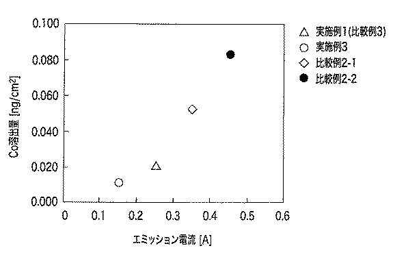
表1に示すように、本発明の範囲内の実施例1〜3の各磁気記録媒体については、Co溶出量を低いレベルに抑えることができていることが判る。これは、実施例1〜3については、いずれも、適正なエチレンガス流量及びエミッション電流により、DCL膜中に適正な量のHが取り込まれ、Hを介した緻密な立体構造が形成されたためと考えられる。 As shown in Table 1, it can be seen that for each of the magnetic recording media of Examples 1 to 3 within the scope of the present invention, the Co elution amount can be suppressed to a low level. This is because, in Examples 1 to 3, an appropriate amount of H was taken into the DCL film by an appropriate ethylene gas flow rate and emission current, and a dense three-dimensional structure via H was formed. Conceivable.
これに対し、本発明の範囲外の比較例1〜4の各磁気記録媒体については、Co溶出量を低いレベルに抑えることができていないことが判る。 On the other hand, it can be seen that in each of the magnetic recording media of Comparative Examples 1 to 4 outside the scope of the present invention, the Co elution amount cannot be suppressed to a low level.
比較例1〜4を個別にみると、比較例1−1については、エチレンガス流量が少なすぎたため、DCL膜がHを介した十分緻密な立体構造にならなかったためであると考えられる。また、比較例1−2については、エチレンガス流量が多すぎたため、DCL膜の構造がポリマー的になってしまったためであると考えられる。 Looking at Comparative Examples 1-4 individually, it is considered that in Comparative Example 1-1, the flow rate of ethylene gas was too small, so that the DCL film did not have a sufficiently dense three-dimensional structure via H. Moreover, about Comparative Example 1-2, since the ethylene gas flow rate was too much, it is considered that the structure of the DCL film has become a polymer.
比較例2−1及び比較例2−2については、いずれも、エミッション電流が大きすぎたため、DCL膜がHを介した十分緻密な立体構造にならなかったためであると考えられる。 In both Comparative Examples 2-1 and 2-2, it is considered that the emission current was too large, and thus the DCL film did not have a sufficiently dense three-dimensional structure via H.
比較例3については、Co溶出量は低く抑えられたものの、エミッション電流が小さすぎたため、通電が十分に行われず、潤滑層との優れた結合性が実現されなかったものと考えられる。 In Comparative Example 3, it was considered that although the elution amount of Co was kept low, the emission current was too small, so that energization was not sufficiently performed and excellent connectivity with the lubricating layer was not realized.
比較例4については、エミッション電流が極端に小さかったため、通電が十分に行われず、プラズマ放電が安定せずに、DLC膜の成膜ができなかったものと考えられる。 In Comparative Example 4, since the emission current was extremely small, it was considered that energization was not performed sufficiently, the plasma discharge was not stabilized, and the DLC film could not be formed.
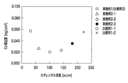
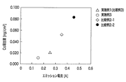
次に、実施例1〜3及び比較例1〜3(比較例4は除く)に関し、Co流出量のエチレンガス流量依存性と、Co流出量のエミッション電流依存性とについての結果を、それぞれ、図1及び図2に示す。 Next, with respect to Examples 1 to 3 and Comparative Examples 1 to 3 (excluding Comparative Example 4), the results about the dependence of the Co outflow amount on the ethylene gas flow rate and the emission current dependence of the Co outflow amount are shown respectively. It shows in FIG.1 and FIG.2.
図1によれば、本発明の範囲内である、所定の炭化水素ガス(エチレンガス)の流量(50sccm以上200sccm以下)の場合には、Co溶出量を低いレベルに抑えることができることが判る。また、図2によれば、本発明の範囲内である、所定のエミッション電流(0.1A以上0.3A以下)の場合には、Co溶出量を低いレベルに抑えることができることが判る。 According to FIG. 1, it can be seen that the Co elution amount can be suppressed to a low level when the flow rate of the predetermined hydrocarbon gas (ethylene gas) (50 sccm or more and 200 sccm or less) is within the scope of the present invention. Further, according to FIG. 2, it is understood that the Co elution amount can be suppressed to a low level in the case of a predetermined emission current (0.1 A or more and 0.3 A or less) which is within the scope of the present invention.
本発明の磁気記録媒体用保護膜の形成方法によれば、特殊な形成工程及び表面処理工程を採用することで、磁気記録層からのCoの溶出を抑制するとともに、膜厚が3nm以下の磁気記録媒体用保護層を形成することができる。従って、本発明は、今後益々、高い記録密度が要請される磁気記録媒体の製造に適用することができる点で有望である。 According to the method for forming a protective film for a magnetic recording medium of the present invention, by adopting a special forming process and a surface treatment process, the elution of Co from the magnetic recording layer is suppressed, and a magnetic film having a film thickness of 3 nm or less is used. A protective layer for a recording medium can be formed. Therefore, the present invention is promising in that it can be applied to the manufacture of a magnetic recording medium that requires a higher recording density.
Claims (4)
(2)工程(1)で形成した保護膜の表面処理工程であって、
(2a)アルゴンガス中でのプラズマ処理、及び
(2b)窒素ガスを含むガス中でのプラズマ処理
を含む表面処理工程と
を含むことを特徴とする磁気記録媒体用保護膜の形成方法。 (1) A step of forming a protective film by a plasma CVD method using a hydrocarbon gas as a raw material on a laminate including a substrate and a metal film layer formed on the substrate, wherein the hydrocarbon gas A protective film forming step in which a flow rate is 50 sccm or more and 200 sccm or less, and a discharge current is 0.1 A or more and 0.3 A or less;
(2) A surface treatment step of the protective film formed in step (1),
A method for forming a protective film for a magnetic recording medium, comprising: (2a) a plasma treatment in argon gas; and (2b) a surface treatment step including plasma treatment in a gas containing nitrogen gas.
前記基体上に形成された金属膜層と、
前記金属膜層上に形成された請求項3に記載の保護膜と
を備えることを特徴とする、磁気記録媒体。 A substrate;
A metal film layer formed on the substrate;
A magnetic recording medium comprising: the protective film according to claim 3 formed on the metal film layer.
Priority Applications (2)
| Application Number | Priority Date | Filing Date | Title |
|---|---|---|---|
| JP2008325922A JP2010146683A (en) | 2008-12-22 | 2008-12-22 | Method of forming protective film, protective film obtained by the method and magnetic recording medium including the protective film |
| US12/644,937 US8334028B2 (en) | 2008-12-22 | 2009-12-22 | Method of forming a protective film |
Applications Claiming Priority (1)
| Application Number | Priority Date | Filing Date | Title |
|---|---|---|---|
| JP2008325922A JP2010146683A (en) | 2008-12-22 | 2008-12-22 | Method of forming protective film, protective film obtained by the method and magnetic recording medium including the protective film |
Publications (1)
| Publication Number | Publication Date |
|---|---|
| JP2010146683A true JP2010146683A (en) | 2010-07-01 |
Family
ID=42285331
Family Applications (1)
| Application Number | Title | Priority Date | Filing Date |
|---|---|---|---|
| JP2008325922A Pending JP2010146683A (en) | 2008-12-22 | 2008-12-22 | Method of forming protective film, protective film obtained by the method and magnetic recording medium including the protective film |
Country Status (2)
| Country | Link |
|---|---|
| US (1) | US8334028B2 (en) |
| JP (1) | JP2010146683A (en) |
Cited By (3)
| Publication number | Priority date | Publication date | Assignee | Title |
|---|---|---|---|---|
| JP2013037745A (en) * | 2011-08-09 | 2013-02-21 | Fuji Electric Co Ltd | Magnetic recording medium |
| DE102013213897A1 (en) | 2012-08-07 | 2014-02-13 | Denso Corporation | Method and apparatus for forming amorphous hard carbon coatings |
| JP2016517996A (en) * | 2013-11-14 | 2016-06-20 | フジ エレクトリック (マレーシア) エスディーエヌ ビーエイチディー | Method for producing carbon-based protective film |
Families Citing this family (2)
| Publication number | Priority date | Publication date | Assignee | Title |
|---|---|---|---|---|
| JP5578215B2 (en) * | 2012-09-14 | 2014-08-27 | 富士電機株式会社 | Method for manufacturing magnetic recording medium |
| JP6360509B2 (en) * | 2016-02-25 | 2018-07-18 | 任天堂株式会社 | Information processing program, information processing system, information processing method, and information processing apparatus |
Citations (2)
| Publication number | Priority date | Publication date | Assignee | Title |
|---|---|---|---|---|
| JP2004280888A (en) * | 2003-03-13 | 2004-10-07 | Tdk Corp | Manufacturing method and device of magnetic recording medium |
| JP2008276898A (en) * | 2007-05-07 | 2008-11-13 | Fujitsu Ltd | Method for manufacturing magnetic recording medium and magnetic recording apparatus |
Family Cites Families (36)
| Publication number | Priority date | Publication date | Assignee | Title |
|---|---|---|---|---|
| JP2532209B2 (en) * | 1986-04-04 | 1996-09-11 | ティーディーケイ株式会社 | Magnetic recording media |
| JP2610469B2 (en) * | 1988-02-26 | 1997-05-14 | 株式会社 半導体エネルギー研究所 | Method for forming carbon or carbon-based coating |
| JPH0291838A (en) * | 1988-09-28 | 1990-03-30 | Fuji Photo Film Co Ltd | Production of magneto-optical recording medium |
| US5053246A (en) * | 1990-03-30 | 1991-10-01 | The Goodyear Tire & Rubber Company | Process for the surface treatment of polymers for reinforcement-to-rubber adhesion |
| JP2915251B2 (en) * | 1993-06-28 | 1999-07-05 | 株式会社日立製作所 | Magnetic recording medium and method of manufacturing the same |
| JP3661949B2 (en) * | 1994-03-11 | 2005-06-22 | 富士写真フイルム株式会社 | Magnetic recording medium |
| US5462784A (en) * | 1994-11-02 | 1995-10-31 | International Business Machines Corporation | Fluorinated diamond-like carbon protective coating for magnetic recording media devices |
| JPH0940494A (en) | 1995-05-19 | 1997-02-10 | Sanyo Electric Co Ltd | Hard carbon film and its formation |
| JP3058066B2 (en) | 1995-11-06 | 2000-07-04 | 富士電機株式会社 | Magnetic recording medium and method of manufacturing the same |
| JPH1053877A (en) | 1996-06-06 | 1998-02-24 | Shimadzu Corp | Thin film forming equipment and functional single thin film |
| KR100296692B1 (en) * | 1996-09-10 | 2001-10-24 | 사토 도리 | Plasma CVD |
| US6066399A (en) * | 1997-03-19 | 2000-05-23 | Sanyo Electric Co., Ltd. | Hard carbon thin film and method of forming the same |
| WO1999014746A1 (en) | 1997-09-17 | 1999-03-25 | Showa Denko K.K. | Magnetic recording medium and method of producing the same |
| US6316062B1 (en) * | 1997-09-17 | 2001-11-13 | Showa Denko K.K. | Magnetic recording medium and method of producing the same |
| EP0903204A3 (en) * | 1997-09-22 | 2002-04-10 | SANYO ELECTRIC Co., Ltd. | Sliding member, inner and outer blades of an electric shaver and film-forming method |
| US5981000A (en) * | 1997-10-14 | 1999-11-09 | International Business Machines Corporation | Method for fabricating a thermally stable diamond-like carbon film |
| JP2000268357A (en) | 1999-03-12 | 2000-09-29 | Hitachi Ltd | Method and apparatus for manufacturing magnetic recording medium |
| JP2001034939A (en) * | 1999-07-16 | 2001-02-09 | Fuji Electric Co Ltd | Master magnetic information carrier, method of manufacturing the same, and method of manufacturing magnetic recording medium |
| JP2001043530A (en) * | 1999-07-28 | 2001-02-16 | Anelva Corp | Method of forming protective film for information recording disk and apparatus for forming thin film for information recording disk |
| JP2001084554A (en) * | 1999-09-14 | 2001-03-30 | Fuji Photo Film Co Ltd | Magnetic recording medium |
| JP2001126233A (en) | 1999-10-26 | 2001-05-11 | Fuji Electric Co Ltd | Manufacturing method of magnetic recording medium |
| JP4034924B2 (en) * | 2000-06-13 | 2008-01-16 | 松下電器産業株式会社 | Magnetic transfer device |
| JP4161540B2 (en) * | 2000-06-28 | 2008-10-08 | 富士電機デバイステクノロジー株式会社 | Magnetic transfer method for perpendicular magnetic recording medium |
| JP4491934B2 (en) * | 2000-08-10 | 2010-06-30 | 富士電機デバイステクノロジー株式会社 | Method for manufacturing thin film magnetic recording medium |
| US7147943B2 (en) * | 2000-09-28 | 2006-12-12 | Hitachi Global Storage Technologies Japan, Ltd. | Magnetic recording medium, the manufacturing method and magnetic recording apparatus using the same |
| JP2003296922A (en) * | 2002-04-02 | 2003-10-17 | Fuji Photo Film Co Ltd | Magnetic recording medium |
| JP4031944B2 (en) * | 2002-04-08 | 2008-01-09 | 株式会社日立グローバルストレージテクノロジーズ | Magnetic disk design method and magnetic disk device design method |
| JP3755765B2 (en) * | 2003-02-12 | 2006-03-15 | Hoya株式会社 | Manufacturing method of magnetic disk |
| JP2004288327A (en) | 2003-03-24 | 2004-10-14 | Fuji Electric Device Technology Co Ltd | Magnetic recording medium and method of manufacturing the same |
| JP2005158092A (en) | 2003-11-20 | 2005-06-16 | Fujitsu Ltd | Magnetic recording medium, magnetic storage device, and method of manufacturing magnetic recording medium |
| JP4812254B2 (en) * | 2004-01-08 | 2011-11-09 | 富士電機株式会社 | Perpendicular magnetic recording medium and manufacturing method thereof |
| WO2006019176A1 (en) * | 2004-08-19 | 2006-02-23 | Showa Denko K.K. | Magnetic recording medium and production process thereof |
| JP4839723B2 (en) * | 2005-08-10 | 2011-12-21 | 富士電機株式会社 | Protective film forming method and magnetic recording medium provided with the protective film |
| JP5430826B2 (en) * | 2006-03-08 | 2014-03-05 | シャープ株式会社 | Nitride semiconductor laser device |
| JP2007265586A (en) | 2006-03-30 | 2007-10-11 | Hoya Corp | Magnetic disk and its manufacturing method |
| JP5093686B2 (en) * | 2008-08-27 | 2012-12-12 | 富士電機株式会社 | Method for forming protective film for magnetic recording medium |
-
2008
- 2008-12-22 JP JP2008325922A patent/JP2010146683A/en active Pending
-
2009
- 2009-12-22 US US12/644,937 patent/US8334028B2/en active Active
Patent Citations (2)
| Publication number | Priority date | Publication date | Assignee | Title |
|---|---|---|---|---|
| JP2004280888A (en) * | 2003-03-13 | 2004-10-07 | Tdk Corp | Manufacturing method and device of magnetic recording medium |
| JP2008276898A (en) * | 2007-05-07 | 2008-11-13 | Fujitsu Ltd | Method for manufacturing magnetic recording medium and magnetic recording apparatus |
Cited By (4)
| Publication number | Priority date | Publication date | Assignee | Title |
|---|---|---|---|---|
| JP2013037745A (en) * | 2011-08-09 | 2013-02-21 | Fuji Electric Co Ltd | Magnetic recording medium |
| US9196282B2 (en) | 2011-08-09 | 2015-11-24 | Fuji Electric Co., Ltd. | Magnetic recording medium |
| DE102013213897A1 (en) | 2012-08-07 | 2014-02-13 | Denso Corporation | Method and apparatus for forming amorphous hard carbon coatings |
| JP2016517996A (en) * | 2013-11-14 | 2016-06-20 | フジ エレクトリック (マレーシア) エスディーエヌ ビーエイチディー | Method for producing carbon-based protective film |
Also Published As
| Publication number | Publication date |
|---|---|
| US8334028B2 (en) | 2012-12-18 |
| US20100167090A1 (en) | 2010-07-01 |
Similar Documents
| Publication | Publication Date | Title |
|---|---|---|
| JP5093686B2 (en) | Method for forming protective film for magnetic recording medium | |
| CN104167215B (en) | Magnetic recording medium and its manufacturing method | |
| US8888966B2 (en) | Protective film mainly composed of a tetrahedral amorphous carbon film and a magnetic recording medium having the protective film | |
| US20130337194A1 (en) | Covalently bound monolayer for a protective carbon overcoat | |
| JP2010146683A (en) | Method of forming protective film, protective film obtained by the method and magnetic recording medium including the protective film | |
| JP5605169B2 (en) | Protective film and magnetic recording medium provided with the protective film | |
| WO2004070712A1 (en) | Magnetic recording medium and method for producing the same, magnetic medium substrate being employed therein, and magnetic storage device | |
| JP6186500B2 (en) | Method for producing carbon-based protective film | |
| JP6089740B2 (en) | Recording / reproducing method of magnetic recording medium | |
| JP5808511B2 (en) | Magnetic recording medium and method for manufacturing protective film thereof | |
| JP4417336B2 (en) | Method for manufacturing magnetic recording medium | |
| JP2009080897A (en) | Manufacturing method of perpendicular magnetic recording disk and perpendicular magnetic recording disk | |
| JP2010272183A (en) | Perpendicular magnetic recording medium and method for manufacturing discrete track medium and the like | |
| JP2026037869A (en) | Magnetic recording medium manufacturing method and magnetic recording/reproducing device | |
| CN101138025A (en) | Manufacturing method of magnetic recording medium, magnetic recording medium, and magnetic recording and reproducing apparatus | |
| CN101297358A (en) | Method for manufacturing magnetic recording medium, and magnetic read/write apparatus | |
| JP2009245545A (en) | Manufacturing method of vertical magnetic recording medium | |
| JP2009116975A (en) | Perpendicular magnetic recording medium and manufacturing method thereof |
Legal Events
| Date | Code | Title | Description |
|---|---|---|---|
| A711 | Notification of change in applicant |
Free format text: JAPANESE INTERMEDIATE CODE: A712 Effective date: 20110722 |
|
| A621 | Written request for application examination |
Free format text: JAPANESE INTERMEDIATE CODE: A621 Effective date: 20110913 |
|
| A977 | Report on retrieval |
Free format text: JAPANESE INTERMEDIATE CODE: A971007 Effective date: 20120621 |
|
| A131 | Notification of reasons for refusal |
Free format text: JAPANESE INTERMEDIATE CODE: A131 Effective date: 20120629 |
|
| A521 | Request for written amendment filed |
Free format text: JAPANESE INTERMEDIATE CODE: A523 Effective date: 20120827 |
|
| A02 | Decision of refusal |
Free format text: JAPANESE INTERMEDIATE CODE: A02 Effective date: 20130208 |