US9618694B2 - Optical waveguide and arrayed waveguide grating - Google Patents
Optical waveguide and arrayed waveguide grating Download PDFInfo
- Publication number
- US9618694B2 US9618694B2 US13/698,573 US201113698573A US9618694B2 US 9618694 B2 US9618694 B2 US 9618694B2 US 201113698573 A US201113698573 A US 201113698573A US 9618694 B2 US9618694 B2 US 9618694B2
- Authority
- US
- United States
- Prior art keywords
- waveguide
- grating
- refractive index
- region
- light
- Prior art date
- Legal status (The legal status is an assumption and is not a legal conclusion. Google has not performed a legal analysis and makes no representation as to the accuracy of the status listed.)
- Active, expires
Links
- 230000003287 optical effect Effects 0.000 title abstract description 67
- 238000009826 distribution Methods 0.000 claims description 17
- 238000004519 manufacturing process Methods 0.000 abstract description 16
- 238000000034 method Methods 0.000 abstract description 16
- 238000003780 insertion Methods 0.000 abstract description 10
- 230000037431 insertion Effects 0.000 abstract description 10
- 230000000694 effects Effects 0.000 description 27
- LFEUVBZXUFMACD-UHFFFAOYSA-H lead(2+);trioxido(oxo)-$l^{5}-arsane Chemical compound [Pb+2].[Pb+2].[Pb+2].[O-][As]([O-])([O-])=O.[O-][As]([O-])([O-])=O LFEUVBZXUFMACD-UHFFFAOYSA-H 0.000 description 27
- 239000000463 material Substances 0.000 description 22
- 238000004364 calculation method Methods 0.000 description 15
- 239000010410 layer Substances 0.000 description 14
- 239000012792 core layer Substances 0.000 description 13
- VYPSYNLAJGMNEJ-UHFFFAOYSA-N Silicium dioxide Chemical compound O=[Si]=O VYPSYNLAJGMNEJ-UHFFFAOYSA-N 0.000 description 7
- 230000015572 biosynthetic process Effects 0.000 description 6
- 239000011162 core material Substances 0.000 description 5
- 238000009792 diffusion process Methods 0.000 description 5
- 239000011347 resin Substances 0.000 description 5
- 229920005989 resin Polymers 0.000 description 5
- 230000001066 destructive effect Effects 0.000 description 4
- 239000010419 fine particle Substances 0.000 description 4
- 230000005855 radiation Effects 0.000 description 4
- 238000005530 etching Methods 0.000 description 3
- 238000001459 lithography Methods 0.000 description 3
- 239000004576 sand Substances 0.000 description 3
- 230000007704 transition Effects 0.000 description 3
- 229910052681 coesite Inorganic materials 0.000 description 2
- 229910052906 cristobalite Inorganic materials 0.000 description 2
- 238000000151 deposition Methods 0.000 description 2
- YBMRDBCBODYGJE-UHFFFAOYSA-N germanium oxide Inorganic materials O=[Ge]=O YBMRDBCBODYGJE-UHFFFAOYSA-N 0.000 description 2
- 230000007062 hydrolysis Effects 0.000 description 2
- 238000006460 hydrolysis reaction Methods 0.000 description 2
- 230000031700 light absorption Effects 0.000 description 2
- 230000001902 propagating effect Effects 0.000 description 2
- 239000000377 silicon dioxide Substances 0.000 description 2
- 229910052682 stishovite Inorganic materials 0.000 description 2
- 229910052905 tridymite Inorganic materials 0.000 description 2
- 239000006229 carbon black Substances 0.000 description 1
- 230000001419 dependent effect Effects 0.000 description 1
- 239000003822 epoxy resin Substances 0.000 description 1
- 230000002452 interceptive effect Effects 0.000 description 1
- 239000002184 metal Substances 0.000 description 1
- 238000010606 normalization Methods 0.000 description 1
- 229920000647 polyepoxide Polymers 0.000 description 1
- 230000000644 propagated effect Effects 0.000 description 1
- 229920002050 silicone resin Polymers 0.000 description 1
- 238000004088 simulation Methods 0.000 description 1
- 239000000758 substrate Substances 0.000 description 1
Images


Classifications
-
- G—PHYSICS
- G02—OPTICS
- G02B—OPTICAL ELEMENTS, SYSTEMS OR APPARATUS
- G02B6/00—Light guides; Structural details of arrangements comprising light guides and other optical elements, e.g. couplings
- G02B6/10—Light guides; Structural details of arrangements comprising light guides and other optical elements, e.g. couplings of the optical waveguide type
- G02B6/12—Light guides; Structural details of arrangements comprising light guides and other optical elements, e.g. couplings of the optical waveguide type of the integrated circuit kind
- G02B6/12007—Light guides; Structural details of arrangements comprising light guides and other optical elements, e.g. couplings of the optical waveguide type of the integrated circuit kind forming wavelength selective elements, e.g. multiplexer, demultiplexer
- G02B6/12009—Light guides; Structural details of arrangements comprising light guides and other optical elements, e.g. couplings of the optical waveguide type of the integrated circuit kind forming wavelength selective elements, e.g. multiplexer, demultiplexer comprising arrayed waveguide grating [AWG] devices, i.e. with a phased array of waveguides
- G02B6/12014—Light guides; Structural details of arrangements comprising light guides and other optical elements, e.g. couplings of the optical waveguide type of the integrated circuit kind forming wavelength selective elements, e.g. multiplexer, demultiplexer comprising arrayed waveguide grating [AWG] devices, i.e. with a phased array of waveguides characterised by the wavefront splitting or combining section, e.g. grooves or optical elements in a slab waveguide
-
- G—PHYSICS
- G02—OPTICS
- G02B—OPTICAL ELEMENTS, SYSTEMS OR APPARATUS
- G02B6/00—Light guides; Structural details of arrangements comprising light guides and other optical elements, e.g. couplings
- G02B6/10—Light guides; Structural details of arrangements comprising light guides and other optical elements, e.g. couplings of the optical waveguide type
- G02B6/12—Light guides; Structural details of arrangements comprising light guides and other optical elements, e.g. couplings of the optical waveguide type of the integrated circuit kind
- G02B6/12007—Light guides; Structural details of arrangements comprising light guides and other optical elements, e.g. couplings of the optical waveguide type of the integrated circuit kind forming wavelength selective elements, e.g. multiplexer, demultiplexer
- G02B6/12009—Light guides; Structural details of arrangements comprising light guides and other optical elements, e.g. couplings of the optical waveguide type of the integrated circuit kind forming wavelength selective elements, e.g. multiplexer, demultiplexer comprising arrayed waveguide grating [AWG] devices, i.e. with a phased array of waveguides
- G02B6/12011—Light guides; Structural details of arrangements comprising light guides and other optical elements, e.g. couplings of the optical waveguide type of the integrated circuit kind forming wavelength selective elements, e.g. multiplexer, demultiplexer comprising arrayed waveguide grating [AWG] devices, i.e. with a phased array of waveguides characterised by the arrayed waveguides, e.g. comprising a filled groove in the array section
-
- G—PHYSICS
- G02—OPTICS
- G02B—OPTICAL ELEMENTS, SYSTEMS OR APPARATUS
- G02B6/00—Light guides; Structural details of arrangements comprising light guides and other optical elements, e.g. couplings
- G02B6/24—Coupling light guides
- G02B6/26—Optical coupling means
- G02B6/28—Optical coupling means having data bus means, i.e. plural waveguides interconnected and providing an inherently bidirectional system by mixing and splitting signals
- G02B6/293—Optical coupling means having data bus means, i.e. plural waveguides interconnected and providing an inherently bidirectional system by mixing and splitting signals with wavelength selective means
- G02B6/29344—Optical coupling means having data bus means, i.e. plural waveguides interconnected and providing an inherently bidirectional system by mixing and splitting signals with wavelength selective means operating by modal interference or beating, i.e. of transverse modes, e.g. zero-gap directional coupler, MMI
-
- G—PHYSICS
- G02—OPTICS
- G02B—OPTICAL ELEMENTS, SYSTEMS OR APPARATUS
- G02B6/00—Light guides; Structural details of arrangements comprising light guides and other optical elements, e.g. couplings
- G02B6/24—Coupling light guides
- G02B6/26—Optical coupling means
- G02B6/28—Optical coupling means having data bus means, i.e. plural waveguides interconnected and providing an inherently bidirectional system by mixing and splitting signals
- G02B6/2804—Optical coupling means having data bus means, i.e. plural waveguides interconnected and providing an inherently bidirectional system by mixing and splitting signals forming multipart couplers without wavelength selective elements, e.g. "T" couplers, star couplers
- G02B6/2808—Optical coupling means having data bus means, i.e. plural waveguides interconnected and providing an inherently bidirectional system by mixing and splitting signals forming multipart couplers without wavelength selective elements, e.g. "T" couplers, star couplers using a mixing element which evenly distributes an input signal over a number of outputs
- G02B6/2813—Optical coupling means having data bus means, i.e. plural waveguides interconnected and providing an inherently bidirectional system by mixing and splitting signals forming multipart couplers without wavelength selective elements, e.g. "T" couplers, star couplers using a mixing element which evenly distributes an input signal over a number of outputs based on multimode interference effect, i.e. self-imaging
Definitions
- the present disclosure relates to an optical waveguide and an arrayed waveguide grating, which can reduce insertion loss when light enters from a slab waveguide toward an arrayed waveguide or when the light enters from the arrayed waveguide toward the slab waveguide.
- Patent Documents 1 to 6 disclose such a connection structure between a slab waveguide and an arrayed waveguide that when light enters from a slab waveguide toward an arrayed waveguide, the light does not radiate in a clad layer as a radiation mode between the arrayed waveguides adjacent to each other.
- a transition region where the refractive index of the waveguide gradually changes from the slab waveguide toward the arrayed waveguide is disposed.
- a slope portion is disposed between the slab waveguide and the arrayed waveguide.
- a core layer and a plurality of island-shaped regions are arranged in the slab waveguide.
- the refractive index of the island-shaped region is smaller than the refractive index of the core layer.
- the island-shaped regions face a clad layer provided between the adjacent arrayed waveguides. The width of the island-shaped region in a direction substantially vertical to a light propagation direction becomes narrower from the slab waveguide toward the arrayed waveguide.
- Light passing through the core layer provided between the island-shaped regions adjacent to each other propagates toward the arrayed waveguide without changing the propagation direction.
- Light passing through the island-shaped region changes the propagation direction due to a tapered shape of the island-shaped region and propagates toward the arrayed waveguide.
- the tapered shape and the position of the island-shaped region are optimized, whereby the light is concentrated on the arrayed waveguide and propagates in the arrayed waveguide as a propagation mode.
- the present disclosure has the purpose of providing an optical waveguide and an arrayed waveguide grating, which do not increase the circuit size, do not make the circuit design and manufacturing difficult, and can reduce insertion loss when light enters from a slab waveguide toward an arrayed waveguide or when the light enters from the arrayed waveguide toward the slab waveguide.
- a grating is formed in the slab waveguide, and an end of the arrayed waveguide is disposed at a position where a constructive interference portion of a self-image of the grating is formed.
- the present disclosure provides an optical waveguide which is provided with a slab waveguide in which a grating is formed therein at a distance from an end and an arrayed waveguide whose end is connected to an end of the slab waveguide at a position where a constructive interference portion of a self-image of the grating is formed.
- the self-image of the grating is formed according to wavelength of light and a period of the grating formed in the slab waveguide.
- the end of the arrayed waveguide is disposed at the position where the constructive interference portion of the self-image of the grating is formed, so that when light enters from the slab waveguide toward the arrayed waveguide, the light is concentrated on the arrayed waveguide and propagates in the arrayed waveguide as a propagation mode.
- the size of an optical waveguide is not increased, the design and manufacturing is not made difficult, and insertion loss can be reduced when the light enters from the slab waveguide toward the arrayed waveguide or when the light enters from the arrayed waveguide toward the slab waveguide.
- the present disclosure provides an optical waveguide in which the grating is a phase grating.
- the incident light is diffracted due to a phase difference given to incident light, and therefore, loss of the incident light can be reduced.
- the present disclosure provides an optical waveguide in which the phase difference given to the incident light by the phase grating is approximately 90 degrees.
- the self-image of the phase grating is clearly formed.
- the present disclosure provides an optical waveguide in which the phase difference given to the incident light by the phase grating is approximately 180 degrees.
- the self-image of the phase grating is clearly formed.
- the present disclosure provides an optical waveguide in which the phase grating is provided with refractive index difference regions which are disposed in the slab waveguide at a distance in a direction substantially vertical to a light propagation direction and have a refractive index different from the refractive indices of other regions in the slab waveguide.
- the phase grating can be easily formed in the slab waveguide.
- the present disclosure provides an optical waveguide in which the refractive index difference regions adjacent to each other are connected by a region having a refractive index equal to the refractive index of the refractive index difference region, and the refractive index difference regions are integral with each other across the entire phase grating.
- the phase grating can be easily formed in the slab waveguide.
- the present disclosure provides an optical waveguide which is provided with one or more first input/output waveguide(s), an optical waveguide where an end of the slab waveguide on an opposite side of the arrayed waveguide is connected to an end of the first input/output waveguide, a second slab waveguide connected to an end of the arrayed waveguide on an opposite side of the slab waveguide, and one or more second input/output waveguide(s) connected to an end of the second slab waveguide on the opposite side of the arrayed waveguide.
- the size of the arrayed waveguide grating is not increased, the design and manufacturing is not made difficult, and the insertion loss can be reduced when light enters from the slab waveguide toward the arrayed waveguide or when the light enters from the arrayed waveguide toward the slab waveguide.
- the present disclosure provides an arrayed waveguide grating which is provided with two or more first input/output waveguides, a first slab waveguide connected to an end of the first input/output waveguides, an arrayed waveguide connected to an end of the first slab waveguide on an opposite side of the first input/output waveguides, a second slab waveguide connected to an end of the arrayed waveguide on an opposite side of the first slab waveguide, and one or more second input/output waveguide(s) connected to an end of the second slab waveguide on an opposite side of the arrayed waveguide, wherein in the first slab waveguide, a grating is formed therein at a distance from an end, and an end of the arrayed waveguide is connected to a position deviated from a position where a constructive interference portion of a self-image of the grating is formed so that a light intensity distribution from the first input/output waveguides is substantially uniform when light enters from the second input/output waveguide toward the first input/output
- loss in two or more of the first input/output waveguides can be uniformed in a demultiplexer through which light enters from the second input/output waveguide toward the first input/output waveguide or a multiplexer through which light enters from the first input/output waveguide toward the second input/output waveguide.
- the present disclosure provides an arrayed waveguide grating in which the grating is a phase grating.
- the incident light is diffracted due to a phase difference given to the incident light, and therefore, loss of the incident light can be reduced.
- the present disclosure provides an arrayed waveguide grating in which the phase difference given to the incident light by the phase grating is approximately 90 degrees.
- the self-image of the phase grating is clearly formed.
- the present disclosure provides an arrayed waveguide grating in which the phase difference given to the incident light by the phase grating is approximately 180 degrees.
- the self-image of the phase grating is clearly formed.
- the present disclosure provides an arrayed waveguide grating in which the phase grating is provided with refractive index difference regions which are disposed in the slab waveguide at a distance in a direction substantially vertical to a light propagation direction and have a refractive index different from the refractive indices of other regions in the slab waveguide.
- the phase grating can be easily formed in the slab waveguide.
- the present disclosure provides an arrayed waveguide grating in which the refractive index difference regions adjacent to each other are connected by a region having a refractive index equal to the refractive index of the refractive index difference regions, and the refractive index difference regions are integral with each other across the entire phase grating.
- the phase grating can be easily formed in the slab waveguide.
- the present disclosure can provide an optical waveguide and an arrayed waveguide grating, which do not increase the circuit size, do not make the circuit design and manufacturing difficult, and can reduce insertion loss when light enters from a slab waveguide toward an arrayed waveguide or when the light enters from the arrayed waveguide toward the slab waveguide.
- FIG. 1 is a view showing a phenomenon of Talbot effect.
- FIG. 2 is a view showing the phenomenon of the Talbot effect.
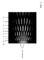
- FIG. 3 is a view showing calculation results of the Talbot effect.
- FIG. 4 is a view showing calculation results of the Talbot effect.
- FIG. 5 is a view showing calculation results of the Talbot effect.
- FIGS. 6A, 6B and 6C are views showing a positional relationship between a phase grating of a slab waveguide and an incident end of an arrayed waveguide.
- FIG. 7 is a view showing the calculation results of the Talbot effect.
- FIG. 8 is a view showing a positional relationship between the phase grating of the slab waveguide and the incident end of the arrayed waveguide.
- FIG. 9 is a view showing a structure of an optical waveguide.
- FIG. 10 is a view showing a method of manufacturing the optical waveguide using ultraviolet irradiation.
- FIG. 11 is a view showing the method of manufacturing the optical waveguide using ultraviolet irradiation.
- FIGS. 12A, 12B, 12C and 12D are views showing a structure of the optical waveguide.
- FIGS. 13A and 13B are views showing a structure of the optical waveguide.
- FIGS. 14A, 14B and 14C are views showing a structure of the optical waveguide.
- FIG. 15 is a view showing loss distributions between output channels.
- FIG. 16 is a view showing a relationship between an interference region length and a minimum loss.
- FIG. 17 is a view showing a relationship between the interference region length and loss variation between the output channels.
- an optical waveguide which can reduce insertion loss when light enters from a slab waveguide toward an arrayed waveguide or when the light enters from the arrayed waveguide toward the slab waveguide will be described based on the phenomenon and the calculation results of the Talbot effect.
- the Talbot effect means that diffracted lights interfere with each other when light enters a grating, whereby a light intensity distribution similar to a pattern of the grating is realized as a self-image of the grating at a position apart from the grating with a distance specified according to the wavelength of the light and a period of the grating, and the Talbot effect is applied to a Talbot interferometer.
- FIGS. 1 and 2 are views showing the phenomenon of the Talbot effect.
- Gratings GP 1 and GP 2 are phase gratings giving a phase difference to incident light
- a grating GA is an amplitude grating giving an intensity difference to the incident light.
- the phenomenon of the Talbot effect associated with the phase grating GP 1 is shown in an upper half of FIG. 1
- the phenomenon of the Talbot effect associated with the amplitude grating GA is shown in a lower half of FIG. 1
- the phenomenon of the Talbot effect associated with the phase grating GP 2 is shown in FIG. 2 .
- Each period of the phase gratings GP 1 and GP 2 and the amplitude grating GA is d.
- the phase difference given to the incident light by the phase grating GP 1 is 90°.
- the phase difference given to the incident light by the phase grating GP 2 is 180°.
- the wavelength of the incident light is ⁇ .
- the incident light enters as parallel light in the z-axis direction as shown by arrows at the left ends of FIGS. 1 and 2 .
- the intensity period of the self-image SP 1 of the phase grating GP 1 is d.
- the phenomenon of the Talbot effect associated with the amplitude grating GA will be described.
- the self-images SA of the amplitude grating GA are formed at positions other than the positions of m ⁇ 2, 4, 6, 8, . . . , 4n+2, 4n+4, . . . , the self-images SA are not clearly formed, and the boundary between the constructive interference portion and the destructive interference portion is not clear.
- the intensity period of the self-image SA of the amplitude grating GA is d.
- the phenomenon of the Talbot effect associated with the phase grating GP 2 will be described.
- n is an integer of not less than 0.
- self-images SP 2 of the phase grating GP 2 are clearly formed as shown by diagonal lines and white portions.
- the intensity period of the self-image SP 2 of the phase grating GP 2 is d/2. The self-image SP 2 does not shift for each order.
- the phase gratings GP 1 and GP 2 change the speed of light according to the position of their x coordinate and give a phase difference to incident light.
- the amplitude grating GA changes absorption of light according to the position of the x coordinate and gives an intensity difference to the incident light. Accordingly, when the optical waveguide according to the present disclosure is applied to an arrayed waveguide grating described in an Embodiment 4, the phase gratings GP 1 and GP 2 are preferably used in order to reduce loss of light.
- phase gratings GP 1 and GP 2 will be described in detail, and in the case of using the amplitude grating GA, portions different from the case of using the phase gratings GP 1 and GP 2 will be briefly described.
- FIG. 3 is a view showing calculation results of the Talbot effect of the phase grating GP 1 .
- incident light is parallel light
- the incident light in FIG. 3 is diffusion light in consideration that the light propagating in the slab waveguide is not parallel light but diffusion light.
- the incident light enters as diffusion light in a right direction as shown by arrows at the left end of FIG. 3 .
- FIG. 4 is a view showing calculation results of the Talbot effect of the phase grating GP 2 .
- incident light is parallel light.
- the incident light enters as parallel light in a right direction as shown by arrows at the left end of FIG. 4 .
- the closer to the positions of m 1, 3, 5, 7, . . . , 4n+1, 4n+3, .
- the more clearly the self-image SP 1 of the phase grating GP 1 are formed, and the closer to the positions of m 2, 4, 6, 8, . . . , 4n+2, 4n+4, . . . , the less clearly the self-image SP 1 of the phase grating GP 1 is formed.
- FIG. 3 When FIG. 3 is seen as a whole, the black and white gradation is spread in the vertical direction of FIG. 3 as it progresses in the right side direction.
- phase grating GP 2 is formed of a material having a small refractive index difference such as a core material and a clad material
- the phase grating GP 2 is elongated in a light propagation direction, light propagating in a portion having a low refractive index couples to a portion having a high refractive index as the propagation distance becomes longer, and the intensity distribution occurs at an end of the phase grating GP 2 .
- FIG. 5 is a view showing calculation results of the Talbot effect on the phase grating GP giving various phase differences to incident light.
- the phase differences given to the incident light by the phase grating GP are ⁇ /8, ⁇ /4, ⁇ /2, 3 ⁇ /4, 7 ⁇ /8, ⁇ , ⁇ /12, ⁇ /6, and ⁇ /3 at the left end of the upper stage, the center of the upper stage, the right end of the upper stage, the left end of the intermediate stage, the center of the intermediate stage, the right end of the intermediate stage, the left end of the lower stage, the center of the lower stage, and the right end of the lower stage, respectively.
- FIG. 5 is a view showing calculation results of the Talbot effect on the phase grating GP giving various phase differences to incident light.
- the phase differences given to the incident light by the phase grating GP are ⁇ /8, ⁇ /4, ⁇ /2, 3 ⁇ /4, 7 ⁇ /8, ⁇ , ⁇ /12, ⁇ /6, and ⁇ /3 at the left end of the upper stage,
- the incident light is parallel light, and the phase grating GP is disposed at the left end of each drawing.
- the phase difference given to the incident light by the phase grating GP may be a phase difference other than the above phase differences in FIG. 5 .
- FIGS. 6A, 6B and 6C are views showing a positional relationship between the phase grating GP 1 or GP 2 of a slab waveguide 1 and an end of an arrayed waveguide 2 .
- the respective left sides of FIGS. 6A to 6C show the overall configuration of the optical waveguide, the respective right sides of FIGS. 6A and 6B show the self-image SP 1 of the phase grating GP 1 , the right side of FIG.
- FIGS. 6C shows the self-image SP 2 of the phase grating GP 2 , and in each of FIGS. 6A to 6C , the left and right side views are aligned in the vertical direction of FIGS. 6A, 6B and 6C by alternate long and short dashed lines.
- the positional relationship between the phase grating GP 1 of the slab waveguide 1 and the end of the arrayed waveguide 2 is different from each other.
- the slab waveguide 1 is constituted of an incident region IN, the phase grating GP 1 or GP 2 , and an interference region IF.
- the incident region IN is disposed on the incident side of the slab waveguide 1 , and incident light propagates in the incident region IN.
- the phase grating GP 1 or GP 2 is provided in the slab waveguide 1 and disposed between the incident region IN and the interference region IF, and formed from a region shown by diagonal lines and a region shown by a white portion, which have different refractive indices.
- the refractive index of the region shown by the diagonal lines may be larger or smaller than the refractive index of the region shown by the white portion.
- Incident light propagates in the region with a large refractive index at low speed and propagates in the region with a small refractive index at high speed.
- the phase grating GP 1 or GP 2 changes the speed of light according to the position in the vertical direction of FIGS. 6A, 6B and 6C and gives a phase difference to the incident light.
- the interference region IF is disposed at an end of the slab waveguide 1 on the arrayed waveguide 2 side, and diffraction light is propagated in the interference region IF.
- the arrayed waveguide 2 is connected to the interference region IF of the slab waveguide 1 at a constructive interference portion shown by the white portion of the self-image SP 1 of the phase grating GP 1 or the self-image SP 2 of the phase grating GP 2 .
- the diffraction light since the diffraction light is intensively distributed in the constructive interference portion shown by the white portion of the self-image SP 1 of the phase grating GP 1 or the self-image SP 2 of the phase grating GP 2 , the diffraction light propagates in the arrayed waveguide 2 as a propagation mode.
- the diffraction light Since the diffraction light is hardly distributed in a destructive interference portion shown by the diagonal lines of the self-image SP 1 of the phase grating GP 1 or the self-image SP 2 of the phase grating GP 2 , the diffraction light does not radiate in the clad layer as a radiation mode.
- a plurality of the array waveguides 2 are connected; however, only one waveguide may be connected.
- FIG. 6A at the position corresponding to the region shown by the diagonal lines of the phase grating GP 1 , the constructive interference portion shown by the white portion of the self-image SP 1 of the phase grating GP 1 is formed, and the end of the arrayed waveguide 2 is connected.
- FIG. 6B at the position corresponding to the region shown by the white portion of the phase grating GP 1 , the constructive interference portion shown by the white portion of the self-image SP 1 of the phase grating GP 1 is formed, and the end of the arrayed waveguide 2 is connected.
- the constructive interference portion shown by the white portion of the self-image SP 2 of the phase grating GP 2 is formed, and the end of the arrayed waveguide 2 is connected.
- the period of the phase grating GP 1 is the same as the period of the arrayed waveguide 2 in FIGS. 6A and 6B
- the period of the phase grating GP 2 is twice the period of the arrayed waveguide 2 in FIG. 6C .
- the width in the direction substantially vertical to the light propagation direction of the region with a small refractive index of the phase grating GP 2 of FIG. 6C is twice the width in the direction substantially vertical to the light propagation direction of the region with a small refractive index of the phase grating GP 1 of FIGS. 6A and 6B .
- a light propagation direction width L 1 of the phase grating GP 2 is a length corresponding to the phase difference ⁇ , and the light propagation direction width L 1 of the phase grating GP 1 is a length corresponding to the phase difference ⁇ /2; therefore, the width in the direction substantially parallel to the light propagation direction of the region with a small refractive index of the phase grating GP 2 is twice the width in the direction substantially parallel to the light propagation direction of the region with a small refractive index of the phase grating GP 1 .
- the region with a small refractive index thus increases, light radiation loss increases when light propagates in the region with a small refractive index.
- phase grating GP 2 a value obtained by dividing the width of the region with a large refractive index in the direction substantially vertical to the light propagation direction by the period of the phase grating GP 2 in the direction substantially vertical to the light propagation direction is defined as duty ratio.
- FIG. 7 is a view showing the calculation results of the Talbot effect of the phase grating GP 2 with various duty ratios. The duty ratios of the phase grating GP 2 at the left end, the center, and the right end of FIG. 7 are 0.75, 0.5, and 0.25, respectively.
- incident light is parallel light, and the phase grating GP 2 is disposed at the left end of each drawing.
- the self-image SP 1 , SP 2 , or SA of the grating GP 1 , GP 2 , or GA is formed according to the wavelength ⁇ of the incident light and the period of the grating GP 1 , GP 2 or GA formed in the slab waveguide 1 .
- the end of the arrayed waveguide 2 is disposed at the position where the constructive interference portion of the self-image SP 1 , SP 2 , or SA of the grating GP 1 , GP 2 or GA is formed, whereby the light is concentrated on the arrayed waveguide 2 and propagates as a propagation mode when light enters from the slab waveguide 1 toward the arrayed waveguide 2 .
- each end of the branched arrayed waveguides 2 is disposed at the position where the constructive interference portion is formed.
- a method of designing an optical waveguide will be described. First, a method of setting a light propagation direction width L 1 of phase gratings GP 1 and GP 2 will be described, next, a method of setting a light propagation direction width L 2 of an interference region IF will be described, and finally, a method of setting a position of an end of an arrayed waveguide 2 will be described.
- the light propagation direction width L 1 of the phase grating GP 1 is set so that a phase difference given to light by the phase grating GP 1 is preferably 80 to 100°, more preferably 90°.
- the light propagation direction width L 1 of the phase grating GP 2 is set so that a phase difference given to light by the phase grating GP 2 is preferably 170 to 190°, more preferably 180°.
- Wavelength of light in vacuum is represented by ⁇
- a refractive index of a region with a large refractive index is represented by n
- the refractive index of a region with a small refractive index is represented by n ⁇ n
- L 1 is preferably set to be ⁇ /(4n ⁇ ) so that the phase difference given to light by the phase grating GP 1 is 90°.
- L 1 is preferably set to be about 35 ⁇ m so that the phase difference given to light by the phase grating GP 1 is 90°.
- L 1 is preferably set to be ⁇ /(2n ⁇ ) so that the phase difference given to light by the phase grating GP 2 is 180°.
- L 1 is preferably set to be about 70 ⁇ m so that the phase difference given to light by the phase grating GP 2 is 180°.
- the light propagation direction width L 2 of the interference region IF is set based on the descriptions of FIGS. 1 to 4 .
- the wavelength in the interference region IF of light is ⁇ /n.
- L 2 is set to be md 2 /(2( ⁇ /n)) as an optimum design with respect to the phase grating GP 1 .
- L 2 is set to be md 2 /(8( ⁇ /n)) as an optimum design with respect to the phase grating GP 2 .
- a constructive interference portion of the self-image SP of the phase grating GP at the terminal end of the interference region IF is set as the position of the end of the arrayed waveguide 2 based on the descriptions of FIGS. 1 to 4 . It is preferable that among the ends of the plurality of arrayed waveguides 2 , the self-image SP of the phase grating GP is clearly formed at not only the end of the center arrayed waveguide 2 but also the ends of the arrayed waveguides 2 disposed at both edges of the plurality of arrayed waveguides 2 .
- the positional relationship between the phase grating GP of the slab waveguide 1 and the end of the arrayed waveguide 2 is preferably the positional relationship shown in FIG. 8 . Namely, it is preferable that the number of the regions with a large refractive index of the phase grating GP is larger than the number of the arrayed waveguides 2 .
- m is set to be small so that the light propagation direction width L 2 of the interference region IF becomes short.
- the grating GP or GA may have any shape including a shape to be described in an Embodiment 3 as long as it has a function of diffracting light.
- the present disclosure does not increase the size of the optical waveguide and does not make the design difficult.
- the propagation loss between the slab waveguide 1 and the arrayed waveguide 2 is approximately 0.45 dB; however, when this disclosure is employed in the above designing method, the loss can be reduced to not more than 0.1 dB.
- FIGS. 9 to 12D are views showing a structure of the optical waveguide.
- the optical waveguide shown in FIGS. 9 to 11 and the optical waveguide shown in FIGS. 12A, 12B, 12C and 12D are different in the structure of a phase grating GP.
- the phase grating GP shown in FIG. 9 is provided with refractive index difference regions 11 .
- the refractive index difference regions 11 are disposed in a slab waveguide 1 at a distance in a direction substantially vertical to a light propagation direction and have a refractive index different from the refractive index of a region shown by diagonal lines.
- the refractive index difference region 11 has a rectangular shape in the optical waveguide shown in FIG. 9
- the refractive index difference region 11 may have any shape.
- the refractive index of the refractive index difference region 11 may be larger or smaller than the refractive index of the region shown by diagonal lines.
- a region with a large refractive index and a region with a small refractive index are alternately arranged in the direction substantially vertical to the light propagation direction, whereby the phase grating GP can be easily formed.
- the methods of manufacturing an optical waveguide shown in FIG. 9 include a method using lithography and etching and a method using ultraviolet irradiation.
- SiO 2 fine particles becoming a lower clad layer and SiO 2 —GeO 2 fine particles becoming a core layer are deposited on a Si substrate by a flame hydrolysis deposition method, and are heated and melted to be transparent.
- an unnecessary portion of the core layer is removed by lithography and etching to form an optical circuit pattern, and at the same time, an unnecessary portion of the core layer is removed from a portion becoming the refractive index difference region 11 .
- the SiO 2 fine particles becoming an upper clad layer are deposited by the flame hydrolysis deposition method, and are heated and melted to be transparent, whereby the upper clad layer is formed, so that the portion becoming the refractive index difference region 11 is filled with a clad material. Since the portion becoming the refractive index difference region 11 is filled with the clad material, the refractive index of the refractive index difference region 11 is smaller than the refractive index of the region shown by diagonal lines.
- the refractive index difference region 11 is formed in the formation process of the slab waveguide 1 and the arrayed waveguide 2 , however, after the formation of the slab waveguide 1 and the arrayed waveguide 2 , the portion becoming the refractive index difference region 11 may be grooved and filled with resin and so on having a refractive index different from the refractive index of the core layer, or the refractive index difference region 11 may be formed by an air space using only grooving.
- the method using ultraviolet irradiation utilizes the phenomenon that the refractive index is increased by ultraviolet irradiation.
- a mask material is formed on the portion becoming the refractive index difference region 11 , and the refractive indices of portions other than the portion becoming the refractive index difference region 11 are changed by ultraviolet irradiation, whereby the refractive index difference region 11 is formed.
- the refractive index of the refractive index difference region 11 is smaller than the refractive index of the region shown by diagonal lines.
- a mask material is formed on a portion other than the portion becoming the refractive index difference region 11 , and the refractive index of the portion becoming the refractive index difference region 11 is changed by ultraviolet irradiation, whereby the refractive index difference region 11 is formed.
- the refractive index of the refractive index difference region 11 is larger than the refractive index of the region shown by diagonal lines.
- FIGS. 10 and 11 are views showing the method of manufacturing an optical waveguide shown in FIG. 9 using ultraviolet irradiation.
- the upper clad layer is formed after the core layer is removed from the portion becoming the phase grating GP.
- ultraviolet irradiation is performed after the mask material is formed on the portion becoming the refractive index difference region 11 or the portion other than the portion becoming the refractive index difference region 11 .
- the upper clad layer is formed after the core layer is processed as shown in FIG. 9 at a portion becoming the phase grating GP.
- UV irradiation is performed after the mask material is formed on the portion becoming the refractive index difference region 11 .
- the refractive index difference between the refractive index difference region 11 and the region shown by diagonal lines further increases after the ultraviolet irradiation compared to before the irradiation.
- the interference region IF may be provided with any material as long as it has a function of interfering light.
- the interference region IF may be provided with at least one of materials including a core material, a clad material, SiO 2 —GeO 2 irradiated with ultraviolet light, resin, and air.
- FIGS. 12A to 12D The methods of manufacturing an optical waveguide shown in FIGS. 12A to 12D are similar to the method of manufacturing an optical waveguide shown in FIG. 9 .
- an upper clad material, resin, and so on are used to fill the refractive index difference region to form the refractive index difference region, it may be difficult to uniformly fill the refractive index difference region 11 with the upper clad material, the resin, and so on when a periphery of the refractive index difference region 11 is surrounded by the region shown by diagonal lines as shown in FIG. 9 .
- refractive index difference region 12 forming the phase grating GP is integral across the entire phase grating GP, it is easy that the refractive index difference region is uniformly filled with the upper clad material, the resin, and so on.
- the phase grating GP shown in FIG. 12A is provided with the refractive index difference region 12 and convex regions 13 and 14 .
- the refractive index difference region 12 is provided with regions having a large width and regions having a small width in the direction substantially vertical to the light propagation direction, and is integral across the entire phase grating GP.
- the regions with a large width are arranged in the slab waveguide 1 at a distance in the direction substantially vertical to the light propagation direction, and have a refractive index different from the refractive index of the region shown by diagonal lines.
- Each of the regions with a small width is held between the convex regions 13 and 14 , has a refractive index equal to the refractive index of the regions with a large width, and connects the regions with a large width adjacent thereto.
- the refractive index of the refractive index difference region 12 may be larger or smaller than the refractive index of the portion shown by diagonal lines.
- the region with a large refractive index and the region with a small refractive index are alternately arranged in the direction substantially vertical to the light propagation direction, whereby the phase grating GP can be easily formed.
- the convex regions 13 and 14 are arranged in the optical waveguide shown in FIG. 12A , only the convex regions 13 may be disposed as in the optical waveguide shown in FIG. 12B , and only the convex regions 14 may be disposed as in the optical waveguide shown in FIG. 12C .
- the sum of the light propagation direction widths of the convex regions 13 and 14 is set to L 1 shown in FIGS. 6A to 6C
- the light propagation direction width of the convex region 13 is set to L 1 shown in FIGS. 6A to 6C
- the optical waveguide shown in FIG. 12C the optical waveguide shown in FIG.
- the light propagation direction width of the convex region 14 is set to L 1 shown in FIGS. 6A to 6C .
- the convex regions 13 and 14 may have any shape.
- a concave region between the convex regions 13 adjacent thereto in the direction substantially vertical to the light propagation direction may have any shape.
- a concave region between the convex regions 14 adjacent thereto in the direction substantially vertical to the light propagation direction may also have any shape.
- a boundary surface of the incident region IN or the interference region IF may also have any shape.
- a boundary surface region BS may be formed on a boundary surface between the convex region 13 and the refractive index difference region 12 , on a boundary surface between the convex region 14 and the refractive index difference region 12 , and on a boundary surface between the concave region and the refractive index difference region 12 .
- the 13A has a refractive index which is the same as the refractive index of a core material constituting the interference region IF or has a refractive index between the refractive index of the core material constituting the interference region IF and the refractive index of the clad material constituting the refractive index difference region 12 .
- the boundary surface region BS may be formed on a boundary surface between the convex region 14 and the refractive index difference region 12 , on a boundary surface between the incident region IN or the interference region IF and the refractive index difference region 12 , and on a boundary surface between the concave region and the refractive index difference region 12 .
- the 13B has a refractive index which is the same as the refractive index of the clad material constituting the refractive index difference region 12 or has a refractive index between the refractive index of the core material constituting the interference region IF and the refractive index of the clad material constituting the refractive index difference region 12 .
- the boundary surface region BS whose surface extends in a direction different from directions substantially parallel and substantially vertical to the light propagation direction is formed on a boundary surface between regions with different refractive indices, whereby it is possible to prevent light from being reflected, and it is also possible to prevent light from being reflected toward an input/output waveguide connected to the slab end.
- the boundary surface region BS although one kind of material is used as a material of the boundary surface region BS, a plurality of kinds of materials may be used in combination.
- the phase grating GP shown in FIG. 12D is provided with the refractive index difference region 12 and an island-shaped region 15 .
- the refractive index difference region 12 is provided with regions having a large width and regions having a small width in the direction substantially vertical to the light propagation direction, and is integral across the entire phase grating GP.
- the regions with a large width are arranged in the slab waveguide 1 at a distance in the direction substantially vertical to the light propagation direction and have a refractive index different from the refractive index of the region shown by diagonal lines.
- Each of the regions with a small width is held between the region shown by diagonal lines and the island-shaped region 15 , has a refractive index equal to the refractive index of the regions with a large width, and connects the regions with a large width adjacent thereto.
- the refractive index of the refractive index difference region 12 may be larger or smaller than the refractive index of the portion shown by diagonal lines.
- the region with a large refractive index and the region with a small refractive index are alternately arranged in the direction substantially vertical to the light propagation direction, whereby the phase grating GP can be easily formed.
- the light propagation direction width of the island-shaped region 15 is set to L 1 shown in FIGS. 6A to 6C .
- the island-shaped region 15 may have any shape.
- the boundary surface region BS may be formed on a boundary surface between regions with different refractive indices.
- the convex regions 13 and 14 or the island-shaped region 15 are formed on an extension line of the arrayed waveguide 2
- the convex regions 13 and 14 or the island-shaped region 15 may be formed on an extension line between the arrayed waveguides 2 adjacent to each other in the direction substantially vertical to the light propagation direction.
- the optical waveguide shown in FIGS. 12A, 12B, 12C and 12D may be formed on an extension line between the arrayed waveguides 2 adjacent to each other in the direction substantially vertical to the light propagation direction.
- the convex regions 13 and 14 or the island-shaped region 15 may be formed on the extension line of the arrayed waveguide 2 and the extension line between the arrayed waveguides 2 adjacent to each other in the direction substantially vertical to the light propagation direction.
- the convex regions 13 and 14 are formed on the extension line of the arrayed waveguide 2
- the island-shaped region 15 is formed on the extension line between the arrayed waveguides 2 adjacent to each other in the direction substantially vertical to the light propagation direction.
- the convex region 13 and the island-shaped region 15 adjacent to each other are connected at the corners, and the convex region 14 and the island-shaped region 15 adjacent to each other are connected at the corners.
- the convex regions 13 and 14 are formed on the extension line of the arrayed waveguide 2
- an island-shaped region 15 - 1 is formed on the extension line between the arrayed waveguides 2 adjacent to each other in the direction substantially vertical to the light propagation direction
- an island-shaped region 15 - 2 is formed on the extension line of the arrayed waveguide 2 .
- the island-shaped regions 15 - 1 and 15 - 2 are arranged at a distance in the direction substantially vertical to the light propagation direction, and the island-shaped regions 15 - 1 and 15 - 2 thus arranged are alternately arranged in the direction substantially parallel to the light propagation direction.
- the convex region 13 and the island-shaped region 15 - 1 adjacent to each other are connected at the corners, the convex region 14 and the island-shaped region 15 - 1 adjacent to each other are connected at the corners, and the island-shaped regions 15 - 1 and 15 - 2 adjacent to each other are connected at the corners.
- the convex regions 13 and 14 are formed on the extension line of the arrayed waveguide 2
- the island-shaped region 15 is formed on the extension line between the arrayed waveguides 2 adjacent to each other in the direction substantially vertical to the light propagation direction.
- the convex region 13 and the island-shaped region 15 adjacent to each other are not connected, and the convex region 14 and the island-shaped region 15 adjacent to each other are not connected.
- the portion becoming the refractive index difference region 11 of FIG. 9 is filled with a light-shielding material which is excellent in light absorption.
- a light-shielding material a silicone resin, an epoxy resin, or the like mixed with carbon black and metal fine particles is used.
- an arrayed waveguide grating provided with the optical waveguide described in the Embodiments 1 to 3 will be described.
- the arrayed waveguide grating one or more first input/output waveguide(s), a first slab waveguide, a plurality of arrayed waveguides, a second slab waveguide, and one or more second input/output waveguide(s) are connected in this order.
- the first slab waveguide and the plurality of arrayed waveguides constitute the optical waveguide described in the Embodiments 1 to 3, serving as a slab waveguide 1 and an arrayed waveguide 2 , respectively.
- an arbitrary wavelength in the plurality of wavelengths is selected as ⁇ in FIGS. 1 and 2 .
- the arbitrary wavelength is a center wavelength in the plurality of wavelengths, for example.
- the grating may be disposed in not only the first slab waveguide but also the second slab waveguide.
- the grating may be disposed in only the first slab waveguide, and the transition region of the Patent Documents 1 to 4 or the slope portion of the Patent Document 5 may be disposed in the second slab waveguide.
- phase error dependent on wavelength is given to light reaching the output port; and the farther away from an output side center port, the larger the phase error.
- intensity imbalance due to wavelength occurs.
- the phase grating is designed by one wavelength; therefore, the phase error due to deviation from design wavelength occurs, also resulting in imbalance.
- FIG. 15 is a view showing loss distributions between the output channels depending on various L 2 .
- FIG. 16 is a view showing a relationship between L 2 and minimum loss in 33 output channels, i.e. ⁇ 16 to 16 channels, described in FIG. 15
- FIG. 17 is a view showing a relationship between L 2 and loss variation between output channels.
- the optical waveguide can be designed depending on the number of the output channels and a purpose of use of the optical waveguide.
- the phase grating provided in the output side slab waveguide when used as a demultiplexer in the present embodiments, the same applies to the phase grating provided in an input side slab waveguide when used as a multiplexer. If the phase gratings are provided in the both slab waveguides, when used as a multiplexer or a demultiplexer, the loss variation can be reduced even if light is input from either of the slab waveguides.
Landscapes
- Physics & Mathematics (AREA)
- General Physics & Mathematics (AREA)
- Optics & Photonics (AREA)
- Engineering & Computer Science (AREA)
- Microelectronics & Electronic Packaging (AREA)
- Optical Integrated Circuits (AREA)
Applications Claiming Priority (5)
| Application Number | Priority Date | Filing Date | Title |
|---|---|---|---|
| JP2010121904 | 2010-05-27 | ||
| JP2010-121904 | 2010-05-27 | ||
| JP2010-251223 | 2010-11-09 | ||
| JP2010251223A JP5327895B2 (ja) | 2010-05-27 | 2010-11-09 | 光導波路及びアレイ導波路回折格子 |
| PCT/JP2011/060699 WO2011148777A1 (ja) | 2010-05-27 | 2011-05-10 | 光導波路及びアレイ導波路回折格子 |
Related Parent Applications (1)
| Application Number | Title | Priority Date | Filing Date |
|---|---|---|---|
| PCT/JP2011/060699 A-371-Of-International WO2011148777A1 (ja) | 2010-05-27 | 2011-05-10 | 光導波路及びアレイ導波路回折格子 |
Related Child Applications (1)
| Application Number | Title | Priority Date | Filing Date |
|---|---|---|---|
| US15/438,801 Continuation US10054738B2 (en) | 2010-05-27 | 2017-02-22 | Optical waveguide and arrayed waveguide grating |
Publications (2)
| Publication Number | Publication Date |
|---|---|
| US20130058608A1 US20130058608A1 (en) | 2013-03-07 |
| US9618694B2 true US9618694B2 (en) | 2017-04-11 |
Family
ID=45003769
Family Applications (2)
| Application Number | Title | Priority Date | Filing Date |
|---|---|---|---|
| US13/698,573 Active 2033-12-08 US9618694B2 (en) | 2010-05-27 | 2011-05-10 | Optical waveguide and arrayed waveguide grating |
| US15/438,801 Active US10054738B2 (en) | 2010-05-27 | 2017-02-22 | Optical waveguide and arrayed waveguide grating |
Family Applications After (1)
| Application Number | Title | Priority Date | Filing Date |
|---|---|---|---|
| US15/438,801 Active US10054738B2 (en) | 2010-05-27 | 2017-02-22 | Optical waveguide and arrayed waveguide grating |
Country Status (5)
| Country | Link |
|---|---|
| US (2) | US9618694B2 (ja) |
| EP (1) | EP2579076B1 (ja) |
| JP (1) | JP5327895B2 (ja) |
| CN (1) | CN102918436B (ja) |
| WO (1) | WO2011148777A1 (ja) |
Families Citing this family (3)
| Publication number | Priority date | Publication date | Assignee | Title |
|---|---|---|---|---|
| JP5327897B2 (ja) * | 2010-12-22 | 2013-10-30 | Nttエレクトロニクス株式会社 | 光導波路及びアレイ導波路回折格子 |
| JP7336746B2 (ja) * | 2018-03-27 | 2023-09-01 | パナソニックIpマネジメント株式会社 | 光デバイスおよび光検出システム |
| JP2023523797A (ja) * | 2020-04-28 | 2023-06-07 | ファイバー センス リミテッド | 周波数ノイズが低減された外部共振器レーザー |
Citations (11)
| Publication number | Priority date | Publication date | Assignee | Title |
|---|---|---|---|---|
| US5745618A (en) | 1997-02-04 | 1998-04-28 | Lucent Technologies, Inc. | Optical device having low insertion loss |
| JP2001159718A (ja) | 1998-09-03 | 2001-06-12 | Nippon Telegr & Teleph Corp <Ntt> | アレイ導波路型波長合分波回路 |
| US6381052B1 (en) | 1998-03-18 | 2002-04-30 | Jds Fitel Inc. | Multiplexors with a flat top spectral channel shape |
| US6396977B1 (en) | 1998-12-29 | 2002-05-28 | Lucent Technologies Inc. | Wavelength router with a wide passband realized using two gratings of opposite angular dispersions |
| US20020159696A1 (en) | 2001-04-25 | 2002-10-31 | Nhk Spring Co., Ltd. | Optical multi-demultiplexer |
| US6549696B1 (en) * | 1999-08-10 | 2003-04-15 | Hitachi Cable, Ltd. | Optical wavelength multiplexer/demultiplexer |
| US20050089274A1 (en) | 2003-10-22 | 2005-04-28 | Infineon Technologies Ag | Planar optical apparatus for setting the chromatic dispersion in an optical system |
| US6892004B1 (en) | 2002-01-21 | 2005-05-10 | Guomin Yu | Optical coupling arrangement having low coupling loss and high production yield |
| JP2006030687A (ja) | 2004-07-16 | 2006-02-02 | Nippon Telegr & Teleph Corp <Ntt> | 導波路型光合分波回路 |
| US7006729B2 (en) | 2001-12-31 | 2006-02-28 | Wavesplitter Technologies, Inc. | Optical components having reduced insertion loss |
| JP2008293020A (ja) | 2007-05-25 | 2008-12-04 | Jds Uniphase Corp | 断熱導波路遷移 |
-
2010
- 2010-11-09 JP JP2010251223A patent/JP5327895B2/ja active Active
-
2011
- 2011-05-10 US US13/698,573 patent/US9618694B2/en active Active
- 2011-05-10 WO PCT/JP2011/060699 patent/WO2011148777A1/ja active Application Filing
- 2011-05-10 CN CN201180026109.7A patent/CN102918436B/zh active Active
- 2011-05-10 EP EP11786477.7A patent/EP2579076B1/en active Active
-
2017
- 2017-02-22 US US15/438,801 patent/US10054738B2/en active Active
Patent Citations (12)
| Publication number | Priority date | Publication date | Assignee | Title |
|---|---|---|---|---|
| US5745618A (en) | 1997-02-04 | 1998-04-28 | Lucent Technologies, Inc. | Optical device having low insertion loss |
| US6381052B1 (en) | 1998-03-18 | 2002-04-30 | Jds Fitel Inc. | Multiplexors with a flat top spectral channel shape |
| JP2001159718A (ja) | 1998-09-03 | 2001-06-12 | Nippon Telegr & Teleph Corp <Ntt> | アレイ導波路型波長合分波回路 |
| US6396977B1 (en) | 1998-12-29 | 2002-05-28 | Lucent Technologies Inc. | Wavelength router with a wide passband realized using two gratings of opposite angular dispersions |
| US6549696B1 (en) * | 1999-08-10 | 2003-04-15 | Hitachi Cable, Ltd. | Optical wavelength multiplexer/demultiplexer |
| US20020159696A1 (en) | 2001-04-25 | 2002-10-31 | Nhk Spring Co., Ltd. | Optical multi-demultiplexer |
| JP2003014962A (ja) | 2001-04-25 | 2003-01-15 | Nhk Spring Co Ltd | 光合分波器 |
| US7006729B2 (en) | 2001-12-31 | 2006-02-28 | Wavesplitter Technologies, Inc. | Optical components having reduced insertion loss |
| US6892004B1 (en) | 2002-01-21 | 2005-05-10 | Guomin Yu | Optical coupling arrangement having low coupling loss and high production yield |
| US20050089274A1 (en) | 2003-10-22 | 2005-04-28 | Infineon Technologies Ag | Planar optical apparatus for setting the chromatic dispersion in an optical system |
| JP2006030687A (ja) | 2004-07-16 | 2006-02-02 | Nippon Telegr & Teleph Corp <Ntt> | 導波路型光合分波回路 |
| JP2008293020A (ja) | 2007-05-25 | 2008-12-04 | Jds Uniphase Corp | 断熱導波路遷移 |
Non-Patent Citations (4)
| Title |
|---|
| Extended European Search Report dated Mar. 4, 2013 for corresponding European Patent Application No. 11786477.7-1504 consisting of 7 pages. |
| Helfert, et al., "Studies of the Self-Imaging Effect in Multimode Waveguides", Transparent Optical Networks, 2008. ICTON 2008. 10th Anniversary International Conference on, IEEE, Piscataway, NJ, USA, Jun. 22, 2008, pp. 255-258. |
| International Preliminary Report on Patentability dated Dec. 6, 2012 for corresponding International Patent Application No. PCT/JP2011/060699 with English translation consisting of 12 pages. |
| International Search Report dated Jun. 28, 2011 for corresponding International Patent Application No. PCT/JP2011/060699 with English translation. |
Also Published As
| Publication number | Publication date |
|---|---|
| CN102918436A (zh) | 2013-02-06 |
| JP2012008516A (ja) | 2012-01-12 |
| CN102918436B (zh) | 2015-02-25 |
| EP2579076B1 (en) | 2014-03-12 |
| EP2579076A4 (en) | 2013-04-10 |
| US10054738B2 (en) | 2018-08-21 |
| US20130058608A1 (en) | 2013-03-07 |
| WO2011148777A1 (ja) | 2011-12-01 |
| EP2579076A1 (en) | 2013-04-10 |
| JP5327895B2 (ja) | 2013-10-30 |
| US20170160471A1 (en) | 2017-06-08 |
Similar Documents
| Publication | Publication Date | Title |
|---|---|---|
| JP3726062B2 (ja) | 光合分波器 | |
| US10054738B2 (en) | Optical waveguide and arrayed waveguide grating | |
| US9020310B2 (en) | Optical waveguide and arrayed waveguide grating | |
| US20030206681A1 (en) | Integrating element for optical fiber communication systems based on photonic multi-bandgap quasi-crystals having optimized transfer functions | |
| US6920264B2 (en) | Arrayed waveguide grating type wavelength division demultiplexer | |
| US8630517B2 (en) | Optical multiplexer/demultiplexer | |
| EP2657735B1 (en) | Optical waveguide and arrayed waveguide grating | |
| WO2010013662A1 (ja) | アレイ導波路格子 | |
| KR20100070022A (ko) | 배열 도파로 격자 구조체들을 구비하는 광 소자 칩 | |
| JP2010250238A (ja) | 光波長合分波回路およびその偏波依存性調整方法 | |
| JP2005338467A (ja) | 光分岐器及びその製造方法 | |
| JP3912250B2 (ja) | 光合分波器 | |
| JP4091944B2 (ja) | 光回路 | |
| JP2000231026A (ja) | 光導波路型光分岐合波回路 | |
| WO2011078033A1 (ja) | 平面光波回路及び平面光波回路の製造方法 | |
| JP5019649B2 (ja) | 導波路型光回路 | |
| JP2007093721A (ja) | 光波長合分波器 | |
| KR100990452B1 (ko) | 평판형 배열도파로 회절격자 소자 | |
| JP2009251176A (ja) | 光信号処理回路 | |
| JP2006215102A (ja) | Y分岐光導波路 | |
| JP2013186423A (ja) | 光導波路素子 | |
| JP2011028299A (ja) | 光回路および光信号処理装置 |
Legal Events
| Date | Code | Title | Description |
|---|---|---|---|
| AS | Assignment |
Owner name: NTT ELECTRONICS CORPORATION, JAPAN Free format text: ASSIGNMENT OF ASSIGNORS INTEREST;ASSIGNORS:MORITA, KEIICHI;SHIMIZU, KAZUMI;KAWASHIMA, KOUJI;AND OTHERS;REEL/FRAME:029315/0342 Effective date: 20121114 |
|
| STCF | Information on status: patent grant |
Free format text: PATENTED CASE |
|
| MAFP | Maintenance fee payment |
Free format text: PAYMENT OF MAINTENANCE FEE, 4TH YEAR, LARGE ENTITY (ORIGINAL EVENT CODE: M1551); ENTITY STATUS OF PATENT OWNER: LARGE ENTITY Year of fee payment: 4 |
|
| MAFP | Maintenance fee payment |
Free format text: PAYMENT OF MAINTENANCE FEE, 8TH YEAR, LARGE ENTITY (ORIGINAL EVENT CODE: M1552); ENTITY STATUS OF PATENT OWNER: LARGE ENTITY Year of fee payment: 8 |