US9612474B2 - Backlight assembly and display device including the same - Google Patents
Backlight assembly and display device including the same Download PDFInfo
- Publication number
- US9612474B2 US9612474B2 US14/273,386 US201414273386A US9612474B2 US 9612474 B2 US9612474 B2 US 9612474B2 US 201414273386 A US201414273386 A US 201414273386A US 9612474 B2 US9612474 B2 US 9612474B2
- Authority
- US
- United States
- Prior art keywords
- reflective sheet
- sub
- body portion
- main
- backlight assembly
- Prior art date
- Legal status (The legal status is an assumption and is not a legal conclusion. Google has not performed a legal analysis and makes no representation as to the accuracy of the status listed.)
- Expired - Fee Related, expires
Links
Images


Classifications
-
- G—PHYSICS
- G02—OPTICS
- G02F—OPTICAL DEVICES OR ARRANGEMENTS FOR THE CONTROL OF LIGHT BY MODIFICATION OF THE OPTICAL PROPERTIES OF THE MEDIA OF THE ELEMENTS INVOLVED THEREIN; NON-LINEAR OPTICS; FREQUENCY-CHANGING OF LIGHT; OPTICAL LOGIC ELEMENTS; OPTICAL ANALOGUE/DIGITAL CONVERTERS
- G02F1/00—Devices or arrangements for the control of the intensity, colour, phase, polarisation or direction of light arriving from an independent light source, e.g. switching, gating or modulating; Non-linear optics
- G02F1/01—Devices or arrangements for the control of the intensity, colour, phase, polarisation or direction of light arriving from an independent light source, e.g. switching, gating or modulating; Non-linear optics for the control of the intensity, phase, polarisation or colour
- G02F1/13—Devices or arrangements for the control of the intensity, colour, phase, polarisation or direction of light arriving from an independent light source, e.g. switching, gating or modulating; Non-linear optics for the control of the intensity, phase, polarisation or colour based on liquid crystals, e.g. single liquid crystal display cells
- G02F1/133—Constructional arrangements; Operation of liquid crystal cells; Circuit arrangements
- G02F1/1333—Constructional arrangements; Manufacturing methods
- G02F1/1335—Structural association of cells with optical devices, e.g. polarisers or reflectors
- G02F1/1336—Illuminating devices
- G02F1/133602—Direct backlight
- G02F1/133603—Direct backlight with LEDs
-
- G—PHYSICS
- G02—OPTICS
- G02F—OPTICAL DEVICES OR ARRANGEMENTS FOR THE CONTROL OF LIGHT BY MODIFICATION OF THE OPTICAL PROPERTIES OF THE MEDIA OF THE ELEMENTS INVOLVED THEREIN; NON-LINEAR OPTICS; FREQUENCY-CHANGING OF LIGHT; OPTICAL LOGIC ELEMENTS; OPTICAL ANALOGUE/DIGITAL CONVERTERS
- G02F1/00—Devices or arrangements for the control of the intensity, colour, phase, polarisation or direction of light arriving from an independent light source, e.g. switching, gating or modulating; Non-linear optics
- G02F1/01—Devices or arrangements for the control of the intensity, colour, phase, polarisation or direction of light arriving from an independent light source, e.g. switching, gating or modulating; Non-linear optics for the control of the intensity, phase, polarisation or colour
- G02F1/13—Devices or arrangements for the control of the intensity, colour, phase, polarisation or direction of light arriving from an independent light source, e.g. switching, gating or modulating; Non-linear optics for the control of the intensity, phase, polarisation or colour based on liquid crystals, e.g. single liquid crystal display cells
- G02F1/133—Constructional arrangements; Operation of liquid crystal cells; Circuit arrangements
- G02F1/1333—Constructional arrangements; Manufacturing methods
- G02F1/1335—Structural association of cells with optical devices, e.g. polarisers or reflectors
- G02F1/1336—Illuminating devices
- G02F1/133602—Direct backlight
- G02F1/133608—Direct backlight including particular frames or supporting means
-
- F—MECHANICAL ENGINEERING; LIGHTING; HEATING; WEAPONS; BLASTING
- F21—LIGHTING
- F21Y—INDEXING SCHEME ASSOCIATED WITH SUBCLASSES F21K, F21L, F21S and F21V, RELATING TO THE FORM OR THE KIND OF THE LIGHT SOURCES OR OF THE COLOUR OF THE LIGHT EMITTED
- F21Y2101/00—Point-like light sources
-
- F—MECHANICAL ENGINEERING; LIGHTING; HEATING; WEAPONS; BLASTING
- F21—LIGHTING
- F21Y—INDEXING SCHEME ASSOCIATED WITH SUBCLASSES F21K, F21L, F21S and F21V, RELATING TO THE FORM OR THE KIND OF THE LIGHT SOURCES OR OF THE COLOUR OF THE LIGHT EMITTED
- F21Y2115/00—Light-generating elements of semiconductor light sources
- F21Y2115/10—Light-emitting diodes [LED]
Definitions
- the inventive concept relates to a backlight assembly and a display device including the same.
- a liquid crystal display displays an image by altering the arrangement of the liquid crystals disposed between two glass substrates.
- the altering the arrangement of the liquid crystals is performed by applying different voltages to electrodes in the upper and lower glass substrates.
- LCDs are non-self-luminous display devices. Therefore, LCDs cannot be used in places without light.
- a backlight assembly which irradiates light uniformly to a liquid crystal display panel is required.
- a backlight assembly includes a light source, a diffusion plate, and optical sheets.
- a light-emitting diode (LED) light source having high efficiency is widely used as the light source of the backlight assembly.
- LED light-emitting diode
- an optical lens is placed on an LED light source in order to increase the diffusion of light emitted from the LED light source.
- the reflective sheet should not cover the optical lens.
- the reflective sheet includes an opening through which the optical lens can pass. Meanwhile, no reflective sheet is placed under the optical lens. Therefore, it is difficult to reflect light properly.
- a sub reflective sheet may be placed under the optical lens. However, if the sub reflective sheet is not properly coupled to a main reflective sheet, a lifting of the main reflective sheet may occur, thereby degrading light quality.
- aspects of the inventive concept provide a backlight assembly which can improve luminance by having high reflection efficiency and improve light quality by suppressing the lifting of a reflective sheet.
- aspects of the inventive concept also provide a display device having high luminance and improved display quality.
- inventive concept is not restricted to the one set forth herein.
- inventive concept will become more apparent to one of ordinary skill in the art to which the inventive concept pertains by referencing the detailed description of the inventive concept given below.
- a backlight assembly comprising: a housing; a plurality of light sources disposed on the housing; a plurality of optical lenses disposed on the light sources, respectively; a main reflective sheet covering an upper surface of the housing and comprising a reflective portion and a main opening which exposes each of the optical lenses; and a sub reflective sheet disposed under each of the optical lenses, wherein the sub reflective sheet comprises a body portion and a fitting portion partially separated from the body portion and is fitted to the main reflective sheet in the reflective portion.
- a periphery of the body portion of the sub reflective sheet is disposed on one surface of the main reflective sheet and the fitting portion of the sub reflective sheet is disposed on the other surface of the main reflective sheet.
- the fitting portion may be partially separated from the body portion by a cutting portion.
- the fitting portion may include a first end, sides, and a second end, wherein the first end is formed integrally with the body portion.
- the first end may be located inside than an outer circumference of the body portion.
- the second end may be protruded toward the outside than the outer circumference of the body portion.
- the cutting portion may include a concave portion whose width decreases toward the inside of the body portion.
- a diameter of the body portion of the sub reflective sheet may be greater than a diameter of the main opening.
- the backlight assembly further may comprise a lens support which supports each of the optical lenses and separates each of the optical lenses from a surface of the housing, wherein each of the light sources comprises a light-emitting diode (LED) chip, and the sub reflective sheet comprises a sub opening which exposes the LED chip and the lens support.
- each of the light sources comprises a light-emitting diode (LED) chip
- the sub reflective sheet comprises a sub opening which exposes the LED chip and the lens support.
- a backlight assembly comprising: a housing; a plurality of light sources disposed on the housing; a plurality of optical lenses disposed on the light sources, respectively; a main reflective sheet covering an upper surface of the housing and comprising a reflective portion, a fitting portion and a main opening which exposes each of the optical lenses, wherein the fitting portion is separated from the reflective portion by a cutting portion and is fitted to the sub reflective sheet.
- a periphery of the reflective portion of the main reflective sheet is disposed on one surface of the sub reflective sheet and the fitting portion of the main reflective sheet is disposed on the other surface of the sub reflective sheet.
- a circumference of the sub reflective sheet is larger than a circumference of the main opening.
- the fitting portion may include a first end, sides, and a second end, wherein the first end is formed integrally with the body portion.
- the second end may protrude toward the inside of the main opening.
- a display device comprising: a display panel; and a backlight assembly disposed under the display panel, wherein the backlight assembly comprises: a lower housing; a plurality of light sources disposed on the housing; a plurality of optical lenses disposed on the light sources, respectively; a main reflective sheet covering an upper surface of the housing and comprising a reflective portion and a main opening which exposes each of the optical lenses; and a sub reflective sheet disposed under each of the optical lenses, wherein the sub reflective sheet comprises a body portion and a fitting portion partially separated from the body portion and is fitted to the main reflective sheet in the reflective portion.
- a periphery of the body portion of the sub reflective sheet may be disposed on a surface of the main reflective sheet, and the fitting portion of the sub reflective sheet is disposed on the other surface of the main reflective sheet.
- the fitting portion may be partially separated from the body portion by a cutting portion.
- the fitting portion may include a first end, sides, and a second end, wherein the first end is formed integrally with the body portion.
- the first end may be located inside of an outer circumference of the body portion.
- the second end may be protruded toward the outside than the outer circumference of the body portion.
- FIG. 1 is an exploded perspective view of a backlight assembly according to an embodiment of the inventive concept
- FIG. 2 is a partial layout view illustrating a light source module and a reflective sheet coupled to each other in a display device according to an embodiment of the inventive concept;
- FIG. 3 is a cross-sectional view taken along the line III-III′ of FIG. 2 ;
- FIG. 4 is a cross-sectional view taken along the line IV-IV′ of FIG. 3 ;
- FIG. 5 is a plan view of a sub reflective sheet according to an embodiment of the inventive concept
- FIG. 6 is a perspective view of the sub reflective sheet according to an embodiment of the inventive concept.
- FIG. 7 is a plan view of a sub reflective sheet of a backlight assembly according to other embodiment of the inventive concept.
- FIG. 8 is a plan view of a sub reflective sheet of a backlight assembly according to another embodiment of the inventive concept.
- FIG. 9 is a plan view of a sub reflective sheet of a backlight assembly according to still another embodiment of the inventive concept.
- FIG. 10 is a plan view of a sub reflective sheet of a backlight assembly according to still another embodiment of the inventive concept.
- FIG. 11 is a plan view of a sub reflective sheet of a backlight assembly according to still another embodiment of the inventive concept.
- FIG. 12 is a plan view of a sub reflective sheet of a backlight assembly according to still another embodiment of the inventive concept.
- FIG. 13 is a plan view of a main reflective sheet of a backlight assembly according to still another embodiment of the inventive concept
- FIG. 14 is a partial layout view illustrating the main reflective sheet of FIG. 13 and a sub reflective sheet coupled to each other;
- FIG. 15 is a cross-sectional view taken along the line XV-XV′ of FIG. 14 .
- inventive concept may, however, be embodied in many different forms and should not be construed as being limited to the embodiments set forth herein. Rather, these embodiments are provided so that this disclosure will be thorough and complete and will fully convey the inventive concept to those skilled in the art, and the inventive concept will only be defined by the appended claims.
- first, second, third etc. may be used herein to describe various elements, components, regions, layers and/or sections, these elements, components, regions, layers and/or sections should not be limited by the terms used. The terms are only used to distinguish one element, component, region, layer or section from another element, component, region, layer or section. Thus, a first element, component, region, layer or section discussed below could be termed a second element, component, region, layer or section without departing from the teachings of the inventive concept.
- FIG. 1 is an exploded perspective view of a display device according to an embodiment of the inventive concept.
- the display device 50 includes a display panel 20 and a backlight assembly 10 disposed under the display panel 20 .
- the display panel 20 may include an upper display substrate 22 and a lower display substrate 21 which face each other.
- the upper display substrate 22 and the lower display substrate 21 may be coupled to each other by a sealant (not shown).
- a liquid crystal layer (not shown) may be interposed between the upper display substrate 22 and the lower display substrate 21 .
- a polarizing sheet (not shown) may be attached to the outside of the upper display substrate 22 and the lower display substrate 21 .
- a plurality of pixel electrodes, wirings for driving the pixel electrodes, and switching elements may be formed in the lower display substrate 21 .
- a common electrode may be provided in the upper display substrate 22 or the lower display substrate 21 to apply an electric field to the liquid crystal layer.
- a color filter and a black matrix may be formed in the upper display substrate 22 or the lower display substrate 21 .
- the backlight assembly 10 may include a lower housing 310 , a light source module, a reflective sheet 15 , an optical plate 350 , and an optical sheet 360 .
- the lower housing 310 accommodates the light source module, the reflective sheet 15 , the optical plate 350 , the optical sheet 360 , etc.
- the lower housing 310 may be a bottom chassis.
- the lower housing 310 may include a recessed portion 312 (see FIG. 3 ) in which the light source module is placed.
- the light source module provides light to the display panel 20 .
- the light source module may include a plurality of light sources.
- the light sources may be point light sources. Examples of the point light sources may include light-emitting diode (LED) light sources.
- Each of the LED light sources may include an LED chip 330 and an optical lens 340 .
- the LED chip 330 may be mounted on a substrate.
- the substrate on which the LED chip 330 is mounted may be a bar-type printed circuit board (PCB) 320 .
- a plurality of LED chips 330 may be mounted on the PCB 320 , and the optical lens 340 may be disposed on each of the LED chips 330 .
- the optical lens 340 may diffuse light emitted from each of the LED chips 330 .
- the light source module may include a plurality of bar-type PCBs 320 on which a plurality of LED chips 330 are mounted.
- the number of the LED chips 330 mounted on each of the PCBs 320 may be equal or different.
- the PCBs 320 on which the LED chips 330 are mounted may be arranged parallel to each other.
- Each of the PCBs 320 may be placed in the recessed portion 312 (see FIG. 3 ) of the lower housing 310 .
- the light source module will be described in greater detail later.
- the reflective sheet 15 reflects light traveling downward toward an upward direction.
- the reflective sheet 15 includes a main reflective sheet 200 and a sub reflective sheet 100 .
- the main reflective sheet 200 may be formed as a single piece.
- the main reflective sheet 200 may include a reflective portion and a plurality of main openings 210 .
- the number of openings may be equal to the number of the LED chips 330 .
- the sub reflective sheet 100 may be formed in a plurality.
- the number of the sub reflective sheets 100 may be equal to the number of the LED chips 330 .
- the sub reflective sheets 100 may be disposed on the lower housing 310 while being fitted into the main openings 210 of the reflective sheet 15 , respectively.
- the sub reflective sheet 100 and the main reflective sheet 200 may be made of the same material and formed to have an equal thickness, but the inventive concept is not limited thereto.
- the optical plate 350 and/or the optical sheet 360 may be disposed on the light source module.
- the optical plate 350 may be a diffusion plate.
- the optical sheet 360 may be a prism sheet, a diffusion sheet, a microlens sheet, a lenticular sheet, a phase-difference compensation sheet or a reflective polarizing sheet, etc. and any combination thereof.
- a composite optical sheet in which more than one of the above light modulating characteristics is incorporated into one optical sheet 360 may be used.
- Various combinations of the light-modulating structures are widely known to those skilled in the art, and thus a detailed description thereof will be omitted.
- the display panel 20 may be seated in a middle housing 30 .
- the middle housing 30 may be a mold frame or a middle mold.
- the middle housing 30 may be coupled to the lower housing 310 .
- the optical plate 350 and/or the optical sheet 360 may be seated in the lower housing 310 or the middle housing 30 .
- the middle housing 30 is shaped like a quadrilateral frame.
- the middle housing 30 may also be provided as two bars, and the two bars may be placed on long or short sides of the display device 50 .
- An upper housing 40 may be disposed on the display panel 20 .
- the upper housing 40 may be a top chassis or a bezel.
- the upper housing 40 may include an open window and covers edges of the display panel 20 to protect them.
- the upper housing 40 may be coupled to the lower housing 310 .
- the light source module and the reflective sheet 15 will now be described in greater detail.
- FIG. 2 is a partial layout view illustrating a light source module and a reflective sheet coupled to each other in a display device according to an embodiment of the inventive concept.
- FIG. 3 is a cross-sectional view taken along the line III-III′ of FIG. 2 .
- FIG. 4 is a cross-sectional view taken along the line IV-IV′ of FIG. 3 .
- the lower housing 310 includes a bottom portion 311 and the recessed portion 312 which is recessed downward from a surface of the bottom portion 311 .
- the recessed portion 312 may be a line shape, and a PCB 320 is disposed in the recessed portion 312 .
- a depth of the recessed portion 312 may be substantially equal to a thickness of the PCB 320 .
- the surface of the bottom portion 311 and a surface of the PCB 320 may be located at substantially the same level.
- the LED chip 330 is mounted on the PCB 320 .
- the LED chip 330 may emit white light.
- the LED chip 330 may emit white light by including a blue LED chip, a red LED chip, and a green LED chip.
- the LED chip 330 may emit white light by including a blue light-emitting element and a fluorescent layer that contains fluorescent materials having red and green emission peaks in response to blue light or a fluorescent material having a yellow emission peak in response to the blue light.
- the LED chip 330 may emit white light by including an ultraviolet (UV) light-emitting element and a fluorescent layer that contains fluorescent materials having red, green and blue emission peaks in response to UV light.
- UV ultraviolet
- the configuration of the LED chip 330 emitting white light is not limited to the above examples.
- An optical lens 340 is disposed on the LED chip 330 .
- the optical lens 340 may diffuse light emitted from the LED chip 330 .
- the optical lens 340 may be circular when viewed from above.
- An upper surface of the optical lens 340 includes a convex surface.
- An upper groove 341 may be formed in the upper surface of the optical lens 340 .
- a lower groove 342 may be formed in a lower surface of the optical lens 340 .
- the upper groove 341 and the lower groove 342 may be located in the middle of the optical lens 340 and may overlap each other.
- the LED chip 330 may be located at a position corresponding to the middle of the optical lens 340 and thus overlaps the upper groove 341 and the lower groove 342 .
- Lens supports 343 may be formed on the lower surface of the optical lens 340 .
- the lens supports 343 may be shaped like pillars. In the drawings, three lens supports 343 are illustrated as an example. However, the number of the lens supports 343 may also be four or more or may be less than three.
- Bottom surfaces of the lens supports 343 may be coupled to the lower housing 310 .
- the bottom surface of the lens supports 343 may be coupled to the surface of the bottom portion 311 of the lower housing 310 by an adhesive layer (not shown).
- the lens supports 343 may separate the optical lens 340 from the LED chip 330 by a predetermined distance.
- the LED chip 330 and the optical lens 340 are inserted into a main opening 210 of the main reflective sheet 200 .
- a sub reflective sheet 100 is disposed under the optical lens 340 .
- the sub reflective sheet 100 will now be described in detail with reference to FIGS. 5 and 6 .
- FIG. 5 is a plan view of a sub reflective sheet according to an embodiment of the inventive concept.
- FIG. 6 is a perspective view of the sub reflective sheet according to an embodiment of the inventive concept.
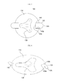
- the sub reflective sheet 100 includes a body portion 110 and a fitting portion 120 .
- An outer circumference of the body portion 110 may be substantially circular when viewed from above.
- a sub opening 130 is formed in the body portion 110 .
- the sub opening 130 provides a space into which an LED chip 300 and lens supports 343 are inserted.
- the sub opening 130 may be formed along the periphery of the space in which the LED chip 330 and the lens supports 343 are disposed.
- the fitting portion 120 is partially separated from the body portion 110 .
- the fitting portion 120 may have a shape like a boss that protrudes outward from a first end 120 a .
- the first end 120 a of the fitting portion 120 is connected to the body portion 110 .
- the fitting portion 120 may be integrally connected to the body portion 110 at the first end 120 a .
- a connecting portion of the fitting portion 120 and the body portion 110 may be located inside the outer circumference of the body portion 110 having circular shape.
- Both sides 120 b of the fitting portion 120 which face each other may be separated from the body portion 110 by cutting portions 140 , respectively.
- Each of the cutting portions 140 may be defined as a gap having a fine width between the fitting portion 120 and the body portion 110 .
- the sides 120 b of the fitting portion 120 may be formed as lines parallel to each other or straight lines heading toward a center of the body portion 110 , but the inventive concept is not limited thereto.
- a second end 120 c of the fitting portion 120 may be curved. The second end 120 c of the fitting portion 120 may protrude outward than the outer circumference of the body portion 110 .
- the fitting portion 120 can move independently in a vertical direction with respect to the body portion 110 . That is, the fitting portion 120 can be bent or folded upward or downward from the body portion 110 . If the fitting portion 120 is placed in the same plane with the body portion 110 (that is, the state that the sub reflective sheet 100 is not fitted to the main reflective sheet 200 ), the sides 120 b of the fitting portion 120 may be adjacent to the body portion 110 .
- the sub reflective sheet 100 may include a plurality of fitting portions 120 .
- two fitting portions 120 are arranged to have a line of symmetry.
- the sub reflective sheet 100 under the optical lens 340 is disposed on the lower housing 310 .
- a diameter or width of the body portion 110 of the sub reflective sheet 100 may be greater than that of the optical lens 340 and that of the main opening 210 of the main reflective sheet 200 .
- the diameter or width of the main opening 210 of the main reflective sheet 200 may be greater than that of the optical lens 340 .
- the main reflective sheet 200 may overlap a periphery of the body portion 110 .
- the periphery of the body portion 110 may be disposed on one surface (e.g., a lower surface) of the main reflective sheet 200 .
- the fitting portions 120 may be disposed on the other surface (e.g., an upper surface) of the main reflective sheet 200 .
- the sub reflective sheet 100 may be fitted into the main opening 210 of the main reflective sheet 200 through the space.
- the movement of the sub reflective sheet 100 relative to the main reflective sheet 200 may be limited. This can prevent or reduce the lifting of the sub reflective sheet 100 or the main reflective sheet 200 , thereby improving the light quality of the backlight assembly 10 and the display quality of the display device 50 .
- the sub reflective sheet 100 is disposed under the optical lens 340 , even if light emitted from the LED chip 300 travels downward, opposite to the optical lens 340 , the sub reflective sheet 100 can effectively reflect the light toward the optical lens 340 . Therefore, the luminance of the backlight assembly 10 can be improved.
- the PCB 320 having the LED chip 330 mounted thereon is placed in the recessed portion 312 of the lower housing 310 .
- the sub reflective sheet 100 is placed on the LED chip 330 .
- the sub reflective sheet 100 is placed such that the LED chip 330 can be exposed through the sub opening 130 of the sub reflective sheet 100 .
- optical lens 340 is installed.
- the lens supports 343 of the optical lens 340 are placed on the lower housing 310 exposed through the sub opening 130 of the sub reflective sheet 100 and then coupled onto the bottom portion 311 of the lower housing 310 by an adhesive or a double-sided tape.
- the main reflective sheet 200 is mounted.
- the optical lens 340 pass through the main opening 210 of the main reflective sheet 200 such that the main reflective sheet 200 is placed over the surface of the lower housing 310 and an upper surface of the sub reflective sheet 100 .
- the fitting portions 120 of the sub reflective sheet 100 are bent upward through the main opening 210 and then bent again toward the upper surface of the main reflective sheet 200 , such that the sub reflective sheet 100 is fitted to the main reflective sheet 200 through the main opening 210 .
- FIG. 7 is a plan view of a sub reflective sheet 101 of a backlight assembly according to other embodiment of the inventive concept.
- the sub reflective sheet 101 according to the current embodiment is different from the sub reflective sheet 100 according to the embodiment of FIG. 5 in that a sub opening 131 is formed to surround the outside of a space in which lens supports are disposed. Since the sub opening 131 is formed wider, a reflective area is relatively reduced. However, since a pattern of the sub opening 131 is formed regardless of the positions of the lens supports, the sub reflective sheet 100 can be assembled easily.
- FIG. 8 is a plan view of a sub reflective sheet of a backlight assembly according to another embodiment of the inventive concept.
- sub openings 132 are formed only in spaces in which an LED chip and lens supports of an optical lens are disposed, and a space other than these spaces serves as a reflective surface of the sub reflective sheet 102 . Accordingly, in the current embodiment, a reflective area is relatively increased, thereby improving luminance.
- FIG. 9 is a plan view of a sub reflective sheet of a backlight assembly according to still another embodiment of the inventive concept.
- the sub reflective sheet 103 according to the current embodiment is different from the sub reflective sheet 100 according to the embodiment of FIG. 5 in that it includes four fitting portions 123 . That is, two fitting portions 123 form a pair, and two pairs of the fitting portions 123 are arranged to have a line of symmetry. The increased number of the fitting portions 123 enables the sub reflective sheet 103 to be coupled more securely to a main reflective sheet 200 .
- a plurality of fitting portions may also be arranged at regular intervals along an outer circumference of a body portion.
- FIG. 10 is a plan view of a sub reflective sheet of a backlight assembly according to still another embodiment of the inventive concept.
- the sub reflective sheet 104 according to the current embodiment is different from the sub reflective sheet 100 according to the embodiment of FIG. 5 in that a second end 124 c of each fitting portion 124 of the sub reflective sheet 104 is not protruded from an outer circumference of a body portion 110 but are formed along the outer circumference of the body portion 110 (that is, a part of a circle).
- the sub reflective sheet 104 can be fitted to a main reflective sheet 200 by placing the body portion 110 of the sub reflective sheet 104 on a lower surface of the main reflective sheet 200 and placing the fitting portions 124 on an upper surface of the main reflective sheet 200 .
- an overlap area between the periphery of the body portion 110 of the sub reflective sheet 104 and the main reflective sheet 200 may be increased relatively.
- FIG. 11 is a plan view of a sub reflective sheet of a backlight assembly according to still another embodiment of the inventive concept.
- the sub reflective sheet 105 according to the current embodiment is different from the sub reflective sheet 100 according to the embodiment of FIG. 5 in that a cutting portion 145 separating each fitting portion 125 from a body portion 110 includes a concave portion whose width increases toward a second end 125 c (toward an outer circumference of the body portion 110 ) and decreases toward a first end 125 a (toward a center of the body portion 110 ).
- the second end 125 c of each fitting portion 125 may be located outside the outer circumference of the body portion 110 .
- each fitting portion 125 Since both sides 125 b of each fitting portion 125 are separated from the body portion 110 by the cutting portions 145 having the concave portions, the fitting portions 125 can move independently in a vertical direction with respect to the body portion 110 . In addition, since the sides 125 b of each fitting portion 125 are separated relatively far away from the body portion 110 , the fitting portions 125 can move more freely. Accordingly, the sub reflective sheet 105 can be fitted to a main reflective sheet more easily in an assembling process.
- FIG. 12 is a plan view of a sub reflective sheet of a backlight assembly according to still another embodiment of the inventive concept.
- the sub reflective sheet 106 according to the current embodiment is different from the sub reflective sheet 105 according to the embodiment of FIG. 11 in that a second end 126 c of each fitting portion 126 of the sub reflective sheet 106 is not protruded from an outer circumference of a body portion 110 .
- the second end 126 c of each fitting portion 126 may be formed along the outer circumference of the body portion 110 . Even if the fitting portions 126 is not protruded from the outer circumference of the body portion 110 , the sub reflective sheet 106 can be fitted to a main reflective sheet as described above in the embodiment of FIG. 10 .
- FIG. 13 is a plan view of a main reflective sheet of a backlight assembly according to still another embodiment of the inventive concept.
- FIG. 14 is a partial layout view illustrating the main reflective sheet of FIG. 13 and a sub reflective sheet coupled to each other.
- FIG. 15 is a cross-sectional view taken along the line XV-XV′ of FIG. 14 .
- fitting portions 212 are formed not in the sub reflective sheet 107 , but in the main reflective sheet 201 .
- the main reflective sheet 201 may include reflective portion, main openings 211 and the fitting portions 212 which protrude from circumferences of the main openings 211 toward the centers of the main opening 211 .
- the fitting portions 212 are separated from a body portion of the main reflective sheet 201 by cutting portions 213 .
- Each fitting portion 212 has a first end connected to the body portion of the main reflective sheet 201 , both sides separated from the body portion of the main reflective sheet 201 , and a second end protruding toward a center of a corresponding main opening 211 .
- the second end of each fitting portion 212 may not protrude from an inner circumferential surface of a corresponding main opening 211 but may be formed along the inner circumference of the corresponding main opening 211 .
- the sub reflective sheet 107 may include a body portion and a sub opening 130 .
- the sub reflective sheet 107 may not have fitting portions.
- An outer circumference of the body portion of the sub reflective sheet 107 may be circular.
- the main reflective sheet 201 is basically placed on a surface (e.g., an upper surface) of the sub reflective sheet 107 , but the fitting portions 212 of the main reflective sheet 201 are placed on the other surface (e.g., a lower surface) of the sub reflective sheet 107 . That is, the sub reflective sheet 107 may be fitted to the main reflective sheet 201 by the fitting portions 212 of the main reflective sheet 201 . Therefore, in the current embodiment, the movement of the sub reflective sheet 107 relative to the main reflective sheet 201 is also limited, and the lifting of the main reflective sheet 201 or the sub reflective sheet 107 can be prevented or reduced.
- both a main reflective sheet and a sub reflective sheet may each include a body portion and fitting portions physically separated from the body portion.
- Embodiments of the inventive concept provide at least one of the following advantages.
Applications Claiming Priority (2)
| Application Number | Priority Date | Filing Date | Title |
|---|---|---|---|
| KR1020140011608A KR102137135B1 (ko) | 2014-01-29 | 2014-01-29 | 백라이트 어셈블리 및 이를 포함하는 표시 장치 |
| KR10-2014-0011608 | 2014-01-29 |
Publications (2)
| Publication Number | Publication Date |
|---|---|
| US20150211715A1 US20150211715A1 (en) | 2015-07-30 |
| US9612474B2 true US9612474B2 (en) | 2017-04-04 |
Family
ID=53678673
Family Applications (1)
| Application Number | Title | Priority Date | Filing Date |
|---|---|---|---|
| US14/273,386 Expired - Fee Related US9612474B2 (en) | 2014-01-29 | 2014-05-08 | Backlight assembly and display device including the same |
Country Status (2)
| Country | Link |
|---|---|
| US (1) | US9612474B2 (ko) |
| KR (1) | KR102137135B1 (ko) |
Cited By (2)
| Publication number | Priority date | Publication date | Assignee | Title |
|---|---|---|---|---|
| US11327362B2 (en) * | 2014-11-14 | 2022-05-10 | Lg Electronics Inc. | Display device |
| US11366355B2 (en) | 2019-10-21 | 2022-06-21 | Samsung Electronics Co., Ltd. | Direct type back light device and display apparatus having the same |
Families Citing this family (8)
| Publication number | Priority date | Publication date | Assignee | Title |
|---|---|---|---|---|
| CN204100138U (zh) * | 2014-09-30 | 2015-01-14 | 京东方科技集团股份有限公司 | 一种反射片、背光模组和显示装置 |
| JP6601146B2 (ja) * | 2015-10-26 | 2019-11-06 | 船井電機株式会社 | 表示装置 |
| US10580346B2 (en) * | 2016-03-30 | 2020-03-03 | Panasonic Intellectual Property Management Co., Ltd. | Display device including a plurality of flexible LED mounting boards |
| KR102565668B1 (ko) * | 2016-10-18 | 2023-08-09 | 엘지디스플레이 주식회사 | 백라이트 유닛 및 이를 포함한 액정표시장치 |
| CN109212826B (zh) * | 2017-06-29 | 2021-07-27 | 中强光电股份有限公司 | 光源模块 |
| CN109613758A (zh) * | 2019-02-02 | 2019-04-12 | 京东方科技集团股份有限公司 | 背光模组和显示装置 |
| WO2021070993A1 (ko) * | 2019-10-11 | 2021-04-15 | 엘지전자 주식회사 | 디스플레이 장치 |
| KR20210109124A (ko) | 2020-02-27 | 2021-09-06 | 주식회사 쉘파스페이스 | 조명장치 |
Citations (21)
| Publication number | Priority date | Publication date | Assignee | Title |
|---|---|---|---|---|
| JP2005092000A (ja) | 2003-09-19 | 2005-04-07 | Kawaguchiko Seimitsu Co Ltd | バックライト付液晶表示装置 |
| US20070189011A1 (en) | 2006-02-14 | 2007-08-16 | Samsung Electronics Co., Ltd. | Light-generating module, backlight assembly and display device having the same, and method thereof |
| JP2011023176A (ja) | 2009-07-14 | 2011-02-03 | Sharp Corp | 照明装置、液晶表示装置及び素子基板の板取り方法 |
| US20110096265A1 (en) | 2009-10-26 | 2011-04-28 | Kenichi Murakoshi | Backlight unit and display device including the same |
| US20110109814A1 (en) * | 2009-11-06 | 2011-05-12 | Sharp Kabushiki Kaisha | Lighting device, and display apparatus providing lighting device |
| JP2011165434A (ja) | 2010-02-08 | 2011-08-25 | Panasonic Corp | 光源、バックライトユニット及び液晶表示装置 |
| US8045091B2 (en) | 2006-12-29 | 2011-10-25 | Lg Innotek Co., Ltd. | Backlight unit and dislay device having the same |
| JP2011248121A (ja) | 2010-05-27 | 2011-12-08 | Panasonic Liquid Crystal Display Co Ltd | 液晶表示装置 |
| US20120086871A1 (en) | 2009-06-15 | 2012-04-12 | Sharp Kabushiki Kaisha | Light emitting module, illuminating device, display device, and television receiver |
| US20120092568A1 (en) | 2009-07-03 | 2012-04-19 | Sharp Kabushiki Kaisha | Lighting device, display device and television receiver |
| US20120099026A1 (en) * | 2009-07-03 | 2012-04-26 | Sharp Kabushiki Kaisha | Light source unit, lighting device, display device and television receiver |
| US20120262631A1 (en) | 2009-12-28 | 2012-10-18 | Sharp Kabushiki Kaisha | Lighting device, display device and television receiver |
| US20130050588A1 (en) * | 2010-06-02 | 2013-02-28 | Kentaro Kamada | Lighting device, display device and television device |
| US20130050589A1 (en) * | 2010-06-02 | 2013-02-28 | Kentaro Kamada | Lighting device, display device and television device |
| JP2013118055A (ja) | 2011-12-01 | 2013-06-13 | Sharp Corp | 照明装置、表示装置、及びテレビ受信装置 |
| JP2013118117A (ja) | 2011-12-05 | 2013-06-13 | Sharp Corp | 照明装置、表示装置、及びテレビ受信装置 |
| US20140061684A1 (en) * | 2012-08-31 | 2014-03-06 | Nichia Corporation | Light-emitting device and method of manufacturing the same |
| US20140098520A1 (en) * | 2009-05-22 | 2014-04-10 | Sharp Kabushiki Kaisha | Light source device and display device |
| US20140185296A1 (en) * | 2012-12-28 | 2014-07-03 | Nichia Corporation | Light emitting device |
| US20140321156A1 (en) * | 2011-11-11 | 2014-10-30 | Sharp Kabushiki Kaisha | Backlight device |
| US20150226400A1 (en) * | 2011-03-25 | 2015-08-13 | Sharp Kabushiki Kaisha | Light-emitting device, illuminating apparatus, and display apparatus |
-
2014
- 2014-01-29 KR KR1020140011608A patent/KR102137135B1/ko active IP Right Grant
- 2014-05-08 US US14/273,386 patent/US9612474B2/en not_active Expired - Fee Related
Patent Citations (21)
| Publication number | Priority date | Publication date | Assignee | Title |
|---|---|---|---|---|
| JP2005092000A (ja) | 2003-09-19 | 2005-04-07 | Kawaguchiko Seimitsu Co Ltd | バックライト付液晶表示装置 |
| US20070189011A1 (en) | 2006-02-14 | 2007-08-16 | Samsung Electronics Co., Ltd. | Light-generating module, backlight assembly and display device having the same, and method thereof |
| US8045091B2 (en) | 2006-12-29 | 2011-10-25 | Lg Innotek Co., Ltd. | Backlight unit and dislay device having the same |
| US20140098520A1 (en) * | 2009-05-22 | 2014-04-10 | Sharp Kabushiki Kaisha | Light source device and display device |
| US20120086871A1 (en) | 2009-06-15 | 2012-04-12 | Sharp Kabushiki Kaisha | Light emitting module, illuminating device, display device, and television receiver |
| US20120092568A1 (en) | 2009-07-03 | 2012-04-19 | Sharp Kabushiki Kaisha | Lighting device, display device and television receiver |
| US20120099026A1 (en) * | 2009-07-03 | 2012-04-26 | Sharp Kabushiki Kaisha | Light source unit, lighting device, display device and television receiver |
| JP2011023176A (ja) | 2009-07-14 | 2011-02-03 | Sharp Corp | 照明装置、液晶表示装置及び素子基板の板取り方法 |
| US20110096265A1 (en) | 2009-10-26 | 2011-04-28 | Kenichi Murakoshi | Backlight unit and display device including the same |
| US20110109814A1 (en) * | 2009-11-06 | 2011-05-12 | Sharp Kabushiki Kaisha | Lighting device, and display apparatus providing lighting device |
| US20120262631A1 (en) | 2009-12-28 | 2012-10-18 | Sharp Kabushiki Kaisha | Lighting device, display device and television receiver |
| JP2011165434A (ja) | 2010-02-08 | 2011-08-25 | Panasonic Corp | 光源、バックライトユニット及び液晶表示装置 |
| JP2011248121A (ja) | 2010-05-27 | 2011-12-08 | Panasonic Liquid Crystal Display Co Ltd | 液晶表示装置 |
| US20130050588A1 (en) * | 2010-06-02 | 2013-02-28 | Kentaro Kamada | Lighting device, display device and television device |
| US20130050589A1 (en) * | 2010-06-02 | 2013-02-28 | Kentaro Kamada | Lighting device, display device and television device |
| US20150226400A1 (en) * | 2011-03-25 | 2015-08-13 | Sharp Kabushiki Kaisha | Light-emitting device, illuminating apparatus, and display apparatus |
| US20140321156A1 (en) * | 2011-11-11 | 2014-10-30 | Sharp Kabushiki Kaisha | Backlight device |
| JP2013118055A (ja) | 2011-12-01 | 2013-06-13 | Sharp Corp | 照明装置、表示装置、及びテレビ受信装置 |
| JP2013118117A (ja) | 2011-12-05 | 2013-06-13 | Sharp Corp | 照明装置、表示装置、及びテレビ受信装置 |
| US20140061684A1 (en) * | 2012-08-31 | 2014-03-06 | Nichia Corporation | Light-emitting device and method of manufacturing the same |
| US20140185296A1 (en) * | 2012-12-28 | 2014-07-03 | Nichia Corporation | Light emitting device |
Cited By (3)
| Publication number | Priority date | Publication date | Assignee | Title |
|---|---|---|---|---|
| US11327362B2 (en) * | 2014-11-14 | 2022-05-10 | Lg Electronics Inc. | Display device |
| US11709395B2 (en) | 2014-11-14 | 2023-07-25 | Lg Electronics Inc. | Display device |
| US11366355B2 (en) | 2019-10-21 | 2022-06-21 | Samsung Electronics Co., Ltd. | Direct type back light device and display apparatus having the same |
Also Published As
| Publication number | Publication date |
|---|---|
| US20150211715A1 (en) | 2015-07-30 |
| KR20150090693A (ko) | 2015-08-06 |
| KR102137135B1 (ko) | 2020-07-27 |
Similar Documents
| Publication | Publication Date | Title |
|---|---|---|
| US9612474B2 (en) | Backlight assembly and display device including the same | |
| KR102203950B1 (ko) | 광원 모듈, 이를 포함하는 백라이트 어셈블리 및 표시 장치 | |
| US20150219940A1 (en) | Curved backlight assembly and curved display device having the same | |
| KR102395088B1 (ko) | 백라이트 유닛 및 이를 포함하는 액정 표시 장치 | |
| US10353132B2 (en) | Display device | |
| KR102105994B1 (ko) | 액정표시장치 및 이의 제조 방법 | |
| KR101818252B1 (ko) | 백라이트 유닛 및 이를 포함하는 액정표시장치 | |
| KR20140106905A (ko) | 액정표시장치 | |
| WO2017094840A1 (ja) | 照明装置、表示装置及びテレビ受信装置 | |
| US8144287B2 (en) | Optical member unit, lighting device for display, display, and television receiver | |
| WO2012165282A1 (ja) | 照明装置、表示装置、及びテレビ受信装置 | |
| US20120314153A1 (en) | Liquid crystal display device | |
| WO2011055635A1 (ja) | 光源ユニット用母材、照明装置、表示装置、及びテレビ受信装置 | |
| KR102159949B1 (ko) | 커브드 표시장치 | |
| KR102166050B1 (ko) | 백라이트 유닛 및 이를 구비한 액정표시장치 | |
| WO2011062023A1 (ja) | 照明装置、表示装置、及びテレビ受信装置 | |
| US9116277B2 (en) | Lighting device, display device, and television receiver | |
| KR102210604B1 (ko) | 백라이트 유닛 및 이를 구비한 액정표시장치 | |
| JP5368586B2 (ja) | 照明装置、表示装置、テレビ受信装置 | |
| JP2013118055A (ja) | 照明装置、表示装置、及びテレビ受信装置 | |
| KR102102703B1 (ko) | Led 패키지, 그 제조 방법, led 패키지를 포함하는 백라이트 유닛 및 액정표시장치 | |
| KR20220075846A (ko) | 표시 장치 | |
| KR102484865B1 (ko) | 표시장치 | |
| KR102234572B1 (ko) | 액정표시장치 | |
| KR102272047B1 (ko) | 액정표시장치 |
Legal Events
| Date | Code | Title | Description |
|---|---|---|---|
| AS | Assignment |
Owner name: SAMSUNG DISPLAY CO., LTD., KOREA, REPUBLIC OF Free format text: ASSIGNMENT OF ASSIGNORS INTEREST;ASSIGNOR:SONG, SI JOON;REEL/FRAME:032853/0900 Effective date: 20140408 |
|
| FEPP | Fee payment procedure |
Free format text: PAYOR NUMBER ASSIGNED (ORIGINAL EVENT CODE: ASPN); ENTITY STATUS OF PATENT OWNER: LARGE ENTITY |
|
| STCF | Information on status: patent grant |
Free format text: PATENTED CASE |
|
| FEPP | Fee payment procedure |
Free format text: MAINTENANCE FEE REMINDER MAILED (ORIGINAL EVENT CODE: REM.); ENTITY STATUS OF PATENT OWNER: LARGE ENTITY |
|
| LAPS | Lapse for failure to pay maintenance fees |
Free format text: PATENT EXPIRED FOR FAILURE TO PAY MAINTENANCE FEES (ORIGINAL EVENT CODE: EXP.); ENTITY STATUS OF PATENT OWNER: LARGE ENTITY |
|
| STCH | Information on status: patent discontinuation |
Free format text: PATENT EXPIRED DUE TO NONPAYMENT OF MAINTENANCE FEES UNDER 37 CFR 1.362 |
|
| FP | Lapsed due to failure to pay maintenance fee |
Effective date: 20210404 |