US9542353B2 - System and method for reducing command scheduling constraints of memory circuits - Google Patents
System and method for reducing command scheduling constraints of memory circuits Download PDFInfo
- Publication number
- US9542353B2 US9542353B2 US11/929,225 US92922507A US9542353B2 US 9542353 B2 US9542353 B2 US 9542353B2 US 92922507 A US92922507 A US 92922507A US 9542353 B2 US9542353 B2 US 9542353B2
- Authority
- US
- United States
- Prior art keywords
- memory circuits
- physical memory
- interface circuit
- circuits
- memory
- Prior art date
- Legal status (The legal status is an assumption and is not a legal conclusion. Google has not performed a legal analysis and makes no representation as to the accuracy of the status listed.)
- Active, expires
Links
Images


Classifications
-
- G—PHYSICS
- G06—COMPUTING; CALCULATING OR COUNTING
- G06F—ELECTRIC DIGITAL DATA PROCESSING
- G06F13/00—Interconnection of, or transfer of information or other signals between, memories, input/output devices or central processing units
- G06F13/38—Information transfer, e.g. on bus
- G06F13/42—Bus transfer protocol, e.g. handshake; Synchronisation
- G06F13/4204—Bus transfer protocol, e.g. handshake; Synchronisation on a parallel bus
- G06F13/4234—Bus transfer protocol, e.g. handshake; Synchronisation on a parallel bus being a memory bus
- G06F13/4243—Bus transfer protocol, e.g. handshake; Synchronisation on a parallel bus being a memory bus with synchronous protocol
-
- G—PHYSICS
- G06—COMPUTING; CALCULATING OR COUNTING
- G06F—ELECTRIC DIGITAL DATA PROCESSING
- G06F13/00—Interconnection of, or transfer of information or other signals between, memories, input/output devices or central processing units
- G06F13/14—Handling requests for interconnection or transfer
- G06F13/20—Handling requests for interconnection or transfer for access to input/output bus
- G06F13/28—Handling requests for interconnection or transfer for access to input/output bus using burst mode transfer, e.g. direct memory access DMA, cycle steal
-
- G—PHYSICS
- G11—INFORMATION STORAGE
- G11C—STATIC STORES
- G11C11/00—Digital stores characterised by the use of particular electric or magnetic storage elements; Storage elements therefor
- G11C11/21—Digital stores characterised by the use of particular electric or magnetic storage elements; Storage elements therefor using electric elements
- G11C11/34—Digital stores characterised by the use of particular electric or magnetic storage elements; Storage elements therefor using electric elements using semiconductor devices
- G11C11/40—Digital stores characterised by the use of particular electric or magnetic storage elements; Storage elements therefor using electric elements using semiconductor devices using transistors
- G11C11/401—Digital stores characterised by the use of particular electric or magnetic storage elements; Storage elements therefor using electric elements using semiconductor devices using transistors forming cells needing refreshing or charge regeneration, i.e. dynamic cells
- G11C11/406—Management or control of the refreshing or charge-regeneration cycles
- G11C11/40618—Refresh operations over multiple banks or interleaving
-
- G—PHYSICS
- G11—INFORMATION STORAGE
- G11C—STATIC STORES
- G11C11/00—Digital stores characterised by the use of particular electric or magnetic storage elements; Storage elements therefor
- G11C11/21—Digital stores characterised by the use of particular electric or magnetic storage elements; Storage elements therefor using electric elements
- G11C11/34—Digital stores characterised by the use of particular electric or magnetic storage elements; Storage elements therefor using electric elements using semiconductor devices
- G11C11/40—Digital stores characterised by the use of particular electric or magnetic storage elements; Storage elements therefor using electric elements using semiconductor devices using transistors
- G11C11/401—Digital stores characterised by the use of particular electric or magnetic storage elements; Storage elements therefor using electric elements using semiconductor devices using transistors forming cells needing refreshing or charge regeneration, i.e. dynamic cells
- G11C11/4063—Auxiliary circuits, e.g. for addressing, decoding, driving, writing, sensing or timing
- G11C11/407—Auxiliary circuits, e.g. for addressing, decoding, driving, writing, sensing or timing for memory cells of the field-effect type
- G11C11/409—Read-write [R-W] circuits
- G11C11/4093—Input/output [I/O] data interface arrangements, e.g. data buffers
-
- Y02B60/1228—
-
- Y02B60/1235—
-
- Y—GENERAL TAGGING OF NEW TECHNOLOGICAL DEVELOPMENTS; GENERAL TAGGING OF CROSS-SECTIONAL TECHNOLOGIES SPANNING OVER SEVERAL SECTIONS OF THE IPC; TECHNICAL SUBJECTS COVERED BY FORMER USPC CROSS-REFERENCE ART COLLECTIONS [XRACs] AND DIGESTS
- Y02—TECHNOLOGIES OR APPLICATIONS FOR MITIGATION OR ADAPTATION AGAINST CLIMATE CHANGE
- Y02D—CLIMATE CHANGE MITIGATION TECHNOLOGIES IN INFORMATION AND COMMUNICATION TECHNOLOGIES [ICT], I.E. INFORMATION AND COMMUNICATION TECHNOLOGIES AIMING AT THE REDUCTION OF THEIR OWN ENERGY USE
- Y02D10/00—Energy efficient computing, e.g. low power processors, power management or thermal management
Definitions
- the present invention relates to memory, and more particularly to command scheduling constraints of memory circuits.
- An interface circuit is capable of communication with a plurality of memory circuits and a system. In use, the interface circuit is operable to interface the memory circuits and the system for reducing command scheduling constraints of the memory circuits.
- FIG. 1 illustrates a system for interfacing memory circuits, in accordance with one embodiment
- FIG. 2 illustrates a method for reducing command scheduling constraints of memory circuits, in accordance with another embodiment.
- FIG. 3 illustrates a method for translating an address associated with a command communicated between a system and memory circuits, in accordance with yet another embodiment.
- FIG. 4 illustrates a block diagram including logical components of a computer platform, in accordance with another embodiment.
- FIG. 5 illustrates a timing diagram showing an intra-device command sequence, intra-device timing constraints, and resulting idle cycles that prevent full use of bandwidth utilization in a DDR3 SDRAM memory system, in accordance with yet another embodiment.
- FIG. 6 illustrates a timing diagram showing an inter-device command sequence, inter-device timing constraints, and resulting idle cycles that prevent full use of bandwidth utilization in a DDR SDRAM, DDR2 SDRAM, or DDR3 SDRAM memory system, in accordance with still yet another embodiment.
- FIG. 7 illustrates a block diagram showing an array of DRAM devices connected to a memory controller, in accordance with another embodiment.
- FIG. 8 illustrates a block diagram showing an interface circuit disposed between an array of DRAM devices and a memory controller, in accordance with yet another embodiment.
- FIG. 9 illustrates a block diagram showing a DDR3 SDRAM interface circuit disposed between an array of DRAM devices and a memory controller, in accordance with another embodiment.
- FIG. 10 illustrates a block diagram showing a burst-merging interface circuit connected to multiple DRAM devices with multiple independent data buses, in accordance with still yet another embodiment.
- FIG. 11 illustrates a timing diagram showing continuous data transfer over multiple commands in a command sequence, in accordance with another embodiment.
- FIG. 12 illustrates a block diagram showing a protocol translation and interface circuit connected to multiple DRAM devices with multiple independent data buses, in accordance with yet another embodiment.
- FIG. 13 illustrates a timing diagram showing the effect when a memory controller issues a column-access command late, in accordance with another embodiment.
- FIG. 14 illustrates a timing diagram showing the effect when a memory controller issues a column-access command early, in accordance with still yet another embodiment.
- FIG. 15 illustrates a representative hardware environment, in accordance with one embodiment.
- FIG. 1 illustrates a system 100 for interfacing memory circuits, in accordance with one embodiment.
- the system 100 includes an interface circuit 104 in communication with a plurality of memory circuits 102 and a system 106 .
- memory circuits 102 may include any circuits capable of serving as memory.
- the memory circuits 102 may include a monolithic memory circuit, a semiconductor die, a chip, a packaged memory circuit, or any other type of tangible memory circuit.
- the memory circuits 102 may take the form of dynamic random access memory (DRAM) circuits.
- DRAM dynamic random access memory
- Such DRAM may take any form including, but not limited to, synchronous DRAM (SDRAM), double data rate synchronous DRAM (DDR SDRAM, DDR2 SDRAM, DDR3 SDRAM, etc.), graphics double data rate DRAM (GDDR, GDDR2, GDDR3, etc.), quad data rate DRAM (QDR DRAM), RAMBUS XDR DRAM (XDR DRAM), fast page mode DRAM (FPM DRAM), video DRAM (VDRAM), extended data out DRAM (EDO DRAM), burst EDO RAM (BBDO DRAM), multibank DRAM (MDRAM), synchronous graphics RAM (SGRAM), and/or any other type of DRAM.
- SDRAM synchronous DRAM
- DDR SDRAM double data rate synchronous DRAM
- DDR2 SDRAM DDR2 SDRAM, DDR3 SDRAM, etc.
- graphics double data rate DRAM GDDR, GDDR2, GDDR3, etc.
- quad data rate DRAM QDR DRAM
- RAMBUS XDR DRAM XDR DRAM
- At least one of the memory circuits 102 may include magnetic random access memory (MRAM), intelligent random access memory (IRAM), distributed network architecture (DNA) memory, window random access memory (WRAM), flash memory (e.g. NAND, NOR, etc.), pseudostatic random access memory (PSRAM), wetware memory, memory based on semiconductor, atomic, molecular, optical, organic, biological, chemical, or nanoscale technology, and/or any other type of volatile or nonvolatile, random or non-random access, serial or parallel access memory circuit.
- MRAM magnetic random access memory
- IRAM intelligent random access memory
- DNA distributed network architecture
- WRAM window random access memory
- PSRAM pseudostatic random access memory
- wetware memory memory based on semiconductor, atomic, molecular, optical, organic, biological, chemical, or nanoscale technology, and/or any other type of volatile or nonvolatile, random or non-random access, serial or parallel access memory circuit.
- the memory circuits 102 may or may not be positioned on at least one dual in-line memory module (DIMM) (not shown).
- the DIMM may include a registered DIMM (R-DIMM), a small outline-DIMM (SO-DIMM), a fully buffered DIMM (FB-DIMM), an unbuffered DIMM (UDIMM), single inline memory module (SIMM), a MiniDIMM, a very low profile (VLP) R-DIMM, etc.
- the memory circuits 102 may or may not be positioned on any type of material forming a substrate, card, module, sheet, fabric, board, carrier or any other type of solid or flexible entity, form, or object.
- the memory circuits 102 may or may not be positioned in or on any desired entity, form, or object for packaging purposes.
- the memory circuits 102 may or may not be organized into ranks. Such ranks may refer to any arrangement of such memory circuits 102 on any of the foregoing entities, forms, objects, etc.
- the system 106 may include any system capable of requesting and/or initiating a process that results in an access of the memory circuits 102 .
- the system 106 may accomplish this utilizing a memory controller (not shown), or any other desired mechanism.
- such system 106 may include a system in the form of a desktop computer, a lap-top computer, a server, a storage system, a networking system, a workstation, a personal digital assistant (PDA), a mobile phone, a television, a computer peripheral (e.g. printer, etc.), a consumer electronics system, a communication system, and/or any other software and/or hardware, for that matter.
- PDA personal digital assistant
- the interface circuit 104 may, in the context of the present description, refer to any circuit capable of interfacing (e.g. communicating, buffering, etc.) with the memory circuits 102 and the system 106 .
- the interface circuit 104 may, in the context of different embodiments, include a circuit capable of directly (e.g. via wire, bus, connector, and/or any other direct communication medium, etc.) and/or indirectly (e.g. via wireless, optical, capacitive, electric field, magnetic field, electromagnetic field, and/or any other indirect communication medium, etc.) communicating with the memory circuits 102 and the system 106 .
- the communication may use a direct connection (e.g.
- point-to-point single-drop bus, multi-drop bus, serial bus, parallel bus, link, and/or any other direct connection, etc.
- indirect connection e.g. through intermediate circuits, intermediate logic, an intermediate bus or busses, and/or any other indirect connection, etc.
- the interface circuit 104 may include one or more circuits, such as a buffer (e.g. buffer chip, etc.), a register (e.g. register chip, etc.), an advanced memory buffer (AMB) (e.g. AMB chip, etc.), a component positioned on at least one DIMM, a memory controller, etc.
- the register may, in various embodiments, include a JEDEC Solid State Technology Association (known as JEDEC) standard register (a JEDEC register), a register with forwarding, storing, and/or buffering capabilities, etc.
- JEDEC JEDEC Solid State Technology Association
- the register chips, buffer chips, and/or any other interface circuit 104 may be intelligent, that is, include logic that is capable of one or more functions such as gathering and/or storing information; inferring, predicting, and/or storing state and/or status; performing logical decisions; and/or performing operations on input signals, etc .
- the interface circuit 104 may optionally be manufactured in monolithic form, packaged form, printed form, and/or any other manufactured form of circuit, for that matter.
- the interface circuit 104 may be positioned on a DIMM.
- a plurality of the aforementioned interface circuit 104 may serve, in combination, to interface the memory circuits 102 and the system 106 .
- one, two, three, four, or more interface circuits 104 may be utilized for such interfacing purposes.
- multiple interface circuits 104 may be relatively configured or connected in any desired manner.
- the interface circuits 104 may be configured or connected in parallel, serially, or in various combinations thereof.
- the multiple interface circuits 104 may use direct connections to each other, indirect connections to each other, or even a combination thereof.
- any number of the interface circuits 104 may be allocated to any number of the memory circuits 102 .
- each of the plurality of interface circuits 104 may be the same or different. Even still, the interface circuits 104 may share the same or similar interface tasks and/or perform different interface tasks.
- any of such parts may be integrated in any desired manner.
- integration may involve simply packaging such parts together (e.g. stacking the parts to form a stack of DRAM circuits, a DRAM stack, a plurality of DRAM stacks, a hardware stack, where a stack may refer to any bundle, collection, or grouping of parts and/or circuits, etc.) and/or integrating them monolithically.
- at least one interface circuit 104 (or portion(s) thereof) may be packaged with at least one of the memory circuits 102 . In this way, the interface circuit 104 and the memory circuits 102 may take the form of a stack, in one embodiment.
- a DRAM stack may or may not include at least one interface circuit 104 (or portion(s) thereof).
- different numbers of the interface circuit 104 (or portion(s) thereof) may be packaged together.
- Such different packaging arrangements, when employed, may optionally improve the utilization of a monolithic silicon implementation, for example.
- the interface circuit 104 may be capable of various functionality, in the context of different optional embodiments.
- the interface circuit 104 may or may not be operable to interface a first number of memory circuits 102 and the system 106 for simulating a second number of memory circuits 105 to the system 106 .
- the second number of memory circuits 105 is shown with a dashed border to indicate that its memory circuits are simulated.
- the first number of memory circuits 102 shall hereafter be referred to, where appropriate for clarification purposes, as the “physical” memory circuits 102 or memory circuits, but are not limited to be so.
- the physical memory circuits 102 may include a single physical memory circuit.
- the at least one simulated memory circuit seen by the system 106 shall hereafter be referred to, where appropriate for clarification purposes, as the at least one “virtual” memory circuit.
- the second number of virtual memory circuits may be more than, equal to, or less than the first number of physical memory circuits 102 .
- the second number of virtual memory circuits may include a single memory circuit. Of course, however, any number of memory circuits may be simulated.
- the term simulated may refer to any simulating, emulating, disguising, transforming, modifying, changing, altering, shaping, converting, etc., which results in at least one aspect of the memory circuits 102 appearing different to the system 106 .
- such aspect may include, for example, a number, a signal, a memory capacity, a timing, a latency, a design parameter, a logical interface, a control system, a property, a behavior, and/or any other aspect, for that matter.
- the simulation may be electrical in nature, logical in nature, protocol in nature, and or performed in any other desired manner. For instance, in the context of electrical simulation, a number of pins, wires, signals, etc. may be simulated. In the context of logical simulation, a particular function or behavior may be simulated. In the context of protocol, a particular protocol (e.g. DDR3, etc) may be simulated. Further, in the context of protocol, the simulation may effect conversion between different protocols (e.g. DDR2 and DDR3) or may effect conversion between different versions of the same protocol (e.g. conversion of 4-4-4 DDR2 to 6-6-6 DDR2).
- FIG. 2 illustrates a method 200 for reducing command scheduling constraints of memory circuits, in accordance with another embodiment.
- the method 200 may be implemented in the context of the system 100 of FIG. 1 .
- the method 200 may be implemented.
- the aforementioned definitions may equally apply to the description below.
- a plurality of memory circuits and a system are interfaced.
- the memory circuits and system may be interfaced utilizing an interface circuit.
- the interface circuit may include, for example, the interface circuit described above with respect to FIG. 1 .
- the interfacing may include facilitating communication between the memory circuits and the system.
- the memory circuits and system may be interfaced in any desired manner,
- command scheduling constraints of the memory circuits are reduced, as shown in operation 204 .
- the command scheduling constraints include any limitations associated with scheduling (and/or issuing) commands with respect to the memory circuits.
- the command scheduling constraints may be defined by manufacturers in their memory device data sheets, by standards organizations such as the JEDEC, etc.
- the command scheduling constraints may include intra-device command scheduling constraints.
- Such intra-device command scheduling constraints may include scheduling constraints within a device.
- the intra-device command scheduling constraints may include a column-to-column delay time (tCCD), row-to-row activation delay time (tRRD), four-bank activation window time (tFAW), write-to-read turn-around time (tWTR), etc.
- the intra-device command-scheduling constraints may be associated with parts (e.g. column, row, bank, etc.) of a device (e.g. memory circuit) that share a resource within the memory circuit.
- a device e.g. memory circuit
- the command scheduling constraints may include inter-device command scheduling constraints.
- inter-device scheduling constraints may include scheduling constraints between memory circuits.
- the inter-device command scheduling constraints may include rank-to-rank data bus turnaround times, on-die-termination (ODT) control switching times, etc.
- ODT on-die-termination
- the inter-device command scheduling constraints may be associated with memory circuits that share a resource (e.g. a data bus, etc.) which provides a connection therebetween (e.g. for communicating, etc.).
- a resource e.g. a data bus, etc.
- FIG. 6 One example of such inter-device command scheduling constraints will be described in more detail below with respect to FIG. 6 during the description of a different embodiment.
- command scheduling restraints may include complete elimination and/or any decrease thereof.
- the command scheduling constraints may be reduced by controlling the manner in which commands are issued to the memory circuits. Such commands may include, for example, row-access commands, column-access commands, etc.
- the commands may optionally be issued to the memory circuits utilizing separate busses associated therewith.
- memory circuits associated with separate busses will be described in more detail below with respect to FIG. 8 during the description of a different embodiment.
- the command scheduling constraints may be reduced by issuing commands to the memory circuits based on simulation of a virtual memory circuit.
- the plurality of physical memory circuits and the system may be interfaced such that that the memory circuits appear to the system as a virtual memory circuit.
- Such simulated virtual memory circuit may optionally include the virtual memory circuit described above with respect, to FIG. 1 .
- the virtual memory circuit may have less command scheduling constraints than the physical memory circuits.
- the physical memory circuits may appear as a group of one or more virtual memory circuits that are free from command scheduling constraints.
- the command scheduling constraints may be reduced by issuing commands directed to a single virtual memory circuit, to a plurality of different physical memory circuits. In this way, idle data-bus cycles may optionally be eliminated and memory system bandwidth may be increased.
- the interface circuit may be utilized to eliminate, at least in part, inter-device and/or intra-device command scheduling constraints of memory circuits.
- reduction of the command scheduling constraints of the memory circuits may result in increased command issue rates. For example, a greater amount of commands may be issued to the memory circuits by reducing limitations associated with the command scheduling constraints. More information regarding increasing command issue rates by reducing command scheduling constraints will be described with respect to FIG. 11 during the description of a different embodiment.
- FIG. 3 illustrates a method 300 for translating an address associated with a command communicated between a system and memory circuits, in accordance with yet another embodiment.
- the method 300 may be carried out in context of the architecture and environment of FIGS. 1 and/or 2 .
- the method 300 may be carried out in any desired environment.
- the aforementioned definitions may equally apply to the description below.
- a plurality of memory circuits and a system are interfaced.
- the memory circuits and system may be interfaced utilizing an interface circuit, such as that described above with respect to FIG. 1 , for example.
- the interfacing may include facilitating communication between the memory circuits and the system.
- the memory circuits and system may be interfaced in any desired manner.
- an address associated with a command communicated between the system and the memory circuits is translated, as shown in operation 304 .
- Such command may include, for example, a row-access command, a column-access command, and/or any other command capable of being communicated between the system and the memory circuits.
- the translation may be transparent to the system. In this way, the system may issue a command to the memory circuits, and such command may be translated without knowledge and/or input by the system. Of course, embodiments are contemplated where such transparency is non-existent, at least in part.
- the address may be translated in any desired manner.
- the translation of the address may include shifting the address.
- the address may be translated by mapping the address.
- the memory circuits may include physical memory circuits and the interface circuit may simulate at least one virtual memory circuit.
- the virtual memory circuit may optionally have a different (e.g. greater, etc.) number of row addresses associated therewith than the physical memory circuits.
- the translation may be performed as a function of the difference in the number of row addresses.
- the translation may translate the address to reflect the number of row addresses of the virtual memory circuit.
- the translation may optionally translate the address as a function of a column address and a row address.
- the translation may be performed as a function of an expected arrival time of a column-access command.
- the translation may ensure that a column-access command addresses an open bank.
- the interface circuit may be operable to delay the command communicated between the system and the memory circuits. To this end, the translation may result in sub-row activation of the memory circuits.
- address mapping may use shifting of an address from one command to another to allow the use of memory circuits with smaller rows to emulate a larger memory circuit with larger rows.
- sub-row activation may be provided. Such sub-row activation may also reduce power consumption and may optionally further improve performance, in various embodiments.
- memory storage cells of DRAM devices may be arranged into multiple banks, each bank having multiple rows, and each row having multiple columns.
- the memory storage capacity of the DRAM device may be equal to the number of banks times the number of rows per bank times the number of column per row times the number of storage bits per column.
- commodity DRAM devices e.g.
- the number of banks per device may be determined by a standards-forming committee, such as the Joint Electron Device Engineering Council (JEDEC).
- JEDEC Joint Electron Device Engineering Council
- JEDEC standards require that a 1 gigabyte (Gb) DDR2 or DDR3 SDRAM device with a four-bit wide data bus have eight banks per device, 8192 rows per bank, 2048 columns per row, and four bits per column.
- a 2 Gb device with a four-bit wide data bus has eight banks per device, 16384 rows per bank, 2048 columns per row, and four bits per column.
- a 4 Gb device with a four-bit wide data bus has eight banks per device, 32768 rows per bank, 2048 columns per row, and four bits per column.
- the row size is constant, and the number of rows doubles with each doubling of device capacity.
- a 2 Gb or a 4 Gb device may be simulated, as described above, by using multiple 1 Gb and 2 Gb devices, and by directly translating row-activation commands to row-activation commands and column-access commands to column-access commands.
- this emulation may be possible because the 1 Gb, 2 Gb, and 4 Gb devices have the same row size.
- FIG. 4 illustrates a block diagram including logical components of a computer platform 400 , in accordance with another embodiment.
- the computer platform 400 may be implemented in context of the architecture and environment of FIGS. 1-3 .
- the computer platform 400 may be implemented in any desired environment.
- the aforementioned definitions may equally apply to the description below.
- the computer platform 400 includes a system 420 .
- the system 420 includes a memory interface 421 , logic for retrieval and storage of external memory attribute expectations 422 , memory interaction attributes 423 , a data processing engine 424 , and various mechanisms to facilitate a user interface 425 .
- the computer platform 400 may be comprised of wholly separate components, namely a system 420 (e.g. a motherboard, etc.), and memory circuits 410 (e.g. physical memory circuits, etc.).
- the computer platform 400 may optionally include memory circuits 410 connected directly to the system 420 by way of one or more sockets.
- the memory circuits 410 may be designed to the specifics of various standards, including for example, a standard defining the memory circuits 410 to be JEDEC-compliant semiconductor memory (e.g. DRAM, SDRAM, DDR2, DDR3, etc.).
- a standard defining the memory circuits 410 to be JEDEC-compliant semiconductor memory e.g. DRAM, SDRAM, DDR2, DDR3, etc.
- the specifics of such standards may address physical interconnection and logical capabilities of the memory circuits 410 .
- the system 420 may include a system BIOS program (not shown) capable of interrogating the physical memory circuits 410 (e.g. DIMMs) to retrieve and store memory attributes 422 , 423 .
- various types of external memory circuits 410 including for example JEDEC-compliant DIMMs, may include an EEPROM device known as a serial presence detect (SPD) where the DIMM memory attributes are stored.
- SPD serial presence detect
- the computer platform 400 may include one or more interface circuits 470 electrically disposed between the system 420 and the physical memory circuits 410 .
- the interface circuit 470 may include several system-facing interfaces (e.g. a system address signal interface 471 , a system control signal interface 472 , a system clock signal interlace 473 , a system data signal interlace 474 , etc.).
- the interface circuit 470 may include several memory-facing interlaces (e.g. a memory address signal interface 475 , a memory control signal interface 476 , a memory clock signal interface 477 , a memory data signal interface 478 , etc.).
- the interface circuit 470 may include emulation logic 480 .
- the emulation logic 480 may be operable to receive and optionally store electrical signals (e.g. logic levels, commands, signals, protocol sequences, communications, etc.) from or through the system-facing interlaces, and may further be operable to process such electrical signals.
- the emulation logic 480 may respond to signals from system-facing interfaces by responding back to the system 420 and presenting signals to the system 420 , and may also process the signals with other information previously stored.
- the emulation logic 480 may present signals to the physical memory circuits 410 .
- the emulation logic 480 may perform any of the aforementioned functions in any order.
- the emulation logic 480 may be operable to adopt a personality, where such personality is capable of defining the physical memory circuit attributes.
- the personality may be effected via any combination of bonding options, strapping, programmable strapping, the wiring between the interface circuit 470 and the physical memory circuits 410 .
- the personality may be effected via actual physical attributes (e.g. value of mode register, value of extended mode register) of the physical memory circuits 410 connected to the interface circuit 470 as determined when the interface circuit 470 and physical memory circuits 410 are powered up.
- FIG. 5 illustrates a timing diagram 500 showing an intra-device command sequence, intra-device timing constraints, and resulting idle cycles that prevent full use of bandwidth utilization in a DDR3 SDRAM memory system, in accordance with yet another embodiment.
- the timing diagram 500 may be associated with the architecture and environment of FIGS. 1-4 .
- the timing diagram 500 may be associated with any desired environment. Further, the aforementioned definitions may equally apply to the description below.
- the timing diagram 500 illustrates command cycles, timing constraints and idle cycles of memory.
- any two row-access commands directed to a single DRAM device may not necessarily be scheduled closer than tRRD.
- at most four row-access commands may be scheduled within tFAW to a single DRAM device.
- consecutive column-read access commands and consecutive column-write access commands may not necessarily be scheduled to a given DRAM device any closer than tCCD, where tCCD equals four cycles (eight half-cycles of data) in DDR3 DRAM devices.
- row-access and/or row-activation commands are shown as ACT.
- column-access commands are shown as READ or WRITE.
- the tCCD constraint may prevent column accesses from being scheduled consecutively.
- the constraints 510 , 520 imposed on the DRAM commands sent to a given DRAM device may restrict the command rate, resulting in idle cycles or bubbles 530 on the data bus, therefore reducing the bandwidth.
- consecutive column-access commands sent to different DRAM devices on the same data bus may not necessarily be scheduled any closer than a period that is the sum of the data burst duration plus additional idle cycles due to rank-to-rank data bus turn-around times.
- two DRAM devices on the same data bus may represent two bus masters.
- at least one idle cycle on the bus may be needed for one bus master to complete delivery of data to the memory controller and release control of the shared data bus, such that another bus master may gain control of the data bus and begin to send data.
- FIG. 6 illustrates a timing diagram 600 showing inter-device command sequence, inter-device timing constraints, and resulting idle cycles that prevent full use of bandwidth utilization in a DDR SDRAM, DDR2 SDRAM, or DDR3 SDRAM memory system, in accordance with still yet another embodiment.
- the timing diagram 600 may be associated with the architecture and environment of FIGS. 1-4 .
- the timing diagram 600 may be associated with any desired environment. Further, the aforementioned definitions may equally apply to the description below.
- the timing diagram 600 illustrates commands issued to different devices that are free from constraints such as tRRD and tCCD which would otherwise be imposed on commands issue to the same device.
- the data bus hand-off from one device to another device requires at least one idle data-bus cycle 610 on the data bus.
- the timing diagram 600 illustrates a limitation preventing full use of bandwidth utilization in a DDR3 SDRAM memory system.
- the command-scheduling constraints there may be no available command sequence that allows full bandwidth utilization in a DDR3 SDRAM memory system, which also uses bursts shorter than tCCD.
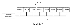
- FIG. 7 illustrates a block diagram 700 showing an array of DRAM devices connected to a memory controller, in accordance with another embodiment.
- the block diagram 700 may be associated with the architecture and environment of FIGS. 1-6 .
- the block diagram 700 may be associated with any desired environment. Further, the aforementioned definitions may equally apply to the description below.
- commands from the memory controller that are directed to the DRAM devices may be issued with respect to command scheduling constraints (e.g. tRRD, tCCD, tFAW, tWTR, etc.).
- command scheduling constraints e.g. tRRD, tCCD, tFAW, tWTR, etc.
- FIG. 8 illustrates a block diagram 800 showing an interface circuit disposed between an array of DRAM devices and a memory controller, in accordance with yet another embodiment.
- the block diagram 800 may be associated with the architecture and environment of FIGS. 1-6 .
- the block diagram 800 may be associated with any desired environment. Further, the aforementioned definitions may equally apply to the description below.
- an interface circuit 810 provides a DRAM interface to the memory controller 820 , and directs commands to independent DRAM devices 830 .
- the memory devices 830 may each be associated with a different data bus 840 , thus preventing inter-device constraints.
- individual and independent memory devices 830 may be used to emulate part, of a virtual memory device (e.g. column, row, bank, etc.). Accordingly, intra-device constraints may also be prevented.
- the memory devices 830 connected to the interface circuit 810 may appear to the memory controller 820 as a group of one or more memory devices 830 that are free from command-scheduling constraints.
- N physical DRAM devices may be used to emulate M logical DRAM devices through the use of the interlace circuit.
- the interface circuit may accept a command stream from a memory controller directed toward the M logical devices.
- the interface circuit may also translate the commands to the N physical devices that are connected to the interface circuit via P independent data paths.
- the command translation may include, for example, routing the correct command directed to one of the M logical devices to the correct device (i.e. one of the N physical devices).
- the P data paths connected to the N physical devices may optionally allow the interface circuit to guarantee that commands may be executed in parallel and independently, thus preventing command-scheduling constraints associated with the N physical devices. In this way the interface circuit may eliminate idle data-bus cycles or bubbles that would otherwise be present due to inter-device and intra-device command-scheduling constraints.
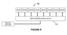
- FIG. 9 illustrates a block diagram 900 showing a DDR3 SDRAM interface circuit disposed between an array of DRAM devices and a memory controller, in accordance with another embodiment.
- the block diagram 900 may be associated with the architecture and environment of FIGS. 1-8 .
- the block diagram 900 may be associated with any desired environment. Further, the aforementioned definitions may equally apply to the description below.
- a DDR3 SDRAM interface circuit 910 eliminates idle data-bus cycles due to inter-device and intra-device scheduling constraints.
- the DDR3 SDRAM interface circuit 910 may include a command translation circuit of an interface circuit that connects multiple DDR3 SDRAM devices with multiple independent data buses.
- the DDR3 SDRAM interface circuit 910 may include command-and-control and address components capable of intercepting signals between the physical memory circuits and the system.
- the command-and-control and address components may allow for burst merging, as described below with respect to FIG. 10 .
- FIG. 10 illustrates a block diagram 1000 showing a burst-merging interface circuit connected to multiple DRAM devices with multiple independent data buses, in accordance with still yet another embodiment.
- the block diagram 1000 may be associated with the architecture and environment of FIGS. 1-9 .
- the block diagram 1000 may be associated with any desired environment. Further, the aforementioned definitions may equally apply to the description below.
- a burst-merging interface circuit 1010 may include a data component of an interface circuit that connects multiple DRAM devices 1030 with multiple independent data buses 1040 .
- the burst-merging interface circuit 1010 may merge multiple burst commands received within a time period.
- eight DRAM devices 1030 may be connected via eight independent data paths to the burst-merging interface circuit 1010 .
- the burst-merging interface circuit 1010 may utilize a single data path to the memory controller 1020 . It should be noted that while eight DRAM devices 1030 are shown herein, in other embodiments, 16, 24, 32, etc. devices may be connected to the eight independent data paths. In yet another embodiment, there may be two, four, eight, 16 or more independent data paths associated with the DRAM devices 1030 .
- the burst-merging interface circuit 1010 may provide a single electrical interface to the memory controller 1020 , therefore eliminating inter-device constraints (e.g. rank-to-rank turnaround time, etc.).
- the memory controller 1020 may be aware that it is indirectly controlling the DRAM devices 1030 through the burst-merging interface circuit 1010 , and that no bus turnaround time is needed.
- the burst-merging interface circuit 1010 may use the DRAM devices 1030 to emulate M logical devices.
- the burst-merging interface circuit 1010 may further translate row-activation commands and column-access commands to one of the DRAM devices 1030 in order to ensure that intra-device constraints (e.g.
- each individual DRAM device 1030 tRRD, tCCD, tFAW and tWTR etc.
- tRRD tRRD
- tCCD tCCD
- tFAW tWTR
- FIG. 11 illustrates a timing diagram 1100 showing continuous data transfer over multiple commands in a command sequence, in accordance with another embodiment.
- the timing diagram 1100 may be associated with the architecture and environment of FIGS. 1-10 .
- the timing diagram 1100 may be associated with any desired environment. Further, the aforementioned definitions may equally apply to the description below.
- an interface circuit associated with the burst-merging interface circuit may present an industry-standard DRAM interface to a memory controller as one or more DRAM devices that are free of command-scheduling constraints. Further, the interface circuits may allow the DRAM devices to be emulated as being free from command-scheduling constraints without necessarily changing the electrical interface or the command set of the DRAM memory system. It should be noted that the interface circuits described herein may include any type of memory system (e.g. DDR2, DDR3, etc.).
- FIG. 12 illustrates a block diagram 1200 showing a protocol translation and interface circuit connected to multiple DRAM devices with multiple independent data buses, in accordance with yet another embodiment.
- the block diagram 1200 may be associated with the architecture and environment of FIGS. 1-11 .
- the block diagram 1200 may be associated with any desired environment. Further, the aforementioned definitions may equally apply to the description below.
- a protocol translation and interface circuit 1210 may perform protocol translation and/or manipulation functions, and may also act as an interface circuit.
- the protocol translation and interlace circuit 1210 may be included within an interface circuit connecting a memory controller with multiple memory devices.
- the protocol translation and interface circuit 1210 may delay row-activation commands and/or column-access commands.
- the protocol translation and interface circuit 1210 may also transparently perform different kinds of address mapping schemes that depend on the expected arrival time of the column-access command.
- the column-access command may be sent by the memory controller at the normal time (i.e. late arrival, as compared to a scheme where the column-access command is early).
- the column-access command may be sent by the memory controller before the row-access command is required (i.e. early arrival) at the DRAM device interface.
- the early arriving column-access command may be referred to as the Posted-CAS command.
- part of a row may be activated as needed, therefore providing sub-row activation.
- lower power may also be provided.
- the protocol translation and interface circuit 1210 may include eight DRAM devices to be connected thereto via eight independent data paths to.
- the protocol translation and interface circuit 1210 may emulate a single 8 Gb DRAM device with eight 1 Gb DRAM devices.
- the memory controller may therefore expect to see eight banks, 32768 rows per bank, 4096 columns per row, and four bits per column.
- the memory controller issues a row-activation command, it may expect that 4096 columns are ready for a column-access command that follows, whereas the 1 Gb devices may only have 2048 columns per row.
- the same issue of differing row sizes may arise when 2 Gb devices are used to emulate a 16 Gb DRAM device or 4 Gb devices are used to emulate a 32 Gb device, etc.
- the protocol translation and interface circuit 1210 may calculate and issue the appropriate number of row-activation commands to prepare for a subsequent column-access command that may access any portion of the larger row.
- the protocol translation and interlace circuit 1210 maybe configured with different behaviors, depending on the specific condition.
- the memory controller may not issue early column-access commands.
- the protocol translation and interface circuit 1210 may activate multiple, smaller rows to match the size of the larger row in the higher capacity logical DRAM device.
- the protocol translation and interface circuit 1210 may present a single data path to the memory controller, as shown.
- the protocol translation and interface circuit 1210 may present itself as a single DRAM device with a single electrical interface to the memory controller.
- the memory controller may expect that the logical 8 Gb DRAM device will take over 300 ns to perform a refresh command.
- the protocol translation and interface circuit 1210 may also Intelligently schedule the refresh commands.
- the protocol translation and interface circuit 1210 may separately schedule refresh commands to the 1 Gb DRAM devices, with each refresh command taking 100 ns.
- the memory controller may expect that the logical device may take a relatively long period to perform a refresh command.
- the protocol translation and interface circuit 1210 may separately schedule refresh commands to each of the physical DRAM devices.
- the refresh of the larger logical DRAM device may take a relatively smaller period of time as compared with a refresh of a physical DRAM device of the same size.
- DDR3 memory systems may potentially require calibration sequences to ensure that the high speed data I/O circuits are periodically calibrated against thermal-variances induced timing drifts.
- the staggered refresh commands may also optionally guarantee I/O quiet time required to separately calibrate each of the independent physical DRAM devices.
- a protocol translation and interlace circuit 1210 may allow for the staggering of refresh times of logical DRAM devices.
- DDR3 devices may optionally require different levels of zero quotient (ZQ) calibration sequences, and the calibration sequences may require guaranteed system quiet time, but may be power intensive, and may require that other I/O in the system are not also switching at the same time.
- ZQ zero quotient
- refresh commands in a higher capacity logical DRAM device may be emulated by staggering refresh commands to different lower capacity physical DRAM devices.
- the staggering of the refresh commands may optionally provide a guaranteed I/O quiet time that may be required to separately calibrate each of the independent physical DRAM: devices.
- FIG. 13 illustrates a timing diagram 1300 showing the effect when a memory controller issues a column-access command late, in accordance with another embodiment.
- the timing diagram 1300 may be associated with the architecture and environment of FIGS. 1-12 .
- the timing diagram 1300 may be associated with any desired environment. Further, the aforementioned definitions may equally apply to the description below.
- the interface circuit may send multiple row-access commands to multiple DRAM devices to guarantee that the subsequent column access will hit an open bank.
- the physical device may have a 1 kilobyte (kb) row size and the logical device may have a 2 kb row size.
- the interface circuit may activate two 1 kb rows in two different physical devices (since two rows may not be activated in the same device within a span of tRRD).
- the physical device may have a 1 kb row size and the logical device may have a 4 kb row size. In this case, four 1 kb rows may be opened to prepare for the arrival of a column-access command that may be targeted to any part of the 4 kb row.
- the memory controller may issue column-access commands early.
- the interface circuit may do this in any desired manner, including for example, using the additive latency property of DDR2 and DDR3 devices.
- the interface circuit may also activate one specific row in one specific DRAM device. This may allow sub-row activation for the higher capacity logical DRAM device.
- FIG. 14 illustrates a timing diagram 1400 showing the effect when a memory controller issues a column-access command early, in accordance with still yet another embodiment.
- the timing diagram 1400 may be associated with the architecture and environment of FIGS. 1-13 .
- the timing diagram 1400 may be associated with any desired environment. Further, the aforementioned definitions may equally apply to the description below.
- a memory controller may issue a column-access command early, i.e. before the row-activation command is to be issued to a DRAM device.
- an interface circuit may take a portion of the column address, combine it with the row address and form a sub-row address. To this end, the interface circuit may activate the row that is targeted by the column-access command.
- the early column-access command may allow the interface circuit to activate a single 1 kb row.
- the interface circuit can thus implement sub-row activation for a logical device with a larger row size than the physical devices without necessarily the use of additional pins or special commands.
- FIG. 15 illustrates a representative hardware environment 1500 , in accordance with one embodiment.
- the hardware environment 1500 may be implemented in the context of FIGS. 1-14 .
- the hardware environment 1500 may constitute an exemplary system.
- the hardware environment 1500 may include a computer system. As shown, the hardware environment 1500 includes at least one central processor 1501 which is connected to a communication bus 1502 . The hardware environment 1500 also includes main memory 1504 .
- the main memory 1504 may include, for example random access memory (RAM) and/or any other desired type of memory. Further, in various embodiments, the main memory 1504 may include memory circuits, interface circuits, etc.
- the hardware environment 1500 also includes a graphics processor 1506 and a display 1508 .
- the hardware environment 1500 may also include a secondary storage 1510 .
- the secondary storage 1510 includes, for example, a hard disk drive and/or a removable storage drive, representing a floppy disk drive, a magnetic tape drive, a compact disk drive, etc.
- the removable storage drive reads from and/or writes to a removable storage unit in a well known manner.
- Computer programs, or computer control logic algorithms may be stored in the main memory 1504 and/or the secondary storage 1510 . Such computer programs, when executed, enable the computer system 1500 to perform various functions. Memory 1504 , storage 1510 and/or any other storage are possible examples of computer-readable media.
Abstract
Description
Claims (14)
Priority Applications (1)
| Application Number | Priority Date | Filing Date | Title |
|---|---|---|---|
| US11/929,225 US9542353B2 (en) | 2006-02-09 | 2007-10-30 | System and method for reducing command scheduling constraints of memory circuits |
Applications Claiming Priority (7)
| Application Number | Priority Date | Filing Date | Title |
|---|---|---|---|
| US77241406P | 2006-02-09 | 2006-02-09 | |
| US11/461,437 US8077535B2 (en) | 2006-07-31 | 2006-07-31 | Memory refresh apparatus and method |
| US86562406P | 2006-11-13 | 2006-11-13 | |
| US11/702,981 US8089795B2 (en) | 2006-02-09 | 2007-02-05 | Memory module with memory stack and interface with enhanced capabilities |
| US11/702,960 US20080126690A1 (en) | 2006-02-09 | 2007-02-05 | Memory module with memory stack |
| US11/672,921 US9542352B2 (en) | 2006-02-09 | 2007-02-08 | System and method for reducing command scheduling constraints of memory circuits |
| US11/929,225 US9542353B2 (en) | 2006-02-09 | 2007-10-30 | System and method for reducing command scheduling constraints of memory circuits |
Related Parent Applications (1)
| Application Number | Title | Priority Date | Filing Date |
|---|---|---|---|
| US11/672,921 Continuation US9542352B2 (en) | 2005-06-24 | 2007-02-08 | System and method for reducing command scheduling constraints of memory circuits |
Publications (2)
| Publication Number | Publication Date |
|---|---|
| US20080120443A1 US20080120443A1 (en) | 2008-05-22 |
| US9542353B2 true US9542353B2 (en) | 2017-01-10 |
Family
ID=46045591
Family Applications (3)
| Application Number | Title | Priority Date | Filing Date |
|---|---|---|---|
| US11/672,921 Active 2030-01-06 US9542352B2 (en) | 2005-06-24 | 2007-02-08 | System and method for reducing command scheduling constraints of memory circuits |
| US11/929,261 Abandoned US20080109595A1 (en) | 2006-02-09 | 2007-10-30 | System and method for reducing command scheduling constraints of memory circuits |
| US11/929,225 Active 2028-12-24 US9542353B2 (en) | 2006-02-09 | 2007-10-30 | System and method for reducing command scheduling constraints of memory circuits |
Family Applications Before (2)
| Application Number | Title | Priority Date | Filing Date |
|---|---|---|---|
| US11/672,921 Active 2030-01-06 US9542352B2 (en) | 2005-06-24 | 2007-02-08 | System and method for reducing command scheduling constraints of memory circuits |
| US11/929,261 Abandoned US20080109595A1 (en) | 2006-02-09 | 2007-10-30 | System and method for reducing command scheduling constraints of memory circuits |
Country Status (1)
| Country | Link |
|---|---|
| US (3) | US9542352B2 (en) |
Cited By (3)
| Publication number | Priority date | Publication date | Assignee | Title |
|---|---|---|---|---|
| US10572168B2 (en) | 2017-11-16 | 2020-02-25 | International Business Machines Corporation | DRAM bank activation management |
| TWI818436B (en) * | 2021-09-22 | 2023-10-11 | 日商鎧俠股份有限公司 | memory system |
| US11893239B2 (en) | 2017-09-14 | 2024-02-06 | Samsung Electronics Co., Ltd. | Quasi-synchronous protocol for large bandwidth memory systems |
Families Citing this family (68)
| Publication number | Priority date | Publication date | Assignee | Title |
|---|---|---|---|---|
| US8060774B2 (en) | 2005-06-24 | 2011-11-15 | Google Inc. | Memory systems and memory modules |
| US7386656B2 (en) | 2006-07-31 | 2008-06-10 | Metaram, Inc. | Interface circuit system and method for performing power management operations in conjunction with only a portion of a memory circuit |
| US8090897B2 (en) | 2006-07-31 | 2012-01-03 | Google Inc. | System and method for simulating an aspect of a memory circuit |
| US8089795B2 (en) | 2006-02-09 | 2012-01-03 | Google Inc. | Memory module with memory stack and interface with enhanced capabilities |
| US20080028136A1 (en) | 2006-07-31 | 2008-01-31 | Schakel Keith R | Method and apparatus for refresh management of memory modules |
| US7515453B2 (en) | 2005-06-24 | 2009-04-07 | Metaram, Inc. | Integrated memory core and memory interface circuit |
| US8397013B1 (en) | 2006-10-05 | 2013-03-12 | Google Inc. | Hybrid memory module |
| US8335894B1 (en) | 2008-07-25 | 2012-12-18 | Google Inc. | Configurable memory system with interface circuit |
| US8081474B1 (en) | 2007-12-18 | 2011-12-20 | Google Inc. | Embossed heat spreader |
| US9507739B2 (en) | 2005-06-24 | 2016-11-29 | Google Inc. | Configurable memory circuit system and method |
| US8438328B2 (en) | 2008-02-21 | 2013-05-07 | Google Inc. | Emulation of abstracted DIMMs using abstracted DRAMs |
| US7609567B2 (en) | 2005-06-24 | 2009-10-27 | Metaram, Inc. | System and method for simulating an aspect of a memory circuit |
| US9542352B2 (en) | 2006-02-09 | 2017-01-10 | Google Inc. | System and method for reducing command scheduling constraints of memory circuits |
| US8327104B2 (en) | 2006-07-31 | 2012-12-04 | Google Inc. | Adjusting the timing of signals associated with a memory system |
| US10013371B2 (en) | 2005-06-24 | 2018-07-03 | Google Llc | Configurable memory circuit system and method |
| US9171585B2 (en) | 2005-06-24 | 2015-10-27 | Google Inc. | Configurable memory circuit system and method |
| US8796830B1 (en) | 2006-09-01 | 2014-08-05 | Google Inc. | Stackable low-profile lead frame package |
| US20080082763A1 (en) | 2006-10-02 | 2008-04-03 | Metaram, Inc. | Apparatus and method for power management of memory circuits by a system or component thereof |
| US8359187B2 (en) | 2005-06-24 | 2013-01-22 | Google Inc. | Simulating a different number of memory circuit devices |
| US8244971B2 (en) | 2006-07-31 | 2012-08-14 | Google Inc. | Memory circuit system and method |
| US8111566B1 (en) | 2007-11-16 | 2012-02-07 | Google, Inc. | Optimal channel design for memory devices for providing a high-speed memory interface |
| US8041881B2 (en) | 2006-07-31 | 2011-10-18 | Google Inc. | Memory device with emulated characteristics |
| US8077535B2 (en) | 2006-07-31 | 2011-12-13 | Google Inc. | Memory refresh apparatus and method |
| US8055833B2 (en) | 2006-10-05 | 2011-11-08 | Google Inc. | System and method for increasing capacity, performance, and flexibility of flash storage |
| US8130560B1 (en) | 2006-11-13 | 2012-03-06 | Google Inc. | Multi-rank partial width memory modules |
| US8386722B1 (en) | 2008-06-23 | 2013-02-26 | Google Inc. | Stacked DIMM memory interface |
| US7379316B2 (en) | 2005-09-02 | 2008-05-27 | Metaram, Inc. | Methods and apparatus of stacking DRAMs |
| US9632929B2 (en) | 2006-02-09 | 2017-04-25 | Google Inc. | Translating an address associated with a command communicated between a system and memory circuits |
| US7724589B2 (en) | 2006-07-31 | 2010-05-25 | Google Inc. | System and method for delaying a signal communicated from a system to at least one of a plurality of memory circuits |
| US8272781B2 (en) * | 2006-08-01 | 2012-09-25 | Intel Corporation | Dynamic power control of a memory device thermal sensor |
| US20080183916A1 (en) * | 2007-01-30 | 2008-07-31 | Mark David Bellows | Using Extreme Data Rate Memory Commands to Scrub and Refresh Double Data Rate Memory |
| US8209479B2 (en) | 2007-07-18 | 2012-06-26 | Google Inc. | Memory circuit system and method |
| US8080874B1 (en) | 2007-09-14 | 2011-12-20 | Google Inc. | Providing additional space between an integrated circuit and a circuit board for positioning a component therebetween |
| TWI359426B (en) * | 2007-09-17 | 2012-03-01 | Asustek Comp Inc | Method for recording parameter of memory and metho |
| US8154901B1 (en) | 2008-04-14 | 2012-04-10 | Netlist, Inc. | Circuit providing load isolation and noise reduction |
| US8001434B1 (en) | 2008-04-14 | 2011-08-16 | Netlist, Inc. | Memory board with self-testing capability |
| US20100005218A1 (en) * | 2008-07-01 | 2010-01-07 | International Business Machines Corporation | Enhanced cascade interconnected memory system |
| US20100005220A1 (en) * | 2008-07-01 | 2010-01-07 | International Business Machines Corporation | 276-pin buffered memory module with enhanced memory system interconnect and features |
| US20100005212A1 (en) * | 2008-07-01 | 2010-01-07 | International Business Machines Corporation | Providing a variable frame format protocol in a cascade interconnected memory system |
| US20100005206A1 (en) * | 2008-07-01 | 2010-01-07 | International Business Machines Corporation | Automatic read data flow control in a cascade interconnect memory system |
| US7717752B2 (en) * | 2008-07-01 | 2010-05-18 | International Business Machines Corporation | 276-pin buffered memory module with enhanced memory system interconnect and features |
| US20100005214A1 (en) * | 2008-07-01 | 2010-01-07 | International Business Machines Corporation | Enhancing bus efficiency in a memory system |
| US20100005219A1 (en) * | 2008-07-01 | 2010-01-07 | International Business Machines Corporation | 276-pin buffered memory module with enhanced memory system interconnect and features |
| US8261174B2 (en) * | 2009-01-13 | 2012-09-04 | International Business Machines Corporation | Protecting and migrating memory lines |
| US8572320B1 (en) | 2009-01-23 | 2013-10-29 | Cypress Semiconductor Corporation | Memory devices and systems including cache devices for memory modules |
| EP2441007A1 (en) | 2009-06-09 | 2012-04-18 | Google, Inc. | Programming of dimm termination resistance values |
| US7934045B2 (en) * | 2009-06-09 | 2011-04-26 | International Business Machines Corporation | Redundant and fault tolerant control of an I/O enclosure by multiple hosts |
| WO2010148359A1 (en) | 2009-06-18 | 2010-12-23 | Cypress Semiconductor Corporation | Memory devices and systems including multi-speed access of memory modules |
| JP5585171B2 (en) * | 2010-03-31 | 2014-09-10 | 富士通株式会社 | Storage control device, storage system, and storage control method |
| KR101796116B1 (en) | 2010-10-20 | 2017-11-10 | 삼성전자 주식회사 | Semiconductor device, memory module and memory system having the same and operating method thereof |
| JP2012099189A (en) * | 2010-11-04 | 2012-05-24 | Elpida Memory Inc | Semiconductor device |
| US9170744B1 (en) | 2011-04-06 | 2015-10-27 | P4tents1, LLC | Computer program product for controlling a flash/DRAM/embedded DRAM-equipped system |
| US9164679B2 (en) | 2011-04-06 | 2015-10-20 | Patents1, Llc | System, method and computer program product for multi-thread operation involving first memory of a first memory class and second memory of a second memory class |
| US8930647B1 (en) | 2011-04-06 | 2015-01-06 | P4tents1, LLC | Multiple class memory systems |
| US9176671B1 (en) | 2011-04-06 | 2015-11-03 | P4tents1, LLC | Fetching data between thread execution in a flash/DRAM/embedded DRAM-equipped system |
| US9158546B1 (en) | 2011-04-06 | 2015-10-13 | P4tents1, LLC | Computer program product for fetching from a first physical memory between an execution of a plurality of threads associated with a second physical memory |
| US9417754B2 (en) | 2011-08-05 | 2016-08-16 | P4tents1, LLC | User interface system, method, and computer program product |
| KR102260369B1 (en) | 2014-10-28 | 2021-06-03 | 에스케이하이닉스 주식회사 | Calibration circuit and calibration apparatus including the same |
| US11755255B2 (en) | 2014-10-28 | 2023-09-12 | SK Hynix Inc. | Memory device comprising a plurality of memories sharing a resistance for impedance matching |
| KR102515924B1 (en) | 2016-04-19 | 2023-03-30 | 에스케이하이닉스 주식회사 | Media controller and data storage apparatus including the media controller |
| US10067903B2 (en) | 2015-07-30 | 2018-09-04 | SK Hynix Inc. | Semiconductor device |
| US11082043B2 (en) | 2014-10-28 | 2021-08-03 | SK Hynix Inc. | Memory device |
| KR102358177B1 (en) | 2015-12-24 | 2022-02-07 | 에스케이하이닉스 주식회사 | Control circuit and memory device including the control circuit |
| KR20170033643A (en) * | 2015-09-17 | 2017-03-27 | 에스케이하이닉스 주식회사 | Semiconductor system and operating method thereof |
| US10679722B2 (en) | 2016-08-26 | 2020-06-09 | Sandisk Technologies Llc | Storage system with several integrated components and method for use therewith |
| US10452401B2 (en) * | 2017-03-20 | 2019-10-22 | Apple Inc. | Hints for shared store pipeline and multi-rate targets |
| US10782916B2 (en) | 2018-08-08 | 2020-09-22 | Micron Technology, Inc. | Proactive return of write credits in a memory system |
| US11409436B2 (en) | 2018-08-08 | 2022-08-09 | Micron Technology, Inc. | Buffer management in memory systems for read and write requests |
Citations (664)
| Publication number | Priority date | Publication date | Assignee | Title |
|---|---|---|---|---|
| US3800292A (en) | 1972-10-05 | 1974-03-26 | Honeywell Inf Systems | Variable masking for segmented memory |
| US4069452A (en) | 1976-09-15 | 1978-01-17 | Dana Laboratories, Inc. | Apparatus for automatically detecting values of periodically time varying signals |
| US4323965A (en) | 1980-01-08 | 1982-04-06 | Honeywell Information Systems Inc. | Sequential chip select decode apparatus and method |
| US4334307A (en) | 1979-12-28 | 1982-06-08 | Honeywell Information Systems Inc. | Data processing system with self testing and configuration mapping capability |
| US4345319A (en) | 1978-06-28 | 1982-08-17 | Cselt-Centro Studi E Laboratori Telecomunicazioni S.P.A. | Self-correcting, solid-state-mass-memory organized by bits and with reconfiguration capability for a stored program control system |
| US4392212A (en) | 1979-11-12 | 1983-07-05 | Fujitsu Limited | Semiconductor memory device with decoder for chip selection/write in |
| US4525921A (en) | 1981-07-13 | 1985-07-02 | Irvine Sensors Corporation | High-density electronic processing package-structure and fabrication |
| US4566082A (en) | 1983-03-23 | 1986-01-21 | Tektronix, Inc. | Memory pack addressing system |
| US4592019A (en) | 1983-08-31 | 1986-05-27 | At&T Bell Laboratories | Bus oriented LIFO/FIFO memory |
| US4646128A (en) | 1980-09-16 | 1987-02-24 | Irvine Sensors Corporation | High-density electronic processing package--structure and fabrication |
| JPS62121978U (en) | 1986-01-28 | 1987-08-03 | ||
| US4698748A (en) | 1983-10-07 | 1987-10-06 | Essex Group, Inc. | Power-conserving control system for turning-off the power and the clocking for data transactions upon certain system inactivity |
| US4706166A (en) | 1986-04-25 | 1987-11-10 | Irvine Sensors Corporation | High-density electronic modules--process and product |
| US4710903A (en) | 1986-03-31 | 1987-12-01 | Wang Laboratories, Inc. | Pseudo-static memory subsystem |
| US4764846A (en) | 1987-01-05 | 1988-08-16 | Irvine Sensors Corporation | High density electronic package comprising stacked sub-modules |
| US4780843A (en) | 1983-11-07 | 1988-10-25 | Motorola, Inc. | Wait mode power reduction system and method for data processor |
| US4794597A (en) | 1986-03-28 | 1988-12-27 | Mitsubishi Denki Kabushiki Kaisha | Memory device equipped with a RAS circuit |
| US4796232A (en) | 1987-10-20 | 1989-01-03 | Contel Corporation | Dual port memory controller |
| US4807191A (en) | 1988-01-04 | 1989-02-21 | Motorola, Inc. | Redundancy for a block-architecture memory |
| US4841440A (en) | 1983-04-26 | 1989-06-20 | Nec Corporation | Control processor for controlling a peripheral unit |
| JPH01171047A (en) | 1987-12-26 | 1989-07-06 | Fujitsu Ltd | Chip alternation controller for memory element |
| US4862347A (en) | 1986-04-22 | 1989-08-29 | International Business Machine Corporation | System for simulating memory arrays in a logic simulation machine |
| US4884237A (en) | 1984-03-28 | 1989-11-28 | International Business Machines Corporation | Stacked double density memory module using industry standard memory chips |
| US4887240A (en) | 1987-12-15 | 1989-12-12 | National Semiconductor Corporation | Staggered refresh for dram array |
| US4888687A (en) | 1987-05-04 | 1989-12-19 | Prime Computer, Inc. | Memory control system |
| US4899107A (en) | 1988-09-30 | 1990-02-06 | Micron Technology, Inc. | Discrete die burn-in for nonpackaged die |
| US4912678A (en) | 1987-09-26 | 1990-03-27 | Mitsubishi Denki Kabushiki Kaisha | Dynamic random access memory device with staggered refresh |
| US4922451A (en) | 1987-03-23 | 1990-05-01 | International Business Machines Corporation | Memory re-mapping in a microcomputer system |
| US4935734A (en) | 1985-09-11 | 1990-06-19 | Pilkington Micro-Electronics Limited | Semi-conductor integrated circuits/systems |
| US4937791A (en) | 1988-06-02 | 1990-06-26 | The California Institute Of Technology | High performance dynamic ram interface |
| US4956694A (en) | 1988-11-04 | 1990-09-11 | Dense-Pac Microsystems, Inc. | Integrated circuit chip stacking |
| US4982265A (en) | 1987-06-24 | 1991-01-01 | Hitachi, Ltd. | Semiconductor integrated circuit device and method of manufacturing the same |
| US4983533A (en) | 1987-10-28 | 1991-01-08 | Irvine Sensors Corporation | High-density electronic modules - process and product |
| US5025364A (en) | 1987-06-29 | 1991-06-18 | Hewlett-Packard Company | Microprocessor emulation system with memory mapping using variable definition and addressing of memory space |
| JPH0329357Y2 (en) | 1987-07-22 | 1991-06-21 | ||
| JPH03276487A (en) | 1990-03-26 | 1991-12-06 | Hitachi Ltd | Semiconductor storage device |
| US5072424A (en) | 1985-07-12 | 1991-12-10 | Anamartic Limited | Wafer-scale integrated circuit memory |
| JPH03286234A (en) | 1990-03-30 | 1991-12-17 | Matsushita Electric Ind Co Ltd | Memory control device |
| US5083266A (en) | 1986-12-26 | 1992-01-21 | Kabushiki Kaisha Toshiba | Microcomputer which enters sleep mode for a predetermined period of time on response to an activity of an input/output device |
| US5104820A (en) | 1989-07-07 | 1992-04-14 | Irvine Sensors Corporation | Method of fabricating electronic circuitry unit containing stacked IC layers having lead rerouting |
| JPH04327474A (en) | 1991-04-26 | 1992-11-17 | Toshiba Corp | Elevator hall annunciator |
| US5193072A (en) | 1990-12-21 | 1993-03-09 | Vlsi Technology, Inc. | Hidden refresh of a dynamic random access memory |
| US5212666A (en) | 1989-07-10 | 1993-05-18 | Seiko Epson Corporation | Memory apparatus having flexibly designed memory capacity |
| US5220672A (en) | 1990-12-25 | 1993-06-15 | Mitsubishi Denki Kabushiki Kaisha | Low power consuming digital circuit device |
| US5241266A (en) | 1992-04-10 | 1993-08-31 | Micron Technology, Inc. | Built-in test circuit connection for wafer level burnin and testing of individual dies |
| US5252807A (en) | 1990-07-02 | 1993-10-12 | George Chizinsky | Heated plate rapid thermal processor |
| US5257233A (en) | 1990-10-31 | 1993-10-26 | Micron Technology, Inc. | Low power memory module using restricted RAM activation |
| JPH05298192A (en) | 1992-04-23 | 1993-11-12 | Mitsubishi Electric Corp | Information processor |
| US5278796A (en) | 1991-04-12 | 1994-01-11 | Micron Technology, Inc. | Temperature-dependent DRAM refresh circuit |
| US5282177A (en) | 1992-04-08 | 1994-01-25 | Micron Technology, Inc. | Multiple register block write method and circuit for video DRAMs |
| US5332922A (en) | 1990-04-26 | 1994-07-26 | Hitachi, Ltd. | Multi-chip semiconductor package |
| US5347428A (en) | 1992-12-03 | 1994-09-13 | Irvine Sensors Corporation | Module comprising IC memory stack dedicated to and structurally combined with an IC microprocessor chip |
| US5369749A (en) | 1989-05-17 | 1994-11-29 | Ibm Corporation | Method and apparatus for the direct transfer of information between application programs running on distinct processors without utilizing the services of one or both operating systems |
| US5384745A (en) | 1992-04-27 | 1995-01-24 | Mitsubishi Denki Kabushiki Kaisha | Synchronous semiconductor memory device |
| US5388265A (en) | 1992-03-06 | 1995-02-07 | Intel Corporation | Method and apparatus for placing an integrated circuit chip in a reduced power consumption state |
| US5390334A (en) | 1990-10-29 | 1995-02-14 | International Business Machines Corporation | Workstation power management by page placement control |
| US5392251A (en) | 1993-07-13 | 1995-02-21 | Micron Semiconductor, Inc. | Controlling dynamic memory refresh cycle time |
| WO1995005676A1 (en) | 1993-08-13 | 1995-02-23 | Irvine Sensors Corporation | Stack of ic chips as substitute for single ic chip |
| EP0644547A2 (en) | 1993-09-13 | 1995-03-22 | International Business Machines Corporation | Integrated multichip memory module, structure and fabrication |
| US5408190A (en) | 1991-06-04 | 1995-04-18 | Micron Technology, Inc. | Testing apparatus having substrate interconnect for discrete die burn-in for nonpackaged die |
| JPH07141870A (en) | 1993-11-19 | 1995-06-02 | Hitachi Ltd | Semiconductor memory |
| US5432729A (en) | 1993-04-23 | 1995-07-11 | Irvine Sensors Corporation | Electronic module comprising a stack of IC chips each interacting with an IC chip secured to the stack |
| US5448511A (en) | 1994-06-01 | 1995-09-05 | Storage Technology Corporation | Memory stack with an integrated interconnect and mounting structure |
| US5453434A (en) | 1989-11-13 | 1995-09-26 | Allergan, Inc. | N-substituted derivatives of 3R,4R-ethyl-[(1-methyl-1H-imidazol-5-yl)methyl]-2-pyrrolidone |
| US5467455A (en) | 1993-11-03 | 1995-11-14 | Motorola, Inc. | Data processing system and method for performing dynamic bus termination |
| US5483497A (en) | 1993-08-24 | 1996-01-09 | Fujitsu Limited | Semiconductor memory having a plurality of banks usable in a plurality of bank configurations |
| US5498886A (en) | 1991-11-05 | 1996-03-12 | Monolithic System Technology, Inc. | Circuit module redundancy architecture |
| JPH0877097A (en) | 1994-09-08 | 1996-03-22 | Ricoh Co Ltd | Memory system |
| US5502333A (en) | 1994-03-30 | 1996-03-26 | International Business Machines Corporation | Semiconductor stack structures and fabrication/sparing methods utilizing programmable spare circuit |
| US5513339A (en) | 1992-09-30 | 1996-04-30 | At&T Corp. | Concurrent fault simulation of circuits with both logic elements and functional circuits |
| US5513135A (en) * | 1994-12-02 | 1996-04-30 | International Business Machines Corporation | Synchronous memory packaged in single/dual in-line memory module and method of fabrication |
| US5519832A (en) | 1992-11-13 | 1996-05-21 | Digital Equipment Corporation | Method and apparatus for displaying module diagnostic results |
| US5526320A (en) | 1994-12-23 | 1996-06-11 | Micron Technology Inc. | Burst EDO memory device |
| US5530836A (en) | 1994-08-12 | 1996-06-25 | International Business Machines Corporation | Method and apparatus for multiple memory bank selection |
| US5559990A (en) | 1992-02-14 | 1996-09-24 | Advanced Micro Devices, Inc. | Memories with burst mode access |
| US5561622A (en) | 1993-09-13 | 1996-10-01 | International Business Machines Corporation | Integrated memory cube structure |
| US5566344A (en) | 1994-12-20 | 1996-10-15 | National Semiconductor Corporation | In-system programming architecture for a multiple chip processor |
| US5590071A (en) | 1995-11-16 | 1996-12-31 | International Business Machines Corporation | Method and apparatus for emulating a high capacity DRAM |
| US5598376A (en) | 1994-12-23 | 1997-01-28 | Micron Technology, Inc. | Distributed write data drivers for burst access memories |
| US5604714A (en) | 1995-11-30 | 1997-02-18 | Micron Technology, Inc. | DRAM having multiple column address strobe operation |
| US5608262A (en) | 1995-02-24 | 1997-03-04 | Lucent Technologies Inc. | Packaging multi-chip modules without wire-bond interconnection |
| US5610864A (en) | 1994-12-23 | 1997-03-11 | Micron Technology, Inc. | Burst EDO memory device with maximized write cycle timing |
| US5627791A (en) | 1996-02-16 | 1997-05-06 | Micron Technology, Inc. | Multiple bank memory with auto refresh to specified bank |
| US5640337A (en) | 1992-07-10 | 1997-06-17 | Lsi Logic Corp. | Method and apparatus for interim in-situ testing of an electronic system with an inchoate ASIC |
| US5640364A (en) | 1994-12-23 | 1997-06-17 | Micron Technology, Inc. | Self-enabling pulse trapping circuit |
| US5652724A (en) | 1994-12-23 | 1997-07-29 | Micron Technology, Inc. | Burst EDO memory device having pipelined output buffer |
| US5654204A (en) | 1994-07-20 | 1997-08-05 | Anderson; James C. | Die sorter |
| US5661677A (en) | 1996-05-15 | 1997-08-26 | Micron Electronics, Inc. | Circuit and method for on-board programming of PRD Serial EEPROMS |
| US5668773A (en) | 1994-12-23 | 1997-09-16 | Micron Technology, Inc. | Synchronous burst extended data out DRAM |
| US5675549A (en) | 1994-12-23 | 1997-10-07 | Micron Technology, Inc. | Burst EDO memory device address counter |
| US5680342A (en) | 1996-04-10 | 1997-10-21 | International Business Machines Corporation | Memory module package with address bus buffering |
| US5682354A (en) | 1995-11-06 | 1997-10-28 | Micron Technology, Inc. | CAS recognition in burst extended data out DRAM |
| US5692202A (en) | 1995-12-29 | 1997-11-25 | Intel Corporation | System, apparatus, and method for managing power in a computer system |
| US5692121A (en) | 1995-04-14 | 1997-11-25 | International Business Machines Corporation | Recovery unit for mirrored processors |
| US5717654A (en) | 1995-02-10 | 1998-02-10 | Micron Technology, Inc. | Burst EDO memory device with maximized write cycle timing |
| USRE35733E (en) | 1991-11-26 | 1998-02-17 | Circuit Components Incorporated | Device for interconnecting integrated circuit packages to circuit boards |
| US5721859A (en) | 1994-12-23 | 1998-02-24 | Micron Technology, Inc. | Counter control circuit in a burst memory |
| US5724288A (en) | 1995-08-30 | 1998-03-03 | Micron Technology, Inc. | Data communication for memory |
| US5729504A (en) | 1995-12-14 | 1998-03-17 | Micron Technology, Inc. | Continuous burst edo memory device |
| US5729503A (en) | 1994-12-23 | 1998-03-17 | Micron Technology, Inc. | Address transition detection on a synchronous design |
| US5742792A (en) | 1993-04-23 | 1998-04-21 | Emc Corporation | Remote data mirroring |
| US5748914A (en) | 1995-10-19 | 1998-05-05 | Rambus, Inc. | Protocol for communication with dynamic memory |
| US5752045A (en) | 1995-07-14 | 1998-05-12 | United Microelectronics Corporation | Power conservation in synchronous SRAM cache memory blocks of a computer system |
| US5761703A (en) | 1996-08-16 | 1998-06-02 | Unisys Corporation | Apparatus and method for dynamic memory refresh |
| US5781766A (en) | 1996-05-13 | 1998-07-14 | National Semiconductor Corporation | Programmable compensating device to optimize performance in a DRAM controller chipset |
| US5787457A (en) | 1996-10-18 | 1998-07-28 | International Business Machines Corporation | Cached synchronous DRAM architecture allowing concurrent DRAM operations |
| US5798961A (en) | 1994-08-23 | 1998-08-25 | Emc Corporation | Non-volatile memory module |
| US5802555A (en) | 1995-03-15 | 1998-09-01 | Texas Instruments Incorporated | Computer system including a refresh controller circuit having a row address strobe multiplexer and associated method |
| US5802395A (en) | 1996-07-08 | 1998-09-01 | International Business Machines Corporation | High density memory modules with improved data bus performance |
| US5819065A (en) | 1995-06-28 | 1998-10-06 | Quickturn Design Systems, Inc. | System and method for emulating memory |
| US5818788A (en) | 1997-05-30 | 1998-10-06 | Nec Corporation | Circuit technique for logic integrated DRAM with SIMD architecture and a method for controlling low-power, high-speed and highly reliable operation |
| US5831833A (en) | 1995-07-17 | 1998-11-03 | Nec Corporation | Bear chip mounting printed circuit board and a method of manufacturing thereof by photoetching |
| US5835435A (en) | 1997-12-02 | 1998-11-10 | Intel Corporation | Method and apparatus for dynamically placing portions of a memory in a reduced power consumtion state |
| US5838177A (en) | 1997-01-06 | 1998-11-17 | Micron Technology, Inc. | Adjustable output driver circuit having parallel pull-up and pull-down elements |
| US5838165A (en) | 1996-08-21 | 1998-11-17 | Chatter; Mukesh | High performance self modifying on-the-fly alterable logic FPGA, architecture and method |
| US5841580A (en) | 1990-04-18 | 1998-11-24 | Rambus, Inc. | Integrated circuit I/O using a high performance bus interface |
| US5843807A (en) | 1993-03-29 | 1998-12-01 | Staktek Corporation | Method of manufacturing an ultra-high density warp-resistant memory module |
| US5845108A (en) | 1995-12-22 | 1998-12-01 | Samsung Electronics, Co., Ltd. | Semiconductor memory device using asynchronous signal |
| US5850368A (en) | 1995-06-01 | 1998-12-15 | Micron Technology, Inc. | Burst EDO memory address counter |
| WO1999000734A1 (en) | 1997-06-27 | 1999-01-07 | Hitachi, Ltd. | Memory module and data processing system |
| US5860106A (en) | 1995-07-13 | 1999-01-12 | Intel Corporation | Method and apparatus for dynamically adjusting power/performance characteristics of a memory subsystem |
| US5870347A (en) | 1997-03-11 | 1999-02-09 | Micron Technology, Inc. | Multi-bank memory input/output line selection |
| US5870350A (en) | 1997-05-21 | 1999-02-09 | International Business Machines Corporation | High performance, high bandwidth memory bus architecture utilizing SDRAMs |
| US5872907A (en) | 1991-12-16 | 1999-02-16 | International Business Machines Corporation | Fault tolerant design for identification of AC defects including variance of cycle time to maintain system operation |
| US5875142A (en) | 1997-06-17 | 1999-02-23 | Micron Technology, Inc. | Integrated circuit with temperature detector |
| US5878279A (en) | 1995-08-03 | 1999-03-02 | Sgs-Thomson Microelectronics S.A. | HDLC integrated circuit using internal arbitration to prioritize access to a shared internal bus amongst a plurality of devices |
| US5901105A (en) | 1995-04-05 | 1999-05-04 | Ong; Adrian E | Dynamic random access memory having decoding circuitry for partial memory blocks |
| US5903500A (en) | 1997-04-11 | 1999-05-11 | Intel Corporation | 1.8 volt output buffer on flash memories |
| US5905688A (en) | 1997-04-01 | 1999-05-18 | Lg Semicon Co., Ltd. | Auto power down circuit for a semiconductor memory device |
| US5907512A (en) | 1989-08-14 | 1999-05-25 | Micron Technology, Inc. | Mask write enablement for memory devices which permits selective masked enablement of plural segments |
| JPH11149775A (en) | 1994-06-28 | 1999-06-02 | Nec Corp | Memory selection circuit and semiconductor memory device |
| US5913072A (en) | 1997-04-08 | 1999-06-15 | Wieringa; Fred | Image processing system in which image processing programs stored in a personal computer are selectively executed through user interface of a scanner |
| US5915167A (en) | 1997-04-04 | 1999-06-22 | Elm Technology Corporation | Three dimensional structure memory |
| US5917758A (en) | 1996-11-04 | 1999-06-29 | Micron Technology, Inc. | Adjustable output driver circuit |
| US5924111A (en) | 1995-10-17 | 1999-07-13 | Huang; Chu-Kai | Method and system for interleaving data in multiple memory bank partitions |
| US5923611A (en) | 1996-12-20 | 1999-07-13 | Micron Technology, Inc. | Memory having a plurality of external clock signal inputs |
| US5926435A (en) | 1996-12-31 | 1999-07-20 | Hyundai Electronics Industries Co., Ltd. | Apparatus for saving power consumption in semiconductor memory devices |
| US5929650A (en) | 1997-02-04 | 1999-07-27 | Motorola, Inc. | Method and apparatus for performing operative testing on an integrated circuit |
| US5943254A (en) | 1995-02-22 | 1999-08-24 | International Business Machines Corporation | Multichip semiconductor structures with consolidated circuitry and programmable ESD protection for input/output nodes |
| US5949254A (en) | 1996-11-26 | 1999-09-07 | Micron Technology, Inc. | Adjustable output driver circuit |
| US5953215A (en) | 1997-12-01 | 1999-09-14 | Karabatsos; Chris | Apparatus and method for improving computer memory speed and capacity |
| US5953263A (en) | 1997-02-10 | 1999-09-14 | Rambus Inc. | Synchronous memory device having a programmable register and method of controlling same |
| US5956233A (en) | 1997-12-19 | 1999-09-21 | Texas Instruments Incorporated | High density single inline memory module |
| US5962435A (en) | 1993-12-10 | 1999-10-05 | Hoechst Marion Roussel, Inc. | Method of lowering serum cholesterol levels with 2,6-di-alkyl-4-silyl-phenols |
| US5963464A (en) | 1998-02-26 | 1999-10-05 | International Business Machines Corporation | Stackable memory card |
| US5963429A (en) | 1997-08-20 | 1999-10-05 | Sulzer Intermedics Inc. | Printed circuit substrate with cavities for encapsulating integrated circuits |
| US5966724A (en) | 1996-01-11 | 1999-10-12 | Micron Technology, Inc. | Synchronous memory device with dual page and burst mode operations |
| US5966727A (en) | 1996-07-12 | 1999-10-12 | Dux Inc. | Combination flash memory and dram memory board interleave-bypass memory access method, and memory access device incorporating both the same |
| US5969996A (en) | 1995-04-25 | 1999-10-19 | Hiachi, Ltd. | Semiconductor memory device and memory system |
| US5973392A (en) | 1997-04-02 | 1999-10-26 | Nec Corporation | Stacked carrier three-dimensional memory module and semiconductor device using the same |
| US5978304A (en) | 1998-06-30 | 1999-11-02 | Lsi Logic Corporation | Hierarchical, adaptable-configuration dynamic random access memory |
| US5995424A (en) | 1997-07-16 | 1999-11-30 | Tanisys Technology, Inc. | Synchronous memory test system |
| US5995443A (en) | 1990-04-18 | 1999-11-30 | Rambus Inc. | Synchronous memory device |
| US6001671A (en) | 1996-04-18 | 1999-12-14 | Tessera, Inc. | Methods for manufacturing a semiconductor package having a sacrificial layer |
| US6014339A (en) | 1997-04-03 | 2000-01-11 | Fujitsu Limited | Synchronous DRAM whose power consumption is minimized |
| US6016282A (en) | 1998-05-28 | 2000-01-18 | Micron Technology, Inc. | Clock vernier adjustment |
| US6026050A (en) | 1997-07-09 | 2000-02-15 | Micron Technology, Inc. | Method and apparatus for adaptively adjusting the timing of a clock signal used to latch digital signals, and memory device using same |
| US6029250A (en) | 1998-09-09 | 2000-02-22 | Micron Technology, Inc. | Method and apparatus for adaptively adjusting the timing offset between a clock signal and digital signals transmitted coincident with that clock signal, and memory device and system using same |
| US6034916A (en) | 1997-11-18 | 2000-03-07 | Samsung Electronics Co., Ltd. | Data masking circuits and methods for integrated circuit memory devices, including data strobe signal synchronization |
| US6038673A (en) | 1998-11-03 | 2000-03-14 | Intel Corporation | Computer system with power management scheme for DRAM devices |
| US6044032A (en) | 1998-12-03 | 2000-03-28 | Micron Technology, Inc. | Addressing scheme for a double data rate SDRAM |
| US6047073A (en) | 1994-11-02 | 2000-04-04 | Advanced Micro Devices, Inc. | Digital wavetable audio synthesizer with delay-based effects processing |
| US6047344A (en) | 1997-03-05 | 2000-04-04 | Kabushiki Kaisha Toshiba | Semiconductor memory device with multiplied internal clock |
| US6053948A (en) | 1995-06-07 | 2000-04-25 | Synopsys, Inc. | Method and apparatus using a memory model |
| US6058451A (en) | 1997-12-22 | 2000-05-02 | Emc Corporation | Method and apparatus for refreshing a non-clocked memory |
| US6065092A (en) | 1994-11-30 | 2000-05-16 | Hitachi Micro Systems, Inc. | Independent and cooperative multichannel memory architecture for use with master device |
| US6073223A (en) | 1997-07-21 | 2000-06-06 | Hewlett-Packard Company | Memory controller and method for intermittently activating and idling a clock signal for a synchronous memory |
| US6075730A (en) | 1997-10-10 | 2000-06-13 | Rambus Incorporated | High performance cost optimized memory with delayed memory writes |
| US6075744A (en) | 1997-10-10 | 2000-06-13 | Rambus Inc. | Dram core refresh with reduced spike current |
| US6079025A (en) | 1990-06-01 | 2000-06-20 | Vadem | System and method of computer operating mode control for power consumption reduction |
| US6078546A (en) | 1997-03-18 | 2000-06-20 | Samsung Electronics Co., Ltd. | Synchronous semiconductor memory device with double data rate scheme |
| US6088290A (en) | 1997-08-13 | 2000-07-11 | Kabushiki Kaisha Toshiba | Semiconductor memory device having a power-down mode |
| US6091251A (en) | 1991-06-04 | 2000-07-18 | Wood; Alan G. | Discrete die burn-in for nonpackaged die |
| US6101564A (en) | 1995-08-03 | 2000-08-08 | Sgs-Thomson Microelectronics S.A. | Device for organizing the access to a memory bus |
| US6101612A (en) | 1998-10-30 | 2000-08-08 | Micron Technology, Inc. | Apparatus for aligning clock and data signals received from a RAM |
| US6108795A (en) | 1998-10-30 | 2000-08-22 | Micron Technology, Inc. | Method for aligning clock and data signals received from a RAM |
| US6111812A (en) | 1999-07-23 | 2000-08-29 | Micron Technology, Inc. | Method and apparatus for adjusting control signal timing in a memory device |
| USRE36839E (en) | 1995-02-14 | 2000-08-29 | Philips Semiconductor, Inc. | Method and apparatus for reducing power consumption in digital electronic circuits |
| US6125072A (en) | 1998-07-21 | 2000-09-26 | Seagate Technology, Inc. | Method and apparatus for contiguously addressing a memory system having vertically expanded multiple memory arrays |
| US6134638A (en) | 1997-08-13 | 2000-10-17 | Compaq Computer Corporation | Memory controller supporting DRAM circuits with different operating speeds |
| US6154370A (en) | 1998-07-21 | 2000-11-28 | Lucent Technologies Inc. | Recessed flip-chip package |
| US6166991A (en) | 1999-11-03 | 2000-12-26 | Cypress Semiconductor Corp. | Circuit, architecture and method for reducing power consumption in a synchronous integrated circuit |
| US6181640B1 (en) | 1997-06-24 | 2001-01-30 | Hyundai Electronics Industries Co., Ltd. | Control circuit for semiconductor memory device |
| US6199151B1 (en) | 1998-06-05 | 2001-03-06 | Intel Corporation | Apparatus and method for storing a device row indicator for use in a subsequent page-miss memory cycle |
| WO2000045270A8 (en) | 1999-01-28 | 2001-03-15 | Infineon Technologies Ag | Techniques for improving memory access in a virtual memory system |
| US6208168B1 (en) | 1997-06-27 | 2001-03-27 | Samsung Electronics Co., Ltd. | Output driver circuits having programmable pull-up and pull-down capability for driving variable loads |
| US6216246B1 (en) | 1996-05-24 | 2001-04-10 | Jeng-Jye Shau | Methods to make DRAM fully compatible with SRAM using error correction code (ECC) mechanism |
| US6222739B1 (en) | 1998-01-20 | 2001-04-24 | Viking Components | High-density computer module with stacked parallel-plane packaging |
| US6226730B1 (en) | 1998-06-05 | 2001-05-01 | Intel Corporation | Achieving page hit memory cycles on a virtual address reference |
| US6226709B1 (en) | 1997-10-24 | 2001-05-01 | Compaq Computer Corporation | Memory refresh control system |
| US20010000822A1 (en) | 1998-04-28 | 2001-05-03 | Dell Timothy Jay | Dynamic configuration of memory module using presence detect data |
| US6233650B1 (en) | 1998-04-01 | 2001-05-15 | Intel Corporation | Using FET switches for large memory arrays |
| US6233192B1 (en) | 1998-03-05 | 2001-05-15 | Sharp Kabushiki Kaisha | Semiconductor memory device |
| US6240048B1 (en) | 1999-06-29 | 2001-05-29 | Nec Corporation | Synchronous type semiconductor memory system with less power consumption |
| US20010003198A1 (en) | 1999-11-30 | 2001-06-07 | Chung-Che Wu | Method for timing setting of a system memory |
| US6253278B1 (en) | 1996-08-15 | 2001-06-26 | Micron Technology, Inc. | Synchronous DRAM modules including multiple clock out signals for increasing processing speed |
| US6252807B1 (en) | 1999-08-06 | 2001-06-26 | Mitsubishi Electric Engineering Company, Limited | Memory device with reduced power consumption when byte-unit accessed |
| US6262938B1 (en) | 1999-03-03 | 2001-07-17 | Samsung Electronics Co., Ltd. | Synchronous DRAM having posted CAS latency and method for controlling CAS latency |
| US20010011322A1 (en) | 1998-06-22 | 2001-08-02 | Patrick F. Stolt | Data strobe for faster data access from a memory array |
| US6274395B1 (en) | 1999-12-23 | 2001-08-14 | Lsi Logic Corporation | Method and apparatus for maintaining test data during fabrication of a semiconductor wafer |
| US6279069B1 (en) | 1996-12-26 | 2001-08-21 | Intel Corporation | Interface for flash EEPROM memory arrays |
| US20010019509A1 (en) | 1999-12-22 | 2001-09-06 | Ari Aho | Memory controller |
| US20010021106A1 (en) | 1999-01-14 | 2001-09-13 | Rick Weber | Stacked printed circuit board memory module |
| US20010021137A1 (en) | 2000-03-13 | 2001-09-13 | Yasukazu Kai | Dynamic random access memory |
| US6295572B1 (en) | 1994-01-24 | 2001-09-25 | Advanced Micro Devices, Inc. | Integrated SCSI and ethernet controller on a PCI local bus |
| US6298426B1 (en) | 1997-12-31 | 2001-10-02 | Intel Corporation | Controller configurable for use with multiple memory organizations |
| US6307769B1 (en) | 1999-09-02 | 2001-10-23 | Micron Technology, Inc. | Semiconductor devices having mirrored terminal arrangements, devices including same, and methods of testing such semiconductor devices |
| US6317352B1 (en) | 2000-09-18 | 2001-11-13 | Intel Corporation | Apparatus for implementing a buffered daisy chain connection between a memory controller and memory modules |
| US6317381B1 (en) | 1999-12-07 | 2001-11-13 | Micron Technology, Inc. | Method and system for adaptively adjusting control signal timing in a memory device |
| US6324120B2 (en) | 1990-04-18 | 2001-11-27 | Rambus Inc. | Memory device having a variable data output length |
| US20010046129A1 (en) | 2000-05-24 | 2001-11-29 | International Business Machines Corporation | Interposer for connecting two substrates and resulting assembly |
| US20010046163A1 (en) | 2000-05-19 | 2001-11-29 | Fujitsu Limited | Memory system and memory controller with reliable data latch operation |
| WO2001090900A1 (en) | 2000-05-23 | 2001-11-29 | Smart Modular Technologies, (Ma) Inc. | The method of emulating different protocol of flash memory |
| US6327664B1 (en) | 1999-04-30 | 2001-12-04 | International Business Machines Corporation | Power management on a memory card having a signal processing element |
| US20010052062A1 (en) | 1994-03-01 | 2001-12-13 | G. Jack Lipovski | Parallel computer within dynamic random access memory |
| WO2001097160A1 (en) | 2000-06-14 | 2001-12-20 | Bull Hn Information Systems, Inc. | Method and data processing system for emulating virtual memory working spaces |
| US6336174B1 (en) | 1999-08-09 | 2002-01-01 | Maxtor Corporation | Hardware assisted memory backup system and method |
| US6338108B1 (en) | 1997-04-15 | 2002-01-08 | Nec Corporation | Coprocessor-integrated packet-type memory LSI, packet-type memory/coprocessor bus, and control method thereof |
| US6338113B1 (en) | 1998-06-10 | 2002-01-08 | Mitsubishi Denki Kabushiki Kaisha | Memory module system having multiple memory modules |
| US20020004897A1 (en) | 2000-07-05 | 2002-01-10 | Min-Cheng Kao | Data processing apparatus for executing multiple instruction sets |
| US6341347B1 (en) | 1999-05-11 | 2002-01-22 | Sun Microsystems, Inc. | Thread switch logic in a multiple-thread processor |
| JP2002025255A (en) | 2000-07-04 | 2002-01-25 | Hitachi Ltd | Semiconductor storage device |
| US6343019B1 (en) | 1997-12-22 | 2002-01-29 | Micron Technology, Inc. | Apparatus and method of stacking die on a substrate |
| US20020015340A1 (en) | 2000-07-03 | 2002-02-07 | Victor Batinovich | Method and apparatus for memory module circuit interconnection |
| US20020019961A1 (en) | 1998-08-28 | 2002-02-14 | Blodgett Greg A. | Device and method for repairing a semiconductor memory |
| US6353561B1 (en) | 1998-09-18 | 2002-03-05 | Fujitsu Limited | Semiconductor integrated circuit and method for controlling the same |
| US6356105B1 (en) | 2000-06-28 | 2002-03-12 | Intel Corporation | Impedance control system for a center tapped termination bus |
| US6356500B1 (en) | 2000-08-23 | 2002-03-12 | Micron Technology, Inc. | Reduced power DRAM device and method |
| US20020038405A1 (en) | 1998-09-30 | 2002-03-28 | Michael W. Leddige | Method and apparatus for implementing multiple memory buses on a memory module |
| US20020040416A1 (en) | 2000-07-19 | 2002-04-04 | Tsern Ely K. | Memory controller with power management logic |
| US20020041507A1 (en) | 2000-10-10 | 2002-04-11 | Woo Steven C. | Methods and systems for reducing heat flux in memory systems |
| US6381188B1 (en) | 1999-01-12 | 2002-04-30 | Samsung Electronics Co., Ltd. | DRAM capable of selectively performing self-refresh operation for memory bank |
| US6381668B1 (en) | 1997-03-21 | 2002-04-30 | International Business Machines Corporation | Address mapping for system memory |
| US20020051398A1 (en) | 2000-09-12 | 2002-05-02 | Seiko Epson Corporation | Semiconductor device, method for refreshing the same, system memory, and electronics apparatus |
| US6389514B1 (en) * | 1999-03-25 | 2002-05-14 | Hewlett-Packard Company | Method and computer system for speculatively closing pages in memory |
| US6392304B1 (en) | 1998-11-12 | 2002-05-21 | United Memories, Inc. | Multi-chip memory apparatus and associated method |
| US20020060948A1 (en) | 2000-11-21 | 2002-05-23 | Nai-Shung Chang | Clock device for supporting multiplicity of memory module types |
| US20020060945A1 (en) | 2000-11-20 | 2002-05-23 | Fujitsu Limited | Synchronous semiconductor device and method for latching input signals |
| US20020064073A1 (en) | 2000-11-30 | 2002-05-30 | Pien Chien | Dram module and method of using sram to replace damaged dram cell |
| US20020064083A1 (en) | 2000-11-24 | 2002-05-30 | Ryu Dong-Ryul | Clock generating circuits controlling activation of a delay locked loop circuit on transition to a standby mode of a semiconductor memory device and methods for operating the same |
| US6414868B1 (en) | 1999-06-07 | 2002-07-02 | Sun Microsystems, Inc. | Memory expansion module including multiple memory banks and a bank control circuit |
| US20020089970A1 (en) | 1998-01-08 | 2002-07-11 | Kabushiki Kaisha Toshiba | Multimedia private branch exchanger and private branch exchange system |
| US20020089831A1 (en) | 2001-01-09 | 2002-07-11 | Forthun John A. | Module with one side stacked memory |
| US6421754B1 (en) | 1994-12-22 | 2002-07-16 | Texas Instruments Incorporated | System management mode circuits, systems and methods |
| US20020094671A1 (en) | 1996-03-07 | 2002-07-18 | Distefano Thomas H. | Methods for providing void-free layers for semiconductor assemblies |
| US6424532B2 (en) | 1998-06-12 | 2002-07-23 | Nec Corporation | Heat sink and memory module with heat sink |
| US6430103B2 (en) | 2000-02-03 | 2002-08-06 | Hitachi, Ltd. | Semiconductor integrated circuit device with memory banks and read buffer capable of storing data read out from one memory bank when data of another memory bank is outputting |
| US6429029B1 (en) | 1997-01-15 | 2002-08-06 | Formfactor, Inc. | Concurrent design and subsequent partitioning of product and test die |
| US6438057B1 (en) | 2001-07-06 | 2002-08-20 | Infineon Technologies Ag | DRAM refresh timing adjustment device, system and method |
| US6442698B2 (en) | 1998-11-04 | 2002-08-27 | Intel Corporation | Method and apparatus for power management in a memory subsystem |
| US6445591B1 (en) | 2000-08-10 | 2002-09-03 | Nortel Networks Limited | Multilayer circuit board |
| US20020121670A1 (en) | 2001-03-01 | 2002-09-05 | Matsushita Electric Industrial Co., Ltd. | Lead frame |
| US20020121650A1 (en) | 2001-03-01 | 2002-09-05 | Masanori Minamio | Resin-encapsulated semiconductor device and method for manufacturing the same |
| US20020129204A1 (en) | 2001-03-06 | 2002-09-12 | Lance Leighnor | Hypercache RAM based disk emulation and method |
| US6453434B2 (en) | 1998-10-02 | 2002-09-17 | International Business Machines Corporation | Dynamically-tunable memory controller |
| US6452826B1 (en) | 2000-10-26 | 2002-09-17 | Samsung Electronics Co., Ltd. | Memory module system |
| US6453400B1 (en) | 1997-09-16 | 2002-09-17 | Nec Corporation | Semiconductor integrated circuit device |
| US6453402B1 (en) | 1999-07-13 | 2002-09-17 | Micron Technology, Inc. | Method for synchronizing strobe and data signals from a RAM |
| US6455348B1 (en) | 1998-03-12 | 2002-09-24 | Matsushita Electric Industrial Co., Ltd. | Lead frame, resin-molded semiconductor device, and method for manufacturing the same |
| US6457095B1 (en) | 1999-12-13 | 2002-09-24 | Intel Corporation | Method and apparatus for synchronizing dynamic random access memory exiting from a low power state |
| US6459651B1 (en) | 2000-09-16 | 2002-10-01 | Samsung Electronics Co., Ltd. | Semiconductor memory device having data masking pin and memory system including the same |
| US6473831B1 (en) | 1999-10-01 | 2002-10-29 | Avido Systems Corporation | Method and system for providing universal memory bus and module |
| US20020165706A1 (en) | 2001-05-03 | 2002-11-07 | Raynham Michael B. | Memory controller emulator |
| US6480929B1 (en) | 1998-10-31 | 2002-11-12 | Advanced Micro Devices Inc. | Pseudo-concurrency between a volatile memory and a non-volatile memory on a same data bus |
| US20020167092A1 (en) | 2001-05-08 | 2002-11-14 | Fee Setho Sing | Interposer, packages including the interposer, and methods |
| US20020174274A1 (en) | 2001-05-15 | 2002-11-21 | Wu Kun Ho | DDR and QDR converter and interface card, motherboard and memory module interface using the same |
| US20020172024A1 (en) | 2001-05-21 | 2002-11-21 | Hui Chong Chin | Method for encapsulating intermediate conductive elements connecting a semiconductor die to a substrate and semiconductor devices so packaged |
| US6487102B1 (en) | 2000-09-18 | 2002-11-26 | Intel Corporation | Memory module having buffer for isolating stacked memory devices |
| US6489669B2 (en) | 2000-09-11 | 2002-12-03 | Rohm Co., Ltd. | Integrated circuit device |
| US6490161B1 (en) | 2002-01-08 | 2002-12-03 | International Business Machines Corporation | Peripheral land grid array package with improved thermal performance |
| US20020184438A1 (en) | 2001-05-31 | 2002-12-05 | Fujitsu Limited | Memory control system |
| US6492726B1 (en) | 2000-09-22 | 2002-12-10 | Chartered Semiconductor Manufacturing Ltd. | Chip scale packaging with multi-layer flip chip arrangement and ball grid array interconnection |
| US6493789B2 (en) | 1995-10-19 | 2002-12-10 | Rambus Inc. | Memory device which receives write masking and automatic precharge information |
| US6496440B2 (en) | 1999-03-01 | 2002-12-17 | Micron Technology, Inc. | Method and system for accessing rows in multiple memory banks within an integrated circuit |
| US6498766B2 (en) | 2000-05-22 | 2002-12-24 | Samsung Electronics Co., Ltd. | Integrated circuit memory devices that utilize indication signals to increase reliability of reading and writing operations and methods of operating same |
| US20030002262A1 (en) | 2001-07-02 | 2003-01-02 | Martin Benisek | Electronic printed circuit board having a plurality of identically designed, housing-encapsulated semiconductor memories |
| US20030011993A1 (en) | 2001-06-28 | 2003-01-16 | Intel Corporation | Heat transfer apparatus |
| US6510503B2 (en) | 1998-07-27 | 2003-01-21 | Mosaid Technologies Incorporated | High bandwidth memory interface |
| US6510097B2 (en) | 2001-02-15 | 2003-01-21 | Oki Electric Industry Co., Ltd. | DRAM interface circuit providing continuous access across row boundaries |
| US6512392B2 (en) | 1998-04-17 | 2003-01-28 | International Business Machines Corporation | Method for testing semiconductor devices |
| US20030021175A1 (en) | 2001-07-27 | 2003-01-30 | Jong Tae Kwak | Low power type Rambus DRAM |
| US20030026155A1 (en) | 2001-08-01 | 2003-02-06 | Mitsubishi Denki Kabushiki Kaisha | Semiconductor memory module and register buffer device for use in the same |
| US20030026159A1 (en) | 2001-07-31 | 2003-02-06 | Infineon Technologies North America Corp. | Fuse programmable I/O organization |
| US6521984B2 (en) | 2000-11-07 | 2003-02-18 | Mitsubishi Denki Kabushiki Kaisha | Semiconductor module with semiconductor devices attached to upper and lower surface of a semiconductor substrate |
| US6526473B1 (en) | 1999-04-07 | 2003-02-25 | Samsung Electronics Co., Ltd. | Memory module system for controlling data input and output by connecting selected memory modules to a data line |
| US6526471B1 (en) | 1998-09-18 | 2003-02-25 | Digeo, Inc. | Method and apparatus for a high-speed memory subsystem |
| US6526484B1 (en) | 1998-11-16 | 2003-02-25 | Infineon Technologies Ag | Methods and apparatus for reordering of the memory requests to achieve higher average utilization of the command and data bus |
| US20030039158A1 (en) | 1998-04-10 | 2003-02-27 | Masashi Horiguchi | Semiconductor device, such as a synchronous dram, including a control circuit for reducing power consumption |
| US20030041295A1 (en) | 2001-08-24 | 2003-02-27 | Chien-Tzu Hou | Method of defects recovery and status display of dram |
| US20030061459A1 (en) * | 2001-09-27 | 2003-03-27 | Nagi Aboulenein | Method and apparatus for memory access scheduling to reduce memory access latency |
| US20030061458A1 (en) | 2001-09-25 | 2003-03-27 | Wilcox Jeffrey R. | Memory control with lookahead power management |
| US6545895B1 (en) | 2002-04-22 | 2003-04-08 | High Connection Density, Inc. | High capacity SDRAM memory module with stacked printed circuit boards |
| US6553450B1 (en) | 2000-09-18 | 2003-04-22 | Intel Corporation | Buffer to multiply memory interface |
| US20030083855A1 (en) | 2001-10-30 | 2003-05-01 | Hiroyuki Fukuyama | Method for generating logic simulation model |
| US6560158B2 (en) | 2001-04-27 | 2003-05-06 | Samsung Electronics Co., Ltd. | Power down voltage control method and apparatus |
| US20030088743A1 (en) | 2001-11-08 | 2003-05-08 | Rader Sheila M. | Mobile wireless communication device architectures and methods therefor |
| US6563337B2 (en) | 2001-06-28 | 2003-05-13 | Intel Corporation | Driver impedance control mechanism |
| US6564285B1 (en) | 1994-06-03 | 2003-05-13 | Intel Corporation | Synchronous interface for a nonvolatile memory |
| US20030093614A1 (en) | 2001-10-22 | 2003-05-15 | Sun Microsystems | Dram power management |
| US20030101392A1 (en) | 2001-11-26 | 2003-05-29 | Lee Chen-Tsai | Method of testing memory with continuous, varying data |
| US6574150B2 (en) | 2000-07-19 | 2003-06-03 | Oki Electric Industry Co., Ltd. | Dynamic random access memory with low power consumption |
| US20030105932A1 (en) | 2001-11-30 | 2003-06-05 | David Howard S. | Emulation of memory clock enable pin and use of chip select for memory power control |
| US20030117875A1 (en) | 2001-12-21 | 2003-06-26 | Lee Kang Seol | Power-up signal generator for semiconductor memory devices |
| US20030126338A1 (en) | 2001-12-31 | 2003-07-03 | Dodd James M. | Memory bus termination with memory unit having termination control |
| US20030123389A1 (en) | 2001-12-31 | 2003-07-03 | Russell Patrick Gene | Apparatus and method for controlling data transmission |
| US6590822B2 (en) | 2001-05-07 | 2003-07-08 | Samsung Electronics Co., Ltd. | System and method for performing partial array self-refresh operation in a semiconductor memory device |
| US20030131160A1 (en) | 2001-10-22 | 2003-07-10 | Hampel Craig E. | Timing calibration apparatus and method for a memory device signaling system |
| US20030127737A1 (en) | 2002-01-10 | 2003-07-10 | Norio Takahashi | Semiconductor device |
| US6594770B1 (en) | 1998-11-30 | 2003-07-15 | Fujitsu Limited | Semiconductor integrated circuit device |
| US6597617B2 (en) | 2000-05-24 | 2003-07-22 | Mitsubishi Denki Kabushiki Kaisha | Semiconductor device with reduced current consumption in standby state |
| US20030145163A1 (en) | 2002-01-25 | 2003-07-31 | Jong-Cheul Seo | Electronic system and refresh method |
| US20030158995A1 (en) | 2002-02-15 | 2003-08-21 | Ming-Hsien Lee | Method for DRAM control with adjustable page size |
| US6614700B2 (en) | 2001-04-05 | 2003-09-02 | Infineon Technologies Ag | Circuit configuration with a memory array |
| US20030164539A1 (en) | 2002-03-01 | 2003-09-04 | Sampson Taiwan Ltd. | Method for stacking semiconductor package units and stacked package |
| US20030164543A1 (en) | 2002-03-04 | 2003-09-04 | Teck Kheng Lee | Interposer configured to reduce the profiles of semiconductor device assemblies and packages including the same and methods |
| US6618791B1 (en) | 2000-09-29 | 2003-09-09 | Intel Corporation | System and method for controlling power states of a memory device via detection of a chip select signal |
| US6618267B1 (en) | 1998-09-22 | 2003-09-09 | International Business Machines Corporation | Multi-level electronic package and method for making same |
| US6621760B1 (en) | 2000-01-13 | 2003-09-16 | Intel Corporation | Method, apparatus, and system for high speed data transfer using source synchronous data strobe |
| US20030182513A1 (en) | 2002-03-22 | 2003-09-25 | Dodd James M. | Memory system with burst length shorter than prefetch length |
| US6628538B2 (en) | 2000-03-10 | 2003-09-30 | Hitachi, Ltd. | Memory module including module data wirings available as a memory access data bus |
| US20030183934A1 (en) | 2002-03-29 | 2003-10-02 | Barrett Joseph C. | Method and apparatus for stacking multiple die in a flip chip semiconductor package |
| US6630729B2 (en) | 2000-09-04 | 2003-10-07 | Siliconware Precision Industries Co., Ltd. | Low-profile semiconductor package with strengthening structure |
| US6631086B1 (en) | 2002-07-22 | 2003-10-07 | Advanced Micro Devices, Inc. | On-chip repair of defective address of core flash memory cells |
| US20030191915A1 (en) | 2002-04-09 | 2003-10-09 | Alankar Saxena | Method, system, and apparatus for reducing power consumption of a memory |
| US20030189868A1 (en) | 2002-04-09 | 2003-10-09 | Riesenman Robert J. | Early power-down digital memory device and method |
| US20030189870A1 (en) | 2002-04-05 | 2003-10-09 | Wilcox Jeffrey R. | Individual memory page activity timing method and system |
| US20030191888A1 (en) | 2002-04-09 | 2003-10-09 | Klein Dean A. | Method and system for dynamically operating memory in a power-saving error correction mode |
| US20030200382A1 (en) | 2002-04-18 | 2003-10-23 | Wells Owen Newton | Methods and apparatus for backing up a memory device |
| US20030200474A1 (en) | 2002-04-17 | 2003-10-23 | Fujitsu Limited | Clock control apparatus and method for a memory controller |
| US6639820B1 (en) | 2002-06-27 | 2003-10-28 | Intel Corporation | Memory buffer arrangement |
| US20030205802A1 (en) | 2002-02-20 | 2003-11-06 | Segaram Para Kanagasabai | Method of bonding a semiconductor die without an ESD circuit and a separate ESD circuit to an external lead, and a semiconductor device made thereby |
| US20030206476A1 (en) | 2002-05-06 | 2003-11-06 | Micron Technology, Inc. | Low power consumption memory device having row-to-column short |
| US6650594B1 (en) | 2002-07-12 | 2003-11-18 | Samsung Electronics Co., Ltd. | Device and method for selecting power down exit |
| US20030217303A1 (en) | 2002-05-20 | 2003-11-20 | Hitachi, Ltd. | Interface circuit |
| US6658016B1 (en) | 1999-03-05 | 2003-12-02 | Broadcom Corporation | Packet switching fabric having a segmented ring with token based resource control protocol and output queuing control |
| US6658530B1 (en) | 2000-10-12 | 2003-12-02 | Sun Microsystems, Inc. | High-performance memory module |
| US6657634B1 (en) | 1999-02-25 | 2003-12-02 | Ati International Srl | Dynamic graphics and/or video memory power reducing circuit and method |
| US6657918B2 (en) | 1994-10-06 | 2003-12-02 | Mosaid Technologies Incorporated | Delayed locked loop implementation in a synchronous dynamic random access memory |
| US20030223290A1 (en) | 2002-06-04 | 2003-12-04 | Park Myun-Joo | Semiconductor memory device with data bus scheme for reducing high frequency noise |
| US20030227798A1 (en) | 2002-06-07 | 2003-12-11 | Pax George E | Reduced power registered memory module and method |
| US20030229821A1 (en) | 2002-05-15 | 2003-12-11 | Kenneth Ma | Method and apparatus for adaptive power management of memory |
| US6664625B2 (en) | 2002-03-05 | 2003-12-16 | Fujitsu Limited | Mounting structure of a semiconductor device |
| US6665227B2 (en) | 2001-10-24 | 2003-12-16 | Hewlett-Packard Development Company, L.P. | Method and apparatus for reducing average power in RAMs by dynamically changing the bias on PFETs contained in memory cells |
| US6665224B1 (en) | 2002-05-22 | 2003-12-16 | Infineon Technologies Ag | Partial refresh for synchronous dynamic random access memory (SDRAM) circuits |
| US20030231542A1 (en) | 2002-06-14 | 2003-12-18 | Zaharinova-Papazova Vesselina K. | Power governor for dynamic ram |
| US20030230801A1 (en) | 2002-06-18 | 2003-12-18 | Tongbi Jiang | Semiconductor device assemblies and packages including multiple semiconductor devices and methods |
| US20030231540A1 (en) | 2002-06-18 | 2003-12-18 | Nanoamp Solutions, Inc. | DRAM with total self refresh and control circuit |
| US6668242B1 (en) | 1998-09-25 | 2003-12-23 | Infineon Technologies North America Corp. | Emulator chip package that plugs directly into the target system |
| US6684292B2 (en) | 2001-09-28 | 2004-01-27 | Hewlett-Packard Development Company, L.P. | Memory module resync |
| US6683372B1 (en) | 1999-11-18 | 2004-01-27 | Sun Microsystems, Inc. | Memory expansion module with stacked memory packages and a serial storage unit |
| US6690191B2 (en) | 2001-12-21 | 2004-02-10 | Sun Microsystems, Inc. | Bi-directional output buffer |
| US20040034732A1 (en) | 2002-08-15 | 2004-02-19 | Network Appliance, Inc. | Apparatus and method for placing memory into self-refresh state |
| US20040034755A1 (en) | 2002-08-16 | 2004-02-19 | Laberge Paul A. | Latency reduction using negative clock edge and read flags |
| US20040037133A1 (en) | 2002-08-23 | 2004-02-26 | Park Myun-Joo | Semiconductor memory system having multiple system data buses |
| US6701446B2 (en) | 1997-10-10 | 2004-03-02 | Rambus Inc. | Power control system for synchronous memory device |
| US20040042503A1 (en) | 2002-08-30 | 2004-03-04 | Derek Shaeffer | Circuits and methods for data multiplexing |
| US20040044808A1 (en) | 2002-08-29 | 2004-03-04 | Intel Corporation (A Delaware Corporation) | Slave I/O driver calibration using error-nulling master reference |
| US20040047228A1 (en) | 2001-10-11 | 2004-03-11 | Cascade Semiconductor Corporation | Asynchronous hidden refresh of semiconductor memory |
| US6708144B1 (en) | 1997-01-27 | 2004-03-16 | Unisys Corporation | Spreadsheet driven I/O buffer synthesis process |
| US6705877B1 (en) | 2003-01-17 | 2004-03-16 | High Connection Density, Inc. | Stackable memory module with variable bandwidth |
| US6714891B2 (en) | 2001-12-14 | 2004-03-30 | Intel Corporation | Method and apparatus for thermal management of a power supply to a high performance processor in a computer system |
| US6713856B2 (en) | 2002-09-03 | 2004-03-30 | Ultratera Corporation | Stacked chip package with enhanced thermal conductivity |
| US20040064647A1 (en) | 2002-06-27 | 2004-04-01 | Microsoft Corporation | Method and apparatus to reduce power consumption and improve read/write performance of hard disk drives using non-volatile memory |
| US20040064767A1 (en) | 2002-09-27 | 2004-04-01 | Infineon Technologies North America Corp. | Method of self-repairing dynamic random access memory |
| US6724684B2 (en) | 2001-12-24 | 2004-04-20 | Hynix Semiconductor Inc. | Apparatus for pipe latch control circuit in synchronous memory device |
| US20040083324A1 (en) | 2002-10-24 | 2004-04-29 | Josef Rabinovitz | Large array of mass data storage devices connected to a computer by a serial link |
| US6730540B2 (en) | 2002-04-18 | 2004-05-04 | Tru-Si Technologies, Inc. | Clock distribution networks and conductive lines in semiconductor integrated circuits |
| US6731527B2 (en) | 2001-07-11 | 2004-05-04 | Micron Technology, Inc. | Architecture for a semiconductor memory device for minimizing interference and cross-coupling between control signal lines and power lines |
| US6731009B1 (en) | 2000-03-20 | 2004-05-04 | Cypress Semiconductor Corporation | Multi-die assembly |
| US20040088475A1 (en) | 2002-10-31 | 2004-05-06 | Infineon Technologies North America Corp. | Memory device with column select being variably delayed |
| US6742098B1 (en) | 2000-10-03 | 2004-05-25 | Intel Corporation | Dual-port buffer-to-memory interface |
| US6744687B2 (en) | 2002-05-13 | 2004-06-01 | Hynix Semiconductor Inc. | Semiconductor memory device with mode register and method for controlling deep power down mode therein |
| US6751696B2 (en) | 1990-04-18 | 2004-06-15 | Rambus Inc. | Memory device having a programmable register |
| US6751113B2 (en) | 2002-03-07 | 2004-06-15 | Netlist, Inc. | Arrangement of integrated circuits in a memory module |
| US20040117723A1 (en) | 2002-11-29 | 2004-06-17 | Foss Richard C. | Error correction scheme for memory |
| US6754129B2 (en) | 2002-01-24 | 2004-06-22 | Micron Technology, Inc. | Memory module with integrated bus termination |
| US6754132B2 (en) | 2001-10-19 | 2004-06-22 | Samsung Electronics Co., Ltd. | Devices and methods for controlling active termination resistors in a memory system |
| US20040123173A1 (en) | 2002-12-23 | 2004-06-24 | Emberling Brian D. | Controlling the propagation of a control signal by means of variable I/O delay compensation using a programmable delay circuit and detection sequence |
| US6757751B1 (en) | 2000-08-11 | 2004-06-29 | Harrison Gene | High-speed, multiple-bank, stacked, and PCB-mounted memory module |
| US20040125635A1 (en) | 2002-11-21 | 2004-07-01 | Maksim Kuzmenka | Memory system and memory subsystem |
| US20040133736A1 (en) | 2003-01-03 | 2004-07-08 | Samsung Electronics Co., Ltd. | Memory module device for use in high-frequency operation |
| US6762948B2 (en) | 2001-10-23 | 2004-07-13 | Samsung Electronics Co., Ltd. | Semiconductor memory device having first and second memory architecture and memory system using the same |
| US20040139359A1 (en) | 2003-01-09 | 2004-07-15 | Samson Eric C. | Power/performance optimized memory controller considering processor power states |
| US6766469B2 (en) | 2000-01-25 | 2004-07-20 | Hewlett-Packard Development Company, L.P. | Hot-replace of memory |
| US6765812B2 (en) | 2001-01-17 | 2004-07-20 | Honeywell International Inc. | Enhanced memory module architecture |
| US20040145963A1 (en) | 2003-01-17 | 2004-07-29 | Byon Gyung-Su | Semiconductor device including duty cycle correction circuit |
| US6772359B2 (en) | 1999-11-30 | 2004-08-03 | Hyundai Electronics Industries Co., Ltd. | Clock control circuit for Rambus DRAM |
| US6771526B2 (en) | 2002-02-11 | 2004-08-03 | Micron Technology, Inc. | Method and apparatus for data transfer |
| US20040151038A1 (en) | 2002-11-29 | 2004-08-05 | Hermann Ruckerbauer | Memory module and method for operating a memory module in a data memory system |
| US6785767B2 (en) | 2000-12-26 | 2004-08-31 | Intel Corporation | Hybrid mass storage system and method with two different types of storage medium |
| US20040174765A1 (en) | 2003-03-04 | 2004-09-09 | Samsung Electronics Co., Ltd. | Double data rate synchronous dynamic random access memory semiconductor device |
| US20040177079A1 (en) | 2003-03-05 | 2004-09-09 | Ilya Gluhovsky | Modeling overlapping of memory references in a queueing system model |
| US6791877B2 (en) | 2001-06-11 | 2004-09-14 | Renesas Technology Corporation | Semiconductor device with non-volatile memory and random access memory |
| US20040178824A1 (en) | 2003-03-11 | 2004-09-16 | Micron Technology, Inc. | Low skew clock input buffer and method |
| US20040186956A1 (en) | 2000-01-05 | 2004-09-23 | Richard Perego | Configurable width buffered module |
| US6799241B2 (en) | 2002-01-03 | 2004-09-28 | Intel Corporation | Method for dynamically adjusting a memory page closing policy |
| US20040188704A1 (en) | 2000-09-29 | 2004-09-30 | Intel Corporation, A Delaware Corporation | Buffering and interleaving data transfer between a chipset and memory modules |
| US6801989B2 (en) | 2001-06-28 | 2004-10-05 | Micron Technology, Inc. | Method and system for adjusting the timing offset between a clock signal and respective digital signals transmitted along with that clock signal, and memory device and computer system using same |
| US20040195682A1 (en) | 2001-05-25 | 2004-10-07 | Naoto Kimura | Semiconductor device |
| US20040196732A1 (en) | 2003-04-03 | 2004-10-07 | Sang-Bo Lee | Multi-stage output multiplexing circuits and methods for double data rate synchronous memory devices |
| US20040205433A1 (en) | 2003-04-14 | 2004-10-14 | International Business Machines Corporation | High reliability memory module with a fault tolerant address and command bus |
| US6807650B2 (en) | 2002-06-03 | 2004-10-19 | International Business Machines Corporation | DDR-II driver impedance adjustment control algorithm and interface circuits |
| US6807655B1 (en) | 2002-05-17 | 2004-10-19 | Lsi Logic Corporation | Adaptive off tester screening method based on intrinsic die parametric measurements |
| US20040208173A1 (en) | 2003-04-15 | 2004-10-21 | Infineon Technologies Ag | Scheduler for signaling a time out |
| US6816991B2 (en) | 2001-11-27 | 2004-11-09 | Sun Microsystems, Inc. | Built-in self-testing for double data rate input/output |
| US20040225858A1 (en) | 2003-05-09 | 2004-11-11 | Brueggen Christopher M. | Systems and methods for processor memory allocation |
| US6820163B1 (en) | 2000-09-18 | 2004-11-16 | Intel Corporation | Buffering data transfer between a chipset and memory modules |
| US6819602B2 (en) | 2002-05-10 | 2004-11-16 | Samsung Electronics Co., Ltd. | Multimode data buffer and method for controlling propagation delay time |
| US20040228203A1 (en) | 2003-05-16 | 2004-11-18 | Kie-Bong Koo | Data input device in semiconductor memory device |
| US20040230932A1 (en) | 2002-09-27 | 2004-11-18 | Rory Dickmann | Method for controlling semiconductor chips and control apparatus |
| US20040228166A1 (en) | 2003-03-07 | 2004-11-18 | Georg Braun | Buffer chip and method for actuating one or more memory arrangements |
| US20040236877A1 (en) | 1997-12-17 | 2004-11-25 | Lee A. Burton | Switch/network adapter port incorporating shared memory resources selectively accessible by a direct execution logic element and one or more dense logic devices in a fully buffered dual in-line memory module format (FB-DIMM) |
| US6826104B2 (en) | 2000-03-24 | 2004-11-30 | Kabushiki Kaisha Toshiba | Synchronous semiconductor memory |
| US20040250989A1 (en) | 2003-02-11 | 2004-12-16 | Yun-Hyeok Im | Clothespin type heat dissipating apparatus for semiconductor module |
| US20040260957A1 (en) | 2003-06-20 | 2004-12-23 | Jeddeloh Joseph M. | System and method for selective memory module power management |
| US20040257847A1 (en) | 2003-04-21 | 2004-12-23 | Yoshinori Matsui | Memory module and memory system |
| US20040257857A1 (en) | 2003-06-23 | 2004-12-23 | Hitachi, Ltd. | Storage system that is connected to external storage |
| US20040256638A1 (en) | 2000-01-05 | 2004-12-23 | Richard Perego | Configurable width buffered module having a bypass circuit |
| US20040264255A1 (en) | 2003-06-24 | 2004-12-30 | Micron Technology, Inc. | Memory device having data paths with multiple speeds |
| US20040268161A1 (en) | 2003-06-30 | 2004-12-30 | Ross Jason M | Reference voltage generator |
| US6844754B2 (en) | 2002-06-20 | 2005-01-18 | Renesas Technology Corp. | Data bus |
| US6845027B2 (en) | 2000-06-30 | 2005-01-18 | Infineon Technologies Ag | Semiconductor chip |
| US6845055B1 (en) | 2003-11-06 | 2005-01-18 | Fujitsu Limited | Semiconductor memory capable of transitioning from a power-down state in a synchronous mode to a standby state in an asynchronous mode without setting by a control register |
| US20050018495A1 (en) | 2004-01-29 | 2005-01-27 | Netlist, Inc. | Arrangement of integrated circuits in a memory module |
| US20050021874A1 (en) | 2003-07-25 | 2005-01-27 | Georgiou Christos J. | Single chip protocol converter |
| US6850449B2 (en) | 2002-10-11 | 2005-02-01 | Nec Electronics Corp. | Semiconductor memory device having mode storing one bit data in two memory cells and method of controlling same |
| US20050027928A1 (en) | 2003-07-31 | 2005-02-03 | M-Systems Flash Disk Pioneers, Ltd. | SDRAM memory device with an embedded NAND flash controller |
| US20050024963A1 (en) | 2003-07-08 | 2005-02-03 | Infineon Technologies Ag | Semiconductor memory module |
| US20050028038A1 (en) | 2003-07-30 | 2005-02-03 | Pomaranski Ken Gary | Persistent volatile memory fault tracking |
| US6854043B2 (en) | 2002-07-05 | 2005-02-08 | Hewlett-Packard Development Company, L.P. | System and method for multi-modal memory controller system operation |
| US20050036350A1 (en) | 2003-08-13 | 2005-02-17 | So Byung-Se | Memory module |
| US20050044302A1 (en) | 2003-08-06 | 2005-02-24 | Pauley Robert S. | Non-standard dual in-line memory modules with more than two ranks of memory per module and multiple serial-presence-detect devices to simulate multiple modules |
| US20050044303A1 (en) | 2000-01-05 | 2005-02-24 | Perego Richard E. | Memory system including an integrated circuit buffer device |
| US20050044305A1 (en) | 2003-07-08 | 2005-02-24 | Infineon Technologies Ag | Semiconductor memory module |
| US6862653B1 (en) | 2000-09-18 | 2005-03-01 | Intel Corporation | System and method for controlling data flow direction in a memory system |
| US20050047192A1 (en) | 2003-09-03 | 2005-03-03 | Renesas Technology Corp. | Semiconductor integrated circuit |
| WO2004044754A3 (en) | 2002-11-08 | 2005-03-24 | Intel Corp | Interleaved mirrored memory systems |
| US20050071543A1 (en) | 2003-09-29 | 2005-03-31 | Ellis Robert M. | Memory buffer device integrating refresh |
| US6878570B2 (en) | 1999-09-27 | 2005-04-12 | Samsung Electronics Co., Ltd. | Thin stacked package and manufacturing method thereof |
| US20050078532A1 (en) | 2003-07-30 | 2005-04-14 | Hermann Ruckerbauer | Semiconductor memory module |
| US20050081085A1 (en) | 2003-09-29 | 2005-04-14 | Ellis Robert M. | Memory buffer device integrating ECC |
| US20050086548A1 (en) | 2002-11-15 | 2005-04-21 | Haid Christopher J. | Automatic power savings stand-by control for non-volatile memory |
| US20050102590A1 (en) | 2003-11-06 | 2005-05-12 | International Business Machines Corporation | Method for performing a burn-in test |
| US20050099834A1 (en) | 2003-11-06 | 2005-05-12 | Elpida Memory, Inc | Stacked memory, memory module and memory system |
| US6894933B2 (en) | 2003-01-21 | 2005-05-17 | Infineon Technologies Ag | Buffer amplifier architecture for semiconductor memory circuits |
| US20050108460A1 (en) | 2003-11-14 | 2005-05-19 | Intel Corporation | Partial bank DRAM refresh |
| US20050105318A1 (en) | 2002-10-31 | 2005-05-19 | Seiji Funaba | Memory module, memory chip, and memory system |
| US6898683B2 (en) | 2000-12-19 | 2005-05-24 | Fujitsu Limited | Clock synchronized dynamic memory and clock synchronized integrated circuit |
| US20050127531A1 (en) | 2000-05-16 | 2005-06-16 | Tay Wuu Y. | Method for ball grid array chip packages having improved testing and stacking characteristics |
| US6908314B2 (en) | 2003-07-15 | 2005-06-21 | Alcatel | Tailored interconnect module |
| US20050135176A1 (en) | 2003-12-18 | 2005-06-23 | Siva Ramakrishnan | Synchronizing memory copy operations with memory accesses |
| US20050138304A1 (en) | 2003-12-18 | 2005-06-23 | Siva Ramakrishnan | Performing memory RAS operations over a point-to-point interconnect |
| US20050138267A1 (en) | 2003-12-23 | 2005-06-23 | Bains Kuljit S. | Integral memory buffer and serial presence detect capability for fully-buffered memory modules |
| US20050141199A1 (en) | 2003-12-24 | 2005-06-30 | Super Talent Electronics Inc. | Heat Sink Riveted to Memory Module with Upper Slots and Open Bottom Edge for Air Flow |
| US20050139977A1 (en) | 2003-12-25 | 2005-06-30 | Elpida Memory, Inc | Semiconductor integrated circuit device |
| US6914786B1 (en) | 2001-06-14 | 2005-07-05 | Lsi Logic Corporation | Converter device |
| US6912778B2 (en) | 2001-07-19 | 2005-07-05 | Micron Technology, Inc. | Methods of fabricating full-wafer silicon probe cards for burn-in and testing of semiconductor devices |
| US6917219B2 (en) | 2003-03-12 | 2005-07-12 | Xilinx, Inc. | Multi-chip programmable logic device having configurable logic circuitry and configuration data storage on different dice |
| US20050152212A1 (en) | 2004-01-14 | 2005-07-14 | Sunplus Technology Co., Ltd. | Memory controller capable of estimating memory power consumption |
| US6922371B2 (en) | 2001-06-05 | 2005-07-26 | Nec Electronics Corporation | Semiconductor storage device |
| US20050166026A1 (en) | 2000-01-05 | 2005-07-28 | Fred Ware | Configurable width buffered module having switch elements |
| US20050193183A1 (en) | 1998-03-10 | 2005-09-01 | Barth Richard M. | Method and apparatus for initializing dynamic random access memory (DRAM) devices |
| US20050194991A1 (en) | 2004-03-08 | 2005-09-08 | Navneet Dour | Method and apparatus for PVT controller for programmable on die termination |
| US20050195629A1 (en) | 2004-03-02 | 2005-09-08 | Leddige Michael W. | Interchangeable connection arrays for double-sided memory module placement |
| US20050194676A1 (en) | 2004-03-04 | 2005-09-08 | Matsushita Electric Industrial Co., Ltd. | Resin-encapsulated semiconductor device and lead frame, and method for manufacturing the same |
| US6944748B2 (en) | 2000-07-27 | 2005-09-13 | Stmicroelectronics Sa | Signal processor executing variable size instructions using parallel memory banks that do not include any no-operation type codes, and corresponding method |
| US6943450B2 (en) | 2001-08-29 | 2005-09-13 | Micron Technology, Inc. | Packaged microelectronic devices and methods of forming same |
| US20050204111A1 (en) | 2004-03-10 | 2005-09-15 | Rohit Natarajan | Command scheduling for dual-data-rate two (DDR2) memory devices |
| US20050201063A1 (en) | 2004-03-15 | 2005-09-15 | Hae-Hyung Lee | Semiconductor module with heat sink and method thereof |
| US6947341B2 (en) | 1999-04-14 | 2005-09-20 | Micron Technology, Inc. | Integrated semiconductor memory chip with presence detect data capability |
| US6951982B2 (en) | 2002-11-22 | 2005-10-04 | Micron Technology, Inc. | Packaged microelectronic component assemblies |
| US6952794B2 (en) | 2002-10-10 | 2005-10-04 | Ching-Hung Lu | Method, system and apparatus for scanning newly added disk drives and automatically updating RAID configuration and rebuilding RAID data |
| US20050224948A1 (en) | 2004-04-08 | 2005-10-13 | Jong-Joo Lee | Semiconductor device package having buffered memory module and method thereof |
| US20050232049A1 (en) | 2004-04-20 | 2005-10-20 | Hynix Semiconductor Inc. | Semiconductor memory device |
| US20050235119A1 (en) | 2002-10-04 | 2005-10-20 | Microsoft Corporation | Methods and mechanisms for proactive memory management |
| US20050235131A1 (en) | 2004-04-20 | 2005-10-20 | Ware Frederick A | Memory controller for non-homogeneous memory system |
| US20050237838A1 (en) | 2004-04-27 | 2005-10-27 | Jong-Tae Kwak | Refresh control circuit and method for multi-bank structure DRAM |
| US6961281B2 (en) | 2003-09-12 | 2005-11-01 | Sun Microsystems, Inc. | Single rank memory module for use in a two-rank memory module system |
| US20050243635A1 (en) | 2002-08-26 | 2005-11-03 | Micron Technology, Inc. | Power savings in active standby mode |
| US20050246558A1 (en) | 2004-04-29 | 2005-11-03 | Ku Joseph W | Power management using a pre-determined thermal characteristic of a memory module |
| US20050249011A1 (en) | 2001-02-23 | 2005-11-10 | Canon Kabushiki Kaisha | Memory control device having less power consumption for backup |
| US6968416B2 (en) | 2002-02-15 | 2005-11-22 | International Business Machines Corporation | Method, system, and program for processing transaction requests during a pendency of a delayed read request in a system including a bus, a target device and devices capable of accessing the target device over the bus |
| US6968419B1 (en) | 1998-02-13 | 2005-11-22 | Intel Corporation | Memory module having a memory module controller controlling memory transactions for a plurality of memory devices |
| US20050259504A1 (en) | 2004-05-21 | 2005-11-24 | Paul Murtugh | DRAM interface circuits having enhanced skew, slew rate and impedance control |
| US6970968B1 (en) | 1998-02-13 | 2005-11-29 | Intel Corporation | Memory module controller for providing an interface between a system memory controller and a plurality of memory devices on a memory module |
| US20050263312A1 (en) | 2003-09-16 | 2005-12-01 | Bolken Todd O | Moisture-resistant electronic device package and methods of assembly |
| US20050269715A1 (en) | 2004-06-08 | 2005-12-08 | Cheol-Joon Yoo | Semiconductor package, mold used in manufacturing the same, and method for manufacturing the same |
| US20050278474A1 (en) | 2004-05-26 | 2005-12-15 | Perersen Ryan M | Method of increasing DDR memory bandwidth in DDR SDRAM modules |
| US20050283572A1 (en) | 2004-06-16 | 2005-12-22 | Yuzo Ishihara | Semiconductor integrated circuit and power-saving control method thereof |
| US20050281096A1 (en) | 2004-03-05 | 2005-12-22 | Bhakta Jayesh R | High-density memory module utilizing low-density memory components |
| US20050281123A1 (en) | 2002-03-19 | 2005-12-22 | Micron Technology, Inc. | Memory with address management |
| US6980021B1 (en) | 2004-06-18 | 2005-12-27 | Inphi Corporation | Output buffer with time varying source impedance for driving capacitively-terminated transmission lines |
| US20050286334A1 (en) | 2004-06-29 | 2005-12-29 | Nec Corporation | Stacked semiconductor memory device |
| US20050289317A1 (en) | 2004-06-24 | 2005-12-29 | Ming-Shi Liou | Method and related apparatus for accessing memory |
| US20050289292A1 (en) | 2004-06-29 | 2005-12-29 | Morrow Warren R | System and method for thermal throttling of memory modules |
| US20050285174A1 (en) | 2004-06-28 | 2005-12-29 | Nec Corporation | Stacked semiconductor memory device |
| US20060002201A1 (en) | 2002-11-20 | 2006-01-05 | Micron Technology, Inc. | Active termination control |
| US20060010339A1 (en) | 2004-06-24 | 2006-01-12 | Klein Dean A | Memory system and method having selective ECC during low power refresh |
| US6992501B2 (en) | 2004-03-15 | 2006-01-31 | Staktek Group L.P. | Reflection-control system and method |
| US20060026484A1 (en) | 2001-06-08 | 2006-02-02 | Broadcom Corporation | System and method for interleaving data in a communication device |
| US20060041730A1 (en) | 2004-08-19 | 2006-02-23 | Larson Douglas A | Memory command delay balancing in a daisy-chained memory topology |
| US20060039204A1 (en) | 2004-08-23 | 2006-02-23 | Cornelius William P | Method and apparatus for encoding memory control signals to reduce pin count |
| US20060039205A1 (en) | 2004-08-23 | 2006-02-23 | Cornelius William P | Reducing the number of power and ground pins required to drive address signals to memory modules |
| US20060041711A1 (en) | 2002-11-28 | 2006-02-23 | Renesas Technology Corporation | Memory module, memory system, and information device |
| US20060038597A1 (en) | 2004-08-20 | 2006-02-23 | Eric Becker | Delay circuit with reset-based forward path static delay |
| US7007175B2 (en) | 2001-04-02 | 2006-02-28 | Via Technologies, Inc. | Motherboard with reduced power consumption |
| US7007095B2 (en) | 2001-12-07 | 2006-02-28 | Redback Networks Inc. | Method and apparatus for unscheduled flow control in packet form |
| US20060044909A1 (en) | 2004-08-31 | 2006-03-02 | Kinsley Thomas H | Method and system for reducing the peak current in refreshing dynamic random access memory devices |
| US20060044913A1 (en) | 2004-08-31 | 2006-03-02 | Klein Dean A | Memory system and method using ECC to achieve low power refresh |
| US7010736B1 (en) | 2002-07-22 | 2006-03-07 | Advanced Micro Devices, Inc. | Address sequencer within BIST (Built-in-Self-Test) system |
| US20060049502A1 (en) | 2004-09-03 | 2006-03-09 | Staktek Group, L.P. | Module thermal management system and method |
| US20060056244A1 (en) | 2004-09-15 | 2006-03-16 | Ware Frederick A | Memory systems with variable delays for write data signals |
| US20060062047A1 (en) | 2004-03-05 | 2006-03-23 | Bhakta Jayesh R | Memory module decoder |
| US20060067141A1 (en) | 2000-01-05 | 2006-03-30 | Perego Richard E | Integrated circuit buffer device |
| US7024518B2 (en) | 1998-02-13 | 2006-04-04 | Intel Corporation | Dual-port buffer-to-memory interface |
| US7026708B2 (en) | 2001-10-26 | 2006-04-11 | Staktek Group L.P. | Low profile chip scale stacking system and method |
| US7028215B2 (en) | 2002-05-03 | 2006-04-11 | Hewlett-Packard Development Company, L.P. | Hot mirroring in a computer system with redundant memory subsystems |
| US20060085616A1 (en) | 2004-10-20 | 2006-04-20 | Zeighami Roy M | Method and system for dynamically adjusting DRAM refresh rate |
| US7033861B1 (en) | 2005-05-18 | 2006-04-25 | Staktek Group L.P. | Stacked module systems and method |
| US20060090054A1 (en) | 2004-10-25 | 2006-04-27 | Hee-Joo Choi | System controlling interface timing in memory module and related method |
| US20060087900A1 (en) | 2004-10-21 | 2006-04-27 | Infineon Technologies Ag | Semi-conductor component, as well as a process for the in-or output of test data |
| US20060090031A1 (en) | 2004-10-21 | 2006-04-27 | Microsoft Corporation | Using external memory devices to improve system performance |
| US7043599B1 (en) | 2002-06-20 | 2006-05-09 | Rambus Inc. | Dynamic memory supporting simultaneous refresh and data-access transactions |
| US7043611B2 (en) | 2002-12-11 | 2006-05-09 | Lsi Logic Corporation | Reconfigurable memory controller |
| US7046538B2 (en) | 2004-09-01 | 2006-05-16 | Micron Technology, Inc. | Memory stacking system and method |
| US7045901B2 (en) | 2000-05-19 | 2006-05-16 | Megic Corporation | Chip-on-chip connection with second chip located in rectangular open window hole in printed circuit board |
| US7045396B2 (en) | 1999-12-16 | 2006-05-16 | Amkor Technology, Inc. | Stackable semiconductor package and method for manufacturing same |
| US20060106951A1 (en) | 2004-11-18 | 2006-05-18 | Bains Kuljit S | Command controlling different operations in different chips |
| DE102004053316A1 (en) | 2004-11-04 | 2006-05-18 | Infineon Technologies Ag | Operating parameters e.g. operating temperatures, reading and selecting method for e.g. dynamic RAM, involves providing memory with registers to store parameters, where read and write access on register takes place similar to access on cell |
| US20060112214A1 (en) | 2004-11-24 | 2006-05-25 | Tsuei-Chi Yeh | Method for applying downgraded DRAM to an electronic device and the electronic device thereof |
| US20060112219A1 (en) | 2004-11-19 | 2006-05-25 | Gaurav Chawla | Functional partitioning method for providing modular data storage systems |
| US7053470B1 (en) | 2005-02-19 | 2006-05-30 | Azul Systems, Inc. | Multi-chip package having repairable embedded memories on a system chip with an EEPROM chip storing repair information |
| US7053478B2 (en) | 2001-10-26 | 2006-05-30 | Staktek Group L.P. | Pitch change and chip scale stacking system |
| US20060117160A1 (en) | 2004-12-01 | 2006-06-01 | Intel Corporation | Method to consolidate memory usage to reduce power consumption |
| US20060117152A1 (en) | 2004-01-05 | 2006-06-01 | Smart Modular Technologies Inc., A California Corporation | Transparent four rank memory module for standard two rank sub-systems |
| US7058863B2 (en) | 2001-04-26 | 2006-06-06 | Kabushiki Kaisha Toshiba | Semiconductor integrated circuit |
| US7058776B2 (en) | 2002-07-30 | 2006-06-06 | Samsung Electronics Co., Ltd. | Asynchronous memory using source synchronous transfer and system employing the same |
| US20060120193A1 (en) | 2004-12-03 | 2006-06-08 | Casper Stephen L | System and method for reducing power consumption during extended refresh periods of dynamic random access memory devices |
| US20060118933A1 (en) | 2004-12-07 | 2006-06-08 | Tessera, Inc. | Stackable frames for packaging microelectronic devices |
| US20060123265A1 (en) | 2004-12-03 | 2006-06-08 | Hermann Ruckerbauer | Semiconductor memory module |
| US7061823B2 (en) | 2004-08-24 | 2006-06-13 | Promos Technologies Inc. | Limited output address register technique providing selectively variable write latency in DDR2 (double data rate two) integrated circuit memory devices |
| US20060129712A1 (en) | 2004-12-10 | 2006-06-15 | Siva Raghuram | Buffer chip for a multi-rank dual inline memory module (DIMM) |
| US20060129755A1 (en) | 2004-12-10 | 2006-06-15 | Siva Raghuram | Memory rank decoder for a Multi-Rank Dual Inline Memory Module (DIMM) |
| US20060129740A1 (en) * | 2004-12-13 | 2006-06-15 | Hermann Ruckerbauer | Memory device, memory controller and method for operating the same |
| US20060126369A1 (en) | 2004-12-10 | 2006-06-15 | Siva Raghuram | Stacked DRAM memory chip for a dual inline memory module (DIMM) |
| US20060136791A1 (en) | 2004-12-16 | 2006-06-22 | Klaus Nierle | Test method, control circuit and system for reduced time combined write window and retention testing |
| US20060133173A1 (en) | 2004-12-21 | 2006-06-22 | Jain Sandeep K | Method, apparatus, and system for active refresh management |
| US7066741B2 (en) | 1999-09-24 | 2006-06-27 | Staktek Group L.P. | Flexible circuit connector for stacked chip module |
| US20060149982A1 (en) | 2004-12-30 | 2006-07-06 | Vogt Pete D | Memory power saving state |
| US7075175B2 (en) | 2004-04-22 | 2006-07-11 | Qualcomm Incorporated | Systems and methods for testing packaged dies |
| US7079396B2 (en) | 2004-06-14 | 2006-07-18 | Sun Microsystems, Inc. | Memory module cooling |
| US7079441B1 (en) | 2005-02-04 | 2006-07-18 | Infineon Technologies Ag | Methods and apparatus for implementing a power down in a memory device |
| US7085152B2 (en) | 2003-12-29 | 2006-08-01 | Intel Corporation | Memory system segmented power supply and control |
| US20060174082A1 (en) * | 2005-02-03 | 2006-08-03 | Bellows Mark D | Method and apparatus for managing write-to-read turnarounds in an early read after write memory system |
| US7089438B2 (en) | 2002-06-25 | 2006-08-08 | Micron Technology, Inc. | Circuit, system and method for selectively turning off internal clock drivers |
| US20060176744A1 (en) | 2005-02-10 | 2006-08-10 | Micron Technology, Inc. | Low power chip select (CS) latency option |
| US20060179262A1 (en) | 2005-02-09 | 2006-08-10 | International Business Machines Corporation | Streaming reads for early processing in a cascaded memory subsystem with buffered memory devices |
| US20060179334A1 (en) | 2005-02-09 | 2006-08-10 | International Business Machines Corporation | Dynamic power management via DIMM read operation limiter |
| US20060179333A1 (en) | 2005-02-09 | 2006-08-10 | International Business Machines Corporation | Power management via DIMM read operation limiter |
| US7093101B2 (en) | 2002-11-21 | 2006-08-15 | Microsoft Corporation | Dynamic data structures for tracking file system free space in a flash memory device |
| US20060181953A1 (en) | 2005-02-11 | 2006-08-17 | Eric Rotenberg | Systems, methods and devices for providing variable-latency write operations in memory devices |
| US20060180926A1 (en) | 2005-02-11 | 2006-08-17 | Rambus, Inc. | Heat spreader clamping mechanism for semiconductor modules |
| US20060195631A1 (en) | 2005-01-31 | 2006-08-31 | Ramasubramanian Rajamani | Memory buffers for merging local data from memory modules |
| JP2006236388A (en) | 1997-06-27 | 2006-09-07 | Renesas Technology Corp | Memory module and data processing system |
| US20060203590A1 (en) | 2005-03-10 | 2006-09-14 | Yuki Mori | Dynamic random access memories and method for testing performance of the same |
| WO2006072040A3 (en) | 2004-12-31 | 2006-10-05 | Intel Corp | Operating system-independent memory power management |
| US7119428B2 (en) | 2004-03-01 | 2006-10-10 | Hitachi, Ltd. | Semiconductor device |
| US7120727B2 (en) | 2003-06-19 | 2006-10-10 | Micron Technology, Inc. | Reconfigurable memory module and method |
| US20060236165A1 (en) | 2005-03-21 | 2006-10-19 | Cepulis Darren J | Managing memory health |
| US20060233012A1 (en) | 2005-03-30 | 2006-10-19 | Elpida Memory, Inc. | Semiconductor storage device having a plurality of stacked memory chips |
| US7126399B1 (en) | 2004-05-27 | 2006-10-24 | Altera Corporation | Memory interface phase-shift circuitry to support multiple frequency ranges |
| US20060248261A1 (en) * | 2005-04-18 | 2006-11-02 | Jacob Bruce L | System and method for performing multi-rank command scheduling in DDR SDRAM memory systems |
| US20060248387A1 (en) | 2005-04-15 | 2006-11-02 | Microsoft Corporation | In-line non volatile memory disk read cache and write buffer |
| US7133960B1 (en) | 2003-12-31 | 2006-11-07 | Intel Corporation | Logical to physical address mapping of chip selects |
| US7136978B2 (en) | 2002-09-11 | 2006-11-14 | Renesas Technology Corporation | System and method for using dynamic random access memory and flash memory |
| US7138823B2 (en) | 2005-01-20 | 2006-11-21 | Micron Technology, Inc. | Apparatus and method for independent control of on-die termination for output buffers of a memory device |
| US20060262586A1 (en) | 2004-03-05 | 2006-11-23 | Solomon Jeffrey C | Memory module with a circuit providing load isolation and memory domain translation |
| US7149824B2 (en) | 2002-07-10 | 2006-12-12 | Micron Technology, Inc. | Dynamically setting burst length of memory device by applying signal to at least one external pin during a read or write transaction |
| US7149145B2 (en) | 2004-07-19 | 2006-12-12 | Micron Technology, Inc. | Delay stage-interweaved analog DLL/PLL |
| US20060294295A1 (en) | 2005-06-24 | 2006-12-28 | Yukio Fukuzo | DRAM chip device well-communicated with flash memory chip and multi-chip package comprising such a device |
| US20070005998A1 (en) | 2005-06-30 | 2007-01-04 | Sandeep Jain | Various apparatuses and methods for reduced power states in system memory |
| WO2007002324A2 (en) | 2005-06-24 | 2007-01-04 | Metaram, Inc. | An integrated memory core and memory interface circuit |
| US7173863B2 (en) | 2004-03-08 | 2007-02-06 | Sandisk Corporation | Flash controller cache architecture |
| US20070058471A1 (en) | 2005-09-02 | 2007-03-15 | Rajan Suresh N | Methods and apparatus of stacking DRAMs |
| US20070070669A1 (en) | 2005-09-26 | 2007-03-29 | Rambus Inc. | Memory module including a plurality of integrated circuit memory devices and a plurality of buffer devices in a matrix topology |
| US7205789B1 (en) | 2004-08-26 | 2007-04-17 | Chris Karabatsos | Termination arrangement for high speed data rate multi-drop data bit connections |
| US7210059B2 (en) | 2003-08-19 | 2007-04-24 | Micron Technology, Inc. | System and method for on-board diagnostics of memory modules |
| US20070091696A1 (en) | 2003-12-09 | 2007-04-26 | Tim Niggemeier | Memory controller |
| US20070106860A1 (en) | 2005-11-10 | 2007-05-10 | International Business Machines Corporation | Redistribution of memory to reduce computer system power consumption |
| US7218566B1 (en) | 2005-04-28 | 2007-05-15 | Network Applicance, Inc. | Power management of memory via wake/sleep cycles |
| US7224595B2 (en) | 2004-07-30 | 2007-05-29 | International Business Machines Corporation | 276-Pin buffered memory module with enhanced fault tolerance |
| US7228264B2 (en) | 2001-04-04 | 2007-06-05 | Infineon Technologies Ag | Program-controlled unit |
| US7231562B2 (en) | 2003-01-11 | 2007-06-12 | Infineon Technologies Ag | Memory module, test system and method for testing one or a plurality of memory modules |
| US20070136537A1 (en) | 2005-12-14 | 2007-06-14 | Sun Microsystems, Inc. | System memory board subsystem using dram with stacked dedicated high speed point to point links |
| US7233541B2 (en) | 2004-06-16 | 2007-06-19 | Sony Corporation | Storage device |
| US7234081B2 (en) | 2004-02-04 | 2007-06-19 | Hewlett-Packard Development Company, L.P. | Memory module with testing logic |
| US7243185B2 (en) | 2004-04-05 | 2007-07-10 | Super Talent Electronics, Inc. | Flash memory system with a high-speed flash controller |
| US20070162700A1 (en) | 2005-12-16 | 2007-07-12 | Microsoft Corporation | Optimizing write and wear performance for a memory |
| US7254036B2 (en) | 2004-04-09 | 2007-08-07 | Netlist, Inc. | High density memory module using stacked printed circuit boards |
| US20070192563A1 (en) | 2006-02-09 | 2007-08-16 | Rajan Suresh N | System and method for translating an address associated with a command communicated between a system and memory circuits |
| US20070188997A1 (en) | 2006-02-14 | 2007-08-16 | Sun Microsystems, Inc. | Interconnect design for reducing radiated emissions |
| US20070195613A1 (en) | 2006-02-09 | 2007-08-23 | Rajan Suresh N | Memory module with memory stack and interface with enhanced capabilities |
| WO2007095080A2 (en) | 2006-02-09 | 2007-08-23 | Metaram, Inc. | Memory circuit system and method |
| US20070204075A1 (en) | 2006-02-09 | 2007-08-30 | Rajan Suresh N | System and method for reducing command scheduling constraints of memory circuits |
| US20070216445A1 (en) | 2006-03-14 | 2007-09-20 | Inphi Corporation | Output buffer with switchable output impedance |
| US7274583B2 (en) | 2004-12-31 | 2007-09-25 | Postech | Memory system having multi-terminated multi-drop bus |
| US20070247194A1 (en) | 2006-04-24 | 2007-10-25 | Inphi Corporation | Output buffer to drive AC-coupled terminated transmission lines |
| US7296754B2 (en) | 2004-05-11 | 2007-11-20 | Renesas Technology Corp. | IC card module |
| US7302598B2 (en) | 2001-10-26 | 2007-11-27 | Fujitsu Limited | Apparatus to reduce the internal frequency of an integrated circuit by detecting a drop in the voltage and frequency |
| US20070279084A1 (en) | 2006-06-02 | 2007-12-06 | Kyung Suk Oh | Integrated circuit with graduated on-die termination |
| US7307863B2 (en) | 2005-08-02 | 2007-12-11 | Inphi Corporation | Programmable strength output buffer for RDIMM address register |
| US20070288687A1 (en) | 2006-06-09 | 2007-12-13 | Microsoft Corporation | High speed nonvolatile memory device |
| US20070288683A1 (en) | 2006-06-07 | 2007-12-13 | Microsoft Corporation | Hybrid memory device with single interface |
| US20070288686A1 (en) | 2006-06-08 | 2007-12-13 | Bitmicro Networks, Inc. | Optimized placement policy for solid state storage devices |
| US20080002447A1 (en) | 2006-06-29 | 2008-01-03 | Smart Modular Technologies, Inc. | Memory supermodule utilizing point to point serial data links |
| US7317250B2 (en) | 2004-09-30 | 2008-01-08 | Kingston Technology Corporation | High density memory card assembly |
| US20080010435A1 (en) | 2005-06-24 | 2008-01-10 | Michael John Sebastian Smith | Memory systems and memory modules |
| US20080025108A1 (en) | 2006-07-31 | 2008-01-31 | Metaram, Inc. | System and method for delaying a signal communicated from a system to at least one of a plurality of memory circuits |
| US20080025136A1 (en) | 2006-07-31 | 2008-01-31 | Metaram, Inc. | System and method for storing at least a portion of information received in association with a first operation for use in performing a second operation |
| US20080025122A1 (en) | 2006-07-31 | 2008-01-31 | Metaram, Inc. | Memory refresh system and method |
| US20080025137A1 (en) | 2005-06-24 | 2008-01-31 | Metaram, Inc. | System and method for simulating an aspect of a memory circuit |
| US20080027703A1 (en) | 2006-07-31 | 2008-01-31 | Metaram, Inc. | Memory circuit simulation system and method with refresh capabilities |
| US20080028135A1 (en) | 2006-07-31 | 2008-01-31 | Metaram, Inc. | Multiple-component memory interface system and method |
| US20080028137A1 (en) | 2006-07-31 | 2008-01-31 | Schakel Keith R | Method and Apparatus For Refresh Management of Memory Modules |
| US20080028136A1 (en) | 2006-07-31 | 2008-01-31 | Schakel Keith R | Method and apparatus for refresh management of memory modules |
| US7327613B2 (en) | 2004-04-28 | 2008-02-05 | Hynix Semiconductor Inc. | Input circuit for a memory device |
| US20080031072A1 (en) | 2006-07-31 | 2008-02-07 | Metaram, Inc. | Power saving system and method for use with a plurality of memory circuits |
| US20080031030A1 (en) | 2006-07-31 | 2008-02-07 | Metaram, Inc. | System and method for power management in memory systems |
| US20080056014A1 (en) | 2006-07-31 | 2008-03-06 | Suresh Natarajan Rajan | Memory device with emulated characteristics |
| US20080062773A1 (en) | 2006-07-31 | 2008-03-13 | Suresh Natarajan Rajan | System and method for simulating an aspect of a memory circuit |
| US20080082763A1 (en) | 2006-10-02 | 2008-04-03 | Metaram, Inc. | Apparatus and method for power management of memory circuits by a system or component thereof |
| US20080086588A1 (en) | 2006-10-05 | 2008-04-10 | Metaram, Inc. | System and Method for Increasing Capacity, Performance, and Flexibility of Flash Storage |
| US20080089034A1 (en) | 2006-10-13 | 2008-04-17 | Dell Products L.P. | Heat dissipation apparatus utilizing empty component slot |
| US20080098277A1 (en) | 2006-10-23 | 2008-04-24 | International Business Machines Corporation | High density high reliability memory module with power gating and a fault tolerant address and command bus |
| US20080115006A1 (en) | 2006-07-31 | 2008-05-15 | Michael John Sebastian Smith | System and method for adjusting the timing of signals associated with a memory system |
| US20080126624A1 (en) | 2006-11-27 | 2008-05-29 | Edoardo Prete | Memory buffer and method for buffering data |
| US20080126690A1 (en) | 2006-02-09 | 2008-05-29 | Rajan Suresh N | Memory module with memory stack |
| US7386656B2 (en) | 2006-07-31 | 2008-06-10 | Metaram, Inc. | Interface circuit system and method for performing power management operations in conjunction with only a portion of a memory circuit |
| US7392338B2 (en) | 2006-07-31 | 2008-06-24 | Metaram, Inc. | Interface circuit system and method for autonomously performing power management operations in conjunction with a plurality of memory circuits |
| US20080155136A1 (en) | 2006-12-22 | 2008-06-26 | Tomonori Hishino | Memory controller, computer, and data read method |
| US20080159027A1 (en) | 2006-12-28 | 2008-07-03 | Young Ju Kim | Semiconductor memory device with mirror function module and using the same |
| US7408393B1 (en) | 2007-03-08 | 2008-08-05 | Inphi Corporation | Master-slave flip-flop and clocking scheme |
| US7409492B2 (en) | 2006-03-29 | 2008-08-05 | Hitachi, Ltd. | Storage system using flash memory modules logically grouped for wear-leveling and RAID |
| US20080215832A1 (en) | 2007-03-01 | 2008-09-04 | Allen James J | Data bus bandwidth scheduling in an fbdimm memory system operating in variable latency mode |
| WO2008063251A3 (en) | 2006-07-31 | 2008-10-16 | Metaram Inc | Memory circuit system and method |
| US20080256282A1 (en) | 2007-04-16 | 2008-10-16 | Zhendong Guo | Calibration of Read/Write Memory Access via Advanced Memory Buffer |
| US7441064B2 (en) | 2005-07-11 | 2008-10-21 | Via Technologies, Inc. | Flexible width data protocol |
| US7457122B2 (en) | 2006-02-22 | 2008-11-25 | Fu Zhun Precision Industry (Shen Zhen) Co., Ltd. | Memory module assembly including a clip for mounting a heat sink thereon |
| US7472220B2 (en) | 2006-07-31 | 2008-12-30 | Metaram, Inc. | Interface circuit system and method for performing power management operations utilizing power management signals |
| US7474576B2 (en) | 2006-07-24 | 2009-01-06 | Kingston Technology Corp. | Repairing Advanced-Memory Buffer (AMB) with redundant memory buffer for repairing DRAM on a fully-buffered memory-module |
| US7480774B2 (en) | 2003-04-01 | 2009-01-20 | International Business Machines Corporation | Method for performing a command cancel function in a DRAM |
| US20090024789A1 (en) | 2007-07-18 | 2009-01-22 | Suresh Natarajan Rajan | Memory circuit system and method |
| US20090024790A1 (en) | 2006-07-31 | 2009-01-22 | Suresh Natarajan Rajan | Memory circuit system and method |
| US7496777B2 (en) | 2005-10-12 | 2009-02-24 | Sun Microsystems, Inc. | Power throttling in a memory system |
| US20090109613A1 (en) | 2006-01-17 | 2009-04-30 | Qimonda Ag | Memory module heat sink |
| US7539800B2 (en) | 2004-07-30 | 2009-05-26 | International Business Machines Corporation | System, method and storage medium for providing segment level sparing |
| US7573136B2 (en) | 2002-06-27 | 2009-08-11 | Micron Technology, Inc. | Semiconductor device assemblies and packages including multiple semiconductor device components |
| US20090216939A1 (en) | 2008-02-21 | 2009-08-27 | Smith Michael J S | Emulation of abstracted DIMMs using abstracted DRAMs |
| US7606245B2 (en) | 2000-12-11 | 2009-10-20 | Cisco Technology, Inc. | Distributed packet processing architecture for network access servers |
| US20100005218A1 (en) | 2008-07-01 | 2010-01-07 | International Business Machines Corporation | Enhanced cascade interconnected memory system |
| US7934070B2 (en) | 2005-02-09 | 2011-04-26 | International Business Machines Corporation | Streaming reads for early processing in a cascaded memory subsystem with buffered memory devices |
| US7990797B2 (en) | 2009-02-11 | 2011-08-02 | Stec, Inc. | State of health monitored flash backed dram module |
| DE102005036528B4 (en) | 2005-07-29 | 2012-01-26 | Qimonda Ag | Memory module and method for operating a memory module |
| US8116144B2 (en) | 2008-10-15 | 2012-02-14 | Hewlett-Packard Development Company, L.P. | Memory module having a memory device configurable to different data pin configurations |
Family Cites Families (13)
| Publication number | Priority date | Publication date | Assignee | Title |
|---|---|---|---|---|
| US5430681A (en) | 1989-05-08 | 1995-07-04 | Hitachi Maxell, Ltd. | Memory cartridge and its memory control method |
| IL107594A (en) * | 1993-11-12 | 1997-06-10 | Truphatek Int Ltd | Laryngoscope |
| US5760478A (en) | 1996-08-20 | 1998-06-02 | International Business Machines Corporation | Clock skew minimization system and method for integrated circuits |
| US6260127B1 (en) * | 1998-07-13 | 2001-07-10 | Compaq Computer Corporation | Method and apparatus for supporting heterogeneous memory in computer systems |
| US6711043B2 (en) | 2000-08-14 | 2004-03-23 | Matrix Semiconductor, Inc. | Three-dimensional memory cache system |
| KR100389928B1 (en) * | 2001-07-20 | 2003-07-04 | 삼성전자주식회사 | Semiconductor memory system for controlling active termination |
| US6476476B1 (en) | 2001-08-16 | 2002-11-05 | Amkor Technology, Inc. | Integrated circuit package including pin and barrel interconnects |
| US6659512B1 (en) | 2002-07-18 | 2003-12-09 | Hewlett-Packard Development Company, L.P. | Integrated circuit package employing flip-chip technology and method of assembly |
| KR100464437B1 (en) | 2002-11-20 | 2004-12-31 | 삼성전자주식회사 | On-Die Termination circuit and method for reducing on-chip DC current and memory system including memory device having the same |
| KR100541045B1 (en) | 2003-05-13 | 2006-01-10 | 삼성전자주식회사 | Dual bank system, memory for use in this system, and on die termination control method thereof |
| US7149825B2 (en) * | 2003-08-08 | 2006-12-12 | Hewlett-Packard Development Company, L.P. | System and method for sending data at sampling rate based on bit transfer period |
| US7414917B2 (en) | 2005-07-29 | 2008-08-19 | Infineon Technologies | Re-driving CAwD and rD signal lines |
| US7945840B2 (en) | 2007-02-12 | 2011-05-17 | Micron Technology, Inc. | Memory array error correction apparatus, systems, and methods |
-
2007
- 2007-02-08 US US11/672,921 patent/US9542352B2/en active Active
- 2007-10-30 US US11/929,261 patent/US20080109595A1/en not_active Abandoned
- 2007-10-30 US US11/929,225 patent/US9542353B2/en active Active
Patent Citations (846)
| Publication number | Priority date | Publication date | Assignee | Title |
|---|---|---|---|---|
| US3800292A (en) | 1972-10-05 | 1974-03-26 | Honeywell Inf Systems | Variable masking for segmented memory |
| US4069452A (en) | 1976-09-15 | 1978-01-17 | Dana Laboratories, Inc. | Apparatus for automatically detecting values of periodically time varying signals |
| US4345319A (en) | 1978-06-28 | 1982-08-17 | Cselt-Centro Studi E Laboratori Telecomunicazioni S.P.A. | Self-correcting, solid-state-mass-memory organized by bits and with reconfiguration capability for a stored program control system |
| US4392212A (en) | 1979-11-12 | 1983-07-05 | Fujitsu Limited | Semiconductor memory device with decoder for chip selection/write in |
| US4334307A (en) | 1979-12-28 | 1982-06-08 | Honeywell Information Systems Inc. | Data processing system with self testing and configuration mapping capability |
| US4323965A (en) | 1980-01-08 | 1982-04-06 | Honeywell Information Systems Inc. | Sequential chip select decode apparatus and method |
| US4646128A (en) | 1980-09-16 | 1987-02-24 | Irvine Sensors Corporation | High-density electronic processing package--structure and fabrication |
| US4525921A (en) | 1981-07-13 | 1985-07-02 | Irvine Sensors Corporation | High-density electronic processing package-structure and fabrication |
| US4566082A (en) | 1983-03-23 | 1986-01-21 | Tektronix, Inc. | Memory pack addressing system |
| US4841440A (en) | 1983-04-26 | 1989-06-20 | Nec Corporation | Control processor for controlling a peripheral unit |
| US4592019A (en) | 1983-08-31 | 1986-05-27 | At&T Bell Laboratories | Bus oriented LIFO/FIFO memory |
| US4698748A (en) | 1983-10-07 | 1987-10-06 | Essex Group, Inc. | Power-conserving control system for turning-off the power and the clocking for data transactions upon certain system inactivity |
| US4780843A (en) | 1983-11-07 | 1988-10-25 | Motorola, Inc. | Wait mode power reduction system and method for data processor |
| US4884237A (en) | 1984-03-28 | 1989-11-28 | International Business Machines Corporation | Stacked double density memory module using industry standard memory chips |
| US5072424A (en) | 1985-07-12 | 1991-12-10 | Anamartic Limited | Wafer-scale integrated circuit memory |
| US4935734A (en) | 1985-09-11 | 1990-06-19 | Pilkington Micro-Electronics Limited | Semi-conductor integrated circuits/systems |
| JPS62121978U (en) | 1986-01-28 | 1987-08-03 | ||
| US4794597A (en) | 1986-03-28 | 1988-12-27 | Mitsubishi Denki Kabushiki Kaisha | Memory device equipped with a RAS circuit |
| US4710903A (en) | 1986-03-31 | 1987-12-01 | Wang Laboratories, Inc. | Pseudo-static memory subsystem |
| US4862347A (en) | 1986-04-22 | 1989-08-29 | International Business Machine Corporation | System for simulating memory arrays in a logic simulation machine |
| US4706166A (en) | 1986-04-25 | 1987-11-10 | Irvine Sensors Corporation | High-density electronic modules--process and product |
| US5083266A (en) | 1986-12-26 | 1992-01-21 | Kabushiki Kaisha Toshiba | Microcomputer which enters sleep mode for a predetermined period of time on response to an activity of an input/output device |
| US4764846A (en) | 1987-01-05 | 1988-08-16 | Irvine Sensors Corporation | High density electronic package comprising stacked sub-modules |
| US4922451A (en) | 1987-03-23 | 1990-05-01 | International Business Machines Corporation | Memory re-mapping in a microcomputer system |
| US4888687A (en) | 1987-05-04 | 1989-12-19 | Prime Computer, Inc. | Memory control system |
| US4982265A (en) | 1987-06-24 | 1991-01-01 | Hitachi, Ltd. | Semiconductor integrated circuit device and method of manufacturing the same |
| US5025364A (en) | 1987-06-29 | 1991-06-18 | Hewlett-Packard Company | Microprocessor emulation system with memory mapping using variable definition and addressing of memory space |
| JPH0329357Y2 (en) | 1987-07-22 | 1991-06-21 | ||
| US4912678A (en) | 1987-09-26 | 1990-03-27 | Mitsubishi Denki Kabushiki Kaisha | Dynamic random access memory device with staggered refresh |
| US4796232A (en) | 1987-10-20 | 1989-01-03 | Contel Corporation | Dual port memory controller |
| US4983533A (en) | 1987-10-28 | 1991-01-08 | Irvine Sensors Corporation | High-density electronic modules - process and product |
| US4887240A (en) | 1987-12-15 | 1989-12-12 | National Semiconductor Corporation | Staggered refresh for dram array |
| JPH01171047A (en) | 1987-12-26 | 1989-07-06 | Fujitsu Ltd | Chip alternation controller for memory element |
| US4807191A (en) | 1988-01-04 | 1989-02-21 | Motorola, Inc. | Redundancy for a block-architecture memory |
| US4937791A (en) | 1988-06-02 | 1990-06-26 | The California Institute Of Technology | High performance dynamic ram interface |
| US4899107A (en) | 1988-09-30 | 1990-02-06 | Micron Technology, Inc. | Discrete die burn-in for nonpackaged die |
| US4956694A (en) | 1988-11-04 | 1990-09-11 | Dense-Pac Microsystems, Inc. | Integrated circuit chip stacking |
| US5369749A (en) | 1989-05-17 | 1994-11-29 | Ibm Corporation | Method and apparatus for the direct transfer of information between application programs running on distinct processors without utilizing the services of one or both operating systems |
| US5104820A (en) | 1989-07-07 | 1992-04-14 | Irvine Sensors Corporation | Method of fabricating electronic circuitry unit containing stacked IC layers having lead rerouting |
| US5212666A (en) | 1989-07-10 | 1993-05-18 | Seiko Epson Corporation | Memory apparatus having flexibly designed memory capacity |
| US5907512A (en) | 1989-08-14 | 1999-05-25 | Micron Technology, Inc. | Mask write enablement for memory devices which permits selective masked enablement of plural segments |
| US5453434A (en) | 1989-11-13 | 1995-09-26 | Allergan, Inc. | N-substituted derivatives of 3R,4R-ethyl-[(1-methyl-1H-imidazol-5-yl)methyl]-2-pyrrolidone |
| JPH03276487A (en) | 1990-03-26 | 1991-12-06 | Hitachi Ltd | Semiconductor storage device |
| JPH03286234A (en) | 1990-03-30 | 1991-12-17 | Matsushita Electric Ind Co Ltd | Memory control device |
| US6260097B1 (en) | 1990-04-18 | 2001-07-10 | Rambus | Method and apparatus for controlling a synchronous memory device |
| US6584037B2 (en) | 1990-04-18 | 2003-06-24 | Rambus Inc | Memory device which samples data after an amount of time transpires |
| US6546446B2 (en) | 1990-04-18 | 2003-04-08 | Rambus Inc. | Synchronous memory device having automatic precharge |
| US6564281B2 (en) | 1990-04-18 | 2003-05-13 | Rambus Inc. | Synchronous memory device having automatic precharge |
| US6452863B2 (en) | 1990-04-18 | 2002-09-17 | Rambus Inc. | Method of operating a memory device having a variable data input length |
| US5841580A (en) | 1990-04-18 | 1998-11-24 | Rambus, Inc. | Integrated circuit I/O using a high performance bus interface |
| US6426916B2 (en) | 1990-04-18 | 2002-07-30 | Rambus Inc. | Memory device having a variable data output length and a programmable register |
| US7110322B2 (en) | 1990-04-18 | 2006-09-19 | Rambus Inc. | Memory module including an integrated circuit device |
| US6378020B2 (en) | 1990-04-18 | 2002-04-23 | Rambus Inc. | System having double data transfer rate and intergrated circuit therefor |
| US6807598B2 (en) | 1990-04-18 | 2004-10-19 | Rambus Inc. | Integrated circuit device having double data rate capability |
| US6751696B2 (en) | 1990-04-18 | 2004-06-15 | Rambus Inc. | Memory device having a programmable register |
| US6324120B2 (en) | 1990-04-18 | 2001-11-27 | Rambus Inc. | Memory device having a variable data output length |
| US6314051B1 (en) | 1990-04-18 | 2001-11-06 | Rambus Inc. | Memory device having write latency |
| US6697295B2 (en) | 1990-04-18 | 2004-02-24 | Rambus Inc. | Memory device having a programmable register |
| US6266285B1 (en) | 1990-04-18 | 2001-07-24 | Rambus Inc. | Method of operating a memory device having write latency |
| US5915105A (en) | 1990-04-18 | 1999-06-22 | Rambus Inc. | Integrated circuit I/O using a high performance bus interface |
| US5995443A (en) | 1990-04-18 | 1999-11-30 | Rambus Inc. | Synchronous memory device |
| US6182184B1 (en) | 1990-04-18 | 2001-01-30 | Rambus Inc. | Method of operating a memory device having a variable data input length |
| US6101152A (en) | 1990-04-18 | 2000-08-08 | Rambus Inc. | Method of operating a synchronous memory device |
| US5954804A (en) | 1990-04-18 | 1999-09-21 | Rambus Inc. | Synchronous memory device having an internal register |
| US6038195A (en) | 1990-04-18 | 2000-03-14 | Rambus Inc. | Synchronous memory device having a delay time register and method of operating same |
| US6034918A (en) | 1990-04-18 | 2000-03-07 | Rambus Inc. | Method of operating a memory having a variable data output length and a programmable register |
| US6035365A (en) | 1990-04-18 | 2000-03-07 | Rambus Inc. | Dual clocked synchronous memory device having a delay time register and method of operating same |
| US6032215A (en) | 1990-04-18 | 2000-02-29 | Rambus Inc. | Synchronous memory device utilizing two external clocks |
| US6032214A (en) | 1990-04-18 | 2000-02-29 | Rambus Inc. | Method of operating a synchronous memory device having a variable data output length |
| US5332922A (en) | 1990-04-26 | 1994-07-26 | Hitachi, Ltd. | Multi-chip semiconductor package |
| US6079025A (en) | 1990-06-01 | 2000-06-20 | Vadem | System and method of computer operating mode control for power consumption reduction |
| US5252807A (en) | 1990-07-02 | 1993-10-12 | George Chizinsky | Heated plate rapid thermal processor |
| US5390334A (en) | 1990-10-29 | 1995-02-14 | International Business Machines Corporation | Workstation power management by page placement control |
| US20020145900A1 (en) | 1990-10-31 | 2002-10-10 | Scott Schaefer | Low power memory module using restricted RAM activation |
| US6862202B2 (en) | 1990-10-31 | 2005-03-01 | Micron Technology, Inc. | Low power memory module using restricted device activation |
| US5257233A (en) | 1990-10-31 | 1993-10-26 | Micron Technology, Inc. | Low power memory module using restricted RAM activation |
| US20040057317A1 (en) | 1990-10-31 | 2004-03-25 | Scott Schaefer | Low power memory module using restricted device activation |
| US5193072A (en) | 1990-12-21 | 1993-03-09 | Vlsi Technology, Inc. | Hidden refresh of a dynamic random access memory |
| US5220672A (en) | 1990-12-25 | 1993-06-15 | Mitsubishi Denki Kabushiki Kaisha | Low power consuming digital circuit device |
| US5278796A (en) | 1991-04-12 | 1994-01-11 | Micron Technology, Inc. | Temperature-dependent DRAM refresh circuit |
| JPH04327474A (en) | 1991-04-26 | 1992-11-17 | Toshiba Corp | Elevator hall annunciator |
| US6091251A (en) | 1991-06-04 | 2000-07-18 | Wood; Alan G. | Discrete die burn-in for nonpackaged die |
| US5408190A (en) | 1991-06-04 | 1995-04-18 | Micron Technology, Inc. | Testing apparatus having substrate interconnect for discrete die burn-in for nonpackaged die |
| US5843799A (en) | 1991-11-05 | 1998-12-01 | Monolithic System Technology, Inc. | Circuit module redundancy architecture process |
| US5498886A (en) | 1991-11-05 | 1996-03-12 | Monolithic System Technology, Inc. | Circuit module redundancy architecture |
| USRE35733E (en) | 1991-11-26 | 1998-02-17 | Circuit Components Incorporated | Device for interconnecting integrated circuit packages to circuit boards |
| US5872907A (en) | 1991-12-16 | 1999-02-16 | International Business Machines Corporation | Fault tolerant design for identification of AC defects including variance of cycle time to maintain system operation |
| US5559990A (en) | 1992-02-14 | 1996-09-24 | Advanced Micro Devices, Inc. | Memories with burst mode access |
| US5388265A (en) | 1992-03-06 | 1995-02-07 | Intel Corporation | Method and apparatus for placing an integrated circuit chip in a reduced power consumption state |
| US5282177A (en) | 1992-04-08 | 1994-01-25 | Micron Technology, Inc. | Multiple register block write method and circuit for video DRAMs |
| US5241266A (en) | 1992-04-10 | 1993-08-31 | Micron Technology, Inc. | Built-in test circuit connection for wafer level burnin and testing of individual dies |
| JPH05298192A (en) | 1992-04-23 | 1993-11-12 | Mitsubishi Electric Corp | Information processor |
| US5384745A (en) | 1992-04-27 | 1995-01-24 | Mitsubishi Denki Kabushiki Kaisha | Synchronous semiconductor memory device |
| US5640337A (en) | 1992-07-10 | 1997-06-17 | Lsi Logic Corp. | Method and apparatus for interim in-situ testing of an electronic system with an inchoate ASIC |
| US5513339A (en) | 1992-09-30 | 1996-04-30 | At&T Corp. | Concurrent fault simulation of circuits with both logic elements and functional circuits |
| US5519832A (en) | 1992-11-13 | 1996-05-21 | Digital Equipment Corporation | Method and apparatus for displaying module diagnostic results |
| US5347428A (en) | 1992-12-03 | 1994-09-13 | Irvine Sensors Corporation | Module comprising IC memory stack dedicated to and structurally combined with an IC microprocessor chip |
| US5843807A (en) | 1993-03-29 | 1998-12-01 | Staktek Corporation | Method of manufacturing an ultra-high density warp-resistant memory module |
| US5432729A (en) | 1993-04-23 | 1995-07-11 | Irvine Sensors Corporation | Electronic module comprising a stack of IC chips each interacting with an IC chip secured to the stack |
| US5742792A (en) | 1993-04-23 | 1998-04-21 | Emc Corporation | Remote data mirroring |
| US5392251A (en) | 1993-07-13 | 1995-02-21 | Micron Semiconductor, Inc. | Controlling dynamic memory refresh cycle time |
| WO1995005676A1 (en) | 1993-08-13 | 1995-02-23 | Irvine Sensors Corporation | Stack of ic chips as substitute for single ic chip |
| US5581498A (en) | 1993-08-13 | 1996-12-03 | Irvine Sensors Corporation | Stack of IC chips in lieu of single IC chip |
| US5483497A (en) | 1993-08-24 | 1996-01-09 | Fujitsu Limited | Semiconductor memory having a plurality of banks usable in a plurality of bank configurations |
| US5561622A (en) | 1993-09-13 | 1996-10-01 | International Business Machines Corporation | Integrated memory cube structure |
| US5702984A (en) | 1993-09-13 | 1997-12-30 | International Business Machines Corporation | Integrated mulitchip memory module, structure and fabrication |
| EP0644547A2 (en) | 1993-09-13 | 1995-03-22 | International Business Machines Corporation | Integrated multichip memory module, structure and fabrication |
| US5502667A (en) | 1993-09-13 | 1996-03-26 | International Business Machines Corporation | Integrated multichip memory module structure |
| US5563086A (en) | 1993-09-13 | 1996-10-08 | International Business Machines Corporation | Integrated memory cube, structure and fabrication |
| US5467455A (en) | 1993-11-03 | 1995-11-14 | Motorola, Inc. | Data processing system and method for performing dynamic bus termination |
| JPH07141870A (en) | 1993-11-19 | 1995-06-02 | Hitachi Ltd | Semiconductor memory |
| US5962435A (en) | 1993-12-10 | 1999-10-05 | Hoechst Marion Roussel, Inc. | Method of lowering serum cholesterol levels with 2,6-di-alkyl-4-silyl-phenols |
| US6295572B1 (en) | 1994-01-24 | 2001-09-25 | Advanced Micro Devices, Inc. | Integrated SCSI and ethernet controller on a PCI local bus |
| US20010052062A1 (en) | 1994-03-01 | 2001-12-13 | G. Jack Lipovski | Parallel computer within dynamic random access memory |
| US5502333A (en) | 1994-03-30 | 1996-03-26 | International Business Machines Corporation | Semiconductor stack structures and fabrication/sparing methods utilizing programmable spare circuit |
| US5448511A (en) | 1994-06-01 | 1995-09-05 | Storage Technology Corporation | Memory stack with an integrated interconnect and mounting structure |
| US6564285B1 (en) | 1994-06-03 | 2003-05-13 | Intel Corporation | Synchronous interface for a nonvolatile memory |
| JPH11149775A (en) | 1994-06-28 | 1999-06-02 | Nec Corp | Memory selection circuit and semiconductor memory device |
| JP3304893B2 (en) | 1994-06-28 | 2002-07-22 | 日本電気株式会社 | Memory selection circuit and semiconductor memory device |
| US5834838A (en) | 1994-07-20 | 1998-11-10 | Anderson; James C. | Pin array set-up device |
| US5654204A (en) | 1994-07-20 | 1997-08-05 | Anderson; James C. | Die sorter |
| US5530836A (en) | 1994-08-12 | 1996-06-25 | International Business Machines Corporation | Method and apparatus for multiple memory bank selection |
| US5798961A (en) | 1994-08-23 | 1998-08-25 | Emc Corporation | Non-volatile memory module |
| JPH0877097A (en) | 1994-09-08 | 1996-03-22 | Ricoh Co Ltd | Memory system |
| US6992950B2 (en) | 1994-10-06 | 2006-01-31 | Mosaid Technologies Incorporated | Delay locked loop implementation in a synchronous dynamic random access memory |
| US6657919B2 (en) | 1994-10-06 | 2003-12-02 | Mosaid Technologies Incorporated | Delayed locked loop implementation in a synchronous dynamic random access memory |
| US6657918B2 (en) | 1994-10-06 | 2003-12-02 | Mosaid Technologies Incorporated | Delayed locked loop implementation in a synchronous dynamic random access memory |
| US20050265506A1 (en) | 1994-10-06 | 2005-12-01 | Mosaid Technologies, Inc. | Delay locked loop implementation in a synchronous dynamic random access memory |
| US6047073A (en) | 1994-11-02 | 2000-04-04 | Advanced Micro Devices, Inc. | Digital wavetable audio synthesizer with delay-based effects processing |
| US6065092A (en) | 1994-11-30 | 2000-05-16 | Hitachi Micro Systems, Inc. | Independent and cooperative multichannel memory architecture for use with master device |
| US5513135A (en) * | 1994-12-02 | 1996-04-30 | International Business Machines Corporation | Synchronous memory packaged in single/dual in-line memory module and method of fabrication |
| US5606710A (en) | 1994-12-20 | 1997-02-25 | National Semiconductor Corporation | Multiple chip package processor having feed through paths on one die |
| US5623686A (en) | 1994-12-20 | 1997-04-22 | National Semiconductor Corporation | Non-volatile memory control and data loading architecture for multiple chip processor |
| US5566344A (en) | 1994-12-20 | 1996-10-15 | National Semiconductor Corporation | In-system programming architecture for a multiple chip processor |
| US5581779A (en) | 1994-12-20 | 1996-12-03 | National Semiconductor Corporation | Multiple chip processor architecture with memory interface control register for in-system programming |
| US6421754B1 (en) | 1994-12-22 | 2002-07-16 | Texas Instruments Incorporated | System management mode circuits, systems and methods |
| US5706247A (en) | 1994-12-23 | 1998-01-06 | Micron Technology, Inc. | Self-enabling pulse-trapping circuit |
| US5675549A (en) | 1994-12-23 | 1997-10-07 | Micron Technology, Inc. | Burst EDO memory device address counter |
| US5526320A (en) | 1994-12-23 | 1996-06-11 | Micron Technology Inc. | Burst EDO memory device |
| US5963504A (en) | 1994-12-23 | 1999-10-05 | Micron Technology, Inc. | Address transition detection in a synchronous design |
| US5610864A (en) | 1994-12-23 | 1997-03-11 | Micron Technology, Inc. | Burst EDO memory device with maximized write cycle timing |
| US5802010A (en) | 1994-12-23 | 1998-09-01 | Micron Technology, Inc. | Burst EDO memory device |
| US5696732A (en) | 1994-12-23 | 1997-12-09 | Micron Technology, Inc. | Burst EDO memory device |
| US5729503A (en) | 1994-12-23 | 1998-03-17 | Micron Technology, Inc. | Address transition detection on a synchronous design |
| US5598376A (en) | 1994-12-23 | 1997-01-28 | Micron Technology, Inc. | Distributed write data drivers for burst access memories |
| US5721859A (en) | 1994-12-23 | 1998-02-24 | Micron Technology, Inc. | Counter control circuit in a burst memory |
| US5831932A (en) | 1994-12-23 | 1998-11-03 | Micron Technology, Inc. | Self-enabling pulse-trapping circuit |
| US5668773A (en) | 1994-12-23 | 1997-09-16 | Micron Technology, Inc. | Synchronous burst extended data out DRAM |
| US5661695A (en) | 1994-12-23 | 1997-08-26 | Micron Technolgy, Inc. | Burst EDO memory device |
| US5812488A (en) | 1994-12-23 | 1998-09-22 | Micron Technology, Inc. | Synchronous burst extended data out dram |
| US5652724A (en) | 1994-12-23 | 1997-07-29 | Micron Technology, Inc. | Burst EDO memory device having pipelined output buffer |
| US5640364A (en) | 1994-12-23 | 1997-06-17 | Micron Technology, Inc. | Self-enabling pulse trapping circuit |
| US5757703A (en) | 1994-12-23 | 1998-05-26 | Micron Technology, Inc. | Distributed write data drivers for burst access memories |
| US5717654A (en) | 1995-02-10 | 1998-02-10 | Micron Technology, Inc. | Burst EDO memory device with maximized write cycle timing |
| USRE36839E (en) | 1995-02-14 | 2000-08-29 | Philips Semiconductor, Inc. | Method and apparatus for reducing power consumption in digital electronic circuits |
| US5943254A (en) | 1995-02-22 | 1999-08-24 | International Business Machines Corporation | Multichip semiconductor structures with consolidated circuitry and programmable ESD protection for input/output nodes |
| US5608262A (en) | 1995-02-24 | 1997-03-04 | Lucent Technologies Inc. | Packaging multi-chip modules without wire-bond interconnection |
| US5802555A (en) | 1995-03-15 | 1998-09-01 | Texas Instruments Incorporated | Computer system including a refresh controller circuit having a row address strobe multiplexer and associated method |
| US5901105A (en) | 1995-04-05 | 1999-05-04 | Ong; Adrian E | Dynamic random access memory having decoding circuitry for partial memory blocks |
| US5692121A (en) | 1995-04-14 | 1997-11-25 | International Business Machines Corporation | Recovery unit for mirrored processors |
| US5969996A (en) | 1995-04-25 | 1999-10-19 | Hiachi, Ltd. | Semiconductor memory device and memory system |
| US5850368A (en) | 1995-06-01 | 1998-12-15 | Micron Technology, Inc. | Burst EDO memory address counter |
| US6053948A (en) | 1995-06-07 | 2000-04-25 | Synopsys, Inc. | Method and apparatus using a memory model |
| US5819065A (en) | 1995-06-28 | 1998-10-06 | Quickturn Design Systems, Inc. | System and method for emulating memory |
| US5860106A (en) | 1995-07-13 | 1999-01-12 | Intel Corporation | Method and apparatus for dynamically adjusting power/performance characteristics of a memory subsystem |
| US5752045A (en) | 1995-07-14 | 1998-05-12 | United Microelectronics Corporation | Power conservation in synchronous SRAM cache memory blocks of a computer system |
| US5831833A (en) | 1995-07-17 | 1998-11-03 | Nec Corporation | Bear chip mounting printed circuit board and a method of manufacturing thereof by photoetching |
| US5878279A (en) | 1995-08-03 | 1999-03-02 | Sgs-Thomson Microelectronics S.A. | HDLC integrated circuit using internal arbitration to prioritize access to a shared internal bus amongst a plurality of devices |
| US6101564A (en) | 1995-08-03 | 2000-08-08 | Sgs-Thomson Microelectronics S.A. | Device for organizing the access to a memory bus |
| US5724288A (en) | 1995-08-30 | 1998-03-03 | Micron Technology, Inc. | Data communication for memory |
| US6002613A (en) | 1995-08-30 | 1999-12-14 | Micron, Technology, Inc. | Data communication for memory |
| US5924111A (en) | 1995-10-17 | 1999-07-13 | Huang; Chu-Kai | Method and system for interleaving data in multiple memory bank partitions |
| US5748914A (en) | 1995-10-19 | 1998-05-05 | Rambus, Inc. | Protocol for communication with dynamic memory |
| US6493789B2 (en) | 1995-10-19 | 2002-12-10 | Rambus Inc. | Memory device which receives write masking and automatic precharge information |
| US6496897B2 (en) | 1995-10-19 | 2002-12-17 | Rambus Inc. | Semiconductor memory device which receives write masking information |
| US5682354A (en) | 1995-11-06 | 1997-10-28 | Micron Technology, Inc. | CAS recognition in burst extended data out DRAM |
| US5831931A (en) | 1995-11-06 | 1998-11-03 | Micron Technology, Inc. | Address strobe recognition in a memory device |
| US5590071A (en) | 1995-11-16 | 1996-12-31 | International Business Machines Corporation | Method and apparatus for emulating a high capacity DRAM |
| US5703813A (en) | 1995-11-30 | 1997-12-30 | Micron Technology, Inc. | DRAM having multiple column address strobe operation |
| US5604714A (en) | 1995-11-30 | 1997-02-18 | Micron Technology, Inc. | DRAM having multiple column address strobe operation |
| US5729504A (en) | 1995-12-14 | 1998-03-17 | Micron Technology, Inc. | Continuous burst edo memory device |
| US5946265A (en) | 1995-12-14 | 1999-08-31 | Micron Technology, Inc. | Continuous burst EDO memory device |
| US5845108A (en) | 1995-12-22 | 1998-12-01 | Samsung Electronics, Co., Ltd. | Semiconductor memory device using asynchronous signal |
| US5692202A (en) | 1995-12-29 | 1997-11-25 | Intel Corporation | System, apparatus, and method for managing power in a computer system |
| US5884088A (en) | 1995-12-29 | 1999-03-16 | Intel Corporation | System, apparatus and method for managing power in a computer system |
| US5966724A (en) | 1996-01-11 | 1999-10-12 | Micron Technology, Inc. | Synchronous memory device with dual page and burst mode operations |
| US5627791A (en) | 1996-02-16 | 1997-05-06 | Micron Technology, Inc. | Multiple bank memory with auto refresh to specified bank |
| US20020094671A1 (en) | 1996-03-07 | 2002-07-18 | Distefano Thomas H. | Methods for providing void-free layers for semiconductor assemblies |
| US5680342A (en) | 1996-04-10 | 1997-10-21 | International Business Machines Corporation | Memory module package with address bus buffering |
| US6001671A (en) | 1996-04-18 | 1999-12-14 | Tessera, Inc. | Methods for manufacturing a semiconductor package having a sacrificial layer |
| US5781766A (en) | 1996-05-13 | 1998-07-14 | National Semiconductor Corporation | Programmable compensating device to optimize performance in a DRAM controller chipset |
| US6243282B1 (en) | 1996-05-15 | 2001-06-05 | Micron Technology Inc. | Apparatus for on-board programming of serial EEPROMs |
| US5963463A (en) | 1996-05-15 | 1999-10-05 | Micron Electronics, Inc. | Method for on-board programming of PRD serial EEPROMS |
| US5661677A (en) | 1996-05-15 | 1997-08-26 | Micron Electronics, Inc. | Circuit and method for on-board programming of PRD Serial EEPROMS |
| US5859792A (en) | 1996-05-15 | 1999-01-12 | Micron Electronics, Inc. | Circuit for on-board programming of PRD serial EEPROMs |
| US6216246B1 (en) | 1996-05-24 | 2001-04-10 | Jeng-Jye Shau | Methods to make DRAM fully compatible with SRAM using error correction code (ECC) mechanism |
| US6070217A (en) | 1996-07-08 | 2000-05-30 | International Business Machines Corporation | High density memory module with in-line bus switches being enabled in response to read/write selection state of connected RAM banks to improve data bus performance |
| US5802395A (en) | 1996-07-08 | 1998-09-01 | International Business Machines Corporation | High density memory modules with improved data bus performance |
| US5966727A (en) | 1996-07-12 | 1999-10-12 | Dux Inc. | Combination flash memory and dram memory board interleave-bypass memory access method, and memory access device incorporating both the same |
| US6253278B1 (en) | 1996-08-15 | 2001-06-26 | Micron Technology, Inc. | Synchronous DRAM modules including multiple clock out signals for increasing processing speed |
| US5761703A (en) | 1996-08-16 | 1998-06-02 | Unisys Corporation | Apparatus and method for dynamic memory refresh |
| US5838165A (en) | 1996-08-21 | 1998-11-17 | Chatter; Mukesh | High performance self modifying on-the-fly alterable logic FPGA, architecture and method |
| US5787457A (en) | 1996-10-18 | 1998-07-28 | International Business Machines Corporation | Cached synchronous DRAM architecture allowing concurrent DRAM operations |
| US5917758A (en) | 1996-11-04 | 1999-06-29 | Micron Technology, Inc. | Adjustable output driver circuit |
| US6437600B1 (en) | 1996-11-04 | 2002-08-20 | Micron Technology, Inc. | Adjustable output driver circuit |
| US6326810B1 (en) | 1996-11-04 | 2001-12-04 | Micron Technology, Inc. | Adjustable output driver circuit |
| US5949254A (en) | 1996-11-26 | 1999-09-07 | Micron Technology, Inc. | Adjustable output driver circuit |
| US6084434A (en) | 1996-11-26 | 2000-07-04 | Micron Technology, Inc. | Adjustable output driver circuit |
| US5923611A (en) | 1996-12-20 | 1999-07-13 | Micron Technology, Inc. | Memory having a plurality of external clock signal inputs |
| US6279069B1 (en) | 1996-12-26 | 2001-08-21 | Intel Corporation | Interface for flash EEPROM memory arrays |
| US5926435A (en) | 1996-12-31 | 1999-07-20 | Hyundai Electronics Industries Co., Ltd. | Apparatus for saving power consumption in semiconductor memory devices |
| US6069504A (en) | 1997-01-06 | 2000-05-30 | Micron Technnology, Inc. | Adjustable output driver circuit having parallel pull-up and pull-down elements |
| US5838177A (en) | 1997-01-06 | 1998-11-17 | Micron Technology, Inc. | Adjustable output driver circuit having parallel pull-up and pull-down elements |
| US6429029B1 (en) | 1997-01-15 | 2002-08-06 | Formfactor, Inc. | Concurrent design and subsequent partitioning of product and test die |
| US6708144B1 (en) | 1997-01-27 | 2004-03-16 | Unisys Corporation | Spreadsheet driven I/O buffer synthesis process |
| US5929650A (en) | 1997-02-04 | 1999-07-27 | Motorola, Inc. | Method and apparatus for performing operative testing on an integrated circuit |
| US5953263A (en) | 1997-02-10 | 1999-09-14 | Rambus Inc. | Synchronous memory device having a programmable register and method of controlling same |
| US6047344A (en) | 1997-03-05 | 2000-04-04 | Kabushiki Kaisha Toshiba | Semiconductor memory device with multiplied internal clock |
| US5870347A (en) | 1997-03-11 | 1999-02-09 | Micron Technology, Inc. | Multi-bank memory input/output line selection |
| US6078546A (en) | 1997-03-18 | 2000-06-20 | Samsung Electronics Co., Ltd. | Synchronous semiconductor memory device with double data rate scheme |
| US6381668B1 (en) | 1997-03-21 | 2002-04-30 | International Business Machines Corporation | Address mapping for system memory |
| US5905688A (en) | 1997-04-01 | 1999-05-18 | Lg Semicon Co., Ltd. | Auto power down circuit for a semiconductor memory device |
| US5973392A (en) | 1997-04-02 | 1999-10-26 | Nec Corporation | Stacked carrier three-dimensional memory module and semiconductor device using the same |
| US6014339A (en) | 1997-04-03 | 2000-01-11 | Fujitsu Limited | Synchronous DRAM whose power consumption is minimized |
| US5915167A (en) | 1997-04-04 | 1999-06-22 | Elm Technology Corporation | Three dimensional structure memory |
| US5913072A (en) | 1997-04-08 | 1999-06-15 | Wieringa; Fred | Image processing system in which image processing programs stored in a personal computer are selectively executed through user interface of a scanner |
| US5903500A (en) | 1997-04-11 | 1999-05-11 | Intel Corporation | 1.8 volt output buffer on flash memories |
| US6338108B1 (en) | 1997-04-15 | 2002-01-08 | Nec Corporation | Coprocessor-integrated packet-type memory LSI, packet-type memory/coprocessor bus, and control method thereof |
| US5870350A (en) | 1997-05-21 | 1999-02-09 | International Business Machines Corporation | High performance, high bandwidth memory bus architecture utilizing SDRAMs |
| US5818788A (en) | 1997-05-30 | 1998-10-06 | Nec Corporation | Circuit technique for logic integrated DRAM with SIMD architecture and a method for controlling low-power, high-speed and highly reliable operation |
| US6002627A (en) | 1997-06-17 | 1999-12-14 | Micron Technology, Inc. | Integrated circuit with temperature detector |
| US5875142A (en) | 1997-06-17 | 1999-02-23 | Micron Technology, Inc. | Integrated circuit with temperature detector |
| US6181640B1 (en) | 1997-06-24 | 2001-01-30 | Hyundai Electronics Industries Co., Ltd. | Control circuit for semiconductor memory device |
| US6208168B1 (en) | 1997-06-27 | 2001-03-27 | Samsung Electronics Co., Ltd. | Output driver circuits having programmable pull-up and pull-down capability for driving variable loads |
| JP2006236388A (en) | 1997-06-27 | 2006-09-07 | Renesas Technology Corp | Memory module and data processing system |
| US6362656B2 (en) | 1997-06-27 | 2002-03-26 | Samsung Electronics Co., Ltd. | Integrated circuit memory devices having programmable output driver circuits therein |
| WO1999000734A1 (en) | 1997-06-27 | 1999-01-07 | Hitachi, Ltd. | Memory module and data processing system |
| US6026050A (en) | 1997-07-09 | 2000-02-15 | Micron Technology, Inc. | Method and apparatus for adaptively adjusting the timing of a clock signal used to latch digital signals, and memory device using same |
| US5995424A (en) | 1997-07-16 | 1999-11-30 | Tanisys Technology, Inc. | Synchronous memory test system |
| US6073223A (en) | 1997-07-21 | 2000-06-06 | Hewlett-Packard Company | Memory controller and method for intermittently activating and idling a clock signal for a synchronous memory |
| US6134638A (en) | 1997-08-13 | 2000-10-17 | Compaq Computer Corporation | Memory controller supporting DRAM circuits with different operating speeds |
| US6088290A (en) | 1997-08-13 | 2000-07-11 | Kabushiki Kaisha Toshiba | Semiconductor memory device having a power-down mode |
| US5963429A (en) | 1997-08-20 | 1999-10-05 | Sulzer Intermedics Inc. | Printed circuit substrate with cavities for encapsulating integrated circuits |
| US6453400B1 (en) | 1997-09-16 | 2002-09-17 | Nec Corporation | Semiconductor integrated circuit device |
| US6701446B2 (en) | 1997-10-10 | 2004-03-02 | Rambus Inc. | Power control system for synchronous memory device |
| US6343042B1 (en) | 1997-10-10 | 2002-01-29 | Rambus, Inc. | DRAM core refresh with reduced spike current |
| US6075744A (en) | 1997-10-10 | 2000-06-13 | Rambus Inc. | Dram core refresh with reduced spike current |
| US6075730A (en) | 1997-10-10 | 2000-06-13 | Rambus Incorporated | High performance cost optimized memory with delayed memory writes |
| US6266292B1 (en) | 1997-10-10 | 2001-07-24 | Rambus, Inc. | DRAM core refresh with reduced spike current |
| US6597616B2 (en) | 1997-10-10 | 2003-07-22 | Rambus Inc. | DRAM core refresh with reduced spike current |
| US6226709B1 (en) | 1997-10-24 | 2001-05-01 | Compaq Computer Corporation | Memory refresh control system |
| US6034916A (en) | 1997-11-18 | 2000-03-07 | Samsung Electronics Co., Ltd. | Data masking circuits and methods for integrated circuit memory devices, including data strobe signal synchronization |
| US5953215A (en) | 1997-12-01 | 1999-09-14 | Karabatsos; Chris | Apparatus and method for improving computer memory speed and capacity |
| US5835435A (en) | 1997-12-02 | 1998-11-10 | Intel Corporation | Method and apparatus for dynamically placing portions of a memory in a reduced power consumtion state |
| US20040236877A1 (en) | 1997-12-17 | 2004-11-25 | Lee A. Burton | Switch/network adapter port incorporating shared memory resources selectively accessible by a direct execution logic element and one or more dense logic devices in a fully buffered dual in-line memory module format (FB-DIMM) |
| US5956233A (en) | 1997-12-19 | 1999-09-21 | Texas Instruments Incorporated | High density single inline memory module |
| US6058451A (en) | 1997-12-22 | 2000-05-02 | Emc Corporation | Method and apparatus for refreshing a non-clocked memory |
| US6343019B1 (en) | 1997-12-22 | 2002-01-29 | Micron Technology, Inc. | Apparatus and method of stacking die on a substrate |
| US6298426B1 (en) | 1997-12-31 | 2001-10-02 | Intel Corporation | Controller configurable for use with multiple memory organizations |
| US20020089970A1 (en) | 1998-01-08 | 2002-07-11 | Kabushiki Kaisha Toshiba | Multimedia private branch exchanger and private branch exchange system |
| US6222739B1 (en) | 1998-01-20 | 2001-04-24 | Viking Components | High-density computer module with stacked parallel-plane packaging |
| US7024518B2 (en) | 1998-02-13 | 2006-04-04 | Intel Corporation | Dual-port buffer-to-memory interface |
| US6970968B1 (en) | 1998-02-13 | 2005-11-29 | Intel Corporation | Memory module controller for providing an interface between a system memory controller and a plurality of memory devices on a memory module |
| US6968419B1 (en) | 1998-02-13 | 2005-11-22 | Intel Corporation | Memory module having a memory module controller controlling memory transactions for a plurality of memory devices |
| US5963464A (en) | 1998-02-26 | 1999-10-05 | International Business Machines Corporation | Stackable memory card |
| US6233192B1 (en) | 1998-03-05 | 2001-05-15 | Sharp Kabushiki Kaisha | Semiconductor memory device |
| US20050193183A1 (en) | 1998-03-10 | 2005-09-01 | Barth Richard M. | Method and apparatus for initializing dynamic random access memory (DRAM) devices |
| US7581121B2 (en) | 1998-03-10 | 2009-08-25 | Rambus Inc. | System for a memory device having a power down mode and method |
| US6455348B1 (en) | 1998-03-12 | 2002-09-24 | Matsushita Electric Industrial Co., Ltd. | Lead frame, resin-molded semiconductor device, and method for manufacturing the same |
| US6233650B1 (en) | 1998-04-01 | 2001-05-15 | Intel Corporation | Using FET switches for large memory arrays |
| US20030039158A1 (en) | 1998-04-10 | 2003-02-27 | Masashi Horiguchi | Semiconductor device, such as a synchronous dram, including a control circuit for reducing power consumption |
| US6512392B2 (en) | 1998-04-17 | 2003-01-28 | International Business Machines Corporation | Method for testing semiconductor devices |
| US20010000822A1 (en) | 1998-04-28 | 2001-05-03 | Dell Timothy Jay | Dynamic configuration of memory module using presence detect data |
| US6016282A (en) | 1998-05-28 | 2000-01-18 | Micron Technology, Inc. | Clock vernier adjustment |
| US6199151B1 (en) | 1998-06-05 | 2001-03-06 | Intel Corporation | Apparatus and method for storing a device row indicator for use in a subsequent page-miss memory cycle |
| US6226730B1 (en) | 1998-06-05 | 2001-05-01 | Intel Corporation | Achieving page hit memory cycles on a virtual address reference |
| US6338113B1 (en) | 1998-06-10 | 2002-01-08 | Mitsubishi Denki Kabushiki Kaisha | Memory module system having multiple memory modules |
| US6424532B2 (en) | 1998-06-12 | 2002-07-23 | Nec Corporation | Heat sink and memory module with heat sink |
| US20010011322A1 (en) | 1998-06-22 | 2001-08-02 | Patrick F. Stolt | Data strobe for faster data access from a memory array |
| US5978304A (en) | 1998-06-30 | 1999-11-02 | Lsi Logic Corporation | Hierarchical, adaptable-configuration dynamic random access memory |
| US6154370A (en) | 1998-07-21 | 2000-11-28 | Lucent Technologies Inc. | Recessed flip-chip package |
| US6125072A (en) | 1998-07-21 | 2000-09-26 | Seagate Technology, Inc. | Method and apparatus for contiguously addressing a memory system having vertically expanded multiple memory arrays |
| US6510503B2 (en) | 1998-07-27 | 2003-01-21 | Mosaid Technologies Incorporated | High bandwidth memory interface |
| US20080120458A1 (en) | 1998-07-27 | 2008-05-22 | Peter Gillingham | High bandwidth memory interface |
| US6779097B2 (en) | 1998-07-27 | 2004-08-17 | Mosaid Technologies Incorporated | High bandwidth memory interface |
| US20080065820A1 (en) | 1998-07-27 | 2008-03-13 | Peter Gillingham | High bandwidth memory interface |
| US7299330B2 (en) | 1998-07-27 | 2007-11-20 | Mosaid Technologies Incorporated | High bandwidth memory interface |
| US20020019961A1 (en) | 1998-08-28 | 2002-02-14 | Blodgett Greg A. | Device and method for repairing a semiconductor memory |
| US6029250A (en) | 1998-09-09 | 2000-02-22 | Micron Technology, Inc. | Method and apparatus for adaptively adjusting the timing offset between a clock signal and digital signals transmitted coincident with that clock signal, and memory device and system using same |
| US6353561B1 (en) | 1998-09-18 | 2002-03-05 | Fujitsu Limited | Semiconductor integrated circuit and method for controlling the same |
| US6526471B1 (en) | 1998-09-18 | 2003-02-25 | Digeo, Inc. | Method and apparatus for a high-speed memory subsystem |
| US6618267B1 (en) | 1998-09-22 | 2003-09-09 | International Business Machines Corporation | Multi-level electronic package and method for making same |
| US6668242B1 (en) | 1998-09-25 | 2003-12-23 | Infineon Technologies North America Corp. | Emulator chip package that plugs directly into the target system |
| US20020038405A1 (en) | 1998-09-30 | 2002-03-28 | Michael W. Leddige | Method and apparatus for implementing multiple memory buses on a memory module |
| US6587912B2 (en) | 1998-09-30 | 2003-07-01 | Intel Corporation | Method and apparatus for implementing multiple memory buses on a memory module |
| US6453434B2 (en) | 1998-10-02 | 2002-09-17 | International Business Machines Corporation | Dynamically-tunable memory controller |
| US6330683B1 (en) | 1998-10-30 | 2001-12-11 | Micron Technology, Inc. | Method for aligning clock and data signals received from a RAM |
| US6260154B1 (en) | 1998-10-30 | 2001-07-10 | Micron Technology, Inc. | Apparatus for aligning clock and data signals received from a RAM |
| US6101612A (en) | 1998-10-30 | 2000-08-08 | Micron Technology, Inc. | Apparatus for aligning clock and data signals received from a RAM |
| US6108795A (en) | 1998-10-30 | 2000-08-22 | Micron Technology, Inc. | Method for aligning clock and data signals received from a RAM |
| US6480929B1 (en) | 1998-10-31 | 2002-11-12 | Advanced Micro Devices Inc. | Pseudo-concurrency between a volatile memory and a non-volatile memory on a same data bus |
| US6038673A (en) | 1998-11-03 | 2000-03-14 | Intel Corporation | Computer system with power management scheme for DRAM devices |
| US20020124195A1 (en) | 1998-11-04 | 2002-09-05 | Puthiya K. Nizar | Method and apparatus for power management in a memory subsystem |
| US6442698B2 (en) | 1998-11-04 | 2002-08-27 | Intel Corporation | Method and apparatus for power management in a memory subsystem |
| US6392304B1 (en) | 1998-11-12 | 2002-05-21 | United Memories, Inc. | Multi-chip memory apparatus and associated method |
| US6526484B1 (en) | 1998-11-16 | 2003-02-25 | Infineon Technologies Ag | Methods and apparatus for reordering of the memory requests to achieve higher average utilization of the command and data bus |
| US6594770B1 (en) | 1998-11-30 | 2003-07-15 | Fujitsu Limited | Semiconductor integrated circuit device |
| US6044032A (en) | 1998-12-03 | 2000-03-28 | Micron Technology, Inc. | Addressing scheme for a double data rate SDRAM |
| US6381188B1 (en) | 1999-01-12 | 2002-04-30 | Samsung Electronics Co., Ltd. | DRAM capable of selectively performing self-refresh operation for memory bank |
| US6418034B1 (en) | 1999-01-14 | 2002-07-09 | Micron Technology, Inc. | Stacked printed circuit board memory module and method of augmenting memory therein |
| US20020034068A1 (en) | 1999-01-14 | 2002-03-21 | Rick Weber | Stacked printed circuit board memory module and method of augmenting memory therein |
| US20010021106A1 (en) | 1999-01-14 | 2001-09-13 | Rick Weber | Stacked printed circuit board memory module |
| WO2000045270A8 (en) | 1999-01-28 | 2001-03-15 | Infineon Technologies Ag | Techniques for improving memory access in a virtual memory system |
| US6657634B1 (en) | 1999-02-25 | 2003-12-02 | Ati International Srl | Dynamic graphics and/or video memory power reducing circuit and method |
| US6496440B2 (en) | 1999-03-01 | 2002-12-17 | Micron Technology, Inc. | Method and system for accessing rows in multiple memory banks within an integrated circuit |
| US6262938B1 (en) | 1999-03-03 | 2001-07-17 | Samsung Electronics Co., Ltd. | Synchronous DRAM having posted CAS latency and method for controlling CAS latency |
| US6658016B1 (en) | 1999-03-05 | 2003-12-02 | Broadcom Corporation | Packet switching fabric having a segmented ring with token based resource control protocol and output queuing control |
| US6389514B1 (en) * | 1999-03-25 | 2002-05-14 | Hewlett-Packard Company | Method and computer system for speculatively closing pages in memory |
| US6526473B1 (en) | 1999-04-07 | 2003-02-25 | Samsung Electronics Co., Ltd. | Memory module system for controlling data input and output by connecting selected memory modules to a data line |
| US6947341B2 (en) | 1999-04-14 | 2005-09-20 | Micron Technology, Inc. | Integrated semiconductor memory chip with presence detect data capability |
| US6327664B1 (en) | 1999-04-30 | 2001-12-04 | International Business Machines Corporation | Power management on a memory card having a signal processing element |
| US6341347B1 (en) | 1999-05-11 | 2002-01-22 | Sun Microsystems, Inc. | Thread switch logic in a multiple-thread processor |
| US6414868B1 (en) | 1999-06-07 | 2002-07-02 | Sun Microsystems, Inc. | Memory expansion module including multiple memory banks and a bank control circuit |
| US6240048B1 (en) | 1999-06-29 | 2001-05-29 | Nec Corporation | Synchronous type semiconductor memory system with less power consumption |
| US6453402B1 (en) | 1999-07-13 | 2002-09-17 | Micron Technology, Inc. | Method for synchronizing strobe and data signals from a RAM |
| US6111812A (en) | 1999-07-23 | 2000-08-29 | Micron Technology, Inc. | Method and apparatus for adjusting control signal timing in a memory device |
| US6304511B1 (en) | 1999-07-23 | 2001-10-16 | Micron Technology, Inc. | Method and apparatus for adjusting control signal timing in a memory device |
| US6252807B1 (en) | 1999-08-06 | 2001-06-26 | Mitsubishi Electric Engineering Company, Limited | Memory device with reduced power consumption when byte-unit accessed |
| US6336174B1 (en) | 1999-08-09 | 2002-01-01 | Maxtor Corporation | Hardware assisted memory backup system and method |
| US6307769B1 (en) | 1999-09-02 | 2001-10-23 | Micron Technology, Inc. | Semiconductor devices having mirrored terminal arrangements, devices including same, and methods of testing such semiconductor devices |
| US7066741B2 (en) | 1999-09-24 | 2006-06-27 | Staktek Group L.P. | Flexible circuit connector for stacked chip module |
| US6878570B2 (en) | 1999-09-27 | 2005-04-12 | Samsung Electronics Co., Ltd. | Thin stacked package and manufacturing method thereof |
| US6473831B1 (en) | 1999-10-01 | 2002-10-29 | Avido Systems Corporation | Method and system for providing universal memory bus and module |
| US6363031B2 (en) | 1999-11-03 | 2002-03-26 | Cypress Semiconductor Corp. | Circuit, architecture and method for reducing power consumption in a synchronous integrated circuit |
| US6166991A (en) | 1999-11-03 | 2000-12-26 | Cypress Semiconductor Corp. | Circuit, architecture and method for reducing power consumption in a synchronous integrated circuit |
| US6683372B1 (en) | 1999-11-18 | 2004-01-27 | Sun Microsystems, Inc. | Memory expansion module with stacked memory packages and a serial storage unit |
| US6772359B2 (en) | 1999-11-30 | 2004-08-03 | Hyundai Electronics Industries Co., Ltd. | Clock control circuit for Rambus DRAM |
| US20010003198A1 (en) | 1999-11-30 | 2001-06-07 | Chung-Che Wu | Method for timing setting of a system memory |
| US6317381B1 (en) | 1999-12-07 | 2001-11-13 | Micron Technology, Inc. | Method and system for adaptively adjusting control signal timing in a memory device |
| US6457095B1 (en) | 1999-12-13 | 2002-09-24 | Intel Corporation | Method and apparatus for synchronizing dynamic random access memory exiting from a low power state |
| US7045396B2 (en) | 1999-12-16 | 2006-05-16 | Amkor Technology, Inc. | Stackable semiconductor package and method for manufacturing same |
| US20010019509A1 (en) | 1999-12-22 | 2001-09-06 | Ari Aho | Memory controller |
| US6274395B1 (en) | 1999-12-23 | 2001-08-14 | Lsi Logic Corporation | Method and apparatus for maintaining test data during fabrication of a semiconductor wafer |
| US20050207255A1 (en) | 2000-01-05 | 2005-09-22 | Perego Richard E | System having a controller device, a buffer device and a plurality of memory devices |
| US20050210196A1 (en) | 2000-01-05 | 2005-09-22 | Perego Richard E | Memory module having an integrated circuit buffer device |
| US20050149662A1 (en) | 2000-01-05 | 2005-07-07 | Perego Richard E. | System having a plurality of integrated circuit buffer devices |
| US20050156934A1 (en) | 2000-01-05 | 2005-07-21 | Perego Richard E. | System featuring memory modules that include an integrated circuit buffer devices |
| US20050166026A1 (en) | 2000-01-05 | 2005-07-28 | Fred Ware | Configurable width buffered module having switch elements |
| US20050193163A1 (en) | 2000-01-05 | 2005-09-01 | Perego Richard E. | Integrated circuit buffer device |
| US7000062B2 (en) | 2000-01-05 | 2006-02-14 | Rambus Inc. | System and method featuring a controller device and a memory module that includes an integrated circuit buffer device and a plurality of integrated circuit memory devices |
| US7363422B2 (en) | 2000-01-05 | 2008-04-22 | Rambus Inc. | Configurable width buffered module |
| US20050041504A1 (en) | 2000-01-05 | 2005-02-24 | Perego Richard E. | Method of operating a memory system including an integrated circuit buffer device |
| US20040186956A1 (en) | 2000-01-05 | 2004-09-23 | Richard Perego | Configurable width buffered module |
| US20050044303A1 (en) | 2000-01-05 | 2005-02-24 | Perego Richard E. | Memory system including an integrated circuit buffer device |
| US7003618B2 (en) | 2000-01-05 | 2006-02-21 | Rambus Inc. | System featuring memory modules that include an integrated circuit buffer devices |
| US20050223179A1 (en) | 2000-01-05 | 2005-10-06 | Perego Richard E | Buffer device and method of operation in a buffer device |
| US20040256638A1 (en) | 2000-01-05 | 2004-12-23 | Richard Perego | Configurable width buffered module having a bypass circuit |
| US20060067141A1 (en) | 2000-01-05 | 2006-03-30 | Perego Richard E | Integrated circuit buffer device |
| US7010642B2 (en) | 2000-01-05 | 2006-03-07 | Rambus Inc. | System featuring a controller device and a memory module that includes an integrated circuit buffer device and a plurality of integrated circuit memory devices |
| US6839290B2 (en) | 2000-01-13 | 2005-01-04 | Intel Corporation | Method, apparatus, and system for high speed data transfer using source synchronous data strobe |
| US6621760B1 (en) | 2000-01-13 | 2003-09-16 | Intel Corporation | Method, apparatus, and system for high speed data transfer using source synchronous data strobe |
| US6766469B2 (en) | 2000-01-25 | 2004-07-20 | Hewlett-Packard Development Company, L.P. | Hot-replace of memory |
| US6430103B2 (en) | 2000-02-03 | 2002-08-06 | Hitachi, Ltd. | Semiconductor integrated circuit device with memory banks and read buffer capable of storing data read out from one memory bank when data of another memory bank is outputting |
| US6628538B2 (en) | 2000-03-10 | 2003-09-30 | Hitachi, Ltd. | Memory module including module data wirings available as a memory access data bus |
| US20010021137A1 (en) | 2000-03-13 | 2001-09-13 | Yasukazu Kai | Dynamic random access memory |
| US6731009B1 (en) | 2000-03-20 | 2004-05-04 | Cypress Semiconductor Corporation | Multi-die assembly |
| US6826104B2 (en) | 2000-03-24 | 2004-11-30 | Kabushiki Kaisha Toshiba | Synchronous semiconductor memory |
| US20050127531A1 (en) | 2000-05-16 | 2005-06-16 | Tay Wuu Y. | Method for ball grid array chip packages having improved testing and stacking characteristics |
| US20010046163A1 (en) | 2000-05-19 | 2001-11-29 | Fujitsu Limited | Memory system and memory controller with reliable data latch operation |
| US7045901B2 (en) | 2000-05-19 | 2006-05-16 | Megic Corporation | Chip-on-chip connection with second chip located in rectangular open window hole in printed circuit board |
| US6498766B2 (en) | 2000-05-22 | 2002-12-24 | Samsung Electronics Co., Ltd. | Integrated circuit memory devices that utilize indication signals to increase reliability of reading and writing operations and methods of operating same |
| WO2001090900A1 (en) | 2000-05-23 | 2001-11-29 | Smart Modular Technologies, (Ma) Inc. | The method of emulating different protocol of flash memory |
| US6434660B1 (en) | 2000-05-23 | 2002-08-13 | Centennial Technologies, Inc. | Emulating one tape protocol of flash memory to a different type protocol of flash memory |
| US20040027902A1 (en) | 2000-05-24 | 2004-02-12 | Mitsubishi Denki Kabushiki Kaisha | Semiconductor device with reduced current consumption in standby state |
| US20010046129A1 (en) | 2000-05-24 | 2001-11-29 | International Business Machines Corporation | Interposer for connecting two substrates and resulting assembly |
| US6597617B2 (en) | 2000-05-24 | 2003-07-22 | Mitsubishi Denki Kabushiki Kaisha | Semiconductor device with reduced current consumption in standby state |
| WO2001097160A1 (en) | 2000-06-14 | 2001-12-20 | Bull Hn Information Systems, Inc. | Method and data processing system for emulating virtual memory working spaces |
| US6356105B1 (en) | 2000-06-28 | 2002-03-12 | Intel Corporation | Impedance control system for a center tapped termination bus |
| US6845027B2 (en) | 2000-06-30 | 2005-01-18 | Infineon Technologies Ag | Semiconductor chip |
| US20020015340A1 (en) | 2000-07-03 | 2002-02-07 | Victor Batinovich | Method and apparatus for memory module circuit interconnection |
| US6563759B2 (en) | 2000-07-04 | 2003-05-13 | Hitachi, Ltd. | Semiconductor memory device |
| JP2002025255A (en) | 2000-07-04 | 2002-01-25 | Hitachi Ltd | Semiconductor storage device |
| US20020004897A1 (en) | 2000-07-05 | 2002-01-10 | Min-Cheng Kao | Data processing apparatus for executing multiple instruction sets |
| US20020040416A1 (en) | 2000-07-19 | 2002-04-04 | Tsern Ely K. | Memory controller with power management logic |
| US6574150B2 (en) | 2000-07-19 | 2003-06-03 | Oki Electric Industry Co., Ltd. | Dynamic random access memory with low power consumption |
| US7003639B2 (en) | 2000-07-19 | 2006-02-21 | Rambus Inc. | Memory controller with power management logic |
| US6944748B2 (en) | 2000-07-27 | 2005-09-13 | Stmicroelectronics Sa | Signal processor executing variable size instructions using parallel memory banks that do not include any no-operation type codes, and corresponding method |
| US6445591B1 (en) | 2000-08-10 | 2002-09-03 | Nortel Networks Limited | Multilayer circuit board |
| US6757751B1 (en) | 2000-08-11 | 2004-06-29 | Harrison Gene | High-speed, multiple-bank, stacked, and PCB-mounted memory module |
| US6356500B1 (en) | 2000-08-23 | 2002-03-12 | Micron Technology, Inc. | Reduced power DRAM device and method |
| US20040016994A1 (en) | 2000-09-04 | 2004-01-29 | Siliconware Precision Industries Co., Ltd. | Semiconductor package and fabricating method thereof |
| US6630729B2 (en) | 2000-09-04 | 2003-10-07 | Siliconware Precision Industries Co., Ltd. | Low-profile semiconductor package with strengthening structure |
| US6489669B2 (en) | 2000-09-11 | 2002-12-03 | Rohm Co., Ltd. | Integrated circuit device |
| US20020051398A1 (en) | 2000-09-12 | 2002-05-02 | Seiko Epson Corporation | Semiconductor device, method for refreshing the same, system memory, and electronics apparatus |
| US6459651B1 (en) | 2000-09-16 | 2002-10-01 | Samsung Electronics Co., Ltd. | Semiconductor memory device having data masking pin and memory system including the same |
| US6487102B1 (en) | 2000-09-18 | 2002-11-26 | Intel Corporation | Memory module having buffer for isolating stacked memory devices |
| US6820163B1 (en) | 2000-09-18 | 2004-11-16 | Intel Corporation | Buffering data transfer between a chipset and memory modules |
| US6553450B1 (en) | 2000-09-18 | 2003-04-22 | Intel Corporation | Buffer to multiply memory interface |
| US6317352B1 (en) | 2000-09-18 | 2001-11-13 | Intel Corporation | Apparatus for implementing a buffered daisy chain connection between a memory controller and memory modules |
| US20030035312A1 (en) | 2000-09-18 | 2003-02-20 | Intel Corporation | Memory module having buffer for isolating stacked memory devices |
| US6747887B2 (en) | 2000-09-18 | 2004-06-08 | Intel Corporation | Memory module having buffer for isolating stacked memory devices |
| US6862653B1 (en) | 2000-09-18 | 2005-03-01 | Intel Corporation | System and method for controlling data flow direction in a memory system |
| US6492726B1 (en) | 2000-09-22 | 2002-12-10 | Chartered Semiconductor Manufacturing Ltd. | Chip scale packaging with multi-layer flip chip arrangement and ball grid array interconnection |
| US20040188704A1 (en) | 2000-09-29 | 2004-09-30 | Intel Corporation, A Delaware Corporation | Buffering and interleaving data transfer between a chipset and memory modules |
| US6618791B1 (en) | 2000-09-29 | 2003-09-09 | Intel Corporation | System and method for controlling power states of a memory device via detection of a chip select signal |
| US6742098B1 (en) | 2000-10-03 | 2004-05-25 | Intel Corporation | Dual-port buffer-to-memory interface |
| US20020041507A1 (en) | 2000-10-10 | 2002-04-11 | Woo Steven C. | Methods and systems for reducing heat flux in memory systems |
| US6658530B1 (en) | 2000-10-12 | 2003-12-02 | Sun Microsystems, Inc. | High-performance memory module |
| US6452826B1 (en) | 2000-10-26 | 2002-09-17 | Samsung Electronics Co., Ltd. | Memory module system |
| US6521984B2 (en) | 2000-11-07 | 2003-02-18 | Mitsubishi Denki Kabushiki Kaisha | Semiconductor module with semiconductor devices attached to upper and lower surface of a semiconductor substrate |
| US20020060945A1 (en) | 2000-11-20 | 2002-05-23 | Fujitsu Limited | Synchronous semiconductor device and method for latching input signals |
| US20020060948A1 (en) | 2000-11-21 | 2002-05-23 | Nai-Shung Chang | Clock device for supporting multiplicity of memory module types |
| US20020064083A1 (en) | 2000-11-24 | 2002-05-30 | Ryu Dong-Ryul | Clock generating circuits controlling activation of a delay locked loop circuit on transition to a standby mode of a semiconductor memory device and methods for operating the same |
| US20020064073A1 (en) | 2000-11-30 | 2002-05-30 | Pien Chien | Dram module and method of using sram to replace damaged dram cell |
| US7606245B2 (en) | 2000-12-11 | 2009-10-20 | Cisco Technology, Inc. | Distributed packet processing architecture for network access servers |
| US6898683B2 (en) | 2000-12-19 | 2005-05-24 | Fujitsu Limited | Clock synchronized dynamic memory and clock synchronized integrated circuit |
| US6785767B2 (en) | 2000-12-26 | 2004-08-31 | Intel Corporation | Hybrid mass storage system and method with two different types of storage medium |
| US20020089831A1 (en) | 2001-01-09 | 2002-07-11 | Forthun John A. | Module with one side stacked memory |
| US6765812B2 (en) | 2001-01-17 | 2004-07-20 | Honeywell International Inc. | Enhanced memory module architecture |
| US6510097B2 (en) | 2001-02-15 | 2003-01-21 | Oki Electric Industry Co., Ltd. | DRAM interface circuit providing continuous access across row boundaries |
| US20050249011A1 (en) | 2001-02-23 | 2005-11-10 | Canon Kabushiki Kaisha | Memory control device having less power consumption for backup |
| US6710430B2 (en) | 2001-03-01 | 2004-03-23 | Matsushita Electric Industrial Co., Ltd. | Resin-encapsulated semiconductor device and method for manufacturing the same |
| US20020121670A1 (en) | 2001-03-01 | 2002-09-05 | Matsushita Electric Industrial Co., Ltd. | Lead frame |
| US20020121650A1 (en) | 2001-03-01 | 2002-09-05 | Masanori Minamio | Resin-encapsulated semiconductor device and method for manufacturing the same |
| US6674154B2 (en) | 2001-03-01 | 2004-01-06 | Matsushita Electric Industrial Co., Ltd. | Lead frame with multiple rows of external terminals |
| US20020129204A1 (en) | 2001-03-06 | 2002-09-12 | Lance Leighnor | Hypercache RAM based disk emulation and method |
| US7007175B2 (en) | 2001-04-02 | 2006-02-28 | Via Technologies, Inc. | Motherboard with reduced power consumption |
| US7228264B2 (en) | 2001-04-04 | 2007-06-05 | Infineon Technologies Ag | Program-controlled unit |
| US6614700B2 (en) | 2001-04-05 | 2003-09-02 | Infineon Technologies Ag | Circuit configuration with a memory array |
| US7058863B2 (en) | 2001-04-26 | 2006-06-06 | Kabushiki Kaisha Toshiba | Semiconductor integrated circuit |
| US6560158B2 (en) | 2001-04-27 | 2003-05-06 | Samsung Electronics Co., Ltd. | Power down voltage control method and apparatus |
| US20020165706A1 (en) | 2001-05-03 | 2002-11-07 | Raynham Michael B. | Memory controller emulator |
| US6819617B2 (en) | 2001-05-07 | 2004-11-16 | Samsung Electronics Co., Ltd. | System and method for performing partial array self-refresh operation in a semiconductor memory device |
| US6590822B2 (en) | 2001-05-07 | 2003-07-08 | Samsung Electronics Co., Ltd. | System and method for performing partial array self-refresh operation in a semiconductor memory device |
| US20020167092A1 (en) | 2001-05-08 | 2002-11-14 | Fee Setho Sing | Interposer, packages including the interposer, and methods |
| US20020174274A1 (en) | 2001-05-15 | 2002-11-21 | Wu Kun Ho | DDR and QDR converter and interface card, motherboard and memory module interface using the same |
| US20020172024A1 (en) | 2001-05-21 | 2002-11-21 | Hui Chong Chin | Method for encapsulating intermediate conductive elements connecting a semiconductor die to a substrate and semiconductor devices so packaged |
| US20040195682A1 (en) | 2001-05-25 | 2004-10-07 | Naoto Kimura | Semiconductor device |
| US20020184438A1 (en) | 2001-05-31 | 2002-12-05 | Fujitsu Limited | Memory control system |
| US6922371B2 (en) | 2001-06-05 | 2005-07-26 | Nec Electronics Corporation | Semiconductor storage device |
| US20060026484A1 (en) | 2001-06-08 | 2006-02-02 | Broadcom Corporation | System and method for interleaving data in a communication device |
| US6791877B2 (en) | 2001-06-11 | 2004-09-14 | Renesas Technology Corporation | Semiconductor device with non-volatile memory and random access memory |
| US6914786B1 (en) | 2001-06-14 | 2005-07-05 | Lsi Logic Corporation | Converter device |
| US20030011993A1 (en) | 2001-06-28 | 2003-01-16 | Intel Corporation | Heat transfer apparatus |
| US6801989B2 (en) | 2001-06-28 | 2004-10-05 | Micron Technology, Inc. | Method and system for adjusting the timing offset between a clock signal and respective digital signals transmitted along with that clock signal, and memory device and computer system using same |
| US6563337B2 (en) | 2001-06-28 | 2003-05-13 | Intel Corporation | Driver impedance control mechanism |
| US20030002262A1 (en) | 2001-07-02 | 2003-01-02 | Martin Benisek | Electronic printed circuit board having a plurality of identically designed, housing-encapsulated semiconductor memories |
| US6438057B1 (en) | 2001-07-06 | 2002-08-20 | Infineon Technologies Ag | DRAM refresh timing adjustment device, system and method |
| US6731527B2 (en) | 2001-07-11 | 2004-05-04 | Micron Technology, Inc. | Architecture for a semiconductor memory device for minimizing interference and cross-coupling between control signal lines and power lines |
| US6912778B2 (en) | 2001-07-19 | 2005-07-05 | Micron Technology, Inc. | Methods of fabricating full-wafer silicon probe cards for burn-in and testing of semiconductor devices |
| US20030021175A1 (en) | 2001-07-27 | 2003-01-30 | Jong Tae Kwak | Low power type Rambus DRAM |
| US6646939B2 (en) | 2001-07-27 | 2003-11-11 | Hynix Semiconductor Inc. | Low power type Rambus DRAM |
| US20030026159A1 (en) | 2001-07-31 | 2003-02-06 | Infineon Technologies North America Corp. | Fuse programmable I/O organization |
| US20030026155A1 (en) | 2001-08-01 | 2003-02-06 | Mitsubishi Denki Kabushiki Kaisha | Semiconductor memory module and register buffer device for use in the same |
| US6650588B2 (en) | 2001-08-01 | 2003-11-18 | Mitsubishi Denki Kabushiki Kaisha | Semiconductor memory module and register buffer device for use in the same |
| US20030041295A1 (en) | 2001-08-24 | 2003-02-27 | Chien-Tzu Hou | Method of defects recovery and status display of dram |
| US6943450B2 (en) | 2001-08-29 | 2005-09-13 | Micron Technology, Inc. | Packaged microelectronic devices and methods of forming same |
| US20030061458A1 (en) | 2001-09-25 | 2003-03-27 | Wilcox Jeffrey R. | Memory control with lookahead power management |
| US6820169B2 (en) | 2001-09-25 | 2004-11-16 | Intel Corporation | Memory control with lookahead power management |
| US20030061459A1 (en) * | 2001-09-27 | 2003-03-27 | Nagi Aboulenein | Method and apparatus for memory access scheduling to reduce memory access latency |
| US6684292B2 (en) | 2001-09-28 | 2004-01-27 | Hewlett-Packard Development Company, L.P. | Memory module resync |
| US20040047228A1 (en) | 2001-10-11 | 2004-03-11 | Cascade Semiconductor Corporation | Asynchronous hidden refresh of semiconductor memory |
| US6754132B2 (en) | 2001-10-19 | 2004-06-22 | Samsung Electronics Co., Ltd. | Devices and methods for controlling active termination resistors in a memory system |
| US6862249B2 (en) | 2001-10-19 | 2005-03-01 | Samsung Electronics Co., Ltd. | Devices and methods for controlling active termination resistors in a memory system |
| US20050132158A1 (en) | 2001-10-22 | 2005-06-16 | Rambus Inc. | Memory device signaling system and method with independent timing calibration for parallel signal paths |
| US20030093614A1 (en) | 2001-10-22 | 2003-05-15 | Sun Microsystems | Dram power management |
| US6938119B2 (en) | 2001-10-22 | 2005-08-30 | Sun Microsystems, Inc. | DRAM power management |
| US20030131160A1 (en) | 2001-10-22 | 2003-07-10 | Hampel Craig E. | Timing calibration apparatus and method for a memory device signaling system |
| US6762948B2 (en) | 2001-10-23 | 2004-07-13 | Samsung Electronics Co., Ltd. | Semiconductor memory device having first and second memory architecture and memory system using the same |
| US6665227B2 (en) | 2001-10-24 | 2003-12-16 | Hewlett-Packard Development Company, L.P. | Method and apparatus for reducing average power in RAMs by dynamically changing the bias on PFETs contained in memory cells |
| US7053478B2 (en) | 2001-10-26 | 2006-05-30 | Staktek Group L.P. | Pitch change and chip scale stacking system |
| US7302598B2 (en) | 2001-10-26 | 2007-11-27 | Fujitsu Limited | Apparatus to reduce the internal frequency of an integrated circuit by detecting a drop in the voltage and frequency |
| US7026708B2 (en) | 2001-10-26 | 2006-04-11 | Staktek Group L.P. | Low profile chip scale stacking system and method |
| US20030083855A1 (en) | 2001-10-30 | 2003-05-01 | Hiroyuki Fukuyama | Method for generating logic simulation model |
| US20030088743A1 (en) | 2001-11-08 | 2003-05-08 | Rader Sheila M. | Mobile wireless communication device architectures and methods therefor |
| US20030101392A1 (en) | 2001-11-26 | 2003-05-29 | Lee Chen-Tsai | Method of testing memory with continuous, varying data |
| US6816991B2 (en) | 2001-11-27 | 2004-11-09 | Sun Microsystems, Inc. | Built-in self-testing for double data rate input/output |
| US20030105932A1 (en) | 2001-11-30 | 2003-06-05 | David Howard S. | Emulation of memory clock enable pin and use of chip select for memory power control |
| US7007095B2 (en) | 2001-12-07 | 2006-02-28 | Redback Networks Inc. | Method and apparatus for unscheduled flow control in packet form |
| US6714891B2 (en) | 2001-12-14 | 2004-03-30 | Intel Corporation | Method and apparatus for thermal management of a power supply to a high performance processor in a computer system |
| US6690191B2 (en) | 2001-12-21 | 2004-02-10 | Sun Microsystems, Inc. | Bi-directional output buffer |
| US20030117875A1 (en) | 2001-12-21 | 2003-06-26 | Lee Kang Seol | Power-up signal generator for semiconductor memory devices |
| US6724684B2 (en) | 2001-12-24 | 2004-04-20 | Hynix Semiconductor Inc. | Apparatus for pipe latch control circuit in synchronous memory device |
| US20030123389A1 (en) | 2001-12-31 | 2003-07-03 | Russell Patrick Gene | Apparatus and method for controlling data transmission |
| US20030126338A1 (en) | 2001-12-31 | 2003-07-03 | Dodd James M. | Memory bus termination with memory unit having termination control |
| US6799241B2 (en) | 2002-01-03 | 2004-09-28 | Intel Corporation | Method for dynamically adjusting a memory page closing policy |
| US6490161B1 (en) | 2002-01-08 | 2002-12-03 | International Business Machines Corporation | Peripheral land grid array package with improved thermal performance |
| US20030127737A1 (en) | 2002-01-10 | 2003-07-10 | Norio Takahashi | Semiconductor device |
| US6754129B2 (en) | 2002-01-24 | 2004-06-22 | Micron Technology, Inc. | Memory module with integrated bus termination |
| US20030145163A1 (en) | 2002-01-25 | 2003-07-31 | Jong-Cheul Seo | Electronic system and refresh method |
| US6771526B2 (en) | 2002-02-11 | 2004-08-03 | Micron Technology, Inc. | Method and apparatus for data transfer |
| US20030158995A1 (en) | 2002-02-15 | 2003-08-21 | Ming-Hsien Lee | Method for DRAM control with adjustable page size |
| US6968416B2 (en) | 2002-02-15 | 2005-11-22 | International Business Machines Corporation | Method, system, and program for processing transaction requests during a pendency of a delayed read request in a system including a bus, a target device and devices capable of accessing the target device over the bus |
| US20030205802A1 (en) | 2002-02-20 | 2003-11-06 | Segaram Para Kanagasabai | Method of bonding a semiconductor die without an ESD circuit and a separate ESD circuit to an external lead, and a semiconductor device made thereby |
| US20030164539A1 (en) | 2002-03-01 | 2003-09-04 | Sampson Taiwan Ltd. | Method for stacking semiconductor package units and stacked package |
| US20030164543A1 (en) | 2002-03-04 | 2003-09-04 | Teck Kheng Lee | Interposer configured to reduce the profiles of semiconductor device assemblies and packages including the same and methods |
| US6664625B2 (en) | 2002-03-05 | 2003-12-16 | Fujitsu Limited | Mounting structure of a semiconductor device |
| US6930900B2 (en) | 2002-03-07 | 2005-08-16 | Netlist, Inc. | Arrangement of integrated circuits in a memory module |
| US6751113B2 (en) | 2002-03-07 | 2004-06-15 | Netlist, Inc. | Arrangement of integrated circuits in a memory module |
| US6930903B2 (en) | 2002-03-07 | 2005-08-16 | Netlist, Inc. | Arrangement of integrated circuits in a memory module |
| US6873534B2 (en) | 2002-03-07 | 2005-03-29 | Netlist, Inc. | Arrangement of integrated circuits in a memory module |
| US20050281123A1 (en) | 2002-03-19 | 2005-12-22 | Micron Technology, Inc. | Memory with address management |
| US20030182513A1 (en) | 2002-03-22 | 2003-09-25 | Dodd James M. | Memory system with burst length shorter than prefetch length |
| US6795899B2 (en) | 2002-03-22 | 2004-09-21 | Intel Corporation | Memory system with burst length shorter than prefetch length |
| US20030183934A1 (en) | 2002-03-29 | 2003-10-02 | Barrett Joseph C. | Method and apparatus for stacking multiple die in a flip chip semiconductor package |
| US20030189870A1 (en) | 2002-04-05 | 2003-10-09 | Wilcox Jeffrey R. | Individual memory page activity timing method and system |
| US20030189868A1 (en) | 2002-04-09 | 2003-10-09 | Riesenman Robert J. | Early power-down digital memory device and method |
| US7103730B2 (en) | 2002-04-09 | 2006-09-05 | Intel Corporation | Method, system, and apparatus for reducing power consumption of a memory |
| US20030191915A1 (en) | 2002-04-09 | 2003-10-09 | Alankar Saxena | Method, system, and apparatus for reducing power consumption of a memory |
| US20030191888A1 (en) | 2002-04-09 | 2003-10-09 | Klein Dean A. | Method and system for dynamically operating memory in a power-saving error correction mode |
| US20030200474A1 (en) | 2002-04-17 | 2003-10-23 | Fujitsu Limited | Clock control apparatus and method for a memory controller |
| US7085941B2 (en) | 2002-04-17 | 2006-08-01 | Fujitsu Limited | Clock control apparatus and method, for a memory controller, that processes a block access into single continuous macro access while minimizing power consumption |
| US20030200382A1 (en) | 2002-04-18 | 2003-10-23 | Wells Owen Newton | Methods and apparatus for backing up a memory device |
| US6730540B2 (en) | 2002-04-18 | 2004-05-04 | Tru-Si Technologies, Inc. | Clock distribution networks and conductive lines in semiconductor integrated circuits |
| US6545895B1 (en) | 2002-04-22 | 2003-04-08 | High Connection Density, Inc. | High capacity SDRAM memory module with stacked printed circuit boards |
| US7028215B2 (en) | 2002-05-03 | 2006-04-11 | Hewlett-Packard Development Company, L.P. | Hot mirroring in a computer system with redundant memory subsystems |
| US20030206476A1 (en) | 2002-05-06 | 2003-11-06 | Micron Technology, Inc. | Low power consumption memory device having row-to-column short |
| US6819602B2 (en) | 2002-05-10 | 2004-11-16 | Samsung Electronics Co., Ltd. | Multimode data buffer and method for controlling propagation delay time |
| US6744687B2 (en) | 2002-05-13 | 2004-06-01 | Hynix Semiconductor Inc. | Semiconductor memory device with mode register and method for controlling deep power down mode therein |
| US20030229821A1 (en) | 2002-05-15 | 2003-12-11 | Kenneth Ma | Method and apparatus for adaptive power management of memory |
| US6807655B1 (en) | 2002-05-17 | 2004-10-19 | Lsi Logic Corporation | Adaptive off tester screening method based on intrinsic die parametric measurements |
| US20030217303A1 (en) | 2002-05-20 | 2003-11-20 | Hitachi, Ltd. | Interface circuit |
| US6665224B1 (en) | 2002-05-22 | 2003-12-16 | Infineon Technologies Ag | Partial refresh for synchronous dynamic random access memory (SDRAM) circuits |
| US6807650B2 (en) | 2002-06-03 | 2004-10-19 | International Business Machines Corporation | DDR-II driver impedance adjustment control algorithm and interface circuits |
| US20030223290A1 (en) | 2002-06-04 | 2003-12-04 | Park Myun-Joo | Semiconductor memory device with data bus scheme for reducing high frequency noise |
| US20030227798A1 (en) | 2002-06-07 | 2003-12-11 | Pax George E | Reduced power registered memory module and method |
| US20040184324A1 (en) | 2002-06-07 | 2004-09-23 | Pax George E | Reduced power registered memory module and method |
| US20030231542A1 (en) | 2002-06-14 | 2003-12-18 | Zaharinova-Papazova Vesselina K. | Power governor for dynamic ram |
| US20030230801A1 (en) | 2002-06-18 | 2003-12-18 | Tongbi Jiang | Semiconductor device assemblies and packages including multiple semiconductor devices and methods |
| US20030231540A1 (en) | 2002-06-18 | 2003-12-18 | Nanoamp Solutions, Inc. | DRAM with total self refresh and control circuit |
| US7043599B1 (en) | 2002-06-20 | 2006-05-09 | Rambus Inc. | Dynamic memory supporting simultaneous refresh and data-access transactions |
| US6844754B2 (en) | 2002-06-20 | 2005-01-18 | Renesas Technology Corp. | Data bus |
| US7089438B2 (en) | 2002-06-25 | 2006-08-08 | Micron Technology, Inc. | Circuit, system and method for selectively turning off internal clock drivers |
| US7573136B2 (en) | 2002-06-27 | 2009-08-11 | Micron Technology, Inc. | Semiconductor device assemblies and packages including multiple semiconductor device components |
| US20040064647A1 (en) | 2002-06-27 | 2004-04-01 | Microsoft Corporation | Method and apparatus to reduce power consumption and improve read/write performance of hard disk drives using non-volatile memory |
| US6639820B1 (en) | 2002-06-27 | 2003-10-28 | Intel Corporation | Memory buffer arrangement |
| US6854043B2 (en) | 2002-07-05 | 2005-02-08 | Hewlett-Packard Development Company, L.P. | System and method for multi-modal memory controller system operation |
| US7149824B2 (en) | 2002-07-10 | 2006-12-12 | Micron Technology, Inc. | Dynamically setting burst length of memory device by applying signal to at least one external pin during a read or write transaction |
| US6650594B1 (en) | 2002-07-12 | 2003-11-18 | Samsung Electronics Co., Ltd. | Device and method for selecting power down exit |
| US6631086B1 (en) | 2002-07-22 | 2003-10-07 | Advanced Micro Devices, Inc. | On-chip repair of defective address of core flash memory cells |
| US7010736B1 (en) | 2002-07-22 | 2006-03-07 | Advanced Micro Devices, Inc. | Address sequencer within BIST (Built-in-Self-Test) system |
| US7058776B2 (en) | 2002-07-30 | 2006-06-06 | Samsung Electronics Co., Ltd. | Asynchronous memory using source synchronous transfer and system employing the same |
| US20040034732A1 (en) | 2002-08-15 | 2004-02-19 | Network Appliance, Inc. | Apparatus and method for placing memory into self-refresh state |
| US20040034755A1 (en) | 2002-08-16 | 2004-02-19 | Laberge Paul A. | Latency reduction using negative clock edge and read flags |
| US20040037133A1 (en) | 2002-08-23 | 2004-02-26 | Park Myun-Joo | Semiconductor memory system having multiple system data buses |
| US7215561B2 (en) | 2002-08-23 | 2007-05-08 | Samsung Electronics Co., Ltd. | Semiconductor memory system having multiple system data buses |
| US20050243635A1 (en) | 2002-08-26 | 2005-11-03 | Micron Technology, Inc. | Power savings in active standby mode |
| US20040044808A1 (en) | 2002-08-29 | 2004-03-04 | Intel Corporation (A Delaware Corporation) | Slave I/O driver calibration using error-nulling master reference |
| US20040042503A1 (en) | 2002-08-30 | 2004-03-04 | Derek Shaeffer | Circuits and methods for data multiplexing |
| US6713856B2 (en) | 2002-09-03 | 2004-03-30 | Ultratera Corporation | Stacked chip package with enhanced thermal conductivity |
| US7136978B2 (en) | 2002-09-11 | 2006-11-14 | Renesas Technology Corporation | System and method for using dynamic random access memory and flash memory |
| US6986118B2 (en) | 2002-09-27 | 2006-01-10 | Infineon Technologies Ag | Method for controlling semiconductor chips and control apparatus |
| US20040230932A1 (en) | 2002-09-27 | 2004-11-18 | Rory Dickmann | Method for controlling semiconductor chips and control apparatus |
| US7028234B2 (en) | 2002-09-27 | 2006-04-11 | Infineon Technologies Ag | Method of self-repairing dynamic random access memory |
| US20040064767A1 (en) | 2002-09-27 | 2004-04-01 | Infineon Technologies North America Corp. | Method of self-repairing dynamic random access memory |
| US20050235119A1 (en) | 2002-10-04 | 2005-10-20 | Microsoft Corporation | Methods and mechanisms for proactive memory management |
| US6952794B2 (en) | 2002-10-10 | 2005-10-04 | Ching-Hung Lu | Method, system and apparatus for scanning newly added disk drives and automatically updating RAID configuration and rebuilding RAID data |
| US6850449B2 (en) | 2002-10-11 | 2005-02-01 | Nec Electronics Corp. | Semiconductor memory device having mode storing one bit data in two memory cells and method of controlling same |
| US20040083324A1 (en) | 2002-10-24 | 2004-04-29 | Josef Rabinovitz | Large array of mass data storage devices connected to a computer by a serial link |
| US20060050574A1 (en) | 2002-10-31 | 2006-03-09 | Harald Streif | Memory device with column select being variably delayed |
| US20040088475A1 (en) | 2002-10-31 | 2004-05-06 | Infineon Technologies North America Corp. | Memory device with column select being variably delayed |
| US20050105318A1 (en) | 2002-10-31 | 2005-05-19 | Seiji Funaba | Memory module, memory chip, and memory system |
| US7035150B2 (en) | 2002-10-31 | 2006-04-25 | Infineon Technologies Ag | Memory device with column select being variably delayed |
| WO2004044754A3 (en) | 2002-11-08 | 2005-03-24 | Intel Corp | Interleaved mirrored memory systems |
| US20050086548A1 (en) | 2002-11-15 | 2005-04-21 | Haid Christopher J. | Automatic power savings stand-by control for non-volatile memory |
| US7245541B2 (en) | 2002-11-20 | 2007-07-17 | Micron Technology, Inc. | Active termination control |
| US20060002201A1 (en) | 2002-11-20 | 2006-01-05 | Micron Technology, Inc. | Active termination control |
| US7093101B2 (en) | 2002-11-21 | 2006-08-15 | Microsoft Corporation | Dynamic data structures for tracking file system free space in a flash memory device |
| US20040125635A1 (en) | 2002-11-21 | 2004-07-01 | Maksim Kuzmenka | Memory system and memory subsystem |
| US6951982B2 (en) | 2002-11-22 | 2005-10-04 | Micron Technology, Inc. | Packaged microelectronic component assemblies |
| US20060041711A1 (en) | 2002-11-28 | 2006-02-23 | Renesas Technology Corporation | Memory module, memory system, and information device |
| US7613880B2 (en) | 2002-11-28 | 2009-11-03 | Renesas Technology Corp. | Memory module, memory system, and information device |
| US20040151038A1 (en) | 2002-11-29 | 2004-08-05 | Hermann Ruckerbauer | Memory module and method for operating a memory module in a data memory system |
| US20040117723A1 (en) | 2002-11-29 | 2004-06-17 | Foss Richard C. | Error correction scheme for memory |
| US7043611B2 (en) | 2002-12-11 | 2006-05-09 | Lsi Logic Corporation | Reconfigurable memory controller |
| US20040123173A1 (en) | 2002-12-23 | 2004-06-24 | Emberling Brian D. | Controlling the propagation of a control signal by means of variable I/O delay compensation using a programmable delay circuit and detection sequence |
| US20040133736A1 (en) | 2003-01-03 | 2004-07-08 | Samsung Electronics Co., Ltd. | Memory module device for use in high-frequency operation |
| KR20040062717A (en) | 2003-01-03 | 2004-07-09 | 삼성전자주식회사 | memory module device for use in high frequency operation |
| US20040139359A1 (en) | 2003-01-09 | 2004-07-15 | Samson Eric C. | Power/performance optimized memory controller considering processor power states |
| US7231562B2 (en) | 2003-01-11 | 2007-06-12 | Infineon Technologies Ag | Memory module, test system and method for testing one or a plurality of memory modules |
| US6705877B1 (en) | 2003-01-17 | 2004-03-16 | High Connection Density, Inc. | Stackable memory module with variable bandwidth |
| US20040145963A1 (en) | 2003-01-17 | 2004-07-29 | Byon Gyung-Su | Semiconductor device including duty cycle correction circuit |
| US6894933B2 (en) | 2003-01-21 | 2005-05-17 | Infineon Technologies Ag | Buffer amplifier architecture for semiconductor memory circuits |
| US20040250989A1 (en) | 2003-02-11 | 2004-12-16 | Yun-Hyeok Im | Clothespin type heat dissipating apparatus for semiconductor module |
| US20040174765A1 (en) | 2003-03-04 | 2004-09-09 | Samsung Electronics Co., Ltd. | Double data rate synchronous dynamic random access memory semiconductor device |
| US20040177079A1 (en) | 2003-03-05 | 2004-09-09 | Ilya Gluhovsky | Modeling overlapping of memory references in a queueing system model |
| US20040228166A1 (en) | 2003-03-07 | 2004-11-18 | Georg Braun | Buffer chip and method for actuating one or more memory arrangements |
| US20040178824A1 (en) | 2003-03-11 | 2004-09-16 | Micron Technology, Inc. | Low skew clock input buffer and method |
| US6847582B2 (en) | 2003-03-11 | 2005-01-25 | Micron Technology, Inc. | Low skew clock input buffer and method |
| US6917219B2 (en) | 2003-03-12 | 2005-07-12 | Xilinx, Inc. | Multi-chip programmable logic device having configurable logic circuitry and configuration data storage on different dice |
| US7480774B2 (en) | 2003-04-01 | 2009-01-20 | International Business Machines Corporation | Method for performing a command cancel function in a DRAM |
| US20040196732A1 (en) | 2003-04-03 | 2004-10-07 | Sang-Bo Lee | Multi-stage output multiplexing circuits and methods for double data rate synchronous memory devices |
| US7366947B2 (en) | 2003-04-14 | 2008-04-29 | International Business Machines Corporation | High reliability memory module with a fault tolerant address and command bus |
| US20060236201A1 (en) | 2003-04-14 | 2006-10-19 | Gower Kevin C | High reliability memory module with a fault tolerant address and command bus |
| US20040205433A1 (en) | 2003-04-14 | 2004-10-14 | International Business Machines Corporation | High reliability memory module with a fault tolerant address and command bus |
| US20040208173A1 (en) | 2003-04-15 | 2004-10-21 | Infineon Technologies Ag | Scheduler for signaling a time out |
| US20060262587A1 (en) | 2003-04-21 | 2006-11-23 | Elpida Memory, Inc. | Memory module and memory system |
| US20040257847A1 (en) | 2003-04-21 | 2004-12-23 | Yoshinori Matsui | Memory module and memory system |
| US20040225858A1 (en) | 2003-05-09 | 2004-11-11 | Brueggen Christopher M. | Systems and methods for processor memory allocation |
| US20040228203A1 (en) | 2003-05-16 | 2004-11-18 | Kie-Bong Koo | Data input device in semiconductor memory device |
| US7120727B2 (en) | 2003-06-19 | 2006-10-10 | Micron Technology, Inc. | Reconfigurable memory module and method |
| US20040260957A1 (en) | 2003-06-20 | 2004-12-23 | Jeddeloh Joseph M. | System and method for selective memory module power management |
| US7428644B2 (en) | 2003-06-20 | 2008-09-23 | Micron Technology, Inc. | System and method for selective memory module power management |
| US7437579B2 (en) | 2003-06-20 | 2008-10-14 | Micron Technology, Inc. | System and method for selective memory module power management |
| US20060206738A1 (en) | 2003-06-20 | 2006-09-14 | Jeddeloh Joseph M | System and method for selective memory module power management |
| US20040257857A1 (en) | 2003-06-23 | 2004-12-23 | Hitachi, Ltd. | Storage system that is connected to external storage |
| US20040264255A1 (en) | 2003-06-24 | 2004-12-30 | Micron Technology, Inc. | Memory device having data paths with multiple speeds |
| US20040268161A1 (en) | 2003-06-30 | 2004-12-30 | Ross Jason M | Reference voltage generator |
| US20050024963A1 (en) | 2003-07-08 | 2005-02-03 | Infineon Technologies Ag | Semiconductor memory module |
| US7061784B2 (en) | 2003-07-08 | 2006-06-13 | Infineon Technologies Ag | Semiconductor memory module |
| US20050044305A1 (en) | 2003-07-08 | 2005-02-24 | Infineon Technologies Ag | Semiconductor memory module |
| US6908314B2 (en) | 2003-07-15 | 2005-06-21 | Alcatel | Tailored interconnect module |
| US20050021874A1 (en) | 2003-07-25 | 2005-01-27 | Georgiou Christos J. | Single chip protocol converter |
| US20050078532A1 (en) | 2003-07-30 | 2005-04-14 | Hermann Ruckerbauer | Semiconductor memory module |
| US20050028038A1 (en) | 2003-07-30 | 2005-02-03 | Pomaranski Ken Gary | Persistent volatile memory fault tracking |
| US20050027928A1 (en) | 2003-07-31 | 2005-02-03 | M-Systems Flash Disk Pioneers, Ltd. | SDRAM memory device with an embedded NAND flash controller |
| US20050044302A1 (en) | 2003-08-06 | 2005-02-24 | Pauley Robert S. | Non-standard dual in-line memory modules with more than two ranks of memory per module and multiple serial-presence-detect devices to simulate multiple modules |
| US20050036350A1 (en) | 2003-08-13 | 2005-02-17 | So Byung-Se | Memory module |
| US7210059B2 (en) | 2003-08-19 | 2007-04-24 | Micron Technology, Inc. | System and method for on-board diagnostics of memory modules |
| US20050047192A1 (en) | 2003-09-03 | 2005-03-03 | Renesas Technology Corp. | Semiconductor integrated circuit |
| US6961281B2 (en) | 2003-09-12 | 2005-11-01 | Sun Microsystems, Inc. | Single rank memory module for use in a two-rank memory module system |
| US20050263312A1 (en) | 2003-09-16 | 2005-12-01 | Bolken Todd O | Moisture-resistant electronic device package and methods of assembly |
| US20050081085A1 (en) | 2003-09-29 | 2005-04-14 | Ellis Robert M. | Memory buffer device integrating ECC |
| US20050071543A1 (en) | 2003-09-29 | 2005-03-31 | Ellis Robert M. | Memory buffer device integrating refresh |
| US6845055B1 (en) | 2003-11-06 | 2005-01-18 | Fujitsu Limited | Semiconductor memory capable of transitioning from a power-down state in a synchronous mode to a standby state in an asynchronous mode without setting by a control register |
| US20050099834A1 (en) | 2003-11-06 | 2005-05-12 | Elpida Memory, Inc | Stacked memory, memory module and memory system |
| US20050102590A1 (en) | 2003-11-06 | 2005-05-12 | International Business Machines Corporation | Method for performing a burn-in test |
| US20050108460A1 (en) | 2003-11-14 | 2005-05-19 | Intel Corporation | Partial bank DRAM refresh |
| US20070091696A1 (en) | 2003-12-09 | 2007-04-26 | Tim Niggemeier | Memory controller |
| US20050138304A1 (en) | 2003-12-18 | 2005-06-23 | Siva Ramakrishnan | Performing memory RAS operations over a point-to-point interconnect |
| US7127567B2 (en) | 2003-12-18 | 2006-10-24 | Intel Corporation | Performing memory RAS operations over a point-to-point interconnect |
| US20050135176A1 (en) | 2003-12-18 | 2005-06-23 | Siva Ramakrishnan | Synchronizing memory copy operations with memory accesses |
| US20050138267A1 (en) | 2003-12-23 | 2005-06-23 | Bains Kuljit S. | Integral memory buffer and serial presence detect capability for fully-buffered memory modules |
| US20050141199A1 (en) | 2003-12-24 | 2005-06-30 | Super Talent Electronics Inc. | Heat Sink Riveted to Memory Module with Upper Slots and Open Bottom Edge for Air Flow |
| US20050139977A1 (en) | 2003-12-25 | 2005-06-30 | Elpida Memory, Inc | Semiconductor integrated circuit device |
| US7085152B2 (en) | 2003-12-29 | 2006-08-01 | Intel Corporation | Memory system segmented power supply and control |
| US7133960B1 (en) | 2003-12-31 | 2006-11-07 | Intel Corporation | Logical to physical address mapping of chip selects |
| US20060117152A1 (en) | 2004-01-05 | 2006-06-01 | Smart Modular Technologies Inc., A California Corporation | Transparent four rank memory module for standard two rank sub-systems |
| US20050152212A1 (en) | 2004-01-14 | 2005-07-14 | Sunplus Technology Co., Ltd. | Memory controller capable of estimating memory power consumption |
| US20050018495A1 (en) | 2004-01-29 | 2005-01-27 | Netlist, Inc. | Arrangement of integrated circuits in a memory module |
| US7234081B2 (en) | 2004-02-04 | 2007-06-19 | Hewlett-Packard Development Company, L.P. | Memory module with testing logic |
| US7119428B2 (en) | 2004-03-01 | 2006-10-10 | Hitachi, Ltd. | Semiconductor device |
| US20050195629A1 (en) | 2004-03-02 | 2005-09-08 | Leddige Michael W. | Interchangeable connection arrays for double-sided memory module placement |
| US20050194676A1 (en) | 2004-03-04 | 2005-09-08 | Matsushita Electric Industrial Co., Ltd. | Resin-encapsulated semiconductor device and lead frame, and method for manufacturing the same |
| US20060262586A1 (en) | 2004-03-05 | 2006-11-23 | Solomon Jeffrey C | Memory module with a circuit providing load isolation and memory domain translation |
| US7619912B2 (en) | 2004-03-05 | 2009-11-17 | Netlist, Inc. | Memory module decoder |
| US20050281096A1 (en) | 2004-03-05 | 2005-12-22 | Bhakta Jayesh R | High-density memory module utilizing low-density memory components |
| US20060062047A1 (en) | 2004-03-05 | 2006-03-23 | Bhakta Jayesh R | Memory module decoder |
| US7532537B2 (en) | 2004-03-05 | 2009-05-12 | Netlist, Inc. | Memory module with a circuit providing load isolation and memory domain translation |
| US7289386B2 (en) | 2004-03-05 | 2007-10-30 | Netlist, Inc. | Memory module decoder |
| US7286436B2 (en) | 2004-03-05 | 2007-10-23 | Netlist, Inc. | High-density memory module utilizing low-density memory components |
| US20050194991A1 (en) | 2004-03-08 | 2005-09-08 | Navneet Dour | Method and apparatus for PVT controller for programmable on die termination |
| US7173863B2 (en) | 2004-03-08 | 2007-02-06 | Sandisk Corporation | Flash controller cache architecture |
| US20050204111A1 (en) | 2004-03-10 | 2005-09-15 | Rohit Natarajan | Command scheduling for dual-data-rate two (DDR2) memory devices |
| US20050201063A1 (en) | 2004-03-15 | 2005-09-15 | Hae-Hyung Lee | Semiconductor module with heat sink and method thereof |
| US6992501B2 (en) | 2004-03-15 | 2006-01-31 | Staktek Group L.P. | Reflection-control system and method |
| US7243185B2 (en) | 2004-04-05 | 2007-07-10 | Super Talent Electronics, Inc. | Flash memory system with a high-speed flash controller |
| US20050224948A1 (en) | 2004-04-08 | 2005-10-13 | Jong-Joo Lee | Semiconductor device package having buffered memory module and method thereof |
| US7254036B2 (en) | 2004-04-09 | 2007-08-07 | Netlist, Inc. | High density memory module using stacked printed circuit boards |
| US20050235131A1 (en) | 2004-04-20 | 2005-10-20 | Ware Frederick A | Memory controller for non-homogeneous memory system |
| US20050232049A1 (en) | 2004-04-20 | 2005-10-20 | Hynix Semiconductor Inc. | Semiconductor memory device |
| US7269708B2 (en) | 2004-04-20 | 2007-09-11 | Rambus Inc. | Memory controller for non-homogenous memory system |
| US7075175B2 (en) | 2004-04-22 | 2006-07-11 | Qualcomm Incorporated | Systems and methods for testing packaged dies |
| US20050237838A1 (en) | 2004-04-27 | 2005-10-27 | Jong-Tae Kwak | Refresh control circuit and method for multi-bank structure DRAM |
| US7327613B2 (en) | 2004-04-28 | 2008-02-05 | Hynix Semiconductor Inc. | Input circuit for a memory device |
| US20050246558A1 (en) | 2004-04-29 | 2005-11-03 | Ku Joseph W | Power management using a pre-determined thermal characteristic of a memory module |
| US7296754B2 (en) | 2004-05-11 | 2007-11-20 | Renesas Technology Corp. | IC card module |
| US7079446B2 (en) | 2004-05-21 | 2006-07-18 | Integrated Device Technology, Inc. | DRAM interface circuits having enhanced skew, slew rate and impedance control |
| US20050259504A1 (en) | 2004-05-21 | 2005-11-24 | Paul Murtugh | DRAM interface circuits having enhanced skew, slew rate and impedance control |
| US20050278474A1 (en) | 2004-05-26 | 2005-12-15 | Perersen Ryan M | Method of increasing DDR memory bandwidth in DDR SDRAM modules |
| US7126399B1 (en) | 2004-05-27 | 2006-10-24 | Altera Corporation | Memory interface phase-shift circuitry to support multiple frequency ranges |
| US20050269715A1 (en) | 2004-06-08 | 2005-12-08 | Cheol-Joon Yoo | Semiconductor package, mold used in manufacturing the same, and method for manufacturing the same |
| US7079396B2 (en) | 2004-06-14 | 2006-07-18 | Sun Microsystems, Inc. | Memory module cooling |
| US20050283572A1 (en) | 2004-06-16 | 2005-12-22 | Yuzo Ishihara | Semiconductor integrated circuit and power-saving control method thereof |
| US7233541B2 (en) | 2004-06-16 | 2007-06-19 | Sony Corporation | Storage device |
| US6980021B1 (en) | 2004-06-18 | 2005-12-27 | Inphi Corporation | Output buffer with time varying source impedance for driving capacitively-terminated transmission lines |
| US20060010339A1 (en) | 2004-06-24 | 2006-01-12 | Klein Dean A | Memory system and method having selective ECC during low power refresh |
| US20050289317A1 (en) | 2004-06-24 | 2005-12-29 | Ming-Shi Liou | Method and related apparatus for accessing memory |
| US20050285174A1 (en) | 2004-06-28 | 2005-12-29 | Nec Corporation | Stacked semiconductor memory device |
| US20050286334A1 (en) | 2004-06-29 | 2005-12-29 | Nec Corporation | Stacked semiconductor memory device |
| US20050289292A1 (en) | 2004-06-29 | 2005-12-29 | Morrow Warren R | System and method for thermal throttling of memory modules |
| US7149145B2 (en) | 2004-07-19 | 2006-12-12 | Micron Technology, Inc. | Delay stage-interweaved analog DLL/PLL |
| US7539800B2 (en) | 2004-07-30 | 2009-05-26 | International Business Machines Corporation | System, method and storage medium for providing segment level sparing |
| US7224595B2 (en) | 2004-07-30 | 2007-05-29 | International Business Machines Corporation | 276-Pin buffered memory module with enhanced fault tolerance |
| US20060041730A1 (en) | 2004-08-19 | 2006-02-23 | Larson Douglas A | Memory command delay balancing in a daisy-chained memory topology |
| US20060038597A1 (en) | 2004-08-20 | 2006-02-23 | Eric Becker | Delay circuit with reset-based forward path static delay |
| US20060039204A1 (en) | 2004-08-23 | 2006-02-23 | Cornelius William P | Method and apparatus for encoding memory control signals to reduce pin count |
| US20060039205A1 (en) | 2004-08-23 | 2006-02-23 | Cornelius William P | Reducing the number of power and ground pins required to drive address signals to memory modules |
| US7061823B2 (en) | 2004-08-24 | 2006-06-13 | Promos Technologies Inc. | Limited output address register technique providing selectively variable write latency in DDR2 (double data rate two) integrated circuit memory devices |
| US7205789B1 (en) | 2004-08-26 | 2007-04-17 | Chris Karabatsos | Termination arrangement for high speed data rate multi-drop data bit connections |
| US20060044909A1 (en) | 2004-08-31 | 2006-03-02 | Kinsley Thomas H | Method and system for reducing the peak current in refreshing dynamic random access memory devices |
| US20060044913A1 (en) | 2004-08-31 | 2006-03-02 | Klein Dean A | Memory system and method using ECC to achieve low power refresh |
| US20060198178A1 (en) | 2004-09-01 | 2006-09-07 | Kinsley Thomas H | Memory stacking system and method |
| US7269042B2 (en) | 2004-09-01 | 2007-09-11 | Micron Technology, Inc. | Memory stacking system and method |
| US7046538B2 (en) | 2004-09-01 | 2006-05-16 | Micron Technology, Inc. | Memory stacking system and method |
| US20060049502A1 (en) | 2004-09-03 | 2006-03-09 | Staktek Group, L.P. | Module thermal management system and method |
| US20060056244A1 (en) | 2004-09-15 | 2006-03-16 | Ware Frederick A | Memory systems with variable delays for write data signals |
| US7317250B2 (en) | 2004-09-30 | 2008-01-08 | Kingston Technology Corporation | High density memory card assembly |
| US20060085616A1 (en) | 2004-10-20 | 2006-04-20 | Zeighami Roy M | Method and system for dynamically adjusting DRAM refresh rate |
| DE102004051345B4 (en) | 2004-10-21 | 2013-08-22 | Qimonda Ag | Semiconductor device, method for inputting and / or outputting test data, and memory module |
| US20060090031A1 (en) | 2004-10-21 | 2006-04-27 | Microsoft Corporation | Using external memory devices to improve system performance |
| US20060087900A1 (en) | 2004-10-21 | 2006-04-27 | Infineon Technologies Ag | Semi-conductor component, as well as a process for the in-or output of test data |
| US20060090054A1 (en) | 2004-10-25 | 2006-04-27 | Hee-Joo Choi | System controlling interface timing in memory module and related method |
| DE102004053316A1 (en) | 2004-11-04 | 2006-05-18 | Infineon Technologies Ag | Operating parameters e.g. operating temperatures, reading and selecting method for e.g. dynamic RAM, involves providing memory with registers to store parameters, where read and write access on register takes place similar to access on cell |
| US20060106951A1 (en) | 2004-11-18 | 2006-05-18 | Bains Kuljit S | Command controlling different operations in different chips |
| US20060112219A1 (en) | 2004-11-19 | 2006-05-25 | Gaurav Chawla | Functional partitioning method for providing modular data storage systems |
| US20060112214A1 (en) | 2004-11-24 | 2006-05-25 | Tsuei-Chi Yeh | Method for applying downgraded DRAM to an electronic device and the electronic device thereof |
| US20060117160A1 (en) | 2004-12-01 | 2006-06-01 | Intel Corporation | Method to consolidate memory usage to reduce power consumption |
| US20060123265A1 (en) | 2004-12-03 | 2006-06-08 | Hermann Ruckerbauer | Semiconductor memory module |
| US20060120193A1 (en) | 2004-12-03 | 2006-06-08 | Casper Stephen L | System and method for reducing power consumption during extended refresh periods of dynamic random access memory devices |
| US20060118933A1 (en) | 2004-12-07 | 2006-06-08 | Tessera, Inc. | Stackable frames for packaging microelectronic devices |
| US7200021B2 (en) | 2004-12-10 | 2007-04-03 | Infineon Technologies Ag | Stacked DRAM memory chip for a dual inline memory module (DIMM) |
| US7266639B2 (en) | 2004-12-10 | 2007-09-04 | Infineon Technologies Ag | Memory rank decoder for a multi-rank Dual Inline Memory Module (DIMM) |
| US20060126369A1 (en) | 2004-12-10 | 2006-06-15 | Siva Raghuram | Stacked DRAM memory chip for a dual inline memory module (DIMM) |
| US20060129755A1 (en) | 2004-12-10 | 2006-06-15 | Siva Raghuram | Memory rank decoder for a Multi-Rank Dual Inline Memory Module (DIMM) |
| US20060129712A1 (en) | 2004-12-10 | 2006-06-15 | Siva Raghuram | Buffer chip for a multi-rank dual inline memory module (DIMM) |
| US20060129740A1 (en) * | 2004-12-13 | 2006-06-15 | Hermann Ruckerbauer | Memory device, memory controller and method for operating the same |
| US20060136791A1 (en) | 2004-12-16 | 2006-06-22 | Klaus Nierle | Test method, control circuit and system for reduced time combined write window and retention testing |
| US20060133173A1 (en) | 2004-12-21 | 2006-06-22 | Jain Sandeep K | Method, apparatus, and system for active refresh management |
| US20060149982A1 (en) | 2004-12-30 | 2006-07-06 | Vogt Pete D | Memory power saving state |
| US7274583B2 (en) | 2004-12-31 | 2007-09-25 | Postech | Memory system having multi-terminated multi-drop bus |
| WO2006072040A3 (en) | 2004-12-31 | 2006-10-05 | Intel Corp | Operating system-independent memory power management |
| US7138823B2 (en) | 2005-01-20 | 2006-11-21 | Micron Technology, Inc. | Apparatus and method for independent control of on-die termination for output buffers of a memory device |
| US20060195631A1 (en) | 2005-01-31 | 2006-08-31 | Ramasubramanian Rajamani | Memory buffers for merging local data from memory modules |
| US20060174082A1 (en) * | 2005-02-03 | 2006-08-03 | Bellows Mark D | Method and apparatus for managing write-to-read turnarounds in an early read after write memory system |
| US7079441B1 (en) | 2005-02-04 | 2006-07-18 | Infineon Technologies Ag | Methods and apparatus for implementing a power down in a memory device |
| US20060179333A1 (en) | 2005-02-09 | 2006-08-10 | International Business Machines Corporation | Power management via DIMM read operation limiter |
| US20060179262A1 (en) | 2005-02-09 | 2006-08-10 | International Business Machines Corporation | Streaming reads for early processing in a cascaded memory subsystem with buffered memory devices |
| US7934070B2 (en) | 2005-02-09 | 2011-04-26 | International Business Machines Corporation | Streaming reads for early processing in a cascaded memory subsystem with buffered memory devices |
| US7337293B2 (en) | 2005-02-09 | 2008-02-26 | International Business Machines Corporation | Streaming reads for early processing in a cascaded memory subsystem with buffered memory devices |
| US20060179334A1 (en) | 2005-02-09 | 2006-08-10 | International Business Machines Corporation | Dynamic power management via DIMM read operation limiter |
| US20060176744A1 (en) | 2005-02-10 | 2006-08-10 | Micron Technology, Inc. | Low power chip select (CS) latency option |
| US20060181953A1 (en) | 2005-02-11 | 2006-08-17 | Eric Rotenberg | Systems, methods and devices for providing variable-latency write operations in memory devices |
| US20060180926A1 (en) | 2005-02-11 | 2006-08-17 | Rambus, Inc. | Heat spreader clamping mechanism for semiconductor modules |
| US7053470B1 (en) | 2005-02-19 | 2006-05-30 | Azul Systems, Inc. | Multi-chip package having repairable embedded memories on a system chip with an EEPROM chip storing repair information |
| US20060203590A1 (en) | 2005-03-10 | 2006-09-14 | Yuki Mori | Dynamic random access memories and method for testing performance of the same |
| US20060236165A1 (en) | 2005-03-21 | 2006-10-19 | Cepulis Darren J | Managing memory health |
| US20060233012A1 (en) | 2005-03-30 | 2006-10-19 | Elpida Memory, Inc. | Semiconductor storage device having a plurality of stacked memory chips |
| US20060248387A1 (en) | 2005-04-15 | 2006-11-02 | Microsoft Corporation | In-line non volatile memory disk read cache and write buffer |
| US20060248261A1 (en) * | 2005-04-18 | 2006-11-02 | Jacob Bruce L | System and method for performing multi-rank command scheduling in DDR SDRAM memory systems |
| US7218566B1 (en) | 2005-04-28 | 2007-05-15 | Network Applicance, Inc. | Power management of memory via wake/sleep cycles |
| US7033861B1 (en) | 2005-05-18 | 2006-04-25 | Staktek Group L.P. | Stacked module systems and method |
| WO2007002324A2 (en) | 2005-06-24 | 2007-01-04 | Metaram, Inc. | An integrated memory core and memory interface circuit |
| US20080027702A1 (en) | 2005-06-24 | 2008-01-31 | Metaram, Inc. | System and method for simulating a different number of memory circuits |
| US7609567B2 (en) | 2005-06-24 | 2009-10-27 | Metaram, Inc. | System and method for simulating an aspect of a memory circuit |
| US7515453B2 (en) | 2005-06-24 | 2009-04-07 | Metaram, Inc. | Integrated memory core and memory interface circuit |
| US20070050530A1 (en) | 2005-06-24 | 2007-03-01 | Rajan Suresh N | Integrated memory core and memory interface circuit |
| US20090285031A1 (en) | 2005-06-24 | 2009-11-19 | Suresh Natarajan Rajan | System and method for simulating an aspect of a memory circuit |
| US20080010435A1 (en) | 2005-06-24 | 2008-01-10 | Michael John Sebastian Smith | Memory systems and memory modules |
| US20060294295A1 (en) | 2005-06-24 | 2006-12-28 | Yukio Fukuzo | DRAM chip device well-communicated with flash memory chip and multi-chip package comprising such a device |
| US20090290442A1 (en) | 2005-06-24 | 2009-11-26 | Rajan Suresh N | Method and circuit for configuring memory core integrated circuit dies with memory interface integrated circuit dies |
| US20080025137A1 (en) | 2005-06-24 | 2008-01-31 | Metaram, Inc. | System and method for simulating an aspect of a memory circuit |
| US20070005998A1 (en) | 2005-06-30 | 2007-01-04 | Sandeep Jain | Various apparatuses and methods for reduced power states in system memory |
| US7441064B2 (en) | 2005-07-11 | 2008-10-21 | Via Technologies, Inc. | Flexible width data protocol |
| DE102005036528B4 (en) | 2005-07-29 | 2012-01-26 | Qimonda Ag | Memory module and method for operating a memory module |
| US7307863B2 (en) | 2005-08-02 | 2007-12-11 | Inphi Corporation | Programmable strength output buffer for RDIMM address register |
| US20100020585A1 (en) | 2005-09-02 | 2010-01-28 | Rajan Suresh N | Methods and apparatus of stacking drams |
| US7599205B2 (en) | 2005-09-02 | 2009-10-06 | Metaram, Inc. | Methods and apparatus of stacking DRAMs |
| WO2007028109A3 (en) | 2005-09-02 | 2008-01-10 | Metaram Inc | Methods and apparatus of stacking drams |
| US20070058471A1 (en) | 2005-09-02 | 2007-03-15 | Rajan Suresh N | Methods and apparatus of stacking DRAMs |
| US7379316B2 (en) | 2005-09-02 | 2008-05-27 | Metaram, Inc. | Methods and apparatus of stacking DRAMs |
| US20080170425A1 (en) | 2005-09-02 | 2008-07-17 | Rajan Suresh N | Methods and apparatus of stacking drams |
| US20070088995A1 (en) | 2005-09-26 | 2007-04-19 | Rambus Inc. | System including a buffered memory module |
| US7464225B2 (en) | 2005-09-26 | 2008-12-09 | Rambus Inc. | Memory module including a plurality of integrated circuit memory devices and a plurality of buffer devices in a matrix topology |
| US20070070669A1 (en) | 2005-09-26 | 2007-03-29 | Rambus Inc. | Memory module including a plurality of integrated circuit memory devices and a plurality of buffer devices in a matrix topology |
| WO2007038225A3 (en) | 2005-09-26 | 2007-06-14 | Rambus Inc | A memory module including a plurality of integrated circuit memory devices and a plurality of buffer devices in a matrix topology |
| US7496777B2 (en) | 2005-10-12 | 2009-02-24 | Sun Microsystems, Inc. | Power throttling in a memory system |
| US20070106860A1 (en) | 2005-11-10 | 2007-05-10 | International Business Machines Corporation | Redistribution of memory to reduce computer system power consumption |
| US20070136537A1 (en) | 2005-12-14 | 2007-06-14 | Sun Microsystems, Inc. | System memory board subsystem using dram with stacked dedicated high speed point to point links |
| US20070162700A1 (en) | 2005-12-16 | 2007-07-12 | Microsoft Corporation | Optimizing write and wear performance for a memory |
| US20090109613A1 (en) | 2006-01-17 | 2009-04-30 | Qimonda Ag | Memory module heat sink |
| US20080109595A1 (en) | 2006-02-09 | 2008-05-08 | Rajan Suresh N | System and method for reducing command scheduling constraints of memory circuits |
| US20070204075A1 (en) | 2006-02-09 | 2007-08-30 | Rajan Suresh N | System and method for reducing command scheduling constraints of memory circuits |
| WO2007095080A2 (en) | 2006-02-09 | 2007-08-23 | Metaram, Inc. | Memory circuit system and method |
| US20070192563A1 (en) | 2006-02-09 | 2007-08-16 | Rajan Suresh N | System and method for translating an address associated with a command communicated between a system and memory circuits |
| US20080126690A1 (en) | 2006-02-09 | 2008-05-29 | Rajan Suresh N | Memory module with memory stack |
| US20080120443A1 (en) | 2006-02-09 | 2008-05-22 | Suresh Natarajan Rajan | System and method for reducing command scheduling constraints of memory circuits |
| US20070195613A1 (en) | 2006-02-09 | 2007-08-23 | Rajan Suresh N | Memory module with memory stack and interface with enhanced capabilities |
| US20070188997A1 (en) | 2006-02-14 | 2007-08-16 | Sun Microsystems, Inc. | Interconnect design for reducing radiated emissions |
| US7457122B2 (en) | 2006-02-22 | 2008-11-25 | Fu Zhun Precision Industry (Shen Zhen) Co., Ltd. | Memory module assembly including a clip for mounting a heat sink thereon |
| US20070216445A1 (en) | 2006-03-14 | 2007-09-20 | Inphi Corporation | Output buffer with switchable output impedance |
| US7409492B2 (en) | 2006-03-29 | 2008-08-05 | Hitachi, Ltd. | Storage system using flash memory modules logically grouped for wear-leveling and RAID |
| US20070247194A1 (en) | 2006-04-24 | 2007-10-25 | Inphi Corporation | Output buffer to drive AC-coupled terminated transmission lines |
| US20070279084A1 (en) | 2006-06-02 | 2007-12-06 | Kyung Suk Oh | Integrated circuit with graduated on-die termination |
| US20070288683A1 (en) | 2006-06-07 | 2007-12-13 | Microsoft Corporation | Hybrid memory device with single interface |
| US20070288686A1 (en) | 2006-06-08 | 2007-12-13 | Bitmicro Networks, Inc. | Optimized placement policy for solid state storage devices |
| US20070288687A1 (en) | 2006-06-09 | 2007-12-13 | Microsoft Corporation | High speed nonvolatile memory device |
| US20080002447A1 (en) | 2006-06-29 | 2008-01-03 | Smart Modular Technologies, Inc. | Memory supermodule utilizing point to point serial data links |
| US7474576B2 (en) | 2006-07-24 | 2009-01-06 | Kingston Technology Corp. | Repairing Advanced-Memory Buffer (AMB) with redundant memory buffer for repairing DRAM on a fully-buffered memory-module |
| US7392338B2 (en) | 2006-07-31 | 2008-06-24 | Metaram, Inc. | Interface circuit system and method for autonomously performing power management operations in conjunction with a plurality of memory circuits |
| US20080028135A1 (en) | 2006-07-31 | 2008-01-31 | Metaram, Inc. | Multiple-component memory interface system and method |
| US20080133825A1 (en) | 2006-07-31 | 2008-06-05 | Suresh Natarajan Rajan | System and method for simulating an aspect of a memory circuit |
| US7386656B2 (en) | 2006-07-31 | 2008-06-10 | Metaram, Inc. | Interface circuit system and method for performing power management operations in conjunction with only a portion of a memory circuit |
| US20080126689A1 (en) | 2006-07-31 | 2008-05-29 | Suresh Natarajan Rajan | Memory device with emulated characteristics |
| US20080025108A1 (en) | 2006-07-31 | 2008-01-31 | Metaram, Inc. | System and method for delaying a signal communicated from a system to at least one of a plurality of memory circuits |
| US20080025136A1 (en) | 2006-07-31 | 2008-01-31 | Metaram, Inc. | System and method for storing at least a portion of information received in association with a first operation for use in performing a second operation |
| US20080126687A1 (en) | 2006-07-31 | 2008-05-29 | Suresh Natarajan Rajan | Memory device with emulated characteristics |
| US20080025122A1 (en) | 2006-07-31 | 2008-01-31 | Metaram, Inc. | Memory refresh system and method |
| US20080126688A1 (en) | 2006-07-31 | 2008-05-29 | Suresh Natarajan Rajan | Memory device with emulated characteristics |
| US20100281280A1 (en) | 2006-07-31 | 2010-11-04 | Google Inc. | Interface Circuit System And Method For Performing Power Management Operations In Conjunction With Only A Portion Of A Memory Circuit |
| US20080126692A1 (en) | 2006-07-31 | 2008-05-29 | Suresh Natarajan Rajan | Memory device with emulated characteristics |
| US20080239858A1 (en) | 2006-07-31 | 2008-10-02 | Suresh Natarajan Rajan | Interface circuit system and method for autonomously performing power management operations in conjunction with a plurality of memory circuits |
| US20080239857A1 (en) | 2006-07-31 | 2008-10-02 | Suresh Natarajan Rajan | Interface circuit system and method for performing power management operations in conjunction with only a portion of a memory circuit |
| US20080123459A1 (en) | 2006-07-31 | 2008-05-29 | Metaram, Inc. | Combined signal delay and power saving system and method for use with a plurality of memory circuits |
| WO2008063251A3 (en) | 2006-07-31 | 2008-10-16 | Metaram Inc | Memory circuit system and method |
| US20100271888A1 (en) | 2006-07-31 | 2010-10-28 | Google Inc. | System and Method for Delaying a Signal Communicated from a System to at Least One of a Plurality of Memory Circuits |
| US20080115006A1 (en) | 2006-07-31 | 2008-05-15 | Michael John Sebastian Smith | System and method for adjusting the timing of signals associated with a memory system |
| US20080109598A1 (en) | 2006-07-31 | 2008-05-08 | Schakel Keith R | Method and apparatus for refresh management of memory modules |
| US20080109206A1 (en) | 2006-07-31 | 2008-05-08 | Rajan Suresh N | Memory device with emulated characteristics |
| US7472220B2 (en) | 2006-07-31 | 2008-12-30 | Metaram, Inc. | Interface circuit system and method for performing power management operations utilizing power management signals |
| US20080109597A1 (en) | 2006-07-31 | 2008-05-08 | Schakel Keith R | Method and apparatus for refresh management of memory modules |
| US20100257304A1 (en) | 2006-07-31 | 2010-10-07 | Google Inc. | Apparatus and method for power management of memory circuits by a system or component thereof |
| US20080103753A1 (en) | 2006-07-31 | 2008-05-01 | Rajan Suresh N | Memory device with emulated characteristics |
| US7761724B2 (en) | 2006-07-31 | 2010-07-20 | Google Inc. | Interface circuit system and method for performing power management operations in conjunction with only a portion of a memory circuit |
| US20090024790A1 (en) | 2006-07-31 | 2009-01-22 | Suresh Natarajan Rajan | Memory circuit system and method |
| US20080104314A1 (en) | 2006-07-31 | 2008-05-01 | Rajan Suresh N | Memory device with emulated characteristics |
| US7730338B2 (en) | 2006-07-31 | 2010-06-01 | Google Inc. | Interface circuit system and method for autonomously performing power management operations in conjunction with a plurality of memory circuits |
| US7724589B2 (en) | 2006-07-31 | 2010-05-25 | Google Inc. | System and method for delaying a signal communicated from a system to at least one of a plurality of memory circuits |
| US20080027703A1 (en) | 2006-07-31 | 2008-01-31 | Metaram, Inc. | Memory circuit simulation system and method with refresh capabilities |
| US20080027697A1 (en) | 2006-07-31 | 2008-01-31 | Metaram, Inc. | Memory circuit simulation system and method with power saving capabilities |
| US20080062773A1 (en) | 2006-07-31 | 2008-03-13 | Suresh Natarajan Rajan | System and method for simulating an aspect of a memory circuit |
| US7580312B2 (en) | 2006-07-31 | 2009-08-25 | Metaram, Inc. | Power saving system and method for use with a plurality of memory circuits |
| US20080056014A1 (en) | 2006-07-31 | 2008-03-06 | Suresh Natarajan Rajan | Memory device with emulated characteristics |
| US7581127B2 (en) | 2006-07-31 | 2009-08-25 | Metaram, Inc. | Interface circuit system and method for performing power saving operations during a command-related latency |
| US20080028137A1 (en) | 2006-07-31 | 2008-01-31 | Schakel Keith R | Method and Apparatus For Refresh Management of Memory Modules |
| US7590796B2 (en) | 2006-07-31 | 2009-09-15 | Metaram, Inc. | System and method for power management in memory systems |
| US20080037353A1 (en) | 2006-07-31 | 2008-02-14 | Metaram, Inc. | Interface circuit system and method for performing power saving operations during a command-related latency |
| US20080031030A1 (en) | 2006-07-31 | 2008-02-07 | Metaram, Inc. | System and method for power management in memory systems |
| US20080031072A1 (en) | 2006-07-31 | 2008-02-07 | Metaram, Inc. | Power saving system and method for use with a plurality of memory circuits |
| US20080028136A1 (en) | 2006-07-31 | 2008-01-31 | Schakel Keith R | Method and apparatus for refresh management of memory modules |
| US20080082763A1 (en) | 2006-10-02 | 2008-04-03 | Metaram, Inc. | Apparatus and method for power management of memory circuits by a system or component thereof |
| US20080086588A1 (en) | 2006-10-05 | 2008-04-10 | Metaram, Inc. | System and Method for Increasing Capacity, Performance, and Flexibility of Flash Storage |
| US7480147B2 (en) | 2006-10-13 | 2009-01-20 | Dell Products L.P. | Heat dissipation apparatus utilizing empty component slot |
| US20080089034A1 (en) | 2006-10-13 | 2008-04-17 | Dell Products L.P. | Heat dissipation apparatus utilizing empty component slot |
| US20080098277A1 (en) | 2006-10-23 | 2008-04-24 | International Business Machines Corporation | High density high reliability memory module with power gating and a fault tolerant address and command bus |
| US20080126624A1 (en) | 2006-11-27 | 2008-05-29 | Edoardo Prete | Memory buffer and method for buffering data |
| US20080155136A1 (en) | 2006-12-22 | 2008-06-26 | Tomonori Hishino | Memory controller, computer, and data read method |
| US20080159027A1 (en) | 2006-12-28 | 2008-07-03 | Young Ju Kim | Semiconductor memory device with mirror function module and using the same |
| US20080215832A1 (en) | 2007-03-01 | 2008-09-04 | Allen James J | Data bus bandwidth scheduling in an fbdimm memory system operating in variable latency mode |
| US7408393B1 (en) | 2007-03-08 | 2008-08-05 | Inphi Corporation | Master-slave flip-flop and clocking scheme |
| US20080256282A1 (en) | 2007-04-16 | 2008-10-16 | Zhendong Guo | Calibration of Read/Write Memory Access via Advanced Memory Buffer |
| US20090024789A1 (en) | 2007-07-18 | 2009-01-22 | Suresh Natarajan Rajan | Memory circuit system and method |
| US20090216939A1 (en) | 2008-02-21 | 2009-08-27 | Smith Michael J S | Emulation of abstracted DIMMs using abstracted DRAMs |
| US20100005218A1 (en) | 2008-07-01 | 2010-01-07 | International Business Machines Corporation | Enhanced cascade interconnected memory system |
| US8116144B2 (en) | 2008-10-15 | 2012-02-14 | Hewlett-Packard Development Company, L.P. | Memory module having a memory device configurable to different data pin configurations |
| US7990797B2 (en) | 2009-02-11 | 2011-08-02 | Stec, Inc. | State of health monitored flash backed dram module |
Non-Patent Citations (218)
| Title |
|---|
| "BIOS and Kernel Developer's Guide (BKDG) for AMD Family 10h Processors," AMD, 31116 Rev 3.00, Sep. 7, 2007. |
| European Search Report from co-pending European application No. 11194862.6-2212/2450800, Dated Apr. 12, 2012. |
| European Search Report from co-pending European application No. 11194876.6-2212/2450798, Dated Apr. 12, 2012. |
| European Search Report from co-pending European application No. 11194883.2-2212, Dated Apr. 27, 2012. |
| Fang et al., W. Power Complexity Analysis Of Adiabatic SRAM, 6th Int. Conference On ASIC, vol. 1, Oct. 2005, pp. 334-337. |
| Final Office Action from Application No. 11/672,921 Dated Jul. 23, 2010. |
| Final Office Action from U.S. Appl. No. 11/461,420 Dated Jul. 20, 2011. |
| Final Office Action from U.S. Appl. No. 11/461,420 Mailed Apr. 28, 2010. |
| Final Office Action from U.S. Appl. No. 11/461,430 mailed on Sep. 8, 2008. |
| Final Office Action from U.S. Appl. No. 11/461,435 Dated May 13, 2010. |
| Final Office Action From U.S. Appl. No. 11/461,435 Mailed Jan. 28, 2009. |
| Final Office Action from U.S. Appl. No. 11/461,435 mailed on Jan. 28, 2009. |
| Final Office Action from U.S. Appl. No. 11/515,167 Dated Jun. 3, 2010. |
| Final Office Action from U.S. Appl. No. 11/553,390 Dated Jun. 24, 2010. |
| Final Office Action from U.S. Appl. No. 11/672,921 Dated Feb. 16, 2012. |
| Final Office Action from U.S. Appl. No. 11/672,924 Dated Feb. 16, 2012. |
| Final Office Action from U.S. Appl. No. 11/672,924 Dated Sep. 7, 2010. |
| Final Office Action from U.S. Appl. No. 11/672,924, Dated Feb. 1, 2013. |
| Final Office Action from U.S. Appl. No. 11/702,960 Dated Jun. 21, 2010. |
| Final Office Action from U.S. Appl. No. 11/828,181 Dated Feb. 23, 2012. |
| Final Office Action from U.S. Appl. No. 11/855,805, Dated Jun. 14, 2012. |
| Final Office Action from U.S. Appl. No. 11/855,805, Dated May 26, 2011. |
| Final Office Action from U.S. Appl. No. 11/858,518 Mailed Apr. 21, 2010. |
| Final Office Action from U.S. Appl. No. 11/858,518, Dated Apr. 17, 2012. |
| Final Office Action from U.S. Appl. No. 11/929,225 Dated Feb. 16, 2012. |
| Final Office Action from U.S. Appl. No. 11/929,261 Dated Sep. 7, 2010. |
| Final Office Action from U.S. Appl. No. 11/929,286 Dated Aug. 20, 2010. |
| Final Office Action from U.S. Appl. No. 11/929,403 Dated Aug. 31, 2010. |
| Final Office Action from U.S. Appl. No. 11/929,417 Dated Aug. 31, 2010. |
| Final Office Action from U.S. Appl. No. 11/929,432 Dated Aug. 20, 2010. |
| Final Office Action from U.S. Appl. No. 11/929,450 Dated Aug. 20, 2010. |
| Final Office Action from U.S. Appl. No. 11/929,500 Dated Jun. 24, 2010. |
| Final Office Action from U.S. Appl. No. 11/929,571 Dated Mar. 3, 2011. |
| Final Office Action from U.S. Appl. No. 11/929,631 Dated Nov. 18, 2010. |
| Final Office Action from U.S. Appl. No. 11/929,655 Dated Jan. 19, 2012. |
| Final Office Action from U.S. Appl. No. 11/929,655 Dated Nov. 22, 2010. |
| Final Office Action from U.S. Appl. No. 11/939,440 Dated Dec. 12, 2011. |
| Final Office Action from U.S. Appl. No. 11/939,440 Dated May 19, 2011. |
| Final Office Action from U.S. Appl. No. 12/057,306 Dated Jun. 15, 2011. |
| Final Office Action from U.S. Appl. No. 12/378,328 Dated Feb. 3, 2012. |
| Final Office Action from U.S. Appl. No. 12/507,682 Dated Mar. 29, 2011. |
| Final Office Action from U.S. Appl. No. 12/574,628 Dated Mar. 3, 2011. |
| Final Office Action from U.S. Appl. No. 12/769,428 Dated Jun. 16, 2011. |
| Final Office Action from U.S. Appl. No. 13/276,212, Dated Aug. 30, 2012. |
| Final Office Action from U.S. Appl. No. 13/280,251, Dated Sep. 12, 2012. |
| Final Office Action from U.S. Appl. No. 13/315,933, Dated Aug. 24, 2012. |
| Final Rejection From U.S. Appl. No. 11/461,437 Mailed Nov. 10, 2009. |
| Final Rejection from U.S. Appl. No. 11/762,010 Mailed Dec. 4, 2009. |
| German Office Action From German Patent Application No. 11 2006 001 810.8-55 Mailed Apr. 20, 2009 (With Translation). |
| German Office Action from German Patent Application No. 11 2006 002 300.4-55 Dated May 11, 2009 (With Translation). |
| German Office Action From German Patent Application No. 11 2006 002 300.4-55 Mailed Jun. 5, 2009 (With Translation). |
| Great Britain Office Action from GB Patent Application No. GB0800734.6 Mailed Mar. 1, 2010. |
| Great Britain Office Action from GB Patent Application No. GB0803913.3 Dated Mar. 1, 2010. |
| International Preliminary Examination Report From PCT Application No. PCT/US07/016385 Dated Feb. 3, 2009. |
| International Search Report for Application No. EP12150807 Dated Feb. 16, 2012. |
| International Search Report from PCT Application No. PCT/US06/34390 mailed on Nov. 21, 2007. |
| Michael Wu et al., "eNVy: A Non-Volatile, Main Memory Storage", Nov. 1994, Architectural Support for Programming Languages and Operating Systems, Proceedings of the sixth international conference on Architectural support for programming languages and operating systems, pp. 86-97. |
| Non-Final Office Action from U.S. Appl. No. 11/461,420 Dated Jul. 23, 2009. |
| Non-Final Office Action From U.S. Appl. No. 11/461,430 Mailed Feb. 19, 2009. |
| Non-final Office Action from U.S. Appl. No. 11/461,430 mailed on Feb. 19, 2009. |
| Non-Final Office Action from U.S. Appl. No. 11/461,435 Dated Aug. 5, 2009. |
| Non-Final Office Action From U.S. Appl. No. 11/461,437 Mailed Jan. 26, 2009. |
| Non-final Office Action from U.S. Appl. No. 11/461,437 mailed on Jan. 26, 2009. |
| Non-Final Office Action From U.S. Appl. No. 11/461,441 Mailed Apr. 2, 2009. |
| Non-Final Office Action from U.S. Appl. No. 11/461,520 Dated Feb. 29, 2012. |
| Non-Final Office Action from U.S. Appl. No. 11/515,167 Dated Sep. 25, 2009. |
| Non-Final Office Action from U.S. Appl. No. 11/515,223 Dated Sep. 22, 2009. |
| Non-Final Office Action from U.S. Appl. No. 11/538,041 Dated Jun. 10, 2009. |
| Non-Final Office Action from U.S. Appl. No. 11/553,372 Dated Jun. 25, 2009. |
| Non-Final Office Action from U.S. Appl. No. 11/553,372 Dated Nov. 14, 2011. |
| Non-Final Office Action from U.S. Appl. No. 11/553,372, Dated May 3, 2012. |
| Non-Final Office Action from U.S. Appl. No. 11/553,390 Dated Sep. 9, 2009. |
| Non-Final Office Action from U.S. Appl. No. 11/553,399 Dated Jul. 7, 2009. |
| Non-Final Office Action from U.S. Appl. No. 11/588,739 Dated Oct. 13, 2011. |
| Non-Final Office Action from U.S. Appl. No. 11/588,739 Mailed Dec. 29, 2009. |
| Non-Final Office Action From U.S. Appl. No. 11/611,374 Mailed Mar. 23, 2009. |
| Non-Final Office Action from U.S. Appl. No. 11/672,921 Dated May 27, 2011. |
| Non-Final Office Action from U.S. Appl. No. 11/672,921, Dated Oct. 1, 2012. |
| Non-Final Office Action from U.S. Appl. No. 11/672,924 Dated Jun. 8, 2011. |
| Non-Final Office Action from U.S. Appl. No. 11/702,960 Dated Jun. 23, 2011. |
| Non-Final Office Action from U.S. Appl. No. 11/702,960 Dated Sep. 25, 2009. |
| Non-Final Office Action from U.S. Appl. No. 11/702,981 Dated Aug. 19, 2009. |
| Non-Final Office Action from U.S. Appl. No. 11/702,981 Dated Mar. 11, 2009. |
| Non-Final Office Action From U.S. Appl. No. 11/762,010 Mailed Mar. 20, 2009. |
| Non-Final Office Action from U.S. Appl. No. 11/762,013 Dated Jun. 5, 2009. |
| Non-Final Office Action from U.S. Appl. No. 11/763,365 Dated Oct. 28, 2009. |
| Non-Final Office Action from U.S. Appl. No. 11/828,181 Dated Jun. 27, 2011. |
| Non-Final Office Action from U.S. Appl. No. 11/828,181 Mailed Mar. 2, 2010. |
| Non-Final Office Action from U.S. Appl. No. 11/828,182 Dated Jun. 27, 2011. |
| Non-Final Office Action from U.S. Appl. No. 11/828,182 Mailed Mar. 29, 2010. |
| Non-Final Office Action from U.S. Appl. No. 11/855,805 Dated Sep. 21, 2010. |
| Non-Final Office Action from U.S. Appl. No. 11/858,518 Dated Aug. 14, 2009. |
| Non-Final Office Action from U.S. Appl. No. 11/858,518 Dated Sep. 27, 2011. |
| Non-Final Office Action from U.S. Appl. No. 11/858,518 Dated Sep. 8, 2010. |
| Non-Final Office Action from U.S. Appl. No. 11/929,225 Dated Jun. 8, 2011. |
| Non-Final Office Action from U.S. Appl. No. 11/929,225, Dated Sep. 17, 2012. |
| Non-Final Office Action from U.S. Appl. No. 11/929,403 Dated Mar. 31, 2011. |
| Non-Final Office Action from U.S. Appl. No. 11/929,432 Mailed Jan. 14, 2010. |
| Non-Final Office Action from U.S. Appl. No. 11/929,500 Dated Oct. 13, 2009. |
| Non-Final Office Action from U.S. Appl. No. 11/929,571 Mailed Mar. 3, 2010. |
| Non-Final Office Action from U.S. Appl. No. 11/929,631 Dated Nov. 1, 2011. |
| Non-Final Office Action from U.S. Appl. No. 11/929,631 Mailed Mar. 3, 2010. |
| Non-Final Office Action from U.S. Appl. No. 11/929,636 Mailed Mar. 9, 2010. |
| Non-Final Office Action from U.S. Appl. No. 11/929,655 Dated Jun. 24, 2011. |
| Non-Final Office Action from U.S. Appl. No. 11/929,655 Mailed Mar. 3, 2010. |
| Non-Final Office Action from U.S. Appl. No. 11/939,432 Mailed Apr. 12, 2010. |
| Non-Final Office Action From U.S. Appl. No. 11/939,432 Mailed Feb. 6, 2009. |
| Non-final Office Action from U.S. Appl. No. 11/939,432 mailed on Feb. 6, 2009. |
| Non-Final Office Action from U.S. Appl. No. 11/939,440 Dated Sep. 17, 2010. |
| Non-Final Office Action from U.S. Appl. No. 11/941,589 Dated Oct. 1, 2009. |
| Non-Final Office Action from U.S. Appl. No. 12/057,306 Dated Oct. 8, 2010. |
| Non-Final Office Action From U.S. Appl. No. 12/111,819 Mailed Apr. 27, 2009. |
| Non-Final Office Action From U.S. Appl. No. 12/111,828 Mailed Apr. 17, 2009. |
| Non-Final Office Action from U.S. Appl. No. 12/144,396, Dated May 29, 2012. |
| Non-Final Office Action from U.S. Appl. No. 12/203,100 Dated Dec. 1, 2010. |
| Non-Final Office Action from U.S. Appl. No. 12/378,328 Dated Jul. 15, 2011. |
| Non-Final Office Action from U.S. Appl. No. 12/507,682 Mailed Mar. 8, 2010. |
| Non-Final Office Action from U.S. Appl. No. 12/508,496 Dated Oct. 11, 2011. |
| Non-Final Office Action from U.S. Appl. No. 12/574,628 Dated Jun. 10, 2010. |
| Non-Final Office Action from U.S. Appl. No. 12/574,628 Dated Sep. 20, 2011. |
| Non-Final Office Action from U.S. Appl. No. 12/769,428 Dated Nov. 8, 2010. |
| Non-Final Office Action from U.S. Appl. No. 12/797,557 Dated Jun. 21, 2011. |
| Non-Final Office Action from U.S. Appl. No. 12/838,896 Dated Sep. 3, 2010. |
| Non-Final Office Action from U.S. Appl. No. 13/165,713, Dated May 22, 2012. |
| Non-Final Office Action from U.S. Appl. No. 13/165,713, Dated May 31, 2012. |
| Non-Final Office Action from U.S. Appl. No. 13/260,650, Dated Feb. 1, 2013. |
| Non-Final Office Action from U.S. Appl. No. 13/276,212 Dated Mar. 15, 2012. |
| Non-Final Office Action from U.S. Appl. No. 13/280,251, Dated Jun. 12, 2012. |
| Non-Final Office Action from U.S. Appl. No. 13/343,612 Dated Mar. 29, 2012. |
| Non-Final Office Action from U.S. Appl. No. 13/367,182, Dated Aug. 31, 2012. |
| Non-Final Office Action from U.S. Appl. No. 13/411,489, Dated Oct. 17, 2012. |
| Non-Final Office Action from U.S. Appl. No. 13/471,283, Dated Dec. 7, 2012. |
| Non-Final Rejection from U.S. Appl. No. 11/672,921 Mailed Dec. 8, 2009. |
| Non-Final Rejection from U.S. Appl. No. 11/672,924 Mailed Dec. 14, 2009. |
| Non-Final Rejection from U.S. Appl. No. 11/929,261 Mailed Dec. 14, 2009. |
| Notice Allowance from U.S. Appl. No. 12/144,396, Dated Oct. 11, 2012. |
| Notice of Allowability from U.S. Appl. No. 11/855,826 Dated Aug. 15, 2011. |
| Notice of Allowance from U.S. Appl. No. 11/461,420, Dated Sep. 5, 2012. |
| Notice of Allowance from U.S. Appl. No. 11/461,430 Dated Sep. 10, 2009. |
| Notice of Allowance from U.S. Appl. No. 11/461,437 Dated Jul. 25, 2011. |
| Notice of Allowance from U.S. Appl. No. 11/474,075 mailed on Nov. 26, 2008. |
| Notice of Allowance from U.S. Appl. No. 11/515,223 Dated Jul. 30, 2010. |
| Notice of Allowance from U.S. Appl. No. 11/515,223 Dated Nov. 29, 2011. |
| Notice of Allowance from U.S. Appl. No. 11/553,372 Dated Aug. 4, 2010. |
| Notice of Allowance from U.S. Appl. No. 11/553,372 Dated Sep. 30, 2009. |
| Notice of Allowance from U.S. Appl. No. 11/553,372 Mailed Mar. 12, 2010. |
| Notice of Allowance from U.S. Appl. No. 11/553,399 Dated Dec. 3, 2010. |
| Notice of Allowance from U.S. Appl. No. 11/553,399 Dated Mar. 18, 2011. |
| Notice of Allowance from U.S. Appl. No. 11/553,399 Dated Oct. 13, 2009. |
| Notice of Allowance from U.S. Appl. No. 11/553,399 Mailed Mar. 22, 2010. |
| Notice of Allowance from U.S. Appl. No. 11/611,374 Dated Jul. 19, 2010. |
| Notice of Allowance from U.S. Appl. No. 11/611,374 Dated Jun. 24, 2011. |
| Notice of Allowance from U.S. Appl. No. 11/611,374 Dated Mar. 4, 2011. |
| Notice of Allowance from U.S. Appl. No. 11/611,374 Dated Oct. 29, 2010. |
| Notice of Allowance from U.S. Appl. No. 11/611,374 Dated Sep. 15, 2009. |
| Notice of Allowance from U.S. Appl. No. 11/611,374 Mailed Apr. 5, 2010. |
| Notice of Allowance From U.S. Appl. No. 11/611,374 Mailed Nov. 30, 2009. |
| Notice of Allowance from U.S. Appl. No. 11/702,981 Dated Apr. 25, 2011. |
| Notice of Allowance from U.S. Appl. No. 11/702,981 Dated Aug. 5, 2011. |
| Notice of Allowance from U.S. Appl. No. 11/762,010 Dated Jul. 2, 2010. |
| Notice of Allowance from U.S. Appl. No. 11/762,010 Dated Jun. 8, 2011. |
| Notice of Allowance from U.S. Appl. No. 11/762,010 Dated Oct. 22, 2010. |
| Notice of Allowance from U.S. Appl. No. 11/762,013 Dated Aug. 17, 2010. |
| Notice of Allowance from U.S. Appl. No. 11/762,013 Dated Dec. 7, 2010. |
| Notice of Allowance from U.S. Appl. No. 11/762,013 Dated Feb. 23, 2011. |
| Notice of Allowance from U.S. Appl. No. 11/762,013 Dated Jun. 20, 2011. |
| Notice of Allowance from U.S. Appl. No. 11/763,365 Dated Jun. 24, 2011. |
| Notice of Allowance from U.S. Appl. No. 11/763,365 Dated Jun. 29, 2010. |
| Notice of Allowance from U.S. Appl. No. 11/763,365 Dated Mar. 1, 2011. |
| Notice of Allowance from U.S. Appl. No. 11/763,365 Dated Oct. 20, 2010. |
| Notice of Allowance from U.S. Appl. No. 11/929,320 Dated May 5, 2011. |
| Notice of Allowance from U.S. Appl. No. 11/929,320 Dated Sep. 29, 2010. |
| Notice of Allowance from U.S. Appl. No. 11/929,483 Dated Jun. 23, 2011. |
| Notice of Allowance from U.S. Appl. No. 11/929,483 Dated Mar. 4, 2011. |
| Notice of Allowance from U.S. Appl. No. 11/929,483 Dated Oct. 7, 2010. |
| Notice of Allowance from U.S. Appl. No. 11/929,500 Dated Feb. 24, 2011. |
| Notice of Allowance from U.S. Appl. No. 11/929,500 Dated Jun. 13, 2011. |
| Notice of Allowance from U.S. Appl. No. 11/929,500 Dated Sep. 27, 2011. |
| Notice of Allowance from U.S. Appl. No. 11/929,571 Dated Sep. 27, 2011. |
| Notice of Allowance from U.S. Appl. No. 11/929,631, Dated May 3, 2012. |
| Notice of Allowance from U.S. Appl. No. 11/929,636, Dated Apr. 17, 2012. |
| Notice of Allowance from U.S. Appl. No. 11/939,432 Dated Oct. 24, 2011. |
| Notice of Allowance from U.S. Appl. No. 11/939,432 Dated Sep. 24, 2009. |
| Notice of Allowance From U.S. Appl. No. 11/939,432 Mailed Dec. 1, 2009. |
| Notice of Allowance from U.S. Appl. No. 11/939,440 Dated Mar. 30, 2012. |
| Notice of Allowance from U.S. Appl. No. 11/941,589 Dated Jun. 15, 2011. |
| Notice of Allowance from U.S. Appl. No. 11/941,589 Dated Oct. 25, 2010. |
| Notice of Allowance from U.S. Appl. No. 11/941,589 Dated Sep. 30, 2011. |
| Notice of Allowance from U.S. Appl. No. 12/057,306, Dated Oct. 10, 2012. |
| Notice of Allowance from U.S. Appl. No. 12/111,819 Mailed Mar. 10, 2010. |
| Notice of Allowance From U.S. Appl. No. 12/111,819 Mailed Nov. 20, 2009. |
| Notice of Allowance From U.S. Appl. No. 12/111,828 Mailed Dec. 15, 2009. |
| Notice of Allowance from U.S. Appl. No. 12/203,100 Dated Jun. 17, 2011. |
| Notice of Allowance from U.S. Appl. No. 12/508,496, Dated Sep. 17, 2012. |
| Notice of Allowance from U.S. Appl. No. 12/574,628 Dated Mar. 6, 2012. |
| Notice of Allowance from U.S. Appl. No. 12/769,428 Dated Nov. 28, 2011. |
| Notice of Allowance from U.S. Appl. No. 12/797,557 Dated Dec. 28, 2011. |
| Notice of Allowance from U.S. Appl. No. 12/816,756 Dated Oct. 3, 2011. |
| Notice of Allowance from U.S. Appl. No. 12/838,896 Dated Apr. 19, 2011. |
| Notice of Allowance from U.S. Appl. No. 12/838,896 Dated Jan. 18, 2012. |
| Notice of Allowance from U.S. Appl. No. 13/141,844, Dated Feb. 5, 2013. |
| Notice of Allowance from U.S. Appl. No. 13/473,827, Dated Feb. 15, 2013. |
| Office Action from co-pending European patent application No. EP12150798, Dated Jan. 3, 2013. |
| Office Action from co-pending Korean patent application No. KR1020087005172, dated Dec. 20, 2012. |
| Office Action from U.S. Appl. No. 11/461,427 mailed on Sep. 5, 2008. |
| Office Action from U.S. Appl. No. 11/474,076 mailed on Nov. 3, 2008. |
| Office Action from U.S. Appl. No. 11/524,811 mailed on Sep. 17, 2008. |
| Office Action, including English translation, from co-pending Japanese application No. 2008-529353, Dated Dec. 27, 2012. |
| Office Action, including English translation, from co-pending Japanese application No. 2008-529353, Dated Jan. 10, 2012. |
| Office Action, including English translation, from co-pending Japanese application No. 2008-529353, Dated Jul. 31, 2012. |
| Pavan et al., P. A Complete Model Of E2PROM Memory Cells For Circuit Simulations, IEEE Transactions On Computer-Aided Design Of Integrated Circuits And Systems, vol. 22, No. 8, Aug. 2003, pp. 1072-1079. |
| Preliminary Report On Patentability from PCT Application No. PCT/US06/24360 mailed on Jan. 10, 2008. |
| Search Report and Written Opinion From PCT Application No. PCT/US07/03460 Dated on Feb. 14, 2008. |
| Supplemental European Search Report and Search Opinion issued Sep. 21, 2009 in European Application No. 07870726.2, 8 pp. |
| Written Opinion from International PCT Application No. PCT/US06/34390 mailed on Nov. 21, 2007. |
| Written Opinion from PCT Application No. PCT/US06/24360 mailed on Jan. 8, 2007. |
| Wu et al., "eNVy: A Non-Volatile, Main Memory Storage System", ASPLOS-VI Proceedings, Oct. 4-7, 1994, pp. 86-97. |
| Wu et al., "eNVy: A Non-Volatile, Main Memory Storage System," ASPLOS-VI Proceedings-Sixth International Conference on Architectural Support for Programming Languages and Operating Systems, San Jose, California, Oct. 4-7, 1994. SIGARCH Computer Architecture News 22(Special Issue Oct. 1994). |
Cited By (4)
| Publication number | Priority date | Publication date | Assignee | Title |
|---|---|---|---|---|
| US11893239B2 (en) | 2017-09-14 | 2024-02-06 | Samsung Electronics Co., Ltd. | Quasi-synchronous protocol for large bandwidth memory systems |
| US10572168B2 (en) | 2017-11-16 | 2020-02-25 | International Business Machines Corporation | DRAM bank activation management |
| US11042312B2 (en) | 2017-11-16 | 2021-06-22 | International Business Machines Corporation | DRAM bank activation management |
| TWI818436B (en) * | 2021-09-22 | 2023-10-11 | 日商鎧俠股份有限公司 | memory system |
Also Published As
| Publication number | Publication date |
|---|---|
| US20070204075A1 (en) | 2007-08-30 |
| US9542352B2 (en) | 2017-01-10 |
| US20080120443A1 (en) | 2008-05-22 |
| US20080109595A1 (en) | 2008-05-08 |
Similar Documents
| Publication | Publication Date | Title |
|---|---|---|
| US9542353B2 (en) | System and method for reducing command scheduling constraints of memory circuits | |
| US9727458B2 (en) | Translating an address associated with a command communicated between a system and memory circuits | |
| US8407412B2 (en) | Power management of memory circuits by virtual memory simulation | |
| KR101429869B1 (en) | Memory circuit system and method | |
| US7761724B2 (en) | Interface circuit system and method for performing power management operations in conjunction with only a portion of a memory circuit | |
| US7730338B2 (en) | Interface circuit system and method for autonomously performing power management operations in conjunction with a plurality of memory circuits | |
| US7472220B2 (en) | Interface circuit system and method for performing power management operations utilizing power management signals | |
| US7590796B2 (en) | System and method for power management in memory systems | |
| US8386722B1 (en) | Stacked DIMM memory interface | |
| US20080027703A1 (en) | Memory circuit simulation system and method with refresh capabilities | |
| US20080025122A1 (en) | Memory refresh system and method | |
| WO2007095080A2 (en) | Memory circuit system and method |
Legal Events
| Date | Code | Title | Description |
|---|---|---|---|
| AS | Assignment |
Owner name: GOOGLE INC., CALIFORNIA Free format text: ASSIGNMENT OF ASSIGNORS INTEREST;ASSIGNOR:METARAM, INC.;REEL/FRAME:023525/0835 Effective date: 20090911 Owner name: GOOGLE INC.,CALIFORNIA Free format text: ASSIGNMENT OF ASSIGNORS INTEREST;ASSIGNOR:METARAM, INC.;REEL/FRAME:023525/0835 Effective date: 20090911 |
|
| AS | Assignment |
Owner name: GOOGLE INC.,CALIFORNIA Free format text: ASSIGNMENT OF ASSIGNORS INTEREST;ASSIGNORS:RAJAN, SURESH NATARAJAN;SCHAKEL, KEITH R.;SMITH, MICHAEL JOHN;AND OTHERS;SIGNING DATES FROM 20070404 TO 20070413;REEL/FRAME:024497/0703 Owner name: GOOGLE INC., CALIFORNIA Free format text: ASSIGNMENT OF ASSIGNORS INTEREST;ASSIGNORS:RAJAN, SURESH NATARAJAN;SCHAKEL, KEITH R.;SMITH, MICHAEL JOHN;AND OTHERS;SIGNING DATES FROM 20070404 TO 20070413;REEL/FRAME:024497/0703 |
|
| AS | Assignment |
Owner name: METARAM, INC., CALIFORNIA Free format text: CORRECTIVE ASSIGNMENT TO CORRECT THE ASSIGNEE NAME FROM GOOGLE INC. TO METARAM, INC. PREVIOUSLY RECORDED ON REEL 024497 FRAME 0703. ASSIGNOR(S) HEREBY CONFIRMS THE CORRECT CONVEYANCE FROM INVENTORS TO METARAM, INC.;ASSIGNORS:RAJAN, SURESH NATARAJAN;SCHAKEL, KEITH R.;SMITH, MICHAEL JOHN;AND OTHERS;SIGNING DATES FROM 20070404 TO 20070413;REEL/FRAME:024687/0258 |
|
| STCF | Information on status: patent grant |
Free format text: PATENTED CASE |
|
| AS | Assignment |
Owner name: GOOGLE LLC, CALIFORNIA Free format text: CHANGE OF NAME;ASSIGNOR:GOOGLE INC.;REEL/FRAME:044129/0001 Effective date: 20170929 |
|
| MAFP | Maintenance fee payment |
Free format text: PAYMENT OF MAINTENANCE FEE, 4TH YEAR, LARGE ENTITY (ORIGINAL EVENT CODE: M1551); ENTITY STATUS OF PATENT OWNER: LARGE ENTITY Year of fee payment: 4 |