US9520905B2 - Impedance matching apparatus and method, and computer program - Google Patents
Impedance matching apparatus and method, and computer program Download PDFInfo
- Publication number
- US9520905B2 US9520905B2 US14/425,938 US201214425938A US9520905B2 US 9520905 B2 US9520905 B2 US 9520905B2 US 201214425938 A US201214425938 A US 201214425938A US 9520905 B2 US9520905 B2 US 9520905B2
- Authority
- US
- United States
- Prior art keywords
- value
- reflected signal
- impedance
- variable
- reactance elements
- Prior art date
- Legal status (The legal status is an assumption and is not a legal conclusion. Google has not performed a legal analysis and makes no representation as to the accuracy of the status listed.)
- Active, expires
Links
- 238000000034 method Methods 0.000 title claims description 73
- 238000004590 computer program Methods 0.000 title claims description 14
- 239000003990 capacitor Substances 0.000 claims description 73
- 230000008569 process Effects 0.000 claims description 53
- 230000005540 biological transmission Effects 0.000 claims description 40
- 230000008859 change Effects 0.000 description 26
- 238000010586 diagram Methods 0.000 description 18
- 230000000052 comparative effect Effects 0.000 description 8
- 230000003071 parasitic effect Effects 0.000 description 4
- 238000002945 steepest descent method Methods 0.000 description 3
- 230000007704 transition Effects 0.000 description 3
- 238000004891 communication Methods 0.000 description 2
- 230000000694 effects Effects 0.000 description 2
- 238000005516 engineering process Methods 0.000 description 2
- 238000002474 experimental method Methods 0.000 description 2
- 239000000284 extract Substances 0.000 description 2
- 230000006870 function Effects 0.000 description 2
- 238000004088 simulation Methods 0.000 description 2
- 230000005611 electricity Effects 0.000 description 1
- 238000000605 extraction Methods 0.000 description 1
- 230000003252 repetitive effect Effects 0.000 description 1
- 239000004065 semiconductor Substances 0.000 description 1
Images


Classifications
-
- H—ELECTRICITY
- H04—ELECTRIC COMMUNICATION TECHNIQUE
- H04B—TRANSMISSION
- H04B1/00—Details of transmission systems, not covered by a single one of groups H04B3/00 - H04B13/00; Details of transmission systems not characterised by the medium used for transmission
- H04B1/02—Transmitters
- H04B1/04—Circuits
- H04B1/0458—Arrangements for matching and coupling between power amplifier and antenna or between amplifying stages
-
- H—ELECTRICITY
- H02—GENERATION; CONVERSION OR DISTRIBUTION OF ELECTRIC POWER
- H02J—CIRCUIT ARRANGEMENTS OR SYSTEMS FOR SUPPLYING OR DISTRIBUTING ELECTRIC POWER; SYSTEMS FOR STORING ELECTRIC ENERGY
- H02J50/00—Circuit arrangements or systems for wireless supply or distribution of electric power
- H02J50/10—Circuit arrangements or systems for wireless supply or distribution of electric power using inductive coupling
- H02J50/12—Circuit arrangements or systems for wireless supply or distribution of electric power using inductive coupling of the resonant type
-
- H—ELECTRICITY
- H03—ELECTRONIC CIRCUITRY
- H03H—IMPEDANCE NETWORKS, e.g. RESONANT CIRCUITS; RESONATORS
- H03H7/00—Multiple-port networks comprising only passive electrical elements as network components
- H03H7/38—Impedance-matching networks
- H03H7/40—Automatic matching of load impedance to source impedance
-
- H04B5/0037—
-
- H04B5/0081—
-
- H—ELECTRICITY
- H04—ELECTRIC COMMUNICATION TECHNIQUE
- H04B—TRANSMISSION
- H04B5/00—Near-field transmission systems, e.g. inductive or capacitive transmission systems
- H04B5/20—Near-field transmission systems, e.g. inductive or capacitive transmission systems characterised by the transmission technique; characterised by the transmission medium
- H04B5/24—Inductive coupling
- H04B5/26—Inductive coupling using coils
-
- H—ELECTRICITY
- H04—ELECTRIC COMMUNICATION TECHNIQUE
- H04B—TRANSMISSION
- H04B5/00—Near-field transmission systems, e.g. inductive or capacitive transmission systems
- H04B5/70—Near-field transmission systems, e.g. inductive or capacitive transmission systems specially adapted for specific purposes
- H04B5/79—Near-field transmission systems, e.g. inductive or capacitive transmission systems specially adapted for specific purposes for data transfer in combination with power transfer
Definitions
- the present invention relates to an impedance matching apparatus and method which performs impedance matching associated with an electrical signal path, and a computer program.
- Patent Literature 1 there is proposed an apparatus configured to detect resistance and conductance of a transmission line and to adjust an impedance variable element on the basis of the detected resistance and conductance (refer to Patent Literature 1).
- an apparatus configured to perform the impedance matching by iteration using a recursive method such as a steepest descent method (refer to Patent Literatures 2 and 3).
- Patent Literature 1 Japanese Patent Application Laid Open No. 2001-274651
- Patent Literature 2 Japanese Patent Application Laid Open No. 2003-318636
- Patent Literature 3 International Publication No. 2004/040693
- an impedance matching apparatus configured to perform impedance matching between input impedance of a transmitting antenna of a transmission circuit, which comprises the transmitting antenna and a power supply configured to supply electric power to the transmitting antenna, and output impedance of the power supply
- said impedance matching apparatus is provided with: a matching circuit electrically disposed between the power supply and the transmitting antenna and having a plurality of variable reactance elements; an incident signal/reflected signal extracting circuit electrically disposed between the power supply and said matching circuit, and configured to extract an incident signal, which is electric power transmitted from the power supply to the transmitting antenna, and a reflected signal, which is electric power transmitted from the transmitting antenna to the power supply; an estimating device configured to estimate the input impedance on the basis of the extracted incident signal and the extracted reflected signal; and a setting device configured to set a value associated with one part of the plurality of variable reactance elements such that the output impedance theoretically matches the input impedance on the basis of the estimated input impedance
- said impedance matching apparatus is provided with: a matching circuit electrically disposed between the power supply and the transmitting antenna and having a plurality of variable reactance elements; and an incident signal/reflected signal extracting circuit electrically disposed between the power supply and said matching circuit, and configured to extract an incident signal, which is electric power transmitted from the power supply to the transmitting antenna, and a reflected signal, which is electric power transmitted from the transmitting antenna to the power supply
- said impedance matching method is provided with: an estimating process of estimating the input impedance on the basis of the extracted incident signal and the extracted reflected signal; and a setting process of setting a value associated with one part of the plurality of variable reactance elements such that the output impedance theoretical
- the above object of the present invention can be achieved by a computer program configured to make a computer provided in an impedance matching apparatus function as an estimating device and a setting device, said impedance matching apparatus being disposed on a transmission circuit which comprises a transmitting antenna and a power supply configured to supply electric power to the transmitting antenna, said impedance matching apparatus is provided with: a matching circuit electrically disposed between the power supply and the transmitting antenna and having a plurality of variable reactance elements; and an incident signal/reflected signal extracting circuit electrically disposed between the power supply and said matching circuit, and configured to extract an incident signal, which is electric power transmitted from the power supply to the transmitting antenna, and a reflected signal, which is electric power transmitted from the transmitting antenna to the power supply, said estimating device being configured to estimate the input impedance on the basis of the extracted incident signal and the extracted reflected signal, and said setting device being configured to set a value associated with one part of the plurality of variable reactance elements such that the output impedance theoretically matches the input impedance on the
- FIG. 1 is a block diagram illustrating a configuration of an impedance matching apparatus in a first example.
- FIG. 2 is a conceptual diagram illustrating a concept of an impedance matching process in the first example.
- FIG. 3 is a flowchart illustrating a step 1 of the impedance matching process in the first example.
- FIG. 4 are diagrams explaining a specific example of the step 1 of the impedance matching process in the first example.
- FIG. 5 are diagrams explaining another specific example of the step 1 of the impedance matching process in the first example.
- FIG. 6 is a flowchart illustrating a part of a step 2 of the impedance matching process in the first example.
- FIG. 7 is a flowchart illustrating another part of the step 2 of the impedance matching process in the first example.
- FIG. 8 is a state transition diagram illustrating the step 2 of the impedance matching process in the first example.
- FIG. 9 is a diagram illustrating one example of a result of the impedance matching process in the first example.
- FIG. 10 is a diagram illustrating one example of a result of impedance matching process in a comparative example.
- FIG. 11 is a diagram illustrating another example of the result of the impedance matching process in the first example.
- FIG. 12 is a diagram illustrating another example of the result of impedance matching process in the comparative example.
- FIG. 13 is a flowchart illustrating a step 2 of an impedance matching process in a second example.
- An impedance matching apparatus in an embodiment is an impedance matching apparatus configured to perform impedance matching between input impedance of a transmitting antenna of a transmission circuit, which comprises the transmitting antenna and a power supply configured to supply electric power to the transmitting antenna, and output impedance of the power supply, said impedance matching apparatus is provided with: a matching circuit electrically disposed between the power supply and the transmitting antenna and having a plurality of variable reactance elements; an incident signal/reflected signal extracting circuit electrically disposed between the power supply and said matching circuit, and configured to extract an incident signal, which is electric power transmitted from the power supply to the transmitting antenna, and a reflected signal, which is electric power transmitted from the transmitting antenna to the power supply; an estimating device configured to estimate the input impedance on the basis of the extracted incident signal and the extracted reflected signal; and a setting device configured to set a value associated with one part of the plurality of variable reactance elements such that the output impedance theoretically matches the input impedance on the basis of the estimated input impedance
- the impedance matching apparatus performs the impedance matching between the input impedance of the transmitting antenna of the transmission circuit, which is provided with the transmitting antenna and the power supply configured to supply electric power to the transmitting antenna, and the output impedance of the power supply.
- the impedance matching apparatus is provided with the matching circuit, the incident signal/reflected signal extracting circuit, the estimating device and the setting device.
- the matching circuit is electrically disposed between the power supply and the transmitting antenna, and has the plurality of variable reactance elements.
- electrically disposed between the power supply and the transmitting antenna means being disposed between the power supply and the transmitting antenna on a channel or passage of electricity (on a circuit diagram), and the matching circuit is not necessarily between the power supply and the transmitting antenna in physical arrangement.
- the incident signal/reflected signal extracting circuit is electrically disposed between the power supply and the matching circuit, and extracts the incident signal, which is electric power transmitted from the power supply to the transmitting antenna, and the reflected signal, which is electric power transmitted from the transmitting antenna to the power supply.
- the incident signal/reflected signal extracting circuit is specifically, for example, a directional coupler, a circuit provided with a circulator and an attenuator, or the like.
- the estimating device which is provided, for example, with a memory, a processor and the like, estimates the input impedance of the transmitting antenna on the basis of the incident signal and the reflected signal extracted by the incident signal/reflected signal extracting circuit.
- the input impedance is estimated from an amplitude ratio, a phase difference or the like between the incident signal and the reflected signal.
- the setting device which is provided, for example, with a memory, a processor and the like, firstly sets the value associated with one part of the plurality of variable reactance elements of the matching circuit such that the output impedance of the power supply theoretically matches the input impedance of the transmitting antenna, on the basis of the estimated input impedance.
- the setting device then adjusts the value associated with at least one of the plurality of variable reactance elements according to the extracted reflected signal.
- the values of a variable inductor and a variable capacitor which constitute the matching circuit are adjusted to change the value of the input impedance along a theoretical circle such as a constant resistance circle and a constant reactance circle on the Smith chart and to move it eventually to a matching point, in many cases.
- This method however, likely requires a longer time for the impedance matching.
- an actual apparatus is influenced, for example, by parasitic capacitance between wiring patterns of an electrical circuit, inductance components of the wiring patterns, or the like. There is thus a possibility that an impedance point corresponding to the input impedance is not changed along the theoretical circle on the Smith chart. Moreover, a method using a recursive method such as a steepest descent method likely requires a longer time for the impedance matching, depending on how to select the initial value(s).
- the value associated with one part of the plurality of variable reactance elements of the matching circuit is set such that the output impedance of the power supply theoretically matches the input impedance of the transmitting antenna, on the basis of the estimated input impedance, by the setting device. Then, the value associated with at least one of the plurality of variable reactance elements is adjusted according to the extracted reflected signal, by the setting device.
- the value associated with at least one of the plurality of variable reactance elements By setting the value associated with at least one of the plurality of variable reactance elements to theoretically achieve the impedance matching, it is possible to move the impedance point corresponding to the input impedance to near the matching point. Then, the value associated with at least one of the plurality of variable reactance elements is adjusted according to the reflected signal (i.e. in a state including an influence of the parasitic capacitance between the wiring patterns or the like). It is therefore possible to significantly reduce a time required for the adjustment according to the reflected signal.
- the impedance matching apparatus in the embodiment the impedance matching can be appropriately performed in a short time even if there is the influence caused by the wiring patterns of the electrical circuit.
- said matching circuit has, as the plurality of variable reactance elements, a variable inductor, a first variable capacitor electrically connected to one end of the variable inductor and a second variable capacitor electrically connected to the other end of the variable inductor, and said setting device sets, as the value associated with one part of the plurality of variable reactance elements, a value associated with the variable inductor, a value associated with the first variable capacitor and a value associated with the second variable capacitor such that the output impedance theoretically matches the input impedance, on the basis of the estimated input impedance.
- the matching circuit is a so-called ⁇ -type matching circuit having the variable inductor, the first variable capacitor electrically connected to one end of the variable inductor and the second variable capacitor electrically connected to the other end of the variable inductor.
- the setting device sets the value associated with the variable inductor, the value associated with the first variable capacitor and the value associated with the second variable capacitor such that the output impedance theoretically matches the input impedance, on the basis of the input impedance estimated by the estimating device.
- said setting device adjusts the value associated with at least one of the plurality of variable reactance elements until a magnitude of the extracted reflected signal becomes less than or equal to a first threshold value.
- the “first threshold value” is a value for determining whether or not to continue the adjustment of the value associated with at least one of the plurality of variable reactance elements, and is set as a fixed value in advance, or a variable value according to some physical quantity or parameter.
- the “first threshold value” may be set as the magnitude of the reflected signal at which an influence of the reflected signal on the transmission circuit is within an allowable range, for example, on the basis of a relation between the magnitude of the reflected signal and the influence of the reflected signal on the transmission circuit, which is obtained by experiments, experiences, or simulations.
- said setting device adjusts the value associated with at least one of the plurality of variable reactance elements until the magnitude of the extracted reflected signal becomes less than or equal to the first threshold value again.
- the impedance matching can be appropriately achieved even if impedance mismatching occurs in operation of the transmission circuit, which is extremely useful in practice.
- said estimating device sequentially estimates a reflection coefficient on the basis of the extracted incident signal and the extracted reflected signal, and said setting device adjusts the value associated with at least one of the plurality of variable reactance elements until a magnitude of the estimated reflection coefficient becomes less than or equal to a second threshold value, instead of the extracted reflected signal.
- the “second threshold value” is a value for determining whether or not to continue the adjustment of the value associated with at least one of the plurality of variable reactance elements, and is set as a fixed value in advance, or a variable value according to some physical quantity or parameter.
- the “second threshold value” may be set as the magnitude of the reflection coefficient at which an influence of the reflection coefficient on the transmission circuit is within an allowable range, for example, on the basis of a relation between the magnitude of the reflection coefficient and the influence of the reflection coefficient on the transmission circuit, which is obtained by experiments, experiences, or simulations.
- said setting device adjusts the value associated with at least one of the plurality of variable reactance elements until the magnitude of the extracted reflection coefficient becomes less than or equal to the second threshold value again.
- the impedance matching can be appropriately achieved even if the impedance mismatching occurs in operation of the transmission circuit, which is extremely useful in practice.
- the transmission circuit is a circuit configured to transmit electric power in a wireless manner to a reception circuit which comprises a receiving antenna opposed to the transmitting antenna, and said setting device adjusts the value associated with at least one of the plurality of variable reactance elements according to the extracted reflected signal when the electric power is transmitted from the transmission circuit to the reception circuit.
- the transmission circuit is configured to transmit electric power in the wireless manner to the reception circuit which is provided with the receiving antenna opposed to the transmitting antenna of the transmission circuit.
- the following matters have been found from the study of the present invention; namely, if power transmission is performed from the transmission circuit to the reception circuit, the impedance mismatching occurs on the transmission circuit due to a change in value of a load on the reception circuit side such as, for example, a battery.
- the value associated with at least one of the plurality of variable reactance elements is adjusted according to the extracted reflected signal by the setting device when the electric power is transmitted from the transmission circuit to the reception circuit.
- the impedance matching can be appropriately performed even during the power transmission from the transmission circuit to the reception circuit.
- An impedance matching method in an embodiment is an impedance matching method of performing impedance matching between input impedance of a transmitting antenna and output impedance of a power supply, on an impedance matching apparatus disposed on a transmission circuit which comprises the transmitting antenna and the power supply configured to supply electric power to the transmitting antenna, said impedance matching apparatus is provided with: a matching circuit electrically disposed between the power supply and the transmitting antenna and having a plurality of variable reactance elements; and an incident signal/reflected signal extracting circuit electrically disposed between the power supply and said matching circuit, and configured to extract an incident signal, which is electric power transmitted from the power supply to the transmitting antenna, and a reflected signal, which is electric power transmitted from the transmitting antenna to the power supply, said impedance matching method is provided with: an estimating process of estimating the input impedance on the basis of the extracted incident signal and the extracted reflected signal; and a setting process of setting a value associated with one part of the plurality of variable reactance elements such that the output impedance theoretical
- the impedance matching can be appropriately performed in a short time even if there is the influence caused by the wiring patterns of the electrical circuit.
- the impedance matching method in the embodiment can adopt the same various aspects as those of the impedance matching apparatus in the embodiment described above.
- a computer program in an embodiment is a computer program configured to make a computer provided in an impedance matching apparatus function as an estimating device and a setting device, said impedance matching apparatus being disposed on a transmission circuit which comprises a transmitting antenna and a power supply configured to supply electric power to the transmitting antenna, said impedance matching apparatus is provided with: a matching circuit electrically disposed between the power supply and the transmitting antenna and having a plurality of variable reactance elements; and an incident signal/reflected signal extracting circuit electrically disposed between the power supply and said matching circuit, and configured to extract an incident signal, which is electric power transmitted from the power supply to the transmitting antenna, and a reflected signal, which is electric power transmitted from the transmitting antenna to the power supply, said estimating device being configured to estimate the input impedance on the basis of the extracted incident signal and the extracted reflected signal, and said setting device being configured to set a value associated with one part of the plurality of variable reactance elements such that the output impedance theoretically matches the input impedance on the basis of the estimated
- the impedance matching apparatus in the embodiment described above can be relatively easily realized as the computer provided in the impedance matching apparatus reads and executes the computer program from a recording medium for storing the computer program, such as a random access memory (RAM), a compact disc read only memory (CD-ROM) and a DVD read only memory (DVD-ROM), or as it executes the computer program after downloading the program through a communication device.
- a recording medium for storing the computer program such as a random access memory (RAM), a compact disc read only memory (CD-ROM) and a DVD read only memory (DVD-ROM)
- the impedance matching can be appropriately performed in a short time even if there is the influence caused by the wiring patterns of the electrical circuit.
- a first example of the impedance matching apparatus of the present invention will be explained with reference to FIG. 1 to FIG. 12 .
- FIG. 1 is a block diagram illustrating the configuration of the impedance matching apparatus in the first example.
- a transmission circuit 10 is provided with a transmitting antenna 11 and a transmission-side circuit part 12 .
- the transmission-side circuit part 12 is provided with an amplifier 13 and a transmission signal source 14 .
- a reception circuit 20 is provided with a receiving antenna 21 and a reception-side circuit part 22 .
- the reception-side circuit part 22 is provided with a rectifier circuit 23 and a loading apparatus 24 .
- a signal (electric power) is supplied from the transmission signal source 14 to the transmitting antenna 11 while the transmitting antenna 11 and the receiving antenna 21 are opposed to each other at a predetermined distance, electric power is transmitted in a wireless manner, for example, by electromagnetic resonance or the like, from the transmitting antenna 11 to the receiving antenna 21 .
- the reception circuit 20 the electric power received via the receiving antenna 21 is supplied to the loading apparatus 24 which is, for example, a battery or the like.
- the impedance matching apparatus 100 is provided with a variable matching circuit 110 electrically disposed between the transmitting antenna 11 and the transmission-side circuit part 12 , a direction coupler 120 electrically disposed between the variable matching circuit 110 and the transmission-side circuit unit 12 , an input impedance estimator 130 , and a matching circuit set point calculator 140 .
- the variable matching circuit 110 is provided with a variable inductor L, a variable capacitor C 1 electrically connected to one end of the variable inductor L, and a variable capacitor C 2 electrically connected to the other end of the variable inductor L.
- the variable matching circuit 110 is a ⁇ -type matching circuit.
- the variable matching circuit 110 is not limited to the ⁇ -type matching circuit but can adopt various aspects such as, for example, an L-type, an inverted L-type, and a T-type.
- variable inductor L, and the variable capacitors C 1 and C 2 are not limited to a variable inductor element and variable capacitor elements, but may be realized, for example, by connecting a plurality of fixed capacitance type inductors and capacitors having values different from each other, electrically in series or in parallel, by using a mechanical relay or a semiconductor relay, or a micro electro mechanical system (MEMS) switch or the like.
- the variable capacitors C 1 and C 2 may be configured to rotate a rotating shaft of a variable condenser (or variable capacitor) with a stepping motor or the like to obtain a desired capacitance value.
- the directional coupler 120 extracts an incident signal which is a signal transmitted from the transmission-side circuit part 12 to the transmitting antenna 11 , and a reflected signal which is a signal transmitted from the transmitting antenna 11 to the transmission-side circuit part 12 .
- a circuit provided with a circulator and an attenuator, or the like may be used.
- the input impedance estimator 130 estimates input impedance of the transmitting antenna 11 , on the basis of the incident signal and the reflected signal extracted by the directional coupler 120 .
- the input impedance may be estimated, for example, from an amplitude ratio, a phase difference or the like between the incident signal and the reflected signal.
- the matching circuit set point calculator 140 sets a value associated with one part of the variable inductor L and the variable capacitors C 1 and C 2 which constitute the variable matching circuit 110 such that output impedance theoretically matches the input impedance, on the basis of the estimated input impedance.
- the matching circuit set point calculator 140 then adjusts a value associated with at least one of the variable inductor L and the variable capacitors C 1 and C 2 , according to the reflected signal extracted by the directional coupler 120 .
- the input impedance estimator 130 also calculates a complex reflection coefficient on the basis of the incident signal and the reflected signal.
- the matching circuit set point calculator 140 may be also configured to adjust the value associated with at least one of the variable inductor L and the variable capacitors C 1 and C 2 , according to the calculated complex reflection coefficient, instead of the reflected signal.
- the “transmission signal source 14 ”, the “directional coupler 120 ”, the “input impedance estimator 130 ” and the “matching circuit set point calculator 140 ” in the example are one example of the “power supply”, the “incident signal/reflected signal extraction circuit”, the “estimating device” and the “setting device” of the present invention, respectively.
- the “variable inductor L and the variable capacitors C 1 and C 2 ” in the example are one example of the “plurality of variable reactance elements” of the present invention.
- FIG. 2 is a conceptual diagram illustrating the concept of the impedance matching process in the first example. Circles in FIG. 2 indicate the Smith chart.
- a step 1 is firstly performed by the matching circuit set point calculator 140 , wherein the value associated with one part of the variable inductor L and the variable capacitors C 1 and C 2 which constitute the variable matching circuit 110 is set such that the output impedance theoretically matches the input impedance, on the basis of the input impedance estimated by the input impedance estimator 130 (refer to “Zin” in FIG. 2 ) (wherein a value associated with the variable inductor L and a value associated with the variable capacitor C 2 are set in FIG. 2 ).
- a step 2 is performed by the matching circuit set point calculator 140 , wherein the value associated with at least one of the variable inductor L and the variable capacitors C 1 and C 2 is adjusted according to the reflected signal extracted by the directional coupler 120 .
- the step 2 is continued until the magnitude of the reflected signal (or a reflection coefficient value if a reflection coefficient is used instead of the reflected signal) becomes less than or equal to a predetermined threshold value.
- the step 1 of the impedance matching process will be explained with reference to a flowchart in FIG. 3 .
- it is configured such that the incident signal and the reflected signal are not supplied to the variable matching circuit 110 , for example, by a circuit (not illustrated) which bypasses the variable matching circuit 110 or the like, before the start of the step 1 .
- electric power weaker than that in a case of the power transmission from the transmitting antenna 11 to the receiving antenna 21 i.e. electric power weaker than normal rated power
- the input impedance estimator 130 obtains the incident signal and the reflected signal extracted by the directional coupler 120 (step S 101 ).
- the input impedance estimator 130 then calculates the complex reflection coefficient on the basis of the incident signal and the reflected signal obtained (step S 102 ). Since various known aspects can be applied to a method of calculating the complex reflection coefficient, an explanation thereof will be omitted.
- the input impedance estimator 130 then calculates the input impedance on the basis of the calculated complex reflection coefficient (step S 103 ).
- the matching circuit set point calculator 140 then calculates a theoretical value associated with one part of the variable inductor L and the capacitors C 1 and C 2 , which is to match the output impedance with the input impedance, on the basis of the calculated input impedance (step S 104 ).
- the matching circuit set point calculator 140 sets the value associated with one part of the variable inductor L and the capacitors C 1 and C 2 such that it is a value corresponding to the calculated theoretical value (step S 105 ).
- variable matching circuit 110 in which the theoretical value is calculated in the step S 104 described above will be explained.
- the obtained correction amounts A1 and A2 are the theoretical value associated with the variable capacitor C 1 and the theoretical value associated with the variable inductor L, respectively.
- the obtained correction amounts B1 and B2 are the theoretical value associated with the variable inductor L and the theoretical value associated with the variable capacitor C 1 , respectively.
- an actual circuit has, for example, parasitic capacitance between wiring patterns, inductance components of the wiring patterns, or the like, and therefore, the use of only the step 1 of the impedance matching process is not sufficient to match the output impedance with the input impedance in many cases.
- the step 1 allows the impedance point Zin to move to near the matching point on the Smith chart. It is therefore possible to reduce a time required for the step 2 , by using a result of the step 1 as an initial value(s) of the step 2 of the impedance matching process described later.
- step 2 of the impedance matching process will be explained with reference to flowcharts in FIG. 6 and FIG. 7 .
- All of threshold values in FIG. 6 and FIG. 7 have the same value.
- the matching circuit set point calculator 140 determines whether or not an absolute value “
- the matching circuit set point calculator 140 provisionally changes the value of the variable inductor L and the value of the variable capacitor C 2 to “L+ ⁇ L” and “C 2 + ⁇ C 2 ”, respectively (step S 202 ).
- the matching circuit set point calculator 140 determines whether or not the absolute value of the reflected signal after the provisional change is less than or equal to the threshold value (step S 203 ).
- the matching circuit set point calculator 140 If it is determined that the absolute value of the reflected signal is less than the threshold value (the step S 203 : Yes), the matching circuit set point calculator 140 officially changes the value of the variable inductor L and the value of the variable capacitor C 2 to “L+ ⁇ L” and “C 2 + ⁇ C 2 ”, respectively (step S 204 ). At this time, the value of the variable capacitor C 1 is not changed (i.e. still has an initial value).
- the matching circuit set point calculator 140 stores the absolute value of the reflected signal after the provisional change as a value of a parameter Gamma 1 , for example, in a memory (not illustrated) or the like (step S 205 ).
- the matching circuit set point calculator 140 then provisionally changes the value of the variable inductor L and the value of the variable capacitor C 2 to “L+ ⁇ L” and “C 2 ⁇ C 2 ”, respectively (step S 206 ).
- the values after the change in the step S 202 described above are not further changed, but the values are once returned to initial values before the step S 206 and are then changed (and the same applies hereinafter).
- the matching circuit set point calculator 140 determines whether or not the absolute value of the reflected signal after the provisional change is less than or equal to the threshold value (step S 207 ). If it is determined that the absolute value of the reflected signal after the provisional change is less than or equal to the threshold value (the step S 207 : Yes), the matching circuit set point calculator 140 officially changes the value of the variable inductor L and the value of the variable capacitor C 2 to “L+ ⁇ L” and “C 2 ⁇ C 2 ”, respectively (step S 208 ).
- the matching circuit set point calculator 140 stores the absolute value of the reflected signal after the provisional change as a value of a parameter Gamma 2 , for example, in the memory or the like (step S 209 ).
- the matching circuit set point calculator 140 then provisionally changes the value of the variable inductor L and the value of the variable capacitor C 2 to “L ⁇ L” and “C 2 + ⁇ C 2 ”, respectively (step S 210 ).
- the matching circuit set point calculator 140 determines whether or not the absolute value of the reflected signal after the provisional change is less than or equal to the threshold value (step S 211 ). If it is determined that the absolute value of the reflected signal after the provisional change is less than or equal to the threshold value (the step S 211 : Yes), the matching circuit set point calculator 140 officially changes the value of the variable inductor L and the value of the variable capacitor C 2 to “L ⁇ L” and “C 2 + ⁇ C 2 ”, respectively (step S 212 ).
- the matching circuit set point calculator 140 stores the absolute value of the reflected signal after the provisional change as a value of a parameter Gamma 3 , for example, in the memory or the like (step S 213 ).
- the matching circuit set point calculator 140 then provisionally changes the value of the variable inductor L and the value of the variable capacitor C 2 to “L ⁇ L” and “C 2 ⁇ C 2 ”, respectively (step S 214 ).
- the matching circuit set point calculator 140 determines whether or not the absolute value of the reflected signal after the provisional change is less than or equal to the threshold value (step S 215 ). If it is determined that the absolute value of the reflected signal after the provisional change is less than or equal to the threshold value (the step S 215 : Yes), the matching circuit set point calculator 140 officially changes the value of the variable inductor L and the value of the variable capacitor C 2 to “L ⁇ L” and “C 2 ⁇ C 2 ”, respectively (step S 216 ).
- the matching circuit set point calculator 140 stores the absolute value of the reflected signal after the provisional change as a value of a parameter Gamma 4 , for example, in the memory or the like (step S 217 ).
- the matching circuit set point calculator 140 then provisionally changes the value of the variable inductor L and the value of the variable capacitor C 1 to “L+ ⁇ L” and “C 1 + ⁇ C 1 ”, respectively (step S 218 ) (refer to FIG. 7 ).
- the matching circuit set point calculator 140 determines whether or not the absolute value of the reflected signal after the provisional change is less than or equal to the threshold value (step S 219 ). If it is determined that the absolute value of the reflected signal after the provisional change is less than or equal to the threshold value (the step S 219 : Yes), the matching circuit set point calculator 140 officially changes the value of the variable inductor L and the value of the variable capacitor C 1 to “L+ ⁇ L” and “C 1 + ⁇ C 1 ”, respectively (step S 220 ). At this time, the value of the variable capacitor C 2 is not changed (i.e. still has an initial value).
- the matching circuit set point calculator 140 stores the absolute value of the reflected signal after the provisional change as a value of a parameter Gamma 5 , for example, in the memory or the like (step S 221 ).
- the matching circuit set point calculator 140 then provisionally changes the value of the variable inductor L and the value of the variable capacitor C 1 to “L+ ⁇ L” and “C 1 ⁇ C 1 ”, respectively (step S 222 ).
- the matching circuit set point calculator 140 determines whether or not the absolute value of the reflected signal after the provisional change is less than or equal to the threshold value (step S 223 ). If it is determined that the absolute value of the reflected signal after the provisional change is less than or equal to the threshold value (the step S 223 : Yes), the matching circuit set point calculator 140 officially changes the value of the variable inductor L and the value of the variable capacitor C 1 to “L+ ⁇ L” and “C 1 ⁇ C 1 ”, respectively (step S 224 ).
- the matching circuit set point calculator 140 stores the absolute value of the reflected signal after the provisional change as a value of a parameter Gamma 6 , for example, in the memory or the like (step S 225 ).
- the matching circuit set point calculator 140 then provisionally changes the value of the variable inductor L and the value of the variable capacitor C 1 to “L ⁇ L” and “C 1 + ⁇ C 1 ”, respectively (step S 226 ).
- the matching circuit set point calculator 140 determines whether or not the absolute value of the reflected signal after the provisional change is less than or equal to the threshold value (step S 227 ). If it is determined that the absolute value of the reflected signal after the provisional change is less than or equal to the threshold value (the step S 227 : Yes), the matching circuit set point calculator 140 officially changes the value of the variable inductor L and the value of the variable capacitor C 1 to “L ⁇ L” and “C 1 + ⁇ C 1 ”, respectively (step S 228 ).
- the matching circuit set point calculator 140 stores the absolute value of the reflected signal after the provisional change as a value of a parameter Gamma 7 , for example, in the memory or the like (step S 229 ).
- the matching circuit set point calculator 140 then provisionally changes the value of the variable inductor L and the value of the variable capacitor C 1 to “L ⁇ L” and “C ⁇ C 1 ”, respectively (step S 230 ).
- the matching circuit set point calculator 140 determines whether or not the absolute value of the reflected signal after the provisional change is less than or equal to the threshold value (step S 231 ). If it is determined that the absolute value of the reflected signal after the provisional change is less than or equal to the threshold value (the step S 231 : Yes), the matching circuit set point calculator 140 officially changes the value of the variable inductor L and the value of the variable capacitor C 1 to “L ⁇ L” and “C 1 ⁇ C 1 ”, respectively (step S 232 ).
- the matching circuit set point calculator 140 stores the absolute value of the reflected signal after the provisional change as a value of a parameter Gamma 8 , for example, in the memory or the like (step S 233 ).
- the matching circuit set point calculator 140 searches for respective minimum values of the stored parameters Gamma 1 to Gamma 8 (step S 234 ).
- the matching circuit set point calculator 140 then officially sets the value of the variable inductor L and the value of the variable capacitor C 1 , or the value of the variable inductor L and the value of the variable capacitor C 2 , which correspond to the searched minimum values (i.e. the initial values are updated) (step S 235 ).
- the matching circuit set point calculator 140 then performs the step S 202 described above (refer to FIG. 6 ).
- FIG. 8 is a state transition diagram illustrating the step 2 of the impedance matching process in the first example.
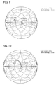
- FIG. 9 is a diagram illustrating one example of a result of the impedance matching process in the first example.
- FIG. 10 is a diagram illustrating one example of a result of impedance matching process in a comparative example.
- FIG. 11 is a diagram illustrating another example of the result of the impedance matching process in the first example.
- FIG. 12 is a diagram illustrating another example of the result of impedance matching process in the comparative example.
- Examples illustrated in FIG. 9 and FIG. 10 are those in a case where the initial value of the input impedance of the transmitting antenna 11 is 22 ⁇ (i.e. in a case where the impedance point Zin corresponding to the initial value of the input impedance is in the region B on the Smith chart (refer to FIG. 5 )).
- the theoretical value of the variable inductor L and the theoretical value of the variable capacitor C 2 are calculated.
- the matching of the impedance associated with the transmission circuit 10 requires 1.0 sec.
- the matching of the impedance associated with the transmission circuit 10 requires 3.2 sec.
- the impedance matching process in the example allows the impedance matching which requires about one third the time of the impedance matching process in the comparative example.
- Examples illustrated in FIG. 11 and FIG. 12 are those in a case where the initial value of the input impedance of the transmitting antenna 11 is 22 ⁇ (i.e. in a case where the impedance point Zin corresponding to the initial value of the input impedance is in the region A on the Smith chart (refer to FIG. 4 )).
- the theoretical value of the variable inductor L and the theoretical value of the variable capacitor C 1 are calculated.
- the impedance matching process in the example allows the impedance matching which requires about half the time of the impedance matching process in the comparative example.
- a second example of the impedance matching apparatus of the present invention will be explained on the basis of FIG. 13 .
- the second example is the same as the first example described above, except for having a partially different impedance matching process.
- a repetitive explanation will be omitted as occasion demands, and basically, a point different from the first example will be explained on the basis of FIG. 13 .
- the step 2 of the impedance matching process in the second example will be explained with reference to a flowchart in FIG. 13 .
- impedance matching using a steepest descent method is performed. Since the step 1 of the impedance matching process is the same as the step 1 of the impedance matching process in the first example described above, an explanation thereof will be omitted.
- the matching circuit set point calculator 140 sets respective initial values for variables L(m), C 1 ( m ) and C 2 ( m ) which correspond to the variable inductor L, the variable capacitor C 1 and the variable capacitor C 2 , respectively (step S 301 ).
- the respective initial values for the variables L(m), C 1 ( m ) and C 2 ( m ) are values obtained as a result of the step 1 of the impedance matching process.
- the matching circuit set point calculator 140 then sets respective values of the variable inductor L, the variable capacitor C 1 and the variable capacitor C 2 so as to correspond to the respective initial values for the variables L(m), C 1 ( m ) and C 2 ( m ), and then obtains a reflected power value Pr on the basis of the reflected signal extracted by the directional coupler 120 (step S 302 ).
- the matching circuit set point calculator 140 then sets respective values of the variable inductor L, the variable capacitor C 1 and the variable capacitor C 2 so as to correspond to the respective variables L(m+1), C 1 ( m +1) and C 2 ( m +1), and then obtains the reflected power value Pr on the basis of the reflected signal extracted by the directional coupler 120 (step S 316 ).
- the matching circuit set point calculator 140 determines whether or not the obtained reflected power value Pr is less than a threshold value Prthr (step S 317 ). If it is determined that the obtained reflected power value Pr is less than the threshold value Prthr (the step S 317 : Yes), the matching circuit set point calculator 140 ends the process. On the other hand, if it is determined that the obtained reflected power value Pr is greater than or equal to the threshold value Prthr (the step S 317 : No), the matching circuit set point calculator 140 performs the step S 303 described above.
- the present invention is not limited to wireless power transmission exemplified in the examples but can be applied to, for example, communication.
Landscapes
- Engineering & Computer Science (AREA)
- Computer Networks & Wireless Communication (AREA)
- Signal Processing (AREA)
- Power Engineering (AREA)
- Transmitters (AREA)
- Networks Using Active Elements (AREA)
Applications Claiming Priority (1)
| Application Number | Priority Date | Filing Date | Title |
|---|---|---|---|
| PCT/JP2012/072473 WO2014037994A1 (ja) | 2012-09-04 | 2012-09-04 | インピーダンス整合装置及び方法、並びにコンピュータプログラム |
Publications (2)
| Publication Number | Publication Date |
|---|---|
| US20150236728A1 US20150236728A1 (en) | 2015-08-20 |
| US9520905B2 true US9520905B2 (en) | 2016-12-13 |
Family
ID=50236647
Family Applications (1)
| Application Number | Title | Priority Date | Filing Date |
|---|---|---|---|
| US14/425,938 Active 2032-12-11 US9520905B2 (en) | 2012-09-04 | 2012-09-04 | Impedance matching apparatus and method, and computer program |
Country Status (3)
| Country | Link |
|---|---|
| US (1) | US9520905B2 (ja) |
| JP (1) | JP5856305B2 (ja) |
| WO (1) | WO2014037994A1 (ja) |
Cited By (2)
| Publication number | Priority date | Publication date | Assignee | Title |
|---|---|---|---|---|
| US20170331314A1 (en) * | 2016-05-12 | 2017-11-16 | Honeywell International Inc. | Auto-tunable wireless charger |
| US10736050B2 (en) | 2018-07-09 | 2020-08-04 | Honeywell International Inc. | Adjusting transmission power of an antenna based on an object causing path loss in a communication link |
Families Citing this family (13)
| Publication number | Priority date | Publication date | Assignee | Title |
|---|---|---|---|---|
| CN105850006A (zh) * | 2013-12-26 | 2016-08-10 | 三菱电机工程技术株式会社 | 高频电源用自动匹配电路 |
| US9401738B2 (en) * | 2014-07-15 | 2016-07-26 | Mediatek Singapore Pte. Ltd. | Method for simplified closed-loop antenna tuning |
| JP2016092803A (ja) * | 2014-11-11 | 2016-05-23 | 三菱重工業株式会社 | 整合回路及び無線通信装置 |
| JP6429419B2 (ja) * | 2015-02-27 | 2018-11-28 | 株式会社日立国際電気 | 整合器及び整合方法 |
| KR102048231B1 (ko) * | 2015-06-30 | 2019-11-25 | 가부시키가이샤 히다치 고쿠사이 덴키 | 정합기 및 정합 방법 |
| DE102015220847A1 (de) * | 2015-10-26 | 2017-04-27 | TRUMPF Hüttinger GmbH + Co. KG | Verfahren zur Impedanzanpassung einer Last an die Ausgangsimpedanz eines Leistungsgenerators und Impedanzanpassungsanordnung |
| US10840874B2 (en) * | 2016-03-18 | 2020-11-17 | Hitachi Kokusai Electric Inc. | Matching device |
| US10355662B2 (en) * | 2016-12-06 | 2019-07-16 | Honeywell International Inc. | Impedance matching using tunable elements |
| TWI641217B (zh) * | 2017-09-15 | 2018-11-11 | 瑞柯科技股份有限公司 | 具備同軸纜線供電功能的電子裝置 |
| CN109474731A (zh) * | 2018-12-22 | 2019-03-15 | Oppo(重庆)智能科技有限公司 | 射频调试方法及相关产品 |
| CN110311646A (zh) * | 2019-06-28 | 2019-10-08 | 高斯贝尔数码科技股份有限公司 | 一种微波功率源与反应腔的自适应匹配方法及系统 |
| US11438850B2 (en) * | 2020-09-09 | 2022-09-06 | Samsung Electronics Co., Ltd. | Data-driven methods for look up table-free closed-loop antenna impedance tuning |
| DE102021201937A1 (de) * | 2021-03-01 | 2022-09-01 | TRUMPF Hüttinger GmbH + Co. KG | Verfahren zur Impedanzanpassung, Impedanzanpassungsanordnung und Plasmasystem |
Citations (15)
| Publication number | Priority date | Publication date | Assignee | Title |
|---|---|---|---|---|
| US4951009A (en) * | 1989-08-11 | 1990-08-21 | Applied Materials, Inc. | Tuning method and control system for automatic matching network |
| US5629653A (en) * | 1995-07-07 | 1997-05-13 | Applied Materials, Inc. | RF match detector circuit with dual directional coupler |
| JPH09134800A (ja) | 1995-11-08 | 1997-05-20 | Jeol Ltd | 高周波装置 |
| JP2001274651A (ja) | 2000-03-27 | 2001-10-05 | Japan Radio Co Ltd | インピーダンス整合装置、インピーダンス整合用コンダクタンス検出回路、およびインピーダンス整合方法 |
| US20030184319A1 (en) | 2002-02-08 | 2003-10-02 | Daihen Corporation | Impedance matching device provided with reactance-impedance table |
| JP2003318636A (ja) | 2002-02-22 | 2003-11-07 | Matsushita Electric Ind Co Ltd | ヘリカルアンテナ装置及びそれを備えた無線通信装置 |
| JP2004085446A (ja) | 2002-08-28 | 2004-03-18 | Daihen Corp | インピーダンス整合器の出力端特性解析方法、およびインピーダンス整合器、ならびにインピーダンス整合器の出力端特性解析システム |
| WO2004040693A1 (ja) | 2002-11-01 | 2004-05-13 | Fujitsu Limited | 制御装置および制御方法 |
| JP2010041558A (ja) | 2008-08-07 | 2010-02-18 | Yokohama National Univ | インピーダンス整合装置、およびインピーダンス整合方法 |
| US20100315280A1 (en) * | 2009-06-12 | 2010-12-16 | Khosrow Bakhtar | Multi-Platform Radar with Forced Resonating Antennas for Embedded Detection and Volumetric Imaging |
| US20110086600A1 (en) * | 2009-10-09 | 2011-04-14 | Texas Instruments Incorporated | Method and apparatus for antenna tuning |
| JP4856288B1 (ja) | 2010-08-10 | 2012-01-18 | パイオニア株式会社 | インピーダンス整合装置、制御方法 |
| US20140107638A1 (en) * | 2006-10-10 | 2014-04-17 | Medical Device Innovations Limited | Apparatus for treating tissue with microwave radiation and antenna calibration system and method |
| US20150109176A1 (en) * | 2013-10-21 | 2015-04-23 | Hong Kong Applied Science And Technology Research Institute Co. Ltd. | Antenna circuit and a method of optimisation thereof |
| US20160182003A1 (en) * | 2013-09-05 | 2016-06-23 | Murata Manufacturing Co., Ltd. | Impedance conversion circuit, antenna apparatus, and wireless communication apparatus |
Family Cites Families (2)
| Publication number | Priority date | Publication date | Assignee | Title |
|---|---|---|---|---|
| JP2011166382A (ja) * | 2010-02-08 | 2011-08-25 | Panasonic Corp | 送信装置及びそれを備える高周波無線通信システム |
| WO2012020476A1 (ja) * | 2010-08-10 | 2012-02-16 | パイオニア株式会社 | インピーダンス整合装置、制御方法 |
-
2012
- 2012-09-04 US US14/425,938 patent/US9520905B2/en active Active
- 2012-09-04 JP JP2014534063A patent/JP5856305B2/ja active Active
- 2012-09-04 WO PCT/JP2012/072473 patent/WO2014037994A1/ja active Application Filing
Patent Citations (15)
| Publication number | Priority date | Publication date | Assignee | Title |
|---|---|---|---|---|
| US4951009A (en) * | 1989-08-11 | 1990-08-21 | Applied Materials, Inc. | Tuning method and control system for automatic matching network |
| US5629653A (en) * | 1995-07-07 | 1997-05-13 | Applied Materials, Inc. | RF match detector circuit with dual directional coupler |
| JPH09134800A (ja) | 1995-11-08 | 1997-05-20 | Jeol Ltd | 高周波装置 |
| JP2001274651A (ja) | 2000-03-27 | 2001-10-05 | Japan Radio Co Ltd | インピーダンス整合装置、インピーダンス整合用コンダクタンス検出回路、およびインピーダンス整合方法 |
| US20030184319A1 (en) | 2002-02-08 | 2003-10-02 | Daihen Corporation | Impedance matching device provided with reactance-impedance table |
| JP2003318636A (ja) | 2002-02-22 | 2003-11-07 | Matsushita Electric Ind Co Ltd | ヘリカルアンテナ装置及びそれを備えた無線通信装置 |
| JP2004085446A (ja) | 2002-08-28 | 2004-03-18 | Daihen Corp | インピーダンス整合器の出力端特性解析方法、およびインピーダンス整合器、ならびにインピーダンス整合器の出力端特性解析システム |
| WO2004040693A1 (ja) | 2002-11-01 | 2004-05-13 | Fujitsu Limited | 制御装置および制御方法 |
| US20140107638A1 (en) * | 2006-10-10 | 2014-04-17 | Medical Device Innovations Limited | Apparatus for treating tissue with microwave radiation and antenna calibration system and method |
| JP2010041558A (ja) | 2008-08-07 | 2010-02-18 | Yokohama National Univ | インピーダンス整合装置、およびインピーダンス整合方法 |
| US20100315280A1 (en) * | 2009-06-12 | 2010-12-16 | Khosrow Bakhtar | Multi-Platform Radar with Forced Resonating Antennas for Embedded Detection and Volumetric Imaging |
| US20110086600A1 (en) * | 2009-10-09 | 2011-04-14 | Texas Instruments Incorporated | Method and apparatus for antenna tuning |
| JP4856288B1 (ja) | 2010-08-10 | 2012-01-18 | パイオニア株式会社 | インピーダンス整合装置、制御方法 |
| US20160182003A1 (en) * | 2013-09-05 | 2016-06-23 | Murata Manufacturing Co., Ltd. | Impedance conversion circuit, antenna apparatus, and wireless communication apparatus |
| US20150109176A1 (en) * | 2013-10-21 | 2015-04-23 | Hong Kong Applied Science And Technology Research Institute Co. Ltd. | Antenna circuit and a method of optimisation thereof |
Non-Patent Citations (1)
| Title |
|---|
| International Search Report PCT/JP2012/072473 dated Dec. 11, 2012. |
Cited By (3)
| Publication number | Priority date | Publication date | Assignee | Title |
|---|---|---|---|---|
| US20170331314A1 (en) * | 2016-05-12 | 2017-11-16 | Honeywell International Inc. | Auto-tunable wireless charger |
| US10320229B2 (en) * | 2016-05-12 | 2019-06-11 | Honeywell International Inc. | Auto-tunable wireless charger |
| US10736050B2 (en) | 2018-07-09 | 2020-08-04 | Honeywell International Inc. | Adjusting transmission power of an antenna based on an object causing path loss in a communication link |
Also Published As
| Publication number | Publication date |
|---|---|
| WO2014037994A1 (ja) | 2014-03-13 |
| JP5856305B2 (ja) | 2016-02-09 |
| JPWO2014037994A1 (ja) | 2016-08-08 |
| US20150236728A1 (en) | 2015-08-20 |
Similar Documents
| Publication | Publication Date | Title |
|---|---|---|
| US9520905B2 (en) | Impedance matching apparatus and method, and computer program | |
| CN107231168B (zh) | 一种自干扰信号的消除装置及消除方法 | |
| US20150229289A1 (en) | Impedance matching device and control method | |
| US9484881B2 (en) | Impedance matching device and control method | |
| US20120256659A1 (en) | Current share compensation design | |
| RU2016113777A (ru) | Способы и устройства для определения устранения неисправности в линии электропередачи с поперечной компенсацией | |
| WO2015160616A1 (en) | Transformer parameter estimation using terminal measurements | |
| EP3561730B1 (fr) | Procédé de réglage de la phase du signal émis par un objet capable de communiquer sans contact avec un lecteur par modulation active de charge, et objet correspondant | |
| US10009000B2 (en) | RFID reader antenna port isolation | |
| US9935798B2 (en) | Automatic impedance matching for a radiofrequency reception chain | |
| CN105896086B (zh) | 阻抗的匹配方法及装置 | |
| WO2017060155A1 (en) | Improvements in or relating to direct current distance protection controllers | |
| EP3300190A1 (en) | Method of controlling gain of fiber amplifier and device utilizing same | |
| CN107210153A (zh) | 用于估计电路断路器的电操作时间的方法 | |
| CN106972870B (zh) | 一种天线调谐电路、移动终端及天线调谐方法 | |
| CN107342460B (zh) | 天线调谐控制方法、装置及系统 | |
| CA3034871C (en) | A method for phase controlled energizing of power transformer | |
| KR101299610B1 (ko) | 병행 2회선 송전선로의 자기단 등가전원 임피던스 추정 방법 | |
| CN103039012A (zh) | 实时补偿远程无线电单元中滤波器单元的频率响应的方法和装置 | |
| CN103493322B (zh) | 控制高压电网络中的电流中断设备的方法 | |
| CN107707251B (zh) | 一种信号发射功率控制方法及装置 | |
| CN104124765A (zh) | 无线电能传输系统的功率调节方法及系统 | |
| CN108256368B (zh) | 双端口网络的生成方法及装置 | |
| JP2017135117A (ja) | 高周波整合システムのインピーダンス調整方法 | |
| US10205347B2 (en) | Power supply device and power supply method |
Legal Events
| Date | Code | Title | Description |
|---|---|---|---|
| AS | Assignment |
Owner name: PIONEER CORPORATION, JAPAN Free format text: ASSIGNMENT OF ASSIGNORS INTEREST;ASSIGNOR:SUZUKI, MASAMI;REEL/FRAME:035212/0099 Effective date: 20150311 |
|
| STCF | Information on status: patent grant |
Free format text: PATENTED CASE |
|
| FEPP | Fee payment procedure |
Free format text: PAYOR NUMBER ASSIGNED (ORIGINAL EVENT CODE: ASPN); ENTITY STATUS OF PATENT OWNER: LARGE ENTITY |
|
| MAFP | Maintenance fee payment |
Free format text: PAYMENT OF MAINTENANCE FEE, 4TH YEAR, LARGE ENTITY (ORIGINAL EVENT CODE: M1551); ENTITY STATUS OF PATENT OWNER: LARGE ENTITY Year of fee payment: 4 |
|
| AS | Assignment |
Owner name: PIONEER CORPORATION, JAPAN Free format text: CHANGE OF ADDRESS;ASSIGNOR:PIONEER CORPORATION;REEL/FRAME:059614/0902 Effective date: 20160628 |
|
| AS | Assignment |
Owner name: TOYOTA JIDOSHA KABUSHIKI KAISHA, JAPAN Free format text: ASSIGNMENT OF ASSIGNORS INTEREST;ASSIGNOR:PIONEER CORPORATION;REEL/FRAME:059610/0634 Effective date: 20220415 |
|
| MAFP | Maintenance fee payment |
Free format text: PAYMENT OF MAINTENANCE FEE, 8TH YEAR, LARGE ENTITY (ORIGINAL EVENT CODE: M1552); ENTITY STATUS OF PATENT OWNER: LARGE ENTITY Year of fee payment: 8 |