US9474147B2 - Socket for semiconductor component, printed circuit board unit, and information processing apparatus - Google Patents
Socket for semiconductor component, printed circuit board unit, and information processing apparatus Download PDFInfo
- Publication number
- US9474147B2 US9474147B2 US14/684,470 US201514684470A US9474147B2 US 9474147 B2 US9474147 B2 US 9474147B2 US 201514684470 A US201514684470 A US 201514684470A US 9474147 B2 US9474147 B2 US 9474147B2
- Authority
- US
- United States
- Prior art keywords
- semiconductor component
- shield
- socket
- main surface
- insulator
- Prior art date
- Legal status (The legal status is an assumption and is not a legal conclusion. Google has not performed a legal analysis and makes no representation as to the accuracy of the status listed.)
- Active
Links
Images


Classifications
-
- H—ELECTRICITY
- H05—ELECTRIC TECHNIQUES NOT OTHERWISE PROVIDED FOR
- H05K—PRINTED CIRCUITS; CASINGS OR CONSTRUCTIONAL DETAILS OF ELECTRIC APPARATUS; MANUFACTURE OF ASSEMBLAGES OF ELECTRICAL COMPONENTS
- H05K1/00—Printed circuits
- H05K1/02—Details
- H05K1/0213—Electrical arrangements not otherwise provided for
- H05K1/0216—Reduction of cross-talk, noise or electromagnetic interference
-
- H—ELECTRICITY
- H01—ELECTRIC ELEMENTS
- H01R—ELECTRICALLY-CONDUCTIVE CONNECTIONS; STRUCTURAL ASSOCIATIONS OF A PLURALITY OF MUTUALLY-INSULATED ELECTRICAL CONNECTING ELEMENTS; COUPLING DEVICES; CURRENT COLLECTORS
- H01R12/00—Structural associations of a plurality of mutually-insulated electrical connecting elements, specially adapted for printed circuits, e.g. printed circuit boards [PCB], flat or ribbon cables, or like generally planar structures, e.g. terminal strips, terminal blocks; Coupling devices specially adapted for printed circuits, flat or ribbon cables, or like generally planar structures; Terminals specially adapted for contact with, or insertion into, printed circuits, flat or ribbon cables, or like generally planar structures
- H01R12/70—Coupling devices
- H01R12/7076—Coupling devices for connection between PCB and component, e.g. display
-
- H—ELECTRICITY
- H01—ELECTRIC ELEMENTS
- H01R—ELECTRICALLY-CONDUCTIVE CONNECTIONS; STRUCTURAL ASSOCIATIONS OF A PLURALITY OF MUTUALLY-INSULATED ELECTRICAL CONNECTING ELEMENTS; COUPLING DEVICES; CURRENT COLLECTORS
- H01R12/00—Structural associations of a plurality of mutually-insulated electrical connecting elements, specially adapted for printed circuits, e.g. printed circuit boards [PCB], flat or ribbon cables, or like generally planar structures, e.g. terminal strips, terminal blocks; Coupling devices specially adapted for printed circuits, flat or ribbon cables, or like generally planar structures; Terminals specially adapted for contact with, or insertion into, printed circuits, flat or ribbon cables, or like generally planar structures
- H01R12/70—Coupling devices
- H01R12/7082—Coupling device supported only by cooperation with PCB
-
- H—ELECTRICITY
- H01—ELECTRIC ELEMENTS
- H01R—ELECTRICALLY-CONDUCTIVE CONNECTIONS; STRUCTURAL ASSOCIATIONS OF A PLURALITY OF MUTUALLY-INSULATED ELECTRICAL CONNECTING ELEMENTS; COUPLING DEVICES; CURRENT COLLECTORS
- H01R13/00—Details of coupling devices of the kinds covered by groups H01R12/70 or H01R24/00 - H01R33/00
- H01R13/648—Protective earth or shield arrangements on coupling devices, e.g. anti-static shielding
- H01R13/658—High frequency shielding arrangements, e.g. against EMI [Electro-Magnetic Interference] or EMP [Electro-Magnetic Pulse]
- H01R13/6581—Shield structure
- H01R13/6585—Shielding material individually surrounding or interposed between mutually spaced contacts
- H01R13/6588—Shielding material individually surrounding or interposed between mutually spaced contacts with through openings for individual contacts
-
- H—ELECTRICITY
- H05—ELECTRIC TECHNIQUES NOT OTHERWISE PROVIDED FOR
- H05K—PRINTED CIRCUITS; CASINGS OR CONSTRUCTIONAL DETAILS OF ELECTRIC APPARATUS; MANUFACTURE OF ASSEMBLAGES OF ELECTRICAL COMPONENTS
- H05K7/00—Constructional details common to different types of electric apparatus
- H05K7/02—Arrangements of circuit components or wiring on supporting structure
- H05K7/10—Plug-in assemblages of components, e.g. IC sockets
- H05K7/1053—Plug-in assemblages of components, e.g. IC sockets having interior leads
- H05K7/1061—Plug-in assemblages of components, e.g. IC sockets having interior leads co-operating by abutting
- H05K7/1069—Plug-in assemblages of components, e.g. IC sockets having interior leads co-operating by abutting with spring contact pieces
-
- H—ELECTRICITY
- H01—ELECTRIC ELEMENTS
- H01R—ELECTRICALLY-CONDUCTIVE CONNECTIONS; STRUCTURAL ASSOCIATIONS OF A PLURALITY OF MUTUALLY-INSULATED ELECTRICAL CONNECTING ELEMENTS; COUPLING DEVICES; CURRENT COLLECTORS
- H01R12/00—Structural associations of a plurality of mutually-insulated electrical connecting elements, specially adapted for printed circuits, e.g. printed circuit boards [PCB], flat or ribbon cables, or like generally planar structures, e.g. terminal strips, terminal blocks; Coupling devices specially adapted for printed circuits, flat or ribbon cables, or like generally planar structures; Terminals specially adapted for contact with, or insertion into, printed circuits, flat or ribbon cables, or like generally planar structures
- H01R12/50—Fixed connections
- H01R12/51—Fixed connections for rigid printed circuits or like structures
- H01R12/52—Fixed connections for rigid printed circuits or like structures connecting to other rigid printed circuits or like structures
-
- H—ELECTRICITY
- H01—ELECTRIC ELEMENTS
- H01R—ELECTRICALLY-CONDUCTIVE CONNECTIONS; STRUCTURAL ASSOCIATIONS OF A PLURALITY OF MUTUALLY-INSULATED ELECTRICAL CONNECTING ELEMENTS; COUPLING DEVICES; CURRENT COLLECTORS
- H01R13/00—Details of coupling devices of the kinds covered by groups H01R12/70 or H01R24/00 - H01R33/00
- H01R13/02—Contact members
- H01R13/22—Contacts for co-operating by abutting
- H01R13/24—Contacts for co-operating by abutting resilient; resiliently-mounted
- H01R13/2435—Contacts for co-operating by abutting resilient; resiliently-mounted with opposite contact points, e.g. C beam
-
- H01R9/096—
Definitions
- the embodiments discussed herein are related to a socket for a semiconductor component, a printed circuit board unit, and an information processing apparatus.
- sockets include, for example, LGA (Land Grid Array) sockets and BGA (Ball Grid Array) sockets.
- a plurality of conductive terminals are provided so that a semiconductor component and a printed circuit board may be electrically connected.
- the terminals are provided to correspond to electrodes of the semiconductor component, and include signal terminals, grounding terminals and the like, for example.
- signal terminals are preferably protected from noise as much as possible.
- a socket for a semiconductor component including a plate-shaped insulator having a first main surface and a second main surface, where the first main surface and the second main surface being a top surface and a bottom surface of the insulator, and a through hole being formed in the insulator, a terminal inserted in the through hole, the terminal having one end configured to be connected to a signal electrode of the semiconductor component and having another end configured to be connected to a signal electrode of a printed circuit board, and a shield buried in the insulator to surround the terminal from sides of the terminal, the shield including a first contact protruding from the first main surface and configured to be connected to a ground electrode of the semiconductor component, and a second contact protruding from the second main surface and configured to be connected to a ground electrode of the printed circuit board.
- a printed circuit board unit including a printed circuit board, and a socket for a semiconductor component connected to the printed circuit board
- the socket for the semiconductor component includes a plate-shaped insulator having a first main surface and a second main surface, where the first main surface and the second main surface being a top surface and a bottom surface of the insulator, and a through hole being formed in the insulator, a terminal inserted in the through hole, the terminal having one end configured to be connected to a signal electrode of the semiconductor component and having another end connected to a signal electrode of the printed circuit board, and a shield buried in the insulator to surround the terminal from sides of the terminal, the shield including a first contact protruding from the first main surface and configured to be connected to a ground electrode of the semiconductor component and a second contact protruding from the second main surface and connected to a ground electrode of the printed circuit board.
- an information processing apparatus including a printed circuit board, a semiconductor component, and a socket for the semiconductor component connected to the printed circuit board, the semiconductor component being attached to the socket for the semiconductor component
- the socket for the semiconductor component includes a plate-shaped insulator having a first main surface and a second main surface, where the first main surface and the second main surface being a top surface and a bottom surface of the insulator, and a through hole being formed in the insulator, a terminal inserted in the through hole, the terminal having one end connected to a signal electrode of the semiconductor component and having another end connected to a signal electrode of the printed circuit board, and a shield buried in the insulator to surround the terminal from sides of the terminal, the shield including a first contact protruding from the first main surface and connected to a ground electrode of the semiconductor component and a second contact protruding from the second main surface and connected to a ground electrode of the printed circuit board.
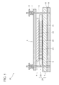
- FIG. 1 is a cross-sectional view of an information processing apparatus using a socket for semiconductor component with shielding
- FIG. 2 is a perspective view of a tip of terminals and their surroundings
- FIG. 3 is a plan view illustrating the arrangement of electrodes of a semiconductor component and terminals of the socket for semiconductor component
- FIG. 4 is a schematic perspective view of a socket for semiconductor component examined by the inventors of the present application.
- FIG. 5 is a cross-sectional view of an information processing apparatus according to a first embodiment
- FIG. 6 is a perspective view of a socket for semiconductor component according to the first embodiment
- FIG. 7 is an enlarged cross-sectional view of terminals provided in the socket for semiconductor component according to the first embodiment and surroundings thereof;
- FIG. 8 is a partially cross-sectional side view which illustrates an insulator and surroundings thereof and which is taken along a cross section different from that of FIG. 7 ;
- FIG. 9 is a perspective view of a first shield plate provided in the socket for semiconductor component according to the first embodiment.
- FIG. 10 is a perspective view of a second shield plate provided in the socket for semiconductor component according to the first embodiment
- FIG. 11 is a schematic perspective view illustrating the positional relationship among terminals, first shield plates, and second shield plates in the first embodiment
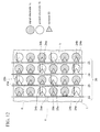
- FIG. 12 is a plan view illustrating the arrangement of electrodes of a printed circuit board, terminals, the first shield plates, and the second shield plates in the first embodiment;
- FIG. 13 is a plan view of the socket for semiconductor component in the course of manufacturing thereof according to the first embodiment
- FIGS. 14A to 14E are perspective views of the socket for semiconductor component in the course of manufacturing thereof according to the first embodiment
- FIG. 15 is a plan view illustrating the arrangement of electrodes of the printed circuit board, terminals, and first shield plates for the case where a shield is formed only by first shield plates in the first embodiment;
- FIG. 16 is a partially cross-sectional side view taken along line I-I of FIG. 15 ;
- FIG. 17 is a schematic perspective view of a socket for semiconductor component according to a second embodiment
- FIG. 18 is a perspective view of a first shield plate provided in the socket for semiconductor component according to the second embodiment
- FIG. 19 is a developed view of the first shield plate provided in the socket for semiconductor component according to the second embodiment.
- FIG. 20 is an enlarged cross-sectional view of an information processing apparatus including the socket for semiconductor component according to the second embodiment
- FIG. 21 is a partially cross-sectional side view which illustrates an insulator and surroundings thereof and which is taken along a cross section different from that of FIG. 20 ;
- FIG. 22 is a schematic perspective view of a socket for semiconductor component according to a third embodiment
- FIG. 23 is a perspective view of a first shield plate provided in the socket for semiconductor component according to the third embodiment.
- FIG. 24 is a partially cross-sectional side view taken along line II-II of FIG. 23 ;
- FIG. 25 is a developed view of the first shield plate provided in the socket for semiconductor component according to the third embodiment.
- FIG. 26 is a partially cross-sectional side view of an information processing apparatus according to the third embodiment.
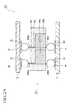
- FIG. 27 is a schematic perspective view of a socket for semiconductor component according to a fourth embodiment
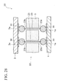
- FIG. 28 is an enlarged cross-sectional view of an information processing apparatus according to the fourth embodiment.
- FIG. 29 is a partially cross-sectional side view which illustrates an insulator and surroundings thereof and which is taken along a cross section different from that of FIG. 28 ;
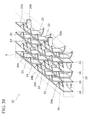
- FIG. 30 is a schematic perspective view of a socket for semiconductor component according to another embodiment.
- a socket for the semiconductor component such as an LGA socket
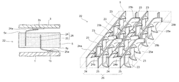
- FIG. 1 is a cross-sectional view of an information processing apparatus 10 using a socket for semiconductor component with the above-described shielding.
- This information processing apparatus 10 is a server or a personal computer, and includes a printed circuit board 1 and a semiconductor component 3 such as a CPU attached to the printed circuit board 1 with a socket 2 for a semiconductor component interposed therebetween.
- a semiconductor component 3 such as a CPU attached to the printed circuit board 1 with a socket 2 for a semiconductor component interposed therebetween.
- the printed circuit board 1 is a circuit board such as a mother board, and includes unillustrated interconnections electrically connected to the semiconductor component 3 through the socket 2 .
- the socket 2 for the semiconductor component is an LGA socket, and has a structure in which a plurality of signal terminals 8 a and a plurality of ground terminals 8 b are buried in a plate-shaped resin insulator 5 .
- terminals 8 a and 8 b are pieces of metal such as copper which have spring properties, and can elastically deform in the thickness direction of the socket 2 for the semiconductor component. Further, the contact of the terminals 8 a and 8 b with each of the printed circuit board 1 and the semiconductor component 3 by elastic forces thereof causes the printed circuit board 1 and the semiconductor component 3 to be electrically connected to each other.
- signal electrodes 3 a and ground electrodes 3 b are provided on the semiconductor component 3 . Then, signal electrodes 1 a and ground electrodes 1 b are provided on the printed circuit board 1 to face the electrodes 3 a and 3 b , respectively.
- the signal electrodes 1 a are electrodes for exclusively sending and receiving signals to and from the semiconductor component 3 , and are connected to the signal electrodes 3 a of the semiconductor component 3 through the aforementioned signal terminals 8 a , respectively.
- the ground electrodes 1 b are electrodes for grounding the semiconductor component 3 , and are connected to the ground electrodes 3 b of the semiconductor component 3 through the aforementioned ground terminals 8 b.
- terminals 8 a and 8 b are merely in contact with the printed circuit board 1 and the semiconductor component 3 by the elastic forces thereof, and are not fixed to either the printed circuit board 1 or the semiconductor component 3 .
- a plate 4 is provided on a back surface of the semiconductor component 3
- a back plate 13 is provided on a back surface of the printed circuit board 1 with an insulating sheet 12 interposed therebetween.
- screws 6 are inserted through the plate 4 , and one ends of the screws 6 are fixed to the back plate 13 .
- nuts are provided on another ends of the screws 6 .
- the semiconductor component 3 is pressed toward the printed circuit board 1 by biasing forces of springs 7 provided between the nuts 9 and the plate 4 .
- the socket 2 for the semiconductor component since neither the printed circuit board 1 nor the semiconductor component 3 is fixed to the terminals 8 a and 8 b , the socket 2 for the semiconductor component is attachable to and detachable from the printed circuit board 1 and the semiconductor component 3 .
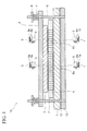
- FIG. 2 is a perspective view of a tip of terminals 8 a and 8 b and their surroundings.
- the terminal 8 a and 8 b protrudes from a surface of the insulator 5 , and the tip of the terminal 8 a and 8 b is bend to be directed in a direction along the surface of the insulator 5 .
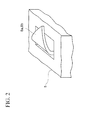
- FIG. 3 is a plan view illustrating the arrangement of the electrodes 3 a and 3 b of the semiconductor component 3 and the terminals 8 a and 8 b of the socket 2 for the semiconductor component.
- the electrodes 3 a and 3 b are formed in circular shapes by patterning a conductive film such as a copper film, and arranged in the form of a grid on a surface of the semiconductor component 3 . Further, the terminals 8 a and 8 b are also arranged in the form of a grid in planar view in accordance with the arrangement of the electrodes 3 a and 3 b.
- differential signals are supplied to two central signal electrodes 3 a .
- These signal electrodes 3 a are surrounded by ten ground electrodes 3 b .
- This provides a structure in which signal terminals 8 a are surrounded by ground terminals 8 b . Accordingly, the signal terminals 8 a are shielded with the ten ground terminals 8 b , and noise introduced to the signal terminals 8 a can be reduced.
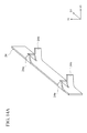
- the inventors of the present application examined the socket 2 for the semiconductor component illustrated in FIG. 4 .
- FIG. 4 is a schematic perspective view of the socket 2 for the semiconductor component examined by the inventors of the present application.
- the shield plates 11 a and 11 b extend in row and column directions of the arrangement of the terminals 8 a and 8 b , and are formed by machining a metal plate such as a copper plate.
- this structure eliminates the need to provide the ground electrodes 3 b for shielding on the semiconductor component 3 for the purpose of shielding the signal terminals 8 a . Accordingly, more signal electrodes 3 a can be provided on the semiconductor component 3 than in the case of FIG. 3 .
- the shield plates 11 a and 11 b are not electrically connected to other components. Accordingly, the electric potentials of the shield plates 11 a and 11 b fluctuate rather than becoming the ground potential, and noise may be introduced to the signal terminals 8 a inside the shield plates 11 a and 11 b.
- FIG. 5 is a cross-sectional view of an information processing apparatus 20 according to the present embodiment. It should be noted that in FIG. 5 , the same components as those described in FIG. 1 are denoted by the same reference numerals as those in FIG. 1 , and will not be further described below.
- the information processing apparatus 20 is a server or a personal computer, and includes a printed circuit board unit 21 .
- the printed circuit board unit 21 includes a printed circuit board 1 and a socket 22 for the semiconductor component provided thereon, and a semiconductor component 3 is attached to the socket 22 for the semiconductor component.
- the type of the semiconductor component 3 is not particularly limited, and a CPU, a GPU, or the like can be used as the semiconductor component 3 .
- the socket 22 for the semiconductor component is an LGA socket, and includes a plate-shaped resin insulator 5 and terminals 23 .
- the terminals 23 are pieces of metal such as copper which have spring properties, and are pressed to each of the printed circuit board 1 and the semiconductor component 3 by biasing forces of springs 7 .
- the socket 22 for the semiconductor component is not fixed to either the printed circuit board 1 or the semiconductor component 3 , and the socket 22 is attachable to and detachable from the printed circuit board 1 and the semiconductor component 3 .
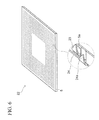
- FIG. 6 is a perspective view of the socket 22 for the semiconductor component.
- the insulator 5 of the socket 22 has through hole 5 a , and the aforementioned terminals 23 protrude from the through holes 5 a.
- the material of the insulator 5 is not particularly limited.
- the insulator 5 can be made of insulating resin material such as LCP (Liquid Crystal Polymer).
- first shield plates 24 made of copper or the like are buried in the insulator 5 .
- the first shield plates 24 function as part of a shield electromagnetically shielding the terminals 23 as described later.
- the first shield plates 24 have first contacts 24 a for grounding which protrude from the insulator 5 .
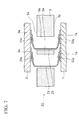
- FIG. 7 is an enlarged cross-sectional view of terminals 23 and their surroundings.
- the insulator 5 has a first main surface 5 x and a second main surface 5 y , which are a top surface and a bottom surface of the insulator 5 respectively.
- One end 23 x and another end 23 y of each of the aforementioned terminals 23 protrude from the main surfaces 5 x and 5 y , respectively.
- signal electrodes 1 a and 3 a are provided on the printed circuit board 1 and the semiconductor component 3 , respectively.
- the one end 23 x of the terminal 23 comes in contact with the corresponding signal electrode 3 a of the semiconductor component 3 , and the another end 23 y of the terminal 23 comes in contact with the corresponding signal electrode 1 a of the printed circuit board 1 .
- the signal electrodes 1 a and 3 a are electrically connected through the terminal 23 .
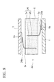
- FIG. 8 is a partially cross-sectional side view which illustrates the insulator 5 and its surroundings and which is taken along a cross section different from that of FIG. 7 .
- second shield plates 25 are buried in the insulator 5 . These shield plates 24 and 25 constitute a shield 26 .
- the first shield plates 24 are buried from the one main surface 5 x of the insulator 5 such that the first contacts 24 a protrude from the main surface 5 x . Further, the first contacts 24 a are brought into contact with ground electrodes 3 b of the semiconductor component 3 so that the first shield plates 24 is at the ground potential.
- the second shield plates 25 are buried in the insulator 5 from the other main surface 5 y.
- the second shield plates 25 have second contacts 25 a , and the second contacts 25 a are protruded from another main surface 5 y . Further, the second contacts 25 a are brought into contact with ground electrodes 1 b of the printed circuit board 1 so that the second shield plates 25 is at the ground potential.
- FIG. 9 is a perspective view of the first shield plate 24 .
- the first shield plate 24 is formed by machining a long copper plate extending in its longitudinal direction D 1 .
- First bent portions 24 b are provided in portions of the first shield plate 24 .
- both the first bent portions 24 b and the first contacts 24 a are directed in a normal direction D 3 of the first shield plate 24 by bending portions of the aforementioned copper plate. Bending the first contacts 24 a in this way can give spring properties to the first contacts 24 a , and this spring properties enable the first contacts 24 a to be pressed against the ground electrodes 3 b (see FIG. 8 ).
- FIG. 10 is a perspective view of the second shield plate 25 .
- the second shield plate 25 is formed by machining a long copper plate extending in its longitudinal direction D 1 . Second bent portions 25 b are provided in portions of the second shield plate 25 .
- Both the second bent portions 25 b and the second contacts 25 a are directed in the normal direction D 3 of the second shield plate 25 by bending portions of the copper plate. This gives spring properties to the second contacts 25 a as in the first contacts 24 a , and this spring properties enable the second contacts 25 a to be pressed against the ground electrodes 1 b (see FIG. 8 ).
- FIG. 11 is a schematic perspective view illustrating the positional relationship among the terminals 23 , the first shield plates 24 , and the second shield plates 25 .
- the first shield plates 24 and the second shield plates 25 are parallel to each other, and the terminals 23 are disposed therebetween. Further, the first bent portions 24 b of the first shield plate 24 are directed toward an adjacent second shield plate 25 , and the second bent portions 25 b of the second shield plate 25 are directed toward an adjacent first shield plate 24 .
- FIG. 12 is a plan view illustrating the arrangement of the electrodes 1 a and 1 b of the printed circuit board 1 , the terminals 23 , the first shield plates 24 , and the second shield plates 25 .
- two signal electrodes 1 a are provided in each partial region R of the printed circuit board 1 , and these two signal electrodes 1 are used as the electrodes for differential signals.
- the terminal 23 on the signal electrodes 1 a is surrounded by the adjacent shield plates 24 and 25 and the bent portions 24 b and 25 b from the sides of the terminal 23 . Accordingly, the terminal 23 can be electromagnetically shielded with the shield 26 .
- the shield plates 24 and 25 are provided with the contacts 24 a and 25 a for grounding as described previously, these contacts 24 a and 25 a can be connected to the ground electrodes 1 b and 3 b of the printed circuit board 1 and the semiconductor component 3 .
- the shield plates 24 and 25 are maintained at the ground potential. Accordingly, the fluctuation of the electric potentials of the shield plates 24 and 25 can be reduced, and the terminal 23 in the partial region R can be reliably shielded with the shield plates 24 and 25 .
- the semiconductor component 3 such as a CPU or the like, since differential signals having a high resistant to noise are frequently employed, the practical benefit of shielding the signal electrodes 1 a for differential signals with the shield plates 24 and 25 is particularly high.
- the signal electrodes 3 a do not need to be surrounded by a plurality of ground electrodes 3 b in order to shield the terminals 23 as in the example of FIG. 3 , a large number of signal electrodes 1 a and 3 a can be disposed on the printed circuit board 1 and the semiconductor component 3 .
- shielding two signal electrodes 3 a for differential signals requires a space corresponding to twelve electrodes in total, including ten ground electrodes 3 b around the two signal electrodes 3 a .
- the shield 26 can be grounded through two ground electrodes 1 b at two opposite ends of the partial region R as illustrated in FIG. 12 , and shielding two signal electrodes 3 a for differential signals requires a space corresponding to only four electrodes.
- FIG. 13 is a plan view of the socket 22 for the semiconductor component in the course of manufacturing thereof.
- FIGS. 14A to 14E are perspective views of the socket 22 for the semiconductor component in the course of manufacturing thereof.
- a copper plate is machined to fabricate the first shield plate 24 including first protrusions 24 a and the first bent portions 24 b.
- a length L of the first shield plate 24 measured in the longitudinal direction D 1 of the first shield plate 24 is approximately 30 mm, a height H thereof is approximately 1 mm, and a height h of the protrusion 24 a is approximately 0.5 mm. Moreover, a thickness of the first shield plate 24 is approximately 20 ⁇ m.
- the first protrusions 24 a and the first bent portions 24 b are bent by machining.
- both the first protrusions 24 a and the first bent portions 24 b are directed in the normal direction D 3 of the first shield plate 24 .
- the protrusions 24 a and the bent portions 24 b may be bent at the same time as the fabrication of the first shield plate 24 in the step of FIG. 13 .
- the second shield plate 25 is fabricated by a machining method similar to that used for the aforementioned first shield plate 24 . It should be noted that dimensions of the second shield plate 25 are the same as the aforementioned ones of the first shield plate 24 , and will not be described here.
- the insulator 5 is prepared. Then, through holes 5 a , grooves 5 b , and recessed portions 5 c are formed in the insulator 5 .
- the through holes 5 a are formed to pass through the insulator 5 from one main surface 5 x thereof to another main surface 5 y thereof.
- each of the grooves 5 b is formed from one of the main surfaces 5 x and 5 y to an intermediate depth of the insulator 5 .
- the recessed portions 5 c are formed to communicate with the grooves 5 b.
- the through holes 5 a , the grooves 5 b , and the recessed portions 5 c may be formed in the insulator 5 by machining, or may by formed by injection molding or the like at the same time as the molding of the insulator 5 .
- the terminals 23 are inserted into the through holes 5 a of the insulator 5 .
- the first shield plates 24 are pressed into the grooves 5 b from the one main surface 5 x of the insulator 5 , and the second shield plates 25 are pressed into the grooves 5 b from another main surface 5 y.
- first bent portions 24 b of the shield plates 24 are fitted into the recessed portions 5 c of the insulator 5 .
- the shield plates 24 and 25 are pressed into the grooves 5 b of the insulator 5 in the step of FIG. 14E to bury these shield plates 24 and 25 in the insulator 5 .
- Burying the shield plates 24 and 25 by pressing can reduce the cost of the socket 22 for the semiconductor component compared to burying by insert molding, which requires mold cost.
- the shield 26 is formed of the first shield plate 24 and the second shield plate 25 in the example of FIG. 12 , the shield 26 may be formed only by the first shield plates 24 as described below.
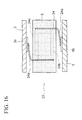
- FIG. 15 is a plan view illustrating the arrangement of the electrodes 1 a and 1 b of the printed circuit board 1 , the terminals 23 , and the first shield plates 24 for the case where the shield 26 is formed only by the first shield plates 24 as described above.
- one of the two adjacent first shield plates 24 is inverted to the other one, and the first bent portions 24 b of these first shield plates 24 are overlapped.
- This provides a structure in which the signal electrodes 1 a are surrounded by two adjacent first shield plates 24 and their first bent portions 24 b , and the signal electrodes 1 a can be electromagnetically shielded with the shield 26 .
- FIG. 16 is a partially cross-sectional side view taken along line I-I of FIG. 15 .
- the two adjacent first shield plates 24 are vertically inverted to each other, and the first contacts 24 a of the first shield plates 24 come in contact with the ground electrodes 3 b of the semiconductor component 3 .
- the socket 22 for the semiconductor component is attachable to and detachable from the printed circuit board 1 as described with reference to FIG. 5 .
- the socket 22 for the semiconductor component is fixed to the printed circuit board 1 as described below.
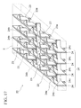
- FIG. 17 is a schematic perspective view of the socket for the semiconductor component according to the present embodiment.
- FIG. 17 the same components as those described in the first embodiment are denoted by the same reference numerals as those in the first embodiment, and will not be further described below. This is also the case for FIGS. 18 to 21 described below.
- the shield 26 is formed of a plurality of first shield plates 24 , and the terminals 23 are surrounded by the first shield plates 24 and their first bent portions 24 b . Accordingly, the terminals 23 can be electromagnetically shielded with the shield 26 as in the first embodiment.
- the second contacts 24 c are provided in the lower portions of the first shield plates 24 .
- the second contacts 24 c have the shape of a rectangular strip, and protrude from the bottom surface of the insulator 5 .
- first protrusions 23 a each having the shape of a rectangular strip are provided at lower ends of the terminals 23 .
- the first protrusions 23 a protrude from the bottom surface of the insulator 5 .
- FIG. 18 is a perspective view of the first shield plate 24 according to the present embodiment
- FIG. 19 is a developed view of the first shield plate 24 .
- the first shield plate 24 can be fabricated by machining a long copper plate extending in its longitudinal direction D 1 . Further, the first contacts 24 a , the first bent portions 24 b , and the second contacts 24 c are provided integrally with the copper plate.
- FIG. 20 is an enlarged cross-sectional view of an information processing apparatus 20 including this socket 22 for the semiconductor component.
- solder bumps 30 are fixed to the first protrusions 23 a of the terminals 23 . Further, the terminals 23 are fixed to the signal electrodes 1 a of the printed circuit board 1 with the solder bumps 30 .
- the signal electrodes 3 a of the semiconductor component 3 are merely in contact with the one ends 23 x of the terminals 23 , and the semiconductor component 3 is attachable to and detachable from the socket 22 .
- FIG. 21 is a partially cross-sectional side view which illustrates the insulator 5 and its surroundings, which is taken along a cross section different from that of FIG. 20 .
- solder bumps 30 are also fixed to the second contacts 24 c of the first shield plate 24 . Further, the first shield plates 24 are fixed to the ground electrodes 1 b of the printed circuit board 1 with the solder bumps 30 .
- the socket 22 fixed to the printed circuit board 1 with the solder bumps 30 as illustrated in FIGS. 20 and 21 is also called a BGA-type socket.
- the first shield plates 24 are fixed to the ground electrodes 1 b with the solder bumps 30 , the first shield plates 24 can be reliably grounded through the ground electrodes 1 b , and the fluctuation of the electric potentials of the first shield plates 24 can be reliably reduced.
- the first shield plates 24 are more reliably maintained at the ground potential as described below.
- FIG. 22 is a schematic perspective view of a socket for the semiconductor component according to the present embodiment.
- FIG. 22 the same components as those described in the first and second embodiments are denoted by the same reference numerals as those in these embodiments, and will not be further described below. This is also the case for FIGS. 22 to 25 described below.
- the shield 26 is formed of a plurality of first shield plates 24 , and the terminals 23 are electromagnetically shielded with the shield 26 , as in the second embodiment.
- FIG. 23 is a perspective view of the first shield plate 24 according to the present embodiment.
- the second contacts 24 c are provided in a lower portion of the first shield plate 24 . Further, both the first contacts 24 a and the first bent portions 24 b are directed in the normal direction D 3 of the first shield plate 24 .
- FIG. 24 is a partially cross-sectional side view taken along line II-II of FIG. 23 .
- third bent portions 24 d are provided in a lower portion of the first shield plate 24 .
- the third bent portions 24 d are provided by bending portions of the first shield plate 24 and directed in a direction opposite to that of the first contacts 24 a.
- FIG. 25 is a developed view of the first shield plate 24 .
- the first shield plate 24 is formed from a copper plate extending in its longitudinal direction D 1 . Further, the first contacts 24 a , the first bent portions 24 b , the second contacts 24 c , and the third bent portions 24 d are provided integrally with the copper plate.
- FIG. 26 is a partially cross-sectional side view of an information processing apparatus 20 including the socket 22 for the semiconductor component according to the present embodiment.
- the second contacts 24 c of the first shield plates 24 protrude from the bottom surface of the insulator 5 . Further, solder bumps 30 are fixed to the second contacts 24 c , and the ground electrodes 1 b and the first shield plates 24 are electrically connected through the solder bumps 30 .
- the aforementioned third bent portions 24 d are brought into contact with an adjacent first shield plate 24 so that the adjacent first shield plates 24 are electrically connected.
- the adjacent first shield plates 24 are electrically connected through the third bent portions 24 d as illustrated in FIG. 26 , differences between the electric potentials of the shield plates 24 are reduced, and adjacent shield plates 24 can be reliably grounded.
- the semiconductor component 3 is attachable to and detachable from the socket 22 , because the signal electrodes 3 a of the semiconductor component 3 are merely in contact with the terminals 23 as illustrated in, for example, FIG. 20 .
- the semiconductor component 33 is fixed to the socket 22 for the semiconductor component as described below.
- FIG. 27 is a schematic perspective view of the socket for the semiconductor component according to the present embodiment.
- FIG. 27 the same components as those described in the first to third embodiments are denoted by the same reference numerals as those in these embodiments, and will not be further described below. This is also the case for FIGS. 27 and 28 described below.
- the shield 26 is formed of a plurality of the first shield plates 24 , and the terminals 23 are electromagnetically shielded with the shield 26 , as in the second and third embodiments.
- each of the first contacts 24 a of the first shield plates 24 has the shape of a rectangular strip, and the first contacts 24 a are protruded from the top surface of the plate-shaped insulator 5 .
- second protrusions 23 b each having the shape of a rectangular strip are provided in the terminals 23 , and the second protrusions 23 b are protruded from the top surface of the insulator 5 .
- FIG. 28 is an enlarged cross-sectional view of an information processing apparatus 20 including this socket 22 for the semiconductor component.
- the first protrusions 23 a of the terminals 23 are fixed to the signal electrodes 1 a of the printed circuit board 1 with solder bumps 30 .
- solder bumps 30 are also fixed to the second protrusions 23 b of the terminals 23 , and the terminals 23 are fixed to the signal electrodes 3 a of the semiconductor component 3 with the solder bumps 30 .
- FIG. 29 is a partially cross-sectional side view which illustrates the insulator 5 and its surroundings, which is taken along a cross section different from that of FIG. 28 .
- a solder bump 30 is fixed to each of the first contacts 24 a and the second contacts 24 c of the first shield plates 24 . Further, the first shield plates 24 are fixed to the ground electrodes 1 b and 3 b of the printed circuit board 1 and the semiconductor component 3 with the solder bumps 30 .
- the first shield plates 24 are fixed to the ground electrodes 3 b of the semiconductor component 3 as illustrated in FIG. 29 . Accordingly, compared to the second and third embodiments, in which the first shield plates 24 are fixed only to the printed circuit board 1 , the first shield plates 24 can be reliably maintained at the ground potential, and the fluctuation of the electric potentials of the first shield plates 24 can be reduced.
- the first shield plates 24 and the second shield plates 25 are respectively protruded from the first main surface 5 x and the second main surface 5 y of the insulator 5 as illustrated in FIG. 8 .
- such a structure may be employed in which the shield plate is protruded from only one main surface of the insulator 5 .
- FIG. 30 is a schematic perspective view of the socket 22 for the semiconductor component for the case where the shield 26 is formed only by the first shield plates 24 with the first contacts 24 a of the first shield plates 24 being protruded only from the first main surface 5 x of the insulator 5 .
- the terminals 23 are surrounded by the first shield plates 24 and their first bent portions 24 b so that the terminals 23 can be shielded.
- the first contacts 24 a of the first shield plates 24 are brought into contact with the ground electrodes 3 b of the semiconductor component 3 (see FIG. 8 ), so that the first shield plates 24 are at the ground potential.
Landscapes
- Engineering & Computer Science (AREA)
- Microelectronics & Electronic Packaging (AREA)
- Physics & Mathematics (AREA)
- Electromagnetism (AREA)
- Connecting Device With Holders (AREA)
- Coupling Device And Connection With Printed Circuit (AREA)
- Details Of Connecting Devices For Male And Female Coupling (AREA)
Applications Claiming Priority (2)
| Application Number | Priority Date | Filing Date | Title |
|---|---|---|---|
| JP2014119608A JP6344072B2 (ja) | 2014-06-10 | 2014-06-10 | 半導体部品用ソケット、プリント基板ユニット、及び情報処理装置 |
| JP2014-119608 | 2014-06-10 |
Publications (2)
| Publication Number | Publication Date |
|---|---|
| US20150359122A1 US20150359122A1 (en) | 2015-12-10 |
| US9474147B2 true US9474147B2 (en) | 2016-10-18 |
Family
ID=54770720
Family Applications (1)
| Application Number | Title | Priority Date | Filing Date |
|---|---|---|---|
| US14/684,470 Active US9474147B2 (en) | 2014-06-10 | 2015-04-13 | Socket for semiconductor component, printed circuit board unit, and information processing apparatus |
Country Status (2)
| Country | Link |
|---|---|
| US (1) | US9474147B2 (ja) |
| JP (1) | JP6344072B2 (ja) |
Cited By (3)
| Publication number | Priority date | Publication date | Assignee | Title |
|---|---|---|---|---|
| US9837737B1 (en) * | 2016-10-28 | 2017-12-05 | Lotes Co., Ltd | Electrical connector |
| US10454218B2 (en) * | 2017-08-14 | 2019-10-22 | Foxconn Interconnect Technology Limited | Electrical connector and method making the same |
| US11291133B2 (en) * | 2018-03-28 | 2022-03-29 | Intel Corporation | Selective ground flood around reduced land pad on package base layer to enable high speed land grid array (LGA) socket |
Families Citing this family (3)
| Publication number | Priority date | Publication date | Assignee | Title |
|---|---|---|---|---|
| CN206461179U (zh) * | 2016-10-28 | 2017-09-01 | 番禺得意精密电子工业有限公司 | 电连接器 |
| CN110011095B (zh) * | 2019-04-09 | 2024-04-19 | 四川华丰科技股份有限公司 | 屏蔽板、模块结构及电连接器 |
| CN111817098B (zh) * | 2020-08-31 | 2020-11-27 | 上海燧原科技有限公司 | 一种电子负载 |
Citations (18)
| Publication number | Priority date | Publication date | Assignee | Title |
|---|---|---|---|---|
| JP2001326298A (ja) | 2000-05-18 | 2001-11-22 | Fujitsu Ltd | キャパシタ内蔵インターポーザ及びその製造方法 |
| US20040147140A1 (en) * | 2003-01-24 | 2004-07-29 | Zhineng Fan | Low inductance electrical contacts and lga connector system |
| US20040253845A1 (en) * | 2003-06-11 | 2004-12-16 | Brown Dirk D. | Remountable connector for land grid array packages |
| JP2006024654A (ja) | 2004-07-06 | 2006-01-26 | Tokyo Electron Ltd | インターポーザ |
| US20060046527A1 (en) * | 2004-08-25 | 2006-03-02 | Stone Brent S | Land grid array with socket plate |
| US20060154497A1 (en) * | 2005-01-11 | 2006-07-13 | Takashi Amemiya | Inspection contact structure and probe card |
| US20070246253A1 (en) | 2004-07-06 | 2007-10-25 | Masami Yakabe | Through Substrate, Interposer and Manufacturing Method of Through Substrate |
| US20090124100A1 (en) * | 2007-11-09 | 2009-05-14 | Mason Jeffery W | Shielded electrical interconnect |
| US20110070750A1 (en) * | 2009-09-23 | 2011-03-24 | Tyco Electronics Corporation | Electrical connector having a sequential mating interface |
| US20120184151A1 (en) * | 2011-01-18 | 2012-07-19 | Hon Hai Precision Industry Co., Ltd. | Electrical connector |
| US20130183861A1 (en) * | 2012-01-13 | 2013-07-18 | Yen-Chih Chang | Electrical connector with improved shielding means |
| US8491337B2 (en) * | 2011-03-14 | 2013-07-23 | Lotes Co., Ltd. | Electrical connector with shielded recessed portions |
| US8535093B1 (en) * | 2012-03-07 | 2013-09-17 | Tyco Electronics Corporation | Socket having sleeve assemblies |
| US20140017942A1 (en) * | 2012-07-11 | 2014-01-16 | Tyco Electronics Corporation | Socket connectors and methods of assembling socket connectors |
| US20140154918A1 (en) * | 2012-11-30 | 2014-06-05 | Hon Hai Precision Industry Co., Ltd. | Electrical connector having a plurality of absorbing material blocks |
| US20140162472A1 (en) * | 2012-12-12 | 2014-06-12 | Amphenol InterCon Systems, Inc. | Impedance Controlled LGA Interposer Assembly |
| US20140242816A1 (en) * | 2010-06-03 | 2014-08-28 | Hsio Technologies, Llc | Selective metalization of electrical connector or socket housing |
| US8821188B2 (en) * | 2012-03-07 | 2014-09-02 | Hon Hai Precision Industry Co., Ltd. | Electrical connector assembly used for shielding |
Family Cites Families (3)
| Publication number | Priority date | Publication date | Assignee | Title |
|---|---|---|---|---|
| JPS59128184U (ja) * | 1984-01-19 | 1984-08-29 | 山一電機工業株式会社 | コネクタ類に於るシ−ルド用導電格子の構造 |
| JPH0714586U (ja) * | 1993-08-11 | 1995-03-10 | 第一電子工業株式会社 | 高密度実装用コネクタ |
| US8727808B2 (en) * | 2011-07-13 | 2014-05-20 | Tyco Electronics Corporation | Electrical connector assembly for interconnecting an electronic module and an electrical component |
-
2014
- 2014-06-10 JP JP2014119608A patent/JP6344072B2/ja not_active Expired - Fee Related
-
2015
- 2015-04-13 US US14/684,470 patent/US9474147B2/en active Active
Patent Citations (18)
| Publication number | Priority date | Publication date | Assignee | Title |
|---|---|---|---|---|
| JP2001326298A (ja) | 2000-05-18 | 2001-11-22 | Fujitsu Ltd | キャパシタ内蔵インターポーザ及びその製造方法 |
| US20040147140A1 (en) * | 2003-01-24 | 2004-07-29 | Zhineng Fan | Low inductance electrical contacts and lga connector system |
| US20040253845A1 (en) * | 2003-06-11 | 2004-12-16 | Brown Dirk D. | Remountable connector for land grid array packages |
| JP2006024654A (ja) | 2004-07-06 | 2006-01-26 | Tokyo Electron Ltd | インターポーザ |
| US20070246253A1 (en) | 2004-07-06 | 2007-10-25 | Masami Yakabe | Through Substrate, Interposer and Manufacturing Method of Through Substrate |
| US20060046527A1 (en) * | 2004-08-25 | 2006-03-02 | Stone Brent S | Land grid array with socket plate |
| US20060154497A1 (en) * | 2005-01-11 | 2006-07-13 | Takashi Amemiya | Inspection contact structure and probe card |
| US20090124100A1 (en) * | 2007-11-09 | 2009-05-14 | Mason Jeffery W | Shielded electrical interconnect |
| US20110070750A1 (en) * | 2009-09-23 | 2011-03-24 | Tyco Electronics Corporation | Electrical connector having a sequential mating interface |
| US20140242816A1 (en) * | 2010-06-03 | 2014-08-28 | Hsio Technologies, Llc | Selective metalization of electrical connector or socket housing |
| US20120184151A1 (en) * | 2011-01-18 | 2012-07-19 | Hon Hai Precision Industry Co., Ltd. | Electrical connector |
| US8491337B2 (en) * | 2011-03-14 | 2013-07-23 | Lotes Co., Ltd. | Electrical connector with shielded recessed portions |
| US20130183861A1 (en) * | 2012-01-13 | 2013-07-18 | Yen-Chih Chang | Electrical connector with improved shielding means |
| US8535093B1 (en) * | 2012-03-07 | 2013-09-17 | Tyco Electronics Corporation | Socket having sleeve assemblies |
| US8821188B2 (en) * | 2012-03-07 | 2014-09-02 | Hon Hai Precision Industry Co., Ltd. | Electrical connector assembly used for shielding |
| US20140017942A1 (en) * | 2012-07-11 | 2014-01-16 | Tyco Electronics Corporation | Socket connectors and methods of assembling socket connectors |
| US20140154918A1 (en) * | 2012-11-30 | 2014-06-05 | Hon Hai Precision Industry Co., Ltd. | Electrical connector having a plurality of absorbing material blocks |
| US20140162472A1 (en) * | 2012-12-12 | 2014-06-12 | Amphenol InterCon Systems, Inc. | Impedance Controlled LGA Interposer Assembly |
Cited By (4)
| Publication number | Priority date | Publication date | Assignee | Title |
|---|---|---|---|---|
| US9837737B1 (en) * | 2016-10-28 | 2017-12-05 | Lotes Co., Ltd | Electrical connector |
| US10454218B2 (en) * | 2017-08-14 | 2019-10-22 | Foxconn Interconnect Technology Limited | Electrical connector and method making the same |
| US11291133B2 (en) * | 2018-03-28 | 2022-03-29 | Intel Corporation | Selective ground flood around reduced land pad on package base layer to enable high speed land grid array (LGA) socket |
| US11737227B2 (en) | 2018-03-28 | 2023-08-22 | Intel Corporation | Selective ground flood around reduced land pad on package base layer to enable high speed land grid array (LGA) socket |
Also Published As
| Publication number | Publication date |
|---|---|
| US20150359122A1 (en) | 2015-12-10 |
| JP6344072B2 (ja) | 2018-06-20 |
| JP2015232968A (ja) | 2015-12-24 |
Similar Documents
| Publication | Publication Date | Title |
|---|---|---|
| US9474147B2 (en) | Socket for semiconductor component, printed circuit board unit, and information processing apparatus | |
| US10886667B2 (en) | Board-connecting electric connector device | |
| US9178322B2 (en) | Electrical connector having improved shielding members | |
| US9614308B2 (en) | Board-connecting electric connector | |
| CN106921060B (zh) | 刚性-柔性电路连接器 | |
| TWI558026B (zh) | 相鄰訊號接點間具有接地屏蔽件之插座連接器 | |
| KR20200005646A (ko) | 전기 커넥터 장치 | |
| US9666964B2 (en) | Electrical receptacle connector | |
| US8814603B2 (en) | Shielding socket with two pieces contacts and two pieces housing components | |
| US9033737B2 (en) | Electrical connector | |
| US20120220169A1 (en) | Electronic component socket | |
| JP2014102916A (ja) | コネクタ及びフレキシブルプリント基板 | |
| TW201939829A (zh) | 電連接器 | |
| US9214747B2 (en) | Low profile electrical connector have a FPC | |
| US6971885B2 (en) | Interconnect device with opposingly oriented contacts | |
| US20150162679A1 (en) | Thin connector | |
| US7445463B2 (en) | Land grid array electrical connector | |
| TWI396339B (zh) | 連接器 | |
| US9431736B2 (en) | Card edge connector and card edge connector assembly | |
| KR102225366B1 (ko) | 리셉터클 커넥터 | |
| CN109687204B (zh) | 电连接器 | |
| US9118128B2 (en) | Electric connector having a reinforcement frame | |
| CN103311745A (zh) | 电连接器及其组件 | |
| TWI424617B (zh) | 電連接器 | |
| KR102317944B1 (ko) | 리셉터클 커넥터 및 이를 포함하는 전자 장치 |
Legal Events
| Date | Code | Title | Description |
|---|---|---|---|
| AS | Assignment |
Owner name: FUJITSU LIMITED, JAPAN Free format text: ASSIGNMENT OF ASSIGNORS INTEREST;ASSIGNORS:MASUDA, YASUSHI;TAMURA, AKIRA;MORITA, YOSHIHIRO;AND OTHERS;SIGNING DATES FROM 20150320 TO 20150324;REEL/FRAME:035562/0479 |
|
| STCF | Information on status: patent grant |
Free format text: PATENTED CASE |
|
| MAFP | Maintenance fee payment |
Free format text: PAYMENT OF MAINTENANCE FEE, 4TH YEAR, LARGE ENTITY (ORIGINAL EVENT CODE: M1551); ENTITY STATUS OF PATENT OWNER: LARGE ENTITY Year of fee payment: 4 |