US9444451B2 - Switch circuit - Google Patents
Switch circuit Download PDFInfo
- Publication number
- US9444451B2 US9444451B2 US14/469,207 US201414469207A US9444451B2 US 9444451 B2 US9444451 B2 US 9444451B2 US 201414469207 A US201414469207 A US 201414469207A US 9444451 B2 US9444451 B2 US 9444451B2
- Authority
- US
- United States
- Prior art keywords
- voltage
- node
- input
- input terminal
- terminal
- Prior art date
- Legal status (The legal status is an assumption and is not a legal conclusion. Google has not performed a legal analysis and makes no representation as to the accuracy of the status listed.)
- Active, expires
Links
Images


Classifications
-
- H—ELECTRICITY
- H03—ELECTRONIC CIRCUITRY
- H03K—PULSE TECHNIQUE
- H03K17/00—Electronic switching or gating, i.e. not by contact-making and –breaking
- H03K17/51—Electronic switching or gating, i.e. not by contact-making and –breaking characterised by the components used
- H03K17/56—Electronic switching or gating, i.e. not by contact-making and –breaking characterised by the components used by the use, as active elements, of semiconductor devices
- H03K17/687—Electronic switching or gating, i.e. not by contact-making and –breaking characterised by the components used by the use, as active elements, of semiconductor devices the devices being field-effect transistors
-
- H—ELECTRICITY
- H03—ELECTRONIC CIRCUITRY
- H03K—PULSE TECHNIQUE
- H03K17/00—Electronic switching or gating, i.e. not by contact-making and –breaking
- H03K17/06—Modifications for ensuring a fully conducting state
- H03K17/063—Modifications for ensuring a fully conducting state in field-effect transistor switches
-
- H—ELECTRICITY
- H03—ELECTRONIC CIRCUITRY
- H03K—PULSE TECHNIQUE
- H03K17/00—Electronic switching or gating, i.e. not by contact-making and –breaking
- H03K17/51—Electronic switching or gating, i.e. not by contact-making and –breaking characterised by the components used
- H03K17/56—Electronic switching or gating, i.e. not by contact-making and –breaking characterised by the components used by the use, as active elements, of semiconductor devices
- H03K17/687—Electronic switching or gating, i.e. not by contact-making and –breaking characterised by the components used by the use, as active elements, of semiconductor devices the devices being field-effect transistors
- H03K17/6871—Electronic switching or gating, i.e. not by contact-making and –breaking characterised by the components used by the use, as active elements, of semiconductor devices the devices being field-effect transistors the output circuit comprising more than one controlled field-effect transistor
- H03K17/6872—Electronic switching or gating, i.e. not by contact-making and –breaking characterised by the components used by the use, as active elements, of semiconductor devices the devices being field-effect transistors the output circuit comprising more than one controlled field-effect transistor using complementary field-effect transistors
-
- H—ELECTRICITY
- H03—ELECTRONIC CIRCUITRY
- H03K—PULSE TECHNIQUE
- H03K19/00—Logic circuits, i.e. having at least two inputs acting on one output; Inverting circuits
- H03K19/0175—Coupling arrangements; Interface arrangements
- H03K19/0185—Coupling arrangements; Interface arrangements using field effect transistors only
-
- H—ELECTRICITY
- H03—ELECTRONIC CIRCUITRY
- H03K—PULSE TECHNIQUE
- H03K2217/00—Indexing scheme related to electronic switching or gating, i.e. not by contact-making or -breaking covered by H03K17/00
- H03K2217/0018—Special modifications or use of the back gate voltage of a FET
-
- H—ELECTRICITY
- H03—ELECTRONIC CIRCUITRY
- H03K—PULSE TECHNIQUE
- H03K2217/00—Indexing scheme related to electronic switching or gating, i.e. not by contact-making or -breaking covered by H03K17/00
- H03K2217/0054—Gating switches, e.g. pass gates
Definitions
- the present invention relates to a switch circuit to be provided to a terminal to which a positive or negative voltage is input.
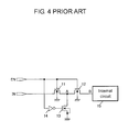
- FIG. 4 illustrates a conventional switch circuit.
- the switch circuit controls whether a positive or negative voltage input to an input terminal IN is transmitted or interrupted to an internal circuit 15 in response to a signal of a switch control terminal EN.
- a positive voltage VIN+ input from the input terminal IN is transmitted to a node B serving as an input terminal of the internal circuit 15 .
- the signal of the switch control terminal EN is set to a VDD voltage in an active state, to thereby turn ON NMOS transistors 11 and 12 . Therefore, the positive voltage VIN+ input from the input terminal IN is transmitted to the node B serving as the input of the internal circuit 15 .
- an NMOS transistor 13 is turned OFF, and hence the NMOS transistor 13 does not affect the voltage of the node B.
- the signal of the switch control terminal EN is set to a GND voltage in an inactive state.
- a drain of the NMOS transistor 11 has the voltage VIN+ and a gate thereof has the GND voltage, and hence the NMOS transistor 11 is turned OFF.
- the NMOS transistor 13 is turned ON so that a node A has the GND voltage.
- a drain and a gate of the NMOS transistor 12 have the GND voltage, and hence the NMOS transistor 12 is turned OFF. Therefore, the positive voltage VIN+ input from the input terminal IN is not transmitted to the node B serving as the input of the internal circuit 15 .
- a negative voltage VIN ⁇ input from the input terminal IN is not transmitted to the node B serving as the input of the internal circuit 15 .
- the signal of the switch control terminal EN is set to the GND voltage in the inactive state.
- the drain of the NMOS transistor 11 is applied with the negative voltage VIN ⁇ lower than the GND voltage input from the input terminal IN, and hence the NMOS transistor 11 becomes an ON state in the weak inversion region.
- the NMOS transistor 13 is turned ON, and hence the node A has the GND voltage rather than the input negative voltage VIN ⁇ .
- the drain and the gate of the NMOS transistor 12 have the GND voltage, and hence the NMOS transistor 12 is turned OFF. Therefore, the negative voltage VIN ⁇ input from the input terminal IN is not transmitted to the node B serving as the input of the internal circuit 15 .
- the conventional switch circuit can prevent the negative voltage from being transmitted to the input of the internal circuit 15 , thus preventing an erroneous operation of the internal circuit.
- VDD ⁇ VGS ⁇ VOV a voltage (VDD ⁇ VGS ⁇ VOV)
- VGS a threshold voltage (VGS>0 V) of the NMOS transistors 11 and 12
- VOV an overdrive voltage (VOV>0 V) necessary for reliably turning ON the NMOS transistors 11 and 12 .
- the active state signal of the switch control terminal EN needs to be a voltage equal to or higher than a voltage (VDD+VGS+VOV). Therefore, a booster circuit or a level shift circuit is necessary, which increases the circuit scale and the cost of products.
- a switch circuit including: a first NMOS transistor including a drain connected to an input terminal of a semiconductor device, a source connected to a first node, and a gate connected to a control terminal; a second NMOS transistor including a drain connected to the first node, a source connected to a second node, and a gate connected to the control terminal; a first PMOS transistor including a source connected to the input terminal of the semiconductor device, a drain connected to the first node, and a gate connected to the control terminal via an inverter; a second PMOS transistor including a source connected to the first node, a drain connected to the second node, and a gate connected to the control terminal via the inverter; and a third NMOS transistor including a source connected to a ground voltage, a drain connected to the first node, and a gate connected to the control terminal via the inverter, in which the second node is connected
- the switch circuit of the present invention even when a negative voltage is input from the input terminal, the negative voltage can be prevented from being transmitted to the input of the internal circuit, and further, a positive voltage up to a VDD voltage can be transmitted to the input of the internal circuit.
- FIG. 1 is a circuit diagram illustrating a switch circuit according to a first embodiment of the present invention
- FIG. 2 is a circuit diagram illustrating a switch circuit according to a second embodiment of the present invention.
- FIG. 3 is a circuit diagram illustrating an example of a level shift circuit according to the second embodiment of the present invention.
- FIG. 4 is a circuit diagram illustrating a conventional switch circuit.
- the switch circuit controls whether a positive or negative voltage input to an input terminal IN is transmitted or interrupted to an internal circuit 15 in response to a signal of a switch control terminal EN.
- FIG. 1 is a circuit diagram illustrating a switch circuit according to a first embodiment of the present invention.
- the switch circuit in the first embodiment includes NMOS transistors 11 , 12 , and 13 , PMOS transistors 16 and 17 , and an inverter 14 .
- the NMOS transistor 11 has a drain connected to the input terminal IN, a gate connected to the switch control terminal EN, a source connected to a drain of the NMOS transistor 12 , and a back gate connected to GND.
- the NMOS transistor 12 has a gate connected to the switch control terminal EN, a source connected to an input terminal (node B) of the internal circuit 15 , and a back gate connected to GND.
- the PMOS transistor 16 has a source connected to the input terminal IN, a gate connected to an output terminal of the inverter 14 , a drain connected to a source of the PMOS transistor 17 , and a back gate connected to VDD.
- the PMOS transistor 17 has a gate connected to the output terminal of the inverter 14 , a drain connected to the node B, and a back gate connected to VDD.
- the inverter 14 has an input terminal connected to the switch control terminal EN.
- the NMOS transistor 13 has a gate connected to the output terminal of the inverter 14 , a source grounded to GND, a drain connected to the source of the NMOS transistor 11 , to the drain of the NMOS transistor 12 , to the drain of the PMOS transistor 16 , and to the source of the PMOS transistor 17 , and a back gate connected to GND.
- the NMOS transistors 11 and 12 and the PMOS transistors 16 and 17 are controlled to be turned ON/OFF in response to a signal of the switch control terminal EN.
- the inverter 14 inverts an input signal of a VDD/GND voltage, and outputs the inverted signal.
- the NMOS transistor 13 is controlled to be turned ON when the NMOS transistors 11 and 12 and the PMOS transistors 16 and 17 are turned OFF.
- a signal of the GND voltage in an inactive state is input.
- the drain of the NMOS transistor 11 has the voltage VIN+ and the gate thereof has the GND voltage, and hence the NMOS transistor 11 is turned OFF.
- the source of the PMOS transistor 16 has the voltage VIN+ and the gate thereof has the VDD voltage, and hence the PMOS transistor 16 is turned OFF.
- the gate of the NMOS transistor 13 has the VDD voltage, and hence the NMOS transistor 13 is turned ON so that a node A has the GND voltage.
- the drain and the gate of the NMOS transistor 12 have the GND voltage, and hence the NMOS transistor 12 is turned OFF.
- the source of the PMOS transistor 17 has the GND voltage and the gate thereof has the VDD voltage, and hence the PMOS transistor 17 is turned OFF. Therefore, the positive voltage VIN+ input from the input terminal IN is not transmitted to the node B.
- the signal of the GND voltage in the inactive state is input.
- the drain of the NMOS transistor 11 has the negative voltage VIN ⁇ and the gate thereof has the GND voltage, and hence the NMOS transistor 11 becomes an ON state in the weak inversion region.
- the gate of the NMOS transistor 13 has the VDD voltage, and hence the NMOS transistor 13 is turned ON so that the node A has the GND voltage.
- the drain of the NMOS transistor 12 has the GND voltage and the gate thereof also has the GND voltage, and hence the NMOS transistor 12 is turned OFF.
- the gates of the PMOS transistors 16 and 17 have the VDD voltage, and hence the PMOS transistors 16 and 17 are turned OFF. Therefore, the negative voltage VIN ⁇ input from the input terminal IN is not transmitted to the node B.
- VDD represents a power supply voltage
- VGS represents a threshold voltage (VGS>0 V) of the NMOS transistors 11 and 12
- VOV represents an overdrive voltage (VOV>0 V) necessary for reliably turning ON the NMOS transistors 11 and 12 .
- the source of the PMOS transistor 16 has the VDD voltage and the gate thereof has the GND voltage, and hence the PMOS transistor 16 is turned ON so that the VDD voltage is transmitted to the drain.
- the PMOS transistor 16 is fully turned ON, and hence the drain voltage of the PMOS transistor 16 is dominant in the voltage of the node A. Therefore, the voltage of the node A becomes the VDD voltage.
- the switch circuit in this embodiment can transmit an input voltage in the range of from the GND voltage to the VDD voltage.
- FIG. 2 is a circuit diagram illustrating a switch circuit according to a second embodiment of the present invention.
- the switch circuit in the second embodiment includes a level shift circuit 18 in addition to the circuit of FIG. 1 .
- the level shift circuit 18 has a power supply terminal V connected to the input terminal IN, an output terminal O connected to the gate of the PMOS transistor 16 , and an input terminal I connected to the switch control terminal EN.
- the PMOS transistor 16 has a back gate connected to the input terminal IN.
- the level shift circuit 18 performs voltage conversion on a signal of the input terminal I based on a voltage of the power supply terminal V, and outputs the converted signal from the output terminal O.
- the level shift circuit 18 is configured to invert the logic between input and output.
- a signal of the input terminal I is the VDD voltage
- a signal of the GND voltage is output from the output terminal O.
- the signal of the input terminal I is the GND voltage
- a signal of the voltage of the power supply terminal V is output from the output terminal O.
- the back gate of the PMOS transistor 16 is connected to VDD, the back gate voltage becomes lower than a source voltage. Therefore, an unnecessary current flows from the input terminal IN to VDD via the PMOS transistor 16 (from source to back gate).
- the back gate and the source of the PMOS transistor 16 are connected to the input terminal IN, and hence there is no potential difference between the back gate and the source, and no current path to VDD exists.
- the gate of the PMOS transistor 16 has the voltage of the input terminal IN which is output from the output terminal O of the level shift circuit 18 . Therefore, the gate of the PMOS transistor 16 is applied with a voltage necessary for turning OFF the PMOS transistor 16 .
- FIG. 3 is an example of the level shift circuit configuration used in the switch circuit of the second embodiment.
- the level shift circuit only needs to have a simple and general configuration including PMOS transistors 21 and 22 and NMOS transistors 23 and 24 .
- the switch circuit in the second embodiment even when a voltage higher than the VDD voltage is applied from the input terminal IN when the switch is OFF, it is possible to prevent an unnecessary current from flowing to the input terminal IN, thus preventing the PMOS transistor 16 from being broken down.
Landscapes
- Engineering & Computer Science (AREA)
- Computer Hardware Design (AREA)
- Physics & Mathematics (AREA)
- Computing Systems (AREA)
- General Engineering & Computer Science (AREA)
- Mathematical Physics (AREA)
- Electronic Switches (AREA)
- Logic Circuits (AREA)
Applications Claiming Priority (3)
| Application Number | Priority Date | Filing Date | Title |
|---|---|---|---|
| JP2012044156A JP5845112B2 (ja) | 2012-02-29 | 2012-02-29 | スイッチ回路 |
| JP2012-044156 | 2012-02-29 | ||
| PCT/JP2013/051706 WO2013128997A1 (ja) | 2012-02-29 | 2013-01-28 | スイッチ回路 |
Related Parent Applications (1)
| Application Number | Title | Priority Date | Filing Date |
|---|---|---|---|
| PCT/JP2013/051706 Continuation WO2013128997A1 (ja) | 2012-02-29 | 2013-01-28 | スイッチ回路 |
Publications (2)
| Publication Number | Publication Date |
|---|---|
| US20140361825A1 US20140361825A1 (en) | 2014-12-11 |
| US9444451B2 true US9444451B2 (en) | 2016-09-13 |
Family
ID=49082201
Family Applications (1)
| Application Number | Title | Priority Date | Filing Date |
|---|---|---|---|
| US14/469,207 Active 2033-03-04 US9444451B2 (en) | 2012-02-29 | 2014-08-26 | Switch circuit |
Country Status (6)
| Country | Link |
|---|---|
| US (1) | US9444451B2 (ja) |
| JP (1) | JP5845112B2 (ja) |
| KR (1) | KR101716941B1 (ja) |
| CN (1) | CN104137418B (ja) |
| TW (2) | TW201340602A (ja) |
| WO (1) | WO2013128997A1 (ja) |
Cited By (1)
| Publication number | Priority date | Publication date | Assignee | Title |
|---|---|---|---|---|
| US20240072786A1 (en) * | 2022-08-23 | 2024-02-29 | Nexperia B.V. | Area efficient bidirectional switch with off state injection current control |
Families Citing this family (8)
| Publication number | Priority date | Publication date | Assignee | Title |
|---|---|---|---|---|
| US20150381160A1 (en) * | 2014-06-26 | 2015-12-31 | Infineon Technologies Ag | Robust multiplexer, and method for operating a robust multiplexer |
| JP2016136681A (ja) * | 2015-01-23 | 2016-07-28 | エスアイアイ・セミコンダクタ株式会社 | スイッチ回路 |
| US10236873B2 (en) * | 2015-03-17 | 2019-03-19 | Xilinx, Inc. | Analog switch having reduced gate-induced drain leakage |
| KR101638352B1 (ko) | 2015-04-24 | 2016-07-13 | 주식회사 지니틱스 | 코일에 연결된 출력단자를 플로팅되도록 하는 회로를 갖는 코일 구동 ic |
| EP3504676A4 (en) | 2016-08-26 | 2020-03-25 | Allstate Insurance Company | AUTOMATIC DETECTION AND REPAIR OF HAIL DAMAGE |
| JP7329411B2 (ja) * | 2019-10-18 | 2023-08-18 | エイブリック株式会社 | アナログスイッチ |
| TWI852168B (zh) * | 2022-11-16 | 2024-08-11 | 立積電子股份有限公司 | 開關裝置 |
| TWI865988B (zh) | 2022-12-14 | 2024-12-11 | 立積電子股份有限公司 | 開關裝置 |
Citations (8)
| Publication number | Priority date | Publication date | Assignee | Title |
|---|---|---|---|---|
| JPH01198823A (ja) | 1988-02-03 | 1989-08-10 | Nec Corp | 入力回路 |
| JPH01236731A (ja) | 1988-03-16 | 1989-09-21 | Nec Corp | 相補型アナログスイッチ |
| GB2319128A (en) | 1996-10-30 | 1998-05-13 | Motorola Gmbh | A CMOS transmission gate multiplexer with improved OFF isolation |
| US6400209B1 (en) * | 1999-08-05 | 2002-06-04 | Fujitsu Limited | Switch circuit with back gate voltage control and series regulator |
| JP2002527975A (ja) | 1998-10-09 | 2002-08-27 | ミツビシ・セミコンダクター・ヨーロッパ・ゲゼルシャフト・ミット・ベシュレンクテル・ハフツング | マルチプレクサ回路およびアナログデジタル変換器 |
| US6911860B1 (en) * | 2001-11-09 | 2005-06-28 | Altera Corporation | On/off reference voltage switch for multiple I/O standards |
| JP2010206779A (ja) | 2009-02-06 | 2010-09-16 | Seiko Instruments Inc | スイッチ回路 |
| US8810302B2 (en) * | 2009-12-30 | 2014-08-19 | Stmicroelectronics S.R.L. | Low voltage isolation switch, in particular for a transmission channel for ultrasound applications |
Family Cites Families (2)
| Publication number | Priority date | Publication date | Assignee | Title |
|---|---|---|---|---|
| JP5476198B2 (ja) * | 2010-04-19 | 2014-04-23 | ルネサスエレクトロニクス株式会社 | 高周波スイッチ回路 |
| CN102332901A (zh) * | 2011-08-15 | 2012-01-25 | 苏州佳世达电通有限公司 | 开关电路及显示装置 |
-
2012
- 2012-02-29 JP JP2012044156A patent/JP5845112B2/ja active Active
-
2013
- 2013-01-23 TW TW102102471A patent/TW201340602A/zh unknown
- 2013-01-23 TW TW105120564A patent/TWI575872B/zh active
- 2013-01-28 CN CN201380011008.1A patent/CN104137418B/zh active Active
- 2013-01-28 KR KR1020147023959A patent/KR101716941B1/ko active Active
- 2013-01-28 WO PCT/JP2013/051706 patent/WO2013128997A1/ja not_active Ceased
-
2014
- 2014-08-26 US US14/469,207 patent/US9444451B2/en active Active
Patent Citations (10)
| Publication number | Priority date | Publication date | Assignee | Title |
|---|---|---|---|---|
| JPH01198823A (ja) | 1988-02-03 | 1989-08-10 | Nec Corp | 入力回路 |
| US4985703A (en) | 1988-02-03 | 1991-01-15 | Nec Corporation | Analog multiplexer |
| JPH01236731A (ja) | 1988-03-16 | 1989-09-21 | Nec Corp | 相補型アナログスイッチ |
| GB2319128A (en) | 1996-10-30 | 1998-05-13 | Motorola Gmbh | A CMOS transmission gate multiplexer with improved OFF isolation |
| JP2002527975A (ja) | 1998-10-09 | 2002-08-27 | ミツビシ・セミコンダクター・ヨーロッパ・ゲゼルシャフト・ミット・ベシュレンクテル・ハフツング | マルチプレクサ回路およびアナログデジタル変換器 |
| US7031349B1 (en) | 1998-10-09 | 2006-04-18 | Mitsubishi Semiconductor Europe Gmbh | Multiplexer circuit and analogue-to-digital converter |
| US6400209B1 (en) * | 1999-08-05 | 2002-06-04 | Fujitsu Limited | Switch circuit with back gate voltage control and series regulator |
| US6911860B1 (en) * | 2001-11-09 | 2005-06-28 | Altera Corporation | On/off reference voltage switch for multiple I/O standards |
| JP2010206779A (ja) | 2009-02-06 | 2010-09-16 | Seiko Instruments Inc | スイッチ回路 |
| US8810302B2 (en) * | 2009-12-30 | 2014-08-19 | Stmicroelectronics S.R.L. | Low voltage isolation switch, in particular for a transmission channel for ultrasound applications |
Non-Patent Citations (1)
| Title |
|---|
| International Search Report of PCT/JP2013/051706 dated Feb. 19, 2013, 2 pages. |
Cited By (2)
| Publication number | Priority date | Publication date | Assignee | Title |
|---|---|---|---|---|
| US20240072786A1 (en) * | 2022-08-23 | 2024-02-29 | Nexperia B.V. | Area efficient bidirectional switch with off state injection current control |
| US12401357B2 (en) * | 2022-08-23 | 2025-08-26 | Nexperia B.V. | Area efficient bidirectional switch with off state injection current control |
Also Published As
| Publication number | Publication date |
|---|---|
| TWI575872B (zh) | 2017-03-21 |
| TW201637364A (zh) | 2016-10-16 |
| US20140361825A1 (en) | 2014-12-11 |
| TW201340602A (zh) | 2013-10-01 |
| KR101716941B1 (ko) | 2017-03-27 |
| CN104137418A (zh) | 2014-11-05 |
| JP5845112B2 (ja) | 2016-01-20 |
| JP2013183206A (ja) | 2013-09-12 |
| KR20140138138A (ko) | 2014-12-03 |
| WO2013128997A1 (ja) | 2013-09-06 |
| CN104137418B (zh) | 2017-06-16 |
Similar Documents
| Publication | Publication Date | Title |
|---|---|---|
| US9444451B2 (en) | Switch circuit | |
| US10116309B2 (en) | CMOS output circuit | |
| US20130222037A1 (en) | Voltage level shifter | |
| TW201830861A (zh) | 移位器 | |
| US8581639B2 (en) | Differential output circuit | |
| US7501874B2 (en) | Level shift circuit | |
| US10270449B2 (en) | High-voltage level shift circuit and drive apparatus | |
| JP5190335B2 (ja) | トレラントバッファ回路及びインターフェース | |
| US10355675B2 (en) | Input circuit | |
| US9660651B2 (en) | Level shift circuit | |
| US8513984B2 (en) | Buffer circuit having switch circuit capable of outputting two and more different high voltage potentials | |
| JP2006311201A (ja) | バッファ回路 | |
| US10382041B2 (en) | Buffer circuit | |
| US9571094B2 (en) | Switch circuit | |
| US20130063195A1 (en) | Digital input buffer | |
| KR20200070603A (ko) | 입출력 회로 및 이를 포함하는 전자 소자 | |
| US11177808B2 (en) | Semiconductor device | |
| KR20200114583A (ko) | 전압 온-오프 검출기 및 이를 포함하는 전자 소자 | |
| JP2013021498A (ja) | Cmos論理集積回路 | |
| JP2018142894A (ja) | 出力バッファ及び半導体装置 | |
| JP2014168131A (ja) | Cmosインバータ回路 | |
| TWM517481U (zh) | 電壓位準轉換器 | |
| US20150091619A1 (en) | Semiconductor apparatus |
Legal Events
| Date | Code | Title | Description |
|---|---|---|---|
| AS | Assignment |
Owner name: SEIKO INSTRUMENTS INC., JAPAN Free format text: ASSIGNMENT OF ASSIGNORS INTEREST;ASSIGNOR:SATO, YUTAKA;REEL/FRAME:033616/0227 Effective date: 20140807 |
|
| AS | Assignment |
Owner name: SII SEMICONDUCTOR CORPORATION ., JAPAN Free format text: ASSIGNMENT OF ASSIGNORS INTEREST;ASSIGNOR:SEIKO INSTRUMENTS INC;REEL/FRAME:037783/0166 Effective date: 20160209 |
|
| AS | Assignment |
Owner name: SII SEMICONDUCTOR CORPORATION, JAPAN Free format text: CORRECTIVE ASSIGNMENT TO CORRECT THE EXECUTION DATE PREVIOUSLY RECORDED AT REEL: 037783 FRAME: 0166. ASSIGNOR(S) HEREBY CONFIRMS THE ASSIGNMENT;ASSIGNOR:SEIKO INSTRUMENTS INC;REEL/FRAME:037903/0928 Effective date: 20160201 |
|
| STCF | Information on status: patent grant |
Free format text: PATENTED CASE |
|
| AS | Assignment |
Owner name: ABLIC INC., JAPAN Free format text: CHANGE OF NAME;ASSIGNOR:SII SEMICONDUCTOR CORPORATION;REEL/FRAME:045567/0927 Effective date: 20180105 |
|
| MAFP | Maintenance fee payment |
Free format text: PAYMENT OF MAINTENANCE FEE, 4TH YEAR, LARGE ENTITY (ORIGINAL EVENT CODE: M1551); ENTITY STATUS OF PATENT OWNER: LARGE ENTITY Year of fee payment: 4 |
|
| AS | Assignment |
Owner name: ABLIC INC., JAPAN Free format text: CHANGE OF ADDRESS;ASSIGNOR:ABLIC INC.;REEL/FRAME:064021/0575 Effective date: 20230424 |
|
| MAFP | Maintenance fee payment |
Free format text: PAYMENT OF MAINTENANCE FEE, 8TH YEAR, LARGE ENTITY (ORIGINAL EVENT CODE: M1552); ENTITY STATUS OF PATENT OWNER: LARGE ENTITY Year of fee payment: 8 |