US9391231B2 - Method for preparing a thin layer of an absorber made of copper, zinc and tin sulfide(s), annealed thin layer and photovoltaic device thus obtained - Google Patents
Method for preparing a thin layer of an absorber made of copper, zinc and tin sulfide(s), annealed thin layer and photovoltaic device thus obtained Download PDFInfo
- Publication number
- US9391231B2 US9391231B2 US14/758,314 US201314758314A US9391231B2 US 9391231 B2 US9391231 B2 US 9391231B2 US 201314758314 A US201314758314 A US 201314758314A US 9391231 B2 US9391231 B2 US 9391231B2
- Authority
- US
- United States
- Prior art keywords
- layer
- annealing
- substrate
- czts
- alcoholic
- Prior art date
- Legal status (The legal status is an assumption and is not a legal conclusion. Google has not performed a legal analysis and makes no representation as to the accuracy of the status listed.)
- Active
Links
- 239000010949 copper Substances 0.000 title claims abstract description 67
- 239000011701 zinc Substances 0.000 title claims abstract description 64
- 238000000034 method Methods 0.000 title claims abstract description 63
- 229910052802 copper Inorganic materials 0.000 title claims abstract description 53
- 239000011135 tin Substances 0.000 title claims abstract description 53
- 229910052725 zinc Inorganic materials 0.000 title claims abstract description 49
- 239000006096 absorbing agent Substances 0.000 title claims abstract description 38
- 229910052718 tin Inorganic materials 0.000 title claims abstract description 37
- UCKMPCXJQFINFW-UHFFFAOYSA-N Sulphide Chemical compound [S-2] UCKMPCXJQFINFW-UHFFFAOYSA-N 0.000 title claims abstract description 21
- RYGMFSIKBFXOCR-UHFFFAOYSA-N Copper Chemical compound [Cu] RYGMFSIKBFXOCR-UHFFFAOYSA-N 0.000 title claims abstract description 17
- HCHKCACWOHOZIP-UHFFFAOYSA-N Zinc Chemical compound [Zn] HCHKCACWOHOZIP-UHFFFAOYSA-N 0.000 title claims abstract description 16
- ATJFFYVFTNAWJD-UHFFFAOYSA-N Tin Chemical compound [Sn] ATJFFYVFTNAWJD-UHFFFAOYSA-N 0.000 title claims description 10
- 238000000137 annealing Methods 0.000 claims abstract description 115
- 239000000758 substrate Substances 0.000 claims abstract description 72
- 239000002245 particle Substances 0.000 claims abstract description 39
- 239000000463 material Substances 0.000 claims abstract description 29
- 239000000203 mixture Substances 0.000 claims abstract description 28
- ZOKXTWBITQBERF-UHFFFAOYSA-N Molybdenum Chemical compound [Mo] ZOKXTWBITQBERF-UHFFFAOYSA-N 0.000 claims abstract description 17
- 229910052750 molybdenum Inorganic materials 0.000 claims abstract description 17
- 239000011733 molybdenum Substances 0.000 claims abstract description 17
- AFNRRBXCCXDRPS-UHFFFAOYSA-N tin(ii) sulfide Chemical compound [Sn]=S AFNRRBXCCXDRPS-UHFFFAOYSA-N 0.000 claims abstract description 6
- IJGRMHOSHXDMSA-UHFFFAOYSA-N Atomic nitrogen Chemical compound N#N IJGRMHOSHXDMSA-UHFFFAOYSA-N 0.000 claims description 52
- 239000012298 atmosphere Substances 0.000 claims description 51
- WEVYAHXRMPXWCK-UHFFFAOYSA-N Acetonitrile Chemical compound CC#N WEVYAHXRMPXWCK-UHFFFAOYSA-N 0.000 claims description 48
- 238000001246 colloidal dispersion Methods 0.000 claims description 45
- 229910052751 metal Inorganic materials 0.000 claims description 32
- 239000002184 metal Substances 0.000 claims description 32
- 239000000243 solution Substances 0.000 claims description 31
- 239000002105 nanoparticle Substances 0.000 claims description 30
- LFQSCWFLJHTTHZ-UHFFFAOYSA-N Ethanol Chemical compound CCO LFQSCWFLJHTTHZ-UHFFFAOYSA-N 0.000 claims description 29
- 238000004519 manufacturing process Methods 0.000 claims description 29
- 239000006185 dispersion Substances 0.000 claims description 28
- 238000010438 heat treatment Methods 0.000 claims description 28
- 229910052757 nitrogen Inorganic materials 0.000 claims description 25
- XLYOFNOQVPJJNP-UHFFFAOYSA-N water Substances O XLYOFNOQVPJJNP-UHFFFAOYSA-N 0.000 claims description 25
- 239000002243 precursor Substances 0.000 claims description 24
- XKRFYHLGVUSROY-UHFFFAOYSA-N Argon Chemical compound [Ar] XKRFYHLGVUSROY-UHFFFAOYSA-N 0.000 claims description 22
- 239000002904 solvent Substances 0.000 claims description 22
- 239000011521 glass Substances 0.000 claims description 21
- 150000001875 compounds Chemical class 0.000 claims description 20
- 230000007935 neutral effect Effects 0.000 claims description 20
- 239000007787 solid Substances 0.000 claims description 20
- 150000002739 metals Chemical class 0.000 claims description 19
- 230000001476 alcoholic effect Effects 0.000 claims description 17
- 239000000084 colloidal system Substances 0.000 claims description 16
- 239000007788 liquid Substances 0.000 claims description 14
- 239000007789 gas Substances 0.000 claims description 13
- 239000002002 slurry Substances 0.000 claims description 12
- 150000004763 sulfides Chemical class 0.000 claims description 12
- 229910052786 argon Inorganic materials 0.000 claims description 11
- 239000002244 precipitate Substances 0.000 claims description 10
- 238000004140 cleaning Methods 0.000 claims description 8
- 238000010521 absorption reaction Methods 0.000 claims description 7
- 229910052976 metal sulfide Inorganic materials 0.000 claims description 7
- 238000002360 preparation method Methods 0.000 claims description 7
- 229910002475 Cu2ZnSnS4 Inorganic materials 0.000 claims description 6
- 238000005119 centrifugation Methods 0.000 claims description 6
- 239000013078 crystal Substances 0.000 claims description 6
- 239000006228 supernatant Substances 0.000 claims description 5
- 239000011592 zinc chloride Substances 0.000 claims description 5
- JIAARYAFYJHUJI-UHFFFAOYSA-L zinc dichloride Chemical compound [Cl-].[Cl-].[Zn+2] JIAARYAFYJHUJI-UHFFFAOYSA-L 0.000 claims description 5
- 229910000831 Steel Inorganic materials 0.000 claims description 4
- 239000002253 acid Substances 0.000 claims description 4
- 238000002156 mixing Methods 0.000 claims description 4
- 239000010959 steel Substances 0.000 claims description 4
- 229910021627 Tin(IV) chloride Inorganic materials 0.000 claims description 3
- 239000007864 aqueous solution Substances 0.000 claims description 3
- 239000012159 carrier gas Substances 0.000 claims description 3
- 239000004065 semiconductor Substances 0.000 claims description 3
- HPGGPRDJHPYFRM-UHFFFAOYSA-J tin(iv) chloride Chemical compound Cl[Sn](Cl)(Cl)Cl HPGGPRDJHPYFRM-UHFFFAOYSA-J 0.000 claims description 3
- 229910021592 Copper(II) chloride Inorganic materials 0.000 claims description 2
- ORTQZVOHEJQUHG-UHFFFAOYSA-L copper(II) chloride Chemical compound Cl[Cu]Cl ORTQZVOHEJQUHG-UHFFFAOYSA-L 0.000 claims description 2
- 238000002425 crystallisation Methods 0.000 claims description 2
- 230000008025 crystallization Effects 0.000 claims description 2
- 150000004820 halides Chemical class 0.000 claims description 2
- 229910021626 Tin(II) chloride Inorganic materials 0.000 claims 1
- 159000000011 group IA salts Chemical class 0.000 claims 1
- 230000007547 defect Effects 0.000 abstract description 8
- 239000012071 phase Substances 0.000 description 40
- 238000002441 X-ray diffraction Methods 0.000 description 24
- 238000000151 deposition Methods 0.000 description 22
- 230000000052 comparative effect Effects 0.000 description 20
- 239000010408 film Substances 0.000 description 19
- 230000008021 deposition Effects 0.000 description 16
- 239000012299 nitrogen atmosphere Substances 0.000 description 13
- 238000002149 energy-dispersive X-ray emission spectroscopy Methods 0.000 description 11
- 238000004458 analytical method Methods 0.000 description 9
- 238000013507 mapping Methods 0.000 description 8
- VEXZGXHMUGYJMC-UHFFFAOYSA-N Hydrochloric acid Chemical compound Cl VEXZGXHMUGYJMC-UHFFFAOYSA-N 0.000 description 7
- 238000006243 chemical reaction Methods 0.000 description 7
- 239000000976 ink Substances 0.000 description 7
- 239000003446 ligand Substances 0.000 description 7
- 239000000843 powder Substances 0.000 description 7
- OKKJLVBELUTLKV-UHFFFAOYSA-N Methanol Chemical compound OC OKKJLVBELUTLKV-UHFFFAOYSA-N 0.000 description 6
- 229910052980 cadmium sulfide Inorganic materials 0.000 description 6
- 238000001816 cooling Methods 0.000 description 6
- 238000005507 spraying Methods 0.000 description 6
- 239000000126 substance Substances 0.000 description 6
- 231100000331 toxic Toxicity 0.000 description 6
- 230000002588 toxic effect Effects 0.000 description 6
- PXHVJJICTQNCMI-UHFFFAOYSA-N Nickel Chemical compound [Ni] PXHVJJICTQNCMI-UHFFFAOYSA-N 0.000 description 5
- NINIDFKCEFEMDL-UHFFFAOYSA-N Sulfur Chemical compound [S] NINIDFKCEFEMDL-UHFFFAOYSA-N 0.000 description 5
- 239000005864 Sulphur Substances 0.000 description 5
- 238000009835 boiling Methods 0.000 description 5
- 238000004626 scanning electron microscopy Methods 0.000 description 5
- 239000012535 impurity Substances 0.000 description 4
- 239000013110 organic ligand Substances 0.000 description 4
- 230000003647 oxidation Effects 0.000 description 4
- 238000007254 oxidation reaction Methods 0.000 description 4
- 230000005855 radiation Effects 0.000 description 4
- 230000006798 recombination Effects 0.000 description 4
- 238000005215 recombination Methods 0.000 description 4
- 150000003839 salts Chemical class 0.000 description 4
- BQCADISMDOOEFD-UHFFFAOYSA-N Silver Chemical compound [Ag] BQCADISMDOOEFD-UHFFFAOYSA-N 0.000 description 3
- 229910007609 Zn—S Inorganic materials 0.000 description 3
- 239000002800 charge carrier Substances 0.000 description 3
- 238000000354 decomposition reaction Methods 0.000 description 3
- 239000004571 lime Substances 0.000 description 3
- 239000011159 matrix material Substances 0.000 description 3
- 238000005259 measurement Methods 0.000 description 3
- 229910052709 silver Inorganic materials 0.000 description 3
- 239000004332 silver Substances 0.000 description 3
- 229910052717 sulfur Inorganic materials 0.000 description 3
- 230000003746 surface roughness Effects 0.000 description 3
- 239000010409 thin film Substances 0.000 description 3
- 238000004627 transmission electron microscopy Methods 0.000 description 3
- 238000001771 vacuum deposition Methods 0.000 description 3
- XLOMVQKBTHCTTD-UHFFFAOYSA-N zinc oxide Inorganic materials [Zn]=O XLOMVQKBTHCTTD-UHFFFAOYSA-N 0.000 description 3
- 239000011787 zinc oxide Substances 0.000 description 3
- GNFTZDOKVXKIBK-UHFFFAOYSA-N 3-(2-methoxyethoxy)benzohydrazide Chemical compound COCCOC1=CC=CC(C(=O)NN)=C1 GNFTZDOKVXKIBK-UHFFFAOYSA-N 0.000 description 2
- QGZKDVFQNNGYKY-UHFFFAOYSA-N Ammonia Chemical compound N QGZKDVFQNNGYKY-UHFFFAOYSA-N 0.000 description 2
- OKTJSMMVPCPJKN-UHFFFAOYSA-N Carbon Chemical compound [C] OKTJSMMVPCPJKN-UHFFFAOYSA-N 0.000 description 2
- 229910004613 CdTe Inorganic materials 0.000 description 2
- 229910021591 Copper(I) chloride Inorganic materials 0.000 description 2
- -1 Cu—S Chemical class 0.000 description 2
- OAKJQQAXSVQMHS-UHFFFAOYSA-N Hydrazine Chemical compound NN OAKJQQAXSVQMHS-UHFFFAOYSA-N 0.000 description 2
- FAPWRFPIFSIZLT-UHFFFAOYSA-M Sodium chloride Chemical compound [Na+].[Cl-] FAPWRFPIFSIZLT-UHFFFAOYSA-M 0.000 description 2
- 229910007610 Zn—Sn Inorganic materials 0.000 description 2
- 229910045601 alloy Inorganic materials 0.000 description 2
- 239000000956 alloy Substances 0.000 description 2
- 239000004411 aluminium Substances 0.000 description 2
- 229910052782 aluminium Inorganic materials 0.000 description 2
- XAGFODPZIPBFFR-UHFFFAOYSA-N aluminium Chemical compound [Al] XAGFODPZIPBFFR-UHFFFAOYSA-N 0.000 description 2
- 239000003125 aqueous solvent Substances 0.000 description 2
- 239000006227 byproduct Substances 0.000 description 2
- 150000001768 cations Chemical class 0.000 description 2
- 238000012512 characterization method Methods 0.000 description 2
- 238000000224 chemical solution deposition Methods 0.000 description 2
- OXBLHERUFWYNTN-UHFFFAOYSA-M copper(I) chloride Chemical class [Cu]Cl OXBLHERUFWYNTN-UHFFFAOYSA-M 0.000 description 2
- 230000002950 deficient Effects 0.000 description 2
- 239000008367 deionised water Substances 0.000 description 2
- 229910021641 deionized water Inorganic materials 0.000 description 2
- 238000001704 evaporation Methods 0.000 description 2
- 230000008020 evaporation Effects 0.000 description 2
- 239000010931 gold Substances 0.000 description 2
- 230000007062 hydrolysis Effects 0.000 description 2
- 238000006460 hydrolysis reaction Methods 0.000 description 2
- 229910052738 indium Inorganic materials 0.000 description 2
- APFVFJFRJDLVQX-UHFFFAOYSA-N indium atom Chemical compound [In] APFVFJFRJDLVQX-UHFFFAOYSA-N 0.000 description 2
- 239000006193 liquid solution Substances 0.000 description 2
- 229910001510 metal chloride Inorganic materials 0.000 description 2
- 239000011859 microparticle Substances 0.000 description 2
- 229910052759 nickel Inorganic materials 0.000 description 2
- 231100000252 nontoxic Toxicity 0.000 description 2
- 230000003000 nontoxic effect Effects 0.000 description 2
- 229910052760 oxygen Inorganic materials 0.000 description 2
- BDERNNFJNOPAEC-UHFFFAOYSA-N propan-1-ol Chemical compound CCCO BDERNNFJNOPAEC-UHFFFAOYSA-N 0.000 description 2
- 229910052711 selenium Inorganic materials 0.000 description 2
- 229910052708 sodium Inorganic materials 0.000 description 2
- 239000011734 sodium Substances 0.000 description 2
- 238000010345 tape casting Methods 0.000 description 2
- 238000012360 testing method Methods 0.000 description 2
- DZXKSFDSPBRJPS-UHFFFAOYSA-N tin(2+);sulfide Chemical compound [S-2].[Sn+2] DZXKSFDSPBRJPS-UHFFFAOYSA-N 0.000 description 2
- KHMOASUYFVRATF-UHFFFAOYSA-J tin(4+);tetrachloride;pentahydrate Chemical class O.O.O.O.O.Cl[Sn](Cl)(Cl)Cl KHMOASUYFVRATF-UHFFFAOYSA-J 0.000 description 2
- 241001206158 Blepsias cirrhosus Species 0.000 description 1
- FGUUSXIOTUKUDN-IBGZPJMESA-N C1(=CC=CC=C1)N1C2=C(NC([C@H](C1)NC=1OC(=NN=1)C1=CC=CC=C1)=O)C=CC=C2 Chemical compound C1(=CC=CC=C1)N1C2=C(NC([C@H](C1)NC=1OC(=NN=1)C1=CC=CC=C1)=O)C=CC=C2 FGUUSXIOTUKUDN-IBGZPJMESA-N 0.000 description 1
- VEXZGXHMUGYJMC-UHFFFAOYSA-M Chloride anion Chemical compound [Cl-] VEXZGXHMUGYJMC-UHFFFAOYSA-M 0.000 description 1
- DGAQECJNVWCQMB-PUAWFVPOSA-M Ilexoside XXIX Chemical compound C[C@@H]1CC[C@@]2(CC[C@@]3(C(=CC[C@H]4[C@]3(CC[C@@H]5[C@@]4(CC[C@@H](C5(C)C)OS(=O)(=O)[O-])C)C)[C@@H]2[C@]1(C)O)C)C(=O)O[C@H]6[C@@H]([C@H]([C@@H]([C@H](O6)CO)O)O)O.[Na+] DGAQECJNVWCQMB-PUAWFVPOSA-M 0.000 description 1
- 229910018828 PO3H2 Inorganic materials 0.000 description 1
- NBIIXXVUZAFLBC-UHFFFAOYSA-N Phosphoric acid Chemical group OP(O)(O)=O NBIIXXVUZAFLBC-UHFFFAOYSA-N 0.000 description 1
- XUIMIQQOPSSXEZ-UHFFFAOYSA-N Silicon Chemical compound [Si] XUIMIQQOPSSXEZ-UHFFFAOYSA-N 0.000 description 1
- 238000000441 X-ray spectroscopy Methods 0.000 description 1
- 239000011358 absorbing material Substances 0.000 description 1
- 239000000654 additive Substances 0.000 description 1
- 238000004220 aggregation Methods 0.000 description 1
- 230000002776 aggregation Effects 0.000 description 1
- JYMITAMFTJDTAE-UHFFFAOYSA-N aluminum zinc oxygen(2-) Chemical compound [O-2].[Al+3].[Zn+2] JYMITAMFTJDTAE-UHFFFAOYSA-N 0.000 description 1
- 150000001408 amides Chemical class 0.000 description 1
- 150000001412 amines Chemical class 0.000 description 1
- 229910021529 ammonia Inorganic materials 0.000 description 1
- QVGXLLKOCUKJST-UHFFFAOYSA-N atomic oxygen Chemical compound [O] QVGXLLKOCUKJST-UHFFFAOYSA-N 0.000 description 1
- 239000011230 binding agent Substances 0.000 description 1
- 230000015572 biosynthetic process Effects 0.000 description 1
- 239000002981 blocking agent Substances 0.000 description 1
- 239000005388 borosilicate glass Substances 0.000 description 1
- 229910052793 cadmium Inorganic materials 0.000 description 1
- CJOBVZJTOIVNNF-UHFFFAOYSA-N cadmium sulfide Chemical compound [Cd]=S CJOBVZJTOIVNNF-UHFFFAOYSA-N 0.000 description 1
- 229910052799 carbon Inorganic materials 0.000 description 1
- 150000004770 chalcogenides Chemical class 0.000 description 1
- 238000005234 chemical deposition Methods 0.000 description 1
- 239000003795 chemical substances by application Substances 0.000 description 1
- 230000000536 complexating effect Effects 0.000 description 1
- 239000004020 conductor Substances 0.000 description 1
- 238000011109 contamination Methods 0.000 description 1
- 230000000593 degrading effect Effects 0.000 description 1
- 238000000280 densification Methods 0.000 description 1
- 238000001035 drying Methods 0.000 description 1
- 230000000694 effects Effects 0.000 description 1
- 238000004070 electrodeposition Methods 0.000 description 1
- PCHJSUWPFVWCPO-UHFFFAOYSA-N gold Chemical compound [Au] PCHJSUWPFVWCPO-UHFFFAOYSA-N 0.000 description 1
- 229910052737 gold Inorganic materials 0.000 description 1
- 229910002804 graphite Inorganic materials 0.000 description 1
- 239000010439 graphite Substances 0.000 description 1
- 229910003437 indium oxide Inorganic materials 0.000 description 1
- PJXISJQVUVHSOJ-UHFFFAOYSA-N indium(iii) oxide Chemical compound [O-2].[O-2].[O-2].[In+3].[In+3] PJXISJQVUVHSOJ-UHFFFAOYSA-N 0.000 description 1
- AMGQUBHHOARCQH-UHFFFAOYSA-N indium;oxotin Chemical compound [In].[Sn]=O AMGQUBHHOARCQH-UHFFFAOYSA-N 0.000 description 1
- 230000003993 interaction Effects 0.000 description 1
- 239000007791 liquid phase Substances 0.000 description 1
- 231100000956 nontoxicity Toxicity 0.000 description 1
- 231100000926 not very toxic Toxicity 0.000 description 1
- 150000007524 organic acids Chemical group 0.000 description 1
- 239000001301 oxygen Substances 0.000 description 1
- 239000003973 paint Substances 0.000 description 1
- 238000002161 passivation Methods 0.000 description 1
- 238000009304 pastoral farming Methods 0.000 description 1
- 239000011148 porous material Substances 0.000 description 1
- XAEFZNCEHLXOMS-UHFFFAOYSA-M potassium benzoate Chemical compound [K+].[O-]C(=O)C1=CC=CC=C1 XAEFZNCEHLXOMS-UHFFFAOYSA-M 0.000 description 1
- NNFCIKHAZHQZJG-UHFFFAOYSA-N potassium cyanide Chemical compound [K+].N#[C-] NNFCIKHAZHQZJG-UHFFFAOYSA-N 0.000 description 1
- 230000001737 promoting effect Effects 0.000 description 1
- 230000001172 regenerating effect Effects 0.000 description 1
- 230000000630 rising effect Effects 0.000 description 1
- 239000000523 sample Substances 0.000 description 1
- 238000001878 scanning electron micrograph Methods 0.000 description 1
- 238000005204 segregation Methods 0.000 description 1
- SPVXKVOXSXTJOY-UHFFFAOYSA-N selane Chemical compound [SeH2] SPVXKVOXSXTJOY-UHFFFAOYSA-N 0.000 description 1
- 229910000058 selane Inorganic materials 0.000 description 1
- JPUIEYBUBJBWQJ-UHFFFAOYSA-N selanylidene(sulfanylidene)tin Chemical compound S=[Sn]=[Se] JPUIEYBUBJBWQJ-UHFFFAOYSA-N 0.000 description 1
- 238000000926 separation method Methods 0.000 description 1
- 229910052710 silicon Inorganic materials 0.000 description 1
- 239000010703 silicon Substances 0.000 description 1
- 239000011780 sodium chloride Substances 0.000 description 1
- HYHCSLBZRBJJCH-UHFFFAOYSA-M sodium hydrosulfide Chemical compound [Na+].[SH-] HYHCSLBZRBJJCH-UHFFFAOYSA-M 0.000 description 1
- 238000003980 solgel method Methods 0.000 description 1
- 238000004528 spin coating Methods 0.000 description 1
- 239000007921 spray Substances 0.000 description 1
- 238000004544 sputter deposition Methods 0.000 description 1
- 238000010561 standard procedure Methods 0.000 description 1
- 239000007858 starting material Substances 0.000 description 1
- 239000004094 surface-active agent Substances 0.000 description 1
- 239000000725 suspension Substances 0.000 description 1
- JBQYATWDVHIOAR-UHFFFAOYSA-N tellanylidenegermanium Chemical compound [Te]=[Ge] JBQYATWDVHIOAR-UHFFFAOYSA-N 0.000 description 1
- 229910052714 tellurium Inorganic materials 0.000 description 1
- 125000001391 thioamide group Chemical group 0.000 description 1
- 150000003573 thiols Chemical class 0.000 description 1
Images


Classifications
-
- H—ELECTRICITY
- H01—ELECTRIC ELEMENTS
- H01L—SEMICONDUCTOR DEVICES NOT COVERED BY CLASS H10
- H01L31/00—Semiconductor devices sensitive to infrared radiation, light, electromagnetic radiation of shorter wavelength or corpuscular radiation and specially adapted either for the conversion of the energy of such radiation into electrical energy or for the control of electrical energy by such radiation; Processes or apparatus specially adapted for the manufacture or treatment thereof or of parts thereof; Details thereof
- H01L31/18—Processes or apparatus specially adapted for the manufacture or treatment of these devices or of parts thereof
- H01L31/186—Particular post-treatment for the devices, e.g. annealing, impurity gettering, short-circuit elimination, recrystallisation
- H01L31/1864—Annealing
-
- C—CHEMISTRY; METALLURGY
- C23—COATING METALLIC MATERIAL; COATING MATERIAL WITH METALLIC MATERIAL; CHEMICAL SURFACE TREATMENT; DIFFUSION TREATMENT OF METALLIC MATERIAL; COATING BY VACUUM EVAPORATION, BY SPUTTERING, BY ION IMPLANTATION OR BY CHEMICAL VAPOUR DEPOSITION, IN GENERAL; INHIBITING CORROSION OF METALLIC MATERIAL OR INCRUSTATION IN GENERAL
- C23C—COATING METALLIC MATERIAL; COATING MATERIAL WITH METALLIC MATERIAL; SURFACE TREATMENT OF METALLIC MATERIAL BY DIFFUSION INTO THE SURFACE, BY CHEMICAL CONVERSION OR SUBSTITUTION; COATING BY VACUUM EVAPORATION, BY SPUTTERING, BY ION IMPLANTATION OR BY CHEMICAL VAPOUR DEPOSITION, IN GENERAL
- C23C18/00—Chemical coating by decomposition of either liquid compounds or solutions of the coating forming compounds, without leaving reaction products of surface material in the coating; Contact plating
- C23C18/02—Chemical coating by decomposition of either liquid compounds or solutions of the coating forming compounds, without leaving reaction products of surface material in the coating; Contact plating by thermal decomposition
- C23C18/12—Chemical coating by decomposition of either liquid compounds or solutions of the coating forming compounds, without leaving reaction products of surface material in the coating; Contact plating by thermal decomposition characterised by the deposition of inorganic material other than metallic material
- C23C18/1204—Chemical coating by decomposition of either liquid compounds or solutions of the coating forming compounds, without leaving reaction products of surface material in the coating; Contact plating by thermal decomposition characterised by the deposition of inorganic material other than metallic material inorganic material, e.g. non-oxide and non-metallic such as sulfides, nitrides based compounds
-
- C—CHEMISTRY; METALLURGY
- C23—COATING METALLIC MATERIAL; COATING MATERIAL WITH METALLIC MATERIAL; CHEMICAL SURFACE TREATMENT; DIFFUSION TREATMENT OF METALLIC MATERIAL; COATING BY VACUUM EVAPORATION, BY SPUTTERING, BY ION IMPLANTATION OR BY CHEMICAL VAPOUR DEPOSITION, IN GENERAL; INHIBITING CORROSION OF METALLIC MATERIAL OR INCRUSTATION IN GENERAL
- C23C—COATING METALLIC MATERIAL; COATING MATERIAL WITH METALLIC MATERIAL; SURFACE TREATMENT OF METALLIC MATERIAL BY DIFFUSION INTO THE SURFACE, BY CHEMICAL CONVERSION OR SUBSTITUTION; COATING BY VACUUM EVAPORATION, BY SPUTTERING, BY ION IMPLANTATION OR BY CHEMICAL VAPOUR DEPOSITION, IN GENERAL
- C23C20/00—Chemical coating by decomposition of either solid compounds or suspensions of the coating forming compounds, without leaving reaction products of surface material in the coating
-
- C—CHEMISTRY; METALLURGY
- C23—COATING METALLIC MATERIAL; COATING MATERIAL WITH METALLIC MATERIAL; CHEMICAL SURFACE TREATMENT; DIFFUSION TREATMENT OF METALLIC MATERIAL; COATING BY VACUUM EVAPORATION, BY SPUTTERING, BY ION IMPLANTATION OR BY CHEMICAL VAPOUR DEPOSITION, IN GENERAL; INHIBITING CORROSION OF METALLIC MATERIAL OR INCRUSTATION IN GENERAL
- C23C—COATING METALLIC MATERIAL; COATING MATERIAL WITH METALLIC MATERIAL; SURFACE TREATMENT OF METALLIC MATERIAL BY DIFFUSION INTO THE SURFACE, BY CHEMICAL CONVERSION OR SUBSTITUTION; COATING BY VACUUM EVAPORATION, BY SPUTTERING, BY ION IMPLANTATION OR BY CHEMICAL VAPOUR DEPOSITION, IN GENERAL
- C23C28/00—Coating for obtaining at least two superposed coatings either by methods not provided for in a single one of groups C23C2/00 - C23C26/00 or by combinations of methods provided for in subclasses C23C and C25C or C25D
- C23C28/04—Coating for obtaining at least two superposed coatings either by methods not provided for in a single one of groups C23C2/00 - C23C26/00 or by combinations of methods provided for in subclasses C23C and C25C or C25D only coatings of inorganic non-metallic material
- C23C28/042—Coating for obtaining at least two superposed coatings either by methods not provided for in a single one of groups C23C2/00 - C23C26/00 or by combinations of methods provided for in subclasses C23C and C25C or C25D only coatings of inorganic non-metallic material including a refractory ceramic layer, e.g. refractory metal oxides, ZrO2, rare earth oxides
-
- H—ELECTRICITY
- H01—ELECTRIC ELEMENTS
- H01L—SEMICONDUCTOR DEVICES NOT COVERED BY CLASS H10
- H01L21/00—Processes or apparatus adapted for the manufacture or treatment of semiconductor or solid state devices or of parts thereof
- H01L21/02—Manufacture or treatment of semiconductor devices or of parts thereof
- H01L21/02104—Forming layers
- H01L21/02365—Forming inorganic semiconducting materials on a substrate
- H01L21/02436—Intermediate layers between substrates and deposited layers
- H01L21/02439—Materials
- H01L21/02491—Conductive materials
-
- H—ELECTRICITY
- H01—ELECTRIC ELEMENTS
- H01L—SEMICONDUCTOR DEVICES NOT COVERED BY CLASS H10
- H01L21/00—Processes or apparatus adapted for the manufacture or treatment of semiconductor or solid state devices or of parts thereof
- H01L21/02—Manufacture or treatment of semiconductor devices or of parts thereof
- H01L21/02104—Forming layers
- H01L21/02365—Forming inorganic semiconducting materials on a substrate
- H01L21/02518—Deposited layers
- H01L21/02521—Materials
- H01L21/02551—Group 12/16 materials
- H01L21/02557—Sulfides
-
- H—ELECTRICITY
- H01—ELECTRIC ELEMENTS
- H01L—SEMICONDUCTOR DEVICES NOT COVERED BY CLASS H10
- H01L21/00—Processes or apparatus adapted for the manufacture or treatment of semiconductor or solid state devices or of parts thereof
- H01L21/02—Manufacture or treatment of semiconductor devices or of parts thereof
- H01L21/02104—Forming layers
- H01L21/02365—Forming inorganic semiconducting materials on a substrate
- H01L21/02518—Deposited layers
- H01L21/02521—Materials
- H01L21/02568—Chalcogenide semiconducting materials not being oxides, e.g. ternary compounds
-
- H—ELECTRICITY
- H01—ELECTRIC ELEMENTS
- H01L—SEMICONDUCTOR DEVICES NOT COVERED BY CLASS H10
- H01L21/00—Processes or apparatus adapted for the manufacture or treatment of semiconductor or solid state devices or of parts thereof
- H01L21/02—Manufacture or treatment of semiconductor devices or of parts thereof
- H01L21/02104—Forming layers
- H01L21/02365—Forming inorganic semiconducting materials on a substrate
- H01L21/02518—Deposited layers
- H01L21/02587—Structure
- H01L21/0259—Microstructure
- H01L21/02601—Nanoparticles
-
- H—ELECTRICITY
- H01—ELECTRIC ELEMENTS
- H01L—SEMICONDUCTOR DEVICES NOT COVERED BY CLASS H10
- H01L21/00—Processes or apparatus adapted for the manufacture or treatment of semiconductor or solid state devices or of parts thereof
- H01L21/02—Manufacture or treatment of semiconductor devices or of parts thereof
- H01L21/02104—Forming layers
- H01L21/02365—Forming inorganic semiconducting materials on a substrate
- H01L21/02612—Formation types
- H01L21/02617—Deposition types
- H01L21/02623—Liquid deposition
- H01L21/02628—Liquid deposition using solutions
-
- H—ELECTRICITY
- H01—ELECTRIC ELEMENTS
- H01L—SEMICONDUCTOR DEVICES NOT COVERED BY CLASS H10
- H01L31/00—Semiconductor devices sensitive to infrared radiation, light, electromagnetic radiation of shorter wavelength or corpuscular radiation and specially adapted either for the conversion of the energy of such radiation into electrical energy or for the control of electrical energy by such radiation; Processes or apparatus specially adapted for the manufacture or treatment thereof or of parts thereof; Details thereof
- H01L31/02—Details
- H01L31/0224—Electrodes
- H01L31/022408—Electrodes for devices characterised by at least one potential jump barrier or surface barrier
- H01L31/022425—Electrodes for devices characterised by at least one potential jump barrier or surface barrier for solar cells
-
- H—ELECTRICITY
- H01—ELECTRIC ELEMENTS
- H01L—SEMICONDUCTOR DEVICES NOT COVERED BY CLASS H10
- H01L31/00—Semiconductor devices sensitive to infrared radiation, light, electromagnetic radiation of shorter wavelength or corpuscular radiation and specially adapted either for the conversion of the energy of such radiation into electrical energy or for the control of electrical energy by such radiation; Processes or apparatus specially adapted for the manufacture or treatment thereof or of parts thereof; Details thereof
- H01L31/02—Details
- H01L31/0224—Electrodes
- H01L31/022466—Electrodes made of transparent conductive layers, e.g. TCO, ITO layers
- H01L31/022483—Electrodes made of transparent conductive layers, e.g. TCO, ITO layers composed of zinc oxide [ZnO]
-
- H—ELECTRICITY
- H01—ELECTRIC ELEMENTS
- H01L—SEMICONDUCTOR DEVICES NOT COVERED BY CLASS H10
- H01L31/00—Semiconductor devices sensitive to infrared radiation, light, electromagnetic radiation of shorter wavelength or corpuscular radiation and specially adapted either for the conversion of the energy of such radiation into electrical energy or for the control of electrical energy by such radiation; Processes or apparatus specially adapted for the manufacture or treatment thereof or of parts thereof; Details thereof
- H01L31/0248—Semiconductor devices sensitive to infrared radiation, light, electromagnetic radiation of shorter wavelength or corpuscular radiation and specially adapted either for the conversion of the energy of such radiation into electrical energy or for the control of electrical energy by such radiation; Processes or apparatus specially adapted for the manufacture or treatment thereof or of parts thereof; Details thereof characterised by their semiconductor bodies
- H01L31/0256—Semiconductor devices sensitive to infrared radiation, light, electromagnetic radiation of shorter wavelength or corpuscular radiation and specially adapted either for the conversion of the energy of such radiation into electrical energy or for the control of electrical energy by such radiation; Processes or apparatus specially adapted for the manufacture or treatment thereof or of parts thereof; Details thereof characterised by their semiconductor bodies characterised by the material
- H01L31/0264—Inorganic materials
- H01L31/032—Inorganic materials including, apart from doping materials or other impurities, only compounds not provided for in groups H01L31/0272 - H01L31/0312
- H01L31/0326—Inorganic materials including, apart from doping materials or other impurities, only compounds not provided for in groups H01L31/0272 - H01L31/0312 comprising AIBIICIVDVI kesterite compounds, e.g. Cu2ZnSnSe4, Cu2ZnSnS4
-
- H—ELECTRICITY
- H01—ELECTRIC ELEMENTS
- H01L—SEMICONDUCTOR DEVICES NOT COVERED BY CLASS H10
- H01L31/00—Semiconductor devices sensitive to infrared radiation, light, electromagnetic radiation of shorter wavelength or corpuscular radiation and specially adapted either for the conversion of the energy of such radiation into electrical energy or for the control of electrical energy by such radiation; Processes or apparatus specially adapted for the manufacture or treatment thereof or of parts thereof; Details thereof
- H01L31/0248—Semiconductor devices sensitive to infrared radiation, light, electromagnetic radiation of shorter wavelength or corpuscular radiation and specially adapted either for the conversion of the energy of such radiation into electrical energy or for the control of electrical energy by such radiation; Processes or apparatus specially adapted for the manufacture or treatment thereof or of parts thereof; Details thereof characterised by their semiconductor bodies
- H01L31/036—Semiconductor devices sensitive to infrared radiation, light, electromagnetic radiation of shorter wavelength or corpuscular radiation and specially adapted either for the conversion of the energy of such radiation into electrical energy or for the control of electrical energy by such radiation; Processes or apparatus specially adapted for the manufacture or treatment thereof or of parts thereof; Details thereof characterised by their semiconductor bodies characterised by their crystalline structure or particular orientation of the crystalline planes
- H01L31/0392—Semiconductor devices sensitive to infrared radiation, light, electromagnetic radiation of shorter wavelength or corpuscular radiation and specially adapted either for the conversion of the energy of such radiation into electrical energy or for the control of electrical energy by such radiation; Processes or apparatus specially adapted for the manufacture or treatment thereof or of parts thereof; Details thereof characterised by their semiconductor bodies characterised by their crystalline structure or particular orientation of the crystalline planes including thin films deposited on metallic or insulating substrates ; characterised by specific substrate materials or substrate features or by the presence of intermediate layers, e.g. barrier layers, on the substrate
- H01L31/03923—Semiconductor devices sensitive to infrared radiation, light, electromagnetic radiation of shorter wavelength or corpuscular radiation and specially adapted either for the conversion of the energy of such radiation into electrical energy or for the control of electrical energy by such radiation; Processes or apparatus specially adapted for the manufacture or treatment thereof or of parts thereof; Details thereof characterised by their semiconductor bodies characterised by their crystalline structure or particular orientation of the crystalline planes including thin films deposited on metallic or insulating substrates ; characterised by specific substrate materials or substrate features or by the presence of intermediate layers, e.g. barrier layers, on the substrate including AIBIIICVI compound materials, e.g. CIS, CIGS
-
- H—ELECTRICITY
- H01—ELECTRIC ELEMENTS
- H01L—SEMICONDUCTOR DEVICES NOT COVERED BY CLASS H10
- H01L31/00—Semiconductor devices sensitive to infrared radiation, light, electromagnetic radiation of shorter wavelength or corpuscular radiation and specially adapted either for the conversion of the energy of such radiation into electrical energy or for the control of electrical energy by such radiation; Processes or apparatus specially adapted for the manufacture or treatment thereof or of parts thereof; Details thereof
- H01L31/04—Semiconductor devices sensitive to infrared radiation, light, electromagnetic radiation of shorter wavelength or corpuscular radiation and specially adapted either for the conversion of the energy of such radiation into electrical energy or for the control of electrical energy by such radiation; Processes or apparatus specially adapted for the manufacture or treatment thereof or of parts thereof; Details thereof adapted as photovoltaic [PV] conversion devices
- H01L31/042—PV modules or arrays of single PV cells
- H01L31/0445—PV modules or arrays of single PV cells including thin film solar cells, e.g. single thin film a-Si, CIS or CdTe solar cells
-
- Y—GENERAL TAGGING OF NEW TECHNOLOGICAL DEVELOPMENTS; GENERAL TAGGING OF CROSS-SECTIONAL TECHNOLOGIES SPANNING OVER SEVERAL SECTIONS OF THE IPC; TECHNICAL SUBJECTS COVERED BY FORMER USPC CROSS-REFERENCE ART COLLECTIONS [XRACs] AND DIGESTS
- Y02—TECHNOLOGIES OR APPLICATIONS FOR MITIGATION OR ADAPTATION AGAINST CLIMATE CHANGE
- Y02E—REDUCTION OF GREENHOUSE GAS [GHG] EMISSIONS, RELATED TO ENERGY GENERATION, TRANSMISSION OR DISTRIBUTION
- Y02E10/00—Energy generation through renewable energy sources
- Y02E10/50—Photovoltaic [PV] energy
- Y02E10/541—CuInSe2 material PV cells
-
- Y—GENERAL TAGGING OF NEW TECHNOLOGICAL DEVELOPMENTS; GENERAL TAGGING OF CROSS-SECTIONAL TECHNOLOGIES SPANNING OVER SEVERAL SECTIONS OF THE IPC; TECHNICAL SUBJECTS COVERED BY FORMER USPC CROSS-REFERENCE ART COLLECTIONS [XRACs] AND DIGESTS
- Y02—TECHNOLOGIES OR APPLICATIONS FOR MITIGATION OR ADAPTATION AGAINST CLIMATE CHANGE
- Y02P—CLIMATE CHANGE MITIGATION TECHNOLOGIES IN THE PRODUCTION OR PROCESSING OF GOODS
- Y02P70/00—Climate change mitigation technologies in the production process for final industrial or consumer products
- Y02P70/50—Manufacturing or production processes characterised by the final manufactured product
Definitions
- the present invention relates to a method for manufacturing a film or thin layer of copper, zinc and tin metal sulphide(s) crystallized with large grains, deposited on a substrate. More particularly, the present invention relates to a solid photovoltaic device comprising a so-called metal layer of sulphide(s) as an absorption layer.
- the present invention more particularly further relates to:
- photovoltaic devices are of the silicon (Si) type, or of the thin absorber layer based on CdTe or CuGa x In y Se 2 (designated as CIGS).
- the main application of these photovoltaic devices is as a domestic photovoltaic generator on the roofs of houses.
- the typical rated power of these devices is of the order of 1-5 kilowatts (at the maximum power point), for a panel surface of the order of 10 to 20 m 2 which represents a rated photovoltaic yield typically of the order of 10-15%.
- the main problem of the devices of the Si type is their manufacturing cost and their energy balance.
- the main problem of the devices based on CdTe and CIGS is that they use certain compounds with a toxic nature (such as those made on the basis of Cd, Se or Te) or they use certain not very abundant elements (such as indium, In).
- the most widespread structure of a photovoltaic device based on the absorber material CZTS is that of the so-called substrate type and comprises different stacked flat layers, typically comprising at least:
- Solid photovoltaic devices with a structure of the substrate type are well known to one skilled in the art. For example they are described in the book Thin film solar cells; manufacture, characterization and applications , edited by Jef Poortmans and Vladimir Arkhipov, Wiley 2007.
- the present invention relates to a thin film of an absorber material based on copper, zinc and tin sulphide(s), preferably CZTS, notably with variable percentages around the stoichiometric compound Cu 2 ZnSnS 4 , deposited on a substrate covered with molybdenum.
- CZTS thin layers have been deposited by different methods, using vacuum deposition techniques or atmospheric pressure deposition techniques, notably by using solutions or suspensions in liquids.
- one or several layers are deposited by using precursors like metals (Cu, Sn, Zn or alloys), mixtures of sulphides of a single metal (Cu 2 S, CuS, ZnS, SnS, SnS 2 ), salts of dissolved metals (with or without a sulphur precursor), or combinations thereof.
- CZTS material already formed, as colloidal dispersions, inks or slurries based on particles (of micrometric or nanometric size) of CZTS (for liquid deposits) or from compacted CZTS powder in a sintered tablet (for vacuum depositions).
- colloidal dispersions, inks or slurries based on particles (of micrometric or nanometric size) of CZTS (for liquid deposits) or from compacted CZTS powder in a sintered tablet (for vacuum depositions).
- the vacuum deposition methods have a higher manufacturing cost.
- the one using the solvent, hydrazine gave the possibility of attaining a high photovoltaic yield, but the solvent used is highly toxic.
- Other methods applying liquid solutions of precursors use other solvents which are not or are not very toxic, and techniques such as spin coating or electro-deposition.
- they have disadvantages such as a long deposition time, the impossibility of applying a continuous industrial deposition method ( roll-to-roll ), or the difficulty of controlling the stoichiometry of the CZTS compound.
- the deposition methods using colloidal dispersions or inks of particles of CZTS material, with techniques such as spraying or tape casting , allow continuous deposition, which is preferable industrially in order to reduce the manufacturing time and to increase reproducibility.
- the present invention relates to the deposition of the absorber layer with a deposition method from a colloidal dispersion as a liquid, deposited at atmospheric pressure, for example by spraying or by printing, or of a slurry for example deposited by tape casting, for manufacturing photovoltaic devices of the thin layer type based on the absorber material CZTS, by rapid deposition and at a low cost by using colloidal dispersions or slurries.
- the colloidal solution or ink consists of a mixture of sulphides of one or two metals (like Cu—S, Zn—S, Sn—S, Cu—Sn—S) (Akhavan et al., J. Solid State Chem. 189, 2, 2012, Todorov et al., Thin Solid Films 517, 2541, 2009), (Wang et al., J. Alloys & Compounds 539, 237, 2012, and Zhou et al. Solar Energy Mat. & Solar Cells, 94, 2042, 2010).
- These articles report a morphology of the layers with small grains and/or pores, as well as low photovoltaic performance of the photovoltaic devices manufactured with these layers. This morphology may at least partly explain this poor performance.
- Deposition of the CZTS layer is generally followed by annealing at a high temperature, notably around 500° C.
- a possible role of the annealing is to allow the precursors present in the layer to react so as to end up with the CZTS phase, in the cases when the latter is not yet formed at the end of the deposition.
- the annealing is carried out in an atmosphere which contains a sulphur precursor (S), because the layer of precursors is deficient in it, or because a loss of sulphur is observed under annealing without its presence.
- S sulphur precursor
- Another role of the annealing is to increase the size of the grains and possibly densify the layer, which are required properties for good photovoltaic performance (by reducing the possible recombinations of the charge carriers at the grain boundaries, or by avoiding the short-circuit between the portions of the non-covered Mo substrate (notably holes left in the CZTS layer) and the layers above the CZTS layer).
- annealings are known from the state of the art. They mainly differ by the type of atmosphere under which annealing is carried out. Annealings under a neutral atmosphere (notably nitrogen or argon) at different pressures or in vacuo are notably known; they are suitable for layers which already have a sufficient S content.
- a neutral atmosphere notably nitrogen or argon
- Annealings under an atmosphere containing a sulphur precursor notably H 2 S gas (typically diluted in argon or nitrogen) or elementary S vapour (by heating the S powder placed in the same chamber of the annealing or in an annexed chamber) are also known; this type of annealing is notably used for layers of CZTS precursors which do not contain or are deficient in S; annealing alternatives under elementary Se or under H 2 Se are known for exchanging a portion of the S with Se, in order to thus reach an absorber composition of the CZTSSe type.
- a sulphur precursor notably H 2 S gas (typically diluted in argon or nitrogen) or elementary S vapour (by heating the S powder placed in the same chamber of the annealing or in an annexed chamber) are also known; this type of annealing is notably used for layers of CZTS precursors which do not contain or are deficient in S; annealing alternatives under elementary Se or under H 2 Se are known for exchanging
- the CSTZ layers obtained in this article have a morphology in which the large grains of particles are not placed side by side in contact with each other in order to form a compact layer but have many holes and large sizes.
- the properties of the CZTS layer obtained provide a low photovoltaic yield of not more than 2.23% and very low short circuit current intensity, short circuit current Jsc, i.e. less than or equal to 10 mA/cm 2 , which represents values less than half of what is usually considered as required for a suitable CZTS absorption layer in a photovoltaic device.
- annealings under an atmosphere containing SnS vapour which may also contain S vapour, (by heating powders of these compounds in the same chamber or in an annex chamber to that of the annealing) are also known; this type of annealing is applied when formation of secondary phases such as SnS or loss of Sn are suspected.
- an atmosphere containing SnSe vapour is used in the case when a CZTSSe composition is targeted.
- the role of the annealing is specially important for depositions using colloidal dispersions (or inks or slurries) of particles, for which it proves to be difficult to densify the layer and to sufficiently increase the size of the grains.
- Another important problem during the manufacturing of CZTS layers is that of the undesirable presence of secondary crystalline phases, in particular binary and ternary phases of sulphides of only one or respectively two of the Cu, Zn and Sn metals, like Cu—S, Zn—S, Sn—S compounds or respectively Cu—Sn—S.
- these secondary phases may appear because of decomposition reactions of the actual material or by interaction with the substrate during the annealing step at a high temperature. Some of these secondary phases are suspected to degrade the photovoltaic performance because they would promote recombination of charge carriers.
- SnS which may be formed during decomposition of CZTS into sulphides of a single metal (Cu 2 S plus ZnS plus SnS 2 ), followed by decomposition of SnS 2 into SnS.
- CZTS layers so-called MGL layers are described consisting of CZTS particles of micrometric sizes, defined on page 9 lines 25 to 29, which are embedded by an inorganic matrix.
- the large grains of CZTS particles are not directly in contact against each other, but they are surrounded by a so-called more or less amorphous matrix and the large grains of which are separated from each other.
- the role of the inorganic matrix is to ensure adherence of the large grains together and on the substrate.
- the obtained absorber layer is therefore not homogenous in crystallinity or in composition.
- the photovoltaic devices made with this layer have photovoltaic yields of less than 0.1%.
- Another object of the present invention is to provide photovoltaic devices of the type comprising a thin layer based on the CZTS absorber material, having improved photovoltaic performance, notably open circuit voltages of more than 0.45 V and short-circuit currents of more than 10 mA/cm 2 and a yield of more than 3%.
- absorber material consisting essentially of Cu, Zn and Sn sulphide(s) is meant here that said material consists essentially of Cu, Zn and Sn and S, the compound may contain a small percentage of not more than 4% (atomic percentages) of impurities from other elements such as Na and Cl or others from the use of precursors of said particles of metal sulphides such as CZTS particles, in the preparation method and/or from the substrate and/or the chamber of the deposition or of the annealing in which the manufacturing was carried out;
- the thereby obtained absorber layers give improved photovoltaic performances to the absorber material deposited on a substrate.
- a layer is deposited by means of a dispersion of particles, as a liquid or a slurry, said particles being nanoparticles of Cu, Zn and Sn sulphide(s) with sizes of less than 500 nm, preferably CZTS particles, on a molybdenum layer (Mo) of a said substrate covered with molybdenum a layer (Mo), and
- An annealing heat treatment of said layer deposited on said substrate is carried out at a maximum temperature of at least 300° C., preferably at least 450° C., in order to obtain crystallization and a growth of the particles in order to obtain large crystalline grains with average sizes of at least 500 nm, over a thickness from 0.5 to 5 ⁇ m, preferably from 0.5 to 3 ⁇ m,
- said heat treatment comprises two annealing steps under successive following different atmospheres, namely:
- the layer is densified and the grains are grown before annealing by means of a first annealing in a neutral atmosphere in the presence of the Mo substrate, which may produce some segregation of phases (such as SnS) and/or an increase in defects.
- the second annealing in H 2 S seems to give the possibility of reducing the defects and/or regenerating CZTS, without degrading the obtained grain size during the first annealing, perhaps by the oxidation of Sn(II) into Sn(IV), which is its degree of oxidation in CZTS.
- This annealing method may be carried out with two well-differentiated annealing steps, with a cooling cycle between the two annealing steps and possibly a change in the annealing device, or else, in a single annealing device, with a change in atmosphere while the layer is still in the high temperature range.
- said particles of said dispersion of particles may be a mixture of particles of several sulphides of one or two metals selected from Cu, Zn and Sn, preferably particles of a single metal such as Cu 2 S, CuS, ZnS, SnS, SnS 2 or particles with two metals such as Cu—Sn—S.
- the maximum temperature for both the first and second annealing steps is from 450 to 600° C., preferably from 500 to 590° C., and the duration of the treatment at said maximum temperature is from 10 to 120 minutes, and the duration of the rise in temperature up to the maximum temperature is preferably from 15 to 60 minutes.
- an intermediate cooling step preferably down to room temperature, inserted between the first and second annealing steps, is carried out and preferably the duration of the rise in temperature up to the maximum temperature during said first and second annealing steps is from 30 to 60 minutes.
- said dispersion of particles is an aqueous, alcoholic or hydro-alcoholic colloidal dispersion, preferably a liquid hydro-alcoholic colloidal dispersion of primary amorphous nanoparticles with sizes from 2 to 100 nm preferably less than 30 nm, notably from 3 to 20 nm.
- said colloidal dispersion consists in said nanoparticles dispersed in a dispersion solvent consisting in an aqueous, alcoholic or hydro-alcoholic dispersion of amorphous nanoparticles, said alcohol of said solution having a boiling temperature below that of water, said dispersion solvent preferably consisting in a water/ethanol mixture.
- colloidal dispersion does not contain any organic ligands as defined above.
- ⁇ primary nanoparticles>> are meant here nanoparticles as obtained before their possible subsequent aggregation as an aggregate of a larger size of several primary nanoparticles together.
- Obtaining primary nanoparticles of smaller sizes dispersed in aqueous and/or alcoholic solvents of the present invention is advantageous in order to obtain not only in a first phase a stable colloid without adding any ligand but also in a second phase, a homogeneous film with large grains crystallized without any residual impurities of organic ligands in the manufacturing method described hereafter.
- said colloidal dispersion is prepared by carrying out the following successive steps of:
- step d) separating the solid portion of said colloidal dispersion of step c) preferably by centrifugation in order to obtain a precipitate of the solid after removing the liquid supernatant
- step d) rising the solid precipitate obtained in step d) by pouring thereon an aqueous, acetonitrile, alcoholic or hydro-alcoholic solvent in order to re-form the colloidal dispersion, the alcohol of said alcoholic or hydro-alcoholic colloidal dispersion preferably being ethanol, and
- step f) separating again the solid precipitate of said colloidal dispersion of step e) preferably by centrifugation, in order to obtain, after removing the liquid supernatant, a rinsed precipitate as a humid slurry, and
- steps e) and f) for rinsing the colloid are repeated once or several times, by centrifugation and then re-dispersion in an aqueous, alcoholic or hydro-alcoholic solvent.
- step g) said humid slurry of step f) is re-dispersed in a dispersion solvent comprising, preferably consisting in an aqueous, alcoholic or hydro-alcoholic dispersion, the alcohol of said alcoholic or hydro-alcoholic solution if necessary being a non-toxic alcohol, notably an alcohol other than methanol.
- a dispersion solvent comprising, preferably consisting in an aqueous, alcoholic or hydro-alcoholic dispersion, the alcohol of said alcoholic or hydro-alcoholic solution if necessary being a non-toxic alcohol, notably an alcohol other than methanol.
- preliminary preparation at room temperature or requiring reduced heating of two separate solutions of precursors based on Cu, Zn and Sn salts and respectively on sulphide with different solvents is carried out, without adding any ligand, notably in steps a) and b), and they are mixed at a reduced temperature notably at room temperature and at atmospheric pressure as defined in steps a) to c).
- ligand is meant here an organic molecule able to bind and/or to complex one or several of the Cu, Zn or Sn metals, notably an organic molecule substituted with at least one group selected from amine (—NH 2 ), thiol (—SH), amide or thioamide groups notably —CONH 2 or —CSNH 2 , and/or organic acid groups (such as the carboxylic acid group —COOH or a phosphoric acid group, notably —PO 3 H 2 ).
- amine —NH 2
- thiol thiol
- amide or thioamide groups notably —CONH 2 or —CSNH 2
- organic acid groups such as the carboxylic acid group —COOH or a phosphoric acid group, notably —PO 3 H 2 .
- a colloidal dispersion stable at room temperature, obtained without adding any ligand comprises less residual impurities, which contributes to improving the quality of a film obtained after deposition of the colloidal dispersion and annealing of the resulting layer as described hereafter. In particular, this contributes to obtaining a continuous and more homogenous crystallized film with large grains and with better photovoltaic performances.
- a dispersion solvent is applied, consisting in an aqueous, alcoholic or hydro-alcoholic dispersion, the alcohol of said alcoholic or hydro-alcoholic solution being a non-toxic alcohol having a boiling temperature below the boiling temperature of water, preferably ethanol or propanol, still preferably consisting in a water/ethanol mixture.
- dispersion solvents were selected for their property of dispersion of amorphous nanoparticles (concentration, stability of the colloid, viscosity, non-toxicity), giving the possibility of forming a liquid, homogenous and stable colloid with amorphous nanoparticles of small sizes, which do not naturally precipitate at room temperature before at least 24 hours, and may be deposited by spraying (viscosity, vapour pressure and evaporation temperature) under optimum conditions in order to obtain a homogenous continuous film and without any impurities as described hereafter.
- An alcohol having a boiling point of less than that of water is advantageous since in a method for manufacturing a film obtained by deposition, by spraying and annealing of the colloidal dispersion on a substrate as described hereafter, during contact of the colloidal solution on the hot plate of the substrate, there is evaporation of the solvents and it appears to be preferable that the alcohol evaporates before the water in order to set aside the risks of residual contamination with carbon from said alcohol inside said film.
- Ethanol and propanol are preferred because of their total miscibility in water, in addition to their boiling temperature below that of water (and a vapour pressure above that of water).
- the room temperature used for preparing the solutions as well as during the mixing of steps a) to c) is defined as being a temperature comprised between 0° C. and 50° C., preferably from 20 to 40° C.
- step c The rapidity of the reaction in step c), typically conducted within an elapses time of less than minute, even less than 5 seconds, is the consequence of the lack of a ligand complexing and binding said metal and of the concomitant presence of a sulphide precursor.
- This reaction rapidity of the precursors in step c), contributes to obtaining amorphous nanoparticles and with small sizes, the nanoparticles not having the time for growing to the expense of others.
- the high concentrations and small sizes of nanoparticles gives greater stability to the colloid of nanoparticles obtained in step c), the latter remaining stable for at least two days at room temperature.
- colloidal dispersion it is further possible to obtain a film of large grain crystalline Cu, Zn and Sn sulphide(s) according to the object of the present invention after deposition and annealing of a layer of amorphous Cu, Zn and Sn sulphide nanoparticles on a substrate.
- the colloidal dispersion obtained is stable and further gives the possibility of obtaining a compact large grain film of crystalline metal sulphide(s) according to the object of the present invention after deposition and double annealing of a layer of amorphous Cu, Zn and Sn sulphide nanoparticles on a substrate.
- a said colloidal hydro-alcoholic dispersion with a carrier gas consisting of a gas without any oxygen, preferably a neutral gas, still preferably nitrogen is sprayed at atmospheric pressure and at a substrate temperature brought to at least 100° C., in order to form on a said substrate, a thickness layer from 0.5 to 15 ⁇ m, preferably from about 0.5 to 10 ⁇ m before annealing.
- step 2) for a double annealing heat treatment a step for chemically cleaning said layer by means of an acid solution, preferably an HCl solution, is carried out and then said thin layer is rinsed with water and dried.
- an acid solution preferably an HCl solution
- said substrate is a substrate intended to be covered with a type p semiconductor absorption layer in a solid photovoltaic device.
- said substrate consists of a glass or steel layer covered with a so-called rear contact layer consisting of a molybdenum layer, useful in a solid photovoltaic device of the substrate type.
- an absorber material essentially consisting of Cu, Zn and Sn sulphide(s) with atomic percentages of the three metals Cu
- said thin layer of absorber material according to the invention is a compact layer deposited on said substrate so that the covering level of the surface of the substrate by said layer is more than 95%, preferably more than 98%, and has a porosity of less than 10%, preferably a porosity of less than 1%.
- ⁇ porosity>> is meant here the percentage of empty volume between said large grains placed side by side within the layer.
- This property of covering the surface of the substrate obtained by the method according to the invention, with a covering level of more than 95%, is original and advantageous in that it avoids direct contact between both layers adjacent to the film and thus gives the possibility of avoiding electric short-circuits of the photovoltaic device.
- the covering level of less than 100% results from the fact that open empty spaces may subsist between portions of the external surfaces of the grains not in contact with each other because the adjacent grains are placed side by side in direct contact on only a portion of their external surface.
- Said thin layer of absorber material of a homogenous composition essentially and exclusively consists of large crystal grains of CZTS placed side by side in direct contact with each other and contains no or few crystalline secondary phases, in particular of sulphides of only one or two metals selected from Cu, Zn and Sn, notably no or few SnS
- the present invention also provides a photovoltaic device comprising an absorption layer consisting of a thin layer of absorber material deposited on a substrate according to the invention.
- the film has a surface roughness with an arithmetic mean height of the peaks Sa, according to the ISO 25178 standard, of less than half the thickness of the film, preferably less than 0.2 ⁇ e, preferably still less than 0.15 ⁇ e for a surface of at least 20 ⁇ 20 ⁇ m 2 .
- the measurement of the surface roughness of a film was conducted with an atomic force microscope (AFM) and a scanning local probe microscope (SPM), of the AFM/SPM version from Agilent Tech. (U.S.A.), series 5100.
- AFM atomic force microscope
- SPM scanning local probe microscope
- the present invention provides a photovoltaic device according to the invention comprising successively stacked layers:
- the atmosphere of the gas exclusively consists of nitrogen or argon
- the atmosphere consists of nitrogen or argon containing 3% of H 2 S designated in the present description by H 2 S atmosphere .
- FIGS. 1A and 1B show two SEM images of CZTS layers in a top view: compact and with large grains like the one obtained in Example 1, annealed according to the invention ( FIG. 1A ) and porous like in the comparative Example 4, annealed with a single step under an H 2 S atmosphere ( FIG. 1B ).
- FIG. 2 shows two x-ray diffractograms (XRD) of CZTS layers: the layer obtained in Example 1, annealed according to the invention (diffractogram a); and the layer obtained in the comparative Example 3, annealed with a single step under an N 2 atmosphere (diffractogram b).
- the diffractograms were obtained with a commercial instrument using the Cu K ⁇ radiation.
- the arrows on the diffractogram (b) correspond to the secondary phase SnS.
- the Cps ( counts per second ) values in ordinates are according to a linear scale ( Lin ).
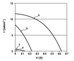
- FIG. 3 illustrates I-V curves of CZTS photovoltaic devices: the curve (a) corresponds to an annealed CZTS layer according to the method of the invention, according to Example 2, the curve (b) corresponds to a CZTS layer annealed in one step under an N 2 atmosphere, according to comparative Example 3; the curve (c) corresponds to a CZTS layer annealed in a step under an H 2 S atmosphere, according to comparative Example 4; the curve (d) corresponds to a CZTS layer annealed in two steps (the first under N 2 , the second under SnS and S vapours), according to comparative Example 8.
- FIG. 4 illustrates the I-V curves of the photovoltaic devices comprising a CZTS layer annealed according to the method of the invention: the curve (a) corresponds to a CZTS layer annealed according to Example 2, the curve (e) corresponds to a CZTS layer annealed according to Example 3, with an additional step for chemical cleaning with hydrochloric acid of the CZTS layer after annealing and before depositing the CdS buffer layer.
- the morphology of the CZTS layers may be checked by scanning electron microscopy (SEM), also optionally by transmission electron microscopy (TEM), in different areas of the layer, in top views or in edge views.
- SEM scanning electron microscopy
- TEM transmission electron microscopy
- the crystalline phases present in the CZTS layers may be analysed by x-ray diffraction (XRD), typically with a grazing angle from 1 to 3 degrees.
- XRD x-ray diffraction
- the average elementary composition of the layers may be analysed by x-ray spectroscopy with energy dispersion (energy dispersive x-ray spectroscopy, EDX or EDS), coupled with an SEM instrument, on surfaces with a size of tens or hundreds of micrometers.
- the homogeneity of the elementary composition may be further evaluated by EDX mapping in top views.
- the photovoltaic performance of the photovoltaic devices is measured from current-voltage (I-V) curves under irradiation of a solar simulator with a standard power of 1,000 W/m 2 . From these curves, the conversion yield of the incident radiation into electric power is calculated at the maximum power point, and other performance parameters such as the photo-current for a short-circuit and the voltage for an open circuit.
- I-V current-voltage
- Example 1 the manufacturing of a thin CZTS layer is described by using a colloidal dispersion of CZTS particles and the double annealing method of the present invention.
- Each annealing step comprises a ramp for raising the temperature from room temperature up to the maximum temperature (typically within a period of 50 minutes), followed by a plateau at this maximum temperature (typically from 15 to 60 minutes), followed by cooling down to room temperature.
- Example 2 the manufacturing of a photovoltaic device made with the thin CZTS layer of Example 1 is described.
- the comparative Examples 3 to 6 layers and devices made with the same technique and then annealed according to an annealing method in a single step (a single atmosphere) are described.
- the CZTS layer of the comparative Example 3, annealed under a neutral nitrogen atmosphere, is compact and has large grains (of the order of one micrometer). It has secondary crystalline phases especially of SnS, as shown by x-ray diffraction analysis (XRD); EDX mapping shows a few areas which are richer in Cu and a few areas which are richer in Zn as compared with the average composition of the layer. Photovoltaic devices made with this type of layer exhibited low yield, of less than 1%.
- the CZTS layer of the comparative Example 4 annealed under an atmosphere containing H 2 S gas diluted in argon or in nitrogen, exhibits very few or no secondary crystalline phases such as SnS, as shown with XRD.
- the layers are not sufficiently dense and the grains are not sufficiently large. Photovoltaic devices made with this type of layer have a very low performance.
- the CZTS layer of the comparative Example 5 annealed under an atmosphere containing elementary S vapour, has very few or no secondary phases such as SnS, as shown with XRD.
- the layers are not sufficiently dense and the grains are not sufficiently large.
- the CZTS layer of the comparative Example 6, annealed under an atmosphere containing SnS vapour, has few secondary phases like SnS, (estimated to be at less than 1%), as shown with XRD.
- the layers are not sufficiently dense and the grains are not sufficiently large.
- the performance of these devices may be improved by more accurate adjustment of the composition of the layer (as known in the state of the art) and by adjustments of the thicknesses and compositions of ancillary layers (buffer layer, front and rear conducting layer).
- the effect of the Mo substrate is shown as compared with a glass substrate during annealing in a neutral atmosphere; the Mo substrate gives the possibility of obtaining a compact layer, unlike the glass substrate.
- Example 11 the manufacturing of a photovoltaic device made with the thin CZTS layer of Example 1 is described, followed by a chemical cleaning step, the photovoltaic device being finished like in Example 2.
- Table 1 hereafter summarizes the results of the analyses of the CZTS layers on a Mo substrate after several types of annealing in one step.
- annealings were carried out in two steps, wherein the first step was annealing under N 2 and the second step was annealing in an atmosphere containing S, SnS+S, or SnS 2 vapours, as described in the comparative Examples 7 to 9, the morphology or the homogeneity of the layers and/or the photovoltaic performance not being satisfactory.
- Table 2 hereafter summarizes the results of the analyses of the CZTS layers on a Mo substrate after several types of annealing in two steps.
- Table 3 hereafter summarizes the performances of the devices made with CZTS layers on Mo annealed with different annealing methods.
- Annealing was carried out with a temperature raising ramp of 50 minutes from room temperature up to the maximum temperature, followed by a plateau at this maximum temperature, followed by cooling down to room temperature either naturally or forced in order to cool faster.
- a colloid of Cu—Zn—Sn—S nanoparticles was made by reacting a mixture of metal salts of CuCl, ZnCl 2 and SnCl 4 .5H 2 O in water/acetonitrile with an aqueous NaSH solution, at room temperature and under a neutral nitrogen atmosphere, according to the global reaction: 2CuCl+ZnCl 2 +SnCl 4 +4NaSH Cu 2 ZnSnS 4 +4NaCl+4HCl
- This reactive system is adapted in the sense that the reaction by-products, for example NaCl or HCl, are soluble in water while the nanoparticles are solid and dispersed as a colloid.
- the reaction by-products for example NaCl or HCl
- a 0.12 M aqueous solution of NaSH in deionized water was prepared.
- a solution of metal chlorides of copper, zinc and tin as mentioned above was prepared in acetonitrile in a glove box with nitrogen, at a concentration of ⁇ 0.5 M of Cu, ⁇ 0.25 M of Zn and ⁇ 0.25 M of Sn (typically 469 mg of CuCl, 415 mg of ZnCl 2 and 893 mg of SnCl 4 .5H 2 O in 10 ml of acetonitrile).
- One volume of the metal chloride solution was taken, and 4 volumes of acetonitrile and 5 volumes of water were added. To this solution, were added 10 volumes of the NaHS solution, rapidly giving a colloidal dispersion.
- the thereby obtained colloid is washed in water and ethanol with successive centrifugation steps, removal of supernatant and re-dispersion.
- the precipitate after the last centrifugation is re-dispersed (and concentrated relatively to the initial volume) by adding 5 volumes of ethanol.
- the particles of the rinsed colloid were analysed by transmission electron microscopy TEM, which showed nanoparticles with a rounded shape, agglomerated and typically with sizes between 2 and 7 nm.
- Deposition of the CZTS film was accomplished by spraying in a glove box filled with nitrogen.
- a colloidal dispersion was prepared by mixing 2 volumes of the final ethanol colloidal dispersion obtained according to paragraph A above with 18 volumes of water.
- Commercial sodium-lime glass substrates with a Mo layer, of dimensions 2.5 ⁇ 2.5 cm, were placed on a heating plate at a temperature of 300° C.
- the nozzle of the spray used was a flask for spraying on a specimen in borosilicate glass.
- nitrogen pressure was controlled intermittently: open for 0.3 seconds and then a waiting period of 1.7 seconds, this 2 second cycle being maintained during the duration for the deposition, which was of 2 minutes and a half.
- the nozzle-substrate distance was about 15 cm with an average flow of nitrogen carrier gas of 14 L/min at a nitrogen cylinder pressure of 0.2 bars above atmospheric pressure. A uniform coloured layer was thus obtained upon examination.
- a first annealing step under an N 2 atmosphere was carried out on a heating plate placed in a glove box filled with dry nitrogen, with a plateau at 525° C. for 15 min (with a rise in temperature designated hereafter by ramp ) for 50 minutes followed by natural cooling down to room temperature around 25-30° C.
- a second annealing step under a H 2 S atmosphere was carried out in a tubular oven, under a flow of 3% H 2 S in argon, with a plateau at 525° C. for 60 minutes with a rise in temperature for 50 minutes and natural cooling down to a room temperature of 20-40° C.
- the layer was dense or compact and the grain size was of the order of 1 ⁇ m, according to an SEM analysis in a top view.
- a view of a section of the film obtained after annealing exhibited thickness of the CZTS film around 2 to 3 ⁇ m.
- the film has a surface roughness with an arithmetic mean height of the peaks, Sa, of 250 nm for analysis surfaces of at least 20 ⁇ 20 ⁇ m 2 .
- the peaks corresponding to the secondary crystalline phase SnS (as shown in FIG. 2 ) were not present or they were very small (for different samples made under the same conditions).
- EDX mapping of the elementary atomic composition of the three metals in the layer revealed a few micrometric areas slightly richer in Zn by more than 10% relatively to the average Cu:Zn:Sn percentage of the layer.
- a buffer layer of CdS of about 50 nm was deposited by chemical deposition (chemical bath deposition, CBD), according to the usual procedure of the state of the art.
- a transparent ZnO layer of about 50 nm was successively deposited, followed by a transparent conductive layer of Sn-doped indium oxide (ITO) of about 250 nm, by magnetron cathode sputtering, by using a commercial apparatus.
- ITO indium oxide
- the substrate was divided into 16 electrically insulated cells, with dimensions of 0.5 ⁇ 0.5 cm.
- a small silver spot was deposited (by drying a silver-loaded paint) onto the transparent front contact layer in order to collect the current and place one of the contacts for measuring the photovoltaic performance.
- the second contact was directly made on the Mo at the edge of the substrate.
- the photovoltaic yield was measured with a standard test by producing current-voltage curves under a solar simulator, as described in patent FR2899385.
- the photovoltaic yield (or photovoltaic efficiency) was calculated from electric current-voltage characteristics of the photovoltaic diode measured under light irradiation.
- This photovoltaic efficiency was measured with an electric test bench and which uses a solar simulator delivering an irradiation of 1,000 W/m 2 corresponding to the AM1.5G standard.
- the measurement bench was calibrated according to the standard procedure on the basis of the known photo-current of reference cells, as provided by various recognized official institutes.
- the best performance was a yield of more than 3%, with open-circuit currents from 10 to 17 mA/cm 2 and open circuit voltages from 0.45 to 0.63 V.
- a layer was prepared like in Example 1, but only annealed with the first step under an N 2 atmosphere. Before annealing, the layer was porous and formed with small grains of the order of ⁇ 10 nm. After this annealing, the layer was dense and the grain size was of the order of 1 ⁇ m. According to XRD analysis, in addition to the CZTS phase, peaks were detected corresponding to the SnS phase. EDX mapping of the elementary atomic composition of the three metals in a few portions of the layer revealed a few micrometric areas very rich in Cu (more than 25%), or richer in Zn, or in Sn relatively to the average Cu:Zn:Sn percentage of the layer.
- photovoltaic devices were manufactured by following the procedure of Example 2.
- the best yield was less than 0.6%
- the short-circuit currents were less than 8 mA/cm 2
- the open circuit voltages were less than 0.25 V.
- the layer after this annealing was not dense, but porous, and the grain size was less than 500 nm. According to XRD analysis, the peaks corresponding to the secondary phase SnS were not present or they were very small (for various samples made under the same conditions).
- photovoltaic devices were manufactured by following the procedure of Example 2. The best yield was ⁇ 0.1%, the short-circuit currents were less than 1 mA/cm 2 and the open circuit voltages were less than 0.1V.
- Example 2 Layers were prepared like in Example 1, but only annealed with a single step, under an atmosphere containing S vapour.
- the annealing was carried out on a heating plate placed in a glove box filled with dry nitrogen: A crucible containing S powder was placed beside the layer to be annealed, both covered by a glass bell, on a heating plate with a lid.
- the heating cycle was similar to that of the annealing under N 2 of Example 3, with a plateau between 550 and 600° C.
- the layer after this annealing was not dense, but porous.
- the grain size was less than 500 nm for the plateau at 550° C., and ⁇ 500 nm-1 ⁇ m or less for the plateaux at 570-600° C. According to XRD analysis, the peaks corresponding the secondary phase SnS were not present or were too small (for various samples made under the same conditions).
- Example 2 Layers were prepared like in Example 1, but only annealed with a single step, under an atmosphere containing SnS vapour.
- the annealing was carried out on a heating plate placed in a glove box filled with dry nitrogen: A crucible containing SnS powder was placed beside the layer to be annealed, both covered by a glass bell, on a heating plate with a lid.
- the heating cycle is similar to that of the annealing under N 2 of Example 3, with a plateau between 525 and 550° C.
- the layer after the annealing with the plateau at 525° C. was not dense but porous and the grain size was less than 500 nm.
- the layer after the annealing with the plateau at 550° C. was dense and the grain size was of the order of 1 ⁇ m.
- the peaks corresponding to the secondary phase SnS were present for the layer after the annealing with the plateau at 525° C., and they were more intense for the layer after the annealing with the plateau at 550° C.
- a layer was prepared like in Example 1, annealed with two steps, a first step under an N 2 atmosphere (like in Example 1), and a second step in an atmosphere containing S vapour (and not H 2 S like in Example 1).
- the second annealing step was carried out on a heating plate placed in a glove box filled with dry nitrogen: A crucible containing S was placed beside the layer to be annealed, both covered by a glass bell, on a heating plate with a lid.
- the heating cycle was similar to that of the annealing under N 2 of Example 3, with a plateau at 525° C.
- the layer after this annealing was dense, but the grains exhibited at the surface a corroded aspect different from that of Example 1, as if it had been etched. According to XRD analysis, the peaks corresponding to the secondary phase SnS were present.
- a thin CZTS layer by using a colloidal dispersion of CZTS and annealed with an annealing method in two steps, a first annealing step in a neutral atmosphere, and a second step in an atmosphere containing SnS and S vapours, and of a photovoltaic device of the thin layer type made with this layer.
- a layer was prepared like in Example 1, annealed with two steps, a first step under an N 2 atmosphere (like in Example 1), and a second step in an atmosphere containing SnS and S vapours (and not H 2 S like in Example 1).
- the second annealing step was carried out on a heating plate placed in a glove box filled with dry nitrogen: A crucible containing SnS and S powder was placed beside the layer to be annealed, both covered by a glass bell, on a heating plate with a lid.
- the heating cycle was similar to that of the annealing under N 2 of Example 3, with a plateau at 525° C.
- the layer after this annealing was dense, with the presence of an overlayer with an aspect different from that of Example 1, without well-defined grain boundaries. According to XRD analyses, the peaks corresponding to the secondary phase SnS were very small.
- a thin CZTS layer by using a colloidal dispersion of CZTS and annealed with an annealing method in two steps, a first one in a neutral atmosphere, and a second one in an atmosphere containing SnS 2 vapour, and of a photovoltaic device of the thin layer type made with this layer.
- a layer was prepared like in Example 1, annealed with two steps, a first step under a N 2 atmosphere (like in Example 1), and a second step in an atmosphere containing SnS 2 vapour (and not H 2 S like in Example 1).
- the second annealing step was carried out on a heating plate placed in a glove box filled with dry nitrogen: A crucible containing SnS 2 powder was placed beside the layer to be annealed, both covered by a glass bell on a heating plate with a lid.
- the heating cycle was similar to that of the annealing under N 2 of Example 3, with a plateau at 525° C.
- the layer after this annealing was dense. According to XRD analyses, the peaks corresponding to the secondary phase SnS were very small.
- a layer was prepared like in Example 3, but on a sodium-lime glass substrate without any molybdenum layer, and only annealed with the first step under an N 2 atmosphere.
- the layer was not dense, but porous, and the average grain size was less than 500 nm.
- Example 2 The CZTS layer of Example 1 was immersed in a solution of 8% by weight hydrochloric acid, HCl, for 1 to 2 minutes. It was then rinsed with deionized water and dried under a nitrogen flow. Immediately after this, the buffer layer CdS and the remainder of the layers were deposited for finishing the photovoltaic device like in Example 2.
- the layer shown in this example had a thickness and roughness identical with that of Example 2.
- Vco and the form factor for the obtained photovoltaic device according to this example are in the same range of values as for the photovoltaic devices of Example 2.
Landscapes
- Engineering & Computer Science (AREA)
- Chemical & Material Sciences (AREA)
- Physics & Mathematics (AREA)
- Condensed Matter Physics & Semiconductors (AREA)
- General Physics & Mathematics (AREA)
- Computer Hardware Design (AREA)
- Microelectronics & Electronic Packaging (AREA)
- Power Engineering (AREA)
- Manufacturing & Machinery (AREA)
- Electromagnetism (AREA)
- Inorganic Chemistry (AREA)
- Crystallography & Structural Chemistry (AREA)
- Chemical Kinetics & Catalysis (AREA)
- Materials Engineering (AREA)
- Mechanical Engineering (AREA)
- Metallurgy (AREA)
- Organic Chemistry (AREA)
- Sustainable Energy (AREA)
- Sustainable Development (AREA)
- Life Sciences & Earth Sciences (AREA)
- Nanotechnology (AREA)
- General Chemical & Material Sciences (AREA)
- Thermal Sciences (AREA)
- Ceramic Engineering (AREA)
- Photovoltaic Devices (AREA)
Applications Claiming Priority (3)
| Application Number | Priority Date | Filing Date | Title |
|---|---|---|---|
| FR1350741 | 2013-01-29 | ||
| FR1350741A FR3001467B1 (fr) | 2013-01-29 | 2013-01-29 | Procede de preparation de couche mince d'absorbeur a base de sulfure(s) de cuivre, zinc et etain, couche mince recuite et dispositif photovoltaique obtenu |
| PCT/FR2013/052851 WO2014118444A1 (fr) | 2013-01-29 | 2013-11-26 | Procédé de préparation de couche mince d'absorbeur à base de sulfure(s) de cuivre, zinc et étain, couche mince recuite et dispositif photovoltaïque obtenu |
Publications (2)
| Publication Number | Publication Date |
|---|---|
| US20150333212A1 US20150333212A1 (en) | 2015-11-19 |
| US9391231B2 true US9391231B2 (en) | 2016-07-12 |
Family
ID=48570235
Family Applications (1)
| Application Number | Title | Priority Date | Filing Date |
|---|---|---|---|
| US14/758,314 Active US9391231B2 (en) | 2013-01-29 | 2013-11-26 | Method for preparing a thin layer of an absorber made of copper, zinc and tin sulfide(s), annealed thin layer and photovoltaic device thus obtained |
Country Status (5)
| Country | Link |
|---|---|
| US (1) | US9391231B2 (ja) |
| EP (1) | EP2951855B1 (ja) |
| JP (1) | JP2016510506A (ja) |
| FR (1) | FR3001467B1 (ja) |
| WO (1) | WO2014118444A1 (ja) |
Families Citing this family (9)
| Publication number | Priority date | Publication date | Assignee | Title |
|---|---|---|---|---|
| FR2993792B1 (fr) * | 2012-07-26 | 2017-09-15 | Imra Europe Sas | Film de chalcogenure(s) metallique(s) cristallise(s) a gros grains, solution colloidale de particules amorphes et procedes de preparation. |
| WO2017106160A1 (en) * | 2015-12-15 | 2017-06-22 | Board Of Regents, The University Of Texas System | Nanostructured conducting films with a heterogeneous dopant distribution and methods of making and use thereof |
| KR101983320B1 (ko) * | 2017-04-05 | 2019-05-29 | 전남대학교산학협력단 | 기상 증착법을 이용한 황화주석 박막 및 이의 형성방법 |
| CN109956495B (zh) * | 2017-12-25 | 2020-12-22 | 中国科学院物理研究所 | 直立交错式花瓣状二硫化锡纳米片及其制备方法 |
| AT521545A1 (de) * | 2018-08-09 | 2020-02-15 | Ait Austrian Inst Tech Gmbh | Suspension zur herstellung einer halbleiterschicht |
| CN111822013B (zh) * | 2020-07-06 | 2022-11-18 | 重庆大学 | 一种单胞pn结及其精准构筑方法 |
| KR102408206B1 (ko) * | 2021-10-28 | 2022-06-15 | 전남대학교산학협력단 | 표면 결함이 제어된 SnS계 박막 태양전지 및 이의 제조방법 |
| CN114899280A (zh) * | 2022-05-11 | 2022-08-12 | 中南大学 | 一种镉掺杂的铜锌锡硫硒薄膜制备方法及其在太阳能电池中的应用 |
| CN114988715B (zh) * | 2022-05-25 | 2023-06-27 | 中南大学 | 一种铜锌锡硫薄膜的制备方法 |
Citations (6)
| Publication number | Priority date | Publication date | Assignee | Title |
|---|---|---|---|---|
| US20110094557A1 (en) * | 2009-10-27 | 2011-04-28 | International Business Machines Corporation | Method of forming semiconductor film and photovoltaic device including the film |
| WO2012071287A1 (en) | 2010-11-22 | 2012-05-31 | E. I. Du Pont De Nemours And Company | Inks and processes to make a chalcogen-containing semiconductor |
| WO2012071289A2 (en) | 2010-11-22 | 2012-05-31 | E. I. Du Pont De Nemours And Company | Semiconductor inks, films and processes for preparing coated substrates and photovoltaic devices |
| WO2012071288A1 (en) | 2010-11-22 | 2012-05-31 | E. I. Du Pont De Nemours And Company | Semiconductor inks, films, coated substrates and methods of preparation |
| US20120220066A1 (en) * | 2009-11-25 | 2012-08-30 | E.I. Du Pont De Nemours And Company | Czts/se precursor inks and methods for preparing czts/se thin films and czts/se-based photovoltaic cells |
| US20140182665A1 (en) * | 2012-12-27 | 2014-07-03 | Intermolecular, Inc. | Optical Absorbers |
Family Cites Families (1)
| Publication number | Priority date | Publication date | Assignee | Title |
|---|---|---|---|---|
| FR2899385B1 (fr) | 2006-03-31 | 2008-06-27 | Imra Europ Sas Soc Par Actions | Dispositif photovoltaique tout solide comprenant une couche d'absorbeur a base de sulfure d'antimoine |
-
2013
- 2013-01-29 FR FR1350741A patent/FR3001467B1/fr not_active Expired - Fee Related
- 2013-11-26 US US14/758,314 patent/US9391231B2/en active Active
- 2013-11-26 JP JP2015554225A patent/JP2016510506A/ja active Pending
- 2013-11-26 WO PCT/FR2013/052851 patent/WO2014118444A1/fr active Application Filing
- 2013-11-26 EP EP13803174.5A patent/EP2951855B1/fr active Active
Patent Citations (7)
| Publication number | Priority date | Publication date | Assignee | Title |
|---|---|---|---|---|
| US20110094557A1 (en) * | 2009-10-27 | 2011-04-28 | International Business Machines Corporation | Method of forming semiconductor film and photovoltaic device including the film |
| US20120220066A1 (en) * | 2009-11-25 | 2012-08-30 | E.I. Du Pont De Nemours And Company | Czts/se precursor inks and methods for preparing czts/se thin films and czts/se-based photovoltaic cells |
| WO2012071287A1 (en) | 2010-11-22 | 2012-05-31 | E. I. Du Pont De Nemours And Company | Inks and processes to make a chalcogen-containing semiconductor |
| WO2012071289A2 (en) | 2010-11-22 | 2012-05-31 | E. I. Du Pont De Nemours And Company | Semiconductor inks, films and processes for preparing coated substrates and photovoltaic devices |
| WO2012071288A1 (en) | 2010-11-22 | 2012-05-31 | E. I. Du Pont De Nemours And Company | Semiconductor inks, films, coated substrates and methods of preparation |
| US20140048137A1 (en) * | 2010-11-22 | 2014-02-20 | E I Du Pont De Nemours And Company | Process for preparing coated substrates and photovoltaic devices |
| US20140182665A1 (en) * | 2012-12-27 | 2014-07-03 | Intermolecular, Inc. | Optical Absorbers |
Non-Patent Citations (4)
| Title |
|---|
| Ankur Khare: "Synthesis and Characterization of Copper Zinc Tin Sulfide Nanoparticles and Thin Films", Jun. 30, 2012, Retrieved from the Internet: URL:http://conservancy.umn.edu/bitstream/133748/1/Khare-umn-0130E-12926.pdf. |
| International Search Report mailed Feb. 3, 2014, corresponding to International Patent Application PCT/FR2013/052851. |
| Kazuya Maeda et al: "Influence of H2S concentration on the properties of Cu2ZnSnS4 thin films and solar cells prepared by sol gel sulfurization", Solar Energy Materials and Solar Cells, Elsevier Science Publishers, Amsterdam, NL, vol. 95, No. 10, May 31, 2011, pp. 2855-2860. |
| Tanaka et al.: "Preparation of Cu2ZnSnS4 thin films by sulfurizing sol-gel deposited precursors", Solar Energy Materials and Solar Cells, Elsevier Science Publishers, Amsterdam, NL, vol. 91, No. 13, Jun. 5, 2007, pp. 1199-1201. |
Also Published As
| Publication number | Publication date |
|---|---|
| EP2951855A1 (fr) | 2015-12-09 |
| JP2016510506A (ja) | 2016-04-07 |
| US20150333212A1 (en) | 2015-11-19 |
| EP2951855B1 (fr) | 2018-10-24 |
| FR3001467A1 (fr) | 2014-08-01 |
| WO2014118444A1 (fr) | 2014-08-07 |
| FR3001467B1 (fr) | 2016-05-13 |
Similar Documents
| Publication | Publication Date | Title |
|---|---|---|
| US9391231B2 (en) | Method for preparing a thin layer of an absorber made of copper, zinc and tin sulfide(s), annealed thin layer and photovoltaic device thus obtained | |
| JP4303363B2 (ja) | 酸化物に基づき、化合物半導体膜を製造し、更に関連する電子デバイスを製造する方法 | |
| US20200215509A1 (en) | Method of manufacturing a large-grain crystallized metal chalcogenide film, and a crystallized metal chalcogenide film prepared using the method | |
| US20120279565A1 (en) | Method of forming semiconductor film and photovoltaic device including the film | |
| WO2012023519A1 (ja) | 化合物半導体薄膜作製用インク、そのインクを用いて得た化合物半導体薄膜、その化合物半導体薄膜を備える太陽電池、およびその太陽電池の製造方法 | |
| TW200834944A (en) | Doping techniques for group IB III AVIA compound layers | |
| JP6688832B2 (ja) | アンチモンがドープされたナノ粒子 | |
| KR101149474B1 (ko) | 용액상 볼밀법을 이용한 cis계 또는 czts계 콜로이드 용액 및 이를 이용한 태양전지 광흡수층 cis계 또는 czts계 화합물 박막의 제조방법 | |
| JP5967837B2 (ja) | 化合物半導体薄膜形成用インクの製造方法 | |
| Farhana et al. | Recent advances and new research trends in Sb2S3 thin film based solar cells | |
| TWI552373B (zh) | 具有高無裂縫限度之cigs奈米粒子墨水調配物 | |
| WO2012090938A1 (ja) | 化合物半導体薄膜太陽電池及びその製造方法 | |
| WO2015185834A1 (fr) | Procédé de préparation de couche mince d'absorbeur a base de sulfure(s) et séléniures(s) de cuivre, zinc et étain, couche mince recuite et dispositif photovoltaïque obtenus | |
| Wang et al. | Progress and prospectives of solution-processed kesterite absorbers for photovoltaic applications | |
| KR101815277B1 (ko) | 구리가 풍부한 구리 인듐 (갈륨) 디셀레나이드/디설파이드 나노 입자의 제조 | |
| KR101463327B1 (ko) | 스프레이법을 이용한 화합물 태양전지용 CuInSe₂박막의 제조방법 | |
| Ananthoju | Cu₂ZnSnS₄ nanoparticulate thin films and their solar cell characteristics | |
| JP2014086527A (ja) | 化合物半導体薄膜、その製造方法および太陽電池 | |
| JP2014167998A (ja) | 化合物半導体薄膜、その製造方法、および太陽電池モジュール |
Legal Events
| Date | Code | Title | Description |
|---|---|---|---|
| AS | Assignment |
Owner name: IMRA EUROPE SAS, FRANCE Free format text: ASSIGNMENT OF ASSIGNORS INTEREST;ASSIGNORS:JACOB, ALAIN;LARRAMONA, GERARDO;BOURDAIS, STEPHANE;AND OTHERS;SIGNING DATES FROM 20150611 TO 20150619;REEL/FRAME:035938/0239 |
|
| STCF | Information on status: patent grant |
Free format text: PATENTED CASE |
|
| MAFP | Maintenance fee payment |
Free format text: PAYMENT OF MAINTENANCE FEE, 4TH YEAR, LARGE ENTITY (ORIGINAL EVENT CODE: M1551); ENTITY STATUS OF PATENT OWNER: LARGE ENTITY Year of fee payment: 4 |
|
| FEPP | Fee payment procedure |
Free format text: MAINTENANCE FEE REMINDER MAILED (ORIGINAL EVENT CODE: REM.); ENTITY STATUS OF PATENT OWNER: LARGE ENTITY |