US9136392B2 - Semiconductor memory device and method for manufacturing the same - Google Patents
Semiconductor memory device and method for manufacturing the same Download PDFInfo
- Publication number
- US9136392B2 US9136392B2 US13/971,220 US201313971220A US9136392B2 US 9136392 B2 US9136392 B2 US 9136392B2 US 201313971220 A US201313971220 A US 201313971220A US 9136392 B2 US9136392 B2 US 9136392B2
- Authority
- US
- United States
- Prior art keywords
- film
- conductor
- trench
- memory
- hole
- Prior art date
- Legal status (The legal status is an assumption and is not a legal conclusion. Google has not performed a legal analysis and makes no representation as to the accuracy of the status listed.)
- Expired - Fee Related, expires
Links
- 239000004065 semiconductor Substances 0.000 title claims description 18
- 238000000034 method Methods 0.000 title description 14
- 238000004519 manufacturing process Methods 0.000 title description 5
- 239000004020 conductor Substances 0.000 claims abstract description 68
- 230000002093 peripheral effect Effects 0.000 claims abstract description 44
- 238000003860 storage Methods 0.000 claims abstract description 15
- XUIMIQQOPSSXEZ-UHFFFAOYSA-N Silicon Chemical compound [Si] XUIMIQQOPSSXEZ-UHFFFAOYSA-N 0.000 claims description 38
- 229910052710 silicon Inorganic materials 0.000 claims description 38
- 239000010703 silicon Substances 0.000 claims description 38
- 239000012535 impurity Substances 0.000 claims description 17
- 229910052751 metal Inorganic materials 0.000 claims description 6
- 239000002184 metal Substances 0.000 claims description 6
- WFKWXMTUELFFGS-UHFFFAOYSA-N tungsten Chemical group [W] WFKWXMTUELFFGS-UHFFFAOYSA-N 0.000 claims description 3
- 229910052721 tungsten Inorganic materials 0.000 claims description 3
- 239000010937 tungsten Substances 0.000 claims description 3
- 239000010410 layer Substances 0.000 description 70
- ZOXJGFHDIHLPTG-UHFFFAOYSA-N Boron Chemical compound [B] ZOXJGFHDIHLPTG-UHFFFAOYSA-N 0.000 description 10
- 229910052796 boron Inorganic materials 0.000 description 10
- 229910021420 polycrystalline silicon Inorganic materials 0.000 description 10
- 229920005591 polysilicon Polymers 0.000 description 10
- 238000005530 etching Methods 0.000 description 8
- 230000006870 function Effects 0.000 description 8
- 230000008569 process Effects 0.000 description 7
- 239000000758 substrate Substances 0.000 description 7
- KWYUFKZDYYNOTN-UHFFFAOYSA-M Potassium hydroxide Chemical compound [OH-].[K+] KWYUFKZDYYNOTN-UHFFFAOYSA-M 0.000 description 6
- VYPSYNLAJGMNEJ-UHFFFAOYSA-N Silicium dioxide Chemical compound O=[Si]=O VYPSYNLAJGMNEJ-UHFFFAOYSA-N 0.000 description 5
- 230000000052 comparative effect Effects 0.000 description 5
- 239000000463 material Substances 0.000 description 5
- 229910052814 silicon oxide Inorganic materials 0.000 description 5
- OAICVXFJPJFONN-UHFFFAOYSA-N Phosphorus Chemical compound [P] OAICVXFJPJFONN-UHFFFAOYSA-N 0.000 description 4
- 239000011574 phosphorus Substances 0.000 description 4
- 229910052698 phosphorus Inorganic materials 0.000 description 4
- 238000001039 wet etching Methods 0.000 description 4
- 229910052581 Si3N4 Inorganic materials 0.000 description 3
- 230000015572 biosynthetic process Effects 0.000 description 3
- 239000007788 liquid Substances 0.000 description 3
- 238000001020 plasma etching Methods 0.000 description 3
- HQVNEWCFYHHQES-UHFFFAOYSA-N silicon nitride Chemical compound N12[Si]34N5[Si]62N3[Si]51N64 HQVNEWCFYHHQES-UHFFFAOYSA-N 0.000 description 3
- 239000000126 substance Substances 0.000 description 3
- PXHVJJICTQNCMI-UHFFFAOYSA-N Nickel Chemical compound [Ni] PXHVJJICTQNCMI-UHFFFAOYSA-N 0.000 description 2
- 238000005229 chemical vapour deposition Methods 0.000 description 2
- 238000005304 joining Methods 0.000 description 2
- 230000008901 benefit Effects 0.000 description 1
- 230000015556 catabolic process Effects 0.000 description 1
- 229910017052 cobalt Inorganic materials 0.000 description 1
- 239000010941 cobalt Substances 0.000 description 1
- GUTLYIVDDKVIGB-UHFFFAOYSA-N cobalt atom Chemical compound [Co] GUTLYIVDDKVIGB-UHFFFAOYSA-N 0.000 description 1
- 230000007423 decrease Effects 0.000 description 1
- 239000012212 insulator Substances 0.000 description 1
- 230000004048 modification Effects 0.000 description 1
- 238000012986 modification Methods 0.000 description 1
- 229910052759 nickel Inorganic materials 0.000 description 1
- 238000000206 photolithography Methods 0.000 description 1
- 238000005036 potential barrier Methods 0.000 description 1
- 230000009467 reduction Effects 0.000 description 1
- 229910021332 silicide Inorganic materials 0.000 description 1
- FVBUAEGBCNSCDD-UHFFFAOYSA-N silicide(4-) Chemical compound [Si-4] FVBUAEGBCNSCDD-UHFFFAOYSA-N 0.000 description 1
- 239000002356 single layer Substances 0.000 description 1
- 238000005549 size reduction Methods 0.000 description 1
- 238000006467 substitution reaction Methods 0.000 description 1
Images


Classifications
-
- H—ELECTRICITY
- H01—ELECTRIC ELEMENTS
- H01L—SEMICONDUCTOR DEVICES NOT COVERED BY CLASS H10
- H01L29/00—Semiconductor devices specially adapted for rectifying, amplifying, oscillating or switching and having potential barriers; Capacitors or resistors having potential barriers, e.g. a PN-junction depletion layer or carrier concentration layer; Details of semiconductor bodies or of electrodes thereof ; Multistep manufacturing processes therefor
- H01L29/66—Types of semiconductor device ; Multistep manufacturing processes therefor
- H01L29/68—Types of semiconductor device ; Multistep manufacturing processes therefor controllable by only the electric current supplied, or only the electric potential applied, to an electrode which does not carry the current to be rectified, amplified or switched
- H01L29/76—Unipolar devices, e.g. field effect transistors
- H01L29/772—Field effect transistors
- H01L29/78—Field effect transistors with field effect produced by an insulated gate
- H01L29/788—Field effect transistors with field effect produced by an insulated gate with floating gate
-
- H01L27/11521—
-
- H01L27/11551—
-
- H01L27/11556—
-
- H01L27/11582—
-
- H—ELECTRICITY
- H01—ELECTRIC ELEMENTS
- H01L—SEMICONDUCTOR DEVICES NOT COVERED BY CLASS H10
- H01L29/00—Semiconductor devices specially adapted for rectifying, amplifying, oscillating or switching and having potential barriers; Capacitors or resistors having potential barriers, e.g. a PN-junction depletion layer or carrier concentration layer; Details of semiconductor bodies or of electrodes thereof ; Multistep manufacturing processes therefor
- H01L29/66—Types of semiconductor device ; Multistep manufacturing processes therefor
- H01L29/66007—Multistep manufacturing processes
- H01L29/66075—Multistep manufacturing processes of devices having semiconductor bodies comprising group 14 or group 13/15 materials
- H01L29/66227—Multistep manufacturing processes of devices having semiconductor bodies comprising group 14 or group 13/15 materials the devices being controllable only by the electric current supplied or the electric potential applied, to an electrode which does not carry the current to be rectified, amplified or switched, e.g. three-terminal devices
- H01L29/66409—Unipolar field-effect transistors
- H01L29/66477—Unipolar field-effect transistors with an insulated gate, i.e. MISFET
- H01L29/66825—Unipolar field-effect transistors with an insulated gate, i.e. MISFET with a floating gate
-
- H—ELECTRICITY
- H01—ELECTRIC ELEMENTS
- H01L—SEMICONDUCTOR DEVICES NOT COVERED BY CLASS H10
- H01L29/00—Semiconductor devices specially adapted for rectifying, amplifying, oscillating or switching and having potential barriers; Capacitors or resistors having potential barriers, e.g. a PN-junction depletion layer or carrier concentration layer; Details of semiconductor bodies or of electrodes thereof ; Multistep manufacturing processes therefor
- H01L29/66—Types of semiconductor device ; Multistep manufacturing processes therefor
- H01L29/66007—Multistep manufacturing processes
- H01L29/66075—Multistep manufacturing processes of devices having semiconductor bodies comprising group 14 or group 13/15 materials
- H01L29/66227—Multistep manufacturing processes of devices having semiconductor bodies comprising group 14 or group 13/15 materials the devices being controllable only by the electric current supplied or the electric potential applied, to an electrode which does not carry the current to be rectified, amplified or switched, e.g. three-terminal devices
- H01L29/66409—Unipolar field-effect transistors
- H01L29/66477—Unipolar field-effect transistors with an insulated gate, i.e. MISFET
- H01L29/66833—Unipolar field-effect transistors with an insulated gate, i.e. MISFET with a charge trapping gate insulator, e.g. MNOS transistors
-
- H—ELECTRICITY
- H01—ELECTRIC ELEMENTS
- H01L—SEMICONDUCTOR DEVICES NOT COVERED BY CLASS H10
- H01L29/00—Semiconductor devices specially adapted for rectifying, amplifying, oscillating or switching and having potential barriers; Capacitors or resistors having potential barriers, e.g. a PN-junction depletion layer or carrier concentration layer; Details of semiconductor bodies or of electrodes thereof ; Multistep manufacturing processes therefor
- H01L29/66—Types of semiconductor device ; Multistep manufacturing processes therefor
- H01L29/68—Types of semiconductor device ; Multistep manufacturing processes therefor controllable by only the electric current supplied, or only the electric potential applied, to an electrode which does not carry the current to be rectified, amplified or switched
- H01L29/76—Unipolar devices, e.g. field effect transistors
- H01L29/772—Field effect transistors
- H01L29/78—Field effect transistors with field effect produced by an insulated gate
- H01L29/792—Field effect transistors with field effect produced by an insulated gate with charge trapping gate insulator, e.g. MNOS-memory transistors
- H01L29/7926—Vertical transistors, i.e. transistors having source and drain not in the same horizontal plane
-
- H—ELECTRICITY
- H10—SEMICONDUCTOR DEVICES; ELECTRIC SOLID-STATE DEVICES NOT OTHERWISE PROVIDED FOR
- H10B—ELECTRONIC MEMORY DEVICES
- H10B41/00—Electrically erasable-and-programmable ROM [EEPROM] devices comprising floating gates
- H10B41/20—Electrically erasable-and-programmable ROM [EEPROM] devices comprising floating gates characterised by three-dimensional arrangements, e.g. with cells on different height levels
- H10B41/23—Electrically erasable-and-programmable ROM [EEPROM] devices comprising floating gates characterised by three-dimensional arrangements, e.g. with cells on different height levels with source and drain on different levels, e.g. with sloping channels
- H10B41/27—Electrically erasable-and-programmable ROM [EEPROM] devices comprising floating gates characterised by three-dimensional arrangements, e.g. with cells on different height levels with source and drain on different levels, e.g. with sloping channels the channels comprising vertical portions, e.g. U-shaped channels
-
- H—ELECTRICITY
- H10—SEMICONDUCTOR DEVICES; ELECTRIC SOLID-STATE DEVICES NOT OTHERWISE PROVIDED FOR
- H10B—ELECTRONIC MEMORY DEVICES
- H10B41/00—Electrically erasable-and-programmable ROM [EEPROM] devices comprising floating gates
- H10B41/30—Electrically erasable-and-programmable ROM [EEPROM] devices comprising floating gates characterised by the memory core region
-
- H—ELECTRICITY
- H10—SEMICONDUCTOR DEVICES; ELECTRIC SOLID-STATE DEVICES NOT OTHERWISE PROVIDED FOR
- H10B—ELECTRONIC MEMORY DEVICES
- H10B43/00—EEPROM devices comprising charge-trapping gate insulators
- H10B43/20—EEPROM devices comprising charge-trapping gate insulators characterised by three-dimensional arrangements, e.g. with cells on different height levels
- H10B43/23—EEPROM devices comprising charge-trapping gate insulators characterised by three-dimensional arrangements, e.g. with cells on different height levels with source and drain on different levels, e.g. with sloping channels
- H10B43/27—EEPROM devices comprising charge-trapping gate insulators characterised by three-dimensional arrangements, e.g. with cells on different height levels with source and drain on different levels, e.g. with sloping channels the channels comprising vertical portions, e.g. U-shaped channels
Definitions
- Embodiments described herein relate generally to a semiconductor memory device and a method for manufacturing the same.
- a structure is known in which, in a chip including a memory cell transistor of a stack gate structure in which a floating gate and a control gate are stacked, a resistance element of a peripheral circuit is formed using polysilicon of the floating gate.
- a memory device of a three-dimensional structure in which a memory hole is formed in a stacked body in which an electrode film functioning as the control gate of a memory cell and an inter-electrode insulating film are alternately stacked in plural, and a silicon body serving as a channel is provided on the side wall of the memory hole via a charge storage film.
- the resistance element it is required also for the resistance element to have a different structure from a memory device of a two-dimensional structure.
- FIG. 1 is a schematic cross-sectional view of a semiconductor memory device of a first embodiment
- FIG. 2 is a schematic perspective view of a memory array cell in the semiconductor memory device of the embodiment:
- FIG. 3 is a schematic cross-sectional view of a part of the memory cell array in FIG. 2 ;
- FIG. 4 is a schematic plan view of a resistance element in the semiconductor memory device of the embodiment:
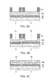
- FIG. 5A to FIG. 13 are schematic cross-sectional views showing a method for manufacturing the semiconductor memory device of the first embodiment
- FIG. 14 is a schmatic cross-sectional view of a semiconductor memory device of a second embodiment
- FIG. 15 is a schematic cross-sectional view showing a method for manufacturing the semiconductor memory device of the second embodiment
- FIG. 16 is a schematic cross-sectional view of a variation of the semiconductor memory device of the second embodiment.
- FIG. 17A is a schematic plan view showing a planar shape of a resistance element of a comparative example.
- FIG. 17B is a schematic plan view showing a planar shape of the resistance element of the embodiment.
- a semiconductor memory device includes an underlying film, a stacked body, a channel body, a memory film and a conductor.
- the underlying film includes a memory region and a peripheral region.
- the memory region includes a first trench
- the peripheral region includes a second trench.
- the stacked body includes a plurality of conductive layers and a plurality of insulating layers alternately stacked on the underlying film.
- the channel body is provided in a pair of first holes and in the first trench.
- the pair of first holes pierces the stacked body on the memory region to be connected to the first trench.
- the memory film includes a charge storage film provided between a side wall of the first hole and the channel body, and between an inner wall of the first trench and the channel body.
- the conductor is provided in a pair of second holes and in the second trench. The pair of second holes pierces the stacked body on the peripheral region to be connected to the second trench and has a hole diameter larger than a hole diameter of the first hole.
- FIG. 1 is a schematic cross-sectional view of a semiconductor memory device of a first embodiment.
- the semiconductor memory device of the embodiment includes a stacked body in which a conductive layer WL and an insulating layer 42 are alternately stacked in plural.
- the stacked body is provided on a back gate BG as an underlying film.
- the back gate BG is a conductive film, and is, for example, a silicon film doped with an impurity.
- the back gate BG is provided on a substrate 10 shown in FIGS. 5A to 5C via an insulating layer 40 .
- the back gate BG is roughly divided into a memory region 2 and a peripheral region 3 around the memory region 2 .
- a memory cell array 4 is provided in the memory region 2 .
- FIG. 2 is a schematic perspective view of the memory cell array 4 .
- the illustration of the insulating portions is omitted for easier viewing of the drawing.
- an XYZ orthogonal coordinate system is introduced.
- Two directions parallel to the major surface of the substrate 10 and orthogonal to each other are defined as the X direction (a first direction) and the Y direction (a second direction), and the direction orthogonal to both of the X direction and the Y direction is defined as the Z direction (the stacking direction of the stacked body or a third direction).
- the cross section of the memory cell array 4 shown in FIG. 1 shows a cross section parallel to the XZ plane in FIG. 2 .
- the memory cell array 4 includes a plurality of memory strings MS.
- One memory string MS is formed in a U-shaped configuration including a pair of columnar portions CL extending in the Z direction and a joining portion JP joining the lower ends of the pair of columnar portions CL.
- FIG. 3 shows an enlarged cross-sectional view of the columnar portion CL of the memory string MS.
- An insulating layer 41 is provided on the back gate BG as shown in FIG. 1 .
- the conductive layer WL and the insulating layer 42 are alternately stacked in plural on the insulating layer 41 .
- the number of conductive layers WL shown in FIG. 1 is an example, and the number of conductive layers WL is arbitrary.
- the conductive layer WL is a polysilicon film doped with, for example, boron as an impurity (a first silicon film), and has an electrical conductivity sufficient to function as the gate electrode of a memory cell.
- the insulating layers 41 and 42 are, for example, a film mainly containing silicon oxide. Alternatively, a film mainly containing silicon nitride may be used as the insulating layers 41 and 42 .
- a drain-side select gate SGD is provided in the upper end portion of one of the pair of columnar portions CL of the U-shaped memory string MS, and a source-side select gate SGS is provided in the upper end portion of the other of the pair of columnar portions CL.
- the drain-side select gate SGD and the source-side select gate SGS are provided on the uppermost conductive layer WL via an insulating layer 43 .
- the drain-side select gate SGD and the source-side select gate SGS are a polysilicon film doped with, for example, boron as an impurity, and have an electrical conductivity sufficient to function as the gate electrode of a select transistor.
- the thickness of the drain-side select gate SGD and the thickness of the source-side select gate SGS are thicker than the thickness of each of the conductive layers WL.
- the drain-side select gate SGD and the source-side select gate SGS are divided in the X direction by an insulating film 74 shown in FIG. 1 .
- the conductive layer WL stacked under the drain-side select gate SGD and the conductive layer WL stacked under the source-side select gate SGS are divided in the X direction by an insulating film 72 .
- Also the stacked body between memory strings MS adjacent in the X direction is divided in the X direction by the insulating film 72 .
- a source line SL shown in FIG. 2 is provided on the source-side select gate SGS via an insulating layer 44 shown in FIG. 1 .
- the source line SL is, for example, a metal film.
- Bit lines BL that are a plurality of metal interconnections are provided on the drain-side select gate SGD and the source line SL via the insulating layer 44 . Each bit line BL extends in the X direction.
- the memory string MS includes a channel body 20 provided in a U-shaped memory hole MH (shown in FIG. 9 ) formed in the stacked body including the back gate BG, the plurality of conductive layers WL, the insulating layers 41 to 44 , the drain-side select gate SGD, and the source-side select gate SGS.
- the channel body 20 is provided in the U-shaped memory hole MH via a memory film 30 .
- the memory film 30 is provided between the side wall of the memory hole MH (a first hole 53 ) and the channel body 20 .
- the channel body 20 is, for example, a non-doped silicon film.
- “non-doped” means that an impurity for providing electrical conductivity is not intentionally added to the silicon film and impurities are not substantially contained other than the elements resulting from the source gas in the film-formation.
- FIG. 3 illustrates a structure in which the channel body 20 is provided such that a hollow portion remains on the central axis side of the memory hole MH (the first hole 53 ), the entire space in the memory hole MH (the first hole 53 ) may be filled up with the channel body 20 , or a structure in which an insulator is buried in the hollow portion on the inside of the channel body 20 is possible.
- the memory film 30 includes a block film 31 , a charge storage film 32 , and a tunnel film 33 .
- the block film 31 , the charge storage film 32 , and the tunnel film 33 are provided in this order from the conductive layer WL side between each conductive layer WL and the channel body 20 .
- the block film 31 is in contact with each conductive layer WL
- the tunnel film 33 is in contact with the channel body 20
- the charge storage film 32 is provided between the block film 31 and the tunnel film 33 .
- the channel body 20 functions as a channel in a memory cell
- the conductive layer WL functions as the control gate of the memory cell
- the charge storage film 32 functions as a data memory layer that stores a charge injected from the channel body 20 . That is, a memory cell with a structure in which the control gate surrounds the periphery of the channel is formed at the intersection between the channel body 20 and each conductive layer WL.
- the semiconductor memory device of the embodiment is a nonvolatile semiconductor memory device that can perform the erasing and writing of data electrically in a free manner and can retain the memory content even when the power is turned off.
- the memory cell is, for example, a charge trap memory cell.
- the charge storage film 32 includes a large number of trap sites that trap a charge, and is a silicon nitride film, for example.
- the tunnel film 33 is, for example, a silicon oxide film, and forms a potential barrier when a charge is injected from the channel body 20 into the charge storage film 32 or when the charge stored in the charge storage film 32 is diffused to the channel body 20 .
- the block film 31 is, for example, a silicon oxide film, and prevents the charge stored in the charge storage film 32 from diffusing to the conductive layer WL.
- the drain-side select gate SGD, the channel body 20 , and the memory film 30 between them constitute a drain-side select transistor STD (shown in FIG. 2 ).
- the channel body 20 is connected to the bit line BL via a conductor 61 a .
- the conductor 61 a is, for example, a silicon film doped with phosphorus (P).
- the source-side select gate SGS, the channel body 20 , and the memory film 30 between them constitute a source-side select transistor STS (shown in FIG. 2 ). Above the source-side select gate SGS, the channel body 20 is connected to the source line SL via the conductor 61 a.
- the back gate BG, and the channel body 20 and the memory film 30 provided in the back gate BG constitute a back gate transistor BGT (shown in FIG. 2 ).
- the memory cell using each conductive layer WL as the control gate is provided in plural between the drain-side select transistor STD and the back gate transistor BGT. Similarly, the memory cell using each conductive layer WL as the control gate is provided in plural also between the back gate transistor BGT and the source-side select transistor STS.
- the plurality of memory cells, the drain-side select transistor STD, the back gate transistor BGT, and the source-side select transistor STS are connected in series via the channel body 20 , and constitute one U-shaped memory string MS.
- the memory string MS is arranged in plural in the X direction and the Y direction; thus, a plurality of memory cells are provided three-dimensionally in the X direction, the Y direction, and the Z direction.
- the stacked body described above on the back gate BG is provided not only in the memory region 2 but also in the peripheral region 3 as shown in FIG. 1 . That is, the insulating layer 42 and the conductive layer WL are alternately stacked in plural also on the back gate BG in the peripheral region 3 .
- the channel body 20 when the channel body 20 is formed in the memory region 2 , the channel body 20 is formed also in a U-shaped hole in the peripheral region 3 . After that, in the peripheral region 3 , etchback is performed to remove the channel body 20 . Alternatively, the channel body 20 may be left in the U-shaped hole in the peripheral region 3 .
- a select gate SG is provided on the uppermost conductive layer WL via the insulating layer 43 .
- the select gate SG is formed simultaneously with the drain-side select gate SGD and the source-side select gate SGS in the memory cell array 4 using the same material.
- a resistance element 5 is provided in the peripheral region 3 .
- the resistance element 5 is formed in a U-shaped configuration similarly to the memory string MS.
- FIG. 4 is a schematic plan view of a region of the peripheral region 3 where the resistance element 5 is provided.
- the resistance element 5 includes a conductor 61 b functioning as a resistor.
- the conductor 61 b is buried in the U-shaped hole via an insulating film 30 , and is formed in a U-shaped configuration.
- the conductor 61 b is, for example, a silicon film doped with phosphorus (P), and has a lower resistance than the channel body 20 , which is a non-doped silicon film, in the memory string MS. Therefore, the controllability of the resistance value is good.
- One U-shaped hole in which the conductor 61 b is buried includes a pair of second holes 54 (shown in FIG. 9 ) extending in the stacking direction of the stacked body and a second trench 52 (shown in FIG. 9 ) formed in the back gate BG and connected to the lower ends of the pair of second holes 54 .
- the U-shaped hole used for the resistance element 5 is formed simultaneously with the U-shaped memory hole MH used for the memory string MS in the same process.
- the hole diameter of the second hole 54 used for the resistance element 5 is larger than the hole diameter of the first hole 53 used for the memory string MS.
- the volume of the second trench 52 used for the resistance element 5 formed in the back gate BG in the peripheral region 3 is larger than the volume of a first trench 51 used for the memory string MS formed in the back gate BG in the memory region 2 .
- the conductor (resistor) 61 b not the channel body 20 , can be buried in the U-shaped hole used for the resistance element 5 , while the memory string MS and the resistance element 5 are formed simultaneously.
- Narrowing the pitch (the pitch in the X direction and the pitch in the Y direction) between memory strings MS provided in the memory region 2 leads to an increase in the memory capacity per unit area.
- the resistance element 5 does not function as a memory element, the pitch (the pitch in the X direction and the pitch in the Y direction) between resistance elements 5 can be made wider than the pitch between memory strings MS.
- the memory film 30 is formed also on the inner wall of the U-shaped hole in the peripheral region 3 . Therefore, the same configuration as the memory film 30 or an insulating film including part of the memory film 30 is provided between the side wall of the second hole 54 and the conductor 61 b and between the inner wall of the second trench 52 and the conductor 61 b.
- the stacked body on the peripheral region 3 is divided by the insulating film 72 similarly to the stacked body on the memory region 2 .
- the plurality of conductive layers WL between a pair of columnar portions extending in the stacking direction of the U-shaped conductor 61 b are divided in the X direction by the insulating film 72 .
- the plurality of conductive layers WL between adjacent resistance elements 5 are divided in the X direction by the insulating film 72 .
- the insulating film 72 is provided so as to surround the region.
- the region where the resistance elements 5 are provided is separated on the substrate 10 from other regions such as the memory region 2 .
- each resistance element 5 The upper end of the conductor 61 b of each resistance element 5 is connected to a resistance interconnection 81 shown in FIG. 4 via a not-shown contact.
- the plurality of resistance elements 5 are connected in series by the resistance interconnection 81 , for example.
- the resistance interconnection 81 is provided on the stacked body shown in FIG. 1 , and a current flows through a path connecting the resistance interconnection 81 and the U-shaped conductor 61 b extending in the stacking direction of the stacked body.
- the resistance of the resistance interconnection 81 is sufficiently lower than the resistance of the conductor 61 b , and the resistance of the entire resistance interconnection 81 is almost negligible with respect to the resistance of the resistance element 5 .
- resistance path length can be gained in the stacking direction of the stacked body, not in a planar way on the substrate surface, and it becomes easy to obtain a desired resistance value while suppressing the increase in the area of the resistance element.
- a resistance element of a peripheral circuit can be formed using polysilicon of the floating gate.
- the resistance element of this structure has a relatively high resistivity, and can reduce the area of the resistance element easily.
- a peripheral circuit transistor in a three-dimensionally stacked memory device is a common CMOS structure. That is, polysilicon that is the gate electrode of the transistor is a single-layer structure, and the upper surface of the gate electrode may have been made into a silicide by cobalt or nickel.
- the gate electrode as a resistance element tends to reduce the resistivity. Accordingly, the area of the resistance element necessary to obtain a certain resistance value tends to be increased, the proportion of the area of the resistance element in the chip area may be increased, and chip size reduction may be inhibited.
- the width of the resistance element interconnection is reduced, but a fine pattern has the problem that the variation of the resistance value is large due to the problem of the dimensional controllability of the fine pattern.
- the resistor is miniaturized easily in order to gain a certain resistance value per unit area, the cross-sectional area of the pattern, which is inversely proportional to the resistivity, is difficult to control and it is difficult to obtain a stable resistance value.
- the resistance element 5 is made a three-dimensional structure similar to the memory string MS; thereby, resistance path length can be gained in the stacking direction of the stacked body, and the controllability for a desired resistance value can be enhanced while the spread of the two-dimensional footprint of the resistance element 5 in the chip is suppressed.
- the resistance element 5 of a three-dimensional U-shaped type is less susceptible to the dimensional variation in the two-dimensional plane than a resistance element (resistance interconnection) of a two-dimensional planar structure.
- FIG. 17A is a plan view of a resistance element 100 of the comparative example provided in a linear configuration on a two-dimensional plane
- FIG. 17B is a plan view of the resistance element 5 of the embodiment.
- the width of the resistance element 100 is denoted by W and the length is denoted by h, the area of the resistance element 100 is W ⁇ h.
- the area (cross-sectional area) of the conductor 61 a is ⁇ (W/2) 2 .
- the material of the resistance element 100 and the material of the conductor 61 b have the same resistivity.
- the resistance element 5 of the embodiment has a smaller dimensional variation in the two-dimensional plane than the resistance element 100 of the comparative example.
- the variation amount ⁇ W is always smaller than 4h/ ⁇ in a range of h>7.9 nm. Since the interconnection length h of a two-dimensional resistance is generally several hundred nanometers or more, the resistance element 5 of the embodiment is less susceptible to the dimensional variation in the two-dimensional plane than the resistance element 100 of the comparative example.
- FIG. 5A to FIG. 13 show a cross section along the X direction similarly to FIG. 1 .
- the back gate BG is formed on the substrate 10 via the insulating layer (e.g. silicon oxide) 40 .
- the back gate BG is, for example, a polysilicon film doped with boron (B).
- B boron
- the first trench 51 and the second trench 52 are simultaneously formed in the back gate BG by etching using a resist 91 as a mask.
- the first trench 51 is formed in the back gate BG in the memory region 2
- the second trench 52 is formed in the back gate BG in the peripheral region 3 .
- the depth of the second trench 52 is deeper than the depth of the first trench 51 , and the width in the X direction of the second trench 52 is larger than the width in the X direction of the first trench 51 . Therefore, the volume of the second trench 52 is larger than the volume of the first trench 51 .
- a sacrifice film 46 is buried in the first trench 51 and in the second trench 52 .
- the sacrifice film 46 is a non-doped silicon film.
- the upper surface of the protruding portion of the back gate BG where the trenches 51 and 52 are not formed and the upper surface of the sacrifice film 46 are made flat surfaces flush with each other. As shown in FIG. 6A , the insulating layer 41 is formed on the flat surface.
- the conductive layer WL and a non-doped silicon film 47 are alternately stacked in plural on the insulating layer 41 .
- the back gate BG and the stacked body on the back gate BG are formed by, for example, the CVD (chemical vapor deposition) method.
- the conductive layer WL is a polysilicon film doped with, for example, boron (B) as an impurity (the first silicon film).
- the non-doped silicon film 47 as a second silicon film is a silicon film to which an impurity for providing electrical conductivity is not intentionally added, and does not substantially contain impurities other than the elements resulting from the source gas in the film-formation.
- the non-doped silicon film 47 is finally replaced with the insulating layer 42 shown in FIG. 1 in a process described later.
- the non-doped silicon film 47 has a film thickness sufficient to ensure the breakdown voltage between conductive layers WL.
- the insulating film 72 is, for example, a silicon oxide film or a silicon nitride film.
- the insulating layer 43 is formed on the uppermost conductive layer WL, the select gate SG that forms the drain-side select gate SGD or the source-side select gate SGS is formed on the insulating layer 43 , and the insulating layer 44 is formed on the select gate SG.
- first holes 53 and a plurality of second holes 54 are formed in the stacked body obtained by the processes mentioned above.
- the first hole 53 and the second hole 54 are formed simultaneously by, for example, the RIE (reactive ion etching) method using a not-shown mask.
- Both the first hole 53 and the second hole 54 are circular holes, and the hole diameter of the second hole 54 is larger than the hole diameter of the first hole 53 .
- the first hole 53 is formed in the memory region 2 .
- the bottom of the first hole 53 reaches the sacrifice film 46 in the memory region 2 , and the sacrifice film 46 is exposed at the bottom of the first hole 53 .
- a pair of first holes 53 are formed so as to sandwich the insulating film 72 .
- the conductive layer WL and the non-doped silicon film 47 are exposed at the side wall of the first hole 53 .
- the second hole 54 is formed in the peripheral region 3 .
- the bottom of the second hole 54 reaches the sacrifice film 46 in the peripheral region 3 , and the sacrifice film 46 is exposed at the bottom of the second hole 54 .
- the conductive layer WL and the non-doped silicon film 47 are exposed at the side wall of the second hole 54 .
- the sacrifice film 46 and the non-doped silicon film 47 are removed by, for example, wet etching.
- an alkaline chemical liquid such as a KOH (potassium hydroxide) solution is used.
- the etching rate of the silicon film to the alkaline chemical liquid depends on the concentration of the impurity doped in the silicon film. For example, when the concentration of boron as the impurity becomes 1 ⁇ 10 20 (cm ⁇ 3 ) or more, the etching rate decreases rapidly to become a few percent of that when the boron concentration is 1 ⁇ 10 19 (cm ⁇ 3 ) or less.
- the boron concentration of the back gate BG, the conductive layer WL, and the select gate SG is 1 ⁇ 10 21 (cm ⁇ 3 ) to 2 ⁇ 10 21 (cm ⁇ 3 ).
- the etching selection ratio of the silicon film with a boron concentration of 1 ⁇ 10 21 (cm ⁇ 3 ) to 2 ⁇ 10 21 (cm ⁇ 3 ) to the non-doped silicon film is 1/1000 to 1/100.
- the non-doped silicon film 47 and the sacrifice film 46 which is likewise a non-doped silicon film, are removed via the first hole 53 and the second hole 54 as shown in FIG. 9 .
- the back gate BG, the conductive layer WL, and the select gate SG which are silicon films doped with boron as an impurity, are left.
- the first trench 51 and the second trench 52 appear which have been formed in the back gate BG in the previous process.
- the bottoms of a pair of first holes 53 are connected to one common first trench 51 to form one U-shaped memory hole MH.
- the bottoms of a pair of second holes 54 are connected to one common second trench 52 to form one U-shaped hole used for the resistance element.
- a space 48 is formed between conductive layers WL.
- the space 48 leads to the first hole 53 .
- the space 48 leads to the second hole 54 .
- the layers left on the back gate BG are supported by the insulating film 72 , and the state where the plurality of conductive layers WL are stacked via the space 48 is maintained.
- the memory film 30 is formed on the side wall of the first hole 53 and the inner wall of the first trench 51 , and the insulating layer 42 is formed in the space 48 between conductive layers WL.
- the memory film 30 includes the block film 31 , the charge storage film 32 , and the tunnel film 33 stacked in this order from the side of the side wall of the first hole 53 .
- the insulating layer 42 is formed in the space 48 simultaneously with the formation of the memory film 30 on the side wall of the first hole 53 .
- the insulating layer 42 includes at least the block film 31 , which is part of the memory film 30 .
- the space 48 may be filled up with only the block film 31 ; or a stacked film including the block film 31 and the charge storage film 32 or a stacked film including the block film 31 , the charge storage film 32 , and the tunnel film 33 may be buried as the insulating layer 42 in the space 48 .
- the memory film 30 is formed as an insulating film also in the second hole 54 and in the second trench 52 in the peripheral region 3 . At least part of the memory film 30 is buried as the insulating layer 42 also in the space 48 between conductive layers WL in the peripheral region 3 .
- the channel body 20 that is a non-doped silicon film is formed on the inside of the memory film 30 in the first hole 53 and in the first trench 51 in the memory region 2 .
- the channel body 20 is formed also on the inside of the memory film 30 in the second hole 54 and in the second trench 52 in the peripheral region 3 .
- the interior of the first hole 53 and the interior of the first trench 51 are not filled up with the channel body 20 as shown in FIG. 3 , and a space (hollow) is formed on the central axis side of the hole. Also the interior of the second hole 54 and the interior of the second trench 52 are not filled up with the channel body 20 , and a space (hollow) is formed on the central axis side of the hole.
- the second hole 54 has a larger hole diameter than the first hole 53
- the second trench 52 has a larger volume than the first trench 51 . Therefore, the width and volume of the space formed on the inside of the channel body 20 in the U-shaped hole in the peripheral region 3 are larger than the width and volume of the space formed on the inside of the channel body 20 in the memory hole MH in the memory region 2 .
- the interior of the memory hole MH in the memory region 2 may be filled up with the channel body 20 with no space. Also in this case, the interior of the second hole 54 and the interior of the second trench 52 in the peripheral region 3 are not filled up with the channel body 20 , and a space is formed on the inside of the channel body 20 .
- etchback is performed to remove the upper portion of the channel body 20 in the first hole 53 in the memory region 2 .
- the channel body 20 in the second hole 54 and in the second trench 52 in the peripheral region 3 is removed.
- a space is formed on the inside of the channel body 20 in the second hole 54 and in the second trench 52 . Therefore, the etching gas surely goes into a deep position, further into the second trench 52 , via the space on the inside of the second hole 54 . Thereby, the channel body 20 in the second hole 54 and in the second trench 52 can be removed. Therefore, a conductor (resistor) suitable for the resistance element can be buried in the second hole 54 and in the second trench 52 .
- a polysilicon film 61 doped with, for example, phosphorus (P) is deposited as a conductor on the entire surface of the stacked body.
- a part of the silicon film 61 is buried as the conductor 61 a in a portion of the memory region 2 where the channel body 20 is removed. Another part of the silicon film 61 is buried as the conductor 61 b in the U-shaped hole in the peripheral region 3 .
- the channel body 20 may remain in the second hole 54 and in the second trench 52 in the peripheral region 3 . Also in this case, a space is formed on the inside of the channel body 20 in the second hole 54 and in the second trench 52 , and the conductor 61 b suitable for the resistance element can be buried in the space.
- the silicon film 61 on the insulating layer 44 is removed as shown in FIG. 13 .
- the channel body 20 in the memory region 2 is connected to the bit line BL or the source line SL shown in FIG. 2 via the conductor 61 a , and functions as the channel of the memory cell.
- the upper end of the conductor 61 b in the peripheral region 3 is connected to the resistance interconnection 81 shown in FIG. 4 via a not-shown contact, and the conductor 61 b functions as the resistance element.
- the conductor 61 a serving for the connection with the upper interconnection (the bit line BL and the source line SL) in the memory string MS and the conductor (resistor) 61 b of the resistance element 5 are formed in the same process using the same material; thus, cost reduction by reducing the number of processes can be achieved.
- FIG. 14 is a schematic cross-sectional view of a semiconductor memory device of a second embodiment.
- the semiconductor memory device of the second embodiment includes the memory string MS of a three-dimensional structure and a resistance element 5 ′ provided on the same substrate, similarly to the first embodiment.
- the film buried in the U-shaped hole (the second hole 54 and the second trench 52 ) is different from that of the resistance element 5 of the first embodiment.
- a conductor 62 different from the conductor 61 b is buried on the inside of the insulating film (memory film) 30 via the conductor 61 b.
- the conductor 62 is, for example, a polysilicon film doped with boron (B), and has a higher resistivity than the conductor 61 b , which is a polysilicon film doped with phosphorus (P).
- a metal e.g. tungsten
- a lower resistivity than the conductor 61 b may be buried.
- a resist 94 is provided on the stacked body in the memory region 2 , and the conductor 61 b in the second hole 54 and in the second trench 52 in the peripheral region 3 is etched to form a space (hollow) in the U-shaped hole in the peripheral region 3 . Then, the conductor 62 with a different resistivity from the conductor 61 b is buried in the space.
- the entire conductor 61 b in the second hole 54 and in the second trench 52 in the peripheral region 3 may be removed by etching, and then the conductor 62 may be buried in the U-shaped hole in the peripheral region 3 as shown in FIG. 16 .
Landscapes
- Engineering & Computer Science (AREA)
- Microelectronics & Electronic Packaging (AREA)
- Power Engineering (AREA)
- Physics & Mathematics (AREA)
- Ceramic Engineering (AREA)
- Condensed Matter Physics & Semiconductors (AREA)
- General Physics & Mathematics (AREA)
- Computer Hardware Design (AREA)
- Manufacturing & Machinery (AREA)
- Non-Volatile Memory (AREA)
- Semiconductor Memories (AREA)
Applications Claiming Priority (2)
| Application Number | Priority Date | Filing Date | Title |
|---|---|---|---|
| JP2012187625A JP2014045128A (ja) | 2012-08-28 | 2012-08-28 | 半導体記憶装置及びその製造方法 |
| JP2012-187625 | 2012-08-28 |
Publications (2)
| Publication Number | Publication Date |
|---|---|
| US20140061754A1 US20140061754A1 (en) | 2014-03-06 |
| US9136392B2 true US9136392B2 (en) | 2015-09-15 |
Family
ID=50186249
Family Applications (1)
| Application Number | Title | Priority Date | Filing Date |
|---|---|---|---|
| US13/971,220 Expired - Fee Related US9136392B2 (en) | 2012-08-28 | 2013-08-20 | Semiconductor memory device and method for manufacturing the same |
Country Status (2)
| Country | Link |
|---|---|
| US (1) | US9136392B2 (ja) |
| JP (1) | JP2014045128A (ja) |
Cited By (2)
| Publication number | Priority date | Publication date | Assignee | Title |
|---|---|---|---|---|
| US20150115345A1 (en) * | 2013-10-25 | 2015-04-30 | Etienne Nowak | Vertical memory devices and methods of manufacturing the same |
| US20160071871A1 (en) * | 2014-09-10 | 2016-03-10 | Kabushiki Kaisha Toshiba | Semiconductor memory device and method for manufacturing same |
Families Citing this family (8)
| Publication number | Priority date | Publication date | Assignee | Title |
|---|---|---|---|---|
| JP2014187329A (ja) * | 2013-03-25 | 2014-10-02 | Toshiba Corp | 半導体記憶装置の製造方法及び半導体記憶装置 |
| KR20150061429A (ko) * | 2013-11-27 | 2015-06-04 | 삼성전자주식회사 | 수직형 메모리 장치 및 그 제조 방법 |
| US9786680B2 (en) | 2015-09-10 | 2017-10-10 | Toshiba Memory Corporation | Semiconductor device |
| KR20170053030A (ko) * | 2015-11-05 | 2017-05-15 | 에스케이하이닉스 주식회사 | 3차원 반도체 장치 및 이의 제조방법 |
| JP6495838B2 (ja) * | 2016-01-27 | 2019-04-03 | 東芝メモリ株式会社 | 半導体記憶装置及びその製造方法 |
| US9941292B2 (en) | 2016-03-10 | 2018-04-10 | Toshiba Memory Corporation | Semiconductor memory device and method for manufacturing same |
| US10014309B2 (en) * | 2016-08-09 | 2018-07-03 | Micron Technology, Inc. | Methods of forming an array of elevationally-extending strings of memory cells comprising a programmable charge storage transistor and arrays of elevationally-extending strings of memory cells comprising a programmable charge storage transistor |
| JP7433343B2 (ja) * | 2020-01-17 | 2024-02-19 | 長江存儲科技有限責任公司 | 二段デッキ三次元nandメモリ、およびそれを製作するための方法 |
Citations (6)
| Publication number | Priority date | Publication date | Assignee | Title |
|---|---|---|---|---|
| JPH1154697A (ja) | 1997-08-05 | 1999-02-26 | Denso Corp | 混成集積回路用基板及びその製造方法 |
| JP2001313375A (ja) | 2000-05-01 | 2001-11-09 | Toshiba Microelectronics Corp | 半導体高抵抗素子及びその製造方法 |
| JP2004040009A (ja) | 2002-07-08 | 2004-02-05 | Renesas Technology Corp | 回路素子および半導体装置 |
| JP2007250652A (ja) | 2006-03-14 | 2007-09-27 | Sharp Corp | 半導体装置 |
| US20090057830A1 (en) | 2007-08-28 | 2009-03-05 | Mika Ebihara | Semidoncudtor device and method of manufacturing the same |
| US20100207195A1 (en) | 2007-12-11 | 2010-08-19 | Kabushiki Kaisha Toshiba | Non-volatile semiconductor storage device and method of manufacturing the same |
Family Cites Families (4)
| Publication number | Priority date | Publication date | Assignee | Title |
|---|---|---|---|---|
| US7902605B2 (en) * | 2005-12-06 | 2011-03-08 | St Microelectronics Sa | Resistor in an integrated circuit |
| JP5457815B2 (ja) * | 2009-12-17 | 2014-04-02 | 株式会社東芝 | 不揮発性半導体記憶装置 |
| JP5394270B2 (ja) * | 2010-01-25 | 2014-01-22 | 株式会社東芝 | 不揮発性半導体記憶装置及びその製造方法 |
| JP2011199131A (ja) * | 2010-03-23 | 2011-10-06 | Toshiba Corp | 不揮発性半導体記憶装置及びその製造方法 |
-
2012
- 2012-08-28 JP JP2012187625A patent/JP2014045128A/ja active Pending
-
2013
- 2013-08-20 US US13/971,220 patent/US9136392B2/en not_active Expired - Fee Related
Patent Citations (9)
| Publication number | Priority date | Publication date | Assignee | Title |
|---|---|---|---|---|
| JPH1154697A (ja) | 1997-08-05 | 1999-02-26 | Denso Corp | 混成集積回路用基板及びその製造方法 |
| US20010003053A1 (en) | 1997-08-05 | 2001-06-07 | Denso Corporation | Method of manufacturing a circuit substrate |
| JP2001313375A (ja) | 2000-05-01 | 2001-11-09 | Toshiba Microelectronics Corp | 半導体高抵抗素子及びその製造方法 |
| JP2004040009A (ja) | 2002-07-08 | 2004-02-05 | Renesas Technology Corp | 回路素子および半導体装置 |
| JP2007250652A (ja) | 2006-03-14 | 2007-09-27 | Sharp Corp | 半導体装置 |
| US20090057830A1 (en) | 2007-08-28 | 2009-03-05 | Mika Ebihara | Semidoncudtor device and method of manufacturing the same |
| JP2009054841A (ja) | 2007-08-28 | 2009-03-12 | Seiko Instruments Inc | 半導体装置およびその製造方法 |
| US20100207195A1 (en) | 2007-12-11 | 2010-08-19 | Kabushiki Kaisha Toshiba | Non-volatile semiconductor storage device and method of manufacturing the same |
| US20130126961A1 (en) | 2007-12-11 | 2013-05-23 | Kabushiki Kaisha Toshiba | Non-volatile semiconductor storage device and method of manufacturing the same |
Cited By (3)
| Publication number | Priority date | Publication date | Assignee | Title |
|---|---|---|---|---|
| US20150115345A1 (en) * | 2013-10-25 | 2015-04-30 | Etienne Nowak | Vertical memory devices and methods of manufacturing the same |
| US20160071871A1 (en) * | 2014-09-10 | 2016-03-10 | Kabushiki Kaisha Toshiba | Semiconductor memory device and method for manufacturing same |
| US9917096B2 (en) * | 2014-09-10 | 2018-03-13 | Toshiba Memory Corporation | Semiconductor memory device and method for manufacturing same |
Also Published As
| Publication number | Publication date |
|---|---|
| JP2014045128A (ja) | 2014-03-13 |
| US20140061754A1 (en) | 2014-03-06 |
Similar Documents
| Publication | Publication Date | Title |
|---|---|---|
| US9136392B2 (en) | Semiconductor memory device and method for manufacturing the same | |
| US10978480B2 (en) | Three-dimensional semiconductor memory device | |
| US9373635B2 (en) | Semiconductor memory devices and methods of fabricating the same | |
| US10682779B2 (en) | Semiconductor memory device and method for manufacturing same | |
| US9812461B2 (en) | Honeycomb cell structure three-dimensional non-volatile memory device | |
| US8912594B2 (en) | Nonvolatile semiconductor memory device including silicon germanium semiconductor layer | |
| US9711531B2 (en) | Semiconductor device and method of fabricating the same | |
| US9773803B2 (en) | Non-volatile memory device and method of manufacturing same | |
| US20120211821A1 (en) | Semiconductor memory device, method for manufacturing same, and method for manufacturing integrated circuit device | |
| US8754459B2 (en) | Semiconductor memory device | |
| US20190259777A1 (en) | Semiconductor device and method for manufacturing same | |
| US9012976B2 (en) | Semiconductor device and method for manufacturing the same | |
| US20120241844A1 (en) | Nonvolatile semiconductor memory device and method for manufacturing same | |
| US20150145014A1 (en) | Vertical memory devices | |
| US20180138197A1 (en) | Semiconductor device having a memory cell array provided inside a stacked body | |
| US20130341703A1 (en) | Semiconductor memory device and method for manufacturing the same | |
| US9929169B2 (en) | Semiconductor device and method for manufacturing the same | |
| US20130234332A1 (en) | Semiconductor device and method for manufacturing the same | |
| US20170110471A1 (en) | Semiconductor device and method for manufacturing same | |
| US8952446B2 (en) | Semiconductor memory device and method for manufacturing same | |
| US9466611B2 (en) | Integrated circuit device and method for manufacturing the same | |
| US20200373311A1 (en) | Nonvolatile memory device | |
| US8912089B2 (en) | Method for manufacturing a semiconductor device including a stacked body comprising pluralities of first and second metallic conductive layers | |
| US10115731B2 (en) | Semiconductor memory device | |
| JP2012204592A (ja) | 半導体装置の製造方法 |
Legal Events
| Date | Code | Title | Description |
|---|---|---|---|
| AS | Assignment |
Owner name: KABUSHIKI KAISHA TOSHIBA, JAPAN Free format text: ASSIGNMENT OF ASSIGNORS INTEREST;ASSIGNOR:MURAKAMI, SADATOSHI;REEL/FRAME:031362/0059 Effective date: 20130807 |
|
| STCF | Information on status: patent grant |
Free format text: PATENTED CASE |
|
| AS | Assignment |
Owner name: TOSHIBA MEMORY CORPORATION, JAPAN Free format text: ASSIGNMENT OF ASSIGNORS INTEREST;ASSIGNOR:KABUSHIKI KAISHA TOSHIBA;REEL/FRAME:043709/0035 Effective date: 20170706 |
|
| FEPP | Fee payment procedure |
Free format text: MAINTENANCE FEE REMINDER MAILED (ORIGINAL EVENT CODE: REM.); ENTITY STATUS OF PATENT OWNER: LARGE ENTITY |
|
| LAPS | Lapse for failure to pay maintenance fees |
Free format text: PATENT EXPIRED FOR FAILURE TO PAY MAINTENANCE FEES (ORIGINAL EVENT CODE: EXP.); ENTITY STATUS OF PATENT OWNER: LARGE ENTITY |
|
| STCH | Information on status: patent discontinuation |
Free format text: PATENT EXPIRED DUE TO NONPAYMENT OF MAINTENANCE FEES UNDER 37 CFR 1.362 |
|
| FP | Lapsed due to failure to pay maintenance fee |
Effective date: 20190915 |