US9104283B2 - Capacitive detection device with arrangement of linking tracks, and method implementing such a device - Google Patents
Capacitive detection device with arrangement of linking tracks, and method implementing such a device Download PDFInfo
- Publication number
- US9104283B2 US9104283B2 US14/115,008 US201314115008A US9104283B2 US 9104283 B2 US9104283 B2 US 9104283B2 US 201314115008 A US201314115008 A US 201314115008A US 9104283 B2 US9104283 B2 US 9104283B2
- Authority
- US
- United States
- Prior art keywords
- electrodes
- conductive
- tracks
- transparent
- linking
- Prior art date
- Legal status (The legal status is an assumption and is not a legal conclusion. Google has not performed a legal analysis and makes no representation as to the accuracy of the status listed.)
- Active
Links
Images


Classifications
-
- G—PHYSICS
- G06—COMPUTING; CALCULATING OR COUNTING
- G06F—ELECTRIC DIGITAL DATA PROCESSING
- G06F3/00—Input arrangements for transferring data to be processed into a form capable of being handled by the computer; Output arrangements for transferring data from processing unit to output unit, e.g. interface arrangements
- G06F3/01—Input arrangements or combined input and output arrangements for interaction between user and computer
- G06F3/03—Arrangements for converting the position or the displacement of a member into a coded form
- G06F3/041—Digitisers, e.g. for touch screens or touch pads, characterised by the transducing means
- G06F3/0416—Control or interface arrangements specially adapted for digitisers
-
- G—PHYSICS
- G06—COMPUTING; CALCULATING OR COUNTING
- G06F—ELECTRIC DIGITAL DATA PROCESSING
- G06F3/00—Input arrangements for transferring data to be processed into a form capable of being handled by the computer; Output arrangements for transferring data from processing unit to output unit, e.g. interface arrangements
- G06F3/01—Input arrangements or combined input and output arrangements for interaction between user and computer
- G06F3/03—Arrangements for converting the position or the displacement of a member into a coded form
- G06F3/041—Digitisers, e.g. for touch screens or touch pads, characterised by the transducing means
- G06F3/044—Digitisers, e.g. for touch screens or touch pads, characterised by the transducing means by capacitive means
- G06F3/0444—Digitisers, e.g. for touch screens or touch pads, characterised by the transducing means by capacitive means using a single conductive element covering the whole sensing surface, e.g. by sensing the electrical current flowing at the corners
-
- G—PHYSICS
- G06—COMPUTING; CALCULATING OR COUNTING
- G06F—ELECTRIC DIGITAL DATA PROCESSING
- G06F3/00—Input arrangements for transferring data to be processed into a form capable of being handled by the computer; Output arrangements for transferring data from processing unit to output unit, e.g. interface arrangements
- G06F3/01—Input arrangements or combined input and output arrangements for interaction between user and computer
- G06F3/03—Arrangements for converting the position or the displacement of a member into a coded form
- G06F3/041—Digitisers, e.g. for touch screens or touch pads, characterised by the transducing means
- G06F3/0416—Control or interface arrangements specially adapted for digitisers
- G06F3/0418—Control or interface arrangements specially adapted for digitisers for error correction or compensation, e.g. based on parallax, calibration or alignment
-
- G—PHYSICS
- G06—COMPUTING; CALCULATING OR COUNTING
- G06F—ELECTRIC DIGITAL DATA PROCESSING
- G06F3/00—Input arrangements for transferring data to be processed into a form capable of being handled by the computer; Output arrangements for transferring data from processing unit to output unit, e.g. interface arrangements
- G06F3/01—Input arrangements or combined input and output arrangements for interaction between user and computer
- G06F3/03—Arrangements for converting the position or the displacement of a member into a coded form
- G06F3/041—Digitisers, e.g. for touch screens or touch pads, characterised by the transducing means
- G06F3/0416—Control or interface arrangements specially adapted for digitisers
- G06F3/04166—Details of scanning methods, e.g. sampling time, grouping of sub areas or time sharing with display driving
-
- G—PHYSICS
- G06—COMPUTING; CALCULATING OR COUNTING
- G06F—ELECTRIC DIGITAL DATA PROCESSING
- G06F3/00—Input arrangements for transferring data to be processed into a form capable of being handled by the computer; Output arrangements for transferring data from processing unit to output unit, e.g. interface arrangements
- G06F3/01—Input arrangements or combined input and output arrangements for interaction between user and computer
- G06F3/03—Arrangements for converting the position or the displacement of a member into a coded form
- G06F3/041—Digitisers, e.g. for touch screens or touch pads, characterised by the transducing means
- G06F3/044—Digitisers, e.g. for touch screens or touch pads, characterised by the transducing means by capacitive means
- G06F3/0443—Digitisers, e.g. for touch screens or touch pads, characterised by the transducing means by capacitive means using a single layer of sensing electrodes
-
- G—PHYSICS
- G06—COMPUTING; CALCULATING OR COUNTING
- G06F—ELECTRIC DIGITAL DATA PROCESSING
- G06F3/00—Input arrangements for transferring data to be processed into a form capable of being handled by the computer; Output arrangements for transferring data from processing unit to output unit, e.g. interface arrangements
- G06F3/01—Input arrangements or combined input and output arrangements for interaction between user and computer
- G06F3/03—Arrangements for converting the position or the displacement of a member into a coded form
- G06F3/041—Digitisers, e.g. for touch screens or touch pads, characterised by the transducing means
- G06F3/044—Digitisers, e.g. for touch screens or touch pads, characterised by the transducing means by capacitive means
- G06F3/0446—Digitisers, e.g. for touch screens or touch pads, characterised by the transducing means by capacitive means using a grid-like structure of electrodes in at least two directions, e.g. using row and column electrodes
-
- G—PHYSICS
- G06—COMPUTING; CALCULATING OR COUNTING
- G06F—ELECTRIC DIGITAL DATA PROCESSING
- G06F3/00—Input arrangements for transferring data to be processed into a form capable of being handled by the computer; Output arrangements for transferring data from processing unit to output unit, e.g. interface arrangements
- G06F3/01—Input arrangements or combined input and output arrangements for interaction between user and computer
- G06F3/048—Interaction techniques based on graphical user interfaces [GUI]
- G06F3/0484—Interaction techniques based on graphical user interfaces [GUI] for the control of specific functions or operations, e.g. selecting or manipulating an object, an image or a displayed text element, setting a parameter value or selecting a range
-
- G—PHYSICS
- G06—COMPUTING; CALCULATING OR COUNTING
- G06F—ELECTRIC DIGITAL DATA PROCESSING
- G06F2203/00—Indexing scheme relating to G06F3/00 - G06F3/048
- G06F2203/041—Indexing scheme relating to G06F3/041 - G06F3/045
- G06F2203/04104—Multi-touch detection in digitiser, i.e. details about the simultaneous detection of a plurality of touching locations, e.g. multiple fingers or pen and finger
-
- G—PHYSICS
- G06—COMPUTING; CALCULATING OR COUNTING
- G06F—ELECTRIC DIGITAL DATA PROCESSING
- G06F2203/00—Indexing scheme relating to G06F3/00 - G06F3/048
- G06F2203/041—Indexing scheme relating to G06F3/041 - G06F3/045
- G06F2203/04107—Shielding in digitiser, i.e. guard or shielding arrangements, mostly for capacitive touchscreens, e.g. driven shields, driven grounds
-
- G—PHYSICS
- G06—COMPUTING; CALCULATING OR COUNTING
- G06F—ELECTRIC DIGITAL DATA PROCESSING
- G06F2203/00—Indexing scheme relating to G06F3/00 - G06F3/048
- G06F2203/041—Indexing scheme relating to G06F3/041 - G06F3/045
- G06F2203/04108—Touchless 2D- digitiser, i.e. digitiser detecting the X/Y position of the input means, finger or stylus, also when it does not touch, but is proximate to the digitiser's interaction surface without distance measurement in the Z direction
Definitions
- the present invention relates to a device for capacitive measurement between an object and a array of electrodes. It finds its application in particular in the general field of 2D capacitive touch surfaces and 3D capacitive detection used for human-machine interface commands.
- a touch command interface such as a pad or a screen.
- a touch command interface such as a pad or a screen.
- mobile phones smartphones, electronic notebooks, PC, mice, touch screens, widescreens, etc.
- the touch surface is equipped with conductive electrodes linked to electronic means making it possible to measure the variation of the capacitances created between electrodes and the object to be detected in order to perform a command.
- the current capacitive techniques most frequently utilize two layers of conductive electrodes in the form of rows and columns.
- the electronics measure the coupling capacitances existing between these rows and columns. When a finger is very close to the active surface, the coupling capacitances close to the finger are altered and the electronics can thus locate the 2D position (XY) in the plane of the active surface.
- This technology makes it possible to detect the presence and the position of the finger through a dielectric.
- This technique has the advantage of obtaining a very high resolution on the location in the plane XY of the sensitive surface of one or more fingers.
- These techniques nevertheless have the drawback of only detecting a contact with the object or detection in very close proximity but not exceeding a few mm. It is difficult to perform touch commands with thick gloves (ski gloves, motorcycle gloves, etc.), with long fingernails or with a stylus. The low sensitivity of the capacitive electrodes does not allow a command to be initiated through a thick dielectric.
- the detection in a volume at a long distance has the drawback of the detection of any object close to the panel but outside its surface. This can limit the possibilities of command or reduce the visible surface of the panel or initiate commands unintentionally.
- the entire surface of the touch screen is only equipped with electrodes without apparent electrical link in order to avoid the surrounding object or objects such as for example the ends of the fingers of the hand holding the portable device being detected as wanted objects.
- a solution consists of utilizing a multi-layer capacitive touch screen such as for example a Printed Circuit Board (PCB).
- the capacitive electrodes are deposited on the outer surface on the side of the object to be detected and all the linking tracks are situated below the electrodes at the level of a lower layer. These tracks are linked to the electrodes using metallized holes via the electrodes layer. All the tracks are connected to the electronics but are guarded until reaching the connection (a guard layer is situated below the linking tracks).
- the electrodes guard the tracks by utilizing an electronic unit for example a floating-bridge unit as described in patent FR2756048.
- the electrically conductive electrodes are made from Indium Tin Oxide (ITO). This material has good optical and electrical properties. For technical reasons and those involving the manufacturing process and optical quality, it is not possible to use metallized holes and all the capacitive electrodes must be linked to the outer circuit at the sensitive surface using a transparent track only situated on the same layer as these electrodes.
- ITO Indium Tin Oxide
- a subject of the present invention is the optimization of the arrangement of the linking tracks from the electrodes to the capacitive electronics so as to eliminate all the unwanted capacitances in order to obtain a capacitive touch screen capable of detecting the spatial position of one or more objects with a minimum of error.
- Another subject of the invention is to introduce new functionalities according to the manner in which a portable device comprising a capacitive detection device is held.
- Another subject of the invention is a novel arrangement and/or form of the electrodes for improving object detection.
- At least one of said objectives can be achieved with a human-machine interface device having a transparent detection zone and an access zone, this device comprising:
- the conductive connecting tracks are arranged at least partially in a sandwich between a second and a third conductive surfaces utilized as second and third guards for these conductive connecting tracks.
- the device according to the invention comprises linking tracks made from a conductive material for linking the conductive connecting tracks to electrodes of the surface having electrodes; when a linking track borders at least one electrode on the detection surface, this linking track is made from a transparent material and positioned between at least two electrodes.
- this linking track is positioned between the second and third guards.
- the influence of the linking tracks on the capacitance measurement is reduced.
- these linking tracks are arranged in a sandwich between guards, i.e. there is a guard below and another above, these two guards preferably having the same potential, particularly by an electrical link between them.
- they Preferably they have the same potential as the first guard, particularly via an electrical link between them. It can therefore be envisaged that at least one of the second and third conductive surfaces is at the same guard potential as the first conductive surface.
- the present invention makes it possible to significantly improve the precision (linearity, etc.) of the position measurement of the object or objects in contact with (touch) or in proximity to (hovering) the detection surface which can be a touch screen of a device.
- Non-transparent electrodes can also be placed in the access zone.
- one of the second and third conductive surfaces is a prolongation of the first conductive surface.
- the first and second guards can constitute a single surface.
- the first guard can be extended below the access zone using a transparent or non-transparent material.
- the electrodes and the guards are designed from tin-doped indium oxide ITO.
- Other materials transparent to the light such as for example aluminium-doped zinc oxide (AZO) or tin-doped cadmium oxide can also be used.
- AZO aluminium-doped zinc oxide
- tin-doped cadmium oxide can also be used.
- the electrodes can have different shapes, such as for example:
- the guards are designed based on a floating-bridge technology.
- the capacitive measurement is preferably of the self-capacitance type, i.e. a measurement of the capacitance created between an electrode and the measurement object.
- At least one electrode is arranged on the side of the device, outside of the said detection zone. Detection on the edge of the panel can thus serve to perform commands on the side of the portable device such as a smartphone.
- This electrode can be arranged instead of the third conductive surface acting as a guard.
- the sound level of the phone can be adjusted by sliding the thumb over the side of the phone, without the need to use the detection surface directly.
- This advantage makes it possible to replace the electromechanical buttons often present on one side of the phone.
- a method is proposed implemented in an apparatus comprising a human-machine interface as defined above.
- the fingers placed on the edges of the device are detected and the display screen functionalities of the device are modified according to the arrangement of the fingers detected.
- This makes it possible to organize or lock icons of the display according to the position of the fingers holding a portable device for example.
- one or more fingers can be used for command on the edge of the touch screen and outside the sensitive surface in order to perform a command.
- the number and positioning of the fingers can be determined so as to identify the type of hand holding the apparatus.
- the left hand or the right hand holding the portable device can be identified. This makes it possible in particular to reposition certain commands on the display screen of the device according to whether a left hand or a right hand is holding the device.
- an edge of the device it is possible to use an edge of the device to detect any displacement of an object by means of electrodes of the surface having electrodes so as to initiate commands from within the apparatus.
- This type of command can correspond to a virtual button replacing for example an electromechanical button placed on the edge of a device (adjustment of the volume, etc.).
- a capacitive command is generated by detecting the displacement of the thumb on the edge without necessarily having electrodes under this thumb.
- This embodiment corresponds to detection by edge effect.
- a human-machine interface device as described previously or any other human-machine interface device not limited to the features described above but comprising software and hardware means making it possible to detect, for example by means of capacitive electrodes, objects such as fingers for example, on the rim of the device.
- This device can comprise a processor unit configured for:
- the objects are fingers holding the device, and if the display screen comprises icons, these icons can be reorganized according to the positions of the holding fingers. It is possible for example to displace icons which would be at least partially hidden by the fingers. It is therefore possible to alter the position and/or the functionality of certain icons.
- the processor unit can be a microprocessor or microcontroller connected to a capacitive electronic detection circuit and controlling software applications of the device or generally of an electronic device such as a mobile phone, tablet or other.
- FIGS. 1 a and 1 b are diagrammatic top views in cross section of a device according to the invention.
- FIG. 2 is a diagrammatic view of a surface having electrodes according to the prior art
- FIG. 3 is a diagrammatic view in slightly more detail of a surface having electrodes having transparent tracks along the electrodes at the end according to the prior art
- FIG. 4 is a diagrammatic view of a touch screen according to the invention without transparent edge tracks
- FIG. 5 a is a diagrammatic view in cross section of a device according to the invention.
- FIG. 5 b is a simplified diagrammatic simplified view illustrating the arrangement of linking tracks linking the electrodes to the connecting tracks according to the invention
- FIG. 6 is a diagrammatic view of a touch screen according to the invention with guards over the access zones
- FIG. 7 is a diagrammatic view of a touch screen according to the invention with guards over the whole of the access zone
- FIG. 8 is a diagrammatic view of a touch screen according to the invention with guards over the short side of the access zone
- FIGS. 9 to 12 are diagrammatic views illustrating different geometrical forms of electrodes.
- FIGS. 1 a and 1 b show a device AP according to the invention.
- This can be a phone of the “smartphone” type or a tablet computer equipped with a touch screen, a remote control, a notebook, etc.
- This device AP comprises a detection surface SD which is the touch portion below which in particular a (flat or curved) array of electrodes is located.
- This detection surface SD comprises from the upper portion, several layers made from a transparent material such as for example:
- the electrodes and the guard are therefore below the detection surface and are made from conductive transparent material which has a high resistivity.
- a non-detection surface SND is also distinguished which in the present case surrounds the detection surface SD.
- This surface is generally opaque from the outside and does not have electrodes but connecting tracks PT and flexible links CF which are made from metal, therefore having low resistivity.
- the access zone can be defined here as any zone between the screen and the outer pane corresponding to the non-detection surface.
- FIG. 2 shows a conventional structure of a transparent touch screen 1 operating with an absolute capacitance electronic measurement unit 2 , also known as a self-capacitance unit.
- a flexible sheet 3 is used for linking the touch screen 1 to the electronic measurement unit which can comprise a microcontroller or microprocessor combined with the software and hardware means necessary for carrying out the absolute capacitance measurement as in the documents of the prior art in particular.
- the sensitive surface is equipped with a large number of transparent electrodes 4 made from ITO material which are often but non-limitatively rectangular in shape. Each electrode 4 is linked to a connecting track 5 on the edge of the touch screen. As the edge of the touch screen is outside the display surface, the connecting tracks 5 can be made from metal and not transparent.
- the advantage of metal is its low electrical resistivity, making it possible to use long edge tracks that are not very bulky (10 to 20 ⁇ m wide for example).
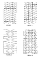
- FIG. 3 shows an example of a conventional layout of transparent tracks for linking the electrodes on the edge.
- the transparent zone 6 also known as the sensitive surface
- linking tracks between the electrodes and the connecting tracks 5 are transparent tracks
- the connecting tracks 5 in the access zone are made from metal.
- This figure shows that certain transparent linking tracks 7 are situated on the sensitive surface but outside the electrodes. That is to say that these transparent tracks are located between the last electrodes of the top of the detection surface and the access zone which is generally opaque.
- This arrangement of tracks increases the failure of detection of the position of an object in these zones.
- the use of electrodes up to the physical edge of the sensitive surface makes it possible to obtain more efficient signal processing in order to determine the position of an object.
- the presence of a linking track at the edge of the sensitive surface tends to complicate the signal processing and to degrade the precision of detection of the object.
- FIG. 4 shows a touch screen according to the invention.
- the transparent edge tracks 7 of FIG. 3 have disappeared, having been displaced inwards as linking tracks 8 between two rows of electrodes.
- the electrodes of the last row constitute the border with the access zone around the zone of electrodes.
- FIG. 5 a has the same elements as FIG. 1 b , but a new guard G 2 is introduced above the connecting tracks PT such that these connecting tracks are placed in a sandwich between the guard G 1 (corresponding to the guard G in FIG. 1 b ) and the guard G 2 which are at the same guard potential, particularly linked together electrically.
- These connecting tracks PT can be covered with a dielectric then with a layer of metal (metal guard) or with the transparent conductive ITO layer (transparent guard) linked to the guard potential by the flexible link CF.
- metal guard metal guard
- transparent guard transparent guard
- FIG. 5 b shows an embodiment in which linking tracks PL make it possible to link the conductive connecting tracks PT to electrodes E arranged on a surface having electrodes.
- the electrodes are transparent and made from ITO material.
- the linking tracks PL are transparent when they are in the detection zone corresponding to the detection surface SD. They can be made from metal in the access zone. In the access zone, the connecting tracks PT are arranged, without contact, in a sandwich between a guard G 2 below and a guard G 3 above.
- the guards G 2 and G 3 are preferably made from metal, but can also be made from transparent ITO material.
- the guard G 2 can be an extension of the guard G 1 provided for the electrodes E. According to the invention, it is provided to replace the guard G 3 (placed above the connecting tracks) by (at least one) measurement electrode(s). In fact, these electrodes like all the others can act as a guard for tracks located below them.
- These electrodes, arranged on the side of the device can serve mainly for edge detection, i.e. the detection of an object, such as the fingers, placed on the edge of the device.
- FIG. 6 shows the general solution in a top view with the metal tracks 5 situated between two guards G 1 and G 2 . Any track on the edges has been dispensed with.
- the flexible connectors CF are also arranged between G 1 and G 2 . All the transparent tracks 8 in the transparent zone 6 are situated between two rows of electrodes.
- the invention it is possible for example to detect the four fingers (at least two fingers) on one side of the device and the thumb on the other side, in order to deduce whether the device is held in the left or the right hand. According to whether this is right- or left-handed, all or some of the touch (icons), gestural or hovering commands can be repositioned in order to optimize the ergonomics.
- the zone the furthest from the fingers holding the device can also be found in order to optimize the scope for hovering. This latter mode is very sensitive to edge effects, and fingers at the edge considerably reduce the scope for hovering.
- the capacitive detection of the fingers or any object close to the touch screen can advantageously be done with individual electrodes protected on the screen side by a guard the potential of which is substantially equal to that of the electrodes as the measured capacitances are very low (up to a few fF) and any unwanted parasitic leakage capacitance would degrade the detection.
- the electronics manages each electrode so as to measure each inter electrode-object capacitance.
- the objects detected are referenced at the earth potential of the electronics.
- Electrodes can also be placed on the sides of the portable device in order to increase the possibilities of detection of a close object.
- the shape of the object can also be detected such as for example a hand so as to know in which direction (front or back) the device is held in the hand.
- the device is placed on a flat surface such as a table or placed in a pocket of an item of clothing.
- FIG. 7 is a diagrammatic front view of a device according to the invention. It is noted that the guard G 2 is a frame around the entire transparent surface 6 . The guard G 1 , not shown in FIG. 6 , is arranged in a plane parallel to the guard G 2 so as to frame metal tracks.
- FIG. 8 shows another embodiment of the device according to the invention.
- the surface having electrodes is a rectangle for which the linking tracks 9 made from a transparent material link the electrodes from the surface to the access zones 10 and 11 on the short sides of the rectangle.
- the guards G 1 and G 2 are arranged in a sandwich in these access zones.
- In each access zone is an integrated circuit IC 1 , IC 2 , connected to the linking tracks originating from the closest electrodes.
- the tracks between the transparent surface and the integrated circuits can be made from metal.
- This solution makes it possible to avoid placing conductive connecting tracks on the long sides that are used for the greater part of the time for holding the device.
- the advantage is dispensing with the long tracks on the vertical sides.
- a few conductive connecting tracks 12 are used on the vertical sides so that the two integrated circuits can intercommunicate. But these tracks 12 have no need to be guarded.
- the two integrated circuits can use the same guard potential.
- the integrated circuit IC 2 is then linked to a processing unit via the ribbon cable CF.
- the electrodes preferably cover as much as possible of the sensitive surface of the touch screen.
- the electrodes can have a more complex form than a rectangle, as can be seen in FIGS. 9 to 12 .
- triangular or concave electrodes can make it possible to reduce their number to the maximum while keeping the same detection performance (precision). It is possible in fact to use triangular shapes in order to add an item of measurement information by using the changing geometry of each electrode with respect to the position of the object.
- the interleaved concave electrodes nested together can make it possible to reduce failure by sudden rupture during the passage of an object from one electrode to another or to add information by using the changing geometry of each electrode with respect to the position of the object.
Landscapes
- Engineering & Computer Science (AREA)
- General Engineering & Computer Science (AREA)
- Theoretical Computer Science (AREA)
- Human Computer Interaction (AREA)
- Physics & Mathematics (AREA)
- General Physics & Mathematics (AREA)
- Position Input By Displaying (AREA)
- User Interface Of Digital Computer (AREA)
- Telephone Function (AREA)
Applications Claiming Priority (3)
| Application Number | Priority Date | Filing Date | Title |
|---|---|---|---|
| FR1253820A FR2990020B1 (fr) | 2012-04-25 | 2012-04-25 | Dispositif de detection capacitive avec arrangement de pistes de liaison, et procede mettant en oeuvre un tel dispositif. |
| FR1253820 | 2012-04-25 | ||
| PCT/EP2013/057900 WO2013160151A1 (fr) | 2012-04-25 | 2013-04-16 | Dispositif de detection capacitive avec arrangement de pistes de liaison, et procede mettant en oeuvre un tel dispositif |
Publications (2)
| Publication Number | Publication Date |
|---|---|
| US20150035792A1 US20150035792A1 (en) | 2015-02-05 |
| US9104283B2 true US9104283B2 (en) | 2015-08-11 |
Family
ID=48326258
Family Applications (2)
| Application Number | Title | Priority Date | Filing Date |
|---|---|---|---|
| US14/115,008 Active US9104283B2 (en) | 2012-04-25 | 2013-04-16 | Capacitive detection device with arrangement of linking tracks, and method implementing such a device |
| US14/396,599 Abandoned US20150091854A1 (en) | 2012-04-25 | 2013-04-24 | Method for interacting with an apparatus implementing a capacitive control surface, interface and apparatus implementing this method |
Family Applications After (1)
| Application Number | Title | Priority Date | Filing Date |
|---|---|---|---|
| US14/396,599 Abandoned US20150091854A1 (en) | 2012-04-25 | 2013-04-24 | Method for interacting with an apparatus implementing a capacitive control surface, interface and apparatus implementing this method |
Country Status (7)
| Country | Link |
|---|---|
| US (2) | US9104283B2 (ko) |
| EP (3) | EP2842018A1 (ko) |
| JP (3) | JP6463669B2 (ko) |
| KR (2) | KR102028783B1 (ko) |
| CN (3) | CN106933417A (ko) |
| FR (2) | FR2990020B1 (ko) |
| WO (2) | WO2013160151A1 (ko) |
Cited By (12)
| Publication number | Priority date | Publication date | Assignee | Title |
|---|---|---|---|---|
| US20140360854A1 (en) * | 2011-12-21 | 2014-12-11 | Nanotec Solution | Pressure-sensitive capacitive measurement device and method for touch-sensitive and contactless interfaces |
| US20160188038A1 (en) * | 2013-05-17 | 2016-06-30 | Fogale Nanotech | Capacitive control interface device and method adapted for the implementation of highly resistive measurement electrodes |
| US20170024124A1 (en) * | 2014-04-14 | 2017-01-26 | Sharp Kabushiki Kaisha | Input device, and method for controlling input device |
| US10037118B2 (en) | 2012-04-30 | 2018-07-31 | Apple Inc. | Wide dynamic range capacitive sensing |
| US10318032B2 (en) | 2015-02-04 | 2019-06-11 | Quickstep Technologies Llc | Multilayer capacitive detection device, and apparatus comprising the device |
| US10372282B2 (en) | 2016-12-01 | 2019-08-06 | Apple Inc. | Capacitive coupling reduction in touch sensor panels |
| US10429974B2 (en) | 2016-09-23 | 2019-10-01 | Apple Inc. | Touch sensor panel with top and/or bottom shielding |
| US10474287B2 (en) | 2007-01-03 | 2019-11-12 | Apple Inc. | Double-sided touch-sensitive panel with shield and drive combined layer |
| US10521049B2 (en) * | 2017-09-29 | 2019-12-31 | Apple Inc. | Multi-via structures for touchscreens |
| US20200368924A1 (en) * | 2017-08-10 | 2020-11-26 | Fogale Nanotech | Capacitive casing element for robot, robot provided with such a casing element |
| US11010000B2 (en) * | 2018-06-29 | 2021-05-18 | Canon Kabushiki Kaisha | Electronic equipment having a touch operating member that can be operated while viewing display monitors |
| US11460964B2 (en) | 2011-10-20 | 2022-10-04 | Apple Inc. | Opaque thin film passivation |
Families Citing this family (25)
| Publication number | Priority date | Publication date | Assignee | Title |
|---|---|---|---|---|
| US8381135B2 (en) | 2004-07-30 | 2013-02-19 | Apple Inc. | Proximity detector in handheld device |
| FR2949007B1 (fr) | 2009-08-07 | 2012-06-08 | Nanotec Solution | Dispositif et procede d'interface de commande sensible a un mouvement d'un corps ou d'un objet et equipement de commande integrant ce dispositif. |
| FR2971066B1 (fr) | 2011-01-31 | 2013-08-23 | Nanotec Solution | Interface homme-machine tridimensionnelle. |
| FR2976688B1 (fr) | 2011-06-16 | 2021-04-23 | Nanotec Solution | Dispositif et procede pour generer une alimentation electrique dans un systeme electronique avec un potentiel de reference variable. |
| FR2985049B1 (fr) | 2011-12-22 | 2014-01-31 | Nanotec Solution | Dispositif de mesure capacitive a electrodes commutees pour interfaces tactiles et sans contact |
| FR2988176B1 (fr) | 2012-03-13 | 2014-11-21 | Nanotec Solution | Procede de mesure capacitive entre un objet et un plan d’electrodes par demodulation synchrone partielle |
| FR2988175B1 (fr) | 2012-03-13 | 2014-04-11 | Nanotec Solution | Procede de mesure capacitive par des electrodes non-regulieres, et appareil mettant en œuvre un tel procede |
| FR3002052B1 (fr) | 2013-02-14 | 2016-12-09 | Fogale Nanotech | Procede et dispositif pour naviguer dans un ecran d'affichage et appareil comprenant une telle navigation |
| FR3003964B1 (fr) | 2013-04-02 | 2016-08-26 | Fogale Nanotech | Dispositif pour interagir, sans contact, avec un appareil electronique et/ou informatique, et appareil equipe d'un tel dispositif |
| FR3004551A1 (fr) | 2013-04-15 | 2014-10-17 | Fogale Nanotech | Procede de detection capacitif multizone, dispositif et appareil mettant en oeuvre le procede |
| FR3013472B1 (fr) | 2013-11-19 | 2016-07-08 | Fogale Nanotech | Dispositif accessoire couvrant pour un appareil portable electronique et/ou informatique, et appareil equipe d'un tel dispositif accessoire |
| GB2521835A (en) | 2014-01-02 | 2015-07-08 | Nokia Technologies Oy | Electromagnetic shielding |
| FR3017723B1 (fr) | 2014-02-19 | 2017-07-21 | Fogale Nanotech | Procede d'interaction homme-machine par combinaison de commandes tactiles et sans contact |
| FR3019320B1 (fr) | 2014-03-28 | 2017-12-15 | Fogale Nanotech | Dispositif electronique de type montre-bracelet avec interface de commande sans contact et procede de controle d'un tel dispositif |
| KR101621277B1 (ko) | 2014-08-19 | 2016-05-16 | 크루셜텍 (주) | 터치 검출 장치 |
| WO2016028081A2 (ko) * | 2014-08-19 | 2016-02-25 | 크루셜텍(주) | 터치 검출 장치 |
| FR3025623B1 (fr) | 2014-09-05 | 2017-12-15 | Fogale Nanotech | Dispositif d'interface de commande et capteur d'empreintes digitales |
| FR3028061B1 (fr) * | 2014-10-29 | 2016-12-30 | Fogale Nanotech | Dispositif capteur capacitif comprenant des electrodes ajourees |
| FR3033203B1 (fr) * | 2015-02-27 | 2018-03-23 | Quickstep Technologies Llc | Procede pour interagir avec un appareil electronique et/ou informatique mettant en œuvre une surface de commande capacitive et une surface peripherique, interface et appareil mettant en œuvre ce procede |
| CN105573545A (zh) * | 2015-11-27 | 2016-05-11 | 努比亚技术有限公司 | 一种手势校准方法、装置及手势输入处理方法 |
| FR3051266B1 (fr) * | 2016-05-12 | 2019-07-05 | Fogale Nanotech | Dispositif d'interface capacitive a structure d'electrodes mixtes, et appareil comprenant le dispositif |
| FR3072176B1 (fr) * | 2017-10-10 | 2022-03-04 | Fogale Nanotech | Dispositif de mesure d'impedance |
| CN108062181B (zh) * | 2018-01-02 | 2021-08-17 | 京东方科技集团股份有限公司 | 基板及其制作方法、电子设备 |
| US11789561B2 (en) | 2021-09-24 | 2023-10-17 | Apple Inc. | Architecture for differential drive and sense touch technology |
| US11861084B2 (en) * | 2021-11-18 | 2024-01-02 | International Business Machines Corporation | Splitting a mobile device display and mapping content with single hand |
Citations (10)
| Publication number | Priority date | Publication date | Assignee | Title |
|---|---|---|---|---|
| FR2756048A1 (fr) | 1996-11-15 | 1998-05-22 | Nanotec Ingenierie | Pont de mesure capacitif flottant et systeme de mesure multi-capacitif associe |
| WO2004023067A2 (fr) | 2002-09-06 | 2004-03-18 | Nanotec Solution | Detecteur de proximite par capteur capacitif |
| WO2007060324A1 (fr) | 2005-11-24 | 2007-05-31 | Nanotec Solution | Dispositif et procede de mesure capacitive par pont flottant |
| US20100123681A1 (en) * | 2008-11-19 | 2010-05-20 | Au Optronics Corporation | Touch panel and touch display panel |
| US20100201647A1 (en) | 2009-02-11 | 2010-08-12 | Tpo Displays Corp. | Capacitive touch sensor |
| US20110216018A1 (en) * | 2010-03-05 | 2011-09-08 | Samsung Mobile Display Co., Ltd. | Flat panel display integrated with touch screen panel |
| US20110234491A1 (en) * | 2010-03-26 | 2011-09-29 | Nokia Corporation | Apparatus and method for proximity based input |
| EP2392994A1 (en) | 2009-08-12 | 2011-12-07 | Inferpoint Systems Limited | Active touch control system |
| US20120008266A1 (en) | 2009-07-29 | 2012-01-12 | Alps Electric Co., Ltd. | Operation device |
| US8829926B2 (en) * | 2012-11-19 | 2014-09-09 | Zrro Technologies (2009) Ltd. | Transparent proximity sensor |
Family Cites Families (45)
| Publication number | Priority date | Publication date | Assignee | Title |
|---|---|---|---|---|
| US7911456B2 (en) * | 1992-06-08 | 2011-03-22 | Synaptics Incorporated | Object position detector with edge motion feature and gesture recognition |
| US7663607B2 (en) * | 2004-05-06 | 2010-02-16 | Apple Inc. | Multipoint touchscreen |
| JP2001127866A (ja) * | 1999-10-27 | 2001-05-11 | Toshiba Corp | 通信端末 |
| US7088343B2 (en) * | 2001-04-30 | 2006-08-08 | Lenovo (Singapore) Pte., Ltd. | Edge touchpad input device |
| KR100980902B1 (ko) * | 2002-05-16 | 2010-09-07 | 소니 주식회사 | 입력 방법 및 입력 장치 |
| JP2004302734A (ja) * | 2003-03-31 | 2004-10-28 | Mitsubishi Electric Corp | 情報端末並びにその動作切替えをコンピュータに実行させるプログラム |
| JP2006140700A (ja) * | 2004-11-11 | 2006-06-01 | Canon Inc | デジタルカメラ |
| JP2007122326A (ja) * | 2005-10-27 | 2007-05-17 | Alps Electric Co Ltd | 入力装置および前記入力装置を使用した電子機器 |
| US7657849B2 (en) * | 2005-12-23 | 2010-02-02 | Apple Inc. | Unlocking a device by performing gestures on an unlock image |
| JP2009055238A (ja) * | 2007-08-24 | 2009-03-12 | Ntt Docomo Inc | 携帯端末および起動方法 |
| US8633915B2 (en) * | 2007-10-04 | 2014-01-21 | Apple Inc. | Single-layer touch-sensitive display |
| CN101952792B (zh) * | 2007-11-19 | 2014-07-02 | 瑟克公司 | 与显示器结合且具有接近及触摸感应能力的触摸板 |
| CN101470555A (zh) * | 2007-12-25 | 2009-07-01 | 义隆电子股份有限公司 | 具有防误感功能的触控面板 |
| TWI401596B (zh) * | 2007-12-26 | 2013-07-11 | Elan Microelectronics Corp | 觸控螢幕的座標校準方法 |
| TWM348999U (en) * | 2008-02-18 | 2009-01-11 | Tpk Touch Solutions Inc | Capacitive touch panel |
| US20110020517A1 (en) * | 2008-04-04 | 2011-01-27 | Mark Rubin | Taste modifying product |
| TW201025108A (en) * | 2008-12-31 | 2010-07-01 | Acrosense Technology Co Ltd | Capacitive touch panel |
| CN101477430B (zh) * | 2009-01-16 | 2012-11-07 | 汕头超声显示器(二厂)有限公司 | 一种电容式触摸屏 |
| JP5337061B2 (ja) * | 2009-02-20 | 2013-11-06 | セイコーインスツル株式会社 | タッチパネル及びこれを備える表示装置 |
| JP2010262557A (ja) * | 2009-05-11 | 2010-11-18 | Sony Corp | 情報処理装置および方法 |
| JP2011044933A (ja) * | 2009-08-21 | 2011-03-03 | Nec Saitama Ltd | 携帯電話機および制限解除方法 |
| US8441460B2 (en) * | 2009-11-24 | 2013-05-14 | Mediatek Inc. | Apparatus and method for providing side touch panel as part of man-machine interface (MMI) |
| JP5476952B2 (ja) * | 2009-12-03 | 2014-04-23 | 日本電気株式会社 | 携帯端末 |
| CN101719038B (zh) * | 2009-12-30 | 2011-06-15 | 友达光电股份有限公司 | 触控显示面板以及触控基板 |
| US8799827B2 (en) * | 2010-02-19 | 2014-08-05 | Microsoft Corporation | Page manipulations using on and off-screen gestures |
| US9274682B2 (en) * | 2010-02-19 | 2016-03-01 | Microsoft Technology Licensing, Llc | Off-screen gestures to create on-screen input |
| JP5264800B2 (ja) * | 2010-02-23 | 2013-08-14 | パナソニック株式会社 | タッチパネル装置 |
| CN102193226A (zh) * | 2010-03-17 | 2011-09-21 | 谊达光电科技股份有限公司 | 具近接感应功能的面板 |
| JP2011198009A (ja) * | 2010-03-19 | 2011-10-06 | Sony Corp | 入力機能付き電気光学装置 |
| CN102375633A (zh) * | 2010-08-25 | 2012-03-14 | 毅齐科技股份有限公司 | 一种表面电容式触控面板的多点触控结构及其方法 |
| JP2012065107A (ja) * | 2010-09-15 | 2012-03-29 | Kyocera Corp | 携帯端末装置 |
| TW201214237A (en) * | 2010-09-16 | 2012-04-01 | Asustek Comp Inc | Touch display device and control method thereof |
| ES2900188T3 (es) * | 2010-09-24 | 2022-03-16 | Huawei Tech Co Ltd | Dispositivo electrónico portátil y método para controlar el mismo |
| JP5616184B2 (ja) * | 2010-09-28 | 2014-10-29 | 株式会社ジャパンディスプレイ | タッチ検出機能付き表示装置および電子機器 |
| WO2012049942A1 (ja) * | 2010-10-13 | 2012-04-19 | Necカシオモバイルコミュニケーションズ株式会社 | 携帯端末装置、および携帯端末装置におけるタッチパネルの表示方法 |
| US9652089B2 (en) * | 2010-11-09 | 2017-05-16 | Tpk Touch Solutions Inc. | Touch panel stackup |
| JP2012194810A (ja) * | 2011-03-16 | 2012-10-11 | Kyocera Corp | 携帯電子機器、接触操作制御方法および接触操作制御プログラム |
| KR101706242B1 (ko) * | 2011-04-27 | 2017-02-14 | 엘지디스플레이 주식회사 | 인셀 터치 패널 |
| US9229489B2 (en) * | 2011-05-03 | 2016-01-05 | Facebook, Inc. | Adjusting mobile device state based on user intentions and/or identity |
| US20120299868A1 (en) * | 2011-05-25 | 2012-11-29 | Broadcom Corporation | High Noise Immunity and High Spatial Resolution Mutual Capacitive Touch Panel |
| US20130154955A1 (en) * | 2011-12-19 | 2013-06-20 | David Brent GUARD | Multi-Surface Touch Sensor Device With Mode of Operation Selection |
| US20130300668A1 (en) * | 2012-01-17 | 2013-11-14 | Microsoft Corporation | Grip-Based Device Adaptations |
| KR101859515B1 (ko) * | 2012-02-14 | 2018-05-21 | 삼성디스플레이 주식회사 | 터치 패널 |
| US20140078086A1 (en) * | 2012-09-20 | 2014-03-20 | Marvell World Trade Ltd. | Augmented touch control for hand-held devices |
| US9727235B2 (en) * | 2013-12-12 | 2017-08-08 | Lenovo (Singapore) Pte. Ltd. | Switching an interface mode using an input gesture |
-
2012
- 2012-04-25 FR FR1253820A patent/FR2990020B1/fr not_active Expired - Fee Related
-
2013
- 2013-04-16 FR FR1353417A patent/FR2990033B1/fr active Active
- 2013-04-16 US US14/115,008 patent/US9104283B2/en active Active
- 2013-04-16 CN CN201710145477.2A patent/CN106933417A/zh active Pending
- 2013-04-16 KR KR1020147030605A patent/KR102028783B1/ko active IP Right Grant
- 2013-04-16 EP EP13721285.8A patent/EP2842018A1/fr not_active Withdrawn
- 2013-04-16 CN CN201380021798.1A patent/CN104321726B/zh active Active
- 2013-04-16 WO PCT/EP2013/057900 patent/WO2013160151A1/fr active Application Filing
- 2013-04-16 JP JP2015507470A patent/JP6463669B2/ja not_active Expired - Fee Related
- 2013-04-24 EP EP13723682.4A patent/EP2842019B1/fr active Active
- 2013-04-24 EP EP16170975.3A patent/EP3079047B1/fr active Active
- 2013-04-24 JP JP2015507506A patent/JP2015519644A/ja active Pending
- 2013-04-24 KR KR1020147032573A patent/KR101875995B1/ko active IP Right Grant
- 2013-04-24 CN CN201380022039.7A patent/CN104335150B/zh active Active
- 2013-04-24 US US14/396,599 patent/US20150091854A1/en not_active Abandoned
- 2013-04-24 WO PCT/EP2013/058428 patent/WO2013160323A1/fr active Application Filing
-
2018
- 2018-01-19 JP JP2018007011A patent/JP2018063732A/ja active Pending
Patent Citations (11)
| Publication number | Priority date | Publication date | Assignee | Title |
|---|---|---|---|---|
| FR2756048A1 (fr) | 1996-11-15 | 1998-05-22 | Nanotec Ingenierie | Pont de mesure capacitif flottant et systeme de mesure multi-capacitif associe |
| WO2004023067A2 (fr) | 2002-09-06 | 2004-03-18 | Nanotec Solution | Detecteur de proximite par capteur capacitif |
| WO2007060324A1 (fr) | 2005-11-24 | 2007-05-31 | Nanotec Solution | Dispositif et procede de mesure capacitive par pont flottant |
| US20100123681A1 (en) * | 2008-11-19 | 2010-05-20 | Au Optronics Corporation | Touch panel and touch display panel |
| US20100201647A1 (en) | 2009-02-11 | 2010-08-12 | Tpo Displays Corp. | Capacitive touch sensor |
| US20120008266A1 (en) | 2009-07-29 | 2012-01-12 | Alps Electric Co., Ltd. | Operation device |
| EP2392994A1 (en) | 2009-08-12 | 2011-12-07 | Inferpoint Systems Limited | Active touch control system |
| US20120113038A1 (en) | 2009-08-12 | 2012-05-10 | Inferpoint Systems Limited | Active touch system |
| US20110216018A1 (en) * | 2010-03-05 | 2011-09-08 | Samsung Mobile Display Co., Ltd. | Flat panel display integrated with touch screen panel |
| US20110234491A1 (en) * | 2010-03-26 | 2011-09-29 | Nokia Corporation | Apparatus and method for proximity based input |
| US8829926B2 (en) * | 2012-11-19 | 2014-09-09 | Zrro Technologies (2009) Ltd. | Transparent proximity sensor |
Cited By (18)
| Publication number | Priority date | Publication date | Assignee | Title |
|---|---|---|---|---|
| US11112904B2 (en) | 2007-01-03 | 2021-09-07 | Apple Inc. | Double-sided touch-sensitive panel with shield and drive combined layer |
| US10474287B2 (en) | 2007-01-03 | 2019-11-12 | Apple Inc. | Double-sided touch-sensitive panel with shield and drive combined layer |
| US11460964B2 (en) | 2011-10-20 | 2022-10-04 | Apple Inc. | Opaque thin film passivation |
| US10396784B2 (en) * | 2011-12-21 | 2019-08-27 | Quickstep Technologies Llc | Pressure-sensitive capacitive measurement device and method for touch-sensitive and contactless interfaces |
| US20140360854A1 (en) * | 2011-12-21 | 2014-12-11 | Nanotec Solution | Pressure-sensitive capacitive measurement device and method for touch-sensitive and contactless interfaces |
| US10620765B2 (en) | 2012-04-30 | 2020-04-14 | Apple Inc. | Wide dynamic range capacitive sensing |
| US10037118B2 (en) | 2012-04-30 | 2018-07-31 | Apple Inc. | Wide dynamic range capacitive sensing |
| US9983746B2 (en) * | 2013-05-17 | 2018-05-29 | Quickstep Technologies Llc | Capacitive control interface device and method adapted to the implementation of highly resistive measurement electrodes |
| US20160188038A1 (en) * | 2013-05-17 | 2016-06-30 | Fogale Nanotech | Capacitive control interface device and method adapted for the implementation of highly resistive measurement electrodes |
| US20170024124A1 (en) * | 2014-04-14 | 2017-01-26 | Sharp Kabushiki Kaisha | Input device, and method for controlling input device |
| US10318032B2 (en) | 2015-02-04 | 2019-06-11 | Quickstep Technologies Llc | Multilayer capacitive detection device, and apparatus comprising the device |
| US10429974B2 (en) | 2016-09-23 | 2019-10-01 | Apple Inc. | Touch sensor panel with top and/or bottom shielding |
| US10955978B2 (en) | 2016-09-23 | 2021-03-23 | Apple Inc. | Touch sensor panel with top and/or bottom shielding |
| US10372282B2 (en) | 2016-12-01 | 2019-08-06 | Apple Inc. | Capacitive coupling reduction in touch sensor panels |
| US10606430B2 (en) | 2016-12-01 | 2020-03-31 | Apple Inc. | Capacitive coupling reduction in touch sensor panels |
| US20200368924A1 (en) * | 2017-08-10 | 2020-11-26 | Fogale Nanotech | Capacitive casing element for robot, robot provided with such a casing element |
| US10521049B2 (en) * | 2017-09-29 | 2019-12-31 | Apple Inc. | Multi-via structures for touchscreens |
| US11010000B2 (en) * | 2018-06-29 | 2021-05-18 | Canon Kabushiki Kaisha | Electronic equipment having a touch operating member that can be operated while viewing display monitors |
Also Published As
| Publication number | Publication date |
|---|---|
| EP3079047A1 (fr) | 2016-10-12 |
| EP2842019A1 (fr) | 2015-03-04 |
| US20150091854A1 (en) | 2015-04-02 |
| US20150035792A1 (en) | 2015-02-05 |
| WO2013160323A1 (fr) | 2013-10-31 |
| CN104335150A (zh) | 2015-02-04 |
| KR101875995B1 (ko) | 2018-07-06 |
| CN104335150B (zh) | 2019-02-22 |
| FR2990033A1 (fr) | 2013-11-01 |
| EP3079047B1 (fr) | 2017-09-27 |
| EP2842019B1 (fr) | 2016-05-25 |
| JP2015519644A (ja) | 2015-07-09 |
| FR2990020A1 (fr) | 2013-11-01 |
| JP2015518215A (ja) | 2015-06-25 |
| EP2842018A1 (fr) | 2015-03-04 |
| JP2018063732A (ja) | 2018-04-19 |
| KR20150010718A (ko) | 2015-01-28 |
| FR2990020B1 (fr) | 2014-05-16 |
| KR102028783B1 (ko) | 2019-10-04 |
| WO2013160151A1 (fr) | 2013-10-31 |
| CN104321726B (zh) | 2017-04-12 |
| JP6463669B2 (ja) | 2019-02-06 |
| CN106933417A (zh) | 2017-07-07 |
| FR2990033B1 (fr) | 2014-05-16 |
| CN104321726A (zh) | 2015-01-28 |
| KR20150010755A (ko) | 2015-01-28 |
Similar Documents
| Publication | Publication Date | Title |
|---|---|---|
| US9104283B2 (en) | Capacitive detection device with arrangement of linking tracks, and method implementing such a device | |
| KR102044083B1 (ko) | 터치 검출 장치 및 검출 방법, 그리고 터치 기기 | |
| US9870109B2 (en) | Device and method for localized force and proximity sensing | |
| US10025411B2 (en) | Touch screen and pressure touch detection method thereof | |
| KR102450301B1 (ko) | 중간 차폐 전극층을 채용한 포스 및 근접 센싱을 위한 디바이스 및 방법 | |
| US9690395B2 (en) | Digitizer system | |
| KR101996703B1 (ko) | 투명 가드 상에 금속 띠를 결합하는 용량성 센싱 장치 | |
| US8653834B2 (en) | Input device with floating electrodes having at least one aperture | |
| KR101114873B1 (ko) | 근접센서를 이용한 이동 감지장치 및 이동 감지방법 | |
| US9189093B2 (en) | System and method for the generation of a signal correlated with a manual input operation | |
| JP6369805B2 (ja) | タッチセンサ装置及び電子機器並びにタッチジェスチャー検知プログラム | |
| US20150185946A1 (en) | Touch surface having capacitive and resistive sensors | |
| US20100026655A1 (en) | Capacitive Touchscreen or Touchpad for Finger or Stylus | |
| CN103975297A (zh) | 输入接口、便携式电子装置以及制造输入接口的方法 | |
| JP2011501307A (ja) | 圧力センサーアレイを有するシングルタッチ型またはマルチタッチ型のタッチスクリーンまたはタッチパッド、および圧力センサーの製造方法 | |
| KR20160117719A (ko) | 터치 센서 장치 | |
| US9280233B1 (en) | Routing for touch sensor electrodes | |
| JP2014170334A (ja) | 静電容量式タッチパネルおよびそれを用いた手持ち式電子機器 | |
| KR20120094984A (ko) | 접촉 감지 패널 | |
| US9372587B2 (en) | Methods and apparatus for arranging electrode layers and associated routing traces in a sensor device | |
| KR101655429B1 (ko) | 3차원 터치 스크린 패널 | |
| KR101494259B1 (ko) | 복합터치 부가형 패널과 이를 이용한 터치 인식 방법 |
Legal Events
| Date | Code | Title | Description |
|---|---|---|---|
| AS | Assignment |
Owner name: FOGALE NANOTECH, FRANCE Free format text: ASSIGNMENT OF ASSIGNORS INTEREST;ASSIGNORS:ROZIERE, DIDIER;BLONDIN, CHRISTOPHE;REEL/FRAME:031589/0702 Effective date: 20130514 |
|
| STCF | Information on status: patent grant |
Free format text: PATENTED CASE |
|
| FEPP | Fee payment procedure |
Free format text: PAT HOLDER NO LONGER CLAIMS SMALL ENTITY STATUS, ENTITY STATUS SET TO UNDISCOUNTED (ORIGINAL EVENT CODE: STOL); ENTITY STATUS OF PATENT OWNER: LARGE ENTITY |
|
| FEPP | Fee payment procedure |
Free format text: PAYOR NUMBER ASSIGNED (ORIGINAL EVENT CODE: ASPN); ENTITY STATUS OF PATENT OWNER: LARGE ENTITY |
|
| AS | Assignment |
Owner name: QUICKSTEP TECHNOLOGIES LLC, DELAWARE Free format text: ASSIGNMENT OF ASSIGNORS INTEREST;ASSIGNOR:FOGALE NANOTECH S.A.;REEL/FRAME:037552/0041 Effective date: 20151221 |
|
| MAFP | Maintenance fee payment |
Free format text: PAYMENT OF MAINTENANCE FEE, 4TH YEAR, LARGE ENTITY (ORIGINAL EVENT CODE: M1551); ENTITY STATUS OF PATENT OWNER: LARGE ENTITY Year of fee payment: 4 |
|
| MAFP | Maintenance fee payment |
Free format text: PAYMENT OF MAINTENANCE FEE, 8TH YEAR, LARGE ENTITY (ORIGINAL EVENT CODE: M1552); ENTITY STATUS OF PATENT OWNER: LARGE ENTITY Year of fee payment: 8 |