US9012883B2 - Recessed contact to semiconductor nanowires - Google Patents
Recessed contact to semiconductor nanowires Download PDFInfo
- Publication number
- US9012883B2 US9012883B2 US13/723,413 US201213723413A US9012883B2 US 9012883 B2 US9012883 B2 US 9012883B2 US 201213723413 A US201213723413 A US 201213723413A US 9012883 B2 US9012883 B2 US 9012883B2
- Authority
- US
- United States
- Prior art keywords
- semiconductor
- nanowires
- nanowire
- semiconductor nanowire
- top surface
- Prior art date
- Legal status (The legal status is an assumption and is not a legal conclusion. Google has not performed a legal analysis and makes no representation as to the accuracy of the status listed.)
- Expired - Fee Related, expires
Links
Images


Classifications
-
- H01L31/022466—
-
- H—ELECTRICITY
- H10—SEMICONDUCTOR DEVICES; ELECTRIC SOLID-STATE DEVICES NOT OTHERWISE PROVIDED FOR
- H10D—INORGANIC ELECTRIC SEMICONDUCTOR DEVICES
- H10D64/00—Electrodes of devices having potential barriers
- H10D64/20—Electrodes characterised by their shapes, relative sizes or dispositions
- H10D64/205—Nanosized electrodes, e.g. nanowire electrodes
-
- H—ELECTRICITY
- H01—ELECTRIC ELEMENTS
- H01L—SEMICONDUCTOR DEVICES NOT COVERED BY CLASS H10
- H01L21/00—Processes or apparatus adapted for the manufacture or treatment of semiconductor or solid state devices or of parts thereof
- H01L21/02—Manufacture or treatment of semiconductor devices or of parts thereof
- H01L21/02104—Forming layers
- H01L21/02107—Forming insulating materials on a substrate
- H01L21/02109—Forming insulating materials on a substrate characterised by the type of layer, e.g. type of material, porous/non-porous, pre-cursors, mixtures or laminates
- H01L21/02112—Forming insulating materials on a substrate characterised by the type of layer, e.g. type of material, porous/non-porous, pre-cursors, mixtures or laminates characterised by the material of the layer
- H01L21/02123—Forming insulating materials on a substrate characterised by the type of layer, e.g. type of material, porous/non-porous, pre-cursors, mixtures or laminates characterised by the material of the layer the material containing silicon
- H01L21/02164—Forming insulating materials on a substrate characterised by the type of layer, e.g. type of material, porous/non-porous, pre-cursors, mixtures or laminates characterised by the material of the layer the material containing silicon the material being a silicon oxide, e.g. SiO2
-
- H—ELECTRICITY
- H01—ELECTRIC ELEMENTS
- H01L—SEMICONDUCTOR DEVICES NOT COVERED BY CLASS H10
- H01L21/00—Processes or apparatus adapted for the manufacture or treatment of semiconductor or solid state devices or of parts thereof
- H01L21/02—Manufacture or treatment of semiconductor devices or of parts thereof
- H01L21/02104—Forming layers
- H01L21/02107—Forming insulating materials on a substrate
- H01L21/02109—Forming insulating materials on a substrate characterised by the type of layer, e.g. type of material, porous/non-porous, pre-cursors, mixtures or laminates
- H01L21/02205—Forming insulating materials on a substrate characterised by the type of layer, e.g. type of material, porous/non-porous, pre-cursors, mixtures or laminates the layer being characterised by the precursor material for deposition
- H01L21/02208—Forming insulating materials on a substrate characterised by the type of layer, e.g. type of material, porous/non-porous, pre-cursors, mixtures or laminates the layer being characterised by the precursor material for deposition the precursor containing a compound comprising Si
- H01L21/02214—Forming insulating materials on a substrate characterised by the type of layer, e.g. type of material, porous/non-porous, pre-cursors, mixtures or laminates the layer being characterised by the precursor material for deposition the precursor containing a compound comprising Si the compound comprising silicon and oxygen
-
- H—ELECTRICITY
- H01—ELECTRIC ELEMENTS
- H01L—SEMICONDUCTOR DEVICES NOT COVERED BY CLASS H10
- H01L21/00—Processes or apparatus adapted for the manufacture or treatment of semiconductor or solid state devices or of parts thereof
- H01L21/02—Manufacture or treatment of semiconductor devices or of parts thereof
- H01L21/02104—Forming layers
- H01L21/02107—Forming insulating materials on a substrate
- H01L21/02225—Forming insulating materials on a substrate characterised by the process for the formation of the insulating layer
- H01L21/0226—Forming insulating materials on a substrate characterised by the process for the formation of the insulating layer formation by a deposition process
- H01L21/02263—Forming insulating materials on a substrate characterised by the process for the formation of the insulating layer formation by a deposition process deposition from the gas or vapour phase
- H01L21/02271—Forming insulating materials on a substrate characterised by the process for the formation of the insulating layer formation by a deposition process deposition from the gas or vapour phase deposition by decomposition or reaction of gaseous or vapour phase compounds, i.e. chemical vapour deposition
- H01L21/0228—Forming insulating materials on a substrate characterised by the process for the formation of the insulating layer formation by a deposition process deposition from the gas or vapour phase deposition by decomposition or reaction of gaseous or vapour phase compounds, i.e. chemical vapour deposition deposition by cyclic CVD, e.g. ALD, ALE, pulsed CVD
-
- H—ELECTRICITY
- H01—ELECTRIC ELEMENTS
- H01L—SEMICONDUCTOR DEVICES NOT COVERED BY CLASS H10
- H01L21/00—Processes or apparatus adapted for the manufacture or treatment of semiconductor or solid state devices or of parts thereof
- H01L21/02—Manufacture or treatment of semiconductor devices or of parts thereof
- H01L21/02104—Forming layers
- H01L21/02365—Forming inorganic semiconducting materials on a substrate
- H01L21/02518—Deposited layers
- H01L21/02587—Structure
- H01L21/0259—Microstructure
- H01L21/02603—Nanowires
-
- H—ELECTRICITY
- H01—ELECTRIC ELEMENTS
- H01L—SEMICONDUCTOR DEVICES NOT COVERED BY CLASS H10
- H01L21/00—Processes or apparatus adapted for the manufacture or treatment of semiconductor or solid state devices or of parts thereof
- H01L21/02—Manufacture or treatment of semiconductor devices or of parts thereof
- H01L21/04—Manufacture or treatment of semiconductor devices or of parts thereof the devices having potential barriers, e.g. a PN junction, depletion layer or carrier concentration layer
- H01L21/18—Manufacture or treatment of semiconductor devices or of parts thereof the devices having potential barriers, e.g. a PN junction, depletion layer or carrier concentration layer the devices having semiconductor bodies comprising elements of Group IV of the Periodic Table or AIIIBV compounds with or without impurities, e.g. doping materials
- H01L21/30—Treatment of semiconductor bodies using processes or apparatus not provided for in groups H01L21/20 - H01L21/26
- H01L21/31—Treatment of semiconductor bodies using processes or apparatus not provided for in groups H01L21/20 - H01L21/26 to form insulating layers thereon, e.g. for masking or by using photolithographic techniques; After treatment of these layers; Selection of materials for these layers
- H01L21/3105—After-treatment
- H01L21/311—Etching the insulating layers by chemical or physical means
- H01L21/31105—Etching inorganic layers
- H01L21/31111—Etching inorganic layers by chemical means
- H01L21/31116—Etching inorganic layers by chemical means by dry-etching
-
- H01L33/16—
-
- H01L33/38—
-
- H01L33/385—
-
- H01L33/42—
-
- H—ELECTRICITY
- H10—SEMICONDUCTOR DEVICES; ELECTRIC SOLID-STATE DEVICES NOT OTHERWISE PROVIDED FOR
- H10D—INORGANIC ELECTRIC SEMICONDUCTOR DEVICES
- H10D62/00—Semiconductor bodies, or regions thereof, of devices having potential barriers
- H10D62/10—Shapes, relative sizes or dispositions of the regions of the semiconductor bodies; Shapes of the semiconductor bodies
- H10D62/117—Shapes of semiconductor bodies
- H10D62/118—Nanostructure semiconductor bodies
- H10D62/119—Nanowire, nanosheet or nanotube semiconductor bodies
- H10D62/122—Nanowire, nanosheet or nanotube semiconductor bodies oriented at angles to substrates, e.g. perpendicular to substrates
-
- H—ELECTRICITY
- H10—SEMICONDUCTOR DEVICES; ELECTRIC SOLID-STATE DEVICES NOT OTHERWISE PROVIDED FOR
- H10F—INORGANIC SEMICONDUCTOR DEVICES SENSITIVE TO INFRARED RADIATION, LIGHT, ELECTROMAGNETIC RADIATION OF SHORTER WAVELENGTH OR CORPUSCULAR RADIATION
- H10F10/00—Individual photovoltaic cells, e.g. solar cells
- H10F10/10—Individual photovoltaic cells, e.g. solar cells having potential barriers
- H10F10/16—Photovoltaic cells having only PN heterojunction potential barriers
- H10F10/163—Photovoltaic cells having only PN heterojunction potential barriers comprising only Group III-V materials, e.g. GaAs/AlGaAs or InP/GaInAs photovoltaic cells
-
- H—ELECTRICITY
- H10—SEMICONDUCTOR DEVICES; ELECTRIC SOLID-STATE DEVICES NOT OTHERWISE PROVIDED FOR
- H10F—INORGANIC SEMICONDUCTOR DEVICES SENSITIVE TO INFRARED RADIATION, LIGHT, ELECTROMAGNETIC RADIATION OF SHORTER WAVELENGTH OR CORPUSCULAR RADIATION
- H10F19/00—Integrated devices, or assemblies of multiple devices, comprising at least one photovoltaic cell covered by group H10F10/00, e.g. photovoltaic modules
-
- H—ELECTRICITY
- H10—SEMICONDUCTOR DEVICES; ELECTRIC SOLID-STATE DEVICES NOT OTHERWISE PROVIDED FOR
- H10F—INORGANIC SEMICONDUCTOR DEVICES SENSITIVE TO INFRARED RADIATION, LIGHT, ELECTROMAGNETIC RADIATION OF SHORTER WAVELENGTH OR CORPUSCULAR RADIATION
- H10F71/00—Manufacture or treatment of devices covered by this subclass
- H10F71/127—The active layers comprising only Group III-V materials, e.g. GaAs or InP
- H10F71/1276—The active layers comprising only Group III-V materials, e.g. GaAs or InP comprising growth substrates not made of Group III-V materials
-
- H—ELECTRICITY
- H10—SEMICONDUCTOR DEVICES; ELECTRIC SOLID-STATE DEVICES NOT OTHERWISE PROVIDED FOR
- H10F—INORGANIC SEMICONDUCTOR DEVICES SENSITIVE TO INFRARED RADIATION, LIGHT, ELECTROMAGNETIC RADIATION OF SHORTER WAVELENGTH OR CORPUSCULAR RADIATION
- H10F77/00—Constructional details of devices covered by this subclass
- H10F77/10—Semiconductor bodies
- H10F77/14—Shape of semiconductor bodies; Shapes, relative sizes or dispositions of semiconductor regions within semiconductor bodies
- H10F77/143—Shape of semiconductor bodies; Shapes, relative sizes or dispositions of semiconductor regions within semiconductor bodies comprising quantum structures
- H10F77/1437—Quantum wires or nanorods
-
- H—ELECTRICITY
- H10—SEMICONDUCTOR DEVICES; ELECTRIC SOLID-STATE DEVICES NOT OTHERWISE PROVIDED FOR
- H10F—INORGANIC SEMICONDUCTOR DEVICES SENSITIVE TO INFRARED RADIATION, LIGHT, ELECTROMAGNETIC RADIATION OF SHORTER WAVELENGTH OR CORPUSCULAR RADIATION
- H10F77/00—Constructional details of devices covered by this subclass
- H10F77/20—Electrodes
- H10F77/244—Electrodes made of transparent conductive layers, e.g. transparent conductive oxide [TCO] layers
-
- H—ELECTRICITY
- H10—SEMICONDUCTOR DEVICES; ELECTRIC SOLID-STATE DEVICES NOT OTHERWISE PROVIDED FOR
- H10H—INORGANIC LIGHT-EMITTING SEMICONDUCTOR DEVICES HAVING POTENTIAL BARRIERS
- H10H20/00—Individual inorganic light-emitting semiconductor devices having potential barriers, e.g. light-emitting diodes [LED]
- H10H20/80—Constructional details
- H10H20/81—Bodies
- H10H20/817—Bodies characterised by the crystal structures or orientations, e.g. polycrystalline, amorphous or porous
-
- H—ELECTRICITY
- H10—SEMICONDUCTOR DEVICES; ELECTRIC SOLID-STATE DEVICES NOT OTHERWISE PROVIDED FOR
- H10H—INORGANIC LIGHT-EMITTING SEMICONDUCTOR DEVICES HAVING POTENTIAL BARRIERS
- H10H20/00—Individual inorganic light-emitting semiconductor devices having potential barriers, e.g. light-emitting diodes [LED]
- H10H20/80—Constructional details
- H10H20/83—Electrodes
- H10H20/831—Electrodes characterised by their shape
- H10H20/8314—Electrodes characterised by their shape extending at least partially onto an outer side surface of the bodies
-
- H—ELECTRICITY
- H10—SEMICONDUCTOR DEVICES; ELECTRIC SOLID-STATE DEVICES NOT OTHERWISE PROVIDED FOR
- H10H—INORGANIC LIGHT-EMITTING SEMICONDUCTOR DEVICES HAVING POTENTIAL BARRIERS
- H10H20/00—Individual inorganic light-emitting semiconductor devices having potential barriers, e.g. light-emitting diodes [LED]
- H10H20/80—Constructional details
- H10H20/83—Electrodes
- H10H20/832—Electrodes characterised by their material
- H10H20/833—Transparent materials
-
- H—ELECTRICITY
- H01—ELECTRIC ELEMENTS
- H01L—SEMICONDUCTOR DEVICES NOT COVERED BY CLASS H10
- H01L21/00—Processes or apparatus adapted for the manufacture or treatment of semiconductor or solid state devices or of parts thereof
- H01L21/02—Manufacture or treatment of semiconductor devices or of parts thereof
- H01L21/04—Manufacture or treatment of semiconductor devices or of parts thereof the devices having potential barriers, e.g. a PN junction, depletion layer or carrier concentration layer
- H01L21/18—Manufacture or treatment of semiconductor devices or of parts thereof the devices having potential barriers, e.g. a PN junction, depletion layer or carrier concentration layer the devices having semiconductor bodies comprising elements of Group IV of the Periodic Table or AIIIBV compounds with or without impurities, e.g. doping materials
- H01L21/30—Treatment of semiconductor bodies using processes or apparatus not provided for in groups H01L21/20 - H01L21/26
- H01L21/31—Treatment of semiconductor bodies using processes or apparatus not provided for in groups H01L21/20 - H01L21/26 to form insulating layers thereon, e.g. for masking or by using photolithographic techniques; After treatment of these layers; Selection of materials for these layers
- H01L21/3205—Deposition of non-insulating-, e.g. conductive- or resistive-, layers on insulating layers; After-treatment of these layers
- H01L21/321—After treatment
- H01L21/3213—Physical or chemical etching of the layers, e.g. to produce a patterned layer from a pre-deposited extensive layer
- H01L21/32133—Physical or chemical etching of the layers, e.g. to produce a patterned layer from a pre-deposited extensive layer by chemical means only
- H01L21/32134—Physical or chemical etching of the layers, e.g. to produce a patterned layer from a pre-deposited extensive layer by chemical means only by liquid etching only
-
- H01L27/15—
-
- H—ELECTRICITY
- H01—ELECTRIC ELEMENTS
- H01L—SEMICONDUCTOR DEVICES NOT COVERED BY CLASS H10
- H01L2924/00—Indexing scheme for arrangements or methods for connecting or disconnecting semiconductor or solid-state bodies as covered by H01L24/00
-
- H—ELECTRICITY
- H01—ELECTRIC ELEMENTS
- H01L—SEMICONDUCTOR DEVICES NOT COVERED BY CLASS H10
- H01L2924/00—Indexing scheme for arrangements or methods for connecting or disconnecting semiconductor or solid-state bodies as covered by H01L24/00
- H01L2924/0001—Technical content checked by a classifier
- H01L2924/0002—Not covered by any one of groups H01L24/00, H01L24/00 and H01L2224/00
-
- H—ELECTRICITY
- H10—SEMICONDUCTOR DEVICES; ELECTRIC SOLID-STATE DEVICES NOT OTHERWISE PROVIDED FOR
- H10D—INORGANIC ELECTRIC SEMICONDUCTOR DEVICES
- H10D62/00—Semiconductor bodies, or regions thereof, of devices having potential barriers
- H10D62/80—Semiconductor bodies, or regions thereof, of devices having potential barriers characterised by the materials
- H10D62/85—Semiconductor bodies, or regions thereof, of devices having potential barriers characterised by the materials being Group III-V materials, e.g. GaAs
-
- H—ELECTRICITY
- H10—SEMICONDUCTOR DEVICES; ELECTRIC SOLID-STATE DEVICES NOT OTHERWISE PROVIDED FOR
- H10H—INORGANIC LIGHT-EMITTING SEMICONDUCTOR DEVICES HAVING POTENTIAL BARRIERS
- H10H29/00—Integrated devices, or assemblies of multiple devices, comprising at least one light-emitting semiconductor element covered by group H10H20/00
- H10H29/10—Integrated devices comprising at least one light-emitting semiconductor component covered by group H10H20/00
-
- Y—GENERAL TAGGING OF NEW TECHNOLOGICAL DEVELOPMENTS; GENERAL TAGGING OF CROSS-SECTIONAL TECHNOLOGIES SPANNING OVER SEVERAL SECTIONS OF THE IPC; TECHNICAL SUBJECTS COVERED BY FORMER USPC CROSS-REFERENCE ART COLLECTIONS [XRACs] AND DIGESTS
- Y02—TECHNOLOGIES OR APPLICATIONS FOR MITIGATION OR ADAPTATION AGAINST CLIMATE CHANGE
- Y02E—REDUCTION OF GREENHOUSE GAS [GHG] EMISSIONS, RELATED TO ENERGY GENERATION, TRANSMISSION OR DISTRIBUTION
- Y02E10/00—Energy generation through renewable energy sources
- Y02E10/50—Photovoltaic [PV] energy
- Y02E10/544—Solar cells from Group III-V materials
-
- Y—GENERAL TAGGING OF NEW TECHNOLOGICAL DEVELOPMENTS; GENERAL TAGGING OF CROSS-SECTIONAL TECHNOLOGIES SPANNING OVER SEVERAL SECTIONS OF THE IPC; TECHNICAL SUBJECTS COVERED BY FORMER USPC CROSS-REFERENCE ART COLLECTIONS [XRACs] AND DIGESTS
- Y02—TECHNOLOGIES OR APPLICATIONS FOR MITIGATION OR ADAPTATION AGAINST CLIMATE CHANGE
- Y02E—REDUCTION OF GREENHOUSE GAS [GHG] EMISSIONS, RELATED TO ENERGY GENERATION, TRANSMISSION OR DISTRIBUTION
- Y02E10/00—Energy generation through renewable energy sources
- Y02E10/50—Photovoltaic [PV] energy
- Y02E10/547—Monocrystalline silicon PV cells
-
- Y—GENERAL TAGGING OF NEW TECHNOLOGICAL DEVELOPMENTS; GENERAL TAGGING OF CROSS-SECTIONAL TECHNOLOGIES SPANNING OVER SEVERAL SECTIONS OF THE IPC; TECHNICAL SUBJECTS COVERED BY FORMER USPC CROSS-REFERENCE ART COLLECTIONS [XRACs] AND DIGESTS
- Y02—TECHNOLOGIES OR APPLICATIONS FOR MITIGATION OR ADAPTATION AGAINST CLIMATE CHANGE
- Y02P—CLIMATE CHANGE MITIGATION TECHNOLOGIES IN THE PRODUCTION OR PROCESSING OF GOODS
- Y02P70/00—Climate change mitigation technologies in the production process for final industrial or consumer products
- Y02P70/50—Manufacturing or production processes characterised by the final manufactured product
-
- Y—GENERAL TAGGING OF NEW TECHNOLOGICAL DEVELOPMENTS; GENERAL TAGGING OF CROSS-SECTIONAL TECHNOLOGIES SPANNING OVER SEVERAL SECTIONS OF THE IPC; TECHNICAL SUBJECTS COVERED BY FORMER USPC CROSS-REFERENCE ART COLLECTIONS [XRACs] AND DIGESTS
- Y10—TECHNICAL SUBJECTS COVERED BY FORMER USPC
- Y10S—TECHNICAL SUBJECTS COVERED BY FORMER USPC CROSS-REFERENCE ART COLLECTIONS [XRACs] AND DIGESTS
- Y10S977/00—Nanotechnology
- Y10S977/902—Specified use of nanostructure
- Y10S977/932—Specified use of nanostructure for electronic or optoelectronic application
Definitions
- the present invention relates to semiconductor devices and in particular to nanowire semiconductor devices.
- electrical contacts for axial nanowire devices are made by encapsulating the nanowires in an insulator and then etching the insulator to expose the tops of each wire. A conducting material is then deposited to make the electrical contacts to the nanowires.
- V oc average open circuit voltage
- InP solar cell 900 mV
- the spread in V oc is typically large, with a standard deviation of several 100 mV.
- nanowire solar cells with a higher open circuit voltage and a small spread in open circuit voltage are desired.
- An embodiment relates to a semiconductor nanowire device which includes at least one semiconductor nanowire having a bottom surface and a top surface, an insulating material which surrounds the semiconductor nanowire, and an electrode ohmically contacting the top surface of the semiconductor nanowire.
- a contact of the electrode to the semiconductor material of the semiconductor nanowire is dominated by the contact to the top surface of the semiconductor nanowire.
- Another embodiment relates to semiconductor nanowire device comprising at least one semiconductor nanowire having a bottom surface and a top surface, an insulating material which surrounds the semiconductor nanowire and extends above the top surface of the nanowire to create a recess between a sidewall of the insulating material and the top surface of the nanowire, and an electrode filling the recess and ohmically contacting the top surface of the nanowire.
- Another embodiment relates to a method of making a semiconductor nanowire device, comprising forming at least one semiconductor nanowire, the semiconductor nanowire having a catalyst particle on a top surface of the semiconductor nanowire or a sacrificial portion comprising the top surface, forming an insulating material around the semiconductor nanowire, removing the catalyst particle or the sacrificial portion to recess the top surface of the nanowire below a top surface of the insulating material, and forming an electrode in ohmic contact with the top surface of the nanowire.
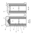
- FIGS. 1 a - 1 d are schematic diagrams illustrating (a) a prior art nanowire with a catalyst particle on top, partially covered with an insulator and fully covered with a transparent electrode, (b) a nanowire without a catalyst particle on top, partially covered with an insulator and fully covered with a transparent electrode, (c) a prior art nanowire with a catalyst particle on top, the full length of the nanowire and part of the catalyst particle covered with an insulator and fully covered with a transparent electrode and (d) a nanowire without a catalyst particle on top, the insulator extending beyond the top of the nanowire and fully covered with a transparent electrode.
- FIGS. 2 a - 2 b are schematic diagrams illustrating (a) the depletion regions of a nanowire of FIG. 1 a under low bias/low illumination conditions and (b) the depletion regions of a nanowire of FIG. 1 a under high bias/high illumination conditions.
- FIGS. 3 a - 3 d are (a) a circuit diagram of a nanowire device with nanowires of FIG. 1 b or 1 d connected in parallel, (b) a current versus voltage plot of the circuit of FIG. 3 a , (c) a circuit diagram of a nanowire device with nanowires of FIG. 1 a or 1 c connected in parallel and (d) a current versus voltage plot of the circuit of FIG. 3 c.
- FIGS. 4 a - 4 d are plots illustrating the increase in (a) efficiency, (b) fill factor, (c) open circuit voltage and (d) current density of embodiments versus conventional nanowire devices.
- FIGS. 5 a - 5 g are schematic diagrams illustrating a method of making a nanowire device according to an embodiment.
- FIGS. 5 h and 5 i are schematic side cross sectional view diagrams illustrating nanowire devices made according to alternative embodiments.
- FIGS. 6 a - 6 b are a scanning electron microscope (SEM) micrographs of (a) an array of nanowires with catalyst particles on top and (b) an array of nanowires with the catalyst particles removed, leaving recesses in the tops of the nanowires.
- SEM scanning electron microscope
- FIG. 7 is a plot of the reflectance as a function of wavelength comparing nanowires with and without gold catalyst particles on the tops of the nanowires.
- FIGS. 8 a - 8 b are schematic diagrams illustrating a method of making a nanowire device according to an alternative embodiment.
- nanowires are nanoscale structures that have a diameter (for cylindrical nanowires) or width (for non-cylindrical nanowires, such as nanowires having a hexagonal cross sectional shape in a plane perpendicular to its axis) less than 1 micron, such as 2-500 nm such as 100-300 nm.
- the length may be at least 0.5 microns, such as 0.5 to 3 microns, such as 1 to 2 microns.
- Efficient solar cells made from Group IV or III-V materials such as but not limited to Si, InP and GaAs, have the pn-junction very close to the top surface.
- the pn-junction is on the order of only a few 100 nm from the top of the surface.
- semiconductor nanowire devices Both modeling and experiment indicate that the most efficient semiconductor nanowire solar cells have a wire diameter of at least 180 nm.
- the semiconductor nanowire may be viewed as a small piece of planar material.
- the top contact preferably incorporates a transparent conducting oxide (TCO).
- TCO transparent conducting oxide
- the contact between the TCO and the active device preferably has as low resistance as possible, and is preferably ohmic.
- the contact itself not be optically active, i.e., the contact should not subtract from the open circuit voltage (V oc ) of the device.
- the conventional wisdom is that the Au seed particle is advantageous for forming an ohmic contact to the nanowires. Therefore, the Au particle is typically not removed, especially since removal would require additional processing steps.
- metal catalyst seed particles are known to reduce efficiency because of light shading. In addition to light shading and in contrast to conventional wisdom, an integrated metal particle may also provide poor electrical contact.
- Au has been found to make a Schottky-type contact to III-V semiconductors. The Schottky-type contact shows up in the current-voltage characteristics as a reverse diode in addition to any diode that may exist in the semiconductor nanowire. Therefore, the total device typically includes the semiconductor nanowire diode in series with a reverse Schottky diode as illustrated in FIG. 1 a and discussed in more detail below.
- FIGS. 1 a and 1 b illustrate nanowire devices of the prior art and of the first embodiment of the invention, respectively.
- the prior art semiconductor nanowire 101 is an axial nanowire which includes a first portion 102 having a first conductivity type (e.g., p-type or n-type) and a second portion 104 having a second conductivity type (e.g., n-type or p-type) different from the first conductivity type.
- a pn junction 103 is formed at the interface between the first portion 102 and the second portion 104 of the semiconductor nanowire 101 .
- the pn junction 103 has the electrical characteristics of a diode as indicated by the diode symbol 120 in the figure.
- the nanowire may comprise a p-i-n junction device in which the junction region 103 comprises an intrinsic semiconductor or semiconductor of the first or second conductivity type that has a dopant concentration that is at least an order of magnitude lower than that of regions 102 and 104 .
- an insulating or dielectric layer surrounds at least a portion of the sidewalls of the semiconductor nanowire 101 , thereby forming an insulating shell 108 around the semiconductor nanowire 101 .
- the insulating shell 108 is made of a transparent material, such as SiO 2 . If the semiconductor nanowire 101 is grown by the VLS process, or another process using metal catalyst particles, such as the AerotaxyTM process (as described in PCT Published Application WO 11/142,717 (the '717 publication), assigned to Qunano AB and hereby incorporated by reference in its entirety), the metal catalyst particle 106 is located on top of the second portion 104 of the semiconductor nanowire 101 .
- a reverse Schottky diode 122 may be formed between the metal catalyst particle 106 and the second portion 104 of the semiconductor nanowire 101 .
- the TCO electrode 110 encapsulates the semiconductor nanowire 101 , including the insulating shell 108 . In those portions of the semiconductor nanowire 101 that are not covered by the insulating shell 108 , direct contact may be made between the TCO electrode 110 and the semiconductor nanowire 101 . This contact is typically ohmic as illustrated by symbol 124 . An additional ohmic contact may be formed between the metal catalyst particle 106 and the TCO electrode 110 as indicated by symbol 126 .
- the ohmic contact connection 124 is in parallel with the gold particle-nanowire Schottky connection 122 . Alternatively, this contact may form another Schottky diode with different electrical characteristics from the diode 120 or the reverse Schottky diode 122 .
- FIGS. 2 a and 2 b schematically illustrate depletion regions 140 , 142 of a nanowire of FIG. 1 a under low bias/low illumination conditions ( FIG. 2 a ) and the depletion regions of a nanowire of FIG. 1 a under high bias/high illumination conditions ( FIG. 2 b ).
- a first depletion region 140 is formed at the pn junction 103 in the semiconductor nanowire 101 .
- a second depletion region 142 is formed due to the reverse Schottky diode 122 . That is, the reverse Schottky diode 122 induces a depletion region 142 in an upper portion of the semiconductor nanowire 101 .
- FIG. 2 a schematically illustrate depletion regions 140 , 142 of a nanowire of FIG. 1 a under low bias/low illumination conditions ( FIG. 2 a ) and the depletion regions of a nanowire of FIG. 1 a under high bias/high illumination conditions ( FIG. 2 b ).
- the thickness of the depletions regions 140 , 142 varies with the applied voltage and/or illumination.
- the reverse Schottky 122 diode may influence the contact on the nanowire side, making the contact dependent not only on process variations (e.g., ⁇ h 1 ) but possibly also on external forces.
- FIG. 1 b illustrates an embodiment in which the metal catalyst particle 106 is removed prior to depositing the TCO electrode 110 .
- an ohmic contact 128 is formed between the top surface of the semiconductor nanowire 101 and the TCO electrode 110 rather than the reverse Schottky diode 122 formed in the semiconductor nanowire 101 illustrated FIG. 1 a .
- the height between the top of the insulating shell 108 and the top surface 101 a of the semiconductor nanowire 101 is ⁇ h 1 , where ⁇ h 1 indicates the typical process variation for the length of the exposed length of nanowire tip.
- the semiconductor nanowire 101 has a diameter or width and the TCO electrode 110 contacts a side portion 101 b of the semiconductor nanowire 101 below the top surface 101 a such that the length ⁇ h 1 of the side portion 101 b is less than the diameter/width 101 c of the semiconductor nanowire 101 .
- diameter/width 101 c may be 10% to 500% greater, such as 50-100% greater than the length ⁇ h 1 of the side portion 101 b .
- ⁇ h 1 equals to zero and no side portion of the nanowire is exposed by the shell 108 , such that the nanowire and the shell have about the same height.
- the electrode 110 contacts only (exclusively) the top surface 101 a of the nanowire but not the side portion 101 b of the nanowire.
- a longer side portion 101 b of the nanowire is exposed than would otherwise be necessary so as not to accidentally leave some nanowires uncontacted.
- the top electrical contact/electrode 110 is formed, varying portions of the nanowire tips make contact with the electrode 101 . That is, the top electrode 110 is formed along longer side portions 101 b in the longer nanowires than in the shorter nanowires (where ⁇ h 1 may equal to zero in shorter nanowires and the electrode 110 only contacts the top surface 101 a ).
- the difference in the contact area between longer and shorter nanowires to the electrode 110 leads to undesirable non-uniformity in output and performance between different nanowires in the same device.
- FIGS. 1 c and 1 d illustrate a prior art nanowire device and a nanowire device of a second embodiment, respectively.
- the second embodiment device is similar to the first embodiment device illustrated in FIG. 1 b .
- the insulating shell 108 fully covers the sidewalls of the semiconductor nanowire 101 .
- the height of the insulating shell 108 typically exceeds the length of the semiconductor nanowire 101 by a height ⁇ h 1 , where ⁇ h 2 is the distance from the top surface of the semiconductor nanowire 101 to the top surface of the insulating shell 108 .
- the top electrode 110 contacts only the top surface 101 a of the nanowire, and thus, the contact area between the nanowire surface and the top electrode is substantially identical (e.g., depends essentially on variation in nanowire cross section and varies by less than 40%, for example less than 20%, such as less than 10%, including less than 5%) for all nanowires on the same support (e.g., growth substrate or another support as will be described in more detail below), regardless of the nanowire height or variation in ⁇ h 2 between different nanowires.
- the catalyst nanoparticle 106 is removed from the top of the semiconductor nanowire 101 , the excess insulating shell 108 above the nanowire 103 forms a recess 130 above the nanowire 103 .
- the TCO electrode 110 is formed, the recess is filled with electrode 110 TCO material.
- the electrode contact with the nanowires 101 is preferably made only to the top surface of each semiconductor nanowire 101 , or with as little as possible contact to the side of the semiconductor nanowire 101 , as described above.
- a benefit of allowing the insulating shell 108 to extend above the top end of the semiconductor nanowire 101 in the final device structure reduces the influence of process variations either due to varying nanowire length or to other process variations.
- the structure illustrated in FIG. 1 d is achieved by incorporating a metal catalyst particle 106 , which is removed during processing.
- an insulating shell 108 extending above the top end of the semiconductor nanowire 101 may also be used in core-shell nanowires.
- FIGS. 3 a - 3 d multiple nanowires 101 may be connected in parallel to form a nanowire device, such as an optoelectric device, e.g., light emitting diode (LED) or solar cell.
- a nanowire device such as an optoelectric device, e.g., light emitting diode (LED) or solar cell.
- FIG. 3 a illustrates a circuit diagram 150 of devices with the nanowires 101 without catalyst particles 106 of the embodiments of FIGS. 1 b / 1 d .
- FIG. 3 c illustrates a circuit diagram 154 of prior art devices with the nanowires 101 having the catalyst particles 106 of FIGS. 1 a / 1 c .
- FIG. 3 b illustrates the simulated current versus voltage characteristic of the circuit of FIG. 3 a while FIG. 3 d and illustrates the simulated current versus voltage characteristic of the circuit of FIG. 3 c.
- FIG. 3 b illustrates the I-V characteristics of circuit 150 operated as a diode (e.g., LED) 151 and as a solar cell 152 .
- FIG. 3 d illustrates the I-V characteristics of circuit 154 operated as a diode 155 and as a solar cell 156 .
- the reverse Schottky diode 122 results in the generation of a shunt voltage V sh (a reverse voltage generated under illumination) for each semiconductor nanowire 101 having a catalyst nanoparticle 106 in the circuit 154 .
- V sh a reverse voltage generated under illumination
- the shunt voltage V sh distorts the I-V characteristics of the device 154 relative to the device 150 , resulting in the I-V curves 155 and 156 crossing where the difference between the open circuit voltage V oc (the voltage generated under illumination without a load attached) and the shunt voltage V sh is zero. That is, the shunt voltage V sh reduces the open circuit voltage V oc .
- the curves 151 , 152 of the circuit 150 of the embodiments of the invention shown in FIGS. 3 a and 3 b show an improved device behavior and V oc .
- FIGS. 4 a - 4 d illustrate experimental results comparing nanowire devices with and without metal catalyst nanoparticles 106 on the tops of the nanowires 101 .
- FIG. 4 a illustrates the increase in efficiency (e.g., >60%, such as 67% improvement) of nanowire devices with the catalyst nanoparticle 106 removed from the semiconductor nanowire 101 .
- FIG. 4 b illustrates the improvement in fill factor (2%).
- FIG. 4 c illustrates the improvement in open circuit voltage (e.g., >40%, such as 42% improvement).
- FIG. 4 d illustrates the improvement in current density (e.g., >10%, such as 16% improvement) of embodiments versus conventional nanowire devices.
- FIGS. 4 a - 4 d show measurements on individual devices, each containing 4 million nanowires with silicon dioxide shells. The devices were processed identically, except for the Au particle removal step. The left three samples are with Au particle remaining, the right two are without Au particles.
- FIGS. 5 a - 5 g illustrate a method of making nanowire devices according to an embodiment.
- nanowires 101 d , 101 e are grown or deposited on a support 100 , such as a substrate or another support as will be discussed below.
- the nanowires may be grown on a semiconductor substrate 100 using a VLS method and a catalyst nanoparticle.
- as-grown nanowires may be deposited on the support as follows.
- the nanowires are grown in the gas or vapor phase using the catalyst nanoparticles by the AerotaxyTM process (as described in the above noted PCT Published Application WO 11/142,717).
- the collected nanowires are then positioned on the support 100 , such as a semiconductor, conductive (e.g. metal) or insulating (e.g., glass, ceramic or plastic) substrate.
- the nanowires may be aligned with their axes substantially perpendicular to the top surface of the underlying support by any suitable method.
- the nanowires may be aligned by selective chemical functionalization.
- the method includes selectively functionalizing portions (e.g., first portions 102 ) of the nanowires 101 with a charged organic functionalizing compound, dispersing the plurality of nanowires in a polar or semi-polar solvent, and aligning the nanowires 101 on a support 100 such that longitudinal axes of the nanowires are oriented substantially perpendicular to a major surface of the support.
- the major surface of the support 100 may also be functionalized with an organic attachment ligand which forms a binding pair with the functionalizing compound, typically by forming a covalent bond. That is, the functionalizing compound covalently binds to the attachment ligand to fix the plurality of nanowires to the support.
- the nanowires may be aligned by applying an electric field over the population of nanowires, whereby an electric polarization in the nanowires makes them align along the electrical field, as described in PCT Published Application WO 11/078,780 published on Jun. 30, 2011 and its U.S. national stage application Ser. No. 13/518,259, both of which are incorporated herein by reference in their entirety.
- the nanowires are dispersed in a fluid (gas or liquid) during the steps of providing and aligning over the support.
- an optional electric dipole may be induced in the pn junction containing nanowires to provide further directionality and to enhance the nanowire alignment by illuminating the nanowires with radiation (e.g., visible light) during alignment, effectively inducing an open circuit photo voltage between the ends of the nanowires.
- radiation e.g., visible light
- the nanowires 101 d , 101 e include a first portion 102 having a first conductivity type (e.g., p-type) and a second portion 104 having a second conductivity type (e.g., n-type).
- each portion may comprise two or more sub-regions.
- the second portion may contain a heavily doped upper sub-region (e.g., n+) and a lower lighter or lightly doped lower sub-region (e.g., n or n ⁇ ) adjacent to the pn junction 103 .
- Each sub-region may be 75-150 nm in length (i.e., in a direction parallel to axis of nanowire).
- the device includes a p-i-n junction instead of a pn junction 103 .
- the pn junction 103 preferably extends parallel to a major surface of the support (e.g., substrate) 100 and perpendicular to the nanowire axis.
- the pn junction is preferably located within 300 nm of the top surface of the semiconductor nanowires 101 d , 101 e.
- the nanowires 101 d , 101 e are formed with metal catalyst particles 106 b . Further, as illustrated in FIG. 5 a , the nanowires 101 d , 101 e have different lengths, representing the variability in nanowire length in actual nanowire devices.
- the nanowires may be Group IV nanowires (e.g., silicon) or Group III-V nanowires (e.g., InP or GaAs).
- an insulating shell 108 is formed over the surface of the nanowires 101 d , 101 e , including the nanoparticles 106 .
- the insulating shell 108 may be made of any suitable insulating material, such as an oxide or nitride, such as silicon oxide or silicon nitride. Further, the insulating shell 108 may be formed by any suitable method, such as atomic layer deposition (ALD).
- ALD atomic layer deposition
- the insulating shell 108 preferably also passivates the surfaces of the nanowires 101 d , 101 e.
- the precursors for ALD deposition may be Tris(tert-butoxy)silanol (TTBS) and Trimethylaluminum (TMAl).
- TTBS and TMAl may be pulsed into the reaction chamber containing the nanowire devices.
- the reaction chamber is heated.
- the TTBS and TMAl chemisorb to the heated nanowires 101 d , 101 e and form a thin conformal layer of SiO 2 .
- Excess precursor and ligands/molecules may be removed by purging the chamber with N 2 .
- the base pressure in the reaction chamber is 2 mTorr and the temperature is 255° C.
- the ALD SiO 2 process is conducted by performing of 3 pulses of TTBS followed by 1 pulse of TMAl. This process may be repeated as desired to achieve the desired layer thickness. For example, the process may be repeated 20-24 times to get a desired thickness of 50 nm SiO 2 around the NWs. The number of pulses may be increased or decreased to produce thicker or thinner insulating shells 108 .
- insulating/passivating materials include polymers, such as benzocyclobutene (BCB), Al 2 O 3 and HfO x .
- an optional sacrificial layer 502 is deposited over and between the nanowires 101 d , 101 e .
- the sacrificial layer 502 may be any suitable material, such as a polymer or photoresist layer and may be formed by any suitable method, such as, spin deposition.
- the sacrificial layer 502 is planarized by etching or polishing to expose the tips of the nanowires 101 d , 101 e .
- etching is performed such that the metal catalyst particle 106 is fully exposed on the taller nanowires 101 d . That is, etching is performed until the sacrificial layer 502 and the insulating shell 108 are lowered to the top surface of the taller semiconductor nanowire 101 d . At this level, both the sacrificial layer 502 and the insulating shell 108 rise above the top surface of the shorter nanowires 101 e.
- any suitable etching technique may be used, such as reactive ion etching (RIE).
- RIE is performed with a gas mixture of CF 4 , CHF 3 and Ar, at flow rates of 5-50 sccm, such as 20, 20 and 10 sccm, respectively.
- RIE may be performed with a RF plasma power of 200-300 W, such as 250 W at a pressure of 200-400 mTorr, such as 300 mTorr.
- the highly anisotropic nature of the RIE results in preferential etching of the insulating shell 108 on top of the nanowires 101 d , 101 e .
- the RIE parameters may be varied as desired.
- wet etching is used instead of RIE. Wet etching may be used by controlling the etch rate and the thickness of the sacrificial layer 502 .
- the metal catalyst particles 106 are removed from the nanowires 101 d , 101 e .
- a recess 130 surrounded by the insulating shell 108 is formed on top of the nanowires 101 e when the metal catalyst particles 106 is removed.
- the metal catalyst particles 106 are removed by selective etching, such as by iodide-based etching. Iodide etching has been found advantageous when etching gold particles off InP nanowires.
- the iodide etch includes the following steps:
- the remaining sacrificial layer 502 is removed after the metal catalyst particles 106 are removed from the nanowires 101 d , 101 e .
- the sacrificial material is a polymer
- the sacrificial material may be removed by soaking the device in an organic solvent, such as Remover 1165 .
- the nanowires 101 d , 101 e are then cleaned, such as with an O 2 RIE plasma to remove any organic residuals.
- RIE is performed at a power of 40-60 W, such as 50 W, a pressure of 200-300 mTorr, such as 250 mTorr and an oxygen flow rate of 40-60 sccm, such as 50 sccm O 2 .
- the top electrode 110 is formed over the nanowires 101 d , 101 e .
- the top electrode 110 is made from a transparent material, such as a transparent conducting oxide (TCO).
- TCO transparent conducting oxide
- the TCO layer is indium tin oxide (ITO) sputtered at room temperature.
- the TCO layer is Al-doped zinc oxide (AZO) formed by sputtering or ALD.
- the insulating shell 108 is omitted.
- the shell deposition step 108 shown in FIG. 5 b is omitted.
- a permanent bulk insulating material layer 602 shown in FIG. 5 h is formed between and over the nanowires 101 d , 101 e .
- Insulating material 602 may comprise any suitable insulating material, such as a polymer material, silicon oxide, silicon nitride, and other suitable materials.
- the process then proceeds as described above with respect to FIGS. 5 d and 5 e , where the insulating layer 602 is planarized by etching or polishing to expose the tips of the nanowires 101 d , 101 e .
- the catalyst particles 106 are then removed as described above, and the top electrode 110 is formed over the exposed nanowires 101 d , 101 e and the insulating layer 602 , as shown in FIG. 5 h .
- the insulating layer 602 remains in the final device and is not removed like the sacrificial layer 502 in the removal step shown in FIG. 5 f.
- FIG. 5 i illustrates another alternative embodiment.
- the nanowires 101 are not located on a support 100 (i.e., the support at the bottom of the nanowires is omitted). Instead, the as grown nanowires 101 are embedded in an insulating matrix 702 .
- the nanowires 101 may be grown using the AerotaxyTM process and then collected and embedded in an insulating matrix 702 , such as a polymer matrix.
- both the top electrode 110 and the bottom electrode 510 contact to the nanowires 101 may be made using the method described above with respect to FIGS. 5 b - 5 g .
- the nanowires 101 are exposed in both the top and bottom surfaces of the insulating matrix 702 .
- At least some of the nanowires 101 are recessed with respect to either the top and/or bottom surface of their respective shell 108 to form recesses 130 on top and bottom of some of the nanowires 101 .
- the top and bottom electrodes 110 , 510 are then deposited over the respective top and bottom surfaces of the insulating matrix 702 to contact the exposed top and bottom surfaces of the nanowires 101 .
- the bottom electrode 510 may comprise a metal substrate, a reflective mirror (e.g., a reflective metal layer) or a transparent contact (e.g., TCO). If desired, the shells 108 may also be omitted in this embodiment similar to the method described above with respect to FIG. 5 h.
- FIGS. 6 a and 6 b show SEM images of nanowires 101 before (a) and after (b) removal of the Au particles.
- the bright rim around the wires in FIG. 6 b show that most of the wires have a recess 130 in the tip, like the nanowire schematically illustrated in FIG. 1 d.
- FIGS. 8 a - b illustrate an alternative third embodiment in which the semiconductor nanowire 101 is grown without a catalyst.
- a sacrificial portion 116 may be provided in an upper part of the second portion 104 of the semiconductor nanowire 101 .
- the semiconductor nanowire 101 is made of GaAs
- the upper portion of the semiconductor nanowire 101 may be made of Si, AlGaAs or AlAs, which can be selectively etched with respect to GaAs.
- the method begins by providing a growth mask 111 on a substrate 105 .
- the substrate may be any substrate, such as GaAs or silicon, and the growth mask may be a dielectric such as of SiN x or SiO x .
- openings 113 are formed in the growth mask 111 .
- the openings are preferably well controlled, both in regards to their diameter and their relative positioning.
- lithography such as electron beam lithography (EBL), nanoimprint lithography, optical lithography, followed by etching, such as reactive ion etching (RIE) or wet chemical etching methods.
- RIE reactive ion etching
- the openings have approximately the same diameter as the nanowire 101 diameter 101 c (e.g., 500 nm or less), and pitched 0.5-5 ⁇ m apart. The openings define the position and the diameter 101 c of the nanowires 101 to be produced.
- nanowire growth proceeds by a CVD based process wherein the precursor source flows are preferably continuous.
- the precursor source flow rates are adjusted to achieve a low supersaturation in the growth zone.
- the V/III-ratio should be in the range 1-100, preferably in the range 1-50, and even more preferably in the range 5-50. It should be noted that this V/III-ratio is considerably lower than the ratios used for film growth.
- the precursors are changed during the growth to form the sacrificial region 116 at the top of the nanowires 101 .
- Al or Al+Ga precursor e.g., TMAl or TMG
- Ga precursor is switched for Ga precursor during MOCVD nanowire growth to switch between AlGaAs or AlAs sacrificial semiconductor region 116 growth and the base GaAs nanowire regions 102 , 104 growth.
- Similar steps may be used for Si, InP or other semiconductor material nanowires and sacrificial regions.
- Silicon nanowires may be grown by MOCVD using metal organic precursors or by conventional CVD using hydride sources, such as silane or disilane.
- the process of the third embodiment then continues in the same manner as in FIGS. 5 a - 5 g , except that the sacrificial region 116 instead of the catalyst particle 106 is located on the nanowires 101 .
- the sacrificial region 116 instead of the catalyst particle 106 is located on the nanowires 101 .
- a similar effect is obtained by using and removing the sacrificial region 116 as using and removing the catalyst particle 106 .
- the nanowire of FIG. 1 d may be formed using the method of FIGS. 8 a - b followed by FIGS. 5 a - 5 g.
Landscapes
- Engineering & Computer Science (AREA)
- Microelectronics & Electronic Packaging (AREA)
- Power Engineering (AREA)
- Physics & Mathematics (AREA)
- Condensed Matter Physics & Semiconductors (AREA)
- General Physics & Mathematics (AREA)
- Manufacturing & Machinery (AREA)
- Computer Hardware Design (AREA)
- Chemical & Material Sciences (AREA)
- Chemical Kinetics & Catalysis (AREA)
- Nanotechnology (AREA)
- Crystallography & Structural Chemistry (AREA)
- General Chemical & Material Sciences (AREA)
- Inorganic Chemistry (AREA)
- Materials Engineering (AREA)
- Photovoltaic Devices (AREA)
- Led Devices (AREA)
- Electrodes Of Semiconductors (AREA)
- Life Sciences & Earth Sciences (AREA)
- Sustainable Energy (AREA)
- Thin Film Transistor (AREA)
Priority Applications (7)
| Application Number | Priority Date | Filing Date | Title |
|---|---|---|---|
| US13/723,413 US9012883B2 (en) | 2012-12-21 | 2012-12-21 | Recessed contact to semiconductor nanowires |
| JP2015548787A JP6254608B2 (ja) | 2012-12-21 | 2013-12-06 | 半導体ナノワイヤへの凹んだコンタクト |
| CN201380073253.5A CN104995741B (zh) | 2012-12-21 | 2013-12-06 | 半导体纳米线的凹槽式接触 |
| PCT/IB2013/003176 WO2014096962A2 (en) | 2012-12-21 | 2013-12-06 | Recessed contact to semiconductor nanowires |
| EP13865741.6A EP2936568B1 (en) | 2012-12-21 | 2013-12-06 | Recessed contact to semiconductor nanowires |
| US14/671,666 US9419086B2 (en) | 2012-12-21 | 2015-03-27 | Recessed contact to semiconductor nanowires |
| US15/221,811 US9818830B2 (en) | 2012-12-21 | 2016-07-28 | Recessed contact to semiconductor nanowires |
Applications Claiming Priority (1)
| Application Number | Priority Date | Filing Date | Title |
|---|---|---|---|
| US13/723,413 US9012883B2 (en) | 2012-12-21 | 2012-12-21 | Recessed contact to semiconductor nanowires |
Related Child Applications (1)
| Application Number | Title | Priority Date | Filing Date |
|---|---|---|---|
| US14/671,666 Division US9419086B2 (en) | 2012-12-21 | 2015-03-27 | Recessed contact to semiconductor nanowires |
Publications (2)
| Publication Number | Publication Date |
|---|---|
| US20140175372A1 US20140175372A1 (en) | 2014-06-26 |
| US9012883B2 true US9012883B2 (en) | 2015-04-21 |
Family
ID=50973605
Family Applications (3)
| Application Number | Title | Priority Date | Filing Date |
|---|---|---|---|
| US13/723,413 Expired - Fee Related US9012883B2 (en) | 2012-12-21 | 2012-12-21 | Recessed contact to semiconductor nanowires |
| US14/671,666 Active US9419086B2 (en) | 2012-12-21 | 2015-03-27 | Recessed contact to semiconductor nanowires |
| US15/221,811 Expired - Fee Related US9818830B2 (en) | 2012-12-21 | 2016-07-28 | Recessed contact to semiconductor nanowires |
Family Applications After (2)
| Application Number | Title | Priority Date | Filing Date |
|---|---|---|---|
| US14/671,666 Active US9419086B2 (en) | 2012-12-21 | 2015-03-27 | Recessed contact to semiconductor nanowires |
| US15/221,811 Expired - Fee Related US9818830B2 (en) | 2012-12-21 | 2016-07-28 | Recessed contact to semiconductor nanowires |
Country Status (5)
| Country | Link |
|---|---|
| US (3) | US9012883B2 (enExample) |
| EP (1) | EP2936568B1 (enExample) |
| JP (1) | JP6254608B2 (enExample) |
| CN (1) | CN104995741B (enExample) |
| WO (1) | WO2014096962A2 (enExample) |
Cited By (1)
| Publication number | Priority date | Publication date | Assignee | Title |
|---|---|---|---|---|
| US9818830B2 (en) | 2012-12-21 | 2017-11-14 | Sol Voltaics Ab | Recessed contact to semiconductor nanowires |
Families Citing this family (12)
| Publication number | Priority date | Publication date | Assignee | Title |
|---|---|---|---|---|
| US20170352542A1 (en) * | 2014-10-30 | 2017-12-07 | President And Fellows Of Harvard College | Nanoscale wires with tip-localized junctions |
| US10692719B2 (en) * | 2014-11-07 | 2020-06-23 | Alignd Systems Ab | Shell-enabled vertical alignment and precision-assembly of a close-packed colloidal crystal film |
| DE102015205230B4 (de) * | 2015-03-23 | 2023-01-19 | Universität Duisburg-Essen | Verfahren zur Herstellung von Bauelementen aufweisend eine Schottky-Diode mittels Drucktechnik und Bauelement |
| KR101787435B1 (ko) * | 2016-02-29 | 2017-10-19 | 피에스아이 주식회사 | 나노 로드 제조방법 |
| EP3260414A1 (en) | 2016-06-21 | 2017-12-27 | Sol Voltaics AB | Method for transferring nanowires from a fluid to a substrate surface |
| FR3064109B1 (fr) * | 2017-03-20 | 2025-03-14 | Commissariat Energie Atomique | Structure a nanofils et procede de realisation d'une telle structure |
| KR101919487B1 (ko) * | 2017-09-14 | 2018-11-19 | 한국과학기술연구원 | 반도체 기판을 텍스쳐링하는 방법과, 이 방법에 의해 제조된 반도체 기판, 그리고, 이러한 반도체 기판을 포함하는 태양 전지 |
| JP7371366B2 (ja) * | 2019-06-27 | 2023-10-31 | 富士通株式会社 | 半導体デバイス、及びこれを用いた無線受信器 |
| US11101744B2 (en) * | 2019-12-27 | 2021-08-24 | Michael Junior Spruill | Capacitive engine featuring an extrinsic semiconductor |
| CN111180554B (zh) * | 2020-01-08 | 2023-01-03 | 燕山大学 | 一种混合结构太阳能电池的制备方法 |
| EP4138141A4 (en) * | 2020-04-15 | 2023-06-07 | Fujitsu Limited | SEMICONDUCTOR DEVICE, RESERVOIR COMPUTER SYSTEM AND METHOD OF MAKING A SEMICONDUCTOR DEVICE |
| US11094846B1 (en) * | 2020-08-31 | 2021-08-17 | 4233999 Canada Inc. | Monolithic nanocolumn structures |
Citations (10)
| Publication number | Priority date | Publication date | Assignee | Title |
|---|---|---|---|---|
| US20040157354A1 (en) | 2002-12-13 | 2004-08-12 | Akira Kuriyama | Semiconductor device and method of manufacturing the same |
| EP1703569A2 (en) | 2005-03-16 | 2006-09-20 | General Electric Company | High efficiency inorganic nanorod-enhanced photovoltaic devices |
| EP1804286A1 (en) | 2005-12-27 | 2007-07-04 | Interuniversitair Microelektronica Centrum | Elongate nanostructure semiconductor device |
| US20080315430A1 (en) * | 2007-06-22 | 2008-12-25 | Qimonda Ag | Nanowire vias |
| US20090057839A1 (en) * | 2007-08-28 | 2009-03-05 | Lewis Nathan S | Polymer-embedded semiconductor rod arrays |
| US20090146142A1 (en) * | 2007-12-05 | 2009-06-11 | Samsung Electronics Co., Ltd | Light-emitting device including nanorod and method of manufacturing the same |
| WO2010120233A2 (en) * | 2009-04-15 | 2010-10-21 | Sol Voltaics Ab | Multi-junction photovoltaic cell with nanowires |
| WO2011078780A1 (en) | 2009-12-22 | 2011-06-30 | Qunano Ab | Method for manufacturing a nanowire structure |
| WO2011142717A1 (en) | 2010-05-11 | 2011-11-17 | Qunano Ab | Gas-phase synthesis of wires |
| WO2012035243A1 (fr) | 2010-09-14 | 2012-03-22 | Commissariat A L'energie Atomique Et Aux Energies Alternatives | Dispositif optoelectronique a base de nanofils pour l'émission de lumière |
Family Cites Families (14)
| Publication number | Priority date | Publication date | Assignee | Title |
|---|---|---|---|---|
| JP3870459B2 (ja) * | 1996-10-28 | 2007-01-17 | ソニー株式会社 | 量子細線の製造方法 |
| US6933222B2 (en) * | 2003-01-02 | 2005-08-23 | Intel Corporation | Microcircuit fabrication and interconnection |
| US7230286B2 (en) * | 2005-05-23 | 2007-06-12 | International Business Machines Corporation | Vertical FET with nanowire channels and a silicided bottom contact |
| KR100721020B1 (ko) * | 2006-01-20 | 2007-05-23 | 삼성전자주식회사 | 콘택 구조체를 포함하는 반도체 소자 및 그 형성 방법 |
| DE102006013245A1 (de) * | 2006-03-22 | 2007-10-04 | Infineon Technologies Ag | Verfahren zur Ausbildung von Öffnungen in einer Matrizenschicht und zur Herstellung von Kondensatoren |
| CN106206780B (zh) * | 2007-06-19 | 2017-12-05 | 昆南诺股份有限公司 | 基于纳米线的太阳能电池结构 |
| US20090020150A1 (en) * | 2007-07-19 | 2009-01-22 | Atwater Harry A | Structures of ordered arrays of semiconductors |
| EP2019313B1 (en) * | 2007-07-25 | 2015-09-16 | Stichting IMEC Nederland | Sensor device comprising elongated nanostructures, its use and manufacturing method |
| US8698254B2 (en) * | 2009-09-30 | 2014-04-15 | National University Corporation Hokkaido University | Tunnel field effect transistor and method for manufacturing same |
| JP2011187901A (ja) * | 2010-03-11 | 2011-09-22 | Canon Inc | 半導体デバイスの製造方法 |
| US7906354B1 (en) * | 2010-03-30 | 2011-03-15 | Eastman Kodak Company | Light emitting nanowire device |
| GB201015411D0 (en) | 2010-09-15 | 2010-10-27 | Univ Leuven Kath | Anti-cancer activity of novel bicyclic heterocycles |
| WO2013126432A1 (en) * | 2012-02-21 | 2013-08-29 | California Institute Of Technology | Axially-integrated epitaxially-grown tandem wire arrays |
| US9012883B2 (en) | 2012-12-21 | 2015-04-21 | Sol Voltaics Ab | Recessed contact to semiconductor nanowires |
-
2012
- 2012-12-21 US US13/723,413 patent/US9012883B2/en not_active Expired - Fee Related
-
2013
- 2013-12-06 EP EP13865741.6A patent/EP2936568B1/en not_active Not-in-force
- 2013-12-06 WO PCT/IB2013/003176 patent/WO2014096962A2/en not_active Ceased
- 2013-12-06 CN CN201380073253.5A patent/CN104995741B/zh not_active Expired - Fee Related
- 2013-12-06 JP JP2015548787A patent/JP6254608B2/ja not_active Expired - Fee Related
-
2015
- 2015-03-27 US US14/671,666 patent/US9419086B2/en active Active
-
2016
- 2016-07-28 US US15/221,811 patent/US9818830B2/en not_active Expired - Fee Related
Patent Citations (10)
| Publication number | Priority date | Publication date | Assignee | Title |
|---|---|---|---|---|
| US20040157354A1 (en) | 2002-12-13 | 2004-08-12 | Akira Kuriyama | Semiconductor device and method of manufacturing the same |
| EP1703569A2 (en) | 2005-03-16 | 2006-09-20 | General Electric Company | High efficiency inorganic nanorod-enhanced photovoltaic devices |
| EP1804286A1 (en) | 2005-12-27 | 2007-07-04 | Interuniversitair Microelektronica Centrum | Elongate nanostructure semiconductor device |
| US20080315430A1 (en) * | 2007-06-22 | 2008-12-25 | Qimonda Ag | Nanowire vias |
| US20090057839A1 (en) * | 2007-08-28 | 2009-03-05 | Lewis Nathan S | Polymer-embedded semiconductor rod arrays |
| US20090146142A1 (en) * | 2007-12-05 | 2009-06-11 | Samsung Electronics Co., Ltd | Light-emitting device including nanorod and method of manufacturing the same |
| WO2010120233A2 (en) * | 2009-04-15 | 2010-10-21 | Sol Voltaics Ab | Multi-junction photovoltaic cell with nanowires |
| WO2011078780A1 (en) | 2009-12-22 | 2011-06-30 | Qunano Ab | Method for manufacturing a nanowire structure |
| WO2011142717A1 (en) | 2010-05-11 | 2011-11-17 | Qunano Ab | Gas-phase synthesis of wires |
| WO2012035243A1 (fr) | 2010-09-14 | 2012-03-22 | Commissariat A L'energie Atomique Et Aux Energies Alternatives | Dispositif optoelectronique a base de nanofils pour l'émission de lumière |
Non-Patent Citations (3)
| Title |
|---|
| Anttu et al., "Coupling of Light into Nanowire Arrays and Subsequent Absorption," J. Nanosci. Nanotechnol., vol. 10, pp. 7183-7187, 2010. |
| International Search Report and Written Opinion received in connection with international application No. PCT/IB2013/003176; mailed Jun. 24, 2014. |
| Wallentin et al., "InP Nanowire Array Solar Cells Achieving 13.8% Efficiency by Exceeding the Ray Optics Limit," www.sciencemag.org, Science.1230969, pp. 1-5, Jan. 2013. |
Cited By (1)
| Publication number | Priority date | Publication date | Assignee | Title |
|---|---|---|---|---|
| US9818830B2 (en) | 2012-12-21 | 2017-11-14 | Sol Voltaics Ab | Recessed contact to semiconductor nanowires |
Also Published As
| Publication number | Publication date |
|---|---|
| US20140175372A1 (en) | 2014-06-26 |
| JP2016510943A (ja) | 2016-04-11 |
| WO2014096962A3 (en) | 2014-08-21 |
| CN104995741A (zh) | 2015-10-21 |
| US20150200262A1 (en) | 2015-07-16 |
| WO2014096962A2 (en) | 2014-06-26 |
| US20160336411A1 (en) | 2016-11-17 |
| JP6254608B2 (ja) | 2017-12-27 |
| EP2936568A4 (en) | 2016-07-20 |
| EP2936568A2 (en) | 2015-10-28 |
| CN104995741B (zh) | 2017-08-25 |
| EP2936568B1 (en) | 2017-09-06 |
| US9818830B2 (en) | 2017-11-14 |
| US9419086B2 (en) | 2016-08-16 |
Similar Documents
| Publication | Publication Date | Title |
|---|---|---|
| US9012883B2 (en) | Recessed contact to semiconductor nanowires | |
| KR102501822B1 (ko) | 발광다이오드를 구비한 광전자장치 | |
| EP2912698B1 (en) | Nanowire sized opto-electronic structure and method for modifying selected portions of same | |
| US20090189145A1 (en) | Photodetectors, Photovoltaic Devices And Methods Of Making The Same | |
| CN102255018A (zh) | 带有直立式纳米线结构的led及其制作方法 | |
| US9640723B2 (en) | Insulating layer for planarization and definition of the active region of a nanowire device | |
| US10079331B2 (en) | High index dielectric film to increase extraction efficiency of nanowire LEDs | |
| WO2014150800A1 (en) | Two step transparent conductive film deposition method and gan nanowire devices made by the method | |
| US9972750B2 (en) | Use of dielectric film to reduce resistivity of transparent conductive oxide in nanowire LEDs | |
| TW201511334A (zh) | 具有經減低漏電之奈米線發光二極體結構及其製造方法 | |
| KR102006074B1 (ko) | 나노와이어 어레이를 포함하는 태양 전지 및 이의 제조 방법 | |
| HK1142718B (en) | Nanostructured led array with collimating reflectors | |
| HK1164547A (en) | Nanostructured devices | |
| HK1142170B (en) | Led with upstanding nanowire structure and method of producing such |
Legal Events
| Date | Code | Title | Description |
|---|---|---|---|
| AS | Assignment |
Owner name: SOL VOLTAICS AB, SWEDEN Free format text: ASSIGNMENT OF ASSIGNORS INTEREST;ASSIGNORS:ABERG, INGVAR;MAGNUSSON, MARTIN;ASOLI, DAMIR;AND OTHERS;SIGNING DATES FROM 20130510 TO 20130528;REEL/FRAME:030717/0793 |
|
| STCF | Information on status: patent grant |
Free format text: PATENTED CASE |
|
| MAFP | Maintenance fee payment |
Free format text: PAYMENT OF MAINTENANCE FEE, 4TH YR, SMALL ENTITY (ORIGINAL EVENT CODE: M2551); ENTITY STATUS OF PATENT OWNER: SMALL ENTITY Year of fee payment: 4 |
|
| AS | Assignment |
Owner name: ALIGND SYSTEMS AB, SWEDEN Free format text: NUNC PRO TUNC ASSIGNMENT;ASSIGNOR:SOL VOLTAICS AB;REEL/FRAME:051408/0530 Effective date: 20191104 |
|
| FEPP | Fee payment procedure |
Free format text: MAINTENANCE FEE REMINDER MAILED (ORIGINAL EVENT CODE: REM.); ENTITY STATUS OF PATENT OWNER: SMALL ENTITY |
|
| LAPS | Lapse for failure to pay maintenance fees |
Free format text: PATENT EXPIRED FOR FAILURE TO PAY MAINTENANCE FEES (ORIGINAL EVENT CODE: EXP.); ENTITY STATUS OF PATENT OWNER: SMALL ENTITY |
|
| STCH | Information on status: patent discontinuation |
Free format text: PATENT EXPIRED DUE TO NONPAYMENT OF MAINTENANCE FEES UNDER 37 CFR 1.362 |
|
| FP | Lapsed due to failure to pay maintenance fee |
Effective date: 20230421 |