US8856465B2 - Memory control apparatus and memory control method for controlling the priority of memory accesses - Google Patents
Memory control apparatus and memory control method for controlling the priority of memory accesses Download PDFInfo
- Publication number
- US8856465B2 US8856465B2 US13/225,294 US201113225294A US8856465B2 US 8856465 B2 US8856465 B2 US 8856465B2 US 201113225294 A US201113225294 A US 201113225294A US 8856465 B2 US8856465 B2 US 8856465B2
- Authority
- US
- United States
- Prior art keywords
- memory
- power saving
- access request
- access
- memories
- Prior art date
- Legal status (The legal status is an assumption and is not a legal conclusion. Google has not performed a legal analysis and makes no representation as to the accuracy of the status listed.)
- Expired - Fee Related, expires
Links
Images


Classifications
-
- G—PHYSICS
- G06—COMPUTING; CALCULATING OR COUNTING
- G06F—ELECTRIC DIGITAL DATA PROCESSING
- G06F1/00—Details not covered by groups G06F3/00 - G06F13/00 and G06F21/00
- G06F1/26—Power supply means, e.g. regulation thereof
- G06F1/32—Means for saving power
- G06F1/3203—Power management, i.e. event-based initiation of a power-saving mode
- G06F1/3206—Monitoring of events, devices or parameters that trigger a change in power modality
- G06F1/3215—Monitoring of peripheral devices
- G06F1/3225—Monitoring of peripheral devices of memory devices
-
- G—PHYSICS
- G06—COMPUTING; CALCULATING OR COUNTING
- G06F—ELECTRIC DIGITAL DATA PROCESSING
- G06F1/00—Details not covered by groups G06F3/00 - G06F13/00 and G06F21/00
- G06F1/26—Power supply means, e.g. regulation thereof
- G06F1/32—Means for saving power
- G06F1/3203—Power management, i.e. event-based initiation of a power-saving mode
- G06F1/3234—Power saving characterised by the action undertaken
- G06F1/325—Power saving in peripheral device
- G06F1/3275—Power saving in memory, e.g. RAM, cache
-
- G—PHYSICS
- G06—COMPUTING; CALCULATING OR COUNTING
- G06F—ELECTRIC DIGITAL DATA PROCESSING
- G06F13/00—Interconnection of, or transfer of information or other signals between, memories, input/output devices or central processing units
- G06F13/14—Handling requests for interconnection or transfer
- G06F13/16—Handling requests for interconnection or transfer for access to memory bus
- G06F13/1605—Handling requests for interconnection or transfer for access to memory bus based on arbitration
- G06F13/161—Handling requests for interconnection or transfer for access to memory bus based on arbitration with latency improvement
- G06F13/1626—Handling requests for interconnection or transfer for access to memory bus based on arbitration with latency improvement by reordering requests
-
- Y02B60/1225—
-
- Y—GENERAL TAGGING OF NEW TECHNOLOGICAL DEVELOPMENTS; GENERAL TAGGING OF CROSS-SECTIONAL TECHNOLOGIES SPANNING OVER SEVERAL SECTIONS OF THE IPC; TECHNICAL SUBJECTS COVERED BY FORMER USPC CROSS-REFERENCE ART COLLECTIONS [XRACs] AND DIGESTS
- Y02—TECHNOLOGIES OR APPLICATIONS FOR MITIGATION OR ADAPTATION AGAINST CLIMATE CHANGE
- Y02D—CLIMATE CHANGE MITIGATION TECHNOLOGIES IN INFORMATION AND COMMUNICATION TECHNOLOGIES [ICT], I.E. INFORMATION AND COMMUNICATION TECHNOLOGIES AIMING AT THE REDUCTION OF THEIR OWN ENERGY USE
- Y02D10/00—Energy efficient computing, e.g. low power processors, power management or thermal management
Definitions
- the present invention relates to a memory control apparatus connected with a plurality of bus masters and a plurality of memories, and more particularly, relates to a memory control apparatus and a memory control method for, in the case of competing memory accesses, controlling the priorities of those memory accesses.
- Recent large-scale integration (LSI) circuits have included, on the chip, many information processors (IPs) in addition to a central processing unit (CPU), to achieve higher functionality.
- IPs information processors
- CPU central processing unit
- LSI circuits since individual IPs simultaneously process data, a high-capacity high-speed memory is often mounted on the system substrate together with the LSI circuit.
- Synchronous dynamic random access memory (SDRAM) devices for example, have been used as memory devices.
- SDRAM Synchronous dynamic random access memory
- DDR-SDRAMs double data rate SDRAMs
- DDR2-SDRAMs DDR2-SDRAMs
- DDR3-SDRAMs DDR3-SDRAMs
- memory devices have a low power consumption mode, so that the memories shift to the low power consumption mode when there is no memory access, and power consumption in the memory devices can be reduced.
- a memory control apparatus needs to control memory access to extend periods of time during which the memories are placed in the low power consumption mode.
- Japanese Patent Application Laid-Open No. 8-153065 discusses a method for, when the priorities of memory accesses need to be changed by monitoring the states of memories (slaves), changing the priorities of transfer requests from a plurality of bus masters by monitoring the states of the memories (slaves).
- a memory control apparatus that controls a memory, such as a DRAM, connected externally of a chip as one of slave modules in a system.
- a memory control apparatus of the DRAM has a function for converting a memory access from a bus master to a protocol for the connected DRAM to issue the memory access.
- Some memory control apparatuses also have a function for controlling a power mode of an external DRAM.
- a memory control circuit which explicitly receives the designation of the power mode from the system, and issues a power mode control command for bringing the DRAM into a power-down mode or for turning in and out of a self-refresh mode.
- a memory control apparatus that have a function for automatically controlling a power supply mode according to the presence or absence of a memory access received from a bus master. More specifically, such a memory control apparatus functions as follows. When there is no transfer request from the bus master, the memory control apparatus places the memory in a power saving mode. When a transfer request is made to the memory placed in the power saving mode, the memory control apparatus returns the memory from the power saving mode to the normal state in which memory access is available.
- the conventional arbitration method is performed based on the assumption that the state of the slave automatically changes from a “not readily available” state to a “readily available” state.
- the present invention is directed to a memory control apparatus and a memory control method for increasing efficiency of memory access and power saving in a memory control circuit having a power saving mode.
- a memory control apparatus connected with a plurality of masters and a plurality of memories capable of making a transition to a power saving state includes an arbitration unit configured to arbitrate memory accesses from the plurality of the masters and grant a memory access request from one of the plurality of the masters, and a monitoring unit configured to monitor whether each of the plurality of the memories is in the power saving state, wherein according to a detection result obtained by the monitoring unit, the arbitration unit preferentially selects a memory access request to a memory that is not in the power saving state.
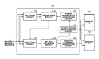
- FIG. 1 is a block diagram schematically illustrating a memory control circuit.
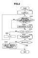
- FIG. 2 illustrates a control flow by an arbitration circuit.
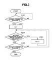
- FIG. 3 illustrates a control flow by a counter circuit.
- FIG. 4 illustrates a control flow by an arbitration circuit.
- FIG. 5 is a block diagram schematically illustrating a memory control circuit.
- FIG. 6 is a flowchart illustrating processing in which a reorder circuit determines where in an access storing circuit an externally provided access request is registered.
- FIG. 7 is a flowchart illustrating processing in which, in response to an instruction received from the reorder circuit, the access storing circuit changes the order of accesses.
- FIG. 8 illustrates an example of waveforms illustrating an operation of the memory control circuit.
- FIG. 9 illustrates an example of waveforms observed when a reorder function is disabled.
- FIG. 10 is a flowchart illustrating processing in which the reorder circuit determines where in the access storing circuit an externally provided access request to be reregistered.
- FIG. 1 is a block diagram schematically illustrating the configuration of the memory control circuit.
- the memory control circuit 100 accesses a plurality of memories 110 and 111 capable of shifting to a power saving mode (a power saving state).
- a power saving mode control circuit 101 which is connected to the memories 110 and 111 , brings these memories 110 and 111 into or out of the power saving mode (the power saving state).
- a power saving mode monitoring circuit 102 monitors whether the memories 110 and 111 (e.g. DRAM, DDR-SDRAM, DDR2-SDRAM, DDR3-SDRAM, DDR4-SDRAM) are placed in the power saving mode by the power saving mode control circuit 101 .
- An access storing circuit 103 retains a plurality of memory access commands (hereinafter referred to simply as “accesses”).
- a memory command generation circuit 104 which is connected with the memories 110 and 111 , retrieves an access registered at the top in the access storing circuit 103 , converts the access to a command for accessing the memory 110 or 111 , and issues the command.
- a decoding circuit 105 decodes an address to determine whether an externally provided access is to the memory 110 or to the memory 111 .
- an arbitration circuit 106 determines a bus master module (hereinafter referred to as a “bus master”) whose access is granted among a plurality of memory access requests.
- a selection circuit 107 selects the access determined by the arbitration circuit 106 , and registers the selected access in the access storing circuit 103 .
- FIG. 2 is a flowchart illustrating processing in which the arbitration circuit 106 illustrated in FIG. 1 determines which of the access requests from the bus masters is selected. In response to a transfer request made from a bus master, the arbitration circuit 106 starts an arbitration operation. First, in step S 201 , the arbitration circuit 106 clears an internal variable i and a list in which access requests to a memory that is not in the power saving mode are to be tallied.
- step S 202 the arbitration circuit 106 registers, in the list, the bus master numbers of the bus masters that have issued an access request to the memory that is not in the power saving mode, in sequence starting with a bus master 0 .
- the arbitration circuit 106 selects a bus master that is granted the access from the bus masters registered in the list.
- a known arbitration algorithm such as a fixed priority scheme and a round robin scheme, may be employed as the bus master selection method.
- step S 207 If a bus master registered in the list is selected (YES in step S 207 ), the process ends as it is. However, if no bus masters are registered in the list (NO in step S 207 ), the arbitration circuit 106 again selects a bus master that is granted the access from bus masters including those that are not on the list.
- the access request to the memory that is not placed in the power saving mode is preferentially selected. This causes the access request to the memory placed in the power saving mode to wait, allowing that memory in the power saving mode to remain in the power saving mode for a long time. Furthermore this causes the plurality of access requests to the memory packed, allowing that decreasing a number of changing state between power saving mode and normal mode, and decreasing power consumption and time for changing state.
- a transition to the power saving mode, and a return to the normal state from the power saving mode require more power than a refresh in the normal state.
- the power required for the state transitions will reduce power efficiency, contrary to the desired effect.
- the configuration illustrated in FIG. 1 allows a memory to remain in the power saving mode for a long time, so that reduction in power efficiency can be suppressed.
- FIG. 1 illustrates the memory control circuit including three bus masters and two memories. However, the present invention may be applied to any memory control circuits that include two or more memories, to accomplish more effective power saving.
- the list of the arbitration circuit 106 is stored in a storage unit (not illustrated) therein.
- the arbitration circuit 106 includes a counter (not illustrated) for each bus master to count the number of times other bus masters have been selected in spite of the presence of a transfer request made from the bus master. When the count value reaches a predetermined number of times, even the access request to the bus master being in the power saving mode is added to the list.
- FIG. 3 illustrates how the counter operates to count the number of times other bus masters have been selected after the issuance of a transfer request.
- the counter waits until a memory access (a transfer request) from a bus master is asserted (YES in step S 301 ), and then in step S 302 , clears a count value i in response to the assertion of the transfer request.
- step S 303 and S 304 the counter takes a count each time a transfer request from another bus master is accepted.
- step S 305 when the initial transfer request is accepted, the counter ends the counting. This counter is provided for each bus master.
- FIG. 4 is a flowchart illustrating the processing in the flowchart in FIG. 2 and an additional processing (step S 403 ).
- step S 403 the arbitration circuit 106 illustrated in FIG. 1 determines which of the access requests from the bus masters is selected using the value of the counter illustrated in FIG. 3 .
- the access request to the memory being in the power saving mode that has not been granted the predetermined number of times or more is handled in the same manner as the access to the memory that is not in the power saving mode.
- the arbitration circuit 106 includes a counter for each bus master, and counts the elapsed time since the initiation of a transfer request. When the count value reaches a predetermined period of time, even the access request to the bus master that is in the power saving mode is added to the list.
- a flowchart illustrating how the counter operates to count the elapsed time since the issuance of a transfer request is similar to that illustrated in FIG. 3 .
- the counter for counting the amount of time elapsed after the issuance of the transfer request is provided for each bus master.
- FIG. 4 is a flowchart illustrating processing in which the arbitration circuit 106 illustrated in FIG. 1 determines which of the access requests from the bus masters is selected using the value of the counter illustrated in FIG. 3 . According to the flow of processing illustrated in FIG. 4 , when a predetermined amount of time or longer has elapsed since the issuance of the transfer request, the access request to the memory being in the power saving mode is handled in the same manner as the access to the memory that is not in the power saving mode.
- the memory access to the memory that is not in the power saving mode are preferentially stored in the access storing circuit 103 .
- the arbitration circuit 106 stores the list of candidates for the bus master to be selected by the arbitration circuit 106 .
- the arbitration circuit 106 does not have to store such information in the form of a list, but may simply store identification information (ID) of bus masters.
- ID identification information
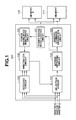
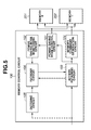
- FIG. 5 is a block diagram schematically illustrating the memory control circuit.
- the memory control circuit 100 controls accesses to memories 201 and 202 .
- a power saving mode control circuit 101 brings the memories 201 and 202 into or out of a power saving mode.
- a power saving mode monitoring circuit 102 monitors whether the memories 201 and 202 are placed in the power saving mode by the power saving mode control circuit 101 .
- An access storing circuit 103 retains a plurality of access requests to the memories 201 and 202 .
- a memory command generation circuit 104 retrieves an access registered at the top in the access storing circuit 103 , converts the access to a command for accessing the memory 201 or 202 , and issues the command.
- a decoding circuit 105 decodes an externally provided access to determine whether the access is to the memory 201 or to the memory 202 .
- a reorder circuit 106 determines where in the access storing circuit 103 the externally provided access is registered, according to the plurality of accesses retained by the access storing circuit 103 , the result of the decoding obtained by the decoding circuit 105 , and information obtained by the power saving mode monitoring circuit 102 .
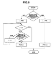
- FIG. 6 is a flowchart illustrating processing in which the reorder circuit 106 determines where in the access storing circuit 103 an externally provided access is registered.
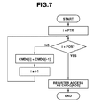
- FIG. 7 is a flowchart illustrating processing in which, in response to an instruction received from the reorder circuit 106 , the access storing circuit 103 changes the order of accesses.
- the access storing circuit 103 stores the number of accesses PTR.
- the access storing circuit 103 further stores an access array CMDQ.
- a character POS indicates where in the access array CMDQ the externally provided access is registered.
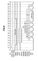
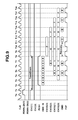
- FIG. 8 illustrates an example of waveforms illustrating the operation of the memory control circuit 100 .
- a clock CLK operates the memory control circuit 100 and the memories 201 and 202 .
- Trigger signals PDWN_EN[ 0 ] and PDWN_EN[ 1 ] provided from an external unit (not illustrated) are signals for placing the memories 201 and 202 in the power saving mode.
- the power saving mode control circuit 101 places the memory 201 in the power saving mode.
- the power saving mode control circuit 101 places the memory 202 in the power saving mode.
- Signals CKE[ 0 ] and CKE[ 1 ] are signals for placing the memories 201 and 202 in the power saving mode.
- the memory 201 is placed in the power saving mode.
- the signal CKE[ 1 ] goes to the ‘L’ level, the memory 202 is placed in the power saving mode.
- a trigger signal PUSH is a signal externally provided for registering an externally provided access in the access storing circuit 103 .
- the trigger signal PUSH is at an ‘H’ level, an externally provided access CMD_IN is registered in the access storing circuit 103 .
- Accesses CMDQ[ 0 ] to CMDQ[ 3 ] are registered in the access storing circuit 103 .
- the memory command generation circuit 104 retrieves the accesses CMDQ[ 0 ] to CMDQ[ 3 ] in sequence starting from the access CMDQ[ 0 ].
- An access CMD is generated by the memory command generation circuit 104 and transmitted to the memories 201 and 202 .
- a trigger signal POP is used for retrieving, by the memory command generation circuit 104 , an access located at the top in the access storing circuit 103 .
- the trigger signal POP goes to an ‘H’ level, the access storing circuit 103 shifts the access CMDQ by one.
- the power saving mode control circuit 101 puts the signal CKE[ 1 ] to the ‘L’ level.
- the memory 202 makes a transition to the power saving mode.
- accesses A to F are input to the access storing circuit 103 as the access CMD_IN.
- the accesses C and E are to the memory 202
- the other accesses A, B, D, and F are to the memory 201 .
- the access A is input to the access storing circuit 103 .
- the decoding circuit 105 calculates the fact that the access A is to the memory 201 , and informs the reorder circuit 106 of the fact.
- the reorder circuit 106 generates POS indicating where in the access storing circuit 103 the access A is registered, based on the processing illustrated in FIG. 6 .
- POS 0.
- the access storing circuit 103 registers the access A as the access CMDQ[ 0 ].
- the access B is input to the access storing circuit 103 .
- the decoding circuit 105 calculates the fact that the access B is to the memory 201 , and informs the reorder circuit 106 of the fact.
- the reorder circuit 106 generates POS indicating where in the access storing circuit 103 the access B is registered, based on the processing illustrated in FIG. 6 .
- POS 1.
- the access storing circuit 103 registers the access B as the access CMDQ[ 1 ].
- the access A is issued to the memory 201 , and the trigger signal POP goes to the ‘H’ level.
- the trigger signal PUSH goes to the ‘H’ level.
- the access C is input to the access storing circuit 103 .
- the decoding circuit 105 calculates the fact that the access C is to the memory 202 , and informs the reorder circuit 106 of the fact.
- the reorder circuit 106 generates POS indicating where in the access storing circuit 103 the access C is registered, based on the processing illustrated in FIG. 6 .
- POS 2.
- the access storing circuit 103 registers the access C as the access CMDQ[ 2 ].
- the trigger signal POP is at the ‘H’ level, causing the access storing circuit 103 to shift the access CMDQ by one to register the access B as the access CMDQ[ 0 ] and the access C as the access CMDQ[ 1 ].
- the access D is input to the access storing circuit 103 .
- the decoding circuit 105 calculates the fact that the access D is to the memory 201 , and informs the reorder circuit 106 of the fact.
- the reorder circuit 106 generates POS indicating where in the access storing circuit 103 the access D should be registered, based on the processing illustrated in FIG. 6 .
- the access B is issued to the memory 201 , and the trigger signal POP goes to the ‘H’ level.
- the trigger signal PUSH is at the ‘H’ level
- the access E is input to the access storing circuit 103 .
- the decoding circuit 105 calculates the fact that the access E is to the memory 202 , and informs the reorder circuit 106 of the fact.
- the reorder circuit 106 generates POS indicating where in the access storing circuit 103 the access E is registered, based on the processing illustrated in FIG. 6 .
- POS 3.
- the access storing circuit 103 registers the access C as the access CMDQ[ 3 ].
- the access storing circuit 103 shifts the access CMDQ by one to register the access E as the access CMDQ[ 2 ].
- the trigger signal PUSH is at the ‘H’ level, and thus the access F is input to the access storing circuit 103 .
- the decoding circuit 105 calculates the fact that the access F is to the memory 201 , and informs the reorder circuit 106 of the fact.
- the reorder circuit 106 generates POS indicating where in the access storing circuit 103 the access F is registered, based on the processing illustrated in FIG. 6 .
- the access C is at the top in the access storing circuit 103 , and the power saving mode control circuit 101 turns off the power saving mode of the memory 202 .
- the power saving mode control circuit 101 puts the signal CKE[ 1 ] to the ‘H’ level.
- the memory 202 detects that the signal CKE[ 1 ] is at the ‘H’ level, and goes out of the power saving mode.
- the memory command generation circuit 104 waits until the memory 202 returns from the power saving mode, and then issues the access C.
- the memories 201 and 202 require three cycles to return from the power saving mode.
- the access E is issued to the memory 202 .
- FIG. 9 illustrates waveforms observed when the reorder function is disabled.
- the memory 202 is placed in the power saving mode for six cycles.
- the time during which the memory 202 is placed in the power saving mode is extended to eleven cycles.
- an upper limit may be set for the number of times one access is overtaken by another access.
- the access storing circuit 103 includes a counter for each access, and counts the number of times the access has been overtaken by another access. When the count value has reached a predetermined number of times, the access storing circuit 103 informs the reorder circuit 106 of that fact. The reorder circuit 106 generates POS so that the access whose count value has reached the predetermined number of times will not be overtaken by other accesses.
- FIG. 10 illustrates an example of processing in which the reorder circuit 106 determines where in the access storing circuit 103 the access is registered at this time.
- the processing in FIG. 10 can set a limit so that each access that has been overtaken by other accesses a predetermined number of times will no longer be overtaken by other accesses.
- an upper limit may be set in term of time so that once a predetermined period of time has elapsed since one access is registered in the access storing circuit 103 , that access will not be overtaken by other accesses.
- the access storing circuit 103 includes a counter for each access, and counts the number of cycles that have elapsed since the registration of the access in the access storing circuit 103 . When the count value reaches a predetermined number of times, the access storing circuit 103 informs the reorder circuit 106 of that fact. The reorder circuit 106 generates POS so that the access whose count value has reached the predetermined number of times will not be overtaken by other accesses.
- the processing in which the reorder circuit 106 determines where in the access storing circuit 103 the access is registered at this time is the same as that illustrated in FIG. 10 in the second exemplary embodiment. In this way, a limit can be set so that each access that has been registered in the access storing circuit 103 for a predetermined period of time will no longer be overtaken by other accesses.
- accesses to a memory placed in a power saving mode are assigned a low priority when processed. This processing enables the memory to be placed in the power saving mode for a long time, so that the power consumption in the entire system can be reduced.
- an output interface may be provided which preferentially outputs, from a configuration that simply stores a plurality of access requests, a memory access request to a memory that is not in a power saving state.
Landscapes
- Engineering & Computer Science (AREA)
- Theoretical Computer Science (AREA)
- Physics & Mathematics (AREA)
- General Engineering & Computer Science (AREA)
- General Physics & Mathematics (AREA)
- Power Sources (AREA)
- Memory System (AREA)
Applications Claiming Priority (2)
| Application Number | Priority Date | Filing Date | Title |
|---|---|---|---|
| JP2010209418 | 2010-09-17 | ||
| JP2010-209418 | 2010-09-17 |
Publications (2)
| Publication Number | Publication Date |
|---|---|
| US20120072681A1 US20120072681A1 (en) | 2012-03-22 |
| US8856465B2 true US8856465B2 (en) | 2014-10-07 |
Family
ID=45818779
Family Applications (1)
| Application Number | Title | Priority Date | Filing Date |
|---|---|---|---|
| US13/225,294 Expired - Fee Related US8856465B2 (en) | 2010-09-17 | 2011-09-02 | Memory control apparatus and memory control method for controlling the priority of memory accesses |
Country Status (2)
| Country | Link |
|---|---|
| US (1) | US8856465B2 (ja) |
| JP (1) | JP5932261B2 (ja) |
Families Citing this family (3)
| Publication number | Priority date | Publication date | Assignee | Title |
|---|---|---|---|---|
| JP7159002B2 (ja) * | 2018-10-26 | 2022-10-24 | キヤノン株式会社 | 動作停止信号に従って動作停止状態となり、且つ、少なくとも動作停止信号が入力されていないことを条件に省電力モードに移行可能なデバイスを備える情報処理装置 |
| US10698846B2 (en) * | 2018-11-07 | 2020-06-30 | Realtek Semiconductor Corporation | DDR SDRAM physical layer interface circuit and DDR SDRAM control device |
| JP7292044B2 (ja) * | 2019-02-07 | 2023-06-16 | キヤノン株式会社 | 制御装置および制御方法 |
Citations (4)
| Publication number | Priority date | Publication date | Assignee | Title |
|---|---|---|---|---|
| JPH08153065A (ja) | 1994-11-30 | 1996-06-11 | Nec Corp | バス制御回路 |
| US5664089A (en) * | 1994-04-26 | 1997-09-02 | Unisys Corporation | Multiple power domain power loss detection and interface disable |
| US20090046523A1 (en) * | 2007-08-17 | 2009-02-19 | Fujitsu Limited | Semiconductor memory device and control method thereof |
| US20100005209A1 (en) * | 2004-06-24 | 2010-01-07 | Tetsuji Mochida | Arbitration device for arbitrating among a plurality of master devices, arbitration method, and video processing device including the arbitration device |
Family Cites Families (2)
| Publication number | Priority date | Publication date | Assignee | Title |
|---|---|---|---|---|
| US7581073B2 (en) * | 2006-08-09 | 2009-08-25 | International Business Machines Corporation | Systems and methods for providing distributed autonomous power management in a memory system |
| US9842068B2 (en) * | 2010-04-14 | 2017-12-12 | Qualcomm Incorporated | Methods of bus arbitration for low power memory access |
-
2011
- 2011-07-22 JP JP2011161055A patent/JP5932261B2/ja not_active Expired - Fee Related
- 2011-09-02 US US13/225,294 patent/US8856465B2/en not_active Expired - Fee Related
Patent Citations (4)
| Publication number | Priority date | Publication date | Assignee | Title |
|---|---|---|---|---|
| US5664089A (en) * | 1994-04-26 | 1997-09-02 | Unisys Corporation | Multiple power domain power loss detection and interface disable |
| JPH08153065A (ja) | 1994-11-30 | 1996-06-11 | Nec Corp | バス制御回路 |
| US20100005209A1 (en) * | 2004-06-24 | 2010-01-07 | Tetsuji Mochida | Arbitration device for arbitrating among a plurality of master devices, arbitration method, and video processing device including the arbitration device |
| US20090046523A1 (en) * | 2007-08-17 | 2009-02-19 | Fujitsu Limited | Semiconductor memory device and control method thereof |
Also Published As
| Publication number | Publication date |
|---|---|
| JP5932261B2 (ja) | 2016-06-08 |
| US20120072681A1 (en) | 2012-03-22 |
| JP2012084123A (ja) | 2012-04-26 |
Similar Documents
| Publication | Publication Date | Title |
|---|---|---|
| CN109564556B (zh) | 具有条纹和读取/写入事务管理的存储器控制器仲裁器 | |
| CN107924375B (zh) | 用于高速存储器接口的命令仲裁 | |
| CN110729006B (zh) | 存储器控制器中的刷新方案 | |
| JP4786209B2 (ja) | メモリアクセス装置 | |
| US8707002B2 (en) | Control apparatus | |
| US8169852B2 (en) | Memory control circuit, control method, and storage medium | |
| US7418535B2 (en) | Bus system and method of arbitrating the same | |
| JP2019522257A (ja) | 低電力メモリのスロットリング | |
| US20110082956A1 (en) | Information processing system and control method thereof | |
| KR20230017865A (ko) | Dram을 위한 리프레시 관리 | |
| JP2024512625A (ja) | アービトレーション中の書き込みバンクグループのマスク | |
| US8856465B2 (en) | Memory control apparatus and memory control method for controlling the priority of memory accesses | |
| US20050182908A1 (en) | Method and apparatus of interleaving memory bank in multi-layer bus system | |
| JP2001356961A (ja) | 調停装置 | |
| KR20230023014A (ko) | Dram 커맨드 스트리크 관리 | |
| US9189050B1 (en) | Method and apparatus for memory power reduction | |
| EP3270294B1 (en) | Command arbitration for high-speed memory interfaces | |
| KR20230004912A (ko) | 효율적인 메모리 버스 관리 | |
| JP2008059047A (ja) | 情報処理システム及びこの制御方法 | |
| JP4689965B2 (ja) | メモリ制御回路およびメモリ制御方法 | |
| US11687281B2 (en) | DRAM command streak efficiency management | |
| JP2006164099A (ja) | メモリ制御装置 | |
| JP2004070880A (ja) | メモリインターフェース回路 | |
| JP2002244919A (ja) | Dramインターフェース回路 |
Legal Events
| Date | Code | Title | Description |
|---|---|---|---|
| AS | Assignment |
Owner name: CANON KABUSHIKI KAISHA, JAPAN Free format text: ASSIGNMENT OF ASSIGNORS INTEREST;ASSIGNORS:FUJIWARA, MAKOTO;OCHIAI, WATARU;REEL/FRAME:027339/0418 Effective date: 20110822 |
|
| STCF | Information on status: patent grant |
Free format text: PATENTED CASE |
|
| MAFP | Maintenance fee payment |
Free format text: PAYMENT OF MAINTENANCE FEE, 4TH YEAR, LARGE ENTITY (ORIGINAL EVENT CODE: M1551) Year of fee payment: 4 |
|
| FEPP | Fee payment procedure |
Free format text: MAINTENANCE FEE REMINDER MAILED (ORIGINAL EVENT CODE: REM.); ENTITY STATUS OF PATENT OWNER: LARGE ENTITY |
|
| LAPS | Lapse for failure to pay maintenance fees |
Free format text: PATENT EXPIRED FOR FAILURE TO PAY MAINTENANCE FEES (ORIGINAL EVENT CODE: EXP.); ENTITY STATUS OF PATENT OWNER: LARGE ENTITY |
|
| STCH | Information on status: patent discontinuation |
Free format text: PATENT EXPIRED DUE TO NONPAYMENT OF MAINTENANCE FEES UNDER 37 CFR 1.362 |
|
| FP | Lapsed due to failure to pay maintenance fee |
Effective date: 20221007 |