US8841685B2 - Optoelectronic semiconductor chip - Google Patents
Optoelectronic semiconductor chip Download PDFInfo
- Publication number
- US8841685B2 US8841685B2 US13/056,589 US200913056589A US8841685B2 US 8841685 B2 US8841685 B2 US 8841685B2 US 200913056589 A US200913056589 A US 200913056589A US 8841685 B2 US8841685 B2 US 8841685B2
- Authority
- US
- United States
- Prior art keywords
- current spreading
- layer
- spreading layer
- semiconductor chip
- optoelectronic semiconductor
- Prior art date
- Legal status (The legal status is an assumption and is not a legal conclusion. Google has not performed a legal analysis and makes no representation as to the accuracy of the status listed.)
- Expired - Fee Related, expires
Links
Images


Classifications
-
- H01L33/387—
-
- H—ELECTRICITY
- H10—SEMICONDUCTOR DEVICES; ELECTRIC SOLID-STATE DEVICES NOT OTHERWISE PROVIDED FOR
- H10H—INORGANIC LIGHT-EMITTING SEMICONDUCTOR DEVICES HAVING POTENTIAL BARRIERS
- H10H20/00—Individual inorganic light-emitting semiconductor devices having potential barriers, e.g. light-emitting diodes [LED]
- H10H20/80—Constructional details
- H10H20/83—Electrodes
- H10H20/831—Electrodes characterised by their shape
- H10H20/8316—Multi-layer electrodes comprising at least one discontinuous layer
-
- H01L33/42—
-
- H—ELECTRICITY
- H10—SEMICONDUCTOR DEVICES; ELECTRIC SOLID-STATE DEVICES NOT OTHERWISE PROVIDED FOR
- H10H—INORGANIC LIGHT-EMITTING SEMICONDUCTOR DEVICES HAVING POTENTIAL BARRIERS
- H10H20/00—Individual inorganic light-emitting semiconductor devices having potential barriers, e.g. light-emitting diodes [LED]
- H10H20/80—Constructional details
- H10H20/83—Electrodes
- H10H20/832—Electrodes characterised by their material
- H10H20/833—Transparent materials
-
- H—ELECTRICITY
- H10—SEMICONDUCTOR DEVICES; ELECTRIC SOLID-STATE DEVICES NOT OTHERWISE PROVIDED FOR
- H10H—INORGANIC LIGHT-EMITTING SEMICONDUCTOR DEVICES HAVING POTENTIAL BARRIERS
- H10H20/00—Individual inorganic light-emitting semiconductor devices having potential barriers, e.g. light-emitting diodes [LED]
- H10H20/80—Constructional details
- H10H20/83—Electrodes
- H10H20/832—Electrodes characterised by their material
- H10H20/835—Reflective materials
-
- H—ELECTRICITY
- H01—ELECTRIC ELEMENTS
- H01L—SEMICONDUCTOR DEVICES NOT COVERED BY CLASS H10
- H01L2924/00—Indexing scheme for arrangements or methods for connecting or disconnecting semiconductor or solid-state bodies as covered by H01L24/00
-
- H—ELECTRICITY
- H01—ELECTRIC ELEMENTS
- H01L—SEMICONDUCTOR DEVICES NOT COVERED BY CLASS H10
- H01L2924/00—Indexing scheme for arrangements or methods for connecting or disconnecting semiconductor or solid-state bodies as covered by H01L24/00
- H01L2924/0001—Technical content checked by a classifier
- H01L2924/0002—Not covered by any one of groups H01L24/00, H01L24/00 and H01L2224/00
-
- H01L33/405—
Definitions
- the present invention is related to an optoelectronic semiconductor chip having an improved luminous efficiency.
- the luminous efficiency of radiation-emitting semiconductor chips is dependent on various factors. On the one hand, a relatively high internal quantum efficiency can be obtained by means of a large-area electrical contact-connection of the semiconductor chip. On the other hand, however, absorption losses can occur as a result of a large-area contact-connection, said absorption losses considerably restricting the coupling-out efficiency and hence the luminous efficiency of the semiconductor chip.
- One object of the present invention is to provide an optoelectronic semiconductor chip having an improved luminous efficiency.
- the opto-electronic semiconductor chip comprises a semiconductor layer sequence, which comprises an active zone for generating electromagnetic radiation, and also a structured current spreading layer, which contains a transparent conductive oxide and is arranged on a main area of the semiconductor layer sequence, wherein the current spreading layer covers at least 30% and at most 60% of the main area.
- the active zone comprises a pn junction for the purpose of generating radiation.
- said pn junction can be formed by means of a p-conducting semiconductor layer and an n-conducting semiconductor layer, which directly adjoin one another.
- the actual radiation-generating structure for instance in the form of a doped or undoped quantum structure, is formed between the p-conducting layer and the n-conducting layer.
- the quantum structure can be embodied as a single quantum well (SQW) structure or multiple quantum well (MQW) structure or else as a quantum wire or quantum dot structure.
- the semiconductor layer sequence contains Al n Ga m In 1-n-m N where 0 ⁇ n ⁇ 1, 0 ⁇ m ⁇ 1, and n+m ⁇ 1.
- a semiconductor chip based on nitride compound semiconductors is suitable, in particular, for generating radiation having an emission wavelength in the short-wave range of the visible spectrum.
- the transparent conductive oxide is preferably a metal oxide such as, for example, zinc oxide, tin oxide, cadmium oxide, titanium oxide, indium zinc oxide, indium oxide or indium tin oxide (ITO).
- binary metal-oxygen compounds such as, for example, ZnO, SnO 2 , or In 2 O 3
- ternary metal-oxygen compounds such as, for example, Zn 2 SnO 4 , CdSnO 3 , ZnSnO 3 , MgIn 2 O 4 , GaInO 3 , Zn 2 In 2 O 5 or In 4 Sn 3 O 12 or mixtures of different transparent conductive oxides.
- no stoichiometric composition is required.
- the transparent conductive oxide can also be p- or n-doped.
- the current spreading layer makes it possible to obtain sufficiently good current spreading and energization of the semiconductor chip.
- optical absorption losses caused by the current spreading layer can be reduced by comparison with a whole-area current spreading layer.
- the current spreading layer covers 40% to 50% of the main area. Firstly, the absorption losses are advantageously reduced in the case of such an area coverage; secondly, sufficiently good current spreading in the current spreading layer can be ensured in the case of such an area coverage.
- a smaller area coverage is advantageous, in particular, if the generated radiation has an emission wavelength of between 400 nm and 450 nm.
- the optical absorption caused by the current spreading layer constitutes a greater loss mechanism than the electrical losses on account of the smaller area coverage.
- the losses caused by the optical absorption are lower, such that the electrical losses are of greater consequence in the case of a smaller area coverage. Therefore, a larger area coverage is better suited in this case.
- the thickness of the current spreading layer can advantageously be between 10 nm and 60 nm. While the optical absorption losses can be reduced by reducing the thickness, in this case the transverse conductivity decreases at the same time. With a thickness of between 10 nm and 60 nm, gain and loss are in a suitable ratio to one another.
- the size, that is to say the length and/or width of interspaces of the structured current spreading layer, that is to say of regions which are not covered by the current spreading layer, is advantageously adapted to the transverse conductivity of the semiconductor material of the semiconductor layer sequence that adjoins the current spreading layer.
- the interspaces therefore advantageously have a size of between 1 ⁇ m and 6 ⁇ m.
- the interspaces are formed with a size in the range of between 3 ⁇ m and 4 ⁇ m.
- the current spreading layer can be structured in various ways. By way of example, irregular structures or regular structures such as grids are conceivable.
- the structure of the current spreading layer corresponds to a rectangular grid.
- the grid comprises, in particular, a plurality of parallel strips composed of transparent conductive oxide which extend in a first direction, and a plurality of parallel strips composed of transparent conductive oxide which extend in a second direction, wherein the first direction runs perpendicular to the second direction.
- the distance between the parallel strips extending in the first direction can differ from the distance between the parallel strips extending in the second direction.
- the crossing points of the strips correspond to grid points.
- Electrical contact is made with the current spreading layer preferably by means of at least one electrical contact web.
- Said contact web extends, in particular, perpendicularly to a plane in which the current spreading layer is arranged, and touches the current spreading layer at a contact location provided therefor.
- the contact web can have the form of a truncated cone, truncated pyramid or cylinder.
- a plurality of contact webs are distributed regularly over the area of the current spreading layer.
- the respective contact location is preferably situated at a grid point. In this case, however, a contact location need not be provided at every grid point.
- the contact web contains a metal having a high conductivity.
- a material having a high reflectance is preferably used for the contact web.
- One suitable material is Ag, for example.
- the current spreading layer is arranged between the semiconductor layer sequence and a mirror.
- the electrical contact web runs in an opening of the mirror. If the contact web has a high reflectance, as already mentioned, then overall a high reflectivity can be obtained by means of the combination of mirror and contact web. As a result, the radiation emitted by the active zone in the direction of the current spreading layer can be reflected without great optical losses in the direction of a coupling-out area.
- the coupling-out area is arranged, in particular, on a side of the active zone which lies opposite the current spreading layer. In addition, the optical losses are limited by virtue of the structured current spreading layer and the reduced area coverage associated therewith.
- the mirror comprises a dielectric layer.
- the dielectric layer has a lower refractive index than the semiconductor material of the semiconductor layer sequence.
- the dielectric layer is formed from a silicon oxide, a silicon nitride or glass, preferably a spin-on glass.
- the dielectric layer can also be embodied as a Bragg mirror, in which dielectric partial layers having different refractive indices are arranged alternately.
- the mirror in particular the dielectric layer, preferably adjoins the current spreading layer.
- the interspaces of the structured current spreading layer can be filled at least by a part of the mirror, in particular the dielectric layer. Furthermore, at least one part of the mirror or the dielectric layer can cover the current spreading layer.
- the opening in which the contact web extends is provided in the dielectric layer.
- the mirror advantageously comprises a continuous metal layer.
- the latter is arranged, in particular, on a side of the mirror which is remote from the current spreading layer.
- the dielectric layer is covered by the metal layer.
- the metal layer can be embodied at least in two-layered fashion.
- the metal layer can comprise a layer composed of platinum and/or titanium for adhesion promotion and a layer having a high reflectance, for example composed of silver.
- the semiconductor chip is a thin-film light-emitting diode chip.
- the semiconductor layer sequence is free of a growth substrate, that is to say that the growth substrate used for the growth of the semiconductor layer sequence is removed from the semiconductor layer sequence or at least greatly thinned.
- the latter can alternatively be arranged on a carrier substrate.
- the carrier substrate is situated on a rear side of the semiconductor chip lying opposite the coupling-out side.
- the current spreading layer is preferably arranged between the semiconductor layer sequence and the carrier substrate.
- the carrier substrate is electrically conductive and serves as a first electrical contact for the semiconductor chip.
- the current spreading layer is advantageously electrically connected to the carrier substrate by means of the electrical contact web, if appropriate via the metal layer of the mirror.
- a second electrical contact can be arranged on the coupling-out area.
- the semiconductor layer sequence is p-conducting on the side of the current spreading layer. Since the p-side typically has a poor conductivity, a current spreading layer having a high electrical conductivity is advantageous. Suitable dopant concentrations are in the range from 10 20 /cm 3 .
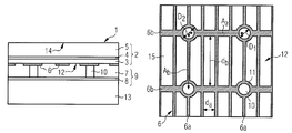
- FIG. 1 shows a schematic cross-sectional view of an optoelectronic semiconductor chip
- FIG. 2 shows a schematic view of a cross section along the current spreading layer of the semiconductor chip illustrated in FIG. 1 ,
- FIGS. 3A to 3D show the current density distribution over the main area with different area coverage
- FIG. 4 shows a graph illustrating the electrical losses at different current densities
- FIG. 5 shows a graph illustrating the extraction efficiency for different wavelengths
- FIGS. 6 to 8 show graphs illustrating the wall-plug efficiencies as a function of different current densities for different wavelengths.
- FIG. 1 shows an optoelectronic semiconductor chip 1 , comprising a semiconductor layer sequence 2 , having an active zone 4 for generating electromagnetic radiation.
- the active zone 4 is situated between a first semiconductor region 3 and a second semiconductor region 5 .
- the first semiconductor region 3 is p-conducting and the second semiconductor region 5 is n-conducting.
- the two semiconductor regions 3 , 5 contain GaN and the active zone 4 contains InGaN.
- the two semiconductor regions 3 , 5 and the active zone 4 can each comprise a plurality of semiconductor layers.
- the semiconductor layer sequence 2 is grown epitaxially, wherein the growth substrate (not illustrated) is stripped from the semiconductor layer sequence 2 , such that the semiconductor layer sequence 2 has a thickness of less than 10 ⁇ m.
- the semiconductor layer sequence 2 is alternatively arranged on a carrier substrate 13 .
- the carrier substrate 13 is preferably electrically conductive.
- Suitable substrates are Ge or Si substrates, for example.
- the carrier substrate 13 can be produced from Cu by means of electrolytic reinforcement of a preceding metal layer.
- a structured current spreading layer 6 is arranged on a main area 12 of the semiconductor layer sequence 2 .
- the current spreading layer 6 which contains a transparent conductive oxide, can be uniformly vapor-deposited or sputtered onto the main area 12 and subsequently structured in a suitable manner.
- the structuring can be effected lithographically, for example.
- the thickness of the current spreading layer 6 is advantageously between 10 nm and 60 nm. By reducing the thickness it is possible, on the one hand, for the optical absorption losses to be reduced, as a result of which, on the other hand, the transverse conductivity decreases. With a thickness of between 10 nm and 60 nm there is a good compromise between optical and electrical losses.
- a mirror 9 is arranged on the main area 12 , such that the radiation emitted in the direction of the main area 12 can be deflected in the direction of the coupling-out area 14 .
- the mirror 9 comprises a dielectric layer 7 , which is formed, in particular, from a material having a relatively low refractive index, for example from a spin-on glass having a refractive index of less than 1.4.
- the dielectric layer 7 can have a thickness in the range of 400 nm to 500 nm.
- the mirror 9 comprises a metal layer 8 adjoining the dielectric layer 7 .
- the metal layer 8 can be formed from an adhesion promotion layer composed of Pt and a reflection layer composed of Ag.
- the thickness of the metal layer 8 can be so thin that it has interruptions. A layer thickness of approximately 0.2 nm is sufficient.
- the structured current spreading layer 6 is embedded into the dielectric layer 7 .
- the dielectric layer 7 comprises openings in which contact webs 10 extend.
- the contact webs 10 run perpendicularly to a plane in which the current spreading layer 6 is arranged, and touch the latter at contact locations provided therefor.
- the contact webs 10 advantageously contain an electrically conductive material, such that the current spreading layer 6 can be energized by means of the contact webs 10 .
- the contact webs 10 can contain Ag, which additionally has a relatively high reflectance, such that the reflectivity of the mirror 9 is not significantly reduced at the contact webs 10 .
- the form of the contact webs 10 is preferably like a cylinder.
- the contact webs 10 can produce an electrical connection between the current spreading layer 6 and the, in particular, electrically conductive carrier substrate 13 .
- FIG. 2 shows the main area 12 on which the structured current spreading layer 6 is applied.
- the current spreading layer 6 has the form of a rectangular grid formed from parallel strips 6 a extending in a first direction and from parallel strips 6 b extending in a second direction.
- Contact locations 11 are provided at a plurality of grid points, that is to say at a plurality of crossing points of the strips 6 a and 6 b , at which contact locations the contact webs 10 are arranged.
- the contact locations 11 are produced from the same material as the strips 6 a and 6 b . They are circular in the same way as the cross sections of the contact webs 10 and are arranged concentrically with respect thereto.
- the contact locations 11 advantageously have a diameter D 2 of approximately 6 ⁇ m.
- the distances A b between the contact locations 11 in the first direction and the distances A a between the contact locations 11 in the second direction are preferably of the same magnitude and are approximately 20 ⁇ m.
- the diameter D 1 of the contact webs 10 is 4 ⁇ m.
- the strips 6 a are thinner than the strips 6 b and can be approximately 2 ⁇ m wide, while the strips 6 b are approximately 4 ⁇ m wide. Moreover, the strips 6 a are arranged more densely than the strips 6 b , that is to say the grid constants differ from one another in the first and second directions.
- the rectangular interspaces 15 delimited by the strips 6 a and 6 b , have a length d b of approximately 16 ⁇ m and a width d a of approximately 3 ⁇ m.
- FIGS. 3A to 3D show the current density distribution over the main area of a semiconductor chip as illustrated in FIG. 1 for different area coverages.
- the thickness of the current spreading layer 6 is 40 nm for all variants.
- the energization takes place with a nominal current density of 50 A/cm 2 in all variants.
- the area coverage is 100% in the variant illustrated in FIG. 3A , 50% in the variant illustrated in FIG. 3B , 40% in the variant illustrated in FIGS. 30 and 30% in the variant illustrated in FIG. 3D .
- the distances A b and A a are kept constant in the different variants in FIGS. 3B to 3D .
- the strip width is reduced.
- the interspaces 15 can be enlarged.
- the width d a (illustrated in FIG. 2 ) of the interspaces 15 can be approximately 4 ⁇ m in the variant illustrated in FIG. 3D , while it is 3 ⁇ m in the variant illustrated in FIG. 3B .
- Different current densities are represented by different gray levels, the current density in darker regions being higher than that in lighter regions.
- the graph in FIG. 4 reveals the electrical losses 1-L that occur in the current spreading layer.
- FIG. 5 shows, for different emission wavelengths ⁇ , the extraction efficiency E of a semiconductor chip with a mirror comprising a 500 nm thick SiO 2 layer and a 0.2 nm thick Pt/Ag layer, for the case where no current spreading layer is used (K 1 ) and for the case where a current spreading layer with 100% area coverage is used (K 2 ).
- the current spreading layer has a thickness of 30 nm.
- K 3 represents the absorption losses which are caused by the current spreading layer. This reveals that the absorption of the current spreading layer is greatly wavelength-dependent. Losses of approximately 20% occur in the shorter-wave range as a result of the current spreading layer, where they are approximately 5% in the longer-wave range.
- FIGS. 6 to 8 show the wall-plug efficiency WP, that is to say the electrical-to-optical efficiency, at emission wavelengths of 400 nm ( FIG. 6 ), 460 nm ( FIG. 7 ) and 540 nm ( FIG. 8 ).
- WP wall-plug efficiency
- the wall-plug efficiencies WP are specified at each wavelength for different current densities J and different area coverages of 100% (K 1 ), 50% (K 2 ), 40% (K 3 ) and 30% (K 4 ).
- the gain in extraction efficiency in the case of a structuring of the current spreading layer is not as great (approximately 6%) as in the shorter-wave range, because the transparency of the current spreading layer is higher and, consequently, electrical losses are of greater consequence.
- a current density of 200 A/cm 2 Up to a current density of 200 A/cm 2 , however, an area coverage of 40% to 50% is better than an area coverage of 100%.
Landscapes
- Led Devices (AREA)
Applications Claiming Priority (4)
| Application Number | Priority Date | Filing Date | Title |
|---|---|---|---|
| DE102008035110A DE102008035110A1 (de) | 2008-07-28 | 2008-07-28 | Optoelektronischer Halbleiterchip |
| DE102008035110.5 | 2008-07-28 | ||
| DE102008035110 | 2008-07-28 | ||
| PCT/DE2009/000917 WO2010012256A1 (de) | 2008-07-28 | 2009-06-29 | Optoelektronischer halbleiterchip |
Publications (2)
| Publication Number | Publication Date |
|---|---|
| US20110284893A1 US20110284893A1 (en) | 2011-11-24 |
| US8841685B2 true US8841685B2 (en) | 2014-09-23 |
Family
ID=41279336
Family Applications (1)
| Application Number | Title | Priority Date | Filing Date |
|---|---|---|---|
| US13/056,589 Expired - Fee Related US8841685B2 (en) | 2008-07-28 | 2009-06-29 | Optoelectronic semiconductor chip |
Country Status (8)
| Country | Link |
|---|---|
| US (1) | US8841685B2 (enExample) |
| EP (1) | EP2313935A1 (enExample) |
| JP (1) | JP5514819B2 (enExample) |
| KR (1) | KR101606604B1 (enExample) |
| CN (1) | CN102106008B (enExample) |
| DE (1) | DE102008035110A1 (enExample) |
| TW (1) | TWI415297B (enExample) |
| WO (1) | WO2010012256A1 (enExample) |
Families Citing this family (6)
| Publication number | Priority date | Publication date | Assignee | Title |
|---|---|---|---|---|
| WO2005094130A1 (ja) * | 2004-03-26 | 2005-10-06 | Matsushita Electric Works, Ltd. | 有機発光素子 |
| DE102008048648B4 (de) | 2008-09-24 | 2025-05-15 | OSRAM Opto Semiconductors Gesellschaft mit beschränkter Haftung | Optoelektronischer Halbleiterchip |
| DE102011017196A1 (de) | 2011-04-15 | 2012-10-18 | Osram Opto Semiconductors Gmbh | Polarisierte Strahlung emittierender Halbleiterchip |
| DE102015109786A1 (de) | 2015-06-18 | 2016-12-22 | Osram Opto Semiconductors Gmbh | Verfahren zur Herstellung eines optoelektronischen Halbleiterbauelements sowie optoelektronisches Halbleiterbauelement |
| CN105609596A (zh) * | 2015-09-11 | 2016-05-25 | 映瑞光电科技(上海)有限公司 | 具有电流阻挡结构的led垂直芯片及其制备方法 |
| DE102019103638A1 (de) | 2019-02-13 | 2020-08-13 | OSRAM Opto Semiconductors Gesellschaft mit beschränkter Haftung | Optoelektronisches halbleiterbauelement mit abschnitten einer leitfähigen schicht und verfahren zur herstellung eines optoelektronischen halbleiterbauelements |
Citations (23)
| Publication number | Priority date | Publication date | Assignee | Title |
|---|---|---|---|---|
| JPH11168239A (ja) | 1997-12-05 | 1999-06-22 | Matsushita Electric Ind Co Ltd | 窒化ガリウム系化合物半導体発光素子 |
| DE10017758A1 (de) | 1999-06-08 | 2000-12-21 | Agilent Technologies Inc | Verfahren zum Bilden von transparenten Kontakten an einer p-Typ-GaN-Schicht |
| US20020130327A1 (en) | 2001-03-19 | 2002-09-19 | Bor-Jen Wu | Light emitting diodes with spreading and improving light emitting area |
| US20020195606A1 (en) | 2001-01-16 | 2002-12-26 | Edmond John Adam | Group III nitride LED with undoped cladding layer and multiple quantum well |
| US20030010994A1 (en) * | 2000-07-26 | 2003-01-16 | Axt, Inc. | Window for GaN LED |
| DE10147886A1 (de) | 2001-09-28 | 2003-04-24 | Osram Opto Semiconductors Gmbh | Lumineszenzdiode und Herstellungsverfahren |
| US20030111667A1 (en) | 2001-12-13 | 2003-06-19 | Schubert E. Fred | Light-emitting diode with planar omni-directional reflector |
| US20030141506A1 (en) | 2002-01-28 | 2003-07-31 | Masahiko Sano | Nitride semiconductor element with a supporting substrate and a method for producing a nitride semiconductor element |
| US20040262620A1 (en) | 2002-12-31 | 2004-12-30 | Osram Opto Semiconductors Gmbh | Light emitting diode chip with radiation-transmissive electrical current expansion layer |
| US20050087884A1 (en) * | 2003-10-24 | 2005-04-28 | Stokes Edward B. | Flip-chip light emitting diode |
| US20050093002A1 (en) | 2003-10-30 | 2005-05-05 | United Epitaxy Company, Ltd. | Light emitting diode device and manufacturing method |
| JP2005123501A (ja) | 2003-10-20 | 2005-05-12 | Toyoda Gosei Co Ltd | 半導体発光素子 |
| DE102004029216A1 (de) | 2004-01-19 | 2005-08-11 | Samsung Electro-Mechanics Co., Ltd., Suwon | Flip-Chip-Nitrid-Halbleiter-Leuchtdiode |
| US20050253163A1 (en) | 2004-04-30 | 2005-11-17 | Osram Opto Semiconductors Gmbh | Optoelectronic component having a plurality of current expansion layers and method for producing it |
| JP2006310893A (ja) | 2002-10-03 | 2006-11-09 | Nichia Chem Ind Ltd | 発光ダイオード |
| JP2007207869A (ja) | 2006-01-31 | 2007-08-16 | Rohm Co Ltd | 窒化物半導体発光素子 |
| US20070194325A1 (en) | 2006-02-23 | 2007-08-23 | Ying-Che Sung | Light emitting diode by use of metal diffusion bonding technology and method of producing light emitting diode |
| JP2007281037A (ja) | 2006-04-03 | 2007-10-25 | Dowa Holdings Co Ltd | 半導体発光素子及びその製造方法 |
| DE102006034847A1 (de) | 2006-04-27 | 2007-10-31 | Osram Opto Semiconductors Gmbh | Optoelektronischer Halbleiterchip |
| US20070278508A1 (en) | 2004-01-26 | 2007-12-06 | Johannes Baur | Thin Film Led Comprising a Current-Dispersing Structure |
| US20080142824A1 (en) | 2006-12-18 | 2008-06-19 | Shih-Peng Chen | Electroluminescent device and fabrication method thereof |
| US20080315220A1 (en) | 2007-06-25 | 2008-12-25 | Dicon Fiberoptics, Inc. | High Light Efficiency Solid-State Light Emitting Structure And Methods To Manufacturing The Same |
| DE102008035900A1 (de) | 2008-04-30 | 2009-11-05 | Osram Opto Semiconductors Gmbh | Leuchtdiodenchip |
Family Cites Families (1)
| Publication number | Priority date | Publication date | Assignee | Title |
|---|---|---|---|---|
| JP2009260316A (ja) * | 2008-03-26 | 2009-11-05 | Panasonic Electric Works Co Ltd | 半導体発光素子およびそれを用いる照明装置 |
-
2008
- 2008-07-28 DE DE102008035110A patent/DE102008035110A1/de not_active Withdrawn
-
2009
- 2009-06-29 US US13/056,589 patent/US8841685B2/en not_active Expired - Fee Related
- 2009-06-29 JP JP2011520319A patent/JP5514819B2/ja not_active Expired - Fee Related
- 2009-06-29 EP EP09775928A patent/EP2313935A1/de not_active Withdrawn
- 2009-06-29 WO PCT/DE2009/000917 patent/WO2010012256A1/de not_active Ceased
- 2009-06-29 KR KR1020117004570A patent/KR101606604B1/ko not_active Expired - Fee Related
- 2009-06-29 CN CN200980129527.1A patent/CN102106008B/zh not_active Expired - Fee Related
- 2009-07-24 TW TW098124990A patent/TWI415297B/zh not_active IP Right Cessation
Patent Citations (31)
| Publication number | Priority date | Publication date | Assignee | Title |
|---|---|---|---|---|
| JPH11168239A (ja) | 1997-12-05 | 1999-06-22 | Matsushita Electric Ind Co Ltd | 窒化ガリウム系化合物半導体発光素子 |
| DE10017758A1 (de) | 1999-06-08 | 2000-12-21 | Agilent Technologies Inc | Verfahren zum Bilden von transparenten Kontakten an einer p-Typ-GaN-Schicht |
| TW471185B (en) | 1999-06-08 | 2002-01-01 | Lumileds Lighting Llc | Method of forming transparent contacts to a p-type GaN layer |
| US20030010994A1 (en) * | 2000-07-26 | 2003-01-16 | Axt, Inc. | Window for GaN LED |
| US20020195606A1 (en) | 2001-01-16 | 2002-12-26 | Edmond John Adam | Group III nitride LED with undoped cladding layer and multiple quantum well |
| US20020130327A1 (en) | 2001-03-19 | 2002-09-19 | Bor-Jen Wu | Light emitting diodes with spreading and improving light emitting area |
| DE10147886A1 (de) | 2001-09-28 | 2003-04-24 | Osram Opto Semiconductors Gmbh | Lumineszenzdiode und Herstellungsverfahren |
| US20030111667A1 (en) | 2001-12-13 | 2003-06-19 | Schubert E. Fred | Light-emitting diode with planar omni-directional reflector |
| WO2003052838A2 (en) | 2001-12-13 | 2003-06-26 | Rensselaer Polytechnic Institute | Light-emitting diode with planar omni-directional reflector |
| JP2005513787A (ja) | 2001-12-13 | 2005-05-12 | レンゼラー ポリテクニック インスティテュート | 平面全方位リフレクタを有する発光ダイオード |
| US20030141506A1 (en) | 2002-01-28 | 2003-07-31 | Masahiko Sano | Nitride semiconductor element with a supporting substrate and a method for producing a nitride semiconductor element |
| US20050035364A1 (en) | 2002-01-28 | 2005-02-17 | Masahiko Sano | Opposed terminal structure having a nitride semiconductor element |
| JP2006310893A (ja) | 2002-10-03 | 2006-11-09 | Nichia Chem Ind Ltd | 発光ダイオード |
| US20040262620A1 (en) | 2002-12-31 | 2004-12-30 | Osram Opto Semiconductors Gmbh | Light emitting diode chip with radiation-transmissive electrical current expansion layer |
| JP2005123501A (ja) | 2003-10-20 | 2005-05-12 | Toyoda Gosei Co Ltd | 半導体発光素子 |
| US20050087884A1 (en) * | 2003-10-24 | 2005-04-28 | Stokes Edward B. | Flip-chip light emitting diode |
| US20050093002A1 (en) | 2003-10-30 | 2005-05-05 | United Epitaxy Company, Ltd. | Light emitting diode device and manufacturing method |
| DE102004029216A1 (de) | 2004-01-19 | 2005-08-11 | Samsung Electro-Mechanics Co., Ltd., Suwon | Flip-Chip-Nitrid-Halbleiter-Leuchtdiode |
| US7057212B2 (en) | 2004-01-19 | 2006-06-06 | Samsung Electro-Mechanics Co., Ltd. | Flip chip nitride semiconductor light emitting diode |
| US20070278508A1 (en) | 2004-01-26 | 2007-12-06 | Johannes Baur | Thin Film Led Comprising a Current-Dispersing Structure |
| US20050253163A1 (en) | 2004-04-30 | 2005-11-17 | Osram Opto Semiconductors Gmbh | Optoelectronic component having a plurality of current expansion layers and method for producing it |
| JP2007207869A (ja) | 2006-01-31 | 2007-08-16 | Rohm Co Ltd | 窒化物半導体発光素子 |
| US20070194325A1 (en) | 2006-02-23 | 2007-08-23 | Ying-Che Sung | Light emitting diode by use of metal diffusion bonding technology and method of producing light emitting diode |
| JP2007281037A (ja) | 2006-04-03 | 2007-10-25 | Dowa Holdings Co Ltd | 半導体発光素子及びその製造方法 |
| DE102006034847A1 (de) | 2006-04-27 | 2007-10-31 | Osram Opto Semiconductors Gmbh | Optoelektronischer Halbleiterchip |
| US20100019268A1 (en) | 2006-04-27 | 2010-01-28 | Osram Opto Semiconductors Gmbh | Optoelectronic Semiconductor Chip |
| US20080142824A1 (en) | 2006-12-18 | 2008-06-19 | Shih-Peng Chen | Electroluminescent device and fabrication method thereof |
| TW200828642A (en) | 2006-12-18 | 2008-07-01 | Delta Electronics Inc | Electroluminescent device, and fabrication method thereof |
| US20080315220A1 (en) | 2007-06-25 | 2008-12-25 | Dicon Fiberoptics, Inc. | High Light Efficiency Solid-State Light Emitting Structure And Methods To Manufacturing The Same |
| DE102008035900A1 (de) | 2008-04-30 | 2009-11-05 | Osram Opto Semiconductors Gmbh | Leuchtdiodenchip |
| WO2009132641A1 (de) | 2008-04-30 | 2009-11-05 | Osram Opto Semiconductors Gmbh | Leuchtdiodenchip |
Non-Patent Citations (2)
| Title |
|---|
| J. K. Kim et al., "GaInN light-emitting diodes with RuO2/SiO2/Ag omni-directional reflector", Applied Physics Letters, vol. 84, No. 22, pp. 4508-4510, May 31, 2004. |
| J.K. Kim et al., "Enhanced light-extraction in GaInN near-ultraviolet light-emitting diode with Al-based omnidirectioal reflector having NiZn/AG microcontacts", Applied Physics Letters, vol. 89, No. 141123, 2006. |
Also Published As
| Publication number | Publication date |
|---|---|
| CN102106008B (zh) | 2014-12-24 |
| WO2010012256A1 (de) | 2010-02-04 |
| KR20110044264A (ko) | 2011-04-28 |
| KR101606604B1 (ko) | 2016-03-25 |
| DE102008035110A1 (de) | 2010-02-11 |
| EP2313935A1 (de) | 2011-04-27 |
| TW201013992A (en) | 2010-04-01 |
| TWI415297B (zh) | 2013-11-11 |
| CN102106008A (zh) | 2011-06-22 |
| JP2011529277A (ja) | 2011-12-01 |
| US20110284893A1 (en) | 2011-11-24 |
| JP5514819B2 (ja) | 2014-06-04 |
Similar Documents
| Publication | Publication Date | Title |
|---|---|---|
| US8067783B2 (en) | Radiation-emitting chip comprising at least one semiconductor body | |
| US8581280B2 (en) | Optoelectronic semiconductor chip | |
| KR100631840B1 (ko) | 플립칩용 질화물 반도체 발광소자 | |
| CN101681958B (zh) | 光电子半导体本体及其制造方法 | |
| US9117973B2 (en) | Semiconductor light emitting element | |
| US20090309120A1 (en) | LED Semiconductor Element, and Use Thereof | |
| US10446717B2 (en) | Optoelectronic semiconductor chip | |
| US20120098009A1 (en) | Semiconductor light emitting device and manufacturing method thereof | |
| KR101860973B1 (ko) | 광전 반도체 칩 | |
| JP6924836B2 (ja) | 光電子半導体チップ | |
| KR101111750B1 (ko) | 반도체 발광 소자 | |
| US8841685B2 (en) | Optoelectronic semiconductor chip | |
| US8115219B2 (en) | LED semiconductor body and use of an LED semiconductor body | |
| JP5165254B2 (ja) | フリップチップ型の発光素子 | |
| KR101259482B1 (ko) | 고효율 발광다이오드 | |
| US20110204322A1 (en) | Optoelectronic Semiconductor Body and Method for Producing an Optoelectronic Semiconductor Body | |
| KR20110086096A (ko) | 광전 반도체 소자 | |
| KR101205437B1 (ko) | 반도체 발광 소자 | |
| US20250022983A1 (en) | Current injection structures for light-emitting diode chips | |
| US10644201B2 (en) | Optoelectronic semiconductor chip | |
| KR100706949B1 (ko) | 고휘도 질화물계 반도체 발광소자 | |
| KR100650189B1 (ko) | 고휘도 질화물계 반도체 발광소자 |
Legal Events
| Date | Code | Title | Description |
|---|---|---|---|
| AS | Assignment |
Owner name: OSRAM OPTO SEMICONDUCTORS GMBH, GERMANY Free format text: ASSIGNMENT OF ASSIGNORS INTEREST;ASSIGNORS:HOEPPEL, LUTZ;SABATHIL, MATTHIAS;SIGNING DATES FROM 20110211 TO 20110215;REEL/FRAME:026169/0372 |
|
| FEPP | Fee payment procedure |
Free format text: PAYOR NUMBER ASSIGNED (ORIGINAL EVENT CODE: ASPN); ENTITY STATUS OF PATENT OWNER: LARGE ENTITY |
|
| STCF | Information on status: patent grant |
Free format text: PATENTED CASE |
|
| MAFP | Maintenance fee payment |
Free format text: PAYMENT OF MAINTENANCE FEE, 4TH YEAR, LARGE ENTITY (ORIGINAL EVENT CODE: M1551) Year of fee payment: 4 |
|
| FEPP | Fee payment procedure |
Free format text: MAINTENANCE FEE REMINDER MAILED (ORIGINAL EVENT CODE: REM.); ENTITY STATUS OF PATENT OWNER: LARGE ENTITY |
|
| LAPS | Lapse for failure to pay maintenance fees |
Free format text: PATENT EXPIRED FOR FAILURE TO PAY MAINTENANCE FEES (ORIGINAL EVENT CODE: EXP.); ENTITY STATUS OF PATENT OWNER: LARGE ENTITY |
|
| STCH | Information on status: patent discontinuation |
Free format text: PATENT EXPIRED DUE TO NONPAYMENT OF MAINTENANCE FEES UNDER 37 CFR 1.362 |
|
| FP | Lapsed due to failure to pay maintenance fee |
Effective date: 20220923 |