US8766526B2 - Light-emitting device package providing improved luminous efficacy and uniform distribution - Google Patents
Light-emitting device package providing improved luminous efficacy and uniform distribution Download PDFInfo
- Publication number
- US8766526B2 US8766526B2 US13/169,466 US201113169466A US8766526B2 US 8766526 B2 US8766526 B2 US 8766526B2 US 201113169466 A US201113169466 A US 201113169466A US 8766526 B2 US8766526 B2 US 8766526B2
- Authority
- US
- United States
- Prior art keywords
- layer
- light
- emitting device
- resin
- device package
- Prior art date
- Legal status (The legal status is an assumption and is not a legal conclusion. Google has not performed a legal analysis and makes no representation as to the accuracy of the status listed.)
- Active, expires
Links
Images


Classifications
-
- G—PHYSICS
- G02—OPTICS
- G02B—OPTICAL ELEMENTS, SYSTEMS OR APPARATUS
- G02B6/00—Light guides; Structural details of arrangements comprising light guides and other optical elements, e.g. couplings
- G02B6/0001—Light guides; Structural details of arrangements comprising light guides and other optical elements, e.g. couplings specially adapted for lighting devices or systems
- G02B6/0011—Light guides; Structural details of arrangements comprising light guides and other optical elements, e.g. couplings specially adapted for lighting devices or systems the light guides being planar or of plate-like form
- G02B6/0013—Means for improving the coupling-in of light from the light source into the light guide
- G02B6/0023—Means for improving the coupling-in of light from the light source into the light guide provided by one optical element, or plurality thereof, placed between the light guide and the light source, or around the light source
- G02B6/0025—Diffusing sheet or layer; Prismatic sheet or layer
-
- G—PHYSICS
- G02—OPTICS
- G02B—OPTICAL ELEMENTS, SYSTEMS OR APPARATUS
- G02B27/00—Optical systems or apparatus not provided for by any of the groups G02B1/00 - G02B26/00, G02B30/00
- G02B27/09—Beam shaping, e.g. changing the cross-sectional area, not otherwise provided for
- G02B27/0938—Using specific optical elements
- G02B27/095—Refractive optical elements
- G02B27/0972—Prisms
-
- H01L33/50—
-
- H01L33/52—
-
- H—ELECTRICITY
- H10—SEMICONDUCTOR DEVICES; ELECTRIC SOLID-STATE DEVICES NOT OTHERWISE PROVIDED FOR
- H10H—INORGANIC LIGHT-EMITTING SEMICONDUCTOR DEVICES HAVING POTENTIAL BARRIERS
- H10H20/00—Individual inorganic light-emitting semiconductor devices having potential barriers, e.g. light-emitting diodes [LED]
- H10H20/80—Constructional details
- H10H20/85—Packages
- H10H20/851—Wavelength conversion means
-
- H—ELECTRICITY
- H10—SEMICONDUCTOR DEVICES; ELECTRIC SOLID-STATE DEVICES NOT OTHERWISE PROVIDED FOR
- H10H—INORGANIC LIGHT-EMITTING SEMICONDUCTOR DEVICES HAVING POTENTIAL BARRIERS
- H10H20/00—Individual inorganic light-emitting semiconductor devices having potential barriers, e.g. light-emitting diodes [LED]
- H10H20/80—Constructional details
- H10H20/85—Packages
- H10H20/852—Encapsulations
-
- H—ELECTRICITY
- H10—SEMICONDUCTOR DEVICES; ELECTRIC SOLID-STATE DEVICES NOT OTHERWISE PROVIDED FOR
- H10H—INORGANIC LIGHT-EMITTING SEMICONDUCTOR DEVICES HAVING POTENTIAL BARRIERS
- H10H20/00—Individual inorganic light-emitting semiconductor devices having potential barriers, e.g. light-emitting diodes [LED]
- H10H20/80—Constructional details
- H10H20/85—Packages
- H10H20/855—Optical field-shaping means, e.g. lenses
Definitions
- a light-emitting diode is a device which converts electric signals into light using characteristics of compound semiconductors. LEDs are now being applied to devices such as home appliances, remote controls, electronic signboards, displays, a variety of automatic appliances and the like and their application range continues to expand.
- a miniaturized LED is fabricated as a surface mount device such that it can be directly mounted to a printed circuit board (PCB). Accordingly, an LED lamp used as a display device is also developed in a surface mount device-type. Such a surface mount device may substitute for a conventional lamp and is used as lighting displays, character displays, image displays and the like, rendering various colors.
- embodiments disclosed herein provide a light-emitting device package providing improved luminous efficacy and uniform distribution of light emitted by a light emitting device in the package.
- the plural linear prisms may form prism patterns arranged in parallel to one another.
- the optical sheet may further include a third layer formed at the bottom of the first layer.
- the optical sheet may comprise at least one selected from polyethylene terephthalate, polycarbonate, polyethylene, polystyrene, polyester resin, polyether resin, epoxy resin, urethane resin, spiroacetyl resin, polybutadiene resin, polythiolpolyene resin, or the like.
- the third layer may include phosphors.
- the second layer may include a first phosphor
- the third layer may include a second phosphor
- the first and second layers may emit different wavelengths of light.
- a light-emitting device package including; a body having a cavity formed therein, a light source mounted in the cavity, a resin layer which fills the cavity and is transmissive, and at least one optical sheet provided on the resin layer: wherein the optical sheet includes a first layer, a second layer which is provided on the first layer and has a plurality of linear prisms; wherein the first layer includes a first phosphor while the second layer includes a second phosphor; and wherein the first and second phosphors emit different wavelengths of light.
- the optical sheet may further include a third layer provided under the first layer and arranged between the first layer and the resin layer.
- the third layer may include phosphors.
- the second layer may include a first phosphor while the third layer may include a second phosphor, and the first and second phosphors may emit different wavelengths of light.
- the optical sheet may comprise a first optical sheet and a second optical sheet provided on the first optical sheet, wherein the first optical sheet has a first prism part arranged in a first direction and the second optical has a second prism part arranged in a second direction, and wherein the first and second directions form a first angle.
- the first angle may be a right angle.
- FIG. 1A is a cross-sectional view illustrating a configuration of a light-emitting device package according to one embodiment
- FIG. 1B is a cross-sectional view illustrating a configuration of a light-emitting device package according to another embodiment
- FIG. 2 is a perspective view illustrating a configuration of an optical sheet according to one embodiment
- FIG. 4 is a perspective view illustrating a configuration of an optical sheet according to one embodiment
- FIG. 7 is a perspective view illustrating a configuration of an optical sheet according to one embodiment
- FIG. 8 is a perspective view illustrating a configuration of an optical sheet according to one embodiment
- FIG. 9 is a perspective view illustrating a configuration of an optical sheet according to one embodiment.
- FIG. 11 is a perspective view illustrating a configuration of an optical sheet according to one embodiment
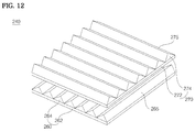
- FIG. 12 is an exploded perspective view illustrating a configuration of an optical sheet according to one embodiment
- FIG. 13 is a cross-sectional view illustrating a configuration of a light-emitting device package according to one embodiment
- FIG. 14 is a perspective view illustrating a configuration of an optical sheet according to one embodiment
- FIG. 15 is a perspective view illustrating a configuration of an optical sheet according to one embodiment
- FIG. 17 is a perspective view illustrating a configuration of an optical sheet according to one embodiment
- FIG. 18 is an exploded perspective view illustrating a configuration of an optical sheet according to one embodiment
- FIG. 19 is a conceptual view illustrating a process of preparing an optical sheet according to one embodiment
- FIG. 21 is a cross-sectional view illustrating a light-emitting device package according to one embodiment
- FIG. 25 is a perspective view illustrating a lighting instrument equipped with a light-emitting device package according to one embodiment
- FIG. 27 is an exploded perspective view illustrating a backlight unit equipped with a light-emitting device package according to one embodiment.
- FIG. 28 is an exploded perspective view illustrating a backlight unit equipped with a light-emitting device package according to one embodiment.
- a light-emitting device package 100 comprises: a body 110 having a cavity 112 formed therein; a light source 130 mounted to the bottom of the body 110 ; a resin layer 120 which fills the cavity 112 and is transmissive; and an optical sheet 140 provided on the resin layer 120 , wherein the optical sheet 140 has a first layer 142 , a second layer 144 which is provided on the first layer 142 and includes a plurality of linear prisms 145 , wherein the first layer 142 has a first refractive index and the resin layer 120 has a second refractive index, and wherein the first refractive index is equal to or greater than the second refractive index.
- the body 110 may be formed using at least one selected from polyphthalamide (PPA) as a resin material, silicon (Si), aluminum (Al), aluminum nitride (AlN), photosensitive glass (PSG), polyaminde 9T (PA9T), syndiotactic polystyrene (SPS), metal materials, sapphire (Al 2 O 3 ), beryllium oxide (BeO), a printed circuit board (PCB), or the like.
- PPA polyphthalamide
- the body 110 may be formed by injection molding, etching, etc., without being particularly limited thereto.
- the inner surface of the body 110 may be provided with an inclined surface.
- the reflective angle of light emitted from the light source 130 may be varied, depending on the angle of the inclined surface. Accordingly, the orientation angle of light discharged to the outside can be controlled.
- the cavity 112 provided in the body 110 may have various shapes including, but being not limited to, a circular shape, a rectangular shape, a polygonal shape, an oval shape and a shape with curved corners.
- the body 110 may have an electrode (not shown).
- the electrode (not shown) may be electrically connected to the light source 130 to supply power.
- the electrode may comprise at least one selected from titanium (Ti), copper (Cu), nickel (Ni), gold (Au), chromium (Cr), tantalum (Ta), platinum (Pt), tin (Sn), silver (Ag), phosphorous (P), aluminum (Al), indium (In), palladium (Pd), cobalt (Co), silicon (Si), germanium (Ge), hafnium (Hf), ruthenium (Ru), iron (Fe), or alloys thereof.
- the electrode (not shown) may be formed in a single layer or multi-layer structure, without being particularly limited thereto.
- the cavity 112 may include the resin layer 120 having light transmitting property. More particularly, the cavity 112 may be filled with the resin layer 120 having light transmitting property to protect the light source 130 from impurities or moisture.
- the resin layer 120 may be composed of silicone, epoxy or other resin materials and formed by filling the cavity 112 with such a resin material and UV or heat curing the same.
- the light-emitting device package 110 may be a wafer level package, as shown in FIG. 1B .
- the body 110 may be made of an electrically insulating material, for example, resin, ceramic, a silicon wafer, etc.
- the body 110 made of a silicon wafer is illustrated in one embodiment.
- a recess may be formed in a concave shape by selectively removing a top surface of the body 110 . Within the recess, the light emitting device 130 is located and the resin layer 120 may be formed.
- the body 110 may be provided with an optical sheet 140 and the optical sheet 140 may have a first layer 142 and a second layer 144 wherein the second layer 144 may have a plurality of linear prisms 145 formed thereon.
- the refractive index of the resin layer 120 is greater than that of the first layer 142 , total reflection may occur at a boundary between the resin layer 120 and the first layer 142 . Further, since light may be confined (entrapped) in the cavity 112 , light extraction efficiency of the light-emitting device package 100 may be reduced.
- the first layer 142 may be provided with a second layer 144 including a plurality of linear prisms 145 to refract light.
- the second layer 144 may be formed using acrylic resin, without being particularly limited thereto.
- acrylic resin for example, as described above, at least one selected from polyethylene terephthalate, polycarbonate, polyethylene, polystyrene, polyester resin, polyether resin, epoxy resin, urethane resin, spiroacetyl resin, polybutadiene resin, polythiolpolyene resin, or the like, may be used.
- the second layer 142 may be composed of the same material as the first layer 142 and integrated with the same, without being particularly limited thereto.
- the third layer 146 may prevent the optical sheet 140 from being modified by heat generated from the light source 130 and have excellent restoration, thus enabling the optical sheet 140 to return to an original shape thereof at room temperature, even when the optical sheet 140 is modified at high temperature.
- the third layer 146 may protect the optical sheet 140 from being scratched due to external impact or other physical force.
- the first optical sheet 160 may have a first layer 162 and a second layer 164 or a third layer (not shown) while the second optical sheet 170 may have a first layer 172 and a second layer 174 or a third layer (not shown), without being particularly limited thereto.
- the first optical sheet 160 and second optical sheet 170 may be secured to each other, using an adhesive, without being particularly limited thereto.
- a first linear prism part 165 provided on the second layer 164 of the first optical sheet 160 may extend in a first direction, while a second linear prism part 175 provided on the second layer 174 of the second optical sheet 170 may extend in a second direction forming a first angle relative to the first direction.
- the first angle may be a right angle, without being particularly limited thereto.
- the body 210 , cavity 212 , resin layer 220 and light source 230 are substantially the same as described above and, therefore, a detailed explanation thereof is omitted.
- the first or second layer 242 or 244 may have the phosphor 250 .
- the phosphor 250 may be any one selected from a blue light emitting phosphor, blue-green light emitting phosphor, green light emitting phosphor, yellow-green light emitting phosphor, yellow light emitting phosphor, yellow-red light emitting phosphor, orange light emitting phosphor and red light emitting phosphor, depending upon the wavelength of light emitted by the light source 230 .
- the phosphor 250 is excited by first light emitted by the light source 230 to create second light.
- the light source 230 is a blue light emitting diode (LED) and the phosphor is a yellow phosphor
- the yellow phosphor is excited by blue light to emit yellow light
- blue light emitted from the blue LED and yellow light excited from the blue light are combined, the light-emitting device package 200 may emit white light.
- the light source 230 is a green LED, a magenta phosphor as well as blue and red phosphors may be employed together.
- a red LED when the light source 230 is a red LED, a cyan phosphor as well as blue and green phosphors may be employed together.
- Such phosphor 250 may be any one commonly known in the art, such as YAG, TAG, sulfide, silicate, aluminate, nitride, carbide, nitride-silicate, borate, fluoride or phosphate based material, etc.
- the phosphor 250 may be distributed in any one of the first layer 242 and the second layer 244 provided with a plurality of linear prisms 245 .
- the third layer 246 may be attached to the bottom of the first layer 242 and, for example, formed using an acrylic resin having favorable transparency and excellent heat resistance and mechanical properties, thus improving heat resistance of the optical sheet 240 .
- acrylic resin may include, for example, polyacrylate or polymethyl methacrylate, without being particularly limited thereto.
- the third layer 246 may comprise at least one selected from polyethylene terephthalate, polycarbonate, polyethylene, polystyrene, polyester resin, polyether resin, epoxy resin, urethane resin, spiroacetyl resin, polybutadiene resin, polythiolpolyene resin, or the like, without being particularly limited thereto.
- the third layer 246 may prevent the optical sheet 240 from being modified due to heat generated from the light source 230 and have excellent restoration, thus enabling the optical sheet 240 to return to an original shape thereof at room temperature, even when the optical sheet 240 is modified at a high temperature.
- the third layer 246 may protect the optical sheet 240 from being scratched due to external impact or other physical force.
- the third layer 246 may include the phosphor 250 , without being particularly limited thereto.
- the first or second layer 242 or 244 has a first phosphor 252 while the third layer 246 has a second phosphor 254 , wherein the first and second phosphors 252 and 254 may be phosphors emitting different wavelengths of light.
- the first phosphor 252 is a red phosphor while the second phosphor 254 is a green phosphor, and these phosphors may be excited by light emitted from the light source 230 to emit white light, without being particularly limited thereto.
- the first and second optical sheets 260 and 270 may be secured to each other, using an adhesive, without being particularly limited thereto.
- the first and second optical sheets 260 and 270 may upwardly reflect 50% of the light oscillating in a direction, along which the light source 230 is arranged, thereby improving luminous efficacy.
- the first and second linear prism parts 265 and 275 provided on the first and second optical sheets 260 and 270 , respectively, may increase refraction, thus improving luminous efficacy.
- FIG. 13 is a cross-sectional view illustrating a configuration of a light-emitting device package according to one embodiment
- FIGS. 14 to 17 are perspective views illustrating configurations of optical sheets according to embodiments
- FIG. 18 is an exploded perspective view illustrating a configuration of an optical sheet according to one embodiment.
- a light-emitting device package 300 comprises: a body 310 having a cavity 312 formed therein; a light source 230 mounted to the bottom of the body 310 ; a resin layer 320 which fills the cavity 312 and is transmissive; and at least one optical sheet 340 provided on the resin layer 320 , wherein each optical sheet 340 has a first layer 342 , a second layer 344 which is provided on the first layer 342 and includes a plurality of linear prisms 345 , wherein the first layer 342 has a first phosphor 352 while the second layer 344 has a second phosphor 354 , and wherein the first and second phosphors 352 and 354 emit different wavelengths of light.
- the body 310 , cavity 312 , resin layer 320 and light source 330 are substantially the same as described above and, therefore, a detailed explanation thereof is omitted.
- the first phosphor 352 is a red phosphor while the second phosphor 354 is a green phosphor, and these phosphors may be excited by light emitted from the light source 330 , without being particularly limited thereto.
- the third layer 346 may prevent the optical sheet 340 from being modified by heat generated from the light source 330 and have excellent restoration, thus enabling the optical sheet 340 to return to an original shape thereof at room temperature, even when the optical sheet 340 is modified at a high temperature.
- the third layer 346 may include a phosphor, without being particularly limited thereto. More particularly, the first layer 342 has a first phosphor 352 and the second layer has a second phosphor 354 , while the third layer 346 has a third phosphor 356 , wherein the first, second and third phosphors 352 , 354 and 356 may be phosphors emitting different wavelengths of light.
- the first phosphor 352 is a blue phosphor
- the second phosphor 354 is a red phosphor
- the third phosphor 356 is a green phosphor, wherein these phosphors may be excited by light emitted from the light source 330 to emit white light, without being particularly limited thereto.
- FIG. 18 is an exploded perspective view illustrating a configuration of an optical sheet according to one embodiment.
- the optical sheet 340 may include a first optical sheet 360 and a second optical sheet 370 .
- the first optical sheet 360 may have a first layer 362 and a second layer 364 , or the second layer 364 may have a third layer (not shown) and a fourth layer (not shown).
- the second optical sheet 370 may also have a first layer 372 and a second layer 374 , or the second layer 374 may have a third layer (not shown) and a fourth layer (not shown), without being particularly limited thereto.
- at least one of the first and second optical sheets 360 and 370 may include a phosphor, without being particularly limited thereto.
- the first and second optical sheets 360 and 370 may be secured to each other, using an adhesive, without being particularly limited thereto.
- a first linear prism part 365 provided on the second layer 364 of the first optical sheet 360 may extend in a first direction, while a second linear prism part 375 provided on the second layer 374 of the second optical sheet 270 may extend in a second direction forming a first angle relative to the first direction.
- the first angle may be a right angle, without being particularly limited thereto.
- the first and second optical sheets 360 and 370 may upwardly reflect 50% of the light oscillating in a given direction, along which the light source 330 is arranged, thereby improving luminous efficacy.
- the first and second linear prism parts 365 and 375 provided on the first and second optical sheets 360 and 370 may increase refracted light and thus improve luminous efficacy.
- FIGS. 19 and 20 each schematically illustrate processes of preparing an optical sheet and a light-emitting device package, respectively, according to one embodiment.
- FIG. 19 illustrates a method for attaching an optical sheet 440 to a silicon wafer 400 , wherein the silicon wafer 400 is fabricated by etching a plurality of bodies 410 based on anisotropic etching properties of silicon, placing a light source part in a cavity of each body 410 and filling the cavities with a sealant.
- the optical sheet 440 is adhered to the silicon wafer 400 such that a prism pattern 444 faces upward, wherein the optical sheet 440 may have a first alignment mark 446 while the silicon wafer 400 may have a second alignment mark 402 at a position corresponding to the first alignment mark 446 , so as to match alignment between the optical sheet 440 and the silicon wafer 400 .
- the method of attaching the optical sheet 440 to the silicon wafer 400 may be selected from, for example: a process that includes coating an adhesive onto a plurality of bodies 410 provided on the silicon wafer 400 , adhering the optical sheet 440 thereto and heating the same; a process that includes placing the optical sheet 440 on the silicon wafer 400 , and then, applying a predetermined pressure under heating; a process that includes patterning an adhesive on a rear surface of the optical sheet 440 to match with a plurality of bodies 410 provided on the silicon wafer 400 , adhering the optical sheet 440 thereto and heating the same, and so forth.
- FIGS. 21 and 22 are cross-sectional views illustrating cross-sections of a light-emitting device package according to one embodiment.
- the step 550 may be provided on at least one region of the inner side of the cavity 512 .
- the step 550 may be formed by first forming the cavity 512 on the body 510 and then removing at least one region of the inner side of the cavity 512 , without being particularly limited thereto. Further, the step 550 may be formed throughout the inner side of the cavity 512 , without being particularly limited thereto.
- the optical sheet 540 may be fixed to the step 550 .
- the optical sheet 540 may be fixed using an adhesive resin.
- the optical sheet 540 coated with an adhesive resin may be positioned on the step 550 and the optical sheet 540 may be fixed by curing the adhesive resin, without being particularly limited thereto.
- the optical sheet 540 may be reliably secured.
- the optical sheet 540 may be protected from damage caused by external environments.
- the second resin layer 522 may include a second phosphor (not shown).
- the optical sheet 540 may have a first phosphor (not shown) while the second resin layer 522 may have the second phosphor (not shown), wherein the first and second phosphors (not shown) may be different from each other.
- a light-emitting device package 600 comprise: a body 610 having a cavity 612 ; a light source 630 mounted to the bottom of the body 610 ; and an optical sheet 640 provided on the body 610 to cover the cavity 612 . Since the body 610 , light source 630 and optical sheet 640 are substantially the same as described above, only different features will be described hereinafter.
- the light-emitting device package 610 shown in FIG. 23 may further include an uneven part 650 formed on the bottom of the body 610 on which the light source 630 is mounted.
- the uneven part 650 may be formed in a uniform shape and a predetermined pattern or, otherwise, have a non-uniform shape.
- FIG. 24 is a cross-sectional view illustrating a configuration of a light-emitting device package according to one embodiment.
- a light-emitting device package 700 shown in FIG. 24 may have a hole 750 formed on the bottom of a body 710 and the hole 750 may be positioned under a light source 730 . Since the body 710 , cavity 720 and light source 730 are substantially the same as described above, a detailed description thereof is omitted.
- the light source 730 may be an LED and such an LED may be electrically connected to an electrode (not shown) provided on the body 710 .
- the light source 730 and the electrode may be electrically connected together via the hole 750 .
- the hole 750 may not only allow the electrical connection described above but also serve as a heat sink to dissipate heat generated from the light source 730 to the outside.
- the hole 750 may be connected to a heat sink plate (not shown) made of metal at the bottom thereof. As such, since the hole 750 is connected to a metal-based heat sink plate having high thermal conductivity, heat dissipation is enhanced.
- FIG. 25 is a perspective view illustrating a lighting instrument equipped with a light-emitting device package according to one embodiment
- FIG. 26 is a cross-sectional view showing a cross section A-A′ of the lighting instrument shown in FIG. 25 .
- the lighting instrument 800 is described in terms of a length direction Z, a horizontal direction Y perpendicular to the length direction Z, and a height direction X perpendicular to both the length direction Z and the horizontal direction Y.
- the lighting instrument 800 may include a body 810 , a cover 830 coupled with the body 810 , and end caps 850 provided to both ends of the body 810 .
- the body 810 may be connected with a light-emitting device module 840 at bottom side thereof and, in order to discharge heat generated from a light-emitting device package 844 to the outside through the top of the body 810 , the body 810 may be made of metal materials having excellent thermal conductivity and heat dissipation effects.
- the light-emitting device package 844 may be mounted on a PCB 842 with multiple colors and in multiple rows to form an array, and may be spaced from one another by a predetermined interval or, if necessary, by different distances, to control brightness.
- PCB 842 may be a metal core PCB (MPPCB) or PCB made of FR4.
- the light-emitting device package 844 may be coupled with an optical sheet (not shown). If such an optical sheet (not shown) is provided, the light-emitting device package 844 may emit light with enhanced light uniformity and distribution. Moreover, since the optical sheet (not shown) has a linear prism (not shown), collimation of light may be improved, which in turns enhances brightness of the light-emitting device package 844 .
- the cover 830 protects the light-emitting device module 840 from foreign substances.
- the cover 830 prevents glare occurred by the light-emitting device package 844 and includes diffusion particles to uniformly discharge light to the outside.
- a prism pattern or the like may be formed on at least one of the inner and outer surfaces of the cover 830 .
- a phosphor may be applied onto at least one of the inner and outer surfaces of the cover 830 .
- the cover 830 should exhibit superior light transmittance to discharge light emitted by the light-emitting device package 844 through the cover 830 to the outside, and the cover 830 should exhibit sufficient heat resistance to endure heat generated from by the light-emitting device package 844 .
- the cover 830 is composed of a material including polyethylene terephthalate (PET), polycarbonate (PC) or polymethyl methacrylate (PMMA) and the like.
- the end cap 850 is arranged on both ends of the body 810 and may be used to seal a power device (not shown).
- the end cap 850 is provided with a power pin 852 , allowing the lighting instrument 800 to be applied to a terminal from which a conventional fluorescent light has been removed, without using any additional device.
- FIG. 27 is an exploded perspective view illustrating a backlight unit equipped with a light-emitting device package according to one embodiment.
- FIG. 27 illustrates an edge-light type liquid crystal display device 900 which includes a liquid crystal display panel 910 and a backlight unit 970 to supply light to the liquid crystal display panel 910 .
- the liquid crystal display panel 910 displays an image using light supplied from the backlight unit 970 .
- the liquid crystal display panel 910 includes a color filter substrate 912 and a thin film transistor substrate 914 which face each other through liquid crystal interposed therebetween.
- the color filter substrate 912 can render color images to be displayed through the liquid crystal display panel 910 .
- the backlight unit 970 includes; a light-emitting device module 920 to emit light, a light guide plate 930 to convert light emitted by the light-emitting device module 920 into surface light and supply the light to the liquid crystal display panel 910 , a plurality of films 950 , 766 and 764 to uniformize brightness distribution of light emitted by the light guide plate 930 and improve vertical incidence, and a reflective sheet 940 to reflect light emitted to the back of the light guide plate 930 to the light guide plate 930 .
- the light-emitting device module 920 includes a plurality of light-emitting device packages 924 and a PCB 922 on which the light-emitting device packages 924 are mounted to form an array.
- the light-emitting device package 924 may include an optical sheet (not shown) and the optical sheet may improve uniformity and brightness of light emitted by the light-emitting device package 924 .
- a backlight unit 970 includes a diffusion film 966 to diffuse light projected from the light guide plate 930 toward the liquid crystal display panel 910 , a prism film 950 to concentrate the diffused light and thus improve vertical incidence, and a protective film 964 to protect the prism film 950 .
- FIG. 28 illustrates a direct-type liquid crystal display device 1000 which includes a liquid crystal display panel 1010 and a backlight unit 1070 to supply light to the liquid crystal display panel 1010 .
- the reflective sheet 1024 reflects light emitted from the light-emitting device package 1022 toward the liquid crystal display panel 1010 , so as to improve luminous efficacy.
- the optical film 1060 includes a diffusion film 1066 , a prism film 1050 and a protective film 1064 .
Landscapes
- Physics & Mathematics (AREA)
- General Physics & Mathematics (AREA)
- Optics & Photonics (AREA)
- Planar Illumination Modules (AREA)
- Led Device Packages (AREA)
- Non-Portable Lighting Devices Or Systems Thereof (AREA)
Abstract
Description
Claims (20)
Applications Claiming Priority (4)
| Application Number | Priority Date | Filing Date | Title |
|---|---|---|---|
| KR10-2010-0061531 | 2010-06-28 | ||
| KR1020100061531A KR20120000975A (en) | 2010-06-28 | 2010-06-28 | Light emitting device package, method of manufacturing light emitting device package, and lighting system |
| KR1020100072997A KR20120011252A (en) | 2010-07-28 | 2010-07-28 | Optical sheet and light emitting device package including the same |
| KR10-2010-0072997 | 2010-07-28 |
Publications (2)
| Publication Number | Publication Date |
|---|---|
| US20110316409A1 US20110316409A1 (en) | 2011-12-29 |
| US8766526B2 true US8766526B2 (en) | 2014-07-01 |
Family
ID=44584774
Family Applications (1)
| Application Number | Title | Priority Date | Filing Date |
|---|---|---|---|
| US13/169,466 Active 2031-11-20 US8766526B2 (en) | 2010-06-28 | 2011-06-27 | Light-emitting device package providing improved luminous efficacy and uniform distribution |
Country Status (3)
| Country | Link |
|---|---|
| US (1) | US8766526B2 (en) |
| EP (1) | EP2400569B1 (en) |
| CN (1) | CN102299239A (en) |
Cited By (2)
| Publication number | Priority date | Publication date | Assignee | Title |
|---|---|---|---|---|
| US20180190888A1 (en) * | 2015-07-02 | 2018-07-05 | Lg Innotek Co., Ltd. | Light-emitting element package and light-emitting element module comprising same |
| KR20210089842A (en) * | 2020-01-09 | 2021-07-19 | 주식회사 엘지화학 | Micro led display |
Families Citing this family (11)
| Publication number | Priority date | Publication date | Assignee | Title |
|---|---|---|---|---|
| JP6489829B2 (en) * | 2013-02-04 | 2019-03-27 | ウシオ電機株式会社 | Fluorescent light source device |
| WO2014123145A1 (en) * | 2013-02-08 | 2014-08-14 | ウシオ電機株式会社 | Fluorescent light source device |
| CN103579457A (en) * | 2013-10-23 | 2014-02-12 | 西安重装渭南光电科技有限公司 | LED integration packaging structure and method thereof |
| CN103712155B (en) * | 2013-12-24 | 2017-11-03 | 京东方科技集团股份有限公司 | Lampshade, backlight module and display device |
| TW201531772A (en) * | 2014-02-12 | 2015-08-16 | Lextar Electronics Corp | Back light module |
| CN105940506A (en) * | 2014-02-28 | 2016-09-14 | 松下知识产权经营株式会社 | Light emitting device and light emitting device |
| CN103928591A (en) * | 2014-04-18 | 2014-07-16 | 深圳市华星光电技术有限公司 | Fluorescent strip and LED packaging module with fluorescent strip |
| CN108303822A (en) * | 2018-01-23 | 2018-07-20 | 青岛海信电器股份有限公司 | A kind of backlight module, display device and LCD TV |
| TWI676067B (en) * | 2018-05-15 | 2019-11-01 | 友達光電股份有限公司 | Display device having ambient light compensation design |
| CN108720799B (en) * | 2018-06-27 | 2020-10-02 | 芜湖薰衣草知识产权运营有限公司 | Throat lighting device for medical treatment |
| CN112820803A (en) * | 2019-11-15 | 2021-05-18 | 深圳市聚飞光学材料有限公司 | Brightening film, method for making the same, and light-emitting device |
Citations (29)
| Publication number | Priority date | Publication date | Assignee | Title |
|---|---|---|---|---|
| US20020039001A1 (en) * | 2000-07-21 | 2002-04-04 | Yoshifumi Nagai | Light emitting device, display apparatus with an array of light emitting devices, and display apparatus method of manufacture |
| US20020163728A1 (en) * | 2001-05-02 | 2002-11-07 | Myers Kenneth J. | Optical sheets or overlays |
| US20020180909A1 (en) * | 2001-03-26 | 2002-12-05 | Lubart Neil D. | Device having reflective and transmissive properties |
| US20030058390A1 (en) * | 2001-09-26 | 2003-03-27 | Nec Corporation | Semi-transparent reflector with plural reflecting surfaces and liquid crystal display unit using the same |
| US6610598B2 (en) * | 2001-11-14 | 2003-08-26 | Solidlite Corporation | Surface-mounted devices of light-emitting diodes with small lens |
| US20040036990A1 (en) * | 2002-05-10 | 2004-02-26 | Olympus Optical Co., Ltd. | Light-emitting unit, illumination apparatus and projection display apparatus |
| US20050134963A1 (en) * | 2003-05-16 | 2005-06-23 | 3M Innovative Properties Company | Method for stacking surface structured optical films |
| US20060083004A1 (en) * | 2004-10-15 | 2006-04-20 | Eastman Kodak Company | Flat-panel area illumination system |
| US20060103777A1 (en) * | 2004-11-15 | 2006-05-18 | 3M Innovative Properties Company | Optical film having a structured surface with rectangular based prisms |
| KR20060066773A (en) | 2004-12-14 | 2006-06-19 | 알티전자 주식회사 | High Brightness White Light Emitting Diode and Manufacturing Method Thereof |
| US20060182409A1 (en) * | 2005-02-11 | 2006-08-17 | Eastman Kodak Company | Optical films of differing refractive indices |
| US20060285332A1 (en) * | 2005-06-15 | 2006-12-21 | Goon Wooi K | Compact LED package with reduced field angle |
| US20070001182A1 (en) * | 2005-06-30 | 2007-01-04 | 3M Innovative Properties Company | Structured phosphor tape article |
| US20070008738A1 (en) * | 2005-07-11 | 2007-01-11 | Samsung Electronics Co., Ltd. | Two-Directions Light Transmission Reflective-Transmissive Prism Sheet, Two-Directions Backlight Assembly, and Liquid Crystal Display Having the Two-Directions Backlight Assembly |
| US7210806B2 (en) * | 2003-01-24 | 2007-05-01 | Digital Optics International Corporation | High-density illumination system |
| US20070236938A1 (en) * | 2006-03-31 | 2007-10-11 | 3M Innovative Properties Company | Structured Composite Optical Films |
| US20070242479A1 (en) * | 2006-04-14 | 2007-10-18 | Sony Corporation | Optical sheet, backlight device and liquid crystal display device |
| KR20070102089A (en) | 2006-04-13 | 2007-10-18 | 엘지전자 주식회사 | Light emitting device module and manufacturing method thereof |
| US20070258247A1 (en) * | 2006-05-02 | 2007-11-08 | Samsung Electronics Co., Ltd. | Light-emitting module capable of increasing dispersion diameter |
| US20080012034A1 (en) * | 2006-07-17 | 2008-01-17 | 3M Innovative Properties Company | Led package with converging extractor |
| CN101122703A (en) | 2006-08-11 | 2008-02-13 | 鸿富锦精密工业(深圳)有限公司 | Optical board and backlight module using the optical board |
| JP2008071837A (en) | 2006-09-12 | 2008-03-27 | Toyoda Gosei Co Ltd | Light emitting device and manufacturing method thereof |
| US20080153008A1 (en) * | 2004-02-18 | 2008-06-26 | Masahiko Hayashi | Optical Element, Method for Production Thereof and Display Device |
| US20090135335A1 (en) * | 2007-11-26 | 2009-05-28 | Junghoon Lee | Optical film and liquid crystal display including the same |
| US20090154157A1 (en) * | 2007-12-14 | 2009-06-18 | Wen-Jyh Sah | Light emitting unit and optical film assembly thereof |
| US20090214828A1 (en) * | 2008-02-26 | 2009-08-27 | Vicki Herzl Watkins | Blunt tip prism film and methods for making the same |
| US20090303413A1 (en) * | 2007-02-13 | 2009-12-10 | Sony Corporation | Optical sheet packaged body, optical sheet unit, lighting device, and display unit |
| JP2010130000A (en) | 2008-11-27 | 2010-06-10 | Lighthouse Technology Co Ltd | Optical film |
| US20110248238A1 (en) * | 2010-04-09 | 2011-10-13 | Hosang Yoon | Light emitting device, and lighting apparatus |
Family Cites Families (8)
| Publication number | Priority date | Publication date | Assignee | Title |
|---|---|---|---|---|
| US7294861B2 (en) * | 2005-06-30 | 2007-11-13 | 3M Innovative Properties Company | Phosphor tape article |
| JP2007109947A (en) * | 2005-10-14 | 2007-04-26 | Toyoda Gosei Co Ltd | Phosphor plate and light emitting device having the same |
| KR101283282B1 (en) * | 2007-07-25 | 2013-07-11 | 엘지이노텍 주식회사 | Light emitting device package and method for manufacturing the same |
| DE102007043946A1 (en) | 2007-09-14 | 2009-03-19 | Bayerisches Zentrum für Angewandte Energieforschung e.V. | Fiber composites and their use in vacuum insulation systems |
| US7825427B2 (en) * | 2008-09-12 | 2010-11-02 | Bridgelux, Inc. | Method and apparatus for generating phosphor film with textured surface |
| TWI608760B (en) * | 2008-11-13 | 2017-12-11 | 行家光電有限公司 | Method for forming phosphor powder conversion light-emitting element |
| KR101255557B1 (en) | 2008-12-22 | 2013-04-17 | 한국전자통신연구원 | System for string matching based on tokenization and method thereof |
| TW201123548A (en) * | 2009-12-25 | 2011-07-01 | Ind Tech Res Inst | A multi-layer stacked LED package |
-
2011
- 2011-06-27 US US13/169,466 patent/US8766526B2/en active Active
- 2011-06-27 EP EP11171506.6A patent/EP2400569B1/en not_active Not-in-force
- 2011-06-28 CN CN2011101847539A patent/CN102299239A/en active Pending
Patent Citations (31)
| Publication number | Priority date | Publication date | Assignee | Title |
|---|---|---|---|---|
| US20020039001A1 (en) * | 2000-07-21 | 2002-04-04 | Yoshifumi Nagai | Light emitting device, display apparatus with an array of light emitting devices, and display apparatus method of manufacture |
| US20020180909A1 (en) * | 2001-03-26 | 2002-12-05 | Lubart Neil D. | Device having reflective and transmissive properties |
| US20020163728A1 (en) * | 2001-05-02 | 2002-11-07 | Myers Kenneth J. | Optical sheets or overlays |
| US20030058390A1 (en) * | 2001-09-26 | 2003-03-27 | Nec Corporation | Semi-transparent reflector with plural reflecting surfaces and liquid crystal display unit using the same |
| US6610598B2 (en) * | 2001-11-14 | 2003-08-26 | Solidlite Corporation | Surface-mounted devices of light-emitting diodes with small lens |
| US20040036990A1 (en) * | 2002-05-10 | 2004-02-26 | Olympus Optical Co., Ltd. | Light-emitting unit, illumination apparatus and projection display apparatus |
| US7210806B2 (en) * | 2003-01-24 | 2007-05-01 | Digital Optics International Corporation | High-density illumination system |
| US20050134963A1 (en) * | 2003-05-16 | 2005-06-23 | 3M Innovative Properties Company | Method for stacking surface structured optical films |
| US20080153008A1 (en) * | 2004-02-18 | 2008-06-26 | Masahiko Hayashi | Optical Element, Method for Production Thereof and Display Device |
| US20060083004A1 (en) * | 2004-10-15 | 2006-04-20 | Eastman Kodak Company | Flat-panel area illumination system |
| US20060103777A1 (en) * | 2004-11-15 | 2006-05-18 | 3M Innovative Properties Company | Optical film having a structured surface with rectangular based prisms |
| KR20060066773A (en) | 2004-12-14 | 2006-06-19 | 알티전자 주식회사 | High Brightness White Light Emitting Diode and Manufacturing Method Thereof |
| US20060269214A1 (en) * | 2005-02-11 | 2006-11-30 | Sudol Ronald J | Light management films of differing refractive indices |
| US20060182409A1 (en) * | 2005-02-11 | 2006-08-17 | Eastman Kodak Company | Optical films of differing refractive indices |
| US20060285332A1 (en) * | 2005-06-15 | 2006-12-21 | Goon Wooi K | Compact LED package with reduced field angle |
| US20070001182A1 (en) * | 2005-06-30 | 2007-01-04 | 3M Innovative Properties Company | Structured phosphor tape article |
| US20070008738A1 (en) * | 2005-07-11 | 2007-01-11 | Samsung Electronics Co., Ltd. | Two-Directions Light Transmission Reflective-Transmissive Prism Sheet, Two-Directions Backlight Assembly, and Liquid Crystal Display Having the Two-Directions Backlight Assembly |
| CN1896777A (en) | 2005-07-11 | 2007-01-17 | 三星电子株式会社 | Two-directions light transmission reflective-transmissive prism sheet, two-directions backlight assembly, and liquid crystal display |
| US20070236938A1 (en) * | 2006-03-31 | 2007-10-11 | 3M Innovative Properties Company | Structured Composite Optical Films |
| KR20070102089A (en) | 2006-04-13 | 2007-10-18 | 엘지전자 주식회사 | Light emitting device module and manufacturing method thereof |
| US20070242479A1 (en) * | 2006-04-14 | 2007-10-18 | Sony Corporation | Optical sheet, backlight device and liquid crystal display device |
| US20070258247A1 (en) * | 2006-05-02 | 2007-11-08 | Samsung Electronics Co., Ltd. | Light-emitting module capable of increasing dispersion diameter |
| US20080012034A1 (en) * | 2006-07-17 | 2008-01-17 | 3M Innovative Properties Company | Led package with converging extractor |
| CN101122703A (en) | 2006-08-11 | 2008-02-13 | 鸿富锦精密工业(深圳)有限公司 | Optical board and backlight module using the optical board |
| JP2008071837A (en) | 2006-09-12 | 2008-03-27 | Toyoda Gosei Co Ltd | Light emitting device and manufacturing method thereof |
| US20090303413A1 (en) * | 2007-02-13 | 2009-12-10 | Sony Corporation | Optical sheet packaged body, optical sheet unit, lighting device, and display unit |
| US20090135335A1 (en) * | 2007-11-26 | 2009-05-28 | Junghoon Lee | Optical film and liquid crystal display including the same |
| US20090154157A1 (en) * | 2007-12-14 | 2009-06-18 | Wen-Jyh Sah | Light emitting unit and optical film assembly thereof |
| US20090214828A1 (en) * | 2008-02-26 | 2009-08-27 | Vicki Herzl Watkins | Blunt tip prism film and methods for making the same |
| JP2010130000A (en) | 2008-11-27 | 2010-06-10 | Lighthouse Technology Co Ltd | Optical film |
| US20110248238A1 (en) * | 2010-04-09 | 2011-10-13 | Hosang Yoon | Light emitting device, and lighting apparatus |
Cited By (4)
| Publication number | Priority date | Publication date | Assignee | Title |
|---|---|---|---|---|
| US20180190888A1 (en) * | 2015-07-02 | 2018-07-05 | Lg Innotek Co., Ltd. | Light-emitting element package and light-emitting element module comprising same |
| US10103306B2 (en) * | 2015-07-02 | 2018-10-16 | Lg Innotek Co., Ltd. | Light-emitting element package and light-emitting element module comprising same |
| KR20210089842A (en) * | 2020-01-09 | 2021-07-19 | 주식회사 엘지화학 | Micro led display |
| KR102795496B1 (en) | 2020-01-09 | 2025-04-11 | 주식회사 엘지화학 | Micro led display |
Also Published As
| Publication number | Publication date |
|---|---|
| EP2400569A2 (en) | 2011-12-28 |
| CN102299239A (en) | 2011-12-28 |
| EP2400569B1 (en) | 2018-10-24 |
| EP2400569A3 (en) | 2014-08-13 |
| US20110316409A1 (en) | 2011-12-29 |
Similar Documents
| Publication | Publication Date | Title |
|---|---|---|
| US8766526B2 (en) | Light-emitting device package providing improved luminous efficacy and uniform distribution | |
| US8613533B2 (en) | Optical sheet and light emitting device package having the same | |
| KR101659357B1 (en) | Light emitting device | |
| CN101317036A (en) | Frame-type reflector, flat light source device provided with the frame-type reflector, and display device using the flat light source device | |
| CN102479911B (en) | Light emitting device package | |
| KR101849126B1 (en) | Light Emitting Device Package | |
| KR101797968B1 (en) | Light Emitting Device Package | |
| KR101781047B1 (en) | Light emitting device package | |
| KR101904263B1 (en) | Light Emitting Device Package | |
| KR101722622B1 (en) | Light Emitting Device Package | |
| KR101735310B1 (en) | Light Emitting Device Package | |
| KR20120034484A (en) | Light emitting device package | |
| KR101883344B1 (en) | Light Emitting Device Array | |
| KR20120072737A (en) | Light emitting device package | |
| KR20130014899A (en) | Light-emitting device | |
| KR20120011252A (en) | Optical sheet and light emitting device package including the same | |
| KR101894933B1 (en) | Light Emitting Device Package | |
| KR101843734B1 (en) | Light emitting device array | |
| KR101722627B1 (en) | Light Emitting Device Module | |
| KR20120073929A (en) | Light emitting device package | |
| KR20120006370A (en) | The light- | |
| KR20120034997A (en) | Light-emitting element package | |
| KR20120035464A (en) | Light emitting device package | |
| KR20120037264A (en) | Light emitting device package | |
| KR20120045540A (en) | Light emitting device package |
Legal Events
| Date | Code | Title | Description |
|---|---|---|---|
| AS | Assignment |
Owner name: LG INNOTEK CO., LTD., KOREA, REPUBLIC OF Free format text: ASSIGNMENT OF ASSIGNORS INTEREST;ASSIGNOR:CHO, BUMCHUL;REEL/FRAME:026514/0460 Effective date: 20110624 |
|
| STCF | Information on status: patent grant |
Free format text: PATENTED CASE |
|
| FEPP | Fee payment procedure |
Free format text: PAYOR NUMBER ASSIGNED (ORIGINAL EVENT CODE: ASPN); ENTITY STATUS OF PATENT OWNER: LARGE ENTITY |
|
| MAFP | Maintenance fee payment |
Free format text: PAYMENT OF MAINTENANCE FEE, 4TH YEAR, LARGE ENTITY (ORIGINAL EVENT CODE: M1551) Year of fee payment: 4 |
|
| AS | Assignment |
Owner name: SUZHOU LEKIN SEMICONDUCTOR CO., LTD., CHINA Free format text: ASSIGNMENT OF ASSIGNORS INTEREST;ASSIGNOR:LG INNOTEK CO., LTD.;REEL/FRAME:056366/0335 Effective date: 20210520 Owner name: SUZHOU LEKIN SEMICONDUCTOR CO., LTD., CHINA Free format text: ASSIGNMENT OF ASSIGNOR'S INTEREST;ASSIGNOR:LG INNOTEK CO., LTD.;REEL/FRAME:056366/0335 Effective date: 20210520 |
|
| MAFP | Maintenance fee payment |
Free format text: PAYMENT OF MAINTENANCE FEE, 8TH YEAR, LARGE ENTITY (ORIGINAL EVENT CODE: M1552); ENTITY STATUS OF PATENT OWNER: LARGE ENTITY Year of fee payment: 8 |