US8703583B2 - Fabrication method of semiconductor device - Google Patents
Fabrication method of semiconductor device Download PDFInfo
- Publication number
- US8703583B2 US8703583B2 US12/618,292 US61829209A US8703583B2 US 8703583 B2 US8703583 B2 US 8703583B2 US 61829209 A US61829209 A US 61829209A US 8703583 B2 US8703583 B2 US 8703583B2
- Authority
- US
- United States
- Prior art keywords
- chip
- suction force
- vacuuming
- semiconductor
- collet
- Prior art date
- Legal status (The legal status is an assumption and is not a legal conclusion. Google has not performed a legal analysis and makes no representation as to the accuracy of the status listed.)
- Active
Links
Images


Classifications
-
- H—ELECTRICITY
- H10—SEMICONDUCTOR DEVICES; ELECTRIC SOLID-STATE DEVICES NOT OTHERWISE PROVIDED FOR
- H10P—GENERIC PROCESSES OR APPARATUS FOR THE MANUFACTURE OR TREATMENT OF DEVICES COVERED BY CLASS H10
- H10P72/00—Handling or holding of wafers, substrates or devices during manufacture or treatment thereof
- H10P72/04—Apparatus for manufacture or treatment
- H10P72/0442—Apparatus for placing on an insulating substrate, e.g. tape
-
- H—ELECTRICITY
- H10—SEMICONDUCTOR DEVICES; ELECTRIC SOLID-STATE DEVICES NOT OTHERWISE PROVIDED FOR
- H10W—GENERIC PACKAGES, INTERCONNECTIONS, CONNECTORS OR OTHER CONSTRUCTIONAL DETAILS OF DEVICES COVERED BY CLASS H10
- H10W95/00—Packaging processes not covered by the other groups of this subclass
-
- H—ELECTRICITY
- H10—SEMICONDUCTOR DEVICES; ELECTRIC SOLID-STATE DEVICES NOT OTHERWISE PROVIDED FOR
- H10P—GENERIC PROCESSES OR APPARATUS FOR THE MANUFACTURE OR TREATMENT OF DEVICES COVERED BY CLASS H10
- H10P54/00—Cutting or separating of wafers, substrates or parts of devices
-
- H—ELECTRICITY
- H10—SEMICONDUCTOR DEVICES; ELECTRIC SOLID-STATE DEVICES NOT OTHERWISE PROVIDED FOR
- H10P—GENERIC PROCESSES OR APPARATUS FOR THE MANUFACTURE OR TREATMENT OF DEVICES COVERED BY CLASS H10
- H10P72/00—Handling or holding of wafers, substrates or devices during manufacture or treatment thereof
- H10P72/04—Apparatus for manufacture or treatment
- H10P72/0428—Apparatus for mechanical treatment or grinding or cutting
-
- H—ELECTRICITY
- H10—SEMICONDUCTOR DEVICES; ELECTRIC SOLID-STATE DEVICES NOT OTHERWISE PROVIDED FOR
- H10P—GENERIC PROCESSES OR APPARATUS FOR THE MANUFACTURE OR TREATMENT OF DEVICES COVERED BY CLASS H10
- H10P72/00—Handling or holding of wafers, substrates or devices during manufacture or treatment thereof
- H10P72/70—Handling or holding of wafers, substrates or devices during manufacture or treatment thereof for supporting or gripping
- H10P72/74—Handling or holding of wafers, substrates or devices during manufacture or treatment thereof for supporting or gripping using temporarily an auxiliary support
- H10P72/7402—Wafer tapes, e.g. grinding or dicing support tapes
-
- H—ELECTRICITY
- H10—SEMICONDUCTOR DEVICES; ELECTRIC SOLID-STATE DEVICES NOT OTHERWISE PROVIDED FOR
- H10P—GENERIC PROCESSES OR APPARATUS FOR THE MANUFACTURE OR TREATMENT OF DEVICES COVERED BY CLASS H10
- H10P72/00—Handling or holding of wafers, substrates or devices during manufacture or treatment thereof
- H10P72/70—Handling or holding of wafers, substrates or devices during manufacture or treatment thereof for supporting or gripping
- H10P72/76—Handling or holding of wafers, substrates or devices during manufacture or treatment thereof for supporting or gripping using mechanical means, e.g. clamps or pinches
- H10P72/7604—Handling or holding of wafers, substrates or devices during manufacture or treatment thereof for supporting or gripping using mechanical means, e.g. clamps or pinches the wafers being placed on a susceptor, stage or support
- H10P72/7612—Handling or holding of wafers, substrates or devices during manufacture or treatment thereof for supporting or gripping using mechanical means, e.g. clamps or pinches the wafers being placed on a susceptor, stage or support characterised by lifting arrangements, e.g. lift pins
-
- H—ELECTRICITY
- H10—SEMICONDUCTOR DEVICES; ELECTRIC SOLID-STATE DEVICES NOT OTHERWISE PROVIDED FOR
- H10P—GENERIC PROCESSES OR APPARATUS FOR THE MANUFACTURE OR TREATMENT OF DEVICES COVERED BY CLASS H10
- H10P72/00—Handling or holding of wafers, substrates or devices during manufacture or treatment thereof
- H10P72/70—Handling or holding of wafers, substrates or devices during manufacture or treatment thereof for supporting or gripping
- H10P72/78—Handling or holding of wafers, substrates or devices during manufacture or treatment thereof for supporting or gripping using vacuum or suction, e.g. Bernoulli chucks
-
- H—ELECTRICITY
- H10—SEMICONDUCTOR DEVICES; ELECTRIC SOLID-STATE DEVICES NOT OTHERWISE PROVIDED FOR
- H10P—GENERIC PROCESSES OR APPARATUS FOR THE MANUFACTURE OR TREATMENT OF DEVICES COVERED BY CLASS H10
- H10P95/00—Generic processes or apparatus for manufacture or treatments not covered by the other groups of this subclass
-
- H—ELECTRICITY
- H10—SEMICONDUCTOR DEVICES; ELECTRIC SOLID-STATE DEVICES NOT OTHERWISE PROVIDED FOR
- H10W—GENERIC PACKAGES, INTERCONNECTIONS, CONNECTORS OR OTHER CONSTRUCTIONAL DETAILS OF DEVICES COVERED BY CLASS H10
- H10W72/00—Interconnections or connectors in packages
- H10W72/071—Connecting or disconnecting
- H10W72/0711—Apparatus therefor
-
- H—ELECTRICITY
- H10—SEMICONDUCTOR DEVICES; ELECTRIC SOLID-STATE DEVICES NOT OTHERWISE PROVIDED FOR
- H10P—GENERIC PROCESSES OR APPARATUS FOR THE MANUFACTURE OR TREATMENT OF DEVICES COVERED BY CLASS H10
- H10P72/00—Handling or holding of wafers, substrates or devices during manufacture or treatment thereof
- H10P72/70—Handling or holding of wafers, substrates or devices during manufacture or treatment thereof for supporting or gripping
- H10P72/74—Handling or holding of wafers, substrates or devices during manufacture or treatment thereof for supporting or gripping using temporarily an auxiliary support
- H10P72/7412—Handling or holding of wafers, substrates or devices during manufacture or treatment thereof for supporting or gripping using temporarily an auxiliary support the auxiliary support including means facilitating the separation of a device or wafer from the auxiliary support
- H10P72/7414—Handling or holding of wafers, substrates or devices during manufacture or treatment thereof for supporting or gripping using temporarily an auxiliary support the auxiliary support including means facilitating the separation of a device or wafer from the auxiliary support the auxiliary support including means facilitating the selective separation of some of a plurality of devices from the auxiliary support
-
- H—ELECTRICITY
- H10—SEMICONDUCTOR DEVICES; ELECTRIC SOLID-STATE DEVICES NOT OTHERWISE PROVIDED FOR
- H10P—GENERIC PROCESSES OR APPARATUS FOR THE MANUFACTURE OR TREATMENT OF DEVICES COVERED BY CLASS H10
- H10P72/00—Handling or holding of wafers, substrates or devices during manufacture or treatment thereof
- H10P72/70—Handling or holding of wafers, substrates or devices during manufacture or treatment thereof for supporting or gripping
- H10P72/74—Handling or holding of wafers, substrates or devices during manufacture or treatment thereof for supporting or gripping using temporarily an auxiliary support
- H10P72/7416—Handling or holding of wafers, substrates or devices during manufacture or treatment thereof for supporting or gripping using temporarily an auxiliary support used during dicing or grinding
- H10P72/742—Handling or holding of wafers, substrates or devices during manufacture or treatment thereof for supporting or gripping using temporarily an auxiliary support used during dicing or grinding involving stretching of the auxiliary support post dicing
-
- H—ELECTRICITY
- H10—SEMICONDUCTOR DEVICES; ELECTRIC SOLID-STATE DEVICES NOT OTHERWISE PROVIDED FOR
- H10W—GENERIC PACKAGES, INTERCONNECTIONS, CONNECTORS OR OTHER CONSTRUCTIONAL DETAILS OF DEVICES COVERED BY CLASS H10
- H10W72/00—Interconnections or connectors in packages
- H10W72/01—Manufacture or treatment
- H10W72/013—Manufacture or treatment of die-attach connectors
- H10W72/01331—Manufacture or treatment of die-attach connectors using blanket deposition
- H10W72/01336—Manufacture or treatment of die-attach connectors using blanket deposition in solid form, e.g. by using a powder or by laminating a foil
-
- H—ELECTRICITY
- H10—SEMICONDUCTOR DEVICES; ELECTRIC SOLID-STATE DEVICES NOT OTHERWISE PROVIDED FOR
- H10W—GENERIC PACKAGES, INTERCONNECTIONS, CONNECTORS OR OTHER CONSTRUCTIONAL DETAILS OF DEVICES COVERED BY CLASS H10
- H10W72/00—Interconnections or connectors in packages
- H10W72/071—Connecting or disconnecting
- H10W72/073—Connecting or disconnecting of die-attach connectors
- H10W72/07331—Connecting techniques
- H10W72/07337—Connecting techniques using a polymer adhesive, e.g. an adhesive based on silicone or epoxy
-
- H—ELECTRICITY
- H10—SEMICONDUCTOR DEVICES; ELECTRIC SOLID-STATE DEVICES NOT OTHERWISE PROVIDED FOR
- H10W—GENERIC PACKAGES, INTERCONNECTIONS, CONNECTORS OR OTHER CONSTRUCTIONAL DETAILS OF DEVICES COVERED BY CLASS H10
- H10W72/00—Interconnections or connectors in packages
- H10W72/50—Bond wires
- H10W72/531—Shapes of wire connectors
- H10W72/536—Shapes of wire connectors the connected ends being ball-shaped
-
- H—ELECTRICITY
- H10—SEMICONDUCTOR DEVICES; ELECTRIC SOLID-STATE DEVICES NOT OTHERWISE PROVIDED FOR
- H10W—GENERIC PACKAGES, INTERCONNECTIONS, CONNECTORS OR OTHER CONSTRUCTIONAL DETAILS OF DEVICES COVERED BY CLASS H10
- H10W72/00—Interconnections or connectors in packages
- H10W72/50—Bond wires
- H10W72/531—Shapes of wire connectors
- H10W72/5363—Shapes of wire connectors the connected ends being wedge-shaped
-
- H—ELECTRICITY
- H10—SEMICONDUCTOR DEVICES; ELECTRIC SOLID-STATE DEVICES NOT OTHERWISE PROVIDED FOR
- H10W—GENERIC PACKAGES, INTERCONNECTIONS, CONNECTORS OR OTHER CONSTRUCTIONAL DETAILS OF DEVICES COVERED BY CLASS H10
- H10W72/00—Interconnections or connectors in packages
- H10W72/50—Bond wires
- H10W72/551—Materials of bond wires
- H10W72/552—Materials of bond wires comprising metals or metalloids, e.g. silver
- H10W72/5522—Materials of bond wires comprising metals or metalloids, e.g. silver comprising gold [Au]
-
- H—ELECTRICITY
- H10—SEMICONDUCTOR DEVICES; ELECTRIC SOLID-STATE DEVICES NOT OTHERWISE PROVIDED FOR
- H10W—GENERIC PACKAGES, INTERCONNECTIONS, CONNECTORS OR OTHER CONSTRUCTIONAL DETAILS OF DEVICES COVERED BY CLASS H10
- H10W72/00—Interconnections or connectors in packages
- H10W72/851—Dispositions of multiple connectors or interconnections
- H10W72/874—On different surfaces
- H10W72/884—Die-attach connectors and bond wires
-
- H—ELECTRICITY
- H10—SEMICONDUCTOR DEVICES; ELECTRIC SOLID-STATE DEVICES NOT OTHERWISE PROVIDED FOR
- H10W—GENERIC PACKAGES, INTERCONNECTIONS, CONNECTORS OR OTHER CONSTRUCTIONAL DETAILS OF DEVICES COVERED BY CLASS H10
- H10W74/00—Encapsulations, e.g. protective coatings
-
- H—ELECTRICITY
- H10—SEMICONDUCTOR DEVICES; ELECTRIC SOLID-STATE DEVICES NOT OTHERWISE PROVIDED FOR
- H10W—GENERIC PACKAGES, INTERCONNECTIONS, CONNECTORS OR OTHER CONSTRUCTIONAL DETAILS OF DEVICES COVERED BY CLASS H10
- H10W90/00—Package configurations
- H10W90/701—Package configurations characterised by the relative positions of pads or connectors relative to package parts
- H10W90/731—Package configurations characterised by the relative positions of pads or connectors relative to package parts of die-attach connectors
- H10W90/732—Package configurations characterised by the relative positions of pads or connectors relative to package parts of die-attach connectors between stacked chips
-
- H—ELECTRICITY
- H10—SEMICONDUCTOR DEVICES; ELECTRIC SOLID-STATE DEVICES NOT OTHERWISE PROVIDED FOR
- H10W—GENERIC PACKAGES, INTERCONNECTIONS, CONNECTORS OR OTHER CONSTRUCTIONAL DETAILS OF DEVICES COVERED BY CLASS H10
- H10W90/00—Package configurations
- H10W90/701—Package configurations characterised by the relative positions of pads or connectors relative to package parts
- H10W90/731—Package configurations characterised by the relative positions of pads or connectors relative to package parts of die-attach connectors
- H10W90/734—Package configurations characterised by the relative positions of pads or connectors relative to package parts of die-attach connectors between a chip and a stacked insulating package substrate, interposer or RDL
-
- H—ELECTRICITY
- H10—SEMICONDUCTOR DEVICES; ELECTRIC SOLID-STATE DEVICES NOT OTHERWISE PROVIDED FOR
- H10W—GENERIC PACKAGES, INTERCONNECTIONS, CONNECTORS OR OTHER CONSTRUCTIONAL DETAILS OF DEVICES COVERED BY CLASS H10
- H10W90/00—Package configurations
- H10W90/701—Package configurations characterised by the relative positions of pads or connectors relative to package parts
- H10W90/751—Package configurations characterised by the relative positions of pads or connectors relative to package parts of bond wires
- H10W90/754—Package configurations characterised by the relative positions of pads or connectors relative to package parts of bond wires between a chip and a stacked insulating package substrate, interposer or RDL
Definitions
- the present invention relates to a processing technology for semiconductor devices, and in particular to a technology effectively applicable to the manufacture of an insulated gate field effect transistor formed in a semiconductor thin film over an insulating film.
- Patent Document 1 Japanese Unexamined Patent Publication No. 2003-203964
- Patent Document 2 Japanese Unexamined Patent Publication No. 2004-22995
- Patent Document 3 Japanese Unexamined Patent Publication No. 2005-150311
- a chip is bent and deformed into a convex shape by a vacuum chuck section (pressure application section) constructed of an elastic material. In this state, die bonding is carried out to prevent an air bubble from being caught in the interface between the chip and a die pad.
- Patent Document 4 discloses a technology for implementing the following: a collet is elastically deformed to deform a chip into a convex shape, and die bonding is carried out by pressurizing the vacuum in the vacuum hole in the collet to atmospheric pressure; and a void is thereby prevented from being formed in the interface between the chip and a die pad.
- Patent Document 5 discloses a technology for implementing the following: when a thermocompression bonding film is stuck to a die pad (die bonding area) with a film vacuuming collet, the thermocompression bonding film is vacuumed to the convex surface of the film vacuuming collet and is transported and compression-bonded to the die pad; and a void is thereby prevented from being formed in the interface between the thermocompression bonding film and the die pad.
- Patent Document 7 discloses a technology for reducing cracking of a chip and defective compression bonding by using the following collet in vacuuming, holding, and die-bonding a chip: a collet having multiple vacuuming holes formed in its vacuum chuck section for vacuuming a chip; or a collet having the entire surface of its vacuum chuck section formed of a porous material.
- Patent Document 8 discloses a technology for implementing the following: a die bonding process is divided into a first heating stage and a second heating stage; in the first heating stage, chips are temporarily bonded in a short time and in the second heating stage, multiple chips are properly bonded in a lump; and the bonding time is thereby shortened.
- Patent Document 9 discloses a technology for implementing the following: multiple chips obtained by dividing a semiconductor wafer (hereafter, simply referred to as wafer) are stuck to an adhesive tape. The head of a transducer is brought into contact with the rear surface of this tape, and a longitudinal vibration of predetermined frequency and amplitude is applied to it; and chips are thereby swiftly unstuck from the adhesive tape without causing cracking or chipping.
- Patent Document 10 discloses a die pickup apparatus. This apparatus is so controlled as to increase the plunging amount of a plunge-up pin pitch by pitch, and is thus capable of stably picking up dies.
- Patent Document 11 discloses a technology for implementing the following with a dispenser used in a die bonding process: the dispenser is so formed that the opening in its nozzle for discharging paste is in a flattened shape and its diameter in the direction of width is larger than its diameter in the direction orthogonal thereto. This accelerates the operation of applying the paste for die bonding and prevents a problem that a void is formed between the paste for die bonding and a chip.
- Patent Document 12 discloses a technology for implementing the following: when a chip stuck to a dicing tape is unstuck from it, multiple blocks are used to plunge up the dicing tape. Thus, the chip is swiftly unstuck from the dicing tape without cracking or chipping.
- the multiple blocks are constructed of a first block largest in diameter, a second block smaller in diameter than the first block, and a third block smaller in diameter than the second block. They are so disposed that the second block is placed inside the first block and the third block is placed inside the second block.
- a tape for protecting integrated circuits is stuck to the principal surface of a wafer with desired integrated circuits formed therein.
- the rear surface of the wafer is polished and etched to reduce its thickness to a few tens of ⁇ m or so.
- dicing is carried out with the adhesive tape stuck to the rear surface of this thin wafer to divide the wafer into multiple chips.
- a plunge-up pin or the like is pressed against the rear surface of the adhesive tape to unstick the chips from the adhesive tape one by one.
- An unstuck chip is picked up with a collet and transported to over the wiring substrate and pellet bonding is carried out.
- the chip is subjected to thermocompression through an adhesive film, and is thereby die-bonded.
- a process for assembling a package using such a very thin chip takes place: when a chip is picked up by a collet, it is deformed by the vacuuming force from the collet. If die bonding is carried out in this state, the chip is die-bonded as is deformed. As a result, a void (air bubble) is formed in the interface between the chip and a die pad on the wiring substrate or in the interface between two laminated chips. Since a high-temperature process, such as wire bonding process and molding process, is carried out following the die bonding process, the void can cause a problem. For example, the void may be expanded and bursted to damage the chip. To prevent this, it is required to suppress deformation of a chip during die bonding.
- the means for picking up a chip again under the condition that the stroke amount of a plunge-up pin or the like has been increased or the plunging speed has been reduced can fail to pick it up again.
- a chip is picked up, it is plunged up with a plunge-up jig, including a plunge-up pin and the like, vacuumed to the rear surface of an adhesive tape.
- a plunge-up jig including a plunge-up pin and the like
- Use of means for adjusting the expanding amount of an adhesive tape can make the tension of the adhesive tape too high to vacuum it with the plunge-up jig. In this case, a problem that a chip cannot be unstuck from the adhesive tape arises.
- the present inventors found that the following phenomenon occurs when a DAF-type chip is unstuck from an adhesive tape by vibration: separation progresses more slowly in an area closer to the periphery of the area of bond between the chip and the adhesive tape; and separation progresses faster in an area closer to the center of the area of bond. For this reason, it is required to apply vibration in accordance with the progress of separation in an area closer to the periphery of the area of bond where separation progresses more slowly.
- heat produced by the vibration is applied to the chip. In an area closer to the center of the area of bond where separation has been completed, a DAF product can adhere because of the applied heat and it may be impossible to unstick it.
- An object of the invention disclosed herein is to provide a technology with which die bonding can be carried out without forming a void in a bond area.
- Another object of the invention disclosed herein is to provide a technology with which a chip can be reliably and accurately unstuck from an adhesive tape for holding chips during die bonding.
- a fabrication method of a semiconductor device includes the steps of: (a) preparing a semiconductor wafer in which its principal surface is partitioned into multiple chip areas by parting areas, an integrated circuit is formed in each of the chip areas, and an adhesive tape is stuck to its rear surface; (b) cutting the semiconductor wafer along the parting areas to divide it into multiple semiconductor chips, and holding the semiconductor chips by the adhesive tape; (c) vacuuming and holding the upper face of the first semiconductor chip to be unstuck from the adhesive tape of the semiconductor chips held by the adhesive tape by first suction force with a vacuuming collet, and thereby unsticking the first semiconductor chip from the adhesive tape; and (d) after the step (c), vacuuming and holding the upper face of the first semiconductor chip by second suction force, smaller than the first suction force, with the vacuuming collet, and further die-bonding the lower face of the first semiconductor chip to a chip mounting area.
- the first suction force is a suction force sufficient to unstick the first semiconductor chip from the adhesive tape.
- the second suction force is a suction force that is smaller than the first suction force and is sufficient to prevent the first semiconductor chip from dropping from the vacuuming collet.
- a fabrication method of a semiconductor device includes the steps of: (a) preparing a semiconductor wafer in which its principal surface is partitioned into multiple chip areas by parting areas, an integrated circuit is formed in each of the chip areas, and an adhesive tape is stuck to its rear surface; (b) cutting the semiconductor wafer along the parting areas to divide it into multiple semiconductor chips, and holding the semiconductor chips by the adhesive tape; (c) vacuuming and holding the upper face of the first semiconductor chip to be unstuck from the adhesive tape of the semiconductor chips held by the adhesive tape with a vacuuming collet, and thereby unsticking the first semiconductor chip from the adhesive tape; (d) placing a mounting board on a first bonding stage equipped with a pressure applying jig; (e) after the step (c) and the step (d), vacuuming and holding the upper face of the first semiconductor chip with the vacuuming collet and further transporting the semiconductor chip to over a chip mounting area on the principal surface of the mounting board, and applying pressure to a temporary bonding area in the center of the
- a fabrication method of a semiconductor device includes the steps of: (a) preparing a semiconductor wafer in which its principal surface is partitioned into multiple chip areas by parting areas, an integrated circuit is formed in each of the chip areas, and an adhesive tape is stuck to its rear surface; (b) cutting the semiconductor wafer along the parting areas to divide it into multiple semiconductor chips, and holding the semiconductor chips by the adhesive tape; (c) vacuuming and holding the upper face of the first semiconductor chip to be unstuck from the adhesive tape of the semiconductor chips held by the adhesive tape with a vacuuming collet, and thereby unsticking the first semiconductor chip from the adhesive tape; and (d) after the step (c), vacuuming and holding the upper face of the first semiconductor chip with the vacuuming collet, and further die-bonding the lower face of the first semiconductor chip to a chip mounting area.
- the vacuuming collet includes a head section brought into contact with the first semiconductor chip and a support section that holds the head section.
- the support section is so constructed that in its supporting seat section in contact with the head section, a first surface is spherically machined.
- the head section is so constructed that a second surface in contact with the supporting seat section is spherically machined in agreement with the first surface of the supporting seat section.
- the support section holds the head section so that the lower face of the first semiconductor chip is in parallel with the chip mounting area.
- a fabrication method of a semiconductor device includes the steps of: (a) preparing a semiconductor wafer in which its principal surface is partitioned into multiple chip areas by parting areas, an integrated circuit is formed in each of the chip areas, and an adhesive tape is stuck to its rear surface; (b) cutting the semiconductor wafer along the parting areas to divide it into multiple semiconductor chips, and holding the semiconductor chips with the adhesive tape; (c) vacuuming and holding the upper face of the first semiconductor chip to be unstuck from the adhesive tape of the semiconductor chips held by the adhesive tape with a vacuuming collet, and thereby unsticking the first semiconductor chip from the adhesive tape; and (d) after the step (c), vacuuming and holding the upper face of the first semiconductor chip with the vacuuming collet, and further die-bonding the lower face of the first semiconductor chip to a chip mounting area.
- the vacuuming collet includes a head section brought into contact with the first semiconductor chip, a first support section that holds the head section, and a second support section that holds the first support section.
- the first support section is so constructed that in its first supporting seat section in contact with the head section, a first surface is curvedly machined along a first direction with a first curvature.
- the head section is so constructed that a second surface in contact with the first supporting seat section is curvedly machined in agreement with the first surface of the first supporting seat section.
- the second support section is so constructed that in its second supporting seat section in contact with the first support section, a third surface is curvedly machined along a second direction intersecting the first direction with a second curvature.
- the first support section and the second support section respectively hold the head section and the first support section so that the lower face of the first semiconductor chip is in parallel with the chip mounting area.
- a fabrication method of a semiconductor device includes the steps of: (a) preparing a semiconductor wafer in which its principal surface is partitioned into multiple chip areas by parting areas, an integrated circuit is formed in each of the chip areas, and an adhesive tape is stuck to its rear surface; (b) cutting the semiconductor wafer along the parting areas to divide it into multiple semiconductor chips, and holding the semiconductor chips with the adhesive tape; (c) horizontally applying first tension to the adhesive face of the adhesive tape with the semiconductor chips stuck thereto and further plunging up the first semiconductor chip to be unstuck from the adhesive tape of the semiconductor chips from the rear surface of the adhesive tape with a plunge-up jig, vacuuming and holding the upper face of the first semiconductor chip with a vacuuming collet, and thereby unsticking the first semiconductor chip from the adhesive tape; (d) if the operation of unsticking the first semiconductor chip from the adhesive tape fails at the step (c), carrying out the step (c) again under the condition that at least either the plunging amount or plunging speed of the plunge
- a fabrication method of a semiconductor device includes the steps of: (a) preparing a semiconductor wafer in which its principal surface is partitioned into multiple chip areas by parting areas, an integrated circuit is formed in each of the chip areas, and an adhesive tape is stuck to its rear surface; (b) cutting the semiconductor wafer along the parting areas to divide it into multiple semiconductor chips, and holding the semiconductor chips with the adhesive tape; (c) horizontally applying first tension to the adhesive face of the adhesive tape with the semiconductor chips stuck thereto and further applying a longitudinal vibration of a first amplitude and plunging up the first semiconductor chip to be unstuck from the adhesive tape of the semiconductor chips with a plunge-up jig from the rear surface of the adhesive tape, and vacuuming and holding the upper face of the first semiconductor chip with a vacuuming collet and thereby unsticking the first semiconductor chip from the adhesive tape; (d) if the operation of unsticking the first semiconductor chip from the adhesive tape fails at the step (c), carrying out the step (c) again under the condition that the first
- a fabrication method of a semiconductor device includes the steps of: (a) preparing a semiconductor wafer in which its principal surface is partitioned into multiple chip areas by parting areas, an integrated circuit is formed in each of the chip areas, and an adhesive tape is stuck to its rear surface; (b) cutting the semiconductor wafer along the parting areas to divide it into multiple semiconductor chips, and holding the semiconductor chips with the adhesive tape; (c) horizontally applying first tension to the adhesive face of the adhesive tape with the semiconductor chips stuck thereto and further applying a longitudinal vibration of a first amplitude and plunging up the first semiconductor chip to be unstuck from the adhesive tape of the semiconductor chips with a plunge-up jig from the rear surface of the adhesive tape, and vacuuming and holding the upper face of the first semiconductor chip with a vacuuming collet and thereby unsticking the first semiconductor chip from the adhesive tape; and (d) after the first semiconductor chip unsticks from the adhesive tape, vacuuming and holding the upper face of the first semiconductor chip with the vacuuming collet, and further die-
- the plunge-up jig is provided therein with an air gap in a position opposite the center of the lower face of the first semiconductor chip.
- a fabrication method of a semiconductor device includes the steps of: (a) preparing a semiconductor wafer in which its principal surface is partitioned into multiple chip areas by parting areas, an integrated circuit is formed in each of the chip areas, and an adhesive tape is stuck to its rear surface; (b) cutting the semiconductor wafer along the parting areas to divide it into multiple semiconductor chips, and holding the semiconductor chips with the adhesive tape; (c) preparing a housing jig that is for housing one or more mounting boards and is provided with an opening through which the mounting board can be loaded and unloaded; (d) placing the housing jig in a dimensional measurement position, measuring the first width of the housing jig in a third direction level with the opening, and determining the first difference between a reference value and the first width; (e) correcting a moving distance in the third direction by the first difference and moving the housing jig to a mounting board unloading position; (f) after the step (e), unloading one of the mounting boards from the housing jig, and
- FIG. 1 is a perspective view of semiconductor chips using in the fabrication of a semiconductor device in a first embodiment of the invention
- FIG. 2 is a side view illustrating a grinding step for a semiconductor wafer
- FIG. 3 is a side view illustrating a step for sticking a dicing tape to a semiconductor wafer
- FIG. 4 is a side view illustrating a dicing step for a semiconductor wafer
- FIG. 5 is a plan view illustrating the way a semiconductor wafer and a dicing tape are fixed on a wafer ring, and a retaining plate is disposed above and an expand ring is disposed beneath;
- FIG. 6 is a sectional view illustrating the way a semiconductor wafer and a dicing tape are fixed on a wafer ring, and a retaining plate is disposed above and an expand ring is disposed beneath;
- FIG. 7 is a sectional view illustrating the way a dicing tape and a wafer ring are clamped between a retaining plate and an expand ring and the dicing tape is thereby provided with tension;
- FIG. 8 is a sectional view of a substantial part of a chip unsticking apparatus, explaining a method for unsticking a semiconductor chip from a dicing tape stuck thereto;
- FIG. 9 is a sectional view illustrating a vacuum chuck piece of a chip unsticking apparatus
- FIG. 10 is an enlarged sectional view of an area in proximity to the upper face of a vacuum chuck piece
- FIG. 11 is an enlarged perspective view of an area in proximity to the upper face of a vacuum chuck piece
- FIG. 12 is an enlarged sectional view of an area in proximity to the upper face of a vacuum chuck piece, explaining a method for unsticking a semiconductor chip
- FIG. 13 is an enlarged sectional view of an area in proximity to the upper face of a vacuum chuck piece, explaining a method for unsticking a semiconductor chip;
- FIG. 14 is an enlarged sectional view of an area in proximity to the upper face of a vacuum chuck piece, explaining a method for unsticking a semiconductor chip
- FIG. 15 is an enlarged perspective view of an area in proximity to the upper face of a vacuum chuck piece, explaining a method for unsticking a semiconductor chip
- FIG. 16 is a sectional view of a vacuum chuck piece, explaining a method for unsticking a semiconductor chip
- FIG. 17 is an enlarged sectional view of an area in proximity to the upper face of a vacuum chuck piece, explaining a method for unsticking a semiconductor chip
- FIG. 18 is an enlarged perspective view of an area in proximity to the upper face of a vacuum chuck piece, explaining a method for unsticking a semiconductor chip
- FIG. 19 is a sectional view of a vacuum chuck piece, explaining a method for unsticking a semiconductor chip
- FIG. 20 is an enlarged sectional view of an area in proximity to the upper face of a vacuum chuck piece, explaining a method for unsticking a semiconductor chip
- FIG. 21 is an enlarged perspective view of an area in proximity to the upper face of a vacuum chuck piece, explaining a method for unsticking a semiconductor chip
- FIG. 22 is a sectional view of a vacuum chuck piece, explaining a method for unsticking a semiconductor chip
- FIG. 23 is an enlarged sectional view of an area in proximity to the upper face of a vacuum chuck piece, explaining a method for unsticking a semiconductor chip
- FIG. 24 is a sectional view of a substantial part, illustrating warpage in a semiconductor chip vacuum chucked by a vacuuming collet
- FIG. 25 is a plan view illustrating the vacuuming face of the vacuuming collet illustrated in FIG. 24 ;
- FIG. 26 is a sectional view of a substantial part, illustrating warpage in a semiconductor chip vacuum chucked by a vacuuming collet
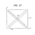
- FIG. 27 is a plan view illustrating the vacuuming face of the vacuuming collet illustrated in FIG. 26 ;
- FIG. 28 is a sectional view of a substantial part, explaining a void formed between a semiconductor chip and a wiring substrate;
- FIG. 29 is an explanatory drawing illustrating an example of a vacuum supply line for supplying reduced pressure to a vacuuming collet
- FIG. 30 is an explanatory drawing illustrating an example of a vacuum supply line for supplying reduced pressure to a vacuuming collet
- FIG. 31 is a sectional view of a wiring substrate, illustrating a pellet bonding step for a semiconductor chip
- FIG. 32 is a sectional view of a wiring substrate, illustrating steps for laminating semiconductor chips and wire bonding
- FIG. 33 is a sectional view of a wiring substrate, illustrating a step for plastic molding semiconductor chips
- FIG. 34 is an explanatory drawing illustrating an example of a vacuum supply line for supplying reduced pressure to a vacuuming collet used in the fabrication of a semiconductor device in a second embodiment of the invention
- FIG. 35 is a perspective view of a substantial part of a bonding stage used in a temporary pressure bonding step for semiconductor chips in a fabrication process for a semiconductor device in a third embodiment of the invention.
- FIG. 36 is a perspective view of a substantial part illustrating the way a wiring substrate and semiconductor chips are disposed over the bonding stage illustrated in FIG. 35 ;
- FIG. 37 is a plan view illustrating in close-up a chip disposed over the bonding stage illustrated in FIG. 35 ;
- FIG. 38 is a sectional view of a substantial part illustrating in close-up an area in proximity to a projection provided on a bonding stage in a situation in which a wiring substrate and a chip are disposed over the bonding stage illustrated in FIG. 35 ;
- FIG. 39 is a sectional view of a substantial part, explaining the structure of a vacuuming collet used in the fabrication of a semiconductor device in a fourth embodiment of the invention.
- FIG. 40 is a sectional view of a substantial part, explaining the structure of a vacuuming collet used in the fabrication of a semiconductor device in the fourth embodiment of the invention.
- FIG. 41 is a plan view explaining the structure of a vacuuming collet used in the fabrication of a semiconductor device in a fifth embodiment of the invention.
- FIG. 42 is a sectional view of a substantial part, explaining the structure of a vacuuming collet used in the fabrication of a semiconductor device in the fifth embodiment of the invention.
- FIG. 43 is a sectional view of a substantial part, explaining the structure of a vacuuming collet used in the fabrication of a semiconductor device in the fifth embodiment of the invention.
- FIG. 44 is an enlarged sectional view of an area in proximity to the upper face of a vacuum chuck piece, explaining a method for unsticking a semiconductor chip when a plunge-up pin is used;
- FIG. 45 is an enlarged sectional view of an area in proximity to the upper face of a vacuum chuck piece, explaining a method for unsticking a semiconductor chip when a horn for emitting ultrasonic waves is used;
- FIG. 46 is a flowchart illustrating how to cope with a failure to pick up a chip from a dicing tape that occurs in the fabrication process for a semiconductor device in a sixth embodiment of the invention.
- FIG. 47 is a flowchart of substantial steps illustrating how to cope with a failure to pick up a chip from a dicing tape that occurs in the fabrication process for a semiconductor device in a seventh embodiment of the invention.
- FIG. 48 is a sectional view of a substantial part of a horn used in the fabrication of a semiconductor device in an eighth embodiment of the invention.
- FIG. 49 is a plan view illustrating the tip of the horn illustrated in FIG. 48 ;
- FIG. 50 is a plan view illustrating the comparison between the tip of the horn illustrated in FIG. 48 and FIG. 49 and a chip to be unstuck for size;
- FIG. 51 is a sectional view of a substantial part of a horn used in the fabrication of a semiconductor device in a ninth embodiment of the invention.
- FIG. 52 is a plan view illustrating the tip of the horn illustrated in FIG. 51 ;
- FIG. 53 is a plan view illustrating the comparison between the tip of the horn illustrated in FIG. 51 and FIG. 52 and a chip to be unstuck for size;
- FIG. 54 is a top view of a dimensional measurement jig for magazines used in the fabrication of a semiconductor device in a 10th embodiment of the invention.
- FIG. 55 is a side view of a dimensional measurement jig for magazines used in the fabrication of a semiconductor device in the 10th embodiment of the invention.
- FIG. 56 is a side view of a magazine used in the fabrication of a semiconductor device in the 10th embodiment of the invention.
- FIG. 57 is a flowchart illustrating the steps from the step of measuring the dimensions of a magazine used in the fabrication of a semiconductor device in the 10th embodiment of the invention to the step of moving the magazine to a wiring substrate unloading position with variation in the dimensions of the magazine taken into account;
- FIG. 58 is a top view of a dimensional measurement jig for magazines, explaining the details of the steps in the flowchart illustrated in FIG. 57 ;
- FIG. 59 is a side view of a dimensional measurement jig for magazines, explaining the details of the steps in the flowchart illustrated in FIG. 57 ;
- FIG. 60 is a top view of a dimensional measurement jig for magazines, explaining the details of the steps in the flowchart illustrated in FIG. 57 ;
- FIG. 61 is a side view of a dimensional measurement jig for magazines, explaining the details of the steps in the flowchart illustrated in FIG. 57 ;
- FIG. 62 is a side view of a dimensional measurement jig for magazines, explaining the details of the steps in the flowchart illustrated in FIG. 57 ;
- FIG. 63 is a side view of a dimensional measurement jig for magazines, explaining the details of the steps in the flowchart illustrated in FIG. 57 ;
- FIG. 64 is a top view of a dimensional measurement jig for magazines, explaining the details of the steps in the flowchart illustrated in FIG. 57 ;
- FIG. 65 is a side view of a dimensional measurement jig for magazines, explaining the details of the steps in the flowchart illustrated in FIG. 57 ;
- FIG. 66 is a side view of a dimensional measurement jig for magazines, explaining the details of the steps in the flowchart illustrated in FIG. 57 ;
- FIG. 67 is a top view of a dimensional measurement jig for magazines, explaining the details of the steps in the flowchart illustrated in FIG. 57 ;
- FIG. 68 is a side view of a dimensional measurement jig for magazines, explaining the details of the steps in the flowchart illustrated in FIG. 57 ;
- FIG. 69 is a top view of a dimensional measurement jig for magazines, explaining the details of the steps in the flowchart illustrated in FIG. 57 ;
- FIG. 70 is a side view of a dimensional measurement jig for magazines, explaining the details of the steps in the flowchart illustrated in FIG. 57 ;
- FIG. 71 is a top view of a dimensional measurement jig for magazines, explaining the details of the steps in the flowchart illustrated in FIG. 57 ;
- FIG. 72 is a side view of a dimensional measurement jig for magazines, explaining the details of the steps in the flowchart illustrated in FIG. 57 ;
- FIG. 73 is a top view of a dimensional measurement jig for magazines, explaining the details of the steps in the flowchart illustrated in FIG. 57 ;
- FIG. 74 is a side view of a dimensional measurement jig for magazines, explaining the details of the steps in the flowchart illustrated in FIG. 57 ;
- FIG. 75 is a side view of a dimensional measurement jig for magazines, explaining the details of the steps in the flowchart illustrated in FIG. 57 ;
- FIG. 76 is a side view of a dimensional measurement jig for magazines, explaining the details of the steps in the flowchart illustrated in FIG. 57 ;
- FIG. 77 is a side view of a dimensional measurement jig for magazines, explaining the details of the steps in the flowchart illustrated in FIG. 57 ;
- FIG. 78 is a flowchart illustrating the steps from the step of measuring the dimensions of a magazine used in the fabrication of a semiconductor device in an 11th embodiment of the invention to the step of moving the magazine to a wiring substrate unloading position with variation in the dimensions of the magazine taken into account.
- Wafer refers to an insulating, anti-insulating, or semiconductor substrate, including a single crystal silicon substrate (usually, in substantially circular planar shape), an SOI (Silicon On Insulator) substrate, an epitaxial substrate, a sapphire substrate, a glass substrate, and the like or a composite substrate of them used in the fabrication of a semiconductor element or an integrated circuit.
- the semiconductor device cited in this specification includes not only those fabricated over a semiconductor or insulator substrate, such as a silicon wafer or sapphire substrate, but also those formed over any other insulating substrate of, for example, glass, including TFT (Thin Film Transistor) and STN (Super-Twisted-Nematic) liquid crystals, and the like unless otherwise stated.
- Device surface or element formation surface refers to the principal surface of a wafer on which a device pattern corresponding to multiple chip areas is formed by lithography.
- Collet refers to a vacuum chuck tool used to transport chips one by one after a wafer is divided into the individual chips by dicing or the like.
- Chip plunge-up refers to the following operation performed when, after a wafer is divided into individual chips, the chips are separated, vacuumed, and transported: plunging up a chip from the rear surface side of the wafer over an adhesive tape stuck to the rear surface with a needle-like pin or the like.
- Magazine refers to a case for supplying and housing mounting boards or the like on which a chip is to be mounted. It is set in the loader and unloader of equipment in which die bonding, wire bonding, plastic molding, or any other like step is carried out.
- each embodiment will be divided into multiple sections or embodiments if necessary for the sake of convenience. Unless explicitly stated otherwise, they are not unrelated to one another, and they are in such a relation that one is a modification, details, supplementary explanation, or the like of part or all of the other.
- a silicon member includes not only pure silicon but also an additive impurity, binary, ternary, and other like alloys (e.g., SiGe), and the like unless explicitly stated otherwise.
- the invention is applied to the fabrication of a semiconductor package in which a chip is mounted over a wiring substrate. Description will be given to the fabrication method in the order of process steps with reference to FIG. 1 to FIG. 33 .
- integrated circuits are formed in the principal surface of a wafer 1 W formed of single crystal silicon illustrated in FIG. 1 . Thereafter, the integrated circuit formed in each of the multiple chip formation areas (chip areas) 1 CA partitioned by lattice-shaped scribe lines (parting areas) is subjected to an electrical test to determine its acceptability.
- the chip formation areas 1 CA in the wafer 1 W used in the first embodiment are in square planar shape with their longitudinal length equal to their lateral length.
- a back grind tape 3 for integrated circuit protection is stuck to the integrated circuit formation surface (on the lower side of the drawing) of the wafer 1 W.
- the rear surface (on the upper side of the drawing) of the wafer 1 W is ground with a grinder.
- the damage layer on the rear surface produced during this grinding is removed by wet etching, dry polishing, plasma etching, or any other like method to reduce the thickness of the wafer 1 W to a value not more than 100 ⁇ m, for example, a value of 50 ⁇ m to 90 ⁇ m or so.
- the processing methods such as wet etching, dry polishing, and plasma etching have the following effects: while in these methods, the speed of processing that proceeds in the direction of the thickness of a wafer is lower than the speed of grinding by a grinder, the damage it does to the interior of the wafer is minor as compared with damage done by grinding; in addition, a damage layer produced in the wafer as the result of grinding by the grinder can be removed; and this makes the wafer 1 W and chips resistant to cracking.
- the back grind tape 3 is removed, and then DAF (not shown) is stuck to the rear surface (the surface opposite the integrated circuit formation surface) of the wafer 1 W, as illustrated in FIG. 3 .
- the DAF functions as adhesive when a chip is mounted over a wiring substrate.
- a dicing tape (adhesive tape) 4 is stuck to the DAF, and in this state, the peripheral portion of the dicing tape 4 is fixed on a wafer ring 5 . Instead, the wafer 1 W is often stuck to a dicing tape 4 to which DAF has been stuck beforehand.
- the dicing tape 4 is obtained by: applying an adhesive compound to the surface of a tape base material formed of polyolefin (PO), polyvinyl chloride (PVC), polyethylene terephthalate (PET), or the like to provide it with adherence (tackness); and cutting it in a circular shape.
- An UV cure adhesive compound is also often used.
- the wafer 1 W is diced using a dicing blade 6 as illustrated in FIG. 4 , and the chip formation areas 1 CA are thereby divided into square chips 1 C.
- the dicing tape 4 is cut by a few tens of ⁇ m in the direction of its thickness.
- an UV cure adhesive tape is used as the dicing tape 4
- the dicing tape 4 is irradiated with ultraviolet rays to reduce the adhesive force of the adhesive compound prior to the chip 1 C unsticking step described later.
- a retaining plate 7 is disposed above the dicing tape 4 fixed on the wafer ring 5 and an expand ring 8 is disposed under the dicing tape.
- the retaining plate 7 is pressed against the upper face of the wafer ring 5 , and at the same time, the peripheral portion of the rear surface of the dicing tape 4 is pushed upward by the expand ring 8 .
- the adhesive face of the dicing tape 4 receives high tension (first tension) directed from its central portion to its peripheral portion; therefore, the dicing tape is stretched taut in the horizontal direction.
- the expand ring 8 is positioned on the stage 101 of the chip unsticking apparatus 100 illustrated in FIG. 8 , and is held horizontal.
- a vacuum chuck piece 102 In the center of the stage 101 , there is disposed a vacuum chuck piece 102 that is moved in the horizontal direction and in the vertical direction by a drive mechanism (not shown).
- the dicing tape 4 is so held that its rear surface is opposed to the upper face of the vacuum chuck piece 102 .
- FIG. 9 is a sectional view of the vacuum chuck piece 102 ;
- FIG. 10 is an enlarged sectional view of an area in proximity to the upper face of the vacuum chuck piece 102 ; and
- FIG. 11 is an enlarged perspective view of an area in proximity to the upper face of the vacuum chuck piece 102 .
- the upper face of the vacuum chuck piece 102 is provided at its peripheral portion with multiple vacuum ports 103 and multiple grooves 104 concentrically formed. More vacuum ports 103 may be disposed in the entire upper face of the vacuum chuck piece instead of providing the grooves 104 .
- the interior of each vacuum port 103 and groove 104 is depressurized with a suction force of ⁇ 90 kPa to ⁇ 60 kPa by a suction mechanism (not shown) when the vacuum chuck piece 102 is moved up to bring its upper face into contact with the rear surface of the dicing tape 4 . At this time, the rear surface of the dicing tape 4 is vacuumed downward and is brought into tight contact with the upper face of the vacuum chuck piece 102 .
- an unfavorable phenomenon can occur when the dicing tape 4 is vacuumed downward.
- the interface between the adjacent chip 1 C and the dicing tape 4 positioned under the chip can be broken into two above the groove 104 .
- this break is likely to occur.
- an adjacent chip 1 C can drop from the dicing tape 4 while the chip (first semiconductor chip) 1 C to be unstuck is being unstuck from the dicing tape 4 .
- the width or depth of the grooves 104 is reduced as much as possible so that a void will not formed between the dicing tape 4 positioned under adjacent chips 1 C and the upper face of the vacuum chuck piece 102 .
- first block 110 A In the central part of the vacuum chuck piece 102 , there are incorporated a first block 110 A, a second block 110 B, and a third block 110 C that plunge up the dicing tape 4 .
- first block 110 A largest in diameter
- second block 110 B Inside the first block 110 A largest in diameter, there is disposed the second block 110 B smaller in diameter than the first block, and inside the second block, there is disposed the third block 110 C smallest in diameter.
- the three blocks, the first block 110 A, second block 110 B, and third block 110 C are so constructed that they are moved up and down in conjunction with the following: a first helical compression spring 111 A placed between the first block 110 A positioned outside and the second block 110 B positioned in the middle; a second herical compression spring 111 B placed between the second block 110 B positioned in the middle and the third block 110 C positioned inside and having a higher spring constant than that of the first herical compression spring 111 A; and a pusher 112 coupled with the third block 110 C and moved up and down by a drive mechanism, not shown.
- the first block 110 A largest in diameter and positioned outside, whose diameter is slightly (e.g., 0.5 mm to 3 mm or so) smaller than that of the chip 1 to be unstuck is used.
- the chip 1 C is square, for example, it is desirable to use a slightly smaller square block.
- the chip 1 C is rectangular, it is desirable to use a slightly smaller rectangular block.
- the corners that form the periphery of the upper face of the first block 110 A are positioned slightly inside the outer edge of the chip 1 C. Therefore, force for separating the chip 1 C and the dicing tape 4 can be concentrated on a place (the outermost portion of the chip 1 C) where the separation between the chip 1 C and the dicing tape 4 starts.
- the upper face of the first block 110 A and the dicing tape 4 it is desirable that the upper face should be a flat surface or a surface having a large radius of curvature.
- the area of contact between the upper face of the first block 110 A and the dicing tape 4 is small, large bending stress is concentrated on the peripheral portion of the chip 1 C that is supported from below by the upper face of the first block 110 A. As a result, the peripheral portion of the chip 1 C can crack.
- the second block 110 B positioned in the middle, disposed inside the first block 110 A has a diameter 1 mm to 3 mm or so smaller than that of the first block 110 A.
- the third block 110 C smallest in diameter and disposed inside the second block 110 B, has a diameter 1 mm to 3 mm or so further smaller than that of the second block 110 B positioned in the middle.
- the second block 110 B positioned in the middle and the third block 110 C positioned outside are respectively formed in a columnar shape in consideration of ease of machining and the like. Instead, they may be formed in a quadratic prism shape similarly with the first block 110 A positioned outside or in a shape approximate thereto.
- the upper faces of the three blocks, the first block 110 A, second block 110 B, and third block 110 C are identical with one another in height in the initial state.
- the initial state is a state in which none of the first block 110 A, second block 110 B, and third block 110 C is in operation.
- the upper faces of the three blocks are also flush with the peripheral portion of the upper face of the vacuum chuck piece 102 .
- a gap (S) is provided between the peripheral portion of the vacuum chuck piece 102 and the first block 110 A positioned outside and between the three blocks, the first block 110 A, second block 110 B, and third block 110 C.
- the interior of these gaps (S) is depressurized by a suction mechanism, not shown.
- the central portion (first block 110 A, second block 110 B, and third block 110 C) of the vacuum chuck piece 102 is moved to directly under one chip 1 C to be unstuck (the chip 1 C positioned in the center of the drawing); at the same time, a vacuuming collet 105 is moved to above this chip 1 C.
- the vacuuming collet 105 supported by a transferring mechanism (not shown) is provided in the center of its bottom face with a vacuum chuck hole 106 whose interior is depressurized.
- the vacuuming collet is so constructed that it is capable of selectively vacuuming and holding only one chip 1 C to be unstuck.
- the vacuum chuck piece 102 is moved up to bring its upper face into contact with the rear surface of the dicing tape 4 , and further the interior of the above-mentioned vacuum ports 103 , grooves 104 , and gaps (S) is depressurized.
- the dicing tape 4 in contact with the chip 1 C to be unstuck is brought into tight contact with the upper faces of the first block 110 A, second block 110 B, and third block 110 C.
- the dicing tape 4 in contact with other chips 1 C adjacent to this chip 1 C is brought into tight contact with the peripheral portion of the upper face of the vacuum chuck piece 102 .
- the vacuum chuck piece 102 is slightly (e.g., 400 ⁇ m or so) is plunged up.
- tension can be further applied to the dicing tape 4 to which tension has been horizontally applied by the above-mentioned retaining plate 7 and expand ring 8 . Therefore, the vacuum chuck piece 102 and the dicing tape 4 can be more reliably brought into tight contact with each other.
- the vacuuming collet 105 is moved down to bring the bottom face of the vacuuming collet 105 into contact with the upper face of the chip 1 C to be unstuck.
- the chip 1 C is vacuumed with a suction force of 80 kPa or so and the chip 1 C is lightly held down.
- the three blocks, the first block 110 A, second block 110 B, and third block 110 C are simultaneously plunged up to apply upward load to the rear surface of the dicing tape 4 and push up the chip 1 C and the dicing tape 4 .
- the rear surface of the chip 1 C is supported by the upper faces (contact faces) of the first block 110 A, second block 110 B, and third block 110 C through the dicing tape 4 to lessen the bending stress exerted on the chip 1 C.
- the periphery (corners) of the upper face of the first block 110 A is disposed inside the periphery of the chip 1 C.
- FIG. 15 is an enlarged perspective view of an area in proximity to the upper face of the vacuum chuck piece 102 . (The chip 1 C or the dicing tape 4 is not shown.)
- the plunging amount (stroke) of each of the first block 110 A, second block 110 B, and third block 110 C is, for example, 0.4 mm or so.
- the stroke may be varied depending on the angle required for separation.
- the adhesive compound applied to the dicing tape 4 differs in adhesive force from manufacturer to manufacturer or from product class to product class. Therefore, when an adhesive compound high in adhesive force is used, it is required to increase the plunging amount to ensure an angle required for separation even though the chips 1 C are identical in size.
- the bending stress in a direction orthogonal to the periphery of the chip is made smaller than the bending stress in a direction parallel with the periphery of the chip.
- the extreme peripheral portion of a chip 1 C there remains a fine crack produced when the wafer 1 W is diced using the above-mentioned dicing blade 6 .
- the first block 110 A whose upper face slightly smaller in size than the chip 1 C is used to evenly apply load slightly inside the extreme peripheral portion of the chip 1 C. Therefore, this problem can be avoided, and further the entire circumferential portion of the chip 1 C can be evenly unstuck from the dicing tape 4 .
- the pusher 112 is pushed upward to push up the third block 110 C, positioned inside, coupled with the pusher 112 as illustrated in FIG. 16 .
- the second block 110 B positioned in the middle is pushed up by spring force from the helical compression spring 111 B placed between the third block 110 C positioned inside and the second block 110 B positioned in the middle.
- the first block 110 A positioned outside is pushed up by spring force from the helical compression spring 111 A placed between the first block 110 A positioned outside and the second block 110 B positioned in the middle.
- the three blocks, the first block 110 A, second block 110 B, and third block 110 C are simultaneously pushed up.
- part (surface indicated by arrows in the drawing) of the first block 110 A positioned outside is brought into contact with the peripheral portion of the vacuum chuck piece 102 , the ascent of the first block 110 A, second block 110 B, and third block 110 C is stopped.
- the most part of the chip 1 C to be unstuck is supported by the upper faces of the three blocks, the first block 110 A, second block 110 B, and third block 110 C.
- separation efficiently proceeds in the interface between the chip 1 C and the dicing tape 4 .
- the pusher 112 pushes up the block 110 C.
- the pusher pushes it up with so weak force that the helical compression spring 111 A whose spring force is weak will not be compressed.
- the second block 110 B positioned in the middle or the third block 110 C positioned inside is not further plunged up.
- the helical compression spring 111 A is required to have spring force of at least such a level as to lift the first block 110 A against the tension of the dicing tape 4 . If the spring force of the helical compression spring 111 A is lower than the tension of the dicing tape 4 , the first block 110 A positioned outside is not lifted even when the pusher 112 is pushed up. Therefore, the chip 1 C cannot be supported any more by the upper face of the first block 110 A positioned outside. In this case, sufficient stress cannot be concentrated on the starting point of separation between the chip 1 C and the dicing tape 4 . This can result in some problem. For example, the speed of separation may be reduced, or excessive bending stress may be applied to the chip 1 C, which may be in turn broken.
- FIG. 17 is an enlarged perspective view illustrating an area in proximity to the upper face of the vacuum chuck piece 102 at this time (The chip 1 C or the dicing tape 4 is not shown.)
- the pusher 112 is pushed up to further push up the third block 110 C coupled with the pusher 112 , as illustrated in FIG. 19 .
- the second block 110 B positioned in the middle is pushed up by spring force from the helical compression spring 111 B. Therefore, the two blocks, the second block 110 B and the third block 110 C positioned inside are simultaneously pushed up.
- part (surface indicated by arrows in the drawing) of the second block 110 B positioned in the middle is brought into contact with the first block 110 A positioned outside, the ascent of the second block 110 B and the third block 110 C positioned inside is stopped.
- the force of the pusher 112 for pushing up the third block 110 C is set to such a magnitude that the helical compression spring 111 A whose spring force is weak is compressed but the helical compression spring 111 B whose spring force is strong is not compressed.
- the third block 110 C positioned inside is not further plunged up.
- the following measure is taken to facilitate the separation between the chip 1 C and the dicing tape 4 : the interior of the gaps (S) between the first block 110 A, second block 110 B, and third block 110 C is depressurized, and the dicing tape 4 in contact with the chip 1 C is thereby vacuumed downward. Further, the interior of the grooves 104 is depressurized to bring the dicing tape 4 in contact with the peripheral portion of the upper face of the vacuum chuck piece 102 into tight contact with the upper face of the vacuum chuck piece 102 . (Refer to FIG. 17 .)
- FIG. 21 is an enlarged perspective view illustrating an area in proximity to the upper face of the vacuum chuck piece 102 at this time (The chip 1 C or the dicing tape 4 is not shown.)
- the third block 110 C is pushed up by so strong force that the helical compression spring 111 B is compressed, as illustrated in FIG. 22 .
- the separation between the chip 1 C and the dicing tape 4 proceeds in the area outside the periphery (corners) of the upper face of the third block 110 C in contact with the dicing tape 4 .
- the third block 110 C is pulled downward and at the same time the vacuuming collet 105 is pulled upward. This completes the operation of unsticking the chip 1 C from the dicing tape 4 .
- the upper face of the third block 110 C need be reduced in area to the extent that when the third block 110 C is plunged up, the chip 1 C is unstuck from the dicing tape 4 by only suction force from the vacuuming collet 105 . If the area of the upper face of the third block 110 C is large, the area of contact between the chip 1 C and the dicing tape 4 is also large, and this increase the adhesive force between them. Therefore, the chip 1 C cannot be unstuck from the dicing tape 4 by only the force of the vacuuming collet 105 for vacuuming the chip 1 C.
- the chip 1 C can be broken. To cope with this, it is desirable to take the following measure to prevent high load from being applied to a narrow area in the chip 1 C when the block 110 c is plunged up: the plunging speed is reduced; the time for which the upper face of the third block 110 C is in contact with the dicing tape 4 is shortened; or the plunging amount (stroke) of the third block 110 C is reduced (e.g., by 0.2 mm to 0.4 mm or so).
- One effective method for increasing the suction force of the vacuuming collet 105 is to reduce the speed at which the vacuuming collet 105 is pulled up. If the vacuuming collet 105 is rapidly pulled up with part of the chip 1 C in tight contact with the dicing tape 4 , a gap is produced between the bottom face of the vacuuming collet 105 and the upper face of the chip 1 C. Since the degree of vacuum in the vacuuming collet 105 is consequently reduced, the force for vacuuming the chip 1 C is reduced. Meanwhile, when the speed at which the vacuuming collet 105 is pulled up is reduced, the time required to unstick the chip 1 C from the dicing tape 4 is lengthened.
- the speed at which the vacuuming collet 105 is pulled up is made variable; when pull-up is started, the pull-up speed is lowered to ensure sufficient suction force; and when the area of contact between the chip 1 C and the dicing tape 4 is reduced to some extent, the pull-up speed is increased to prevent the unsticking time from being lengthened.
- Making the area of the bottom face of the vacuuming collet 105 larger than the area of the upper face of the third block 110 C is another effective method for increasing the suction force of the vacuuming collet 105 .
- the suction force of the vacuuming collet 105 By increasing the suction force of the vacuuming collet 105 as mentioned above, the following can be implemented: even when the area of contact between the chip 1 C and the dicing tape 4 is relatively large, the chip 1 C can be unstuck from the dicing tape 4 by only the suction force of the vacuuming collet 105 . Therefore, the unsticking time can be shortened and further the above problem that will occur if the area of the upper face of the third block 110 C is reduced can be avoided.
- the vacuuming collet 105 When the third block 110 C is pulled down with the chip 1 C held down by the vacuuming collet 105 , the vacuuming collet 105 is also moved downward. Therefore, there is the possibility that the chip 1 C is hit against the third block 110 C and broken. When the third block 110 C is pulled down, to cope with this, it is desirable to pull down the vacuuming collet 105 immediately before or fix the position of the vacuuming collet 105 at least so that it will not be moved downward.
- the chip 1 C is as thin as approximately 100 ⁇ m or less. Especially, when it is as thin as 75 ⁇ m or less, it is likely to be warped by the suction force of the vacuuming collet 105 after it is unstuck from the dicing tape 4 by the vacuuming collet 105 .
- FIG. 24 is a sectional view of a substantial part of a bonding head 107 including the vacuuming collet 105 . It shows the chip 1 C vacuumed into a vacuum chuck hole 106 formed in the vacuuming collet 105 and warped.
- FIG. 25 is a plan view illustrating the vacuum chuck surface (surface brought into contact with a chip 1 C) of the vacuuming collet 105 .
- FIG. 24 corresponds to a section taken along line A-A of FIG. 25 .
- FIG. 26 and FIG. 27 respectively illustrate a section and a plane of a vacuuming collet 105 of such structure that its vacuum chuck surface is provided with grooves 105 H in addition to the vacuum chuck hole 106 .
- a chip 1 C is also vacuumed into the groove 105 H and warped. If such a warped chip 1 C is placed and mounted (bonded) over a wiring substrate 11 by the vacuuming collet 105 , it is mounted over the wiring substrate 11 as is warped.
- a void is prone to be formed.
- a mount (adhesion) failure occurs in the chip 1 C.
- a chip 1 C is broken away from the wiring substrate 11 by expansion of the void KH or the like.
- a vacuum supply line that connects to the vacuum chuck hole 106 formed in the bottom face of the vacuuming collet 105 and supplies the vacuuming collet 105 with reduced pressure for vacuum chucking a chip 1 C is constructed of two systems illustrated in FIG. 29 . More specific description will be given.
- the first embodiment is so constructed that the following pipes are connected to the vacuuming collet 105 : a pipe (first vacuum supply system) 121 for supplying the vacuuming collet 105 with a vacuum ( ⁇ 80 kPa or so) that provides suction force (first suction force) when a chip 1 C is unstuck from a dicing tape 4 and transported to a mounting position on a wiring substrate 11 ; and a pipe (second vacuum supply system) 122 for supplying the vacuuming collet 105 with a vacuum that provides suction force (second suction force) when a chip 1 C is mounted over a wiring substrate 11 .
- a pipe (first vacuum supply system) 121 for supplying the vacuuming collet 105 with a vacuum ( ⁇ 80 kPa or so) that provides suction force (first suction force) when a chip 1 C is unstuck from a dicing tape 4 and transported to a mounting position on a wiring substrate 11 ; and a pipe (second vacuum supply system) 122 for supplying
- the intensity of a vacuum supplied through the pipe 122 only has to be sufficient to prevent a chip 1 C from being warped and a chip 1 C from dropping from the vacuuming collet 105 .
- it is ⁇ 10 kPa to 0 kPa or so, preferably, ⁇ 1 kPa to 0 kPa or so.
- the intensity of a vacuum is preferably ⁇ 5 kPa to 0 kPa or so.
- the pipes 121 , 122 respectively have valves 123 , 124 such as electromagnetic valves installed therein. The intensity of a vacuum (suction force) supplied to the vacuuming collet 105 can be controlled by opening or closing these valves 123 , 124 .
- the force of the vacuuming collet 105 for vacuuming the chip 1 C is reduced, and the warpage caused in the chip 1 C can be eliminated.
- the formation of the above-mentioned void KH can be suppressed. (Refer to FIG. 28 for the void KH.)
- the intensity of a vacuum supplied through the pipe 121 is reduced by the amount equivalent to the intensity of a vacuum supplied through the pipe 122 .
- both the valves 123 , 124 are opened.
- the vacuuming collet 105 is supplied with a vacuum ( ⁇ 80 kPa or so) that provides suction force when the chip 1 C is unstuck from a dicing tape 4 and transported to the mounting position on the wiring substrate 11 .
- a vacuum ⁇ 80 kPa or so
- the chip 1 C unstuck from the dicing tape 4 as mentioned above is vacuumed and held by the vacuuming collet 105 and transported to the next step (pellet bonding step).
- the next chip 1 C is unstuck from the dicing tape 4 following the procedure illustrated in FIG. 12 to FIG. 23 .
- chips 1 C are unstuck from the dicing tape 4 one by one, following the same procedure.
- the chip 1 C transported to the pellet bonding step is mounted in a mounting position (chip mounting area) on a wiring substrate (mounting board) 11 through DAF 10 stuck to its rear surface beforehand, by thermocompression.
- a void KH can be prevented from being formed between the chip 1 C and the wiring substrate 11 .
- FIG. 28 for the void KH. That is, the chip 1 C can be mounted (bonded) over the wiring substrate 11 with reliability. Subsequently, it is electrically connected with an electrode 13 on the wiring substrate 11 through an Au wire 12 .
- the void KH can be expanded by heat produced when the Au wire 12 is connected. This can break the chip 1 C away from the wiring substrate 11 .
- a measure is taken to prevent the formation of a void KH; therefore, a problem of the separation of the chip 1 C or the like can be prevented from occurring.
- a second chip 14 is laminated over the chip 1 C mounted over the wiring substrate 11 , through DAF 10 or the like, and it is electrically connected with an electrode 16 on the wiring substrate 11 through an Au wire 15 or the like.
- the second chip 14 is a silicon chip in which an integrated circuit different from that of the chip 1 C is formed.
- the second chip is unstuck from the dicing tape 4 by the above-mentioned method, and then transported to the pellet bonding step and laminated in a mounting position (chip mounting area) over the chip 1 C.
- the chips are thinned because of demands for reduction in the size and thickness of packages.
- a void KH can be especially effectively prevented from being formed between the chip 1 C and the wiring substrate 11 and between the second chip 14 and the chip 1 C. (Refer to FIG. 28 for the void KH.)
- the wiring substrate 11 is transported to a molding step.
- the chip 1 C and the second chip 14 are sealed with molding resin 17 as illustrated in FIG. 33 , and a laminate package 18 is thereby completed.
- a measure is taken for preventing a void KH from being formed between the chip 1 C and the wiring substrate 11 and between the second chip 14 and the chip 1 C.
- the molding step therefore, the following problem can be prevented from occurring: a void KH is expanded by heat used during the sealing operation, and the chip 1 C and the second chip 14 are thereby separated from each other.
- three blocks, the first block 110 A, second block 110 B, and third block 110 C are used to unstick a chip.
- the number of blocks is not limited to three, and four or more blocks may be used when the size of a chip 1 C to be unstuck is large. Or, two blocks may be used when the size of a chip 1 C to be unstuck is very small.
- the vacuum supply line described in relation to the first embodiment is constructed otherwise. (Refer to FIG. 29 and FIG. 30 for the vacuum supply line of the first embodiment.)
- the constructions of the other steps and members are the same as those in the first embodiment.
- FIG. 34 is an explanatory drawing of a vacuum supply line for supplying reduced pressure to the vacuuming collet 105 in the second embodiment.
- the vacuum supply line is formed of two systems.
- what is supplied through the pipe 122 is not a vacuum but air.
- the intensity of air supplied through the pipe (first air supply system) 122 is set so as to supply an appropriately smaller flow rate as compared with the pull-in flow rate on the vacuum side (the pipe 121 ) to control the vacuum pressure.
- the vacuum pull-in flow rate of the pipe 121 is approximately 20 L (liters)/min, for example, air is supplied through the pipe 122 at approximately 19 L (liters)/min to reduce the vacuum pressure.
- the valve 123 When a chip 1 C is unstuck from a dicing tape 4 and transported to a mounting position on a wiring substrate 11 , the valve 123 is opened and the valve 124 is closed as in the first embodiment.
- the vacuuming collet 105 is provided with a vacuum ( ⁇ 80 kPa or so) that provides suction force when the chip 1 C is unstuck from the dicing tape 4 and transported to the mounting position on the wiring substrate 11 .
- both the valves 123 , 124 are opened. Thus, both a vacuum and air are supplied.
- the vacuuming collet 105 Since the pull-in flow rate of the vacuum supplied through the pipe 121 is higher than the supply flow rate of the air supplied through the pipe 122 , the vacuuming collet 105 is consequently supplied with suction force (vacuum).
- the intensity of suction force (vacuum) supplied to the vacuuming collet 105 at this time is sufficient to prevent warpage from being caused in the chip 1 C and the chip 1 C from dropping from the vacuuming collet 105 . It is ⁇ 10 kPa to 0 kPa or so, preferably, ⁇ 1 kPa to 0 kPa or so.
- the intensity of suction force is preferably ⁇ 5 kPa to 0 kPa or so.
- the force of the vacuuming collet 105 for vacuuming the chip 1 C is reduced, and the warpage caused in the chip 1 C can be eliminated.
- the formation of a void KH can be suppressed as in the first embodiment. (Refer to FIG. 28 for the void KH.)
- the third embodiment is so constructed that the thermocompression bonding step as the pellet bonding step for a chip 1 C, described in relation to the first and second embodiments is divided into two stages: a temporary pressure bonding step for bonding only part of a chip 1 C by thermocompression; and a proper pressure bonding step for bonding the whole of the chip 1 C by thermocompression. This is the same with the pellet bonding step for the second chip 14 .
- FIG. 35 is a perspective view of a substantial part of a bonding stage KBS used at the above temporary pressure bonding step.
- FIG. 36 is a perspective view of a substantial part illustrating the way a wiring substrate 11 and chips 1 C are placed over the bonding stage KBS.
- FIG. 37 is a plan view illustrating in close-up a chip 1 C placed over the bonding stage (first bonding stage) KBS.
- FIG. 38 is a sectional view of a substantial part illustrating in close-up an area in proximity to a protrusion (pressure applying jig) TK in a situation in which a wiring substrate 11 and a chip 1 C are placed over the bonding stage KBS. As illustrated in FIG. 37 and FIG.
- this protrusion TK applies pressure to an area (temporary pressure bonding area) in the center of the rear surface of a chip 1 C through a wiring substrate 11 at the temporary pressure bonding step for the chip 1 C.
- the area hatched in FIG. 37 refers to an area to which pressure is applied by the protrusion TK.
- the protrusion TK is formed beforehand so that the following is implemented: the area to which pressure is applied by the protrusion TK is 10% to 40% or so, preferably, 25% or so of the rear surface of the chip 1 C.
- the proper pressure bonding step is carried out to bond the entire rear surface of the chip 1 C to the wiring substrate 11 by thermocompression.
- warpage in the chip 1 C has been already eliminated through the above-mentioned temporary pressure bonding step. Therefore, the entire rear surface of the chip 1 C can be thermocompression bonded to the wiring substrate 11 with reliability.
- the control method for the suction force of the vacuuming collet 105 for vacuuming chips 1 C may be combined with the above-mentioned pellet bonding step of the third embodiment. In this case, the formation of a void KH can be more effectively suppressed.
- FIG. 39 is a sectional view of a substantial part of a bonding head 107 used in the fourth embodiment.
- the bonding head 107 in the fourth embodiment is formed of: a vacuuming collet 105 that is brought into contact with the chip 1 C or second chip 14 , described in relation to the first embodiment, during a pellet bonding step; a collet holder 105 G for holding the vacuuming collet 105 ; an inclination adjusting mechanism (head section) 105 A on which the collet holder 105 G is installed; a supporting seat (supporting seat section) 105 B brought into contact with the inclination adjusting mechanism 105 A; a magnet 105 C that holds the head section through the supporting seat 105 B by magnetic force; and the like.
- a support section for holding the inclination adjusting mechanism 105 A is formed of the supporting seat 105 B and the magnet 105 C.
- the supporting seat 105 B is also formed of a magnetic metal, such as high-speed tool steel and alloy high-speed tool steel. It has its face (first surface) brought into contact with the inclination adjusting mechanism 105 A spherically machined in agreement with the shape of the spherically machined surface (second surface) of the inclination adjusting mechanism 105 A.
- the magnet 105 C is formed of, for example, a neodymium magnet.
- the inclination adjusting mechanism 105 A It holds the inclination adjusting mechanism 105 A through the supporting seat 105 B with such magnetic force that the inclination adjusting mechanism 105 A can be moved along the spherically machined surface, for example, a magnetic force of 5N or so. That is, when a force of approximately 5N or above is applied to the inclination adjusting mechanism 105 A at the pellet bonding step, the inclination adjusting mechanism 105 A is moved along the above-mentioned spherically machined surface.
- the above-mentioned spherically machined surfaces of the inclination adjusting mechanism 105 A and the supporting seat 105 B are formed with such a curvature that when a force of approximately 5N or above is applied to the inclination adjusting mechanism 105 A, the inclination adjusting mechanism 105 A can be moved.
- the spherically machined surface of the inclination adjusting mechanism 105 A and the spherically machined surface of the supporting seat 105 B may be subjected to dimpling operation to form multiple dimples (recesses) there.
- this dimpling operation enhances the surface hardness of the spherically machined surface of the inclination adjusting mechanism 105 A and the spherically machined surface of the supporting seat 105 B.
- their abrasion resistance can be enhanced.
- thermocompression is not evenly carried out throughout the rear surface of the chip 1 C or the second chip 14 ; and there is the possibility that such a void KH as descried in relation to the first embodiment is formed. (Refer to FIG. 28 for this void KH.) This is pronounced especially when the second chip 14 is mounted.
- the mounting surface is provided over the chip 1 C in the first layer, and the second chip must be parallel with the chip 1 C, not with the wiring substrate 11 over which the chip 1 C is mounted.
- FIG. 40 is a sectional view illustrating in close-up substantial parts of the bonding head 107 , a second chip 14 , and a chip 1 C when the second chip 14 is mounted over the chip 1 C. According to the fourth embodiment, that is, the chip 1 C and the second chip 14 can be mounted without forming such a void KH as described in relation to the first embodiment.
- the control method for the suction force of the vacuuming collet 105 for vacuuming chips 1 C may be combined with the above-mentioned bonding head 107 of the fourth embodiment.
- the method in which the pellet bonding step for chips 1 C is divided into two stages, the temporary pressure bonding step and the proper pressure bonding step, described in relation to the third embodiment may be combined with the bonding head 107 . In these cases, the formation of a void KH can be more effectively suppressed.
- FIG. 41 is a plan view of the bonding head 107 in the fifth embodiment as viewed from the inclination adjusting mechanism 105 A side;
- FIG. 42 is a sectional view of a substantial part illustrating a section of the bonding head 107 taken along line X-X of FIG. 41 ;
- FIG. 43 is a sectional view of a substantial part illustrating a section of the bonding head 107 taken along line Y-Y of FIG. 41 , FIG. 42 and FIG. 43 also show a chip 1 C or a second chip 14 vacuumed and held by the vacuuming collet 105 .
- Line X-X is orthogonal to line Y-Y.
- the bonding head 107 of the fifth embodiment is formed of: the inclination adjusting mechanism 105 A, the supporting seat (first supporting seat section) 105 B, the magnet (first magnet) 105 C, an inclination adjusting mechanism (first magnetic material section) 105 D, a supporting seat (second supporting seat section) 105 E, a magnet (second magnet) 105 F, and the like.
- a first support section for holding the inclination adjusting mechanism 105 A is formed of the supporting seat 105 B, magnet 105 C, and inclination adjusting mechanism 105 D; and a second support section for holding the first support section is formed of the supporting seat 105 E and the magnet 105 F.
- the inclination adjusting mechanism 105 A is formed of a magnetic metal, such as high-speed tool steel and alloy high-speed tool steel, similarly with the inclination adjusting mechanism 105 A described in relation to the fourth embodiment. (Refer to FIG. 39 for the inclination adjusting mechanism 105 A in the fourth embodiment.) It is brought into contact with the chip 1 C or second chip 14 described in relation to the first embodiment at the pellet bonding step.
- the surface (second surface) of the inclination adjusting mechanism 105 A brought into contact with the supporting seat 105 B is curvedly machined at the section taken along line X-X (first direction) and delineates a curve with a first curvature.
- the supporting seat 105 B is brought into contact with the inclination adjusting mechanism 105 A, similarly with the supporting seat 105 B described in relation to the fourth embodiment. It is formed of a magnetic metal (first magnetic material), such as high-speed tool steel and alloy high-speed tool steel. Its face (first surface) brought into contact with the inclination adjusting mechanism 105 A is curvedly machined in accordance with the shape of the curvedly machined surface of the inclination adjusting mechanism 105 A.
- the magnet 105 C is formed of, for example, a neodymium magnet similarly with the magnet 105 C described in relation to the fourth embodiment.
- the inclination adjusting mechanism 105 D is formed of a magnetic metal, such as high-speed tool steel and alloy high-speed tool steel, and is placed on the magnet 105 C in contact with the magnet 105 C. Its surface brought into contact with the supporting seat 105 E is curvedly machined at the section taken along line Y-Y (second direction) and delineates a curve with a second curvature.
- the supporting seat 105 E is formed of a magnetic metal (second magnetic material), such as high-speed tool steel and alloy high-speed tool steel, like the supporting seat 105 B, and is brought into contact with the inclination adjusting mechanism 105 D. Its face (third surface) brought into contact with the inclination adjusting mechanism 105 D is curvedly machined in accordance with the shape of the curvedly machined surface of the inclination adjusting mechanism 105 D.
- the magnet 105 F is formed of, for example, a neodymium magnet like the magnet 105 C.
- the inclination adjusting mechanism 105 D It holds the inclination adjusting mechanism 105 D through the supporting seat 105 E with such magnetic force that the inclination adjusting mechanism 105 D can be moved along the curvedly machined surface, for example, a magnetic force (second magnetic force) of 5N or so.
- a force of 5N or above is applied to the inclination adjusting mechanism 105 A and the inclination adjusting mechanism 105 D at the pellet bonding step, they are moved along the respective curvedly machined surfaces.
- the curvedly machined surfaces of the inclination adjusting mechanism 105 A, supporting seat 105 B, inclination adjusting mechanism 105 D, and supporting seat 105 E are formed with such a curvature that the following is implemented: when a force of 5N or above is applied to the inclination adjusting mechanism 105 A and the inclination adjusting mechanism 105 D, the inclination adjusting mechanism 105 A and the inclination adjusting mechanism 105 D can be moved.
- the curvedly machined surface of the inclination adjusting mechanism 105 A, the curvedly machined surface of the supporting seat 105 B, the curvedly machined surface of the inclination adjusting mechanism 105 D, and the curvedly machined surface of the supporting seat 105 E may be subjected to dimpling operation to form multiple dimples (recesses) there. This reduces the area of contact between the inclination adjusting mechanism 105 A and the supporting seat 105 B and the area of contact between the inclination adjusting mechanism 105 D and the supporting seat 105 E. As a result, the friction at the individual contact faces is reduced, and it is possible to easily move the inclination adjusting mechanism 105 A.
- this dimpling operation enhances the surface hardness of the curvedly machined surface of the inclination adjusting mechanism 105 A, the curvedly machined surface of the supporting seat 105 B, the curvedly machined surface of the inclination adjusting mechanism 105 D, and the curvedly machined surface of the supporting seat 105 E.
- their abrasion resistance can be enhanced.
- the inclination adjusting mechanism 105 A and the inclination adjusting mechanism 105 D can be respectively moved in the direction of line X-X and direction of line Y-Y illustrated in FIG. 41 by load. For this reason, when the chip 1 C and the second chip 14 are brought into contact with amounting area, the inclination adjusting mechanism 105 A and the inclination adjusting mechanism 105 D are moved by load applied through the chip 1 C and the second chip 14 . Then, the rear surfaces of the chip 1 C and the second chip 14 follow the mounting surface in the mounting area, and are brought into parallel with the mounting surface. According to the fifth embodiment, that is, the chip 1 C and the second chip 14 can be mounted without forming such a void KH as described in relation to the first embodiment. (Refer to FIG. 28 for this void KH.)
- the control method for the suction force of the vacuuming collet 105 for vacuuming chips 1 C may be combined with the above-mentioned bonding head 107 of the fifth embodiment.
- the method in which the pellet bonding step for chips 1 C is divided into two stages, the temporary pressure bonding step and the proper pressure bonding step, described in relation to the third embodiment may be combined with the bonding head 107 . In these cases, the formation of a void KH can be more effectively suppressed.
- a dicing tape 4 is plunged up from the rear surface with the first block 110 A, second block 110 B, and third block 110 C, and a chip 1 C is unstuck from the dicing tape with the vacuuming collet 105 .
- the first block 110 A, second block 110 B, and third block 110 C will be hereafter collectively referred to as a multistage plunge-up jig.
- a multistage plunge-up jig In the sixth embodiment, aside from such a multistage plunge-up jig, multiple plunge-up pins (plunge-up jigs) 131 , illustrated in FIG. 44 , or a horn (plunge-up jig) 132 , illustrated in FIG.
- both the multiple plunge-up pins 131 and the horn 132 are housed in a vacuum chuck piece like the vacuum chuck piece 102 described in relation to the first embodiment. (Refer to FIG. 9 to FIG. 11 for the vacuum chuck piece 102 in the first embodiment.) This vacuum chuck piece plunges up a dicing tape 4 in a situation that it vacuum chucks the dicing tape 4 .
- the multistage plunge-up jig described in relation to the first embodiment plunges up a dicing tape 4 as follows: it plunges it up by 0.6 mm to 1.5 mm or so, preferably, 1.2 mm or so in total at a speed of 1 mm/sec to 100 mm/sec or so.
- a chip 1 C is less than 100 ⁇ m or so, it plunges up a dicing tape 4 by 0.6 mm to 1.5 mm or so, preferably, 1.2 mm in total at a speed of 1 mm/sec to 100 mm/sec or so, preferably, 30 mm/sec or so.
- such multiple plunge-up pins 131 as illustrated in FIG. 44 plunge up a dicing tape 4 as follows: they plunge it up by 0.05 mm to 0.6 mm or so, preferably, 0.3 mm or so at a speed of 1 mm/sec to 30 mm/sec or so.
- a chip 1 C is less than 100 ⁇ m or so, for example, they plunge up a dicing tape 4 by 0.05 mm to 0.6 mm or so, preferably, 0.3 mm or so at a speed of 1 mm/sec to 30 mm/sec or so, preferably, 5 mm/sec or so.
- the plunge-up pins 131 slide and thereby make it easier to unstick a chip 1 C to be unstuck from the dicing tape 4 .
- a chip 1 C When a chip 1 C is approximately 100 ⁇ m or above on a side, for example, such a horn 132 as illustrated in FIG. 45 plunges up a dicing tape 4 by 0.05 mm to 0.6 mm or so, preferably, 0.3 mm or so in total at a speed of 1 mm/sec to 100 mm/sec or so.
- a chip 1 C When a chip 1 C is less than 100 ⁇ m or so on a side, it plunges up a dicing tape 4 by 50 ⁇ m to 600 ⁇ m or so, preferably, 300 ⁇ m or so at a speed of 1 mm/sec to 100 mm/sec, preferably, 20 mm or so.
- the horn 132 applies a longitudinal vibration (ultrasonic wave) to the dicing tape 4 to make it easy to unstick a chip 1 C to be unstuck from the dicing tape 4 .
- This longitudinal vibration is, for example, 1 kHz to 100 kHz or so in frequency and 1 ⁇ m to 50 ⁇ m or so, preferably, 10 ⁇ m to 20 ⁇ m or so in amplitude (first amplitude).
- FIG. 46 is a flowchart illustrating a method for coping with an error in picking up a chip 1 C from a dicing tape that has occurred with respect to each of the following cases: a case where a multistage plunge-up jig is used, a case where plunge-up pins 131 are used, and a case where a horn 132 is used.
- the vacuuming collet 105 performs the operation of unsticking a chip 1 C to be unstuck from a dicing tape 4 (pickup operation) (Step P 1 ). If an error in picking up the chip 1 C to be unstuck occurs here, the pickup operation is performed again under the same operating conditions (Step P 2 ).
- the plunging speed of the multistage plunge-up jig is reduced from 30 mm/sec or so to 10 mm/sec or so and a retry is performed (Step P 3 ). If an error in picking up the chip 1 C to be unstuck occurs here, the pickup operation may be performed again under the same operating conditions. If a pickup error occurs under such conditions, the plunging speed of the multistage plunge-up jig is reduced from 10 mm/sec or so to 50 mm/sec or so and a retry is performed (Step P 4 ).
- the pickup operation may be performed again under the same operating conditions. If a pickup error occurs under such conditions, the amount of stretch of the dicing tape 4 is reduced by 1 mm or so and a retry is performed (Step P 5 ). By reducing the amount of stretch of the dicing tape 4 as mentioned above, the tension of the dicing tape 4 is reduced. This enhances the efficiency with which the above-mentioned vacuum chuck piece vacuums the dicing tape 4 . As a result, even when the multistage plunge-up jig plunges up the dicing tape 4 , the dicing tape 4 can be kept vacuumed by the vacuum chuck piece.
- Step P 6 the chip 1 C is transported to a mounting position (Step P 7 ). Then, the chip 1 C is mounted using the method described in relation to the first to fifth embodiments (Step P 8 ), and is molded with plastic to fabricate a semiconductor device in the sixth embodiment.
- the vacuuming collet 105 performs the operation of unsticking a chip 1 C to be unstuck from a dicing tape 4 (pickup operation) (Step P 9 ). If an error in picking up the chip 1 C to be unstuck occurs here, the pickup operation is performed again under the same operating conditions (Step P 10 ).
- Step P 11 the time for which the plunge-up pins 131 slide on the dicing tape 4 is increased by 0.05 seconds (50 msec) or so and a retry is performed. If an error in picking up the chip 1 C to be unstuck occurs here, the pickup operation may be performed again under the same operating conditions. If a pickup error occurs under such conditions, the plunging amount of the plunge-up pins 131 is increased by 50 ⁇ m or so and a retry is performed (Step P 12 ).
- the pickup operation may be performed again under the same operating conditions. If a pickup error occurs under such conditions, the amount of stretch of the dicing tape 4 is reduced by 1 mm or so as in the above-mentioned case where the multistage plunge-up jig is used, and a retry is performed (Step P 5 ). By reducing the amount of stretch of the dicing tape 4 as mentioned above, the tension of the dicing tape 4 is reduced. This enhances the efficiency with which the above-mentioned vacuum chuck piece vacuums the dicing tape 4 .
- the dicing tape 4 can be kept vacuumed by the vacuum chuck piece. Therefore, it is possible to more easily unstick the chip 1 C to be unstuck from the dicing tape 4 . If a pickup error occurs again under such conditions, the pickup operation may be performed again under the same operating conditions. If a pickup error further occurs, the pickup operation may be performed again taking Steps P 10 to P 12 mentioned above. The subsequent steps are the same as in the above-mentioned case where the multistage plunge-up jig is used.
- the vacuuming collet 105 performs the operation of unsticking a chip 1 C to be unstuck from a dicing tape (pickup operation) (Step P 13 ). If a pickup error occurs under such conditions, the amplitude of the longitudinal vibration (ultrasonic wave) applied to the dicing tape by the horn 132 is reduced to 50% or below and a retry is performed (Step P 14 ).
- the amount of stretch of the dicing tape 4 is reduced by 1 mm or so as in the above-mentioned cases where the multistage plunge-up jig is used and the plunge-up pins 131 are used, and a retry is performed (Step P 5 ).
- the tension of the dicing tape 4 is reduced. This enhances the efficiency with which the above-mentioned vacuum chuck piece vacuums the dicing tape 4 .
- the dicing tape 4 can be kept vacuumed by the vacuum chuck piece.
- Step P 14 the pickup operation may be performed again following Step P 14 mentioned above.
- the subsequent steps are the same as in the above-mentioned case where the multistage plunge-up jig is used.
- the seventh embodiment is for coping with an error in picking up a chip 1 C when such a horn 132 is used.
- a pickup error has occurred under some conditions for the longitudinal vibration (ultrasonic wave) when the horn 132 described in relation to the sixth embodiment is used.
- the conditions are as follows: the frequency should be 1 kHz to 100 kHz or so and the amplitude should be 1 ⁇ m to 50 ⁇ m or so, preferably, 10 ⁇ m to 20 ⁇ m or so.
- a retry is performed in accordance with Step P 14 described in relation to the sixth embodiment with reference to FIG. 46 . This retry is performed with the amplitude of the vibration applied from the horn 132 reduced by a predetermined amount, for example, reduced to 5 ⁇ m or so.
- the vacuuming collet 105 can vacuum a chip 1 C with high positional accuracy.
- the amplitude of the vibration applied from the horn 132 in the initial pickup operation (Step P 13 ) is set small.
- a vibration can be prevented from being excessively applied to a chip 1 C to be unstuck in the initial pickup operation.
- the plunging amount of the horn 132 is reduced by predetermined amount, for example, reduced to 100 ⁇ m or so, and a retry is performed (Step P 14 ).
- a retry is performed (Step P 14 ).
- the plunging amount is changed with the plunging speed unchanged; therefore, the time for which a vibration is applied to the chip 1 C can be reduced.
- a vibration can be prevented from being excessively applied to a chip 1 C to be unstuck. Therefore, the chip 1 C can be prevented from being displaced on the dicing tape 4 , and the vacuuming collet 105 can vacuum the chip 1 C with high positional accuracy.
- Step P 13 the amplitude of the vibration applied from the horn 132 in the initial pickup operation
- Step P 6 The step (Step P 6 ) for picking up a chip 1 C and Steps P 7 and P 8 subsequent thereto are the same as Steps P 6 to P 8 described in relation to the sixth embodiment.
- the eighth embodiment is for coping with warpage (deformation) in a chip 1 C when the horn 132 is used.
- FIG. 48 is a sectional view of a substantial part of a horn 132 in the eighth embodiment
- FIG. 49 is a plan view of the horn 132 as viewed from its tip brought into contact with a dicing tape 4
- FIG. 50 is a plan view illustrating the comparison between the tip of the horn 132 and a chip 1 C to be unstuck from the dicing tape 4 for size.
- the horn 132 is provided at its tip with a side hole (air gap) 132 H as illustrated in FIG. 48 to FIG. 50 .
- the eighth embodiment is so constructed that the side hole 132 H is formed in the center of a side face of the horn 132 in a plane and its radius R 1 is 1 mm to 3 mm or so.
- the distance L 1 from the periphery of the tip of the horn 132 to the periphery of the chip 1 C is 1 mm to 2 mm or so in a plane.
- a longitudinal vibration (ultrasonic wave) is made less prone to be transmitted to the tip of the horn 132 corresponding to the side hole 132 H in a plane during the operation of picking up a chip 1 C.
- This makes it possible to facilitate the separation at the peripheral portion of the chip 1 C and to suppress heat production at its central portion to prevent adhesion.
- the step for picking up a chip 1 C and the subsequent steps are the same as Steps P 6 to P 8 described in relation to the sixth embodiment.
- the ninth embodiment is also for coping with warpage (deformation) in a chip 1 C when the horn 132 is used, like the eighth embodiment.
- FIG. 51 is a sectional view of a substantial part of a horn 132 in the ninth embodiment
- FIG. 52 is a plan view of the horn 132 as viewed from its tip brought into contact with a dicing tape 4
- FIG. 53 is a plan view illustrating the comparison between the tip of the horn 132 and a chip 1 C to be unstuck from the dicing tape 4 for size.
- the horn 132 is formed of a tip member (first member) 132 T and a base member (second member) 132 B.
- the tip member 132 T and the base member 132 B are so formed that an air gap 132 S is formed in the area between them in a plane.
- the tip member 132 T has T-shaped sections so that it is inserted into the base member 132 B.
- the radius (length of a side) R 1 of the air gap 1325 is 1 mm to 3 mm or so.
- the distance L 1 from the periphery of the tip of the horn 132 to the periphery of the chip 1 C is 1 mm to 2 mm or so in a plane.
- the air gap 132 S may be in the planar shape of a circle (not shown) 1 mm to 3 mm or so in radius R 1 .
- the wiring substrates 11 illustrated in drawings are handled as follows: when they are transported to places where various steps, including a step for mounting chips 1 C and second chips 14 , a step for connecting Au wires 15 , and a step for plastic molding using molding resin 17 , are carried out, a number of them are housed in a predetermined magazine in a lump.
- the wiring substrate 11 may be subjected to heat treatment as is housed in this magazine. (An example of such heat treatment is baking carried out after it is sealed with molding resin 17 .) (Refer to FIG. 33 .)
- the magazine can be deformed by heat during heat treatment, and variation can be produced in the dimensions of the magazine.
- the unloading position for the wiring substrate 11 is determined relative to the dimensions of the magazine. Therefore, if such a magazine having variation in dimensions is used again, the unloading position for a wiring substrate 11 can deviate. In this case, there is the possibility that when a wiring substrate 11 is unloaded from the magazine, the wiring substrate 11 collides with some other member and the wiring substrate 11 is broken. Especially, when multiple chips 1 C and second chips 14 are mounted over a wiring substrate 11 , the following can take place: if one wiring substrate 11 is broken, all the chips 1 C and second chips 14 mounted over it go to waste.
- the 10th embodiment is for preventing breakage of a wiring substrate 11 when it is unloaded from a magazine.
- FIG. 54 and FIG. 55 are respectively a top view and a side view of a wiring substrate feed mechanism in the 10th embodiment.
- This wiring substrate feed mechanism unloads a wiring substrate 11 from a magazine (housing jig) 151 and feeds it onto transport rails (transport track) 150 .
- FIG. 56 is a side view of the magazine 151 .
- the wiring substrate feed mechanism is constructed of: a magazine transporting jig 152 that holds a magazine 151 and moves up and down in the vertical direction in FIG. 55 (hereafter, referred to a Z direction) and moves in parallel in the horizontal direction in FIG.
- a dimensional measurement jig including a retaining jig 153 , a linear guide 154 , and a drive mechanism 155 ; a data storage mechanism 156 ; a stage 157 , a fixing jig 158 that presses against a magazine 151 on the stage 157 and fixes its set position; a top plate 159 ; a fixing jig 160 that holds down a magazine 151 held in the magazine transporting jig 152 and fixes it; and the like.
- the retaining jig 153 and drive mechanism 155 that form the dimensional measurement jig are coupled with each other through a coupling member 161 .
- the coupling member 161 is so structured that it can be moved in parallel along the linear guide 154 in the horizontal direction in FIG. 54 . That is, the retaining jig 153 is moved in parallel along the linear guide 154 in the horizontal direction in FIG. 54 in conjunction with the operation of the drive mechanism 155 .
- the drive mechanism 155 and the linear guide 154 are fixed on the top plate 159 whose installation position is fixed. The installation position of the stage 157 is also fixed.
- the data storage mechanism 156 records the amount of movement of the retaining jig 153 corresponding to the amount of operation of the drive mechanism 155 . Fine adjustment of the position in which a magazine 151 is held by the magazine transporting jig 152 , described later, is carried out based on the amount of movement of the retaining jig 153 recorded in the data storage mechanism 156 .
- the magazine 151 has such structure that it can house wiring substrates 11 in multiple stages in it, and has an opening.
- the magazine is transported to a position where a wiring substrate 11 is fed onto the transport rails 150 , by the magazine transporting jig 152 , the opening is opposed to the transport rails 150 and the wiring substrate 11 is unloaded through the opening.
- FIG. 57 is a flowchart illustrating steps from a step at which the dimensions of a magazine 151 are measured to a step at which the magazine 151 is moved to a wiring substrate 11 feed position with variation in the dimensions of the magazine 151 taken into account.
- FIG. 58 , FIG. 60 , FIG. 64 , FIG. 67 , FIG. 69 , FIG. 71 , and FIG. 73 are top views of the dimensional measurement jig, explaining in detail the steps in the flowchart illustrated in FIG. 57 .
- FIG. 75 , FIG. 76 , and FIG. 77 are side views of the dimensional measurement jig, explaining in detail the steps in the flowchart illustrated in FIG. 57 . Description will be given to a step at which variation in the dimensions of a magazine 151 is measured and a step at which the magazine 151 is moved to the wiring substrate 11 feed position with the variation taken into account with reference to FIG. 57 to FIG. 77 .
- a magazine 151 with wiring substrates 11 (not shown) housed therein is fed onto the stage 157 (Step P 21 ). If the distance from the magazine 151 to a back plate 162 is larger than the width of the magazine 151 at this time, the following problem can arise. (The width of the magazine is located in the horizontal direction in FIG. 58 and FIG. 59 .) When the fixing jig 158 presses against the magazine 151 at a subsequent step, the magazine 151 can be toppled down. To prevent this, the magazine 151 is placed on the stage 157 so that the distance from the magazine 151 to the back plate 162 is equal to or smaller than the width of the magazine 151 .
- the drive mechanism 155 is driven to move the retaining jig 153 to the back plate 162 of the magazine transporting jig 152 .
- the horizontal direction in FIG. 58 and FIG. 59 will be hereafter referred to as Y direction (third direction).
- Y direction third direction
- the above coordinate will be hereafter referred to as first Y-coordinate.
- This first Y-coordinate is recorded in the data storage mechanism 156 .
- the drive mechanism 155 is driven to return the retaining jig 153 to the original position, and then the magazine 151 is pressed against the back plate 162 of the magazine transporting jig 152 by the fixing jig 158 .
- the lower part holding jig 163 of the magazine transporting jig 152 moves up the magazine transporting jig 152 to a position in which it is brought into contact with the bottom of the magazine 151 .
- the magazine transporting jig 152 is further moved up to move up the magazine 151 .
- the magazine 151 is clamped between the lower part holding jig 163 and the fixing jig 160 , and the magazine 151 is thereby fixed (Step P 22 ).
- the magazine transporting jig 152 and the fixing jig 160 are moved to the origin in the Y direction with the magazine 151 clamped between the lower part holding jig 163 and the fixing jig 160 .
- This origin is a preset position that provides a benchmark when a wiring substrate 11 is fed from a magazine 151 to the transport rails 150 .
- the coordinate in the Y direction of the back plate 162 at the origin is recorded beforehand in the data storage mechanism 156 . (This coordinate will be hereafter referred to as second Y-coordinate.)
- the opening of the magazine 151 is open toward the X direction (fourth direction) that is orthogonal to the Y direction in FIG.
- the magazine transporting jig 152 is moved up to a height (dimensional measurement position) at which a wiring substrate 11 can be fed from a magazine 151 onto the transport rails 150 (Step P 23 ).
- the drive mechanism 155 is driven to press the retaining jig 153 against a side face of the magazine 151 held by the magazine transporting jig 152 (Step P 24 ).
- the amount of movement of the magazine transporting jig 152 from the first Y-coordinate to the second Y-coordinate in the first Y direction is obtained from the above-mentioned first Y-coordinate and second Y-coordinate.
- the sign to the value of amount of movement in the first Y direction differs depending on how to set the first Y-coordinate, second Y-coordinate, and third Y-coordinate.
- the amount of movement in the first Y direction takes a positive numeric value.
- the Y-coordinate is so set that it is reduced as it goes to the right in FIG.
- the amount of movement in the first Y direction takes a negative numeric value.
- the width (first width) of the magazine 151 is obtained from the first Y-coordinate, third Y-coordinate, and amount of movement in the first Y direction. That is, the absolute value of a numeric value obtained from the calculation of the first Y-coordinate+the amount of movement in the first Y direction ⁇ the third Y-coordinate is equivalent to the width of the magazine 151 (Step P 25 ).
- the drive mechanism 155 is driven to return the retaining jig 153 to the original position as illustrated in FIG. 69 and FIG. 70 .
- the magazine transporting jig 152 and the fixing jig 160 are moved so that the center of the magazine 151 is aligned with the center of the transport rails 150 in the Y direction.
- the amount of movement can be obtained from the following: the coordinate of the center of the transport rails 150 in the Y direction, recorded beforehand in the data storage mechanism 156 ; the width of the magazine 151 obtained at the above-mentioned step; and the coordinate (second Y-coordinate) of the back plate 162 before it is moved.
- the coordinate of the back plate 162 in the Y direction after it is moved is recorded as a fourth Y-coordinate in the data storage mechanism 156 .
- the magazine 151 can be transported to a position (mounting board unloading position) where a wiring substrate 11 can be fed from the magazine 151 onto the transport rails 150 through the steps so far.
- the magazine 151 held by the magazine transporting jig 152 has been inclined during the steps so far.
- the 10th embodiment takes the following measure: first, the drive mechanism 155 is driven to press the retaining jig 153 against a side face of the magazine 151 held by the magazine transporting jig 152 , as illustrated in FIG. 73 and FIG.
- the fixing jig 160 is loosened to correct the inclination of the magazine 151 by press of the retaining jig 153 , as illustrated in FIG. 75 . If the magazine 151 is not inclined at this time, the posture of the magazine 151 remains unchanged.
- the fixing jig 160 is tightened to fix the magazine 151 .
- the drive mechanism 155 is driven to press the retaining jig 153 against a side face of the magazine 151 held by the magazine transporting jig 152 .
- This makes it possible to obtain the coordinate in the Y direction of the side face of the magazine 151 whose inclination has been corrected. (This coordinate will be hereafter referred to as a fifth Y-coordinate.)
- a fifth Y-coordinate In FIG.
- the alternate long and short dash line marked with C 1 represents the position of the center of the transport rails 150 in the Y direction; and the alternate long and short dash line marked with C 2 represents the position of the center of the magazine 151 whose inclination has been corrected in the Y direction.
- the amount of movement of the magazine transporting jig 152 from the first Y-coordinate to the fourth Y-coordinate in the second Y direction is obtained from the above-mentioned first Y-coordinate and fourth Y-coordinate.
- the width of the magazine 151 whose inclination has been corrected is obtained from the first Y-coordinate, fifth Y-coordinate, and amount of movement in the second Y direction (Step P 25 ). That is, the absolute value of a numeric value obtained from the calculation of the first Y-coordinate+the amount of movement in the second Y direction ⁇ the fifth Y-coordinate is equivalent to the width of the magazine 151 whose inclination has been corrected.
- a corrected amount of movement of the magazine transporting jig 152 and the fixing jig 160 is obtained from the following (Step P 26 ): the coordinate of the center of the transport rails 150 in the Y direction, recorded beforehand in the data storage mechanism 156 ; and the width of the magazine 151 whose inclination has been corrected, and the coordinate (fourth Y-coordinate) of the back plate 162 .
- This corrected amount of movement is for making the position of the center of the transport rails 150 in the Y direction agree with the position of the center of the magazine 151 whose inclination has been corrected in the Y direction.
- the drive mechanism 155 is driven to return the retaining jig 153 to the original position.
- the magazine transporting jig 152 and the fixing jig 160 are moved based on the corrected amount of movement (Step P 27 ).
- the magazine 151 can be transported to a position where a wiring substrate 11 can be fed from the magazine 151 onto the transport rails 150 with favorable positional accuracy and reliability. That is, according to the 10th embodiment, a wiring substrate 11 can be fed from a magazine 151 onto the transport rails 150 without breakage.
- a wiring substrate 11 is unloaded from a magazine 151 , it is transported to a position (chip mounting position) where a chip 1 C is mounted, following the transport rails 150 , for example. Thereafter, the step (first step) for mounting a chip 1 C or a second chip 14 over the wiring substrate 11 , described in relation to the first to ninth embodiments. Thereafter, the wiring substrate is housed in the original magazine 151 again or in a different magazine 151 .
- the step for mounting a chip 1 C and a second chip 14 has been completed when a wiring substrate 11 is unloaded from a magazine 151 .
- the following procedure is taken: the step (first step) for connecting an Au wire 15 , the step (first step) for sealing with molding resin 17 , or the like, described in relation to the first to ninth embodiments, is carried out; and then the wiring substrate is housed in the original magazine 151 again or in a different magazine 151 .
- a step for cutting the wiring substrate 11 to form semiconductor packages may be carried out.
- the 11th embodiment is so constructed that the following is carried out each time a wiring substrate 11 is unloaded from a magazine 151 : the movement of the magazine transporting jig 152 and the fixing jig 160 , described in relation to the 10th embodiment, for making the position of the center of the transport rails 150 in the Y direction agree with the position of the center of the magazine 151 whose inclination has been corrected in the Y direction.
- FIG. 78 is a flowchart illustrating steps from a step for measuring the dimensions of a magazine 151 with respect to each of its stages in which multiple wiring substrates 11 are housed to a step for moving the magazine 151 to a wiring substrate 11 feed position with variation in width from stage to stage of the magazine 151 taken into account.
- a wiring substrate (first mounting board) 11 is fed from the magazine 151 onto the transport rails 150 or returned from the transport rails 150 to the magazine 151 (Step P 28 ). Subsequently, the magazine transporting jig 152 is moved up or down to a position where the wiring substrate (second mounting board) 11 in the next stage can be fed from the magazine 151 onto the transport rails 150 (Step P 29 ).
- the drive mechanism 155 is driven to press the retaining jig 153 against a side face of the magazine 151 held by the magazine transporting jig 152 .
- the coordinate of the side face of the magazine 151 in the Y direction can be obtained in the position where the wiring substrate 11 in the next stage is fed onto the transport rails 150 .
- This coordinate will be hereafter referred to as a sixth Y-coordinate.
- This position will be hereafter referred to as next-stage feed position.
- the width (second width) of the magazine 151 in the next-stage feed position (first housing position) is obtained from the first Y-coordinate and the amount of movement in the second Y direction, described in relation to the 10th embodiment, and the sixth Y-coordinate (Step P 30 ). That is, the absolute value of a numeric value obtained from the calculation of the first Y-coordinate+the amount of movement in the second Y direction ⁇ the sixth Y-coordinate is equivalent to the width of the magazine 151 in the next-stage feed position.
- the amount of movement (second difference) of the magazine transporting jig 152 and the fixing jig 160 for making the position of the center of the transport rails 150 in the Y direction agree with the position of the center of the magazine 151 in the Y direction in the next-stage feed position is obtained from the following (Step P 31 ): the coordinate of the center of the transport rails 151 in the Y direction, recorded beforehand in the data storage mechanism 156 ; the width of the magazine 151 in the next-stage feed position; and the coordinate (fourth Y-coordinate) of the back plate 162 .
- the drive mechanism 155 is driven to return the retaining jig 153 to the original position.
- Step P 32 the magazine transporting jig 152 and the fixing jig 160 are moved based on the amount of movement of the magazine transporting jig 152 and the fixing jig 160 , obtained at Step P 31 (Step P 32 ).
- the magazine 151 can be transported to a position where the wiring substrate 11 in the next stage can be fed from the magazine 151 onto the transport rails 150 with favorable positional accuracy and reliability.
- This processing of Steps P 28 to P 32 is carried out each time a wiring substrate 11 is unloaded from a magazine 151 .
- the wiring substrates 11 housed in the respective stages in the magazine 151 can be fed from the magazine 151 to the transport rails 150 without breakage.
- a chip is mounted over a wiring substrate.
- a chip may be mounted over a metal frame of copper or the like.
- the fabrication method of a semiconductor device of the invention is widely applicable to fabrication processes for semiconductor devices including the following step: a step at which a semiconductor wafer stuck to an adhesive tape is divided into multiple semiconductor chips by dicing, and then each semiconductor chip is unstuck from the adhesive tape and mounted in a mounting area of a wiring substrate or the like.
Landscapes
- Container, Conveyance, Adherence, Positioning, Of Wafer (AREA)
- Die Bonding (AREA)
- Dicing (AREA)
Abstract
Description
Claims (21)
Priority Applications (1)
| Application Number | Priority Date | Filing Date | Title |
|---|---|---|---|
| US12/618,292 US8703583B2 (en) | 2006-05-23 | 2009-11-13 | Fabrication method of semiconductor device |
Applications Claiming Priority (4)
| Application Number | Priority Date | Filing Date | Title |
|---|---|---|---|
| JP2006143277A JP5054933B2 (en) | 2006-05-23 | 2006-05-23 | Manufacturing method of semiconductor device |
| JP2006-143277 | 2006-05-23 | ||
| US11/735,741 US7629231B2 (en) | 2006-05-23 | 2007-04-16 | Fabrication method of semiconductor device |
| US12/618,292 US8703583B2 (en) | 2006-05-23 | 2009-11-13 | Fabrication method of semiconductor device |
Related Parent Applications (1)
| Application Number | Title | Priority Date | Filing Date |
|---|---|---|---|
| US11/735,741 Division US7629231B2 (en) | 2006-05-23 | 2007-04-16 | Fabrication method of semiconductor device |
Publications (2)
| Publication Number | Publication Date |
|---|---|
| US20100055878A1 US20100055878A1 (en) | 2010-03-04 |
| US8703583B2 true US8703583B2 (en) | 2014-04-22 |
Family
ID=38750053
Family Applications (2)
| Application Number | Title | Priority Date | Filing Date |
|---|---|---|---|
| US11/735,741 Expired - Fee Related US7629231B2 (en) | 2006-05-23 | 2007-04-16 | Fabrication method of semiconductor device |
| US12/618,292 Active US8703583B2 (en) | 2006-05-23 | 2009-11-13 | Fabrication method of semiconductor device |
Family Applications Before (1)
| Application Number | Title | Priority Date | Filing Date |
|---|---|---|---|
| US11/735,741 Expired - Fee Related US7629231B2 (en) | 2006-05-23 | 2007-04-16 | Fabrication method of semiconductor device |
Country Status (5)
| Country | Link |
|---|---|
| US (2) | US7629231B2 (en) |
| JP (1) | JP5054933B2 (en) |
| KR (2) | KR101360635B1 (en) |
| CN (1) | CN101079374A (en) |
| TW (1) | TW200802632A (en) |
Cited By (7)
| Publication number | Priority date | Publication date | Assignee | Title |
|---|---|---|---|---|
| US20150295206A1 (en) * | 2014-04-15 | 2015-10-15 | Au Optronics Corp. | Handling device and handling method thereof |
| US20180282864A1 (en) * | 2017-03-28 | 2018-10-04 | Lawrence Chung-Lai Lei | Apparatus and method of turning over a substrate in a substrate processing system |
| US20190109023A1 (en) * | 2017-10-11 | 2019-04-11 | Disco Corporation | Apparatus for dividing workpiece |
| US20220001637A1 (en) * | 2018-12-20 | 2022-01-06 | Amx - Automatrix S.R.L. | Sintering press for sintering electronic components on a substrate |
| US20220181208A1 (en) * | 2020-12-03 | 2022-06-09 | Western Digital Technologies, Inc. | Semiconductor device with reduced stress die pick and place |
| US11508598B2 (en) | 2020-01-29 | 2022-11-22 | Samsung Electronics Co., Ltd. | Frame jig for manufacturing semiconductor package, apparatus including same, and method using same |
| US12456709B2 (en) | 2022-12-28 | 2025-10-28 | International Business Machines Corporation | Structures and processes for void-free hybrid bonding |
Families Citing this family (65)
| Publication number | Priority date | Publication date | Assignee | Title |
|---|---|---|---|---|
| EP2004366A2 (en) * | 2006-01-27 | 2008-12-24 | Camtek Ltd. | Diced wafer adaptor and a method for transferring a diced wafer |
| US7598157B2 (en) * | 2007-05-14 | 2009-10-06 | Atomic Energy Countil-Institute of Nuclear Energy Research | Wafer dicing method |
| US7825010B2 (en) * | 2007-06-07 | 2010-11-02 | Micron Technology, Inc. | Die singulation methods |
| TWI463580B (en) | 2007-06-19 | 2014-12-01 | 瑞薩科技股份有限公司 | Manufacturing method of semiconductor integrated circuit device |
| WO2009109447A2 (en) * | 2008-02-29 | 2009-09-11 | Oerlikon Assembly Equipment Ag, Steinhausen | Chip discarder |
| JP2009277906A (en) * | 2008-05-15 | 2009-11-26 | Denso Corp | Method of manufacturing molded package |
| JP5075013B2 (en) * | 2008-05-27 | 2012-11-14 | ルネサスエレクトロニクス株式会社 | Manufacturing method of semiconductor integrated circuit device |
| US8187983B2 (en) | 2009-04-16 | 2012-05-29 | Micron Technology, Inc. | Methods for fabricating semiconductor components using thinning and back side laser processing |
| DE102009035099B4 (en) * | 2009-07-29 | 2017-09-28 | Asm Assembly Systems Gmbh & Co. Kg | Device and method for lifting components from a carrier |
| CN101740451B (en) * | 2009-12-23 | 2011-12-07 | 广东志成华科光电设备有限公司 | Ejector pin mechanism of chip sorting equipment |
| JP2011233578A (en) * | 2010-04-23 | 2011-11-17 | Hitachi High-Tech Instruments Co Ltd | Reaction absorption device and semiconductor assembly device |
| JP5358526B2 (en) * | 2010-07-15 | 2013-12-04 | ヤマハ発動機株式会社 | Mounting machine |
| CN102097349B (en) * | 2010-11-16 | 2012-06-27 | 嘉盛半导体(苏州)有限公司 | Chip unloading device for semiconductor package process |
| US20120267423A1 (en) * | 2011-04-19 | 2012-10-25 | Taiwan Semiconductor Manufacturing Company, Ltd. | Methods and Apparatus for Thin Die Processing |
| JP5746553B2 (en) * | 2011-04-28 | 2015-07-08 | 株式会社東芝 | Substrate processing system and substrate processing program |
| WO2013023708A1 (en) * | 2011-08-12 | 2013-02-21 | Ev Group E. Thallner Gmbh | Apparatus and method for bonding substrates |
| JP5337226B2 (en) * | 2011-11-09 | 2013-11-06 | ルネサスエレクトロニクス株式会社 | Manufacturing method of semiconductor integrated circuit device |
| JP5479546B2 (en) * | 2012-08-24 | 2014-04-23 | ルネサスエレクトロニクス株式会社 | Manufacturing method of semiconductor integrated circuit device |
| TWM468013U (en) * | 2013-07-18 | 2013-12-11 | 菘鐿科技有限公司 | Electronic industry process shared removable and replaceable wire hot plate |
| JP6017388B2 (en) * | 2013-09-09 | 2016-11-02 | 株式会社東芝 | Manufacturing method of semiconductor device |
| JP2015144192A (en) | 2014-01-31 | 2015-08-06 | 株式会社ディスコ | Lift-off method |
| KR102231293B1 (en) | 2014-02-10 | 2021-03-23 | 삼성전자주식회사 | Die bonding apparatus |
| JP6366996B2 (en) | 2014-05-19 | 2018-08-01 | 株式会社ディスコ | Lift-off method |
| JP6349175B2 (en) * | 2014-07-14 | 2018-06-27 | 株式会社ディスコ | Lift-off method and ultrasonic horn |
| KR20160048301A (en) * | 2014-10-23 | 2016-05-04 | 삼성전자주식회사 | bonding apparatus and substrate manufacturing equipment including the same |
| JP2016111213A (en) * | 2014-12-08 | 2016-06-20 | キヤノン株式会社 | Stage apparatus, lithography apparatus, and manufacturing method of article |
| KR101685545B1 (en) * | 2015-04-29 | 2016-12-12 | 주식회사 바른전자 | Multi die stacking method using Printed Circuit Board and semiconductor package employing it |
| KR101788021B1 (en) * | 2015-11-12 | 2017-10-23 | 한미반도체 주식회사 | Apparatus of Thermocompression Bonding |
| JP6427131B2 (en) | 2016-03-18 | 2018-11-21 | 株式会社荏原製作所 | Polishing apparatus and polishing method |
| JP6665020B2 (en) * | 2016-05-10 | 2020-03-13 | 株式会社ディスコ | Split tools and how to use them |
| SG11201806151UA (en) * | 2016-06-22 | 2019-01-30 | Suzuki Co Ltd | Mounting method, mounting head and mounting apparatus |
| JP6653273B2 (en) * | 2017-01-26 | 2020-02-26 | ファスフォードテクノロジ株式会社 | Semiconductor manufacturing apparatus and semiconductor device manufacturing method |
| CN207398111U (en) * | 2017-03-31 | 2018-05-22 | 日月光半导体制造股份有限公司 | Component stripping device |
| JP6889614B2 (en) * | 2017-05-31 | 2021-06-18 | ファスフォードテクノロジ株式会社 | Semiconductor manufacturing equipment and manufacturing method of semiconductor equipment |
| JP6952515B2 (en) * | 2017-06-30 | 2021-10-20 | Towa株式会社 | Work transfer device, electronic component manufacturing device, workpiece transfer method, and electronic component manufacturing method |
| JP6593405B2 (en) * | 2017-08-31 | 2019-10-23 | 日亜化学工業株式会社 | Manufacturing method of semiconductor device |
| CN107871703A (en) * | 2017-10-27 | 2018-04-03 | 德淮半导体有限公司 | Wafer processing apparatus and its processing method |
| WO2019107395A1 (en) * | 2017-12-01 | 2019-06-06 | 株式会社新川 | Mounting device |
| US10043688B1 (en) * | 2018-01-10 | 2018-08-07 | Micron Technology, Inc. | Method for mount tape die release system for thin die ejection |
| JP2019169516A (en) * | 2018-03-22 | 2019-10-03 | 東芝メモリ株式会社 | Thrusting-up device and thrusting-up method for semiconductor device |
| JP7281873B2 (en) | 2018-05-14 | 2023-05-26 | 株式会社ディスコ | Wafer processing method |
| JP7154698B2 (en) * | 2018-09-06 | 2022-10-18 | 株式会社ディスコ | Wafer processing method |
| JP7175560B2 (en) * | 2018-09-06 | 2022-11-21 | 株式会社ディスコ | Wafer processing method |
| CH715447B1 (en) * | 2018-10-15 | 2022-01-14 | Besi Switzerland Ag | chip ejector. |
| DE102018125682B4 (en) * | 2018-10-16 | 2023-01-19 | Asm Assembly Systems Gmbh & Co. Kg | Ejector device and method for assisting detachment of an electrical component arranged on a holding film |
| JP7171134B2 (en) | 2018-10-17 | 2022-11-15 | 株式会社ディスコ | Wafer processing method |
| JP7166718B2 (en) | 2018-10-17 | 2022-11-08 | 株式会社ディスコ | Wafer processing method |
| JP7282453B2 (en) * | 2019-02-15 | 2023-05-29 | 株式会社ディスコ | Wafer processing method |
| JP7282452B2 (en) * | 2019-02-15 | 2023-05-29 | 株式会社ディスコ | Wafer processing method |
| JP7274902B2 (en) * | 2019-03-25 | 2023-05-17 | ファスフォードテクノロジ株式会社 | Semiconductor manufacturing equipment and semiconductor device manufacturing method |
| JP2021015840A (en) * | 2019-07-10 | 2021-02-12 | 株式会社ディスコ | Wafer processing method |
| JP7377654B2 (en) * | 2019-09-17 | 2023-11-10 | ファスフォードテクノロジ株式会社 | Die bonding equipment, peeling unit, collet and semiconductor device manufacturing method |
| JP7057337B2 (en) * | 2019-10-29 | 2022-04-19 | キヤノントッキ株式会社 | Board peeling device, board processing device, and board peeling method |
| JP2021077735A (en) * | 2019-11-07 | 2021-05-20 | 株式会社ディスコ | Wafer processing method |
| JP7451028B2 (en) * | 2019-12-27 | 2024-03-18 | 株式会社ディスコ | How to place the protective sheet |
| US11121113B2 (en) * | 2020-01-16 | 2021-09-14 | Asm Technology Singapore Pte Ltd | Bonding apparatus incorporating variable force distribution |
| KR102804842B1 (en) * | 2020-02-06 | 2025-05-09 | 주식회사 엘지화학 | Method for separating semiconductor chip |
| JP7724603B2 (en) * | 2020-05-15 | 2025-08-18 | 東京エレクトロン株式会社 | Bonding device and bonding method |
| KR20230019842A (en) * | 2020-06-03 | 2023-02-09 | 쿨리케 앤드 소파 인더스트리즈, 인코포레이티드 | Ultrasonic welding systems, methods of using them, and related works including welded conductive pins |
| US11610859B2 (en) * | 2020-10-27 | 2023-03-21 | Taiwan Semiconductor Manufacturing Company, Ltd. | Reflow method and system |
| CN116325192B (en) * | 2020-11-25 | 2025-06-03 | 苏州晶湛半导体有限公司 | Photoelectric device and method for preparing the same |
| JP7701805B2 (en) * | 2021-06-03 | 2025-07-02 | 株式会社Fuji | Die Holding Device |
| KR20240037031A (en) * | 2022-09-14 | 2024-03-21 | 삼성전자주식회사 | Chip pickup head, and chip detachment apparatus and method using the the pickup head |
| US20240335957A1 (en) * | 2023-04-05 | 2024-10-10 | Taiwan Semiconductor Manufacturing Company, Ltd. | Vacuum tip assembly for use in pick-and-place tool |
| CN117325026B (en) * | 2023-10-27 | 2025-09-23 | 杭州中欣晶圆半导体股份有限公司 | Fixture for solving single-sided grinding pits and its control method |
Citations (25)
| Publication number | Priority date | Publication date | Assignee | Title |
|---|---|---|---|---|
| JPH0714860A (en) | 1993-06-25 | 1995-01-17 | Matsushita Electric Works Ltd | Semiconductor device mounting apparatus and mounting method thereof |
| JPH10209223A (en) | 1997-01-22 | 1998-08-07 | Matsushita Electric Ind Co Ltd | Crimping device for electronic components with bumps |
| US5960260A (en) * | 1995-09-29 | 1999-09-28 | Texas Instruments Incorporated | Semiconductor device, its manufacturing method, and dicing adhesive element therefor |
| US6041996A (en) | 1996-11-22 | 2000-03-28 | Matsushita Electric Industrial Co., Ltd. | Method of pressure bonding a bumped electronic part and an apparatus for pressure bonding a bumped electronic part |
| KR20000061185A (en) | 1999-03-24 | 2000-10-16 | 윤종용 | Semiconductor package for preventing of particle contamination and assembly method thereof |
| JP2002280398A (en) | 2001-03-22 | 2002-09-27 | Rohm Co Ltd | Apparatus and method for manufacturing semiconductor device |
| JP2002299418A (en) | 2001-03-30 | 2002-10-11 | Matsushita Electric Ind Co Ltd | Apparatus and method for transferring micro work |
| EP1321966A1 (en) | 2001-12-21 | 2003-06-25 | Esec Trading S.A. | Gripping tool for mounting semiconductor chips |
| JP2003234359A (en) | 2002-02-08 | 2003-08-22 | Hitachi Ltd | Method for manufacturing semiconductor device |
| US6619535B1 (en) | 1998-10-28 | 2003-09-16 | Matsushita Electric Industrial Co., Ltd. | Working method for holding a work object by suction |
| JP2004006599A (en) | 2002-04-01 | 2004-01-08 | Renesas Technology Corp | Semiconductor device manufacturing method and semiconductor manufacturing apparatus |
| JP2004022995A (en) | 2002-06-19 | 2004-01-22 | Mitsui Chemicals Inc | Semiconductor chip bonding method and apparatus |
| JP2004128339A (en) | 2002-10-04 | 2004-04-22 | Renesas Technology Corp | Method of manufacturing semiconductor |
| JP2004228255A (en) | 2003-01-21 | 2004-08-12 | Hitachi High-Tech Instruments Co Ltd | Die pickup method and die pickup device |
| JP2004266137A (en) | 2003-03-03 | 2004-09-24 | Hitachi Chem Co Ltd | Die bonding material for semiconductor device and semiconductor device using the same |
| JP2004304066A (en) | 2003-03-31 | 2004-10-28 | Renesas Technology Corp | Method for manufacturing semiconductor device |
| JP2005019962A (en) | 2003-06-06 | 2005-01-20 | Hitachi Chem Co Ltd | Adhesive sheet |
| US20050059205A1 (en) * | 2003-09-17 | 2005-03-17 | Hiroshi Maki | Method of manufacturing semiconductor device |
| US20050061856A1 (en) | 2003-09-19 | 2005-03-24 | Hiroshi Maki | Fabrication method of semiconductor integrated circuit device |
| US20050118823A1 (en) | 2003-12-02 | 2005-06-02 | Isamu Kawashima | Wafer processing method and wafer processing apparatus |
| JP2005150311A (en) | 2003-11-13 | 2005-06-09 | Nec Machinery Corp | Chip mounting method and apparatus |
| JP2005322815A (en) | 2004-05-11 | 2005-11-17 | Matsushita Electric Ind Co Ltd | Semiconductor manufacturing apparatus and semiconductor device manufacturing method |
| US20050260829A1 (en) | 2004-05-20 | 2005-11-24 | Toshihide Uematsu | Manufacturing method of a semiconductor device |
| JP2006024729A (en) | 2004-07-08 | 2006-01-26 | Renesas Technology Corp | Manufacturing method of semiconductor device |
| US20060128065A1 (en) | 2003-06-06 | 2006-06-15 | Teiichi Inada | Adhesive sheet, dicing tape intergrated type adhesive sheet, and semiconductor device producing method |
-
2006
- 2006-05-23 JP JP2006143277A patent/JP5054933B2/en active Active
-
2007
- 2007-04-11 TW TW096112744A patent/TW200802632A/en unknown
- 2007-04-16 US US11/735,741 patent/US7629231B2/en not_active Expired - Fee Related
- 2007-05-08 KR KR1020070044347A patent/KR101360635B1/en active Active
- 2007-05-18 CN CNA2007101079487A patent/CN101079374A/en active Pending
-
2009
- 2009-11-13 US US12/618,292 patent/US8703583B2/en active Active
-
2013
- 2013-06-17 KR KR1020130068778A patent/KR101405768B1/en active Active
Patent Citations (33)
| Publication number | Priority date | Publication date | Assignee | Title |
|---|---|---|---|---|
| JPH0714860A (en) | 1993-06-25 | 1995-01-17 | Matsushita Electric Works Ltd | Semiconductor device mounting apparatus and mounting method thereof |
| US5960260A (en) * | 1995-09-29 | 1999-09-28 | Texas Instruments Incorporated | Semiconductor device, its manufacturing method, and dicing adhesive element therefor |
| US6041996A (en) | 1996-11-22 | 2000-03-28 | Matsushita Electric Industrial Co., Ltd. | Method of pressure bonding a bumped electronic part and an apparatus for pressure bonding a bumped electronic part |
| JPH10209223A (en) | 1997-01-22 | 1998-08-07 | Matsushita Electric Ind Co Ltd | Crimping device for electronic components with bumps |
| US6619535B1 (en) | 1998-10-28 | 2003-09-16 | Matsushita Electric Industrial Co., Ltd. | Working method for holding a work object by suction |
| KR20000061185A (en) | 1999-03-24 | 2000-10-16 | 윤종용 | Semiconductor package for preventing of particle contamination and assembly method thereof |
| JP2002280398A (en) | 2001-03-22 | 2002-09-27 | Rohm Co Ltd | Apparatus and method for manufacturing semiconductor device |
| JP2002299418A (en) | 2001-03-30 | 2002-10-11 | Matsushita Electric Ind Co Ltd | Apparatus and method for transferring micro work |
| JP2003203964A (en) | 2001-12-21 | 2003-07-18 | Esec Trading Sa | Pickup tool for mounting semiconductor chips |
| EP1321966A1 (en) | 2001-12-21 | 2003-06-25 | Esec Trading S.A. | Gripping tool for mounting semiconductor chips |
| JP2003234359A (en) | 2002-02-08 | 2003-08-22 | Hitachi Ltd | Method for manufacturing semiconductor device |
| US6916686B2 (en) | 2002-02-08 | 2005-07-12 | Renesas Technology Corporation | Method of manufacturing a semiconductor device |
| JP2004006599A (en) | 2002-04-01 | 2004-01-08 | Renesas Technology Corp | Semiconductor device manufacturing method and semiconductor manufacturing apparatus |
| JP2004022995A (en) | 2002-06-19 | 2004-01-22 | Mitsui Chemicals Inc | Semiconductor chip bonding method and apparatus |
| JP2004128339A (en) | 2002-10-04 | 2004-04-22 | Renesas Technology Corp | Method of manufacturing semiconductor |
| JP2004228255A (en) | 2003-01-21 | 2004-08-12 | Hitachi High-Tech Instruments Co Ltd | Die pickup method and die pickup device |
| JP2004266137A (en) | 2003-03-03 | 2004-09-24 | Hitachi Chem Co Ltd | Die bonding material for semiconductor device and semiconductor device using the same |
| JP2004304066A (en) | 2003-03-31 | 2004-10-28 | Renesas Technology Corp | Method for manufacturing semiconductor device |
| US7015071B2 (en) | 2003-03-31 | 2006-03-21 | Renesas Technology Corp. | Method of manufacturing a semiconductor device |
| US20060128065A1 (en) | 2003-06-06 | 2006-06-15 | Teiichi Inada | Adhesive sheet, dicing tape intergrated type adhesive sheet, and semiconductor device producing method |
| JP2005019962A (en) | 2003-06-06 | 2005-01-20 | Hitachi Chem Co Ltd | Adhesive sheet |
| JP2005117019A (en) | 2003-09-17 | 2005-04-28 | Renesas Technology Corp | Manufacturing method of semiconductor device |
| US7115482B2 (en) | 2003-09-17 | 2006-10-03 | Renesas Technology Corp. | Method of manufacturing semiconductor device |
| US20050059205A1 (en) * | 2003-09-17 | 2005-03-17 | Hiroshi Maki | Method of manufacturing semiconductor device |
| US20050061856A1 (en) | 2003-09-19 | 2005-03-24 | Hiroshi Maki | Fabrication method of semiconductor integrated circuit device |
| JP2005093838A (en) | 2003-09-19 | 2005-04-07 | Renesas Technology Corp | Manufacturing method of semiconductor integrated circuit device |
| JP2005150311A (en) | 2003-11-13 | 2005-06-09 | Nec Machinery Corp | Chip mounting method and apparatus |
| KR20050053314A (en) | 2003-12-02 | 2005-06-08 | 도쿄 세이미츄 코퍼레이션 리미티드 | Wafer processing method and wafer processing apparatus |
| US20050118823A1 (en) | 2003-12-02 | 2005-06-02 | Isamu Kawashima | Wafer processing method and wafer processing apparatus |
| JP2005322815A (en) | 2004-05-11 | 2005-11-17 | Matsushita Electric Ind Co Ltd | Semiconductor manufacturing apparatus and semiconductor device manufacturing method |
| US20050260829A1 (en) | 2004-05-20 | 2005-11-24 | Toshihide Uematsu | Manufacturing method of a semiconductor device |
| KR20060048012A (en) | 2004-05-20 | 2006-05-18 | 가부시끼가이샤 르네사스 테크놀로지 | Manufacturing Method of Semiconductor Device |
| JP2006024729A (en) | 2004-07-08 | 2006-01-26 | Renesas Technology Corp | Manufacturing method of semiconductor device |
Non-Patent Citations (4)
| Title |
|---|
| Office Action dated Apr. 10, 2012 in Japanese Patent Application No. 2006-143277. |
| Office Action dated Sep. 5, 2013, in Korean Patent Application No. 10-2013-0068778. |
| Office Action issued Jul. 2, 2013, in Japanese Patent Application No. 2012-131521. |
| Office Action issued May 10, 2013, in Korean Patent Application No. 10-2007-0044347. |
Cited By (12)
| Publication number | Priority date | Publication date | Assignee | Title |
|---|---|---|---|---|
| US20150295206A1 (en) * | 2014-04-15 | 2015-10-15 | Au Optronics Corp. | Handling device and handling method thereof |
| US9219256B2 (en) * | 2014-04-15 | 2015-12-22 | Au Optronics Corp. | Handling device and handling method thereof |
| US20180282864A1 (en) * | 2017-03-28 | 2018-10-04 | Lawrence Chung-Lai Lei | Apparatus and method of turning over a substrate in a substrate processing system |
| US10854497B2 (en) * | 2017-03-28 | 2020-12-01 | Lawrence Chung-Lai Lei | Apparatus and method of selective turning over a row of substrates in an array of substrates in a processing system |
| US20190109023A1 (en) * | 2017-10-11 | 2019-04-11 | Disco Corporation | Apparatus for dividing workpiece |
| US10818523B2 (en) * | 2017-10-11 | 2020-10-27 | Disco Corporation | Apparatus for dividing workpiece |
| US20220001637A1 (en) * | 2018-12-20 | 2022-01-06 | Amx - Automatrix S.R.L. | Sintering press for sintering electronic components on a substrate |
| US11820095B2 (en) * | 2018-12-20 | 2023-11-21 | Amx—Automatrix S.R.L. | Sintering press for sintering electronic components on a substrate |
| US11508598B2 (en) | 2020-01-29 | 2022-11-22 | Samsung Electronics Co., Ltd. | Frame jig for manufacturing semiconductor package, apparatus including same, and method using same |
| US20220181208A1 (en) * | 2020-12-03 | 2022-06-09 | Western Digital Technologies, Inc. | Semiconductor device with reduced stress die pick and place |
| US12463097B2 (en) * | 2020-12-03 | 2025-11-04 | SanDisk Technologies, Inc. | Semiconductor device with reduced stress die pick and place |
| US12456709B2 (en) | 2022-12-28 | 2025-10-28 | International Business Machines Corporation | Structures and processes for void-free hybrid bonding |
Also Published As
| Publication number | Publication date |
|---|---|
| US7629231B2 (en) | 2009-12-08 |
| JP2007317748A (en) | 2007-12-06 |
| KR101360635B1 (en) | 2014-02-07 |
| KR20070113109A (en) | 2007-11-28 |
| KR20130083872A (en) | 2013-07-23 |
| US20100055878A1 (en) | 2010-03-04 |
| TW200802632A (en) | 2008-01-01 |
| JP5054933B2 (en) | 2012-10-24 |
| KR101405768B1 (en) | 2014-06-10 |
| US20070275544A1 (en) | 2007-11-29 |
| CN101079374A (en) | 2007-11-28 |
Similar Documents
| Publication | Publication Date | Title |
|---|---|---|
| US8703583B2 (en) | Fabrication method of semiconductor device | |
| US7115482B2 (en) | Method of manufacturing semiconductor device | |
| CN100334706C (en) | Semiconductor device and method for manufacturing semiconductor device | |
| JP4864816B2 (en) | Manufacturing method of semiconductor integrated circuit device | |
| US7757930B2 (en) | Fabrication method of semiconductor integrated circuit device | |
| KR100506109B1 (en) | Separation mechanism for adhesive tape, separation apparatus for adhesive tape, separation method for adhesive tape, pickup apparatus for semiconductor chip, pickup method for semiconductor chip, manufacturing method for semiconductor apparatus, and manufacturing apparatus for semiconductor apparatus | |
| US7285864B2 (en) | Stack MCP | |
| TW200426954A (en) | Manufacturing method of semiconductor device | |
| TW200539338A (en) | A manufacturing method of a semiconductor device | |
| CN112530834B (en) | Chip mounting device, peeling unit, collet and method for manufacturing semiconductor device | |
| JP4664150B2 (en) | Semiconductor device manufacturing method and semiconductor manufacturing apparatus | |
| CN108346585A (en) | The manufacturing method of semiconductor manufacturing apparatus and semiconductor devices | |
| JP5431533B2 (en) | Manufacturing method of semiconductor device | |
| US20050016678A1 (en) | Method of manufacturing semiconductor device and manufacturing apparatus of semiconductor device | |
| JP5337226B2 (en) | Manufacturing method of semiconductor integrated circuit device | |
| JP5647308B2 (en) | Manufacturing method of semiconductor integrated circuit device | |
| JP2003142507A (en) | Semiconductor device manufacturing apparatus and semiconductor device manufacturing method using the same |
Legal Events
| Date | Code | Title | Description |
|---|---|---|---|
| AS | Assignment |
Owner name: NEC ELECTRONICS CORPORATION, JAPAN Free format text: MERGER;ASSIGNOR:RENESAS TECHNOLOGY CORP.;REEL/FRAME:024879/0190 Effective date: 20100401 Owner name: RENESAS ELECTRONICS CORPORATION, JAPAN Free format text: CHANGE OF NAME;ASSIGNOR:NEC ELECTRONICS CORPORATION;REEL/FRAME:024864/0635 Effective date: 20100401 |
|
| STCF | Information on status: patent grant |
Free format text: PATENTED CASE |
|
| AS | Assignment |
Owner name: HITACHI HIGH-TECHNOLOGIES CORPORATION, JAPAN Free format text: ASSIGNMENT OF ASSIGNORS INTEREST;ASSIGNOR:RENESAS ELECTRONICS CORPORATION;REEL/FRAME:035550/0502 Effective date: 20150323 |
|
| AS | Assignment |
Owner name: FASFORD TECHNOLOGY CO., LTD., JAPAN Free format text: ASSIGNMENT OF ASSIGNORS INTEREST;ASSIGNOR:HITACHI HIGH-TECHNOLOGIES CORPORATION;REEL/FRAME:036062/0962 Effective date: 20150701 |
|
| FEPP | Fee payment procedure |
Free format text: PAYOR NUMBER ASSIGNED (ORIGINAL EVENT CODE: ASPN); ENTITY STATUS OF PATENT OWNER: LARGE ENTITY |
|
| MAFP | Maintenance fee payment |
Free format text: PAYMENT OF MAINTENANCE FEE, 4TH YEAR, LARGE ENTITY (ORIGINAL EVENT CODE: M1551) Year of fee payment: 4 |
|
| MAFP | Maintenance fee payment |
Free format text: PAYMENT OF MAINTENANCE FEE, 8TH YEAR, LARGE ENTITY (ORIGINAL EVENT CODE: M1552); ENTITY STATUS OF PATENT OWNER: LARGE ENTITY Year of fee payment: 8 |
|
| MAFP | Maintenance fee payment |
Free format text: PAYMENT OF MAINTENANCE FEE, 12TH YEAR, LARGE ENTITY (ORIGINAL EVENT CODE: M1553); ENTITY STATUS OF PATENT OWNER: LARGE ENTITY Year of fee payment: 12 |