US8433980B2 - Fast, low-power reading of data in a flash memory - Google Patents
Fast, low-power reading of data in a flash memory Download PDFInfo
- Publication number
- US8433980B2 US8433980B2 US12/434,652 US43465209A US8433980B2 US 8433980 B2 US8433980 B2 US 8433980B2 US 43465209 A US43465209 A US 43465209A US 8433980 B2 US8433980 B2 US 8433980B2
- Authority
- US
- United States
- Prior art keywords
- cells
- bit
- memory
- bit lines
- bit line
- Prior art date
- Legal status (The legal status is an assumption and is not a legal conclusion. Google has not performed a legal analysis and makes no representation as to the accuracy of the status listed.)
- Active, expires
Links
Images


Classifications
-
- G—PHYSICS
- G11—INFORMATION STORAGE
- G11C—STATIC STORES
- G11C16/00—Erasable programmable read-only memories
- G11C16/02—Erasable programmable read-only memories electrically programmable
- G11C16/06—Auxiliary circuits, e.g. for writing into memory
- G11C16/26—Sensing or reading circuits; Data output circuits
-
- G—PHYSICS
- G11—INFORMATION STORAGE
- G11C—STATIC STORES
- G11C11/00—Digital stores characterised by the use of particular electric or magnetic storage elements; Storage elements therefor
- G11C11/56—Digital stores characterised by the use of particular electric or magnetic storage elements; Storage elements therefor using storage elements with more than two stable states represented by steps, e.g. of voltage, current, phase, frequency
- G11C11/5621—Digital stores characterised by the use of particular electric or magnetic storage elements; Storage elements therefor using storage elements with more than two stable states represented by steps, e.g. of voltage, current, phase, frequency using charge storage in a floating gate
- G11C11/5642—Sensing or reading circuits; Data output circuits
-
- G—PHYSICS
- G11—INFORMATION STORAGE
- G11C—STATIC STORES
- G11C16/00—Erasable programmable read-only memories
- G11C16/02—Erasable programmable read-only memories electrically programmable
- G11C16/06—Auxiliary circuits, e.g. for writing into memory
- G11C16/26—Sensing or reading circuits; Data output circuits
- G11C16/28—Sensing or reading circuits; Data output circuits using differential sensing or reference cells, e.g. dummy cells
-
- G—PHYSICS
- G11—INFORMATION STORAGE
- G11C—STATIC STORES
- G11C2216/00—Indexing scheme relating to G11C16/00 and subgroups, for features not directly covered by these groups
- G11C2216/12—Reading and writing aspects of erasable programmable read-only memories
- G11C2216/14—Circuits or methods to write a page or sector of information simultaneously into a nonvolatile memory, typically a complete row or word line in flash memory
Definitions
- the present invention relates to flash memories and, more particularly, to fast, low-power reading of data stored in a flash memory, with particular application to soft bits used in error correction.
- Some flash memory storage systems use “soft bits” when attempting to correct errors in data read from the memory.
- soft bits refers to high-resolution reading from the memory cells, which goes beyond the true resolution of the data stored into the memory cells. For example, in a two-bits-per-cell memory the threshold voltage window of the cells is divided into four non-overlapping regions, each corresponding to one of the four possible data values stored in a cell— ⁇ “00”, “01”, “10”, “11” ⁇ . Each region corresponds to one state of the cell.
- Normal reading (without soft bits) identifies each read cell as being in one of the four states, thus associating one of the four data values with the cell.
- Reading soft bits from the memory means that we identify each cell as being in one of more than four states—for example in one of eight states, where each of the four original states is split into two higher-resolution states.
- the simplest and most common way to do that is by placing a reference reading voltage in the middle of each of the four non-overlapping threshold voltage regions, thus identifying whether the cell is in the upper or lower half of the region.
- Some storage systems use more than one soft bit—for example using two soft bits that divide each original state into four new states.
- the use of soft bits is not limited to two-bits-per-cell flash memories—one can use a four-bits-per-cell memory (having originally sixteen states) and apply one or more soft bits on top of the sixteen states, thus generating 32 or more new states.
- the soft bits provide useful information to the decoder attempting to reconstruct the originally-written data, as the soft bits allow better estimation of the reliability of each bit stored in the flash device based on the probabilities for different errors to appear in the data.
- Soft decoders are decoders that correct errors in data by attaching a reliability measure to each data bit. Having attached a reliability measure to each data bit, there are several options for operating the soft decoder. Among the popular strategies are:
- Soft bits are naturally matched with soft decoders as soft decoders can exploit the initial reliability measures, thus in some cases providing the difference between success and failure of the entire decoding process. In some cases the use of soft bits also speeds up the convergence of the decoding computation.
- soft bits may also be used with hard decoders (decoders that are not soft decoders), and the technology described herein applies equally to both types of error correcting decoders.
- One embodiment provided herein is, in a memory that includes an array of cells at intersections of a plurality of word lines and a plurality of ordered bit lines, with the cells that share a common bit line being connected in series, a method of reading the cells that share a word line, including: (a) programming, substantially simultaneously, at least a portion of the cells of the wordline; (b) selecting only a portion of the bit lines that intersect the word line at the at least portion of cells that was programmed substantially simultaneously; and (c) sensing only the cells of the word line that are at the intersections of the word line with the portion of the bit lines.
- a memory including: (a) a plurality of cells at intersections of a plurality of word lines and a plurality of bit lines, with the cells that share a common bit line being connected in series; (b) a word line selection mechanism for selecting one of the word lines; (c) a programming mechanism for programming, substantially simultaneously, at least a portion of the cells of the selected word line; and (d) a bit line selection mechanism for selecting only a portion of the bit lines that intersect the selected word line at the at least portion of the cells that was programmed substantially simultaneously, and for sensing only the cells, of the at least portion of the cells of the selected word line, that are at intersections of the selected word line with the selected portion of the bit lines.
- a memory device including: (a) a memory including: (i) a plurality of cells at intersections of a plurality of word lines and a plurality of bit lines, with the cells that share a common bit line being connected in series, (ii) a word line selection mechanism for selecting one of the word lines, (iii) a programming mechanism for programming, substantially simultaneously, at least a portion of the cells of the selected word line, and (iv) a bit line selection mechanism for selecting only a portion of the bit lines that intersect the selected word line at the at least portion of the cells that was programmed substantially simultaneously, and for sensing only the cells, of the at least portion of the cells of the selected word line, that are at intersections of the selected word line with the selected portion of the bit lines; and (b) a controller, of the memory, for instructing the bit line selection mechanism to select the portion of the bit lines.
- a system including: (a) a first memory including: (i) a plurality of cells at intersections of a plurality of word lines and a plurality of bit lines, with the cells that share a common bit line being connected in series, (ii) a word line selection mechanism for selecting one of the word lines, (iii) a programming mechanism for programming, substantially simultaneously, at least a portion of the cells of the selected word line, and (iv) a bit line selection mechanism for selecting only a portion of the bit lines that intersect the selected word line at the at least portion of the cells that was programmed substantially simultaneously, and for sensing only the cells, of the at least portion of the cells of the selected word line, that are at intersections of the selected word line with the selected portion of the bit lines; (b) a host of the first memory, the host including: (i) a second memory for storing code for instructing the bit line selection mechanism to select the portion of the bit lines, and (ii) a processor for executing the code.
- a computer-readable storage medium having embodied thereon computer-readable code for managing a memory that includes: (a) a plurality of cells at intersections of a plurality of word lines and a plurality of bit lines, with the cells that share a common bit line being connected in series, (b) a word line selection mechanism for selecting one of the word lines, (c) a programming mechanism for programming, substantially simultaneously, at least a portion of the cells of the selected word line, and (d) a bit line selection mechanism for selecting only a portion of the bit lines that intersect the selected word line at the at least portion of the cells that was programmed substantially simultaneously, and for sensing only the cells, of the at least portion of the cells of the selected word line, that are at intersections of the selected word line with the selected portion of the bit lines, the computer-readable code including program code for instructing the bit line selection mechanism to select the portion of the bit lines.
- Another embodiment provided herein is a method of reading a physical page of cells of a memory, including: (a) sensing hard bits from all the cells of the physical page; (b) selecting only a portion of the cells of the physical page for sensing soft bits; and (c) sensing soft bits from only the selected portion of the cells of the physical page.
- a controller for a memory that includes: (a) a physical page of cells, (b) a sensing mechanism for sensing the cells, and (c) a selection mechanism for selecting cells of the physical page for sensing, the controller being operative: (i) to use the sensing mechanism to sense hard bits from all the cells of the physical page; (ii) to use the selection mechanism to select only a portion of the cells of the physical page for sensing soft bits; and (iii) to use the sensing mechanism to sense soft bits from only the selected portion of the cells of the physical page.
- a memory device including: (a) a memory including: (i) a physical page of cells, (ii) a sensing mechanism for sensing the cells, and (iii) a selection mechanism for selecting cells of the physical page for sensing; and (b) a controller for: (i) using the sensing mechanism to sense hard bits from all the cells of the physical page, (ii) using the selection mechanism to select only a portion of the cells of the physical page for sensing soft bits, and (iii) using the sensing mechanism to sense soft bits from only the selected portion of the cells of the physical page.
- a system including: (a) a first memory including: (i) a physical page of cells, (ii) a sensing mechanism for sensing the cells, and (iii) a selection mechanism for selecting cells of the physical page for sensing; and (b) a host of the first memory, the host including: (i) a second memory for storing code for: (A) using the sensing mechanism to sense hard bits from all the cells of the physical page, (B) using the selection mechanism to select only a portion of the cells of the physical page for sensing soft bits, and (C) using the sensing mechanism to sense soft bits from only the selected portion of the cells of the physical page, and (ii) a processor for executing the code.
- FIG. 1 Another embodiment provided herein is a computer-readable storage medium having embodied thereon computer-readable code for managing a memory that includes: (a) a physical page of cells, (b) a sensing mechanism for sensing the cells, and (c) a selection mechanism for selecting cells of the physical page for sensing, the computer-readable code including: (a) program code for using the sensing mechanism to sense hard bits from all the cells of the physical page; (b) program code for using the selection mechanism to select only a portion of the cells of the physical page for sensing soft bits; and (c) program code for using the sensing mechanism to sense soft bits from only the selected portion of the cells of the physical page.
- Another embodiment provided herein is a method of reading a plurality of cells of a memory, including: (a) sensing hard bits from all the cells of the plurality; (b) sensing soft bits from all the cells of the plurality; and (c) selecting only a portion of the soft bits to export from the memory.
- a controller for a memory that includes: (a) a plurality of cells, (b) a sensing mechanism for sensing hard and soft bits from the cells of the plurality, (c) an export mechanism for exporting the sensed bits, and (d) a selection mechanism for selecting which bits to export, the controller being operative: (i) to use the sensing mechanism to sense the hard and soft bits; (ii) to use the export mechanism to receive all the hard bits from the memory; (iii) to use the selection mechanism to select only a portion of the soft bits to receive from the memory; and (iv) to use the export mechanism to receive the selected portion of the soft bits.
- a memory device including: (a) a memory including: (i) a plurality of cells, (ii) a sensing mechanism for sensing hard and soft bits from the cells of the plurality, (iii) an export mechanism for exporting the sensed bits, and (iv) a selection mechanism for selecting which bits to export; and (b) a controller for: (i) using the sensing mechanism to sense the hard and soft bits, (ii) using the export mechanism to receive all the hard bits from the memory, (iii) using the selection mechanism to select only a portion of the soft bits to receive from the memory, and (iv) using the export mechanism to receive the selected portion of the soft bits.
- a system including: (a) a first memory including: (i) a plurality of cells, (ii) a sensing mechanism for sensing hard and soft bits from the cells of the plurality, (iii) an export mechanism for exporting the sensed bits, and (iv) a selection mechanism for selecting which bits to export; and (b) a host of the first memory, the host including: (i) a second memory for storing code for: (A) using the sensing mechanism to sense the hard and soft bits, (B) using the export mechanism to receive all the hard bits from the memory, (C) using the selection mechanism to select only a portion of the soft bits to receive from the memory, and (D) using the export mechanism to receive the selected portion of the soft bits, and (ii) a processor for executing the code.
- FIG. 1 Another embodiment provided herein is a computer-readable storage medium having embodied thereon computer-readable code for managing a memory that includes: (a) a plurality of cells, (b) a sensing mechanism for sensing hard and soft bits from the cells of the plurality, (c) an export mechanism for exporting the sensed bits, and (d) a selection mechanism for selecting which bits to export, the computer-readable code including: (a) program code for using the sensing mechanism to sense the hard and soft bits, (b) program code for using the export mechanism to receive all the hard bits from the memory, (c) program code for using the selection mechanism to select only a portion of the soft bits to receive from the memory, and (d) program code for using the export mechanism to receive the selected portion of the soft bits.
- the first general method for saving power is intended for use in a memory that includes an array of cells at intersections of a plurality of word lines and a plurality of ordered bit lines, with cells that share a common bit line being connected in series.
- Some or all of the cells of a word line i.e., the cells that share a word line
- the cells are programmed substantially simultaneously. That the cells are programmed “substantially simultaneously” means that the cells are operated on together physically to place the cells into respective physical states that represent the data to be stored in the cells.
- the typical physical operation for programming the cells is injecting electrons into the cells' floating gates. Only a portion of the bit lines that intersect the word line at the cells that were programmed simultaneously is selected for reading. Only those cells are sensed.
- the selecting of the bit lines to be sensed is effected by steps including specifying a starting bit line of the selected portion of bit lines.
- the selected portion of bit lines then includes the starting bit line and all higher (i.e., subsequent in the bit line ordering) bit lines that intersect the word line at the substantially simultaneously programmed cells.
- the selecting of the bit lines to be sensed is effected by steps including specifying an ending bit line of the selected portion of bit lines.
- the selected portion of bit lines then includes the ending bit line and all lower (i.e., preceding in the bit line ordering) bit lines that intersect the word line at the substantially simultaneously programmed cells.
- the selecting of the bit lines to be sensed is effected by steps including specifying a starting bit line and an ending bit line of the selected portion of bit lines. If the “starting” bit line precedes the “ending” bit line in the bit line ordering then the selected portion of bit lines includes all the bit lines from the starting bit line through the ending bit line that intersect the word line at the substantially simultaneously programmed cells. If the “starting” bit line follows the “ending” bit line in the bit line ordering then the selected portion of bit lines includes all the bit lines from the first bit line through the ending bit line that intersect the word line at the substantially simultaneously programmed cells and all the bit lines from the starting bit line through the last bit line that intersect the word line at the substantially simultaneously programmed cells.
- the bit lines are grouped into a plurality of disjoint sets.
- each set could include only one bit line, but normally each set includes several bit lines.
- the selecting is effected by specifying one or more of the disjoint sets.
- the selected portion of the bit lines then includes the bit line(s) of the specified set(s) that intersect the word line at the substantially simultaneously programmed cells.
- a memory corresponding to the first general method of saving power includes a plurality of cells at the intersections of a plurality of word lines and a plurality of bit lines, with the cells that share a common bit line being connected in series.
- the memory also includes a word line selection mechanism for selecting one of the word lines, a programming mechanism for programming, substantially simultaneously, at least a portion of the cells of the selected word line, and a bit line selection mechanism for selecting only a portion of the bit lines that intersect the selected word line where the word line was programmed substantially simultaneously and for sensing only the simultaneously programmed cells at the intersections of the word line and the selected portion of the bit lines.
- the bit line selection mechanism selects the bit lines individually, rather than in groups.
- the bit line selection mechanism includes a register that includes a plurality of bits for indicating the selected portion of the bit lines.
- a memory device corresponding to the first general method of saving power includes a memory that corresponds to the first general method of saving power, and a memory controller for instructing the bit line selection mechanism to select the portion of the bit lines.
- the controller issues a command that includes a single bit line selection parameter value that specifies either a starting bit line of the portion of bit lines or an ending bit line of the portion of bit lines.
- the controller issues a command that includes two bit line selection parameter values that specify a range of bit lines.
- the command may be defined so that the first bit selection parameter is an index of a starting bit line and the second bit selection parameter value is an index of an ending bit line. If the value of the first bit selection parameter is less than the value of the second bit selection parameter then the selected portion of the bit lines is all bit lines from the starting bit line through the ending bit line that intersect the word line at the substantially simultaneously programmed cells. If the value of the first bit selection parameter is greater than the value of the second bit selection parameter then the selected portion of the bit lines is all bit lines from the first bit line through the ending bit line that intersect the word line at the substantially simultaneously programmed cells and all bit lines from the starting bit line through the last bit line that intersect the word line at the substantially simultaneously programmed cells.
- the bit lines are grouped into a plurality of disjoint sets.
- the bit line selection mechanism includes a register for flagging at least one of the disjoint sets as selected for sensing.
- the controller issues a bit line selection command that specifies at least one set of the plurality of disjoint sets to be flagged in the register.
- the controller issues a command that specifies the portion of the bit lines for a single command issued by the controller for sensing the substantially simultaneously programmed cells where the selected bit lines intersect the selected word line.
- the specifying command is either a bit line selection command that is valid for only one subsequent read command or a combined read and bit line selection command whose bit line selection is valid only for itself. In both cases, if a subsequent read command does not also select bit lines and is not preceded by a command that selects bit lines, then that subsequent read command senses all the simultaneously programmed cells of the word line.
- the controller issues a command that specifies the portion of the bit lines for every command, if any, that is issued subsequently by the controller for sensing the substantially simultaneously programmed cells where the selected bit lines intersect the selected word line, until the controller issues another command that specifies the portion of the bit lines.
- the second specifying command overrides the first specifying command.
- the specifying command is either a bit line selection command that is valid for all subsequent read commands until the specifying command is overridden or a combined read and bit line selection command whose bit line selection is valid until overridden.
- a system corresponding to the first general method of saving power includes a first memory that corresponds to the first general method of saving power, and a host of the first memory that includes a second memory for storing code for instructing the bit line selection mechanism to select the portion of the bit lines and a processor for executing the code.
- the code includes code for issuing a command, to the bit line selection mechanism, that includes a single bit line selection parameter value that specifies either a starting bit line of the portion of bit lines or an ending bit line of the portion of bit lines.
- the code includes code for issuing a command, to the bit line selection mechanism, that includes two bit line selection parameter values that specify a range of bit lines.
- the command may be defined so that the first bit selection parameter is an index of a starting bit line and the second bit selection parameter value is an index of an ending bit line.
- the selected portion of the bit lines is all bit lines from the starting bit line through the ending bit line that intersect the word line at the substantially simultaneously programmed cells. If the value of the first bit selection parameter is greater than the value of the second bit selection parameter then the selected portion of the bit lines is all bit lines from the first bit line through the ending bit line that intersect the word line at the substantially simultaneously programmed cells and all bit lines from the starting bit line through the last bit line that intersect the word line at the substantially simultaneously programmed cells.
- the bit lines are grouped into a plurality of disjoint sets.
- the bit line selection mechanism includes a register for flagging at least one of the disjoint sets as selected for sensing.
- the code includes code for issuing, to the bit line selection mechanism, a bit line selection command that specifies at least one set of the plurality of disjoint sets to be flagged in the register.
- the code includes code for issuing, to the bit line selection mechanism, a command that specifies the portion of the bit lines for a single sensing of the substantially simultaneously programmed cells where the selected bit lines intersect the selected word line.
- the command is either a bit line selection command that is valid for only one subsequent read command or a combined read and bit line selection command whose bit line selection is valid only for itself. In both cases, if a subsequent read command does not also select bit lines and is not preceded by a command that selects bit lines, then that subsequent read command senses all the simultaneously programmed cells of the word line.
- the code includes code for issuing to the bit line selection mechanism, a command that specifies the portion of the bit lines for every subsequent sensing of the substantially simultaneously programmed cells where the selected bit lines intersect the selected word line, until another command that specifies the portion of the bit lines is issued.
- the second specifying command overrides the first specifying command.
- the specifying command is either a bit line selection command that is valid for all subsequent read commands until the specifying command is overridden or a combined read and bit line selection command whose bit line selection is valid until overridden.
- a computer-readable storage medium corresponding to the first general method of saving power has embodied thereon computer-readable code that includes program code for instructing the bit line selection mechanism of the memory that corresponds to the first general method of saving power to select the portion of the bit lines.
- the second general method for saving power is for reading a physical page of cells of a memory. Hard bits from all the cells of the physical page are sensed. Only a portion of the cells of the physical page are selected for sensing soft bits. Soft bits are sensed from only the selected portion of the cells of the physical page.
- errors in the hard bits are corrected according to the soft bits.
- the correcting of the errors includes, for each of one or more cells from which one or more soft bits have been sensed, computing a reliability measure of at least one hard bit sensed from that cell in accordance with the soft bit(s).
- the portion of the cells of the physical page is selected in accordance with the hard bits.
- the selected portion of the cells of the physical page includes only cells of the physical page that have stored therein a single selected sub-word of a code word that is stored in the physical page.
- the selecting excludes, from the selected portion of the cells of the physical page, cells of the physical page in which is stored one or more code words.
- a value of at least one statistical parameter of the entire physical page is estimated.
- a controller corresponding to the second general method of saving power controls a memory that includes a physical page of cells, a sensing mechanism for sensing the cells and a selection mechanism for selecting cells of the physical page for sensing.
- the controller uses the sensing mechanism to sense hard bits from all the cells of the physical page.
- the controller uses the selection mechanism to select only a portion of the cells of the physical page for sensing soft bits.
- the controller uses the sensing mechanism to sense soft bits from only the selected portion of the cells of the physical page.
- a memory device corresponding to the second general method of saving power includes both the memory and the controller.
- a system corresponding to the second general method of saving power includes a first memory and a host of the first memory.
- the first memory includes a physical page of cells, a sensing mechanism for sensing the cells and a selection mechanism for selecting cells of the physical page for sensing.
- the host includes a second memory and a processor.
- the second memory is for storing code.
- the code is for using the sensing mechanism to sense hard bits from all the cells of the physical page, for using the selection mechanism to select only a portion of the cells of the physical page for sensing soft bits, and for using the sensing mechanism to sense soft bits from only the selected portion of the cells of the physical page.
- the processor is for executing the code.
- a computer-readable storage medium corresponding to the second general method of saving power has embodied thereon computer-readable code for managing a memory that includes a physical page of cells, a sensing mechanism for sensing the cells and a selection mechanism for selecting cells of the physical page for sensing.
- the computer-readable code includes program code for using the sensing mechanism to sense hard bits from all the cells of the physical page, program code for using the selection mechanism to select only a portion of the cells of the physical page for sensing soft bits, and program code for using the sensing mechanism to sense soft bits from only the selected portion of the cells of the physical page.
- the general method for saving time is for reading a plurality of cells of a memory. Both hard bits and soft bits are sensed from all the cells of the plurality. Only a portion of the soft bits are selected to export from the memory.
- the portion of the soft bits is selected in accordance with the hard bits.
- errors in the hard bits are corrected according to the soft bits.
- the selected soft bits are soft bits of a single sub-word of a code word that is stored in the plurality of cells.
- the selecting excludes soft bits of one or more code words that are stored in the plurality of cells.
- a controller corresponding to the general method of saving time controls a memory that includes a plurality of cells, a sensing mechanism for sensing hard and soft bits from the cells of the plurality, an export mechanism for exporting the sensed bits and a selection mechanism for selecting which bits to export.
- the controller uses the sensing mechanism to sense the hard bits and the soft bits.
- the controller uses the export mechanism to receive all the hard bits from the memory.
- the controller uses the selection mechanism to select only a portion of the soft bits to receive from the memory.
- the controller uses the export mechanism to receive the selected portion of the soft bits.
- a memory device corresponding to the general method of saving time includes both the memory and the controller.
- a system corresponding to the general method of saving time includes a first memory and a host of the first memory.
- the first memory includes a plurality of cells, a sensing mechanism for sensing hard and soft bits from the cells of the plurality, an export mechanism for exporting the sensed bits and a selection mechanism for selecting which bits to export.
- the host includes a second memory and a processor.
- the second memory is for storing code.
- the code is for using the sensing mechanism to sense the hard bits and the soft bits, for using the export mechanism to receive all the hard bits from the memory, for using the selection mechanism to select only a portion of the soft bits to receive from the memory, and for using the export mechanism to receive the selected portion of the soft bits.
- the processor is for executing the code.
- a computer-readable storage medium corresponding to the general method of saving time has embodied thereon computer-readable code for managing a memory that includes a plurality of cells, a sensing mechanism for sensing hard and soft bits from the cells of the plurality, an export mechanism for exporting the sensed bits and a selection mechanism for selecting which bits to export.
- the computer-readable code includes program code for using the sensing mechanism to sense the hard bits and the soft bits, program code for using the export mechanism to receive all the hard bits from the memory, program code for using the selection mechanism to select only a portion of the soft bits to receive from the memory, and program code for using the export mechanism to receive the selected portion of the soft bits.
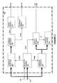
- FIG. 1 shows an exemplary internal architecture of a flash memory
- FIG. 2 is a simplified block diagram of the memory control circuit of the flash memory of FIG. 1 ;
- FIG. 3 is a high-level schematic block diagram of a flash memory device that includes the flash memory of FIG. 1 and a controller;
- FIG. 4 is a high-level block diagram of a memory system in which most of the functionality of controller of FIG. 3 is emulated by software.
- FIG. 1 shows an exemplary internal architecture for a flash memory 100 .
- the primary features include an input/output (I/O) bus 102 and control signals 104 to interface to an external controller, a memory control circuit 106 to control internal memory operations with registers for command, address and status signals.
- One or more arrays 108 of flash EEPROM cells are included, each array having its own row decoder (XDEC) 110 and column decoder (YDEC) 112 , a group of sense amplifiers and program control circuitry (SA/PROG) 114 and a data register 116 .
- the memory cells usually include one or more conductive floating gates as storage elements but other long-term electron charge storage elements may be used instead.
- the memory cell array may be operated with two levels of charge defined for each storage element to therefore store one bit of data with each element. Alternatively, more than two storage states may be defined for each storage element, in which case more than one bit of data is stored in each element.
- the external interface I/O bus 102 and control signals 104 can include the following:
- the memory have a means by which the storage subsystem controller may determine that the memory is busy performing some task.
- Such means could include a dedicated signal or a status bit in an internal memory register that is accessible while the memory is busy.
- FIG. 1 shows only one flash memory array 108 with its related components, but a multiplicity of such arrays can exist on a single flash memory chip that share a common interface and memory control circuitry but have separate XDEC 110 , YDEC 112 , SA/PROG 14 and data register 116 circuitry in order to allow parallel read and program operations.
- Data register 116 is also coupled to sense amplifier/programming circuit 114 .
- the number of elements of data register 116 coupled to each sense amplifier/programming circuit element may depend on the number of bits stored in each storage element of the memory cells, flash EEPROM cells each containing one or more floating gates as the storage elements.
- Each storage element may store a plurality of bits, such as two or four, if the memory cells are operated in a multi-state mode. Alternatively, the memory cells may be operated in a binary mode to store one bit of data per storage element.
- Row decoder 110 decodes row addresses for array 108 in order to select the physical page to be accessed.
- Row decoder 110 receives row addresses via internal row address lines 118 from memory control logic 106 .
- Column decoder 112 receives column addresses via internal column address lines 120 from memory control logic 106 .
- Rows 124 of array 108 also are referred to herein as “word lines”.
- Columns 126 of array 108 also are referred to herein as “bit lines”. For simplicity of illustration, only the first four rows 124 , the last four rows 124 , the first four columns 126 and the last four columns 126 of array 108 are shown explicitly in array 108 .
- the cells of array 108 are at the intersections of word lines 124 and bit lines 126 .
- the cells are connected in series, as in NAND flash memories, rather than in parallel as in NOR flash memories.
- Bit lines 126 are ordered, e.g. from left to right, so that the leftmost bit line 126 is assigned the ordinal number “1”, the next-to-leftmost bit line 126 is assigned the ordinal number “2”, etc.
- memory control circuit 106 in reading data from flash memory array 108 and writing data to flash memory array 108 now will be described.
- FIG. 2 is a simplified block diagram of memory control circuit 106 .
- a register enable circuit 204 has inputs coupled to an address register 206 , to a command register 202 and to a latch enable circuit 210 .
- register enable circuit 204 Upon receiving from the external controller an ALE control signal 104 that indicates that an address descriptor is to follow, register enable circuit 204 activates an enable line PADR, which causes a subsequent chunk address descriptor from the external controller on I/O bus 102 to be latched in to address register 206 .
- a latch enable circuit 210 coupled to address register 206 thereupon activates latch enable lines X and Y to latch the chunk address stored in address register 206 into appropriate row and column latches of address latches 212 .
- the chunk addresses stored in address latches 212 are then provided over appropriate lines of internal row address lines 118 to row decoder 110 and internal column address lines 120 to column decoder 112 .
- register enable circuit 204 Upon receiving from the external controller a control signal 104 that indicates that data are to follow (because the external controller wants to write the data to flash memory array 108 ), register enable circuit 204 activates an enable line PDAT that causes a chunk of data on I/O bus 102 to be latched into data register 116 .
- register enable circuit 204 Upon receiving from the external controller a CLE control signal 104 that indicates that a command is to follow, register enable circuit 204 activates an enable line PCMD, which causes a subsequent read or write command from the external controller on I/O bus 102 to be latched into command register 202 .
- a command decoder 208 thereupon reads the command stored in command register 202 .
- command decoder 208 decodes the command to activate a program line PGM.
- a program enable circuit 216 receives the program line PGM and the most significant bit from the chunk address stored in address register 206 and activates, in response thereto, program enable lines 123 provided to sense amplifier/programming circuits 114 to selectively activate their program/verify modes of operation to program the data in data register 116 into flash memory array 108 .
- command decoder 208 decodes the command to activate a sense enable circuit 214 that in turn activates sense enable line 122 provided to sense amplifier/programming circuits 114 to selectively activate their sense modes of operation to sense the threshold voltages stored in the cells at the intersections of the latched row 124 and the latched columns 126 of flash memory array 108 .
- the results of the sensing are loaded into data register 116 that then is read by the external controller.
- Each read command from the external controller causes data to be read from a single row 124 of flash memory array 108 as specified by the chunk address descriptor.
- each row value of address latches 212 is for a respective row 124 of flash memory array 108 .
- the column latches of address latches 212 are for groups of columns 126 of flash memory array 108 , with columns 126 grouped per column latch in a manner that saves the power conventionally spent on sensing soft bits.
- each group of column latches corresponds to an entire physical page on each row 124 of flash memory array 108 .
- each row 124 of cells could itself be a single physical page, or alternatively each row 124 of cells could include two, three or more physical pages.
- a command from the external controller to write data to a physical page causes sense amplifier/programming circuits 114 to program all the cells of the targeted physical page.
- a command from the external controller to read the hard bits of a physical page causes sense amplifier/programming circuits 114 to sense the hard bits of all the cells of the targeted physical page.
- a command from the external controller to read soft bits of a physical page causes sense amplifier/programming circuits 114 to read soft bits of all the cells of the targeted physical page.
- FIG. 3 is a high-level schematic block diagram of a flash memory device 300 in which flash memory 100 is controlled by an external controller 302 .
- Controller 302 is connected or connectable with a host system such as a personal computer, a digital camera, a personal digital assistant. It is the host which initiates commands, such as to store or read data to or from memory array 108 , and provides or receives such data, respectively.
- Controller 302 converts such commands into command signals that can be interpreted and executed by memory control circuit 106 .
- Controller 302 also typically contains buffer memory for the user data being written to or read from memory array 108 .
- a typical memory device 300 includes one integrated circuit chip 304 that includes controller 302 , and one or more integrated circuit chips 306 that each contains a memory 100 .
- Memory device 300 may be embedded as part of the host system, or may be included in a memory card that is removably insertable into a mating socket of host systems. Such a card may include the entire memory device, or the controller and memory array, with associated peripheral circuits, may be provided in separate cards.
- the power spent on sensing and reading hard and soft bits is composed of two portions—the first part is the power it takes to sense the memory cells into data register 116 (that is—applying reference voltages to the cells and spending power on sensing the results of the comparisons made against them), and the second part is the power it takes to transfer (“export”) the read values from data register 116 over bus 102 into external controller 302 (where the error correction decoder and other estimation functions are typically located).
- the grouping per column latch of columns 126 of flash memory array 108 that is described herein reduces the power of the first portion—the sensing of the memory cells.
- a command from external controller 302 to read soft bits of a physical page causes sense amplifier/programming circuits 114 to read soft bits of all the cells of the targeted physical page.
- sense amplifier/programming circuits 114 There are cases where we do not actually need the soft bits value for all the memory cells of a physical page, only for some of the memory cells. Nevertheless, conventionally, all the soft bit values of all the cells of a read physical page are sensed into data register 116 . But if not all those values are needed, this unnecessarily wastes power.
- some soft bits require more than one sensing operation for each cell.
- the first soft bit needs one threshold voltage comparison per cell state
- the second soft bit needs two more threshold voltage comparisons per cell state
- the third soft bit needs four more voltage comparisons per cell state, etc.
- Sensing soft bits of only some of the cells of a physical page may be required for cells in which either of the following occurs:
- the physical phenomena that cause errors in flash memory cells may be different for different states of the cells.
- a major source of errors is the drifting of the threshold voltage of memory cells with time because of leakage of electrons from the floating gates of the cells. It is typically the case that cells that are in high states (that is—states corresponding to high threshold voltages) are much more affected by drift phenomena than cells that are in low states (that is—states corresponding to low threshold voltages). This drift phenomenon is sometimes referred to as Data Retention.
- a decoder designer may therefore implement the following rule—when reading soft bits (because the decoding failed or did not converge in a designated time frame when using only hard bits), sense only soft bit values corresponding to cells that are in the upper half of the group of states (e.g. the eight highest states out of the sixteen states in a four-bit-per-cell flash memory).
- One type of decoder has the property of decoding of a code word by decoding sub-words of the full word. If one such sub-word fails to decode on its own, only then is information from other sub-words (both sub-words that did not successfully decode and sub-codes, i.e., successfully decoded sub-words) brought to help decode that sub-word.
- Soft bits may be used with such decoders after the failure of a sub-word decoding attempt and before the information from other sub-words is employed. Soft bits may be read for the failing sub-word in order to attempt to decode the failing sub-word independently of external information from other sub-words. But if only one sub-word fails and needs soft bits, there is no need to sense and transfer soft bits of all other sub-words, especially the other sub-words that decoded successfully. Therefore a designer of such a decoder may take advantage of the grouping per column latch of columns 126 of flash memory array 108 that is described herein and sense only the soft bit values of the sub-words that actually need them.
- the chunk of data read as a unit from the memory (“page” in the terminology of flash memories) is larger than the chunk of data used for the error correction process.
- a chunk of data is stored in a group of cells corresponding to a physical page of the memory (each cell storing one or more data bits), but for the purpose of decoding the data the chunk is divided into separate code words.
- a typical example is a physical page of 32K cells, with each cell storing two data bits (for a total of 64K bits), that is divided into four code words each containing 16K bits that are stored in 8K cells. Each such code word is independently decoded. Therefore it may be the case that one of the code words needs soft bits for successful decoding while the other code words do not. In such a case the storage system designer may employ the grouping per column latch of columns 126 of flash memory array 108 that is described herein and sense to data register 116 only the soft bit values corresponding to the cells storing the initially-failed code word.
- the chunk of data read as a unit from the memory (“page” in the terminology of flash memories) is larger than the chunk of data used for statistical estimation, for example of cross-coupling between cells.
- page in the terminology of flash memories
- cross-coupling between cells For sufficiently accurate estimation of cross coupling coefficients only a fraction of the page may be required. For the typical case of case “C.” above, out of 32K cells only 10K cells could be needed to estimate the cross coupling coefficients which can be then employed for all 32K cells of a word line.
- address latches 212 could include one column latch per bit-line 126 .
- Each column latch would determine whether its corresponding bit-line 126 is operative during the read sense phase and whether current is flowing through that bit-line 126 .
- controller 302 has to specify the desired state of each latch.
- a much preferable design enables and disables the power consumption of groups of many bit-lines 126 in one signal.
- each group of bit-lines 126 corresponding to one of the sub-words of example B can be controlled by a single respective column latch of address latches 212 .
- each group of bit-lines 126 corresponding to a code word of example C, or a group of example D can be controlled by a single column latch of address latches 212 .
- example A is not well supported by this preferred implementation, nevertheless some power savings could be obtained for this example as well.
- one of the hard bits of the four-bit-per-cell example is indicative if the cell belongs to the eight upper states or to the eight lower states
- This bit can be used to change the V BL (the bit line drain side voltage) to zero and thus inhibit all non-relevant bit lines.
- V BL the bit line drain side voltage
- a typical read command of a flash memory includes an address pointing to a specific byte (or word, in the less common 16-bit flash memories). The most significant bits of the address define the page being read and the least significant bytes define the byte from which sequential reading is desired. If a read command points, for example, to byte 3072 out of 4096 bytes in a page, it can be taken as an indication that controller 302 intends to read only the highest quarter of the page. Flash memory 100 may be configured so that in such case (where the read address points to offset N within the addressed page), to avoid sensing of all bit-lines with offsets less than N.
- flash memory 100 may support a command (to be issued prior to the read command) that explicitly sets two numbers—one for the lower sensed address and one for the upper sensed address. Any bit-line 126 outside the specified range then is not sensed.
- flash memory 100 may be configured to contain a “sensing control register” of several bits, each bit controlling one section of the page. For example, a 4 KB page may be divided into eight 512 bytes sectors, each controlled by one bit from an eight-bit register. Flash memory 100 , if so configured, supports a command (issued before the read command) that sets the sensing control register to any desired bit pattern, thus allowing any combination of sectors to be sensed while all other sectors are not sensed.
- the setting of the limits in method 2 and the setting of the register in method 3 may be for one read only and repeated for each page read, or may remain in effect until changed or reset to a default value.
- the time that external controller 302 spends in reading soft bits from flash memory 100 is composed of two portions—the first part is the time it takes to sense the memory cells into data register 116 (that is—the time to apply reference voltages to the cells and sense the results of the comparisons made against them), and the second part is the time it takes to transfer (“export”) the read values from data register 116 over bus 102 to external controller 302 .
- a typical flash bus cycle may be between 30 and 50 nanoseconds, in which time 8 bits are transferred (or 16 bits in the less common case of 16 bit flash devices).
- Transferring out only part of the data residing in a data register of a NAND flash memory does not require any additional circuitry or commands in the flash memory—e.g., data register 116 of flash memory 100 ) does not require any additional circuitry or commands in the flash memory—every flash memory that supports the reading of soft bits has the capability (using standard available commands) to start data transfer from any arbitrary address in the data register, transfer out any desired number of bytes sequentially from the starting address, and then re-position the transfer pointer to any desired second address in the data register, transfer sequentially any number bytes, and so on.
- a decoder designer may therefore implement the following rule—when reading soft bits (because the decoding failed when using only hard bits), read only soft bit values corresponding to cells that are in the upper half of the group of states (e.g. the eight highest states out of the sixteen states in a four-bit-per-cell flash memory).
- one type of decoder has the property of starting decoding of a code word at sub-words of the full code word. If one such sub-word fails to decode on its own, only then is information from other sub-words (both sub-words that did not successfully decode and sub-codes, i.e., successfully decoded sub-words) brought to help decode that subword. Soft bits may be used with such decoders after the failure of a sub-word decoding and before the information from other sub-words is used. Soft bits may be read for the failing sub-word in order to attempt to decode the failing sub-word locally without external information from other sub-words.
- the chunk of data read as a unit from the memory (“page” in the terminology of flash memories) is larger than the chunk of data used for the error correction process.
- a chunk of data is stored in a group of cells corresponding to a physical page of the memory (each cell storing one or more data bits), but for the purpose of decoding the data the chunk is divided into separate code words.
- a typical example is a physical page of 32K cells, with each cell storing two data bits (for a total of 64K bits), that is divided into four code words each containing 16K bits that are stored in 8K cells.
- Each such code word is independently decoded. Therefore it may be the case that one of the code words needs soft bits for successful decoding while the other code words do not.
- the storage system designer may transfer to external controller 302 only the soft bit values corresponding to the cells storing the initially-failed code word, even if the soft bits of the whole physical page are read from the memory cells to the data register at the same time and are ready to be transferred to the controller.
- FIG. 4 is a high-level block diagram of a system 400 in which most of the functionality of controller 302 is effected by software.
- System 400 includes a processor 402 and four memory devices: a RAM 404 , a boot ROM 406 , a mass storage device (hard disk) 408 and a modified flash memory device of FIG. 3 as a flash memory device 412 , all communicating via a common bus 414 .
- the difference between flash memory device 300 of FIG. 3 and flash memory device 412 is that the controller of flash memory device 412 functions only as an interface to bus 414 ; the rest of the functionality of controller 302 of FIG.
- flash memory driver code 410 that is stored in mass storage device 408 and that is executed by processor 402 to interface between user applications executed by processor 402 and flash memory device 412 , and to manage the flash memory of flash memory device 412 .
- driver code 410 emulates the functionality of controller 302 of FIG. 3 with respect to saving power and time in reading the flash cells of flash memory device 412 , as described above.
- Driver code 410 typically is included in operating system code for system 400 but also could be freestanding code.
- Mass storage device 408 is an example of a computer-readable storage medium bearing computer-readable driver code for using, as reference cells of a flash memory array, cells of the flash memory array that otherwise would not be used for any purpose.
- Other examples of such computer-readable storage media include read-only memories such as CDs bearing such code.
Landscapes
- Engineering & Computer Science (AREA)
- Computer Hardware Design (AREA)
- Read Only Memory (AREA)
Priority Applications (1)
| Application Number | Priority Date | Filing Date | Title |
|---|---|---|---|
| US12/434,652 US8433980B2 (en) | 2008-06-23 | 2009-05-03 | Fast, low-power reading of data in a flash memory |
Applications Claiming Priority (2)
| Application Number | Priority Date | Filing Date | Title |
|---|---|---|---|
| US7468408P | 2008-06-23 | 2008-06-23 | |
| US12/434,652 US8433980B2 (en) | 2008-06-23 | 2009-05-03 | Fast, low-power reading of data in a flash memory |
Publications (2)
| Publication Number | Publication Date |
|---|---|
| US20090319872A1 US20090319872A1 (en) | 2009-12-24 |
| US8433980B2 true US8433980B2 (en) | 2013-04-30 |
Family
ID=40821833
Family Applications (1)
| Application Number | Title | Priority Date | Filing Date |
|---|---|---|---|
| US12/434,652 Active 2032-02-22 US8433980B2 (en) | 2008-06-23 | 2009-05-03 | Fast, low-power reading of data in a flash memory |
Country Status (7)
| Country | Link |
|---|---|
| US (1) | US8433980B2 (de) |
| EP (1) | EP2301034B1 (de) |
| JP (1) | JP5559778B2 (de) |
| KR (1) | KR101674225B1 (de) |
| CN (1) | CN102132354B (de) |
| TW (1) | TWI489483B (de) |
| WO (1) | WO2009156876A1 (de) |
Cited By (5)
| Publication number | Priority date | Publication date | Assignee | Title |
|---|---|---|---|---|
| US20120311394A1 (en) * | 2011-05-30 | 2012-12-06 | Kabushiki Kaisha Toshiba | Memory system having multiple channels and write control method including determination of error correction channel in memory system |
| US20130117626A1 (en) * | 2011-08-17 | 2013-05-09 | Broadcom Corporation | Adaptive Ultra-Low Voltage Memory |
| US20140223261A1 (en) * | 2013-02-04 | 2014-08-07 | National Tsing Hua University | Unequal bit reliability information storage method for communication and storage systems |
| US8988946B1 (en) | 2014-07-07 | 2015-03-24 | Sandisk Technologies Inc. | Selective sense amplifier enablement |
| US9594615B2 (en) | 2014-09-30 | 2017-03-14 | Apple Inc. | Estimating flash quality using selective error emphasis |
Families Citing this family (11)
| Publication number | Priority date | Publication date | Assignee | Title |
|---|---|---|---|---|
| TWI413897B (zh) * | 2010-01-20 | 2013-11-01 | Silicon Motion Inc | 快閃記憶體之資料存取方法以及快閃記憶體裝置 |
| US8578246B2 (en) * | 2010-05-31 | 2013-11-05 | International Business Machines Corporation | Data encoding in solid-state storage devices |
| US8446786B2 (en) * | 2011-01-20 | 2013-05-21 | Micron Technology, Inc. | Outputting a particular data quantization from memory |
| US9256276B2 (en) * | 2013-09-27 | 2016-02-09 | Intel Corporation | Utilization of processor capacity at low operating frequencies |
| US9406377B2 (en) * | 2014-12-08 | 2016-08-02 | Sandisk Technologies Llc | Rewritable multibit non-volatile memory with soft decode optimization |
| US11115062B2 (en) * | 2018-03-16 | 2021-09-07 | SK Hynix Inc. | Memory system with adaptive threshold decoding and method of operating such memory system |
| US10860918B2 (en) * | 2018-08-21 | 2020-12-08 | Silicon Storage Technology, Inc. | Analog neural memory system for deep learning neural network comprising multiple vector-by-matrix multiplication arrays and shared components |
| US12009034B2 (en) | 2020-03-02 | 2024-06-11 | Micron Technology, Inc. | Classification of error rate of data retrieved from memory cells |
| WO2021191171A1 (en) * | 2020-03-25 | 2021-09-30 | F. Hoffmann-La Roche Ag | Method and system for storing measurement data detected by a sensor device and indicative of an analyte in a sample of a bodily fluid |
| US11257546B2 (en) * | 2020-05-07 | 2022-02-22 | Micron Technology, Inc. | Reading of soft bits and hard bits from memory cells |
| KR102772904B1 (ko) | 2020-06-26 | 2025-02-27 | 에스케이하이닉스 주식회사 | 메모리 장치 및 이의 동작 방법 |
Citations (8)
| Publication number | Priority date | Publication date | Assignee | Title |
|---|---|---|---|---|
| US5274599A (en) * | 1992-04-22 | 1993-12-28 | Fujitsu Limited | Flash-type nonvolatile semiconductor memory having precise erasing levels |
| US5768215A (en) | 1995-09-28 | 1998-06-16 | Samsung Electronics Co., Ltd. | Integrated circuit memory devices having interleaved read capability and methods of operating same |
| US20040060031A1 (en) | 2002-09-24 | 2004-03-25 | Sandisk Corporation | Highly compact non-volatile memory and method thereof |
| US20050135148A1 (en) * | 2003-12-22 | 2005-06-23 | Unity Semiconductor Corporation | Conductive memory array having page mode and burst mode read capability |
| US20060114730A1 (en) | 2004-12-01 | 2006-06-01 | Samsung Electronics Co., Ltd. | Nonvolatile memory devices and programming methods using subsets of columns |
| US7099179B2 (en) * | 2003-12-22 | 2006-08-29 | Unity Semiconductor Corporation | Conductive memory array having page mode and burst mode write capability |
| US20080013374A1 (en) | 2005-10-27 | 2008-01-17 | Yan Li | Method for programming of multi-state non-volatile memory using smart verify |
| US20080157169A1 (en) * | 2006-12-28 | 2008-07-03 | Yuan Jack H | Shield plates for reduced field coupling in nonvolatile memory |
Family Cites Families (6)
| Publication number | Priority date | Publication date | Assignee | Title |
|---|---|---|---|---|
| JP2002149486A (ja) * | 1991-12-19 | 2002-05-24 | Toshiba Corp | メモリシステム |
| US6621739B2 (en) * | 2002-01-18 | 2003-09-16 | Sandisk Corporation | Reducing the effects of noise in non-volatile memories through multiple reads |
| US7073103B2 (en) * | 2002-12-05 | 2006-07-04 | Sandisk Corporation | Smart verify for multi-state memories |
| US7502254B2 (en) * | 2006-04-11 | 2009-03-10 | Sandisk Il Ltd | Method for generating soft bits in flash memories |
| JP4874721B2 (ja) * | 2006-06-23 | 2012-02-15 | 株式会社東芝 | 半導体記憶装置 |
| JP4896605B2 (ja) * | 2006-07-04 | 2012-03-14 | 株式会社東芝 | 不揮発性半導体記憶システム |
-
2009
- 2009-05-03 US US12/434,652 patent/US8433980B2/en active Active
- 2009-05-05 WO PCT/IB2009/051833 patent/WO2009156876A1/en not_active Ceased
- 2009-05-05 EP EP09769686.8A patent/EP2301034B1/de not_active Not-in-force
- 2009-05-05 JP JP2011514151A patent/JP5559778B2/ja not_active Expired - Fee Related
- 2009-05-05 CN CN200980132786.XA patent/CN102132354B/zh not_active Expired - Fee Related
- 2009-05-05 KR KR1020117001408A patent/KR101674225B1/ko not_active Expired - Fee Related
- 2009-05-20 TW TW098116730A patent/TWI489483B/zh not_active IP Right Cessation
Patent Citations (9)
| Publication number | Priority date | Publication date | Assignee | Title |
|---|---|---|---|---|
| US5274599A (en) * | 1992-04-22 | 1993-12-28 | Fujitsu Limited | Flash-type nonvolatile semiconductor memory having precise erasing levels |
| US5768215A (en) | 1995-09-28 | 1998-06-16 | Samsung Electronics Co., Ltd. | Integrated circuit memory devices having interleaved read capability and methods of operating same |
| US20040060031A1 (en) | 2002-09-24 | 2004-03-25 | Sandisk Corporation | Highly compact non-volatile memory and method thereof |
| US20050135148A1 (en) * | 2003-12-22 | 2005-06-23 | Unity Semiconductor Corporation | Conductive memory array having page mode and burst mode read capability |
| US7095644B2 (en) * | 2003-12-22 | 2006-08-22 | Unity Semiconductor Corporation | Conductive memory array having page mode and burst mode read capability |
| US7099179B2 (en) * | 2003-12-22 | 2006-08-29 | Unity Semiconductor Corporation | Conductive memory array having page mode and burst mode write capability |
| US20060114730A1 (en) | 2004-12-01 | 2006-06-01 | Samsung Electronics Co., Ltd. | Nonvolatile memory devices and programming methods using subsets of columns |
| US20080013374A1 (en) | 2005-10-27 | 2008-01-17 | Yan Li | Method for programming of multi-state non-volatile memory using smart verify |
| US20080157169A1 (en) * | 2006-12-28 | 2008-07-03 | Yuan Jack H | Shield plates for reduced field coupling in nonvolatile memory |
Cited By (8)
| Publication number | Priority date | Publication date | Assignee | Title |
|---|---|---|---|---|
| US20120311394A1 (en) * | 2011-05-30 | 2012-12-06 | Kabushiki Kaisha Toshiba | Memory system having multiple channels and write control method including determination of error correction channel in memory system |
| US8589768B2 (en) * | 2011-05-30 | 2013-11-19 | Kabushiki Kaisha Toshiba | Memory system having multiple channels and write control method including determination of error correction channel in memory system |
| US20130117626A1 (en) * | 2011-08-17 | 2013-05-09 | Broadcom Corporation | Adaptive Ultra-Low Voltage Memory |
| US8700972B2 (en) * | 2011-08-17 | 2014-04-15 | Broadcom Corporation | Adaptive ultra-low voltage memory |
| US20140223261A1 (en) * | 2013-02-04 | 2014-08-07 | National Tsing Hua University | Unequal bit reliability information storage method for communication and storage systems |
| US9058880B2 (en) * | 2013-02-04 | 2015-06-16 | National Tsing Hua University | Unequal bit reliability information storage method for communication and storage systems |
| US8988946B1 (en) | 2014-07-07 | 2015-03-24 | Sandisk Technologies Inc. | Selective sense amplifier enablement |
| US9594615B2 (en) | 2014-09-30 | 2017-03-14 | Apple Inc. | Estimating flash quality using selective error emphasis |
Also Published As
| Publication number | Publication date |
|---|---|
| JP2011525681A (ja) | 2011-09-22 |
| KR20110033222A (ko) | 2011-03-30 |
| JP5559778B2 (ja) | 2014-07-23 |
| EP2301034A1 (de) | 2011-03-30 |
| US20090319872A1 (en) | 2009-12-24 |
| WO2009156876A1 (en) | 2009-12-30 |
| TWI489483B (zh) | 2015-06-21 |
| EP2301034B1 (de) | 2014-06-11 |
| CN102132354A (zh) | 2011-07-20 |
| CN102132354B (zh) | 2015-08-26 |
| TW201003666A (en) | 2010-01-16 |
| KR101674225B1 (ko) | 2016-11-08 |
Similar Documents
| Publication | Publication Date | Title |
|---|---|---|
| US8433980B2 (en) | Fast, low-power reading of data in a flash memory | |
| TWI389121B (zh) | 具有改良程式化準確性之快閃記憶體及相關方法 | |
| US20200363953A1 (en) | Flash memory system | |
| JP4533871B2 (ja) | 不揮発性メモリにおける妨害の低減方法 | |
| US8166371B2 (en) | Semiconductor memory system and signal processing system | |
| KR100348774B1 (ko) | 플래시형코어를갖는소거/기록가능롬어레이 | |
| TWI859181B (zh) | 記憶體控制器、記憶體系統及其操作方法 | |
| US11715516B2 (en) | Nonvolatile memory device including a fast read page and a storage device including the same | |
| CN102737720A (zh) | 抑制快闪存储器响应外部命令时漏电的方法与装置 | |
| US7684239B2 (en) | Flash memory device for over-sampling read and interfacing method thereof | |
| JP2009003569A (ja) | 半導体記憶装置 | |
| US9728264B2 (en) | Nonvolatile memory device, operating method thereof, and data storage device including the same | |
| KR20200120159A (ko) | 데이터 저장 장치 및 이의 동작 방법 | |
| US5748939A (en) | Memory device with a central control bus and a control access register for translating an access request into an access cycle on the central control bus | |
| US7885141B2 (en) | Non-volatile memory device and method for setting configuration information thereof | |
| US12056367B2 (en) | Memory system and operating method thereof for performing urgent fine program operation | |
| JP2005292925A (ja) | メモリコントローラ、フラッシュメモリシステム、並びに、フラッシュメモリの制御方法 | |
| JP2009003995A (ja) | 半導体記憶装置 | |
| JP2004039055A (ja) | 不揮発性半導体記憶装置 | |
| EP3783614B1 (de) | Nichtflüchtige speichervorrichtung mit einer schnellen leseseite und speichervorrichtung damit |
Legal Events
| Date | Code | Title | Description |
|---|---|---|---|
| AS | Assignment |
Owner name: SANDISK IL LTD., ISRAEL Free format text: ASSIGNMENT OF ASSIGNORS INTEREST;ASSIGNORS:ALROD, IDAN;LASSER, MENAHEM;REEL/FRAME:022628/0932 Effective date: 20090423 |
|
| STCF | Information on status: patent grant |
Free format text: PATENTED CASE |
|
| AS | Assignment |
Owner name: SANDISK TECHNOLOGIES INC., TEXAS Free format text: ASSIGNMENT OF ASSIGNORS INTEREST;ASSIGNOR:SANDISK IL LTD.;REEL/FRAME:033070/0041 Effective date: 20140610 |
|
| AS | Assignment |
Owner name: SANDISK TECHNOLOGIES LLC, TEXAS Free format text: CHANGE OF NAME;ASSIGNOR:SANDISK TECHNOLOGIES INC;REEL/FRAME:038807/0850 Effective date: 20160516 |
|
| FPAY | Fee payment |
Year of fee payment: 4 |
|
| MAFP | Maintenance fee payment |
Free format text: PAYMENT OF MAINTENANCE FEE, 8TH YEAR, LARGE ENTITY (ORIGINAL EVENT CODE: M1552); ENTITY STATUS OF PATENT OWNER: LARGE ENTITY Year of fee payment: 8 |
|
| MAFP | Maintenance fee payment |
Free format text: PAYMENT OF MAINTENANCE FEE, 12TH YEAR, LARGE ENTITY (ORIGINAL EVENT CODE: M1553); ENTITY STATUS OF PATENT OWNER: LARGE ENTITY Year of fee payment: 12 |
|
| AS | Assignment |
Owner name: SANDISK TECHNOLOGIES, INC., CALIFORNIA Free format text: ASSIGNMENT OF ASSIGNORS INTEREST;ASSIGNOR:SANDISK TECHNOLOGIES LLC;REEL/FRAME:069796/0423 Effective date: 20241227 Owner name: SANDISK TECHNOLOGIES, INC., CALIFORNIA Free format text: ASSIGNMENT OF ASSIGNOR'S INTEREST;ASSIGNOR:SANDISK TECHNOLOGIES LLC;REEL/FRAME:069796/0423 Effective date: 20241227 |
|
| AS | Assignment |
Owner name: SANDISK TECHNOLOGIES, INC., CALIFORNIA Free format text: PARTIAL RELEASE OF SECURITY INTERESTS;ASSIGNOR:JPMORGAN CHASE BANK, N.A., AS AGENT;REEL/FRAME:071382/0001 Effective date: 20250424 Owner name: JPMORGAN CHASE BANK, N.A., AS COLLATERAL AGENT, ILLINOIS Free format text: SECURITY AGREEMENT;ASSIGNOR:SANDISK TECHNOLOGIES, INC.;REEL/FRAME:071050/0001 Effective date: 20250424 |