US8242534B2 - Semiconductor device and manufacturing method thereof - Google Patents
Semiconductor device and manufacturing method thereof Download PDFInfo
- Publication number
- US8242534B2 US8242534B2 US13/018,532 US201113018532A US8242534B2 US 8242534 B2 US8242534 B2 US 8242534B2 US 201113018532 A US201113018532 A US 201113018532A US 8242534 B2 US8242534 B2 US 8242534B2
- Authority
- US
- United States
- Prior art keywords
- semiconductor region
- type semiconductor
- region
- substrate
- semiconductor
- Prior art date
- Legal status (The legal status is an assumption and is not a legal conclusion. Google has not performed a legal analysis and makes no representation as to the accuracy of the status listed.)
- Active, expires
Links
- 239000004065 semiconductor Substances 0.000 title claims abstract description 1575
- 238000004519 manufacturing process Methods 0.000 title claims description 35
- 239000000758 substrate Substances 0.000 claims abstract description 428
- 239000012535 impurity Substances 0.000 claims abstract description 271
- 238000009792 diffusion process Methods 0.000 claims description 84
- 238000005468 ion implantation Methods 0.000 claims description 42
- 238000010438 heat treatment Methods 0.000 claims description 36
- 238000000034 method Methods 0.000 claims description 36
- 230000002093 peripheral effect Effects 0.000 claims description 15
- 230000008569 process Effects 0.000 claims description 11
- 230000015572 biosynthetic process Effects 0.000 description 48
- 230000015556 catabolic process Effects 0.000 description 44
- 230000000052 comparative effect Effects 0.000 description 32
- 239000013256 coordination polymer Substances 0.000 description 31
- 230000004048 modification Effects 0.000 description 24
- 238000012986 modification Methods 0.000 description 24
- 238000009826 distribution Methods 0.000 description 23
- 230000000694 effects Effects 0.000 description 20
- 238000002161 passivation Methods 0.000 description 16
- 230000001629 suppression Effects 0.000 description 12
- 239000002344 surface layer Substances 0.000 description 12
- 238000010586 diagram Methods 0.000 description 11
- 239000010410 layer Substances 0.000 description 11
- 239000004020 conductor Substances 0.000 description 9
- 230000002708 enhancing effect Effects 0.000 description 9
- 230000002265 prevention Effects 0.000 description 9
- ZOXJGFHDIHLPTG-UHFFFAOYSA-N Boron Chemical compound [B] ZOXJGFHDIHLPTG-UHFFFAOYSA-N 0.000 description 7
- 239000006096 absorbing agent Substances 0.000 description 7
- 229910052796 boron Inorganic materials 0.000 description 7
- 239000002019 doping agent Substances 0.000 description 7
- 238000000206 photolithography Methods 0.000 description 7
- 239000011347 resin Substances 0.000 description 6
- 229920005989 resin Polymers 0.000 description 6
- VYPSYNLAJGMNEJ-UHFFFAOYSA-N Silicium dioxide Chemical compound O=[Si]=O VYPSYNLAJGMNEJ-UHFFFAOYSA-N 0.000 description 5
- 230000008878 coupling Effects 0.000 description 5
- 238000010168 coupling process Methods 0.000 description 5
- 238000005859 coupling reaction Methods 0.000 description 5
- 230000005684 electric field Effects 0.000 description 5
- 230000001965 increasing effect Effects 0.000 description 5
- 229910052814 silicon oxide Inorganic materials 0.000 description 5
- 230000008859 change Effects 0.000 description 4
- 238000005530 etching Methods 0.000 description 4
- 239000005360 phosphosilicate glass Substances 0.000 description 4
- 230000001681 protective effect Effects 0.000 description 4
- 230000002457 bidirectional effect Effects 0.000 description 3
- 239000003990 capacitor Substances 0.000 description 3
- 230000012447 hatching Effects 0.000 description 3
- 229910021421 monocrystalline silicon Inorganic materials 0.000 description 3
- 229920002120 photoresistant polymer Polymers 0.000 description 3
- 229920001721 polyimide Polymers 0.000 description 3
- 239000002151 riboflavin Substances 0.000 description 3
- 239000004149 tartrazine Substances 0.000 description 3
- 229910052782 aluminium Inorganic materials 0.000 description 2
- XAGFODPZIPBFFR-UHFFFAOYSA-N aluminium Chemical compound [Al] XAGFODPZIPBFFR-UHFFFAOYSA-N 0.000 description 2
- 230000000903 blocking effect Effects 0.000 description 2
- 239000000969 carrier Substances 0.000 description 2
- 238000005520 cutting process Methods 0.000 description 2
- 238000005516 engineering process Methods 0.000 description 2
- 239000007789 gas Substances 0.000 description 2
- 239000010931 gold Substances 0.000 description 2
- 230000006872 improvement Effects 0.000 description 2
- 239000011229 interlayer Substances 0.000 description 2
- 239000007788 liquid Substances 0.000 description 2
- 239000000463 material Substances 0.000 description 2
- 238000000059 patterning Methods 0.000 description 2
- 239000009719 polyimide resin Substances 0.000 description 2
- 238000004886 process control Methods 0.000 description 2
- 230000009467 reduction Effects 0.000 description 2
- 239000007787 solid Substances 0.000 description 2
- 239000004229 Alkannin Substances 0.000 description 1
- OAICVXFJPJFONN-UHFFFAOYSA-N Phosphorus Chemical compound [P] OAICVXFJPJFONN-UHFFFAOYSA-N 0.000 description 1
- 230000000295 complement effect Effects 0.000 description 1
- PCHJSUWPFVWCPO-UHFFFAOYSA-N gold Chemical compound [Au] PCHJSUWPFVWCPO-UHFFFAOYSA-N 0.000 description 1
- 229910052737 gold Inorganic materials 0.000 description 1
- 230000020169 heat generation Effects 0.000 description 1
- BHEPBYXIRTUNPN-UHFFFAOYSA-N hydridophosphorus(.) (triplet) Chemical compound [PH] BHEPBYXIRTUNPN-UHFFFAOYSA-N 0.000 description 1
- 238000002347 injection Methods 0.000 description 1
- 239000007924 injection Substances 0.000 description 1
- 238000005259 measurement Methods 0.000 description 1
- 229910052751 metal Inorganic materials 0.000 description 1
- 239000002184 metal Substances 0.000 description 1
- 229910052698 phosphorus Inorganic materials 0.000 description 1
- 239000011574 phosphorus Substances 0.000 description 1
- 230000002040 relaxant effect Effects 0.000 description 1
- 230000003252 repetitive effect Effects 0.000 description 1
- 238000004088 simulation Methods 0.000 description 1
- 230000007480 spreading Effects 0.000 description 1
- 238000003892 spreading Methods 0.000 description 1
Images


Classifications
-
- H—ELECTRICITY
- H01—ELECTRIC ELEMENTS
- H01L—SEMICONDUCTOR DEVICES NOT COVERED BY CLASS H10
- H01L29/00—Semiconductor devices specially adapted for rectifying, amplifying, oscillating or switching and having potential barriers; Capacitors or resistors having potential barriers, e.g. a PN-junction depletion layer or carrier concentration layer; Details of semiconductor bodies or of electrodes thereof ; Multistep manufacturing processes therefor
- H01L29/66—Types of semiconductor device ; Multistep manufacturing processes therefor
- H01L29/68—Types of semiconductor device ; Multistep manufacturing processes therefor controllable by only the electric current supplied, or only the electric potential applied, to an electrode which does not carry the current to be rectified, amplified or switched
- H01L29/70—Bipolar devices
- H01L29/74—Thyristor-type devices, e.g. having four-zone regenerative action
- H01L29/747—Bidirectional devices, e.g. triacs
-
- H—ELECTRICITY
- H01—ELECTRIC ELEMENTS
- H01L—SEMICONDUCTOR DEVICES NOT COVERED BY CLASS H10
- H01L29/00—Semiconductor devices specially adapted for rectifying, amplifying, oscillating or switching and having potential barriers; Capacitors or resistors having potential barriers, e.g. a PN-junction depletion layer or carrier concentration layer; Details of semiconductor bodies or of electrodes thereof ; Multistep manufacturing processes therefor
- H01L29/66—Types of semiconductor device ; Multistep manufacturing processes therefor
- H01L29/66007—Multistep manufacturing processes
- H01L29/66075—Multistep manufacturing processes of devices having semiconductor bodies comprising group 14 or group 13/15 materials
- H01L29/66227—Multistep manufacturing processes of devices having semiconductor bodies comprising group 14 or group 13/15 materials the devices being controllable only by the electric current supplied or the electric potential applied, to an electrode which does not carry the current to be rectified, amplified or switched, e.g. three-terminal devices
- H01L29/66363—Thyristors
- H01L29/66386—Bidirectional thyristors
Definitions
- the present invention relates to a semiconductor device and a manufacturing method thereof, and particularly to a technology effective when applied to a semiconductor device equipped with a triac and a manufacturing method thereof.
- the triac is of such a device that two complementary thyristors are coupled in antiparallel with each other to thereby allow currents to flow bidirectionally.
- the triac is used for control of alternating current and the like.
- a triac is a device used for AC control or the like. It is desired that since accurate control is required for the triac, its performance (switching performance) is enhanced as much as possible. As the characteristics whose improvements are desired in particular, there are known suppression (prevention) of a failure in commutation and an improvement in breakdown voltage.
- the failure in commutation is of the phenomenon that it occurs due to the fact that the triac is turned on unintentionally without being inputted with a gate signal, and the triac is energized at the stage where it is not to be originally energized.
- the triac therefore needs to prevent the occurrence of the commutation failure as much as possible.
- a CR absorber is coupled in parallel to the triac to prevent the failure in commutation
- an increase in the number of elements e.g., a resistor and a capacitor that configure the CR absorber
- An object of the present invention is to provide a technology capable of improving the performance of a semiconductor device.
- a semiconductor device in which a p-type semiconductor region that forms a triac is divided to be formed into a high-concentration p-type semiconductor region and a low-concentration p-type semiconductor region.
- a semiconductor device manufacturing method in which when a p-type semiconductor region for forming a triac in a semiconductor substrate is formed, the p-type semiconductor region is divided to be formed into a high-concentration p-type semiconductor region and a low-concentration p-type semiconductor region.
- the performance of a semiconductor device can be enhanced.
- FIG. 1 is a plan view of a semiconductor device showing one embodiment of the present invention
- FIG. 2 is a sectional view of the semiconductor device shown in FIG. 1 ;
- FIG. 3 is a sectional view of the semiconductor device shown in FIG. 1 ;
- FIG. 4 is a fragmentary sectional view in a manufacturing process of a semiconductor device showing one embodiment of the present invention
- FIG. 5 is a fragmentary sectional view in the manufacturing process of the semiconductor device, following FIG. 4 ;
- FIG. 6 is a fragmentary sectional view in the manufacturing process of the semiconductor device, following FIG. 5 ;
- FIG. 7 is a fragmentary sectional view in the manufacturing process of the semiconductor device, following FIG. 6 ;
- FIG. 8 is a fragmentary sectional view in the manufacturing process of the semiconductor device, following FIG. 7 ;
- FIG. 9 is a fragmentary sectional view in the manufacturing process of the semiconductor device, following FIG. 8 ;
- FIG. 10 is a fragmentary sectional view in the manufacturing process of the semiconductor device, following FIG. 9 ;
- FIG. 11 is a fragmentary sectional view in the manufacturing process of the semiconductor device, following FIG. 10 ;
- FIG. 12 is a fragmentary sectional view in the manufacturing process of the semiconductor device, following FIG. 11 ;
- FIG. 13 is a fragmentary sectional view in the manufacturing process of the semiconductor device, following FIG. 12 ;
- FIG. 14 is a diagram for explaining a triac formed in the semiconductor device shown in FIG. 1 ;
- FIG. 15 is a circuit diagram showing a used example of the triac
- FIG. 16 is an explanatory diagram showing voltage/current waveforms and a gate signal applied to the triac
- FIG. 17 is a circuit diagram showing another used example of a triac
- FIG. 18 is a sectional view of a semiconductor device according to a first comparative example
- FIG. 19 is a sectional view of a semiconductor device according to a second comparative example.
- FIG. 20 is a sectional view of a semiconductor device according to a third comparative example.
- FIG. 21 is a fragmentary sectional view of the semiconductor device showing the one embodiment of the present invention.
- FIG. 22 is a graph showing one example of an impurity concentration distribution in a depth direction of a semiconductor substrate
- FIG. 23 is a graph illustrating one example of an impurity concentration distribution in the depth direction of the semiconductor substrate.
- FIG. 24 is a sectional view of a semiconductor device showing a first modification of the one embodiment of the present invention.
- FIG. 25 is a sectional view of a semiconductor device showing a second modification of the one embodiment of the present invention.
- FIG. 26 is a sectional view of a semiconductor device showing a third modification of the one embodiment of the present invention.
- FIG. 27 is a sectional view of a semiconductor device showing a fourth modification of the one embodiment of the present invention.
- FIG. 1 is a plan view (plan layout diagram) of a semiconductor device CP 1 showing one embodiment of the present invention, i.e., a semiconductor device CP 1 having a triac (TRIAC) herein, and FIGS. 2 and 3 are respectively fragmentary sectional views thereof.
- a sectional view taken along line A 1 -A 2 of FIG. 1 corresponds approximately to FIG. 2
- a sectional view taken along line B 1 -B 2 of FIG. 1 corresponds approximately to FIG. 3 , respectively.
- FIG. 1 plan view (plan layout diagram) of a semiconductor device CP 1 showing one embodiment of the present invention, i.e., a semiconductor device CP 1 having a triac (TRIAC) herein
- FIGS. 2 and 3 are respectively fragmentary sectional views thereof.
- a sectional view taken along line A 1 -A 2 of FIG. 1 corresponds approximately to FIG. 2
- a sectional view taken along line B 1 -B 2 of FIG. 1 corresponds approximately to FIG. 3 , respectively
- a contact hole CT 1 for the electrode E 1 and a contact hole CT 2 for the electrode E 2 are shown with dotted lines to facilitate understanding thereof.
- the semiconductor device (semiconductor chip) CP 1 of the present embodiment shown in FIGS. 1 through 3 is a semiconductor device having a triac, i.e., a semiconductor device having a bidirectional thyristor, which corresponds to one in which the triac is formed in the semiconductor substrate 1 that configures the semiconductor device, i.e., one in which the bidirectional thyristor is formed in the semiconductor substrate 1 that configures the semiconductor device.
- the configuration of the semiconductor device CP 1 according to the present embodiment will be explained specifically.
- a p-type semiconductor region P 1 , a p-type semiconductor region P 1 , a p-type semiconductor region P 2 , a p-type semiconductor region P 3 , a p-type semiconductor region P 4 , a p-type semiconductor region P 5 , an n-type semiconductor region N 2 , an n-type semiconductor region N 3 , an n-type semiconductor region N 4 and an n-type semiconductor region N 5 are formed in the semiconductor substrate 1 that configure the semiconductor device CP 1 of the present embodiment.
- These p-type semiconductor regions P 1 , P 2 , P 3 , P 4 and P 5 and n-type semiconductor regions N 2 , N 3 , N 4 and N 5 are formed by introducing (diffusing more specifically) impurities (p-type impurity such as boron for the p-type semiconductor regions P 1 , P 2 , P 3 , P 4 and P 5 , and n-type impurity such as phosphorous for the n-type semiconductor regions N 2 , N 3 , N 4 and N 5 ) into the semiconductor substrate 1 .
- impurities p-type impurity such as boron for the p-type semiconductor regions P 1 , P 2 , P 3 , P 4 and P 5
- n-type impurity such as phosphorous for the n-type semiconductor regions N 2 , N 3 , N 4 and N 5
- the semiconductor substrate 1 is of a semiconductor substrate (n-type semiconductor substrate) comprised of n-type monocrystalline silicon or the like.
- a region i.e., a region in which the impurity for the p-type semiconductor regions P 1 , P 2 , P 3 , P 4 and P 5 or the n-type semiconductor regions N 2 , N 3 , N 4 and N 5 is almost undiffused
- n-type substrate region n-type semiconductor region
- the n-type substrate region N 1 is configured by part of the semiconductor substrate 1 .
- the n-type substrate region N 1 corresponds to a region (substrate region) which nearly maintains an impurity state (n-type semiconductor state) of the semiconductor substrate 1 at the stage prior to the formation of the p-type semiconductor regions P 1 , P 2 , P 3 , P 4 and P 5 and the n-type semiconductor regions N 2 , N 3 , N 4 and N 5 .
- the n-type substrate region N 1 can also be assumed to be an n-type semiconductor region.
- the n-type substrate region N 1 is interposed between the p-type semiconductor region P 2 and the p-type semiconductor region P 3 .
- a combination of the n-type substrate region N 1 , p-type semiconductor regions P 1 , P 2 , P 3 , P 4 and P 5 and n-type semiconductor regions N 2 , N 3 , N 4 and N 5 takes on the entire semiconductor substrate 1 .
- the p-type semiconductor region (eighth semiconductor region) P 1 is formed in an outer peripheral portion (outer peripheral region) of the semiconductor substrate 1 that configures the semiconductor device CP 1 of the present embodiment and reaches from the front surface of the semiconductor substrate 1 to its back surface. Therefore, a portion (region) which comes into contact with each side surface of the semiconductor substrate 1 , serves as the p-type semiconductor region P 1 .
- the n-type substrate region N 1 is demarcated (defined) by the p-type semiconductor region P 1 .
- the n-type substrate region N 1 has a periphery surrounded by the p-type semiconductor region P 1 as viewed on a planar basis. Accordingly, the side surface of the n-type substrate region N 1 is in contact with the p-type semiconductor region P 1 .
- a major surface (second major surface) lying on the formed side of back surface electrode BE is referred to as the back surface of the semiconductor substrate 1 .
- the p-type semiconductor region (first semiconductor region) P 2 , the p-type semiconductor region (second semiconductor region) P 4 , the n-type semiconductor region (third semiconductor region) N 2 , the n-type semiconductor region (fourth semiconductor region) N 3 and the n-type semiconductor region (ninth semiconductor region) N 5 are formed on the side of the front surface (first major surface) of the semiconductor substrate 1 .
- the p-type semiconductor region (seventh semiconductor region) P 3 , the p-type semiconductor region (fifth semiconductor region) P 5 and the n-type semiconductor region (sixth semiconductor region) N 4 are formed on the side of the back surface (second major surface) of the semiconductor substrate 1 .
- the p-type semiconductor region P 1 is in contact with the n-type substrate region N 1 and the p-type semiconductor regions P 3 and P 5 , but formed apart from the p-type semiconductor regions P 2 and P 4 and the n-type semiconductor regions N 2 , N 3 , N 4 and N 5 .
- the p-type semiconductor region P 2 is formed in the vicinity of the center of the semiconductor substrate 1 , which lies on the front surface side thereof.
- the p-type semiconductor region P 2 is formed within the n-type substrate region N 1 and formed so as to be surrounded with the n-type substrate region N 1 . Namely, the p-type semiconductor region P 2 is formed so as to be internally included in the n-type substrate region N 1 . If another way of viewing is taken, the side surface of the p-type semiconductor region P 2 and the bottom surface (bottom) thereof are in contact with the n-type substrate region N 1 , and the upper surface of the p-type semiconductor region P 2 is exposed at the front surface of the semiconductor substrate 1 .
- the p-type semiconductor region P 2 is formed over a depth of, for example, about 20 ⁇ m to about 50 ⁇ m from the front surface of the semiconductor substrate 1 .
- the p-type semiconductor region P 4 is formed in the vicinity of the center of the semiconductor substrate 1 , which lies on the front surface side thereof, it is formed within the p-type semiconductor region P 2 and formed so as to be lapped or surrounded with the p-type semiconductor region P 2 . Namely, the p-type semiconductor region P 4 is formed so as to be internally involved in the p-type semiconductor region P 2 . If another way of viewing is taken, the side surface of the p-type semiconductor region P 4 and the bottom surface (bottom) thereof are in contact with the p-type substrate region P 2 , and the upper surface of the p-type semiconductor region P 4 is exposed at the front surface of the semiconductor substrate 1 .
- the p-type semiconductor region P 4 is not in contact with the n-type substrate region N 1 , and the p-type semiconductor region P 2 is placed in a state of being interposed between the p-type semiconductor region P 4 and the n-type substrate region N 1 .
- the p-type semiconductor region P 4 is formed shallower than the p-type semiconductor region P 2 . Namely, the depth (distance) from the front surface of the semiconductor substrate 1 to the bottom (bottom surface) of the p-type semiconductor region P 4 is shallower (smaller) than the depth (distance) from the front surface of the semiconductor substrate 1 to the bottom (bottom surface) of the p-type semiconductor region P 2 .
- the p-type semiconductor region P 4 is formed over a depth of about 10 ⁇ m to about 30 ⁇ m from the front surface of the semiconductor substrate 1 .
- the p-type semiconductor region P 4 is higher than the p-type semiconductor region P 2 in impurity concentration (p-type impurity concentration). Therefore, the p-type semiconductor region P 4 can be assumed to be a high-concentration p-type semiconductor region or a high-concentration p-type impurity diffusion region, whereas the p-type semiconductor region P 2 can be assumed to be a low-concentration p-type semiconductor region or a low-concentration p-type impurity diffusion region. Since the p-type semiconductor region P 4 has an impurity concentration higher than that of the p-type semiconductor region P 2 , the specific resistivity (specific resistance) of the p-type semiconductor region P 4 is lower than that of the p-type semiconductor region P 2 .
- the n-type semiconductor region N 2 and the n-type semiconductor region N 3 are formed in the neighborhood of the center of the semiconductor substrate 1 on its front surface side, they are formed within the p-type semiconductor region P 4 and formed so as to be wrapped up with the p-type semiconductor region P 4 . That is, the n-type semiconductor region N 2 and the n-type semiconductor region N 3 are formed so as to be internally included in the p-type semiconductor region P 4 . If another view is taken, the side surface and bottom surface (bottom) of the n-type semiconductor region N 2 , and the side surface and bottom surface (bottom) of the n-type semiconductor region N 3 are in contact with the p-type semiconductor region P 4 .
- the upper surface of the n-type semiconductor region N 2 and the upper surface of the n-type semiconductor region N 3 are exposed at the front surface of the semiconductor substrate 1 .
- the n-type semiconductor region N 2 and the n-type semiconductor region N 3 are formed apart from each other. Therefore, the n-type semiconductor region N 2 and the n-type semiconductor region N 3 are not in contact with each other, and the p-type semiconductor region P 4 is placed in a state of being interposed between the n-type semiconductor region N 2 and the n-type semiconductor region N 3 .
- the n-type semiconductor region N 2 and the n-type semiconductor region N 3 are neither in contact with the p-type semiconductor region P 2 nor in contact with the n-type substrate region N 1 .
- the p-type semiconductor region P 4 is put in a state of being interposed between the n-type semiconductor region N 2 and the p-type semiconductor region P 2 and between the n-type semiconductor region N 3 and the p-type semiconductor region P 2 .
- the n-type semiconductor region N 2 and the n-type semiconductor region N 3 are formed shallower than the p-type semiconductor region P 4 .
- the depth (distance) from the front surface of the semiconductor substrate 1 to the bottom (bottom surface) of the n-type semiconductor region N 2 is shallower (smaller) than the depth (distance) from the front surface of the semiconductor substrate 1 to the bottom (bottom surface) of the p-type semiconductor region P 4
- the depth (distance) from the front surface of the semiconductor substrate 1 to the bottom (bottom surface) of the n-type semiconductor region N 3 is shallower (smaller) than the depth (distance) from the front surface of the semiconductor substrate 1 to the bottom (bottom surface) of the p-type semiconductor region P 4 .
- the n-type semiconductor regions N 2 and N 3 are formed over a depth of about 2 ⁇ m to about 20 ⁇ m from the front surface of the semiconductor substrate 1 .
- the n-type semiconductor region N 5 is formed on the front surface side of the semiconductor substrate 1 , it is formed in part of a surface layer portion of the n-type substrate region N 1 and formed so as to be wrapped up with the n-type substrate region N 1 or internally involved in the n-type substrate region N 1 . If another way of viewing is taken, the side surface and bottom surface (bottom) of the n-type semiconductor region N 5 are in contact with the n-type substrate region N 1 , and the upper surface of the n-type semiconductor region N 5 is exposed at the front surface of the semiconductor substrate 1 .
- the n-type semiconductor region N 5 is set higher in impurity concentration than the n-type substrate region N 1 .
- the n-type semiconductor region N 5 is set to a depth of the same degree as the n-type semiconductor regions N 2 and N 3 and formed over, for example, a depth of about 2 ⁇ m to about 20 ⁇ m from the front surface of the semiconductor substrate 1 .
- the n-type semiconductor region N 5 is formed between the p-type semiconductor region P 2 and the p-type semiconductor region P 1 .
- the n-type semiconductor region N 5 is formed apart from the p-type semiconductor regions P 1 , P 2 and P 4 and the n-type semiconductor regions N 2 and N 3 . Therefore, the n-type semiconductor region N 5 is not in contact with any of the p-type semiconductor regions P 1 , P 2 and P 4 and the n-type semiconductor regions N 2 and N 3 .
- the n-type semiconductor region N 5 is formed so as to surround the p-type semiconductor region P 2 as viewed on a planar basis, e.g., it is formed to a ring-like planar shape that surrounds the p-type semiconductor region P 2 .
- the p-type semiconductor region P 3 and the p-type semiconductor region P 5 are formed on the back surface side of the semiconductor substrate 1 .
- the p-type semiconductor region P 5 is formed in a region that comes into contact with the back surface of the semiconductor substrate 1 , and the p-type semiconductor region P 3 is formed on the side of the semiconductor substrate 1 more inner than the p-type semiconductor region P 5 .
- the p-type semiconductor region P 3 is put in a state of being interposed between the p-type semiconductor region P 5 and the n-type substrate region N 1 .
- the side surfaces of the p-type semiconductor regions P 3 and P 5 are in contact with the p-type semiconductor region P 1 .
- the p-type semiconductor region P 5 is set to an impurity concentration higher than that of the p-type semiconductor region P 1 , the p-type semiconductor region P 1 at the portion that contacts the back surface of the semiconductor substrate 1 can be replaced with the p-type semiconductor region P 5 .
- the p-type semiconductor region P 5 is higher than the p-type semiconductor region P 3 in impurity concentration (p-type impurity concentration).
- the p-type semiconductor region P 3 is lower than the p-type semiconductor region P 5 in impurity concentration (p-type impurity concentration). Therefore, the p-type semiconductor region P 5 can be assumed to be a high-concentration p-type semiconductor region or a high-concentration p-type impurity diffusion region, whereas the p-type semiconductor region P 3 can be assumed to be a low-concentration p-type semiconductor region or a low-concentration p-type impurity diffusion region.
- the p-type semiconductor region P 5 is higher than the p-type semiconductor region P 3 in impurity concentration, the specific resistivity (specific resistance) of the p-type semiconductor region P 5 is lower than that of the p-type semiconductor region P 3 .
- the p-type semiconductor region P 1 is higher than the p-type semiconductor regions P 2 and P 3 in impurity concentration (p-type impurity concentration), the p-type semiconductor region P 1 can be assumed to be a high-concentration p-type semiconductor region or a high-concentration p-type impurity diffusion region.
- the n-type semiconductor region N 4 is formed on the back surface side of the semiconductor substrate 1 , it is formed within the p-type semiconductor region P 5 and formed so as to be wrapped up with the p-type semiconductor region P 5 . Namely, the n-type semiconductor region N 4 is formed so as to be internally included in the p-type semiconductor region P 5 . If another way of viewing is taken, the side surface and bottom surface (bottom) of the n-type semiconductor region N 4 are in contact with the p-type semiconductor region P 5 , and the upper surface of the n-type semiconductor region N 4 is exposed at the back surface of the semiconductor substrate 1 .
- the n-type semiconductor region N 4 is neither in contact with the p-type semiconductor region P 3 nor in contact with the n-type substrate region N 1 .
- the p-type semiconductor region P 5 is put in a state of being interposed between the n-type semiconductor region N 4 and the p-type semiconductor region P 3 .
- the n-type semiconductor region N 4 is formed shallower than the p-type semiconductor region P 5 .
- the depth (distance) from the back surface of the semiconductor substrate 1 to the bottom (bottom surface) of the n-type semiconductor region N 4 is shallower (smaller) than the depth (distance) from the back surface of the semiconductor substrate 1 to the bottom (bottom surface) of the p-type semiconductor region P 5 .
- the n-type semiconductor region N 4 is formed over a depth of about 2 ⁇ m to about 20 ⁇ m from the back surface of the semiconductor substrate 1 .
- the back surface side of the semiconductor substrate 1 is called the upper surface and the inner side of the semiconductor substrate 1 is called the bottom surface (bottom) at the n-type semiconductor region N 4 and the p-type semiconductor region P 5 .
- the n-type semiconductor region N 2 , the n-type semiconductor region N 3 , the n-type semiconductor region N 4 and the n-type semiconductor region N 5 are higher than the n-type substrate region N 1 in impurity concentration (n-type impurity concentration). Therefore, the specific resistivity (specific resistance) of each of the n-type semiconductor regions N 2 , N 3 , N 4 and N 5 is lower than that of the n-type substrate region N 1 .
- Each of the n-type semiconductor regions N 2 , N 3 , N 4 and N 5 can be assumed to be a high-concentration n-type semiconductor region or a high-concentration n-type impurity diffusion region, and the n-type substrate region N 1 can be assumed to be a low-concentration n-type semiconductor region or a low-concentration n-type impurity diffusion region.
- the impurity concentrations (n-type impurity concentrations) of the n-type semiconductor regions N 2 , N 3 , N 4 and N 5 can be made nearly equal to each other.
- the thickness (the thickness of the semiconductor substrate 1 approximately corresponds to that of a semiconductor substrate 1 W to be describe later) of the semiconductor substrate 1 can be set to, for example, about 150 ⁇ m to about 300 ⁇ m.
- the distance (i.e., the thickness of the n-type substrate region N 1 at a portion located between the p-type semiconductor region P 2 and the p-type semiconductor region P 3 ) from the bottom (bottom surface) of the p-type semiconductor region P 2 to the upper surface of the p-type semiconductor region P 3 can be set to, for example, about 50 ⁇ m to about 260 ⁇ m.
- the bottom (bottom surface) of the p-type semiconductor region P 2 corresponds to a PN junction surface formed between the p-type semiconductor region P 2 and the n-type substrate region N 1
- the upper surface of the p-type semiconductor region P 3 corresponds to a PN junction surface formed between the p-type semiconductor region P 3 and the n-type substrate region N 1 .
- the p-type semiconductor region P 1 is in contact with the n-type substrate region N 1 and the p-type semiconductor regions P 3 and P 5 , but not in contact with other semiconductor regions (N 2 , N 3 , N 4 , N 5 , P 2 and P 4 ).
- the p-type semiconductor region P 2 is in contact with the n-type substrate region N 1 and the p-type semiconductor region P 4 , but not in contact with other semiconductor regions (N 2 , N 3 , N 4 , N 5 , P 1 , P 3 and P 5 ).
- the p-type semiconductor region P 3 is in contact with the n-type substrate region N 1 and the p-type semiconductor regions P 1 and P 5 , but not in contact with other semiconductor regions (N 2 , N 3 , N 4 , N 5 , P 2 and P 4 ).
- the p-type semiconductor region P 4 is in contact with the n-type substrate regions N 2 and N 3 and the p-type semiconductor region P 2 , but not in contact with other semiconductor regions (N 1 , N 4 , N 5 , P 1 , P 3 and P 5 ).
- the p-type semiconductor region P 5 is in contact with the n-type semiconductor region N 4 and the p-type semiconductor regions P 1 and P 3 , but not in contact with other semiconductor regions (N 1 , N 2 , N 3 , N 5 , P 2 and P 4 ).
- the n-type substrate region N 1 is in contact with the n-type semiconductor region N 5 and the p-type semiconductor regions P 1 , P 2 and P 3 , but not in contact with other semiconductor regions (N 2 , N 3 , N 4 , P 4 and P 5 ).
- the n-type semiconductor region N 2 is in contact with the p-type semiconductor region P 4 , but not in contact with other semiconductor regions (N 1 , N 3 , N 4 , N 5 , P 1 , P 2 , P 3 and P 5 ).
- the n-type semiconductor region N 3 is in contact with the p-type semiconductor region P 4 , but not in contact with other semiconductor regions (N 1 , N 2 , N 4 , N 5 , P 1 , P 2 , P 3 and P 5 ).
- the n-type semiconductor region N 4 is in contact with the p-type semiconductor region P 5 , but not in contact with other semiconductor regions (N 1 , N 2 , N 3 , N 5 , P 1 , P 2 , P 3 and P 4 ).
- the n-type semiconductor region N 5 is in contact with the n-type substrate regions N 1 , but not in contact with other semiconductor regions (N 2 , N 3 , N 4 , P 1 , P 2 , P 3 , P 4 and P 5 ).
- the semiconductor substrate 1 is configured by these semiconductor regions (N 1 , N 2 , N 3 , N 4 , N 5 , P 1 , P 2 , P 3 , P 4 and P 5 ).
- a back surface electrode (third electrode) BE is formed at the back surface (more specifically the entire back surface) of the semiconductor substrate 1 that configures the semiconductor device CP 1 of the present embodiment.
- the back surface electrode BE is in contact with both the p-type semiconductor region P 5 and the n-type semiconductor region N 4 and electrically coupled to both the p-type semiconductor region P 5 and the n-type semiconductor region N 4 .
- the back surface electrode BE is comprised of, for example, a metal film such as an Au (gold) film.
- the back surface electrode BE may be in contact with the p-type semiconductor region P 1 .
- the back surface electrode is however not in contact with other semiconductor regions (N 1 , N 2 , N 3 , N 5 , P 2 , P 3 and P 4 ).
- An insulting film (interlayer insulating film) IL is formed at the surface (major surface on the side opposite to the side at which the back surface electrode BE is formed) of the semiconductor substrate 1 that configures the semiconductor device CP 1 of the present embodiment.
- the insulating film IL is comprised of, for example, a PSG (Phospho Silicate Glass) film or the like.
- a plurality of contact holes (openings and through holes) CT are defined in the insulating film IL. Part of the major surface (front surface) of the semiconductor substrate 1 is exposed at the bottoms of the contact holes CT.
- the contact holes CT formed in the insulating film IL have contact holes CT 1 , CT 2 and CT 3 .
- the contact hole CT 1 is formed to straddle both of the n-type semiconductor region N 2 and the p-type semiconductor region P 4 . At least part of the n-type semiconductor region N 2 and part of the p-type semiconductor region P 4 are exposed at the bottom of the contact hole CT 1 .
- the contact hole CT 2 is formed to straddle both of the n-type semiconductor region N 3 and the p-type semiconductor region P 4 . At least part of the n-type semiconductor region N 3 and part of the p-type semiconductor region P 4 are exposed at the bottom of the contact hole CT 2 .
- the contact hole CT 1 and the contact hole CT 2 do not overlap on a planar basis, the region exposed at the bottom of the contact hole CT 1 , of the p-type semiconductor region P 4 , and the region thereof exposed at the bottom of the contact hole CT 2 do not overlap on a planar basis.
- the contact hole CT 3 is formed over the n-type semiconductor region N 5 . Part of the n-type semiconductor region N 5 is exposed at the bottom of the contact hole CT 3 .
- An electrode (first electrode) E 1 , an electrode (second electrode) E 2 and an electrode E 3 are formed over the surface (first major surface) of the semiconductor substrate 1 .
- the electrode E 1 is formed above the n-type semiconductor region N 2 and p-type semiconductor region P 4 exposed at the bottom of the contact hole CT 1 .
- the electrode E 2 is formed above the n-type semiconductor region N 3 and p-type semiconductor region P 4 exposed at the bottom of the contact hole CT 2 .
- the electrode E 3 is formed above the n-type semiconductor region N 5 exposed at the bottom of the contact hole CT 3 . Therefore, the electrode E 1 is electrically coupled in contact with both the n-type semiconductor region N 2 and the p-type semiconductor region P 4 .
- the electrode E 2 is electrically coupled in contact with both the n-type semiconductor region N 3 and the p-type semiconductor region P 4 .
- the electrode E 3 is electrically coupled in contact with the n-type semiconductor region N 5 .
- the electrode E 1 internally includes the contact hole CT 1
- the electrode E 2 internally includes the contact hole CT 2
- the electrode E 3 internally includes the contact hole CT 3 .
- the portions thereof located outside the contact holes CT are located over the insulating film IL as viewed on a planar basis.
- the electrode E 1 is in contact with the n-type semiconductor region N 2 and the p-type semiconductor region P 4 , but not in contact with other semiconductor regions (N 1 , N 3 , N 4 , N 5 , P 1 , P 2 , P 3 and P 5 ) and the electrodes E 2 and E 3 .
- the electrode E 2 is in contact with the n-type semiconductor region N 3 and the p-type semiconductor region P 4 , but not in contact with other semiconductor regions (N 1 , N 2 , N 4 , N 5 , P 1 , P 2 , P 3 and P 5 ) and the electrodes E 1 and E 3 .
- the electrode E 3 is in contact with the n-type semiconductor region N 5 , but not in contact with other semiconductor regions (N 1 , N 2 , N 3 , N 4 , P 1 , P 2 , P 3 , P 4 and P 5 ) and the electrodes E 1 and E 2 .
- the electrodes E 1 , E 2 and E 3 are not in contact with one another.
- the electrodes E 1 , E 2 and E 3 are formed by a conductor film of the same layer, e.g., a conductor film comprised principally of aluminum. Each of the electrodes E 1 , E 2 and E 3 is formed by forming the conductor film over the insulating film IL to fill in the contact hole CT and then patterning the conductor film.
- An insulating film PV is formed over the top layer on the front surface side of the semiconductor substrate 1 , i.e., insulating film IL as a surface protective film (passivation film).
- the electrodes E 1 , E 2 and E 3 are formed by the conductor film of the same layer, but separated from one another.
- the passivation film PV is filled in between the electrodes E 1 , E 2 and E 3 .
- the passivation film PV may serve as a resin material film (resin film) such as a polyimide film.
- a plurality of openings (contact holes, via holes) OP are formed in the passivation film PV.
- the openings OP defined in the passivation film PV have openings OP 1 and OP 2 .
- the opening OP 1 is formed above the electrode E 1 .
- Part of the electrode E 1 is exposed at the bottom of the opening OP 1 .
- the peripheral portion of the upper surface of the electrode E 1 and its side surface are covered with the passivation film PV, and the central portion of the upper surface of the electrode E 1 is exposed from the opening OP 1 .
- the opening OP 2 is formed above the electrode E 2 . Part of the electrode E 2 is exposed at the bottom of the opening OP 2 .
- the peripheral portion of the upper surface of the electrode E 2 and its side surface are covered with the passivation film PV, and the central portion of the upper surface of the electrode E 2 is exposed from the opening OP 2 .
- the electrode E 3 is covered with the passivation film PV and is not exposed.
- the electrode E 3 has a pattern shape approximately similar to the n-type semiconductor region N 5 on a planar basis.
- the electrode E 3 is configured as, for example, a ring-shaped pattern which surrounds the electrodes E 1 and E 2 . Therefore, the electrode E 3 can also be assumed to be a wiring.
- the electrode E 1 corresponding to the portion exposed from the opening OP 1 and the electrode E 2 corresponding to the portion exposed from the opening OP 2 serve bonding pads (pads or pad electrodes), and coupling members such as bonding wires can be coupled thereto. Therefore, the electrodes E 1 and E 2 can also be assumed to be terminals. Bump electrodes (protruded electrodes) can also be formed over the electrodes E 1 and E 2 exposed from the openings OP 1 and OP 2 as other forms.
- the semiconductor device of the present embodiment is obtained by cutting (dicing) a semiconductor substrate (semiconductor wafer) 1 W into a plurality of chips as will be described later. It is therefore not necessary to form the insulating films IL and PV in the peripheral portion (near-side surface region of the surface of the semiconductor substrate 1 ) of the front surface of the semiconductor substrate 1 that configures the semiconductor device CP 1 of the present embodiment. It is thus possible to facilitate the cutting (dicing) of the semiconductor substrate 1 W.
- FIGS. 4 through 13 are respectively sectional views in the manufacturing process of the semiconductor device CP 1 of the present embodiment, or a semiconductor device CP 1 having a triac herein, and show sections each corresponding to FIG. 2 .
- a semiconductor substrate (semiconductor wafer) 1 W comprised of n-type monocrystalline silicon or the like having a specific resistivity ranging from about 10 ⁇ cm to about 100 ⁇ cm, for example is first prepared.
- the front surface and back surface of the semiconductor substrate 1 W are oxidized to form a silicon oxide film (insulating film) OX.
- the major surface (first, major surface) lying on the side at which electrodes E 1 and E 2 are formed later is referred to as the front surface of the semiconductor substrate 1 W
- the major surface (second major surface) lying on the side at which a back surface electrode BE is formed later is referred to as the back surface of the semiconductor substrate 1 W.
- the silicon oxide film OX lying at an outer peripheral portion of a chip region CPR is removed from the front and back surfaces of the semiconductor substrate 1 W by using photolithography and etching methods.
- a p-type impurity such as boron (B) is diffused in the direction of inside of the semiconductor substrate 1 W from the front and back surfaces of the semiconductor substrate 1 W as a dopant to thereby form p-type semiconductor regions P 1 as shown in FIG. 5 .
- the chip region CPR corresponds to a region in which one semiconductor device (semiconductor chip) CP 1 is manufactured therefrom.
- the p-type semiconductor regions P 1 are preferably formed before other semiconductor regions (N 2 , N 3 , N 4 , N 5 , P 2 , P 3 , P 4 and P 5 ) are formed.
- the diffusion of the p-type impurity for forming the corresponding p-type semiconductor regions P 1 can be performed as follows: Solid, liquid or gas containing a p-type impurity like boron (B), for example is caused to contact the front and back surfaces of the semiconductor substrate 1 W to apply a dopant source to the front and back surfaces of the semiconductor substrate 1 W. Then the dopant (p-type impurity) is thermally diffused into the semiconductor substrate 1 W from the front and back surfaces of the semiconductor substrate 1 W.
- heat treatment at 1250 to 1300° C.
- the silicon oxide film OX functions as a mask (diffusion mask) at this time, the p-type impurity is diffused toward the inside of the semiconductor substrate 1 W from the non-formed regions of silicon oxide film OX, of the front and back surfaces of the semiconductor substrate 1 W.
- the p-type impurity is not however diffused toward the inside of the semiconductor substrate 1 W from the formed regions of silicon oxide film OX, of the front and back surfaces of the semiconductor substrate 1 W. Therefore, as shown in FIG. 5 , the p-type semiconductor regions P 1 are formed at the outer peripheral portion (outer peripheral region) of the chip region CPR.
- the p-type semiconductor region P 1 formed by diffusing the p-type impurity from the front surface side of the semiconductor substrate 1 W, and the p-type semiconductor region P 1 formed by diffusing the p-type impurity from the back surface side of the semiconductor substrate 1 W are coupled in the neighborhood of the center of the semiconductor substrate 1 W as viewed in its thickness direction. Therefore, the so-coupled p-type semiconductor region P 1 reaches from the front surface of the semiconductor substrate 1 W to the back surface thereof.
- an n-type substrate region (n-type semiconductor region) N 1 whose periphery is surrounded by the p-type semiconductor region P 1 is defined in the chip region CPR as viewed on a planar basis.
- the n-type substrate region N 1 reaches from the front surface of the semiconductor substrate 1 W to the back surface thereof.
- the n-type substrate region N 1 corresponds to a region in which after the n-type semiconductor substrate 1 W has been prepared as described above, the state of the impurity of the n-type semiconductor substrate 1 W is maintained as it is with the impurity being almost undiffused.
- the n-type substrate region N 1 can also be assumed to be an n-type semiconductor region.
- other semiconductor regions P 2 , P 3 , P 4 , P 5 , N 2 , N 3 , N 4 and N 5 ) are formed in the region (n-type substrate region N 1 ) surrounded by the p-type semiconductor region P 1 in each chip region CPR of the semiconductor substrate 1 W as will be described below.
- an impurity (p-type impurity) for the p-type semiconductor region P 2 is diffused into the semiconductor substrate 1 W from the front surface side of the semiconductor substrate 1 W to form the p-type semiconductor region P 2 on the front surface side of the semiconductor substrate 1 W.
- An impurity (p-type impurity) for the p-type semiconductor region P 3 is diffused into the semiconductor substrate 1 W from the back surface side of the semiconductor substrate 1 W to form the p-type semiconductor region P 3 on the back surface side of the semiconductor substrate 1 W.
- the p-type semiconductor regions P 2 and P 3 can be formed as follows:
- ion implantation for the p-type semiconductor region P 2 is performed from the front surface side of the semiconductor substrate 1 W to introduce an impurity (p-type impurity) for the p-type semiconductor region P 2 into the neighborhood (surface layer portion on the front surface side) of the front surface of the semiconductor substrate 1 W.
- ion implantation for the p-type semiconductor region P 3 is performed from the back surface side of the semiconductor substrate 1 W to introduce an impurity (p-type impurity) for the p-type semiconductor region P 3 into the neighborhood (surface layer portion on the back surface side) of the back surface of the semiconductor substrate 1 W.
- the p-type impurity (e.g., boron or the like) introduced by each of the ion implantation for the p-type semiconductor region P 2 and the ion implantation for the p-type semiconductor region P 3 is further diffused into the semiconductor substrate 1 W (principally diffused in the direction of thickness of the semiconductor substrate 1 W) by heat treatment to thereby form the corresponding p-type semiconductor regions P 2 and P 3 .
- heat treatment at 1250 to 1300° C. for about 25 to 50 hours can be illustrated by way of example. Since the thermal diffusion process for forming the p-type semiconductor region P 2 and the thermal diffusion process for forming the p-type semiconductor region P 3 are performed by the same heat treatment, the number of manufacturing process steps can be reduced.
- the p-type semiconductor region P 2 is formed over a depth of about 20 to 50 ⁇ m from the front surface of the semiconductor substrate 1 W.
- the p-type semiconductor region P 2 is formed to be away from the p-type semiconductor region P 1 as viewed on a planar basis and formed to be spaced apart from the end (outer peripheral portion) of the chip region CPR by about 400 to 1000 ⁇ m.
- the p-type semiconductor region P 3 is formed over a depth of about 20 to 50 ⁇ m from the back surface of the semiconductor substrate 1 W.
- the side surface of the p-type semiconductor region P 3 is placed in a state of being in contact with the p-type semiconductor region P 1 . Since the thermal diffusion process for the formation of the p-type semiconductor region P 2 and the thermal diffusion process for the formation of the p-type semiconductor region P 3 are performed by the same heat treatment, the depth from the front surface of the semiconductor substrate 1 W to the bottom surface (bottom) of the p-type semiconductor region P 2 , and the depth from the back surface of the semiconductor substrate 1 W to the bottom surface (bottom) of the p-type semiconductor region P 3 become approximately the same.
- an impurity (p-type impurity) for the p-type semiconductor region P 4 is diffused into the semiconductor substrate 1 W from the front surface side of the semiconductor substrate 1 W to form the p-type semiconductor region P 4 on the front surface side of the semiconductor substrate 1 W.
- An impurity (p-type impurity) for the p-type semiconductor region P 5 is diffused into the semiconductor substrate 1 W from the back surface side of the semiconductor substrate 1 W to form the p-type semiconductor region P 5 on the back surface side of the semiconductor substrate 1 W.
- the formed p-type semiconductor region P 4 is higher than the p-type semiconductor region P 2 in impurity concentration.
- the formed p-type semiconductor region P 5 is higher than the p-type semiconductor region P 3 in impurity concentration.
- the p-type semiconductor regions P 4 and P 5 can be formed as follows:
- ion implantation for the p-type semiconductor region P 4 is performed from the front surface side of the semiconductor substrate 1 W to introduce the impurity (p-type impurity) for the p-type semiconductor region P 4 into the neighborhood (surface layer portion on the front surface side) of the front surface of the semiconductor substrate 1 W.
- Ion implantation for the p-type semiconductor region P 5 is performed from the back surface side of the semiconductor substrate 1 W to introduce the impurity (p-type impurity) for the p-type semiconductor region P 5 into the neighborhood (surface layer portion on the back surface side) of the back surface of the semiconductor substrate 1 W.
- the p-type impurity (e.g., boron or the like) introduced by each of the ion implantation for the p-type semiconductor region P 4 and the ion implantation for the p-type semiconductor region P 5 is further diffused into the semiconductor substrate 1 W (principally diffused in the direction of thickness of the semiconductor substrate 1 W) by heat treatment to thereby form the corresponding p-type semiconductor regions P 4 and P 5 .
- heat treatment at 1100 to 1250° C. for about 10 to 30 hours can be illustrated by way of example. Since the thermal diffusion process for forming the p-type semiconductor region P 4 and the thermal diffusion process for forming the p-type semiconductor region P 5 are performed by the same heat treatment, the number of manufacturing process steps can be reduced.
- the p-type semiconductor region P 4 is formed to be internally included in the p-type semiconductor region P 2 as seen on a planar basis. Further, the p-type semiconductor region P 4 is formed shallower than the p-type semiconductor region P 2 and formed over, for example, a depth of about 10 ⁇ m to about 30 ⁇ m from the front surface of the semiconductor substrate 1 W.
- the p-type semiconductor region P 4 is formed within the p-type semiconductor region P 2 and formed to be internally included in the p-type semiconductor region P 2 even as viewed on a planar basis and in the thickness direction. Consequently, the p-type semiconductor region P 4 is not in contact with the n-type substrate region N 1 , and the p-type semiconductor region P 2 is placed in a state of being interposed between the p-type semiconductor region P 4 and the n-type substrate region N 1 .
- the p-type semiconductor region P 5 is formed shallower than the p-type semiconductor region P 3 .
- the p-type semiconductor region P 5 is formed over, for example, a depth of about 10 to 30 ⁇ m from the back surface of the semiconductor substrate 1 W. Therefore, the p-type semiconductor region P 5 is not in contact with the n-type substrate region N 1 , and the p-type semiconductor region P 3 is put in a state of being interposed between the p-type semiconductor region P 5 and the n-type substrate region N 1 .
- the side surface of the p-type semiconductor region P 5 is placed in a state of being in contact with the p-type semiconductor region P 1 .
- the thermal diffusion process for the formation of the p-type semiconductor region P 4 and the thermal diffusion process for the formation of the p-type semiconductor region P 5 are performed by the same heat treatment, the depth from the front surface of the semiconductor substrate 1 W to the bottom surface (bottom) of the p-type semiconductor region P 4 , and the depth from the back surface of the semiconductor substrate 1 W to the bottom surface (bottom) of the p-type semiconductor region P 5 become approximately the same.
- an impurity (n-type impurity) for the n-type semiconductor regions N 2 , N 3 and N 5 is diffused into the semiconductor substrate 1 W from the front surface side of the semiconductor substrate 1 W to form the n-type semiconductor regions N 2 , N 3 and N 5 on the front surface side of the semiconductor substrate 1 W.
- An impurity (n-type impurity) for the n-type semiconductor region N 4 is diffused into the semiconductor substrate 1 W from the back surface side of the semiconductor substrate 1 W to form the n-type semiconductor region N 4 on the back surface side of the semiconductor substrate 1 W.
- the formed n-type semiconductor regions N 2 , N 3 , N 4 and N 5 are higher than the n-type substrate region N 1 in impurity concentration. Specifically, the n-type semiconductor regions N 2 , N 3 , N 4 and N 5 can be formed in the following manner.
- the diffusion of the n-type impurity for forming the n-type semiconductor regions N 2 , N 3 , N 4 and N 5 can be performed in the following manner: Solid, liquid or gas containing an n-type impurity like phosphorus (P), for example is caused to contact the front and back surfaces of the semiconductor substrate 1 W to apply a dopant source to the front and back surfaces of the semiconductor substrate 1 W. Then, the dopant (n-type impurity) is thermally diffused into the semiconductor substrate 1 W from the front and back surfaces of the semiconductor substrate 1 W.
- P n-type impurity like phosphorus
- the dopant source may partly be applied to the front and back surfaces of the semiconductor substrate 1 W.
- heat treatment at 1000 to 1200° C. for about 1 to 20 hours can be illustrated by way of example.
- the thermal diffusion process for forming the n-type semiconductor region N 2 the thermal diffusion process for forming the n-type semiconductor region N 3 , the thermal diffusion process for forming the n-type semiconductor region N 4 , and the thermal diffusion process for forming the n-type semiconductor region N 5 are carried out by the same heat treatment, the number of manufacturing process steps can be reduced.
- the n-type semiconductor region N 2 and the n-type semiconductor region N 3 are formed apart from each other as viewed on a planar basis. Since the n-type semiconductor region N 2 and the n-type semiconductor region N 3 are spaced apart from each other, part of the p-type semiconductor region P 4 exists therebetween. Both of the n-type semiconductor region N 2 and the n-type semiconductor region N 3 are formed so as to be internally included in the p-type semiconductor region P 4 as seen on a planar basis.
- the n-type semiconductor region N 2 and the n-type semiconductor region N 3 are formed shallower than the p-type semiconductor region P 4 and formed over, for example, a depth of about 2 to 20 ⁇ m from the front surface of the semiconductor substrate 1 W.
- the n-type semiconductor regions N 2 and N 3 are formed within the p-type semiconductor region P 4 .
- the n-type semiconductor regions N 2 and N 3 are formed to be internally included in the p-type semiconductor region P 4 even as viewed on a planar basis and in the thickness direction.
- the n-type semiconductor region N 5 is formed in part of the surface layer portion of the n-type substrate region N 1 .
- the n-type semiconductor region N 5 is formed to a ring-like planar shape that surrounds the p-type semiconductor region P 2 , as seen on a planar basis.
- the n-type semiconductor region N 5 is formed apart from the p-type semiconductor regions P 1 and P 2 and between the p-type semiconductor region P 2 and its corresponding p-type semiconductor region P 1 .
- the n-type semiconductor region N 4 is formed to be internally included in the p-type semiconductor region P 5 as seen on a planar basis. Further, the n-type semiconductor region N 4 is formed shallower than the p-type semiconductor region P 5 and formed over, for example, a depth of about 2 ⁇ m to about 20 ⁇ m from the back surface of the semiconductor substrate 1 W. Therefore, the n-type semiconductor region N 4 is formed within the p-type semiconductor region P 5 and formed to be internally included in the p-type semiconductor region P 5 even as viewed on a planar basis and in the thickness direction.
- the respective depths from the front surface of the semiconductor substrate 1 to the respective bottom surfaces (bottoms) of the n-type semiconductor regions N 2 , N 3 and N 5 , and the depth from the back surface of the semiconductor substrate 1 to the bottom surface (bottom) of the n-type semiconductor region N 4 become approximately the same.
- an insulating film (interlayer insulating film) IL is formed over the entire major surface of the semiconductor substrate 1 W on the front surface side thereof.
- the insulating film IL can serve as, for example, a PSG (Phospho Silicate Glass) film or the like.
- a plurality of contact holes CT i.e., contact holes CT 1 , CT 2 and CT 3
- FIG. 9 steps at which the contact holes CT are formed. Part of the major surface (surface) of the semiconductor substrate 1 W is exposed at the bottoms of the contact holes CT of the insulating film IL.
- n-type semiconductor region N 2 and part of the p-type semiconductor region P 4 are exposed at the bottom of the contact hole CT 1 .
- At least part of the n-type semiconductor region N 3 and part of the p-type semiconductor region P 4 are exposed at the bottom of the contact hole CT 2 .
- Part of the n-type semiconductor region N 5 is exposed at the bottom of the contact hole CT 3 .
- electrodes E 1 , E 2 and E 3 are formed by forming a conductor film over the entire major surface of the semiconductor substrate 1 W on its front surface side and then patterning the conductor film using, for example, the photolithography method and the etching method or the like.
- the conductor film for the formation of the electrodes E 1 , E 2 and E 3 can serve as a conductor film comprised principally of aluminum, for example and can be formed by a PVD method or the like.
- the electrode E 1 is electrically coupled to the n-type semiconductor region N 2 and the p-type semiconductor region P 4 in contact therewith at the bottom of the contact hole CT 1 .
- the electrode E 2 is electrically coupled to the n-type semiconductor region N 3 and the p-type semiconductor region P 4 in contact therewith at the bottom of the contact hole CT 2 .
- the electrode E 3 is electrically coupled to the n-type semiconductor region N 5 in contact therewith at the bottom of the contact hole CT 3 .
- an insulating film PV is formed over the entire major surface of the semiconductor substrate 1 W on the front surface side thereof as a surface protective film (passivation film). That is, the passivation film PV is formed over the insulating film IL so as to cover the electrodes E 1 , E 2 and E 3 .
- the passivation film PV may serve as a resin material film (resin film) such as a polyimide resin.
- the electrodes E 1 , E 2 and E 3 are covered with the passivation film PV used as the surface protective film.
- the passivation film PV serves as a film for the top layer of the semiconductor device CP 1 and functions as a top layer protective film for protecting the semiconductor device CP 1 . Allowing the passivation film PV of the top layer to serve as a resin film (organic insulating film) like the polyimide resin or the like makes it possible to facilitate handling of the semiconductor device CP 1 with the relatively soft resin film as the top layer.
- a plurality of openings OP are formed in the passivation film PV using, for example, the photolithography method and the etching method or the like.
- FIG. 11 steps at which the openings OP are formed.
- Parts of the electrodes E 1 and E 2 are exposed at the bottoms of the openings OP of the passivation film PV. Specifically, part of the electrode E 1 is exposed from the opening OP 1 , and part of the electrode E 2 is exposed from the opening OP 2 .
- a back surface electrode BE is formed over the entire major surface of the semiconductor substrate 1 W on its back surface side.
- the back surface electrode BE can be formed by, for example, the PVD method or the like.
- the back surface electrode BE is in contact with the n-type semiconductor region N 4 and the p-type semiconductor regions P 1 and P 5 .
- the semiconductor substrate 1 W is separated into chip regions CPR by dicing.
- Each individualized chip region CPR serves as the semiconductor device (semiconductor chip) CP 1 of the present embodiment. Therefore, the semiconductor substrate 1 W corresponds to one prior to the dicing of the semiconductor substrate 1 , and the semiconductor substrate 1 corresponds to each individualized one of the semiconductor substrate 1 W.
- FIG. 14 is a diagram for describing a triac formed in the semiconductor device CP 1 of the present embodiment and shows the same section as that shown in FIG. 2 .
- the semiconductor device CP 1 of the present embodiment is of a semiconductor device formed with a triac, i.e., a semiconductor device formed with a bidirectional thyristor. Specifically, thyristors TY 1 and TY 2 are formed between the electrode E 1 and the back surface electrode BE. Incidentally, currents that can flow through the thyristors TY 1 and TY 2 are typically shown by arrows in FIG. 14 .
- the semiconductor device CP 1 has a circuit configuration in which the thyristors TY 1 and TY 2 are coupled in parallel between the electrode E 1 and the back surface electrode BE. At the thyristors TY 1 and TY 2 , however, the currents flowing between the electrode E 1 and the back surface electrode BE are opposite in direction.
- the thyristor TY 1 is formed between the back surface electrode BE and the electrode E 1 by the p-type semiconductor regions P 5 and P 3 , n-type substrate region N 1 , p-type semiconductor regions P 2 and P 4 , and n-type semiconductor region N 2 .
- the thyristor TY 1 is formed by coupling in series, p-type semiconductor regions (p-type semiconductor regions P 5 and P 3 herein), an n-type semiconductor region (n-type substrate region N 1 herein), p-type semiconductor regions (p-type semiconductor regions P 2 and P 4 herein) and an n-type semiconductor region (n-type semiconductor region N 2 herein) between the back surface electrode BE and the electrode E 1 in order from the side of the back surface electrode BE.
- the thyristor TY 2 is formed between the electrode E 1 and the back surface electrode BE by the p-type semiconductor regions P 4 and P 2 , n-type substrate region N 1 , p-type semiconductor regions P 3 and P 5 and n-type semiconductor region N 4 .
- the thyristor TY 2 is formed by coupling in series, p-type semiconductor regions (p-type semiconductor regions P 4 and P 2 herein), an n-type semiconductor region (n-type substrate region N 1 herein), p-type semiconductor regions (p-type semiconductor regions P 3 and P 5 herein) and an n-type semiconductor region (n-type semiconductor region N 4 herein) between the electrode E 1 and the back surface electrode BE in order from the electrode E 1 side.
- the back surface electrode BE side serves as an anode side thereof, and the electrode E 1 side serves as a cathode side thereof.
- the electrode E 1 side serves as an anode side thereof, and the back surface electrode BE side serves as a cathode side thereof.
- the electrode E 2 can function as a gate terminal (gate terminals of thyristors TY 1 and TY 2 ).
- the thyristor TY 1 can also serve as a thyristor in which current flows from the back surface electrode BE to the electrode E 1 via the p-type semiconductor region P 5 , p-type semiconductor region P 3 , n-type substrate region N 1 , p-type semiconductor region P 2 , p-type semiconductor region P 4 , and n-type semiconductor region N 2 .
- the thyristor TY 2 can also serve as a thyristor in which current flows from the electrode E 1 to the back surface electrode BE via the p-type semiconductor region P 4 , p-type semiconductor region P 2 , n-type substrate region N 1 , p-type semiconductor region P 3 , p-type semiconductor region P 5 and n-type semiconductor region N 4 .
- an on voltage e.g., positive potential
- an on voltage higher in potential than at the electrode E 1 is applied to the electrode E 2 corresponding to the gate terminal in a state in which the back surface electrode BE is set to a potential higher than that at the electrode E 1 (e.g., a state in which a positive potential is applied to the back surface electrode BE, and a negative potential is applied to the electrode E 1 , respectively).
- the potential of the electrode E 2 is applied to the p-type semiconductor region P 4 .
- a transistor formed by the n-type semiconductor region N 2 , p-type semiconductor regions P 4 and P 2 and n-type substrate region N 1 is first turned on.
- a transistor formed by the p-type semiconductor regions P 4 and P 2 , n-type substrate region N 1 and p-type semiconductor regions P 3 and P 5 is turned on, thereby turning on the thyristor TY 1 .
- the back surface electrode BE (anode herein) and the electrode E 1 (cathode herein) are made conductive therebetween (turned on), so that current flows from the back surface electrode BE (anode herein) to the electrode E 1 (cathode herein) via the p-type semiconductor region P 5 , p-type semiconductor region P 3 , n-type substrate region N 1 , p-type semiconductor region P 2 , p-type semiconductor region P 4 and n-type semiconductor region N 2 .
- the current flows in the direction indicated by the arrow labeled with the symbol TY 1 in FIG. 14 .
- the on state of the thyristor TY 1 is maintained even though the application of the on voltage (positive potential) to the electrode E 2 (gate terminal) is stopped, so that the passage of the current from the back surface electrode BE to the electrode E 1 (passage of current labeled with the symbol TY 1 in FIG. 14 ) is continued. It is necessary for the current passing between the back surface electrode BE and the electrode E 1 to be set to a predetermined current value or less to stop (turn off) the conduction of the thyristor TY 1 .
- the on state of the thyristor TY 1 is continued while the current passing between the back surface electrode BE and the electrode E 1 is larger than the predetermined current value, but when the current passing therebetween reaches the predetermined current value or less, the conduction of the thyristor TY 1 is stopped (turned off).
- an on voltage e.g., negative potential
- an on voltage lower in potential than at the electrode E 1 is applied to the electrode E 2 corresponding to the gate terminal in a state in which the electrode E 1 is set to a potential higher than that at the back surface electrode BE (e.g., a state in which a negative potential is applied to the back surface electrode BE, and a positive potential is applied to the electrode E 1 , respectively).
- the potential of the electrode E 2 is applied to the n-type semiconductor region N 3 .
- a transistor formed by the n-type semiconductor region N 3 , p-type semiconductor regions P 4 and P 2 and n-type substrate region N 1 is first turned on.
- the transistor formed by the p-type semiconductor regions P 4 and P 2 , n-type substrate region N 1 and p-type semiconductor regions P 3 and P 5 is turned on.
- a transistor formed by the n-type substrate region N 1 , p-type semiconductor regions P 3 and P 5 and n-type semiconductor region N 4 is turned on, thereby turning on the thyristor TY 2 .
- the electrode E 1 (anode herein) and the back surface electrode BE (cathode herein) are made conductive therebetween (turned on), so that current flows from the electrode E 1 (anode herein) to the back surface electrode BE (cathode herein) through the p-type semiconductor region P 4 , p-type semiconductor region P 2 , n-type substrate region N 1 , p-type semiconductor region P 3 , p-type semiconductor region P 5 and n-type semiconductor region N 4 .
- the current flows in the direction indicated by the arrow labeled with the symbol TY 2 in FIG. 14 .
- the on state of the thyristor TY 2 is maintained even though the application of the on voltage (negative potential) to the electrode E 2 (gate terminal) is stopped, so that the passage of the current from the electrode E 1 to the back surface electrode BE (passage of current labeled with the symbol TY 2 in FIG. 14 ) is continued. It is necessary for the current passing between the electrode E 1 and the back surface electrode BE to be set to a predetermined current value or less to stop (turn off) the conduction of the thyristor TY 2 .
- the on state of the thyristor TY 2 is continued while the current passing between the electrode E 1 and the back surface electrode BE is greater than the predetermined current value, but when the current passing therebetween reaches the predetermined current value or less, the conduction of the thyristor TY 2 is stopped (turned off).
- FIG. 15 is a circuit diagram showing a used example of the triac.
- the triac can be used as a device for controlling an alternating current. As shown in FIG. 15 , for example, the triac can be used under the coupling of a load LD and the triac in series with an ac power supply ACP. In the case of FIG. 15 , one of two main terminals (those corresponding to the electrode E 1 and the back surface electrode BE) of the triac is coupled to one terminal of the ac power supply ACP via the load LD, whereas the other thereof is coupled to the other terminal of the ac power supply ACP.
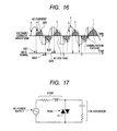
- FIG. 16 is an explanatory diagram showing voltage/current waveforms and a gate signal applied to the triac.
- An ac voltage indicated by a dotted line in FIG. 16 approximately corresponds to the waveform of an ac voltage of the ac power supply ACP.
- An ac current indicated by a dotted line in FIG. 16 shows the waveform of an ac current (virtual ac current) that can flow where no triac exists in the circuit of FIG. 15 .
- the waveforms of these ac voltage and current have a difference in phase due to the load LD or the like.
- a voltage v indicated by a solid line in FIG. 16 corresponds to a voltage applied to the triac.
- the gate signal shown in FIG. 16 corresponds to a voltage signal applied to its corresponding gate terminal (electrode E 2 herein) of the triac (semiconductor device CP 1 ).
- the triac When a gate signal GS 1 is applied to the gate terminal (one corresponding to the electrode E 2 ) of the triac in FIG. 16 , the triac (one of two thyristors corresponding to the above thyristors TY 1 and TY 2 ) is turned on so that a current i 1 shown in FIG. 16 flows. Once the current i 1 flows, the current i 1 continues to flow even if the gate signal GS 1 is turned off, but the triac is turned off at the stage where the current i 1 reaches near zero. Thereafter, the triac maintains a non-conducting state until the next gate signal GS 2 is applied to the gate terminal (one corresponding to the electrode E 2 ) of the triac, and no current flows.
- the triac (the other of the two thyristors corresponding to the above thyristors TY 1 and TY 2 ) formed in the semiconductor device CP 1 is turned on so that a current i 2 (the direction in which the current i 2 flows is opposite to the direction in which the current i 1 flows) shown in FIG. 16 flows.
- a current i 2 the direction in which the current i 2 flows is opposite to the direction in which the current i 1 flows
- the current i 2 continues to flow even if the gate signal GS 2 is turned off.
- the triac is turned off at the stage where the current i 2 reaches near zero. Thereafter, the triac maintains a non-conducting state (off state) until the next gate signal GS 3 is applied, and no current flows.
- the triac can be used as the device for controlling the ac.
- the triac is used by changing the direction in which current flowing from plus to minus directions to its opposite direction (minus to plus direction). This is referred to as “commutation”.
- FIG. 16 A failure in commutation is however occurring in FIG. 16 .
- the triac goes into an on state (turn-on) without the application of a gate signal at a spot indicated as “the failure in commutation”.
- the failure in commutation corresponds to the phenomenon that the triac is turned on unintentionally without the gate signal being input.
- This commutation failure is of a phenomenon which occurs when (di/dt)c indicative of the rate of change in current (time differential value of current) and (dv/dt)c indicative of the rate of change in voltage (time differential value of voltage) reaches a given value or more respectively.
- Controlling (dv/dt)c indicative of the rate of change in the voltage (time differential value of voltage) applied to the triac by coupling a CR absorber as in a circuit diagram shown in FIG. 17 is effective in preventing such a commutation failure.
- FIG. 17 is a circuit diagram showing another used example of the triac.
- the CR absorber is formed of a resistor and a capacitor coupled in series and is coupled in parallel to the triac. Since the CR absorber is however configured by the resistor and the capacitor, the use of the CR absorber results in an increase in the manufacturing cost and upsizing of an electronic apparatus. It is therefore desirable to make it hard to cause the commutation failure by devising the triac itself. It is also desired that the triac itself formed in the semiconductor device (semiconductor substrate) is devised because large current flows through the triac and the voltage to be applied thereto is also high, thereby achieving a triac's high breakdown voltage.
- FIG. 18 is a sectional view of the semiconductor device CP 101 according to the first comparative example and shows a section corresponding to FIG. 2 showing the present embodiment.
- the semiconductor device CP 101 according to the first comparative example shown in FIG. 18 is also of a semiconductor device formed with a triac.
- p-type semiconductor regions P 101 , a p-type semiconductor region P 102 , a p-type semiconductor region P 103 , an n-type semiconductor region N 102 , an n-type semiconductor region N 103 , an n-type semiconductor region N 104 and an n-type semiconductor region N 105 are formed in a semiconductor substrate 101 (one corresponding to the semiconductor substrate 1 of the present embodiment) that configures the semiconductor device CP 101 according to the first comparative example.
- the semiconductor substrate 101 is of a semiconductor substrate comprised of n-type monocrystalline silicon or the like.
- n-type substrate region N 101 which nearly maintains an impurity state of the semiconductor substrate 101 at the stage prior to the formation of these semiconductor regions.
- the p-type semiconductor region P 102 is formed on the front surface side of the semiconductor substrate 101 .
- the n-type semiconductor region N 102 (one corresponding to the n-type semiconductor region N 2 employed in the present embodiment) and the n-type semiconductor region N 103 (one corresponding to the n-type semiconductor region N 3 employed in the present embodiment) are formed on the front surface side of the semiconductor substrate 101 to be internally included in the p-type semiconductor region P 102 and separated from each other.
- the p-type semiconductor region P 103 is formed on the back surface side of the semiconductor substrate 101 .
- the n-type semiconductor region N 104 (one corresponding to the n-type semiconductor region N 4 employed in the present embodiment) is formed on the back surface side of the semiconductor substrate 101 to be internally included in the p-type semiconductor region P 103 .
- the p-type semiconductor region P 101 (one corresponding to the p-type semiconductor region P 1 employed in the present embodiment) is formed in an outer peripheral region of the semiconductor substrate 101 .
- the n-type substrate region N 101 (one corresponding to the n-type substrate region N 1 employed in the present embodiment) is interposed between the p-type semiconductor region P 102 and the p-type semiconductor region P 103 .
- the n-type semiconductor region N 105 (one corresponding to the n-type semiconductor region N 5 employed in the present embodiment) is formed on the front surface side of the semiconductor substrate 101 between the p-type semiconductor region P 101 and the p-type semiconductor region P 102 and is higher than the n-type substrate region N 101 in impurity concentration.
- An electrode E 101 (one corresponding to the electrode E 1 employed in the present embodiment) is formed over the front surface of the semiconductor substrate 101 to be electrically coupled in contact with the n-type semiconductor region N 102 and the p-type semiconductor region P 102 .
- An electrode E 102 (one corresponding to the electrode E 2 employed in the present embodiment) is formed over the front surface of the semiconductor substrate 101 to be electrically coupled in contact with the n-type semiconductor region N 103 and the p-type semiconductor region P 102 .
- An electrode E 103 (one corresponding to the electrode E 3 employed in the present embodiment) is formed over the front surface of the semiconductor substrate 101 to be electrically coupled in contact with the n-type semiconductor region N 105 .
- a back surface electrode BE 101 (one corresponding to the back surface electrode BE employed in the present embodiment) is formed over the back surface of the semiconductor substrate 101 to be electrically coupled in contact with the n-type semiconductor region N 104 and the p-type semiconductor regions P 101 and P 103 .
- Insulating films IL and PV are also formed over the front surface of the semiconductor substrate 101 .
- Thyristors TY 101 and TY 102 are formed in such a semiconductor device CP 101 according to the first comparative example.
- a current flows in the thyristor TY 101 from the back surface electrode BE 101 to the electrode E 101 via the p-type semiconductor region P 103 , n-type substrate region N 101 , p-type semiconductor region P 102 and n-type semiconductor region N 102 .
- a current flows in the thyristor TY 102 from the electrode E 101 to the back surface electrode BE 101 via the p-type semiconductor region P 102 , n-type substrate region N 101 , p-type semiconductor region P 103 and n-type semiconductor region N 104 .
- the electrode E 102 can function as a gate terminal.
- the breakdown voltage of the triac formed in the semiconductor device CP 101 according to the first comparative example shown in FIG. 18 is determined principally by a PN junction between the n-type substrate region N 101 and the p-type semiconductor region P 102 and a PN junction between the n-type substrate region N 101 and the p-type semiconductor region P 103 .
- the thyristor TY 101 can reliably be turned on without being so affected by the magnitude of the impurity concentration of the p-type semiconductor region P 102 .
- the failure in commutation occurs due to the fact that the thyristor TY 101 is turned on unintentionally by the injection of the electrons from the n-type semiconductor region N 102 to the p-type semiconductor region P 102 even without the application of the gate voltage.
- Increasing the impurity concentration of the p-type semiconductor region P 102 is however effective in preventing the commutation failure.
- the electrons injected into the p-type semiconductor region P 102 can be made extinctive or annihilated by being bound with holes of the p-type semiconductor region P 102 if the impurity concentration of the p-type semiconductor region P 102 is set high. It is therefore possible to prevent the thyristor TY 101 from being turned on unintentionally. Therefore, the enhancement of the impurity concentration in the p-type semiconductor region P 102 is effective in suppressing the commutation failure.
- the breakdown voltage is enhanced but the failure in commutation is easy to occur where the impurity concentration of the p-type semiconductor region P 102 is set low.
- the impurity concentration of the p-type semiconductor region P 102 is set high, the failure in commutation becomes hard to occur, but the breakdown voltage is reduced.
- the p-type semiconductor region P 103 is also similar to the above.
- the impurity concentration of the p-type semiconductor region P 103 is set low, the breakdown voltage is enhanced but the failure in commutation (that the thyristor TY 102 is turned on unintentionally) becomes easy to occur.
- the failure in commutation (that the thyristor TY 102 is turned on unintentionally) becomes hard to occur, but the breakdown voltage is reduced. It is therefore hard to allow compatibility between the enhancement of the breakdown voltage and the suppression of the failure in commutation in the semiconductor device CP 101 according to the first comparative example.
- the p-type semiconductor regions P 4 and P 2 are provide on the front surface side of the semiconductor substrate 1 .
- the p-type semiconductor region P 2 is set as the low impurity concentration
- the p-type semiconductor region P 4 is set as the high impurity concentration (impurity concentration higher than that of the p-type semiconductor region P 2 ).
- the p-type semiconductor regions P 5 and P 3 are provided on the back surface side of the semiconductor substrate 1 .
- the p-type semiconductor region P 3 is set as the low impurity concentration
- the p-type semiconductor region P 5 is set as the high impurity concentration (impurity concentration higher than that of the p-type semiconductor region P 3 ).
- the n-type semiconductor region N 2 and the n-type semiconductor region N 3 are formed on the front surface side of the semiconductor substrate 1 to be internally included in the p-type semiconductor region P 4 of the high impurity concentration and separated from each other.
- the n-type semiconductor region N 4 is formed on the back surface side of the semiconductor substrate 1 to be internally included in the p-type semiconductor region P 5 of the high impurity concentration.
- the PN junction that determines the breakdown voltage at each of the thyristors TY 1 and TY 2 in the semiconductor device CP 1 according to the present embodiment is formed by the PN junction surface between the n-type substrate region N 1 and the p-type semiconductor region P 2 of the low impurity concentration and the PN junction surface between the n-type substrate region N 1 and the p-type semiconductor region P 3 of the low impurity concentration.
- the p-type semiconductor region P 2 of the low impurity concentration is interposed between the n-type substrate region N 1 and the p-type semiconductor region P 4 of the high impurity concentration, and the p-type semiconductor region P 3 of the low impurity concentration is interposed between the n-type substrate region N 1 and the p-type semiconductor region P 5 of the high impurity concentration, the p-type semiconductor regions P 4 and P 5 of the high impurity concentrations do not form a PN junction with the n-type substrate region N 1 .
- the p-type semiconductor regions each used to form the PN junction surface for determining the breakdown voltage of the triac between each of them and the n-type substrate region N 1 are configured by the p-type semiconductor regions P 2 and P 3 of the low impurity concentrations. It is therefore possible to relax the concentration of an electric field in the vicinity of each of the PN junction surfaces (corresponding to the PN junction surface between the n-type substrate region N 1 and the p-type semiconductor region P 2 and the PN junction surface between the n-type substrate region N 1 and the p-type semiconductor region P 3 ). It is thus possible to enhance the breakdown voltage of (triac formed in) the semiconductor device CP 1 .
- the n-type semiconductor region N 2 and the n-type semiconductor region N 3 are formed so as to be internally included in the p-type semiconductor region P 4 of the high impurity concentration.
- the p-type semiconductor region P 4 of the high impurity concentration is interposed between the n-type semiconductor regions N 2 and N 3 and the p-type semiconductor region P 2 of the low impurity concentration.
- the n-type semiconductor region N 4 is formed so as to be internally included in the p-type semiconductor region P 5 of the high impurity concentration.
- the p-type semiconductor region P 5 of the high impurity concentration is interposed between the n-type semiconductor region N 4 and the p-type semiconductor region P 3 of the low impurity concentration. It is therefore possible to suppress or prevent the occurrence of the commutation failure of the triac formed in the semiconductor device CP 1 .
- the failure in commutation occurs due to the fact that the thyristor TY 1 is turned on unintentionally due to the electrons being injected from the n-type semiconductor region N 2 to the p-type semiconductor region P 4 , even without the application of the gate voltage (voltage input to the electrode E 1 ).
- the electrons injected into the p-type semiconductor region P 4 can be annihilated by being bound with the holes of the p-type semiconductor region P 4 even if such a phenomenon that the electrons are injected into the p-type semiconductor region P 4 from the n-type semiconductor region N 2 by a slight quantity occurs without the gate voltage being applied. It is therefore possible to suppress or prevent the unintentional turning on of the thyristor TY 1 without the application of the gate voltage. Accordingly, the commutation failure in the triac formed in the semiconductor device CP 1 can be suppressed or prevented.
- the failure in commutation occurs due to the fact that the thyristor TY 2 is turned on unintentionally due to the electrons being injected from the n-type semiconductor region N 4 to the p-type semiconductor region P 5 , even without the application of the gate voltage (voltage input to the electrode E 1 ).
- the quantity of holes of the p-type semiconductor region P 5 can be increased by setting high the impurity concentration of the p-type semiconductor region P 5 , the electrons injected into the p-type semiconductor region P 5 can be annihilated by being bound with the holes of the p-type semiconductor region P 5 even though such a phenomenon that the electrons are injected into the p-type semiconductor region P 5 from the n-type semiconductor region N 4 by a slight quantity occurs without the gate voltage being applied. It is therefore possible to suppress or prevent the unintentional turning on of the thyristor TY 2 without the application of the gate voltage. Accordingly, the commutation failure in the triac formed in the semiconductor device CP 1 can be suppressed or prevented.
- the p-type semiconductor region P 4 is set as the high impurity concentration in such a manner that the electrons injected from the n-type semiconductor region N 2 to the p-type semiconductor region P 4 can be annihilated with the holes of the p-type semiconductor region P 4 at other than upon the application of the gate voltage, thus making it possible to suppress or prevent the unintentional turning on of the thyristor TY 1 and thereby suppress or prevent the commutation failure in the triac (semiconductor device CP 1 ).
- the p-type semiconductor region P 5 is set as the high impurity concentration in such a manner that the electrons injected from the n-type semiconductor region N 4 to the p-type semiconductor region P 5 can be annihilated with the holes of the p-type semiconductor region P 5 at other than upon the application of the gate voltage, thus making it possible to suppress or prevent the unintentional turning on of the thyristor TY 2 and thereby suppress or prevent the commutation failure in the triac (semiconductor device CP 1 ).
- the provision of the p-type semiconductor regions P 4 and P 5 of the high impurity concentrations enables suppression of voltage fluctuations due to carriers at the commutation and increase the rate of change in current (di/dt)c corresponding to a possible limit of a failure in commutation.
- the thyristor TY 1 can reliably be turned on, even though the impurity concentration of the p-type semiconductor region P 4 is high, without being affected by, such a high impurity concentration.
- the thyristor TY 2 can reliably be turned on, even though the impurity concentration of the p-type semiconductor region P 5 is high, without being affected by such a high impurity concentration.
- the semiconductor device CP 1 makes it possible to enhance its breakdown voltage and suppress or prevent the failure in commutation. Namely, it is possible for the semiconductor device CP 1 (triac formed therein) to make compatibility between the enhancement of its breakdown voltage and the suppression (prevention) of the failure in commutation. Accordingly, the performance of the semiconductor device can be enhanced.
- the semiconductor device CP 1 (triac) itself is devised to make it hard to cause the failure in commutation in the present embodiment, the failure in commutation can be suppressed or prevented even without using the above CR absorber or the like. It is therefore possible to achieve reductions in cost and size of the electronic apparatus using the semiconductor device CP 1 (triac).
- the p-type semiconductor region (combined region of P 2 and P 4 ) located between the n-type semiconductor regions N 2 and N 3 and the n-type substrate region N 1 is formed to be divided into the p-type semiconductor region P 4 and the p-type semiconductor region P 2 in such a manner that the region adjacent to the n-type semiconductor regions N 2 and N 3 can be brought to the high impurity concentration and the region adjacent to the n-type substrate region N 1 can be brought to the low impurity concentration.
- the p-type semiconductor region P 4 is set higher than the p-type semiconductor region P 2 in impurity concentration to thereby enable the region adjacent to the n-type semiconductor regions N 2 and N 3 , of the p-type semiconductor region located between the n-type semiconductor regions N 2 and N 3 and the n-type substrate region N 1 to assume the high impurity concentration and to enable the region adjacent to the n-type substrate region N 1 , of the p-type semiconductor region to assume the low impurity concentration, thus making it possible to achieve enhancement of a breakdown voltage and suppression (prevention) of a failure in commutation.
- the p-type semiconductor region (combined region of P 3 and P 5 ) located between the n-type semiconductor region N 4 and the n-type substrate region N 1 is formed and divided into the p-type semiconductor region P 5 and the p-type semiconductor region P 3 in such a manner that the region adjacent to the n-type semiconductor region N 4 can be brought to the high impurity concentration and the region adjacent to the n-type substrate region N 1 can be brought to the low impurity concentration.
- the p-type semiconductor region P 5 is set higher than the p-type semiconductor region P 3 in impurity concentration to thereby enable the region adjacent to the n-type semiconductor region N 4 , of the p-type semiconductor region located between the n-type semiconductor region N 4 and the n-type substrate region N 1 to assume the high impurity concentration and to enable the region adjacent to the n-type substrate region N 1 to assume the low impurity concentration, thus making it possible to achieve enhancement of a breakdown voltage and suppression (prevention) of a failure in commutation.
- a depletion layer extending from the PN junction surface between the n-type substrate region N 1 and the p-type semiconductor region P 2 to the p-type semiconductor region P 2 side can be suppressed by the p-type semiconductor region P 4 of the high impurity concentration, it is possible to cause the p-type semiconductor region P 4 to function as a punchthrough stopper and prevent unintentional turning-on due to punchthrough to the n-type semiconductor region N 2 .
- a depletion layer extending from the PN junction surface between the n-type substrate region N 1 and the p-type semiconductor region P 3 to the p-type semiconductor region P 3 side can be suppressed by the p-type semiconductor region P 5 of the high impurity concentration, it is possible to cause the p-type semiconductor region P 5 to function as a punchthrough stopper and prevent unintentional turning-on due to punchthrough to the n-type semiconductor region N 4 .
- the contact resistance of the electrode E 1 can be reduced. Further, since the p-type semiconductor region with which the back surface electrode BE is brought into contact is configured as the p-type semiconductor region P 5 of the high impurity concentration, the contact resistance of the back surface electrode BE can be reduced.
- lowering the impurity concentration of the n-type substrate region N 1 i.e., increasing specific resistivity thereof
- the thickness of the semiconductor device CP 101 becomes thick because the thickness of the semiconductor substrate 101 becomes thick, thus resulting in upsizing of the semiconductor device CP 1 (increase in its thickness). Since the increase in the thickness of the semiconductor substrate 101 leads to difficulty to form the p-type semiconductor region P 101 , process control becomes difficult.
- the breakdown voltage can be enhanced by lowering the impurity concentrations of the p-type semiconductor regions P 2 and P 3 .
- the impurity concentrations of the n-type substrate regions (N 1 and N 101 ) can be made high as compared with the semiconductor device CP 101 according to the first comparative example (the n-type substrate regions can be reduced in specific resistivity), and the thicknesses of the semiconductor substrates ( 1 and 101 ) can be made thin.
- the thickness of the semiconductor device CP 1 can be thinned and the semiconductor device CP 1 can be brought into less thickness.
- An ability to make the thickness of the semiconductor substrate 1 thin leads to making it easy to form the p-type semiconductor region P 1 , so that process control becomes easy.
- the characteristic of the triac can be enhanced by reducing the specific resistivity of the n-type substrate region N 1 . Increasing the impurity concentration of the n-type substrate region N 1 makes it easy to annihilate minority carriers in the n-type substrate region N 1 . Even from this point of view, the effect of suppressing the failure in commutation can be obtained.
- FIG. 19 is a sectional view of the semiconductor device CP 201 according to the second comparative example and shows a section corresponding to FIG. 2 of the present embodiment and FIG. 18 of the first comparative example.
- the semiconductor device CP 201 according to the second comparative example shown in FIG. 19 is also effective in enhancing the breakdown voltage of the triac.
- FIG. 19 is a sectional view of the semiconductor device CP 201 according to the second comparative example and shows a section corresponding to FIG. 2 of the present embodiment and FIG. 18 of the first comparative example.
- such ring-shaped p-type semiconductor regions P 201 a and P 201 b (whose planar forms are ring-shaped) as to surround the p-type semiconductor region P 102 are formed between the p-type semiconductor region P 102 and the n-type semiconductor region N 105 .
- the ring-shaped p-type semiconductor region P 201 a is provided inwardly of the ring-shaped p-type semiconductor region P 201 b (on the side close to the p-type semiconductor region P 102 ).
- the ring-shaped p-type semiconductor region P 201 is formed to enhance a breakdown voltage as in the semiconductor device CP 201 according to the second comparative example shown in FIG. 19 , the size in the direction of the major surface of the semiconductor substrate 101 becomes large by its formation, thus resulting in an increase in the flat area of the semiconductor device CP 201 .
- the impurity concentration of the p-type semiconductor region P 2 is reduced to make it possible to enhance the breakdown voltage, a high breakdown voltage can be achieved even without forming one corresponding to the ring-shaped p-type semiconductor region P 201 . Therefore, the size in the direction of the major surface of the semiconductor substrate 1 can be suppressed, which becomes advantageous over a reduction in the area of the semiconductor device CP 1 .
- FIG. 20 is a sectional view of a semiconductor device CP 301 according to a third comparative example and shows a section corresponding to FIG. 2 of the present embodiment and FIG. 18 of the first comparative example.
- the semiconductor device CP 301 according to the third comparative example shown in FIG. 20 is of a semiconductor device formed with a triac.
- the semiconductor device CP 301 according to the third comparative example shown in FIG. 20 is different from the semiconductor device CP 101 according to the first comparative example shown in FIG. 18 in that p-type semiconductor regions P 104 and P 105 are provided.
- the p-type semiconductor region P 104 is higher than a p-type semiconductor region P 102 in impurity concentration
- the p-type semiconductor region P 105 is higher than a p-type semiconductor region P 103 in impurity concentration.
- the p-type semiconductor region P 104 is formed in a surface layer portion of the p-type semiconductor region P 102 on the front surface side of a semiconductor substrate 101 , but n-type semiconductor regions N 102 and N 103 are not internally included in the p-type semiconductor region P 104 .
- the bottoms (bottom surfaces) of the n-type semiconductor regions N 102 and N 103 are in contact with the p-type semiconductor region P 102 without contacting the p-type semiconductor region P 104 .
- the p-type semiconductor region P 105 is formed in a surface layer portion of the p-type semiconductor region P 103 on the back surface side of the semiconductor substrate 101 , but an n-type semiconductor region N 104 is not internally included in the p-type semiconductor region P 105 .
- the bottom (bottom surface) of the n-type semiconductor region N 4 is in contact with the p-type semiconductor region P 103 without contacting the p-type semiconductor region P 105 .
- the breakdown voltage is enhanced, but the failure in commutation becomes easy to occur.
- the n-type semiconductor regions N 102 and N 103 are not internally included in the p-type semiconductor region P 104 , and the bottoms (bottom surfaces) of the n-type semiconductor regions N 102 and N 103 are brought into contact with the p-type semiconductor region P 102 without contacting the p-type semiconductor region P 104 of the high impurity concentration.
- the n-type semiconductor region N 104 is not internally included in the p-type semiconductor region P 105 , and the bottom (bottom surface) of the n-type semiconductor region N 104 is not in contact with the p-type semiconductor region P 105 of the high impurity concentration but in contact with the p-type semiconductor region P 103 .
- the failure in commutation occurs due to electrons injected from the n-type semiconductor regions N 102 and N 104 to the p-type semiconductor regions P 102 and P 103 at other than upon application of a gate voltage.
- the p-type semiconductor regions P 104 and P 105 are set high in impurity concentration, it does not contribute to annihilation of the electrons injected from the n-type semiconductor regions N 102 and N 104 to the p-type semiconductor regions P 102 and P 103 . It is therefore not possible to obtain the effect of suppressing the failure in commutation.
- the n-type semiconductor regions N 2 and N 3 are internally included in the p-type semiconductor region P 4 , and the bottoms (bottom surfaces) of the n-type semiconductor regions N 2 and N 3 are not in contact with the p-type semiconductor region P 2 of the low impurity concentration but in contact with the p-type semiconductor region P 4 .
- the n-type semiconductor region N 4 is internally included in the p-type semiconductor region P 5 , and the bottom (bottom surface) of the n-type semiconductor region N 4 is not in contact with the p-type semiconductor region P 3 of the low impurity concentration but in contact with the p-type semiconductor region P 5 .
- the failure in commutation occurs due to the electrons injected from the n-type semiconductor regions N 2 and N 4 to the p-type semiconductor regions P 3 and P 5 at other than upon the application of the gate voltage. Since this can however be suppressed or prevented by setting the p-type semiconductor regions P 3 and P 5 as the high impurity concentrations respectively, such suppression or prevention is compatible with the breakdown voltage enhancement effect due to the fact that the impurity concentrations of the p-type semiconductor regions P 2 and P 4 are reduced. It is thus possible to achieve compatibility between the enhancement of the breakdown voltage and the suppression (prevention) of the failure in commutation.
- the p-type semiconductor region P 1 is preferably formed in the outer peripheral region of the semiconductor substrate 1 . Therefore, the n-type substrate region N 1 is not exposed at the side surface of the semiconductor substrate 1 that configures the semiconductor device CP 1 , and serves as the side surface configured by the p-type semiconductor region P 1 .
- the effect of preventing the exposure of the PN junction between the n-type substrate region N 1 and the p-type semiconductor region P 3 to the dicing surface (side surface of semiconductor substrate 1 ) by exposing the PN junction to the first major surface can be obtained.
- the n-type semiconductor region N 5 higher in impurity concentration than the n-type substrate region N 1 is preferably formed on the front surface side of the semiconductor substrate 1 between the p-type semiconductor region P 1 and the p-type semiconductor region P 2 (so as to surround the p-type semiconductor region P 2 ). Further, the electrode E 3 is more preferably formed above the n-type semiconductor region N 5 . It is thus possible to obtain the effect of suppressing the spread of an electric field in the surface (lateral) direction.
- the p-type semiconductor region P 2 , p-type semiconductor region P 4 , n-type semiconductor region N 2 , n-type semiconductor region N 3 and n-type semiconductor region N 5 are formed on the front surface side of the semiconductor substrate 1 .
- the p-type semiconductor region P 3 , p-type semiconductor region P 5 and n-type semiconductor region N 4 are formed on the back surface side of the semiconductor substrate 1 .
- the p-type semiconductor region P 1 is formed in the outer peripheral region of the semiconductor substrate 1 .
- These semiconductor regions are formed using the thermal diffusion (i.e., thermal diffusion process) of the impurity into the semiconductor substrate 1 W from the front or back surface of the semiconductor substrate 1 W.
- the p-type semiconductor regions P 2 and P 4 and the n-type semiconductor regions N 2 , N 3 and N 5 formed on the front surface side of the semiconductor substrate 1 are formed by thermally diffusing the impurity into the semiconductor substrate 1 ( 1 W) from the front surface side of the semiconductor substrate 1 ( 1 W), it is necessary to form the semiconductor regions whose depths are deep as viewed from the front surface of the semiconductor substrate 1 ( 1 W) ahead of the remaining semiconductor regions.
- the p-type semiconductor region P 2 is deeper than the p-type semiconductor region P 4 and the n-type semiconductor regions N 2 and N 3 in depth from the front surface of the semiconductor substrate 1 ( 1 W), and the p-type semiconductor region P 4 is deeper than the n-type semiconductor regions N 2 and N 3 in depth from the front surface thereof.
- the p-type semiconductor region P 2 is first formed (i.e., the thermal diffusion process for the formation of the p-type semiconductor region P 2 is performed). Thereafter, the p-type semiconductor region P 4 is formed (i.e., the thermal diffusion process for the formation of the p-type semiconductor region P 4 is performed). Further, the n-type semiconductor regions N 2 and N 3 are thereafter formed (i.e., the thermal diffusion process for the formation of the n-type semiconductor regions N 2 and N 3 is performed). Consequently, the p-type semiconductor region P 4 can be formed to be internally included in the p-type semiconductor region P 2 , and the n-type semiconductor regions N 2 and N 3 can be formed to be internally included in the p-type semiconductor region P 4 .
- the n-type semiconductor region N 2 and the n-type semiconductor region N 3 can also be formed in another process (another thermal diffusion process), but more preferred is if formed in the same process (same thermal diffusion process) because the number of manufacturing process steps for the semiconductor device can be reduced.
- the n-type semiconductor region N 2 and the n-type semiconductor region N 3 are formed in the same process (same thermal diffusion process) because the number of manufacturing process steps for the semiconductor device can be reduced.
- the n-type semiconductor region N 2 and the n-type semiconductor region N 3 become approximately the same in depth from the front surface of the semiconductor substrate 1 ( 1 W).
- the n-type semiconductor region N 5 is also formed in the same process as for the n-type semiconductor region N 2 and the n-type semiconductor region N 3 because the number of the manufacturing process steps for the semiconductor device can be reduced.
- the p-type semiconductor regions P 3 and P 5 and the n-type semiconductor region N 4 formed on the back surface side of the semiconductor substrate 1 are formed by thermally diffusing the impurity into the semiconductor substrate 1 ( 1 W) from the back surface side of the semiconductor substrate 1 ( 1 W), it is necessary to form the semiconductor regions whose depths are deep as viewed from the back surface of the semiconductor substrate 1 ( 1 W) ahead of the remaining semiconductor regions.
- the p-type semiconductor region P 3 is deeper than the p-type semiconductor region P 5 and the n-type semiconductor region N 4 in depth from the back surface of the semiconductor substrate 1 ( 1 W), and the p-type semiconductor region P 5 is deeper than the n-type semiconductor region N 4 in depth from the back surface of the semiconductor substrate 1 ( 1 W).
- the p-type semiconductor region P 3 is first formed (i.e., the thermal diffusion process for the formation of the p-type semiconductor region P 3 is performed). Thereafter, the p-type semiconductor region P 5 is formed (i.e., the thermal diffusion process for the formation of the p-type semiconductor region P 5 is performed). Further, the n-type semiconductor region N 4 is thereafter formed (i.e., the thermal diffusion process for the formation of the n-type semiconductor region N 4 is performed).
- the n-type semiconductor region N 4 can be formed to be internally included in the p-type semiconductor region P 5 , and the p-type semiconductor region P 3 can be interposed between the p-type substrate region P 5 and the n-type substrate region N 1 .
- the p-type semiconductor region P 2 and the p-type semiconductor region P 3 are formed in the same process (same thermal diffusion process) as shown in FIG. 6 , because the number of the manufacturing process steps for the semiconductor device can be reduced. More preferred is if the p-type semiconductor region P 4 and the p-type semiconductor region P 5 are formed in the same process (same thermal diffusion process) as shown in FIG. 7 , because the number of the manufacturing process steps for the semiconductor device can be reduced. More preferred is if the n-type semiconductor region N 2 , n-type semiconductor region N 3 , n-type semiconductor region N 4 and n-type semiconductor region N 5 are formed in the same process (same thermal diffusion process) as shown in FIG. 8 , because the number of the manufacturing process steps for the semiconductor device can be reduced.
- the triac is of a device which allows a large electric current (e.g., about a few A to about a few tens of A) to flow, there is a need to ensure its volume to some extent for the purpose of suppressing heat generation.
- the triac needs to increase the volume thereof and suppress the amount of generated heat per unit volume in such a manner that the device is not destroyed even if a surge current ranging from a few tens of A to a few hundred of A momentarily flows in the triac.
- the semiconductor substrate 1 ( 1 W) It is therefore necessary for the semiconductor substrate 1 ( 1 W) to diffuse an impurity to a fairly deep position and form the p-type semiconductor regions P 1 , P 2 , P 3 , P 4 and P 5 and the n-type semiconductor regions N 2 , N 3 , N 4 and N 5 . It is therefore difficult to form these semiconductor regions (P 1 , P 2 , P 3 , P 4 , P 5 , N 2 , N 3 , N 4 and N 5 ) by only ion implantation.
- These semiconductor regions are formed by a thermal diffusion process for diffusing the impurity into the semiconductor substrate 1 ( 1 W) by heat treatment. Further, since it is necessary to diffuse the impurity to the fairly deep position in the semiconductor substrate 1 ( 1 W) as describe above, the thermal diffusion process takes a long time at a high temperature as compared with the general manufacture of a semiconductor device.
- the p-type semiconductor region P 4 of the p-type semiconductor region P 2 and the p-type semiconductor region P 4 formed on the front surface side of the semiconductor substrate 1 ( 1 W) is formed to be shallower than the p-type semiconductor region P 2 (or be internally included in the p-type semiconductor region P 2 ) and to be higher in impurity concentration than the p-type semiconductor region P 2 . It is therefore important that the thermal diffusion process for the formation of the p-type semiconductor region P 4 is performed after the thermal diffusion process for the formation of the p-type semiconductor region P 2 has been carried out.
- the p-type semiconductor region P 2 is formed by introducing a p-type impurity into the neighborhood (surface layer portion on the front surface side) of the surface of the semiconductor substrate 1 W by ion implantation for the p-type semiconductor region P 2 and then diffusing the p-type impurity into the semiconductor substrate 1 W by the thermal diffusion process (heat treatment) for the formation of the p-type semiconductor region P 2 .
- the p-type semiconductor region P 4 is formed by introducing a p-type impurity into the neighborhood (surface layer portion on the front surface side) of the surface of the semiconductor substrate 1 W by ion implantation for the p-type semiconductor region P 4 and then diffusing the p-type impurity into the semiconductor substrate 1 W by the thermal diffusion process (heat treatment) for the formation of the p-type semiconductor region P 4 .
- the amount of dose for the ion implantation for the p-type semiconductor region P 4 conducted prior to the thermal diffusion process (heat treatment) for the formation of the p-type semiconductor region P 4 is set larger (greater) than the amount of dose for the ion implantation for the p-type semiconductor region P 2 conducted prior to the thermal diffusion process (heat treatment) for the formation of the p-type semiconductor region P 2 from the viewpoint that the p-type semiconductor region P 4 is set as the high impurity concentration and the p-type semiconductor region P 2 is set as the low impurity concentration.
- the amount of dose for the ion implantation for the p-type semiconductor region P 4 conducted prior to the thermal diffusion process (heat treatment) for the formation of the p-type semiconductor region P 4 is more preferably set to 10 to 5000 times the amount of dose for the ion implantation for the p-type semiconductor region P 2 conducted prior to the thermal diffusion process (heat treatment) for the formation of the p-type semiconductor region P 2 .
- the difference in impurity concentration between the p-type semiconductor region P 4 and the p-type semiconductor region P 2 can appropriately be ensured, and the effect of preventing the failure in commutation and the effect of enhancing the breakdown voltage can adequately be obtained.
- the above relationship between the p-type semiconductor region P 4 and the p-type semiconductor region P 2 can be applied even to the p-type semiconductor region P 5 and the p-type semiconductor region P 3 from a similar viewpoint.
- the p-type semiconductor region P 3 is formed by introducing a p-type impurity into the neighborhood (surface layer portion on the back surface side) of the back surface of the semiconductor substrate 1 W by ion implantation for the p-type semiconductor region P 3 and then diffusing the p-type impurity into the semiconductor substrate 1 W by the thermal diffusion process (heat treatment) for the formation of the p-type semiconductor region P 3 .
- the p-type semiconductor region P 5 is formed by introducing a p-type impurity into the neighborhood (surface layer portion on the back surface side) of the back surface of the semiconductor substrate 1 W by ion implantation for the p-type semiconductor region P 5 and then diffusing the p-type impurity into the semiconductor substrate 1 W by the thermal diffusion process (heat treatment) for the formation of the p-type semiconductor region P 5 .
- the amount of dose for the ion implantation for the p-type semiconductor region P 5 conducted prior to the thermal diffusion process (heat treatment) for the formation of the p-type semiconductor region P 5 is set larger (greater) than the amount of dose for the ion implantation for the p-type semiconductor region P 3 conducted prior to the thermal diffusion process (heat treatment) for the formation of the p-type semiconductor region P 3 , and is set to 10 to 5000 times the amount of dose for the ion implantation for the p-type semiconductor region P 3 .
- the difference in impurity concentration between the p-type semiconductor region P 5 and the p-type semiconductor region P 3 can appropriately be ensured, and the effect of preventing the failure in commutation and the effect of enhancing the breakdown voltage can adequately be obtained.
- the thermal diffusion process (thermal diffusion process conducted to obtain the structure of FIG. 6 from the state, of FIG. 5 ) for the formation of the p-type semiconductor region P 2 is preferably performed for a longer period of time than the time for the thermal diffusion process (thermal diffusion process conducted to obtain the structure of FIG. 7 from the state of FIG. 6 ) for the formation of the p-type semiconductor region P 4 (i.e., the time for heat treatment is preferably made longer than the time therefor) in such a manner that the difference in depth (depth as viewed from the front surface of the semiconductor substrate 1 ) between the p-type semiconductor region P 4 and the p-type semiconductor region P 2 can sufficiently be ensured.
- the thermal diffusion process (thermal diffusion process conducted to obtain the structure of FIG. 6 from the state of FIG. 5 ) for the formation of the p-type semiconductor region P 3 is preferably performed for a longer period of time than the time for the thermal diffusion process (thermal diffusion process conducted to obtain the structure of FIG. 7 from the state of FIG. 6 ) for the formation of the p-type semiconductor region P 5 (i.e., the time for heat treatment is preferably made longer than the time therefor) in such a manner that the difference in depth (depth as viewed from the front surface of the semiconductor substrate 1 ) between the p-type semiconductor region P 5 and the p-type semiconductor region P 3 can sufficiently be ensured.
- FIG. 21 is a fragmentary sectional view (partly enlarged sectional view) of the semiconductor device CP 1 according to the present embodiment and shows, in enlarged form, parts of the n-type semiconductor regions N 2 and N 3 and p-type semiconductor regions P 2 and P 4 , and the n-type substrate region N 1 lying therearound at the section corresponding to FIG. 2 .
- FIGS. 22 and 23 are respectively graphs (explanatory diagrams) showing one example illustrative of impurity concentration distributions in the direction of the depth of the semiconductor substrate 1 that configures the semiconductor device CP 1 . The horizontal axis of the graph shown in each of FIGS.
- FIGS. 22 and 23 corresponds to the depth from the front surface of the semiconductor substrate 1
- the vertical axis of the graph shown in each of FIGS. 22 and 23 corresponds to the impurity concentration.
- FIGS. 22 and 23 are shown in semilogarithmic graph form. The vertical axis corresponds to a logarithmic scale. Since FIGS. 22 and 23 show one example illustrative of the concentration distributions, the representation of actual numerical values is omitted.
- An impurity concentration distribution at a position taken along line C 1 -C 2 in FIG. 21 is shown in the graph of FIG. 22 by a solid line.
- An impurity concentration distribution at a position taken along line C 3 -C 4 in FIG. 21 is shown in the graph of FIG. 23 by a solid line.
- An impurity concentration distribution at a position taken along line C 5 -C 6 in FIG. 21 is shown in the graph of FIG. 23 by a dotted line.
- the dotted line impurity concentration distribution at the position taken along line C 5 -C 6
- the solid line impurity concentration distribution at the position taken along line C 3 -C 4
- the impurity concentration distributions can be measured by, for example, SRP (Spreading Resistance Profiler) measurements.
- the respective impurity concentrations of the n-type semiconductor region N 2 , p-type semiconductor region P 2 and p-type semiconductor region P 4 can also be assumed to be constant within the respective semiconductor regions (in this case, the graphs of FIGS. 22 and 23 are made stepwise). As shown in FIGS. 22 and 23 , however, the n-type semiconductor region N 2 , the p-type semiconductor region P 2 and the p-type semiconductor region P 4 may respectively have such impurity concentration distributions that as the depth from the front surface of the semiconductor substrate 1 becomes deep, the impurity concentrations are reduced.
- the respective semiconductor regions (N 2 , N 3 , N 4 , N 5 , P 1 , P 2 , P 3 , P 4 and P 5 ) are formed using the thermal diffusion.
- the highest impurity concentration is reached in the vicinity of the front surface of the semiconductor substrate 1 .
- the depth from the front surface of the semiconductor substrate 1 becomes deep, it is apt to reach such a concentration distribution that the impurity concentration is lowered.
- the p-type semiconductor region P 2 and the p-type semiconductor region P 4 are formed in a divided fashion in manufacture, and the thermal diffusion process (heat treatment) for the formation of the p-type semiconductor region P 4 is performed after the thermal diffusion process (heat treatment) for the formation of the p-type semiconductor region P 2 .
- the amount of dose for the ion implantation for the p-type semiconductor region P 4 conducted prior to the thermal diffusion process (heat treatment) for the formation of the p-type semiconductor region P 4 is made larger (greater) than the amount of dose for the ion implantation for the p-type semiconductor region P 2 conducted prior to the thermal diffusion process (heat treatment) for the formation of the p-type semiconductor region P 2 .
- the difference in impurity concentration between the p-type semiconductor region P 2 and the p-type semiconductor region P 4 can be made larger in the present embodiment.
- the impurity concentration of the p-type semiconductor region (P 4 ) adjacent to the n-type semiconductor regions N 2 and N 3 can be enhanced while the impurity concentration of the p-type semiconductor region (P 2 ) adjacent to the n-type substrate region N 1 is being reduced low.
- the impurity concentration of the p-type semiconductor region (P 2 ) adjacent to the n-type substrate region N 1 can be lowered while the impurity concentration of the p-type semiconductor region (P 4 ) adjacent to the n-type semiconductor regions N 2 and N 3 remains held high. This can be said even where the concentration distribution that the impurity concentration is lowered as the depth from the front surface of the semiconductor substrate 1 becomes deep is reached as shown in FIGS. 22 and 23 . The effect of enhancing a breakdown voltage can therefore be enhanced.
- Such a relationship of the impurity concentration distribution between the p-type semiconductor region P 2 and the p-type semiconductor region P 4 can be mentioned even with respect to the relationship of impurity concentration distribution between the p-type semiconductor region P 3 and the p-type semiconductor region P 5 . Since the p-type semiconductor regions P 2 and P 4 are however formed on the front surface side of the semiconductor substrate 1 , such a concentration distribution that the impurity concentration is lowered as the depth from the front surface of the semiconductor substrate 1 becomes deep can be reached. On the other hand, since the p-type semiconductor regions P 3 and P 5 are formed on the back surface side of the semiconductor substrate 1 , such a concentration distribution that the impurity concentration is lowered as the depth from the back surface of the semiconductor substrate 1 becomes deep can be reached.
- the respective impurity concentrations of the semiconductor regions (N 2 , N 3 , N 4 , N 5 , P 1 , P 2 , P 3 , P 4 and P 5 ) that configure the semiconductor substrate 1 are allowed to have such impurity concentration distributions that the impurity concentrations are lowered as the depth from the major surface (front or back surface) of the semiconductor substrate 1 becomes deep, as in the concentration distributions shown in FIGS. 22 and 23 as well as to be constant within the respective semiconductor regions.
- the p-type semiconductor region P 2 of the low impurity concentration and the p-type semiconductor region P 4 of the high impurity concentration are dared to be formed in the divided fashion in the manufacturing process. Therefore, a surface concentration (impurity concentration at the surface of the p-type semiconductor region P 4 ) ⁇ 1 of the p-type semiconductor region P 4 is higher than a surface concentration (impurity concentration at the surface of the p-type semiconductor region P 2 ) ⁇ 2 of the p-type semiconductor region P 2 .
- the surface concentration ⁇ 1 of the p-type semiconductor region P 4 ranges from over 50 times to under 5000 times the surface concentration ⁇ 2 of the p-type semiconductor region P 2 (i.e., ⁇ 2 ⁇ 50 ⁇ 1 ⁇ 2 ⁇ 5000).
- the surface concentration ⁇ 1 of the p-type semiconductor region P 4 and the surface concentration ⁇ 2 of the p-type semiconductor region P 2 are shown in the graph of FIG. 23 .
- the surface concentration ⁇ 1 of the p-type semiconductor region P 4 corresponds to the impurity concentration of the p-type semiconductor region P 4 at the surface (first major surface) of the semiconductor substrate 1 .
- the surface concentration ⁇ 1 of the p-type semiconductor region P 4 corresponds to an impurity concentration in a region (region in which the depth from the front surface of the semiconductor substrate 1 falls within a range from approximately 0 to 2 ⁇ m) lying in the neighborhood of the front surface of the semiconductor substrate 1 , of the p-type semiconductor region P 4 .
- the impurity concentration of a region PS 1 shown in FIG. 21 can be assumed to be the surface concentration ⁇ 1 of the p-type semiconductor region P 4 .
- the surface concentration ⁇ 2 of the p-type semiconductor region P 2 corresponds to the impurity concentration of the p-type semiconductor region P 2 at the surface (first major surface) of the semiconductor substrate 1 .
- the surface concentration ⁇ 2 of the p-type semiconductor region P 2 corresponds to an impurity concentration in a region (region in which the depth from the front surface of the semiconductor substrate 1 falls within a range from approximately 0 to 2 ⁇ m) lying in the neighborhood of the front surface of the semiconductor substrate 1 , of the p-type semiconductor region P 2 .
- the impurity concentration of a region PS 2 shown in FIG. 21 can be assumed to be the surface concentration ⁇ 2 of the p-type semiconductor region P 2 .
- the surface concentration (impurity concentration at the surface of the p-type semiconductor region P 2 ) ⁇ 2 of the p-type semiconductor region P 2 is higher than an impurity concentration ⁇ 3 of the n-type substrate region N 1 .
- the surface concentration ⁇ 2 of the p-type semiconductor region P 2 ranges from over 5 times to under 500 times the impurity concentration ⁇ 3 of the n-type substrate region N 1 (i.e., ⁇ 3 ⁇ 5 ⁇ 2 ⁇ 3 ⁇ 500).
- the impurity concentration ⁇ 3 of the n-type substrate region N 1 is shown in the graph of FIG. 23 .
- the impurity concentration ⁇ 3 of the n-type substrate region N 1 corresponds to the impurity concentration of a region of the n-type substrate region N 1 , which is spaced apart from the p-type semiconductor regions P 1 , P 2 , P 3 , P 4 and P 5 and the n-type semiconductor regions N 2 , N 3 , N 4 and N 5 by some degree and becomes approximately constant in impurity concentration.
- the impurity concentration ⁇ 3 of the n-type substrate region N 1 is approximately the same as the impurity concentration of the semiconductor substrate 1 W at the stage prior to the formation of the p-type semiconductor regions P 1 , P 2 , P 3 , P 4 , P 5 and the n-type semiconductor regions N 2 , N 3 , N 4 and N 5 .
- an impurity concentration of a p-type semiconductor region in which p-type and n-type impurities exist in mixed form it means an effective p-type impurity concentration obtained by subtracting the concentration of the n-type impurity actually contained therein from the concentration of the p-type impurity actually contained therein.
- an impurity concentration of an n-type semiconductor region in which p-type and n-type impurities exist in mixed form it means an effective n-type impurity concentration obtained by subtracting the concentration of the p-type impurity actually contained therein from the concentration of the n-type impurity actually contained therein.
- the p-type semiconductor region P 3 of the low impurity concentration and the p-type semiconductor region P 5 of the high impurity concentration are dared to be formed in the divided fashion in the manufacturing process. Therefore, the surface concentration of the p-type semiconductor region P 5 is preferably set to be over 50 times and under 5000 times the virtual surface concentration of the p-type semiconductor region P 3 where no p-type semiconductor region P 5 is formed. It is thus possible to appropriately obtain the effect of enhancing the breakdown voltage and the effect of suppressing (preventing) the failure in commutation.
- the term “surface concentration of p-type semiconductor region P 5 ” corresponds to the impurity concentration of the p-type semiconductor region P 5 at the back surface (second major surface) of the semiconductor substrate 1 .
- the surface concentration of the p-type semiconductor region P 5 corresponds to an impurity concentration in a region (region in which the depth from the back surface of the semiconductor substrate 1 falls within a range from approximately 0 to 2 ⁇ m) lying in the neighborhood of the back surface of the semiconductor substrate 1 , of the p-type semiconductor region P 5 .
- the term “virtual surface concentration of the p-type semiconductor region P 3 where no p-type semiconductor region P 5 is formed” corresponds to an impurity concentration in a region (region in which the depth from the back surface of the semiconductor substrate 1 falls within a range from approximately 0 to 2 ⁇ m) lying in the neighborhood of the back surface of the semiconductor substrate 1 , of the p-type semiconductor region P 3 where the formation of the p-type semiconductor region P 5 is omitted (in this case, the region corresponding to the p-type semiconductor region P 5 also serves as part of the p-type semiconductor region P 3 and such a structure as shown in FIG. 25 to be described later is taken).
- the “virtual surface concentration of the p-type semiconductor region P 3 where no p-type semiconductor region P 5 is formed” can be obtained if except for the omission of the formation of the p-type semiconductor region P 5 , a semiconductor device is manufactured in a manufacturing process similar to the semiconductor device CP 1 and the impurity concentration of a p-type semiconductor region P 3 in a region in the vicinity of the back surface of a semiconductor substrate 1 of the manufactured semiconductor device is measured.
- FIG. 24 is a sectional view of a semiconductor device CP 1 a according to a first modification of the present embodiment
- FIG. 25 is a sectional view of a semiconductor device CP 1 b according to a second modification of the present embodiment
- FIG. 26 is a sectional view of a semiconductor device CP 1 c according to a third modification of the present embodiment
- FIG. 27 is a sectional view of a semiconductor device CP 1 d according to a fourth modification of the present embodiment and shows a section corresponding to FIG. 14 and FIG. 2 .
- the semiconductor device CP 1 a according to the first modification shown in FIG. 24 corresponds to a case in which the formation of the p-type semiconductor region P 3 is omitted from the semiconductor device CP 1 shown in FIGS. 14 and 2 .
- the region which serves as the p-type semiconductor region P 3 in the semiconductor device CP 1 serves as part of an n-type substrate region N 1 in the semiconductor device CP 1 a according to the first modification.
- the semiconductor device CP 1 b according to the second modification shown in FIG. 25 corresponds to a case in which the formation of the p-type semiconductor region P 5 is omitted from the semiconductor device CP 1 shown in FIGS. 14 and 2 .
- the region which serves as the p-type semiconductor region P 5 in the semiconductor device CP 1 serves as part of a p-type semiconductor region P 3 in the semiconductor device CP 1 b according to the second modification.
- the semiconductor device CP 1 c according to the third modification shown in FIG. 26 corresponds to a case in which the formation of the p-type semiconductor region P 2 is omitted from the semiconductor device CP 1 shown in FIGS. 14 and 2 .
- the region which serves as the p-type semiconductor region P 2 in the semiconductor device CP 1 serves as part of an n-type substrate region N 1 in the semiconductor device CP 1 c according to the third modification.
- the region which serves as the p-type semiconductor region P 4 in the semiconductor device CP 1 serves as part of a p-type semiconductor region P 2 in the semiconductor device CP 1 d according to the fourth modification.
- the semiconductor devices CP 1 a , CP 1 b , CP 1 c and CP 1 d according to the first through fourth modifications shown in FIGS. 24 through 27 can respectively obtain the effect of enhancing the breakdown voltage and suppressing the failure in commutation as compared with the semiconductor device CP 101 according to the first comparative example. Therefore, the semiconductor devices CP 1 a , CP 1 b , CP 1 c and CP 1 d according to the first through fourth modifications shown in FIGS. 24 through 27 are also effective.
- the semiconductor device CP 1 shown in FIGS. 14 and 2 is superior to the semiconductor devices CP 1 a , CP 1 b , CP 1 c and CP 1 d according to the first through fourth modifications shown in FIGS. 24 through 27 in terms of the compatibility between the enhancement of the breakdown voltage and the suppression of the failure in commutation.
Landscapes
- Engineering & Computer Science (AREA)
- Microelectronics & Electronic Packaging (AREA)
- Power Engineering (AREA)
- Physics & Mathematics (AREA)
- Ceramic Engineering (AREA)
- Condensed Matter Physics & Semiconductors (AREA)
- General Physics & Mathematics (AREA)
- Computer Hardware Design (AREA)
- Manufacturing & Machinery (AREA)
- Thyristors (AREA)
Applications Claiming Priority (2)
| Application Number | Priority Date | Filing Date | Title |
|---|---|---|---|
| JP2010-055339 | 2010-03-12 | ||
| JP2010055339A JP5618578B2 (ja) | 2010-03-12 | 2010-03-12 | 半導体装置およびその製造方法 |
Publications (2)
| Publication Number | Publication Date |
|---|---|
| US20110220960A1 US20110220960A1 (en) | 2011-09-15 |
| US8242534B2 true US8242534B2 (en) | 2012-08-14 |
Family
ID=44559118
Family Applications (1)
| Application Number | Title | Priority Date | Filing Date |
|---|---|---|---|
| US13/018,532 Active 2031-02-16 US8242534B2 (en) | 2010-03-12 | 2011-02-01 | Semiconductor device and manufacturing method thereof |
Country Status (2)
| Country | Link |
|---|---|
| US (1) | US8242534B2 (ja) |
| JP (1) | JP5618578B2 (ja) |
Families Citing this family (4)
| Publication number | Priority date | Publication date | Assignee | Title |
|---|---|---|---|---|
| JP2014123633A (ja) | 2012-12-20 | 2014-07-03 | Renesas Electronics Corp | 半導体装置 |
| CN106716643B (zh) | 2015-09-18 | 2020-12-22 | 新电元工业株式会社 | 半导体装置、以及半导体装置的制造方法 |
| CN106328518B (zh) * | 2016-11-21 | 2019-05-10 | 富芯微电子有限公司 | 一种调节双向可控硅触发电流的工艺方法及双向可控硅 |
| WO2020162175A1 (ja) * | 2019-02-04 | 2020-08-13 | 住友電気工業株式会社 | 炭化珪素半導体装置 |
Citations (1)
| Publication number | Priority date | Publication date | Assignee | Title |
|---|---|---|---|---|
| JPH08107200A (ja) | 1994-10-05 | 1996-04-23 | Mitsubishi Electric Corp | プレーナ型トライアックおよびその製造方法 |
Family Cites Families (5)
| Publication number | Priority date | Publication date | Assignee | Title |
|---|---|---|---|---|
| JPS61137365A (ja) * | 1984-12-08 | 1986-06-25 | Semiconductor Res Found | 光トリガ・光クエンチ静電誘導サイリスタ |
| JP2510972B2 (ja) * | 1984-12-28 | 1996-06-26 | 株式会社東芝 | 双方向サイリスタ |
| JPH02114669A (ja) * | 1988-10-25 | 1990-04-26 | Sharp Corp | メサ型トライアック |
| JPH07120789B2 (ja) * | 1989-12-21 | 1995-12-20 | サンケン電気株式会社 | 双方向サイリスタ |
| JPH11274519A (ja) * | 1998-03-25 | 1999-10-08 | Shindengen Electric Mfg Co Ltd | サージ防護素子 |
-
2010
- 2010-03-12 JP JP2010055339A patent/JP5618578B2/ja active Active
-
2011
- 2011-02-01 US US13/018,532 patent/US8242534B2/en active Active
Patent Citations (1)
| Publication number | Priority date | Publication date | Assignee | Title |
|---|---|---|---|---|
| JPH08107200A (ja) | 1994-10-05 | 1996-04-23 | Mitsubishi Electric Corp | プレーナ型トライアックおよびその製造方法 |
Also Published As
| Publication number | Publication date |
|---|---|
| US20110220960A1 (en) | 2011-09-15 |
| JP2011192691A (ja) | 2011-09-29 |
| JP5618578B2 (ja) | 2014-11-05 |
Similar Documents
| Publication | Publication Date | Title |
|---|---|---|
| US9818852B2 (en) | Semiconductor device and semiconductor device manufacturing method | |
| JP7286715B2 (ja) | 半導体装置、半導体パッケージおよび電源装置 | |
| US8129780B2 (en) | Semiconductor device having a trench type high-power MISFET | |
| CN103219364B (zh) | 半导体装置及其制造方法 | |
| TWI402967B (zh) | Semiconductor device | |
| US9431394B2 (en) | Power semiconductor package with gate and field electrode leads | |
| US20180315819A1 (en) | Silicon carbide semiconductor device | |
| WO2016148156A1 (ja) | 半導体装置および半導体装置の製造方法 | |
| JP2017183419A (ja) | 半導体装置 | |
| US20130320395A1 (en) | High-voltage vertical power component | |
| US8242534B2 (en) | Semiconductor device and manufacturing method thereof | |
| US10672897B2 (en) | Semiconductor device and manufacturing method therefor | |
| US20120068258A1 (en) | Semiconductor device and method for manufacturing same | |
| KR940010555B1 (ko) | 과전압 보호 기능부 반도체 장치 | |
| JP2010109343A (ja) | 半導体装置 | |
| JPH03180074A (ja) | 半導体装置 | |
| TWI706562B (zh) | Mosfet、mosfet的製造方法以及電力轉換電路 | |
| US9006780B2 (en) | Semiconductor device | |
| US10580907B2 (en) | Semiconductor device and semiconductor module | |
| US10217847B2 (en) | Power transistor with increased avalanche current and energy rating | |
| TWI588970B (zh) | Semiconductor device | |
| TW201438182A (zh) | 半導體裝置 | |
| TW201824566A (zh) | 具有高壓啟動單元的垂直雙擴散金氧半功率元件 | |
| US20230418319A1 (en) | Semiconductor transistors having minimum gate-to-source voltage clamp circuits | |
| KR20170003047A (ko) | 고전압 정전류 다이오드 소자 및 그 제조방법 |
Legal Events
| Date | Code | Title | Description |
|---|---|---|---|
| AS | Assignment |
Owner name: RENESAS ELECTRONICS CORPORATION, JAPAN Free format text: ASSIGNMENT OF ASSIGNORS INTEREST;ASSIGNORS:MORODA, AKI;MIYAZAKI, KOSUKE;REEL/FRAME:025726/0111 Effective date: 20101213 |
|
| STCF | Information on status: patent grant |
Free format text: PATENTED CASE |
|
| FPAY | Fee payment |
Year of fee payment: 4 |
|
| AS | Assignment |
Owner name: RENESAS ELECTRONICS CORPORATION, JAPAN Free format text: CHANGE OF ADDRESS;ASSIGNOR:RENESAS ELECTRONICS CORPORATION;REEL/FRAME:044928/0001 Effective date: 20150806 |
|
| MAFP | Maintenance fee payment |
Free format text: PAYMENT OF MAINTENANCE FEE, 8TH YEAR, LARGE ENTITY (ORIGINAL EVENT CODE: M1552); ENTITY STATUS OF PATENT OWNER: LARGE ENTITY Year of fee payment: 8 |
|
| MAFP | Maintenance fee payment |
Free format text: PAYMENT OF MAINTENANCE FEE, 12TH YEAR, LARGE ENTITY (ORIGINAL EVENT CODE: M1553); ENTITY STATUS OF PATENT OWNER: LARGE ENTITY Year of fee payment: 12 |