US8106893B2 - Sensing apparatus and method, and program therefor - Google Patents
Sensing apparatus and method, and program therefor Download PDFInfo
- Publication number
- US8106893B2 US8106893B2 US12/206,409 US20640908A US8106893B2 US 8106893 B2 US8106893 B2 US 8106893B2 US 20640908 A US20640908 A US 20640908A US 8106893 B2 US8106893 B2 US 8106893B2
- Authority
- US
- United States
- Prior art keywords
- section
- capacitor
- measurement
- capacitors
- electric
- Prior art date
- Legal status (The legal status is an assumption and is not a legal conclusion. Google has not performed a legal analysis and makes no representation as to the accuracy of the status listed.)
- Active, expires
Links
Images


Classifications
-
- H—ELECTRICITY
- H03—ELECTRONIC CIRCUITRY
- H03K—PULSE TECHNIQUE
- H03K17/00—Electronic switching or gating, i.e. not by contact-making and –breaking
- H03K17/94—Electronic switching or gating, i.e. not by contact-making and –breaking characterised by the way in which the control signals are generated
- H03K17/96—Touch switches
- H03K17/962—Capacitive touch switches
- H03K17/9622—Capacitive touch switches using a plurality of detectors, e.g. keyboard
-
- H—ELECTRICITY
- H03—ELECTRONIC CIRCUITRY
- H03K—PULSE TECHNIQUE
- H03K2217/00—Indexing scheme related to electronic switching or gating, i.e. not by contact-making or -breaking covered by H03K17/00
- H03K2217/94—Indexing scheme related to electronic switching or gating, i.e. not by contact-making or -breaking covered by H03K17/00 characterised by the way in which the control signal is generated
- H03K2217/9401—Calibration techniques
- H03K2217/94026—Automatic threshold calibration; e.g. threshold automatically adapts to ambient conditions or follows variation of input
-
- H—ELECTRICITY
- H03—ELECTRONIC CIRCUITRY
- H03K—PULSE TECHNIQUE
- H03K2217/00—Indexing scheme related to electronic switching or gating, i.e. not by contact-making or -breaking covered by H03K17/00
- H03K2217/94—Indexing scheme related to electronic switching or gating, i.e. not by contact-making or -breaking covered by H03K17/00 characterised by the way in which the control signal is generated
- H03K2217/96—Touch switches
- H03K2217/9607—Capacitive touch switches
- H03K2217/960705—Safety of capacitive touch and proximity switches, e.g. increasing reliability, fail-safe
-
- H—ELECTRICITY
- H03—ELECTRONIC CIRCUITRY
- H03K—PULSE TECHNIQUE
- H03K2217/00—Indexing scheme related to electronic switching or gating, i.e. not by contact-making or -breaking covered by H03K17/00
- H03K2217/94—Indexing scheme related to electronic switching or gating, i.e. not by contact-making or -breaking covered by H03K17/00 characterised by the way in which the control signal is generated
- H03K2217/96—Touch switches
- H03K2217/9607—Capacitive touch switches
- H03K2217/96071—Capacitive touch switches characterised by the detection principle
- H03K2217/960725—Charge-transfer
Definitions
- the present invention relates to a sensing apparatus and method, and a program therefor, and more particularly to a sensing apparatus and method, and a program therefor that are capable of sensing contact/non-contact of a human body at high speeds and with high accuracy.
- a touch sensor is generally spreading which senses contact or non-contact of a human body based on a change in capacitance of an electrode and the like.
- the touch sensor senses contact or non-contact of a human body by detecting capacitance of an electrode section that provides a contact portion and determining whether the detected capacitance is that of the human body.
- the touch sensor has been used in, for example, an elevator operation button or a ball launcher of a pachinko game machine.
- the touch sensor may sometimes operate erroneously when touched by something other than a human being.
- a method has been proposed to prevent the touch sensor from operating erroneously.
- a proposed constitution determines that it is not a key operation performed by a human with his/her finger and in such a case, cancels the receiving operation (see, e.g., Japanese Patent Application Laid-Open No. 2007-141541).
- a plurality of sensing electrodes are disposed around a main sensing element of a non-contact type switch, whereby when a signal occurs which senses contact of a human body on the main sensing electrode and when detection signals corresponding to the peripheral electrodes are also generated within a predetermined period of time after the moment of the occurrence, no output signal is generated (see Japanese Patent Application Laid-Open No. 06-162888).
- the output signal may occur if a plurality of switches are pressed by the palm of a hand or if metal approaches the apparatus temporarily.
- the present invention was made in view of the above circumstances, and it is an object of the present invention to enable speedy determination of contact or non-contact of a human body with high accuracy based on capacitance especially by adjusting a threshold value of capacitance which is used to determine whether contact is sensed based on a change in capacitance of a plurality of electrodes.
- a sensing apparatus includes a measurement section that measures capacitance of each of a plurality of first electric capacitors having unknown capacitance, a plurality of contact sections that are electrically connected to the plurality of first electric capacitors and that a human body disposed proximally contacts directly or indirectly through an insulator, a determination section that determines whether the human body has contacted the contact section either directly or indirectly based on a result of comparison between the capacitance of the plurality of first electric capacitors measured by the measurement section and a threshold value for each of the plurality of first electric capacitors, a storage section that cumulatively stores a result of measurement for each of the plurality of first electric capacitors, the result of measurement being the result of measurement by the measurement section, a reference capacitance calculation section that calculates reference capacitance for each of the plurality of first electric capacitors based on the result of measurement stored in the storage section, a difference calculation section that calculates an absolute difference value between the reference capacitance for each of the plurality of first electric capacitors
- the sensing apparatus can further include a third electric capacitor whose first end is connected to a second end of a circuit whose first end is grounded and which connects in series a second electric capacitor having known capacitance with the first electric capacitors and whose second end is grounded, to apply a charging voltage of the third electric capacitor itself to the second end of the circuit, so as to charge the first electric capacitors and a plurality of second electric capacitors identical to the second electric capacitor having the known capacitance and respectively corresponding to the first electric capacitors, a first discharge section that discharges the third electric capacitor partly and the second electric capacitor totally, a second discharge section that discharges the first electric capacitors totally at substantially the same timing as the first discharge section, a counter section that measures the number of times of discharging by the first discharge section and the second discharge section, and a comparison section that compares a charging voltage for the first electric capacitors and a reference voltage, wherein in a case where discharging is repeated by the first and second discharge sections and when a result of comparison by the comparison section indicates that the charging voltage
- the first discharge section can discharge the third electric capacitor which has been charged for a predetermined time through a resistor connected in series with the third electric capacitor, to discharge the third electric capacitor partly.
- a charge section that charges the third electric capacitor at a predetermined charging voltage can be further provided, wherein the charge section can charge the third electric capacitor directly.
- a charge section that charges the third electric capacitor at a predetermined charging voltage can be further provided, wherein the first discharge section has a first end thereof grounded and a second end thereof connected between the circuit and the resistor, and the charge section can charge the third electric capacitor from the same position as the second end of the first discharge section.
- a diode can be provided in parallel with the resistor and in a forward direction toward the third electric capacitor.
- a switch section can be further provided which switches one of the second electric capacitors having the known capacitance and the plurality of first electric capacitors to connect them in series.
- the second electric capacitor can further include an electrode, and the electrode is capable of being contacted by a human body directly or indirectly through an insulator.
- the adjustment section can adjust the threshold value by subtracting from the threshold value for each of the first electric capacitors a value of the sum of the absolute difference value calculated by the difference calculation section for each of the plurality of first electric capacitors other than the absolute difference value of each of the first electric capacitors.
- a sensing method includes a measurement step of measuring capacitance of each of a plurality of first electric capacitors having unknown capacitance, a determination step of determining whether a human body has contacted a contact section either directly or indirectly based on a result of comparison between the capacitance of the plurality of first electric capacitors measured by a measurement section and a threshold value for each of the plurality of first electric capacitors, a storage step of cumulatively storing a result of measurement for each of the plurality of first electric capacitors, the result of measurement being the result of measurement through processing of the measurement step, a reference capacitance calculation step of calculating reference capacitance for each of the plurality of first electric capacitors based on the result of measurement stored through processing of the storage step, a difference calculation step of calculating an absolute difference value between the reference capacitance for each of the plurality of first electric capacitors and the result of measurement measured through processing of the measurement step for each of the plurality of first electric capacitors, and an adjustment step of adjusting the threshold value for
- the capacitance of each of a plurality of first electric capacitors having unknown capacitance is measured, a human body disposed proximally is contacted directly or indirectly through an insulator, it is determined whether the human body has come in contact either directly or indirectly based on a result of comparison between the measured capacitance of the plurality of first electric capacitors and a threshold value for each of the plurality of first electric capacitors, a result of measurement for each of the plurality of first electric capacitors, which is the measured result of measurement, is cumulatively stored, reference capacitance for each of the plurality of first electric capacitors based on the stored result of measurement is calculated, an absolute difference value between the reference capacitance for each of the plurality of first electric capacitors and the measured result of measurement for each of the plurality of first electric capacitors is calculated, and the threshold value for each of the plurality of first electric capacitors is adjusted based on a sum of the calculated absolute difference value for each of the
- a plurality of first electric capacitors having unknown capacitance may be, for example, a plurality of capacitors having unknown capacitance
- a measurement section that measures the capacitance of those capacitors may be, for example, a measurement section
- the plurality of contact sections that are electrically connected to the plurality of first electric capacitors and that a human body disposed proximally contacts directly or indirectly through an insulator may be, for example, a plurality of electrodes
- a determination section that determines whether the human body has contacted the contact section either directly or indirectly based on a result of comparison between the capacitance of the plurality of first electric capacitors measured by the measurement section and a threshold value for each of the plurality of first electric capacitors may be, for example, a control section
- a storage section that cumulatively stores a result of measurement for each of the plurality of first electric capacitors, which is the result of measurement by the measurement section may be, for example, a storage section, a reference capacitance calculation section that calculate
- the electrostatic capacitance of a site connected to electrodes which are a plurality of electrodes which the human body contacts, is measured and compared with a predetermined threshold value, thereby detecting presence of human body contact.
- a reference value is obtained from a plurality of immediately previous measurement results for each of the electrodes to obtain an absolute difference value with respect to the most recent measurement result, thereby obtaining a change in electrostatic capacitance.
- a threshold value which is set for each of the electrodes is subtracted by a sum of the absolute difference values except the absolute difference value of its own electrode to adjust the threshold value, so that if the electrostatic capacitance changes in a condition where more than one electrodes are contacted, a condition difficult to sense contact is brought about, thereby reducing erroneous detection.
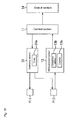
- FIG. 1 shows an explanatory diagram of a constitution of one embodiment of a touch sensor to which the present invention is applied;
- FIG. 2 shows an explanatory circuit diagram of a concept of the touch sensor of FIG. 1 ;
- FIG. 3 shows an explanatory diagram of functions which are realized by a microcomputer of FIG. 1 ;
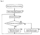
- FIG. 4 shows an explanatory flowchart of touch switching processing by the touch sensor of FIG. 1 ;
- FIG. 5 shows an explanatory flowchart of measurement processing by the touch sensor of FIG. 1 ;
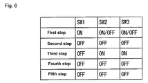
- FIG. 6 shows an explanatory table of the measurement processing by the touch sensor of FIG. 1 ;
- FIG. 7 shows an explanatory timing chart of the measurement processing by the touch sensor of FIG. 1 ;
- FIG. 8 shows an explanatory graph of a method for calculating unknown capacitance of a capacitor
- FIG. 9 shows an explanatory diagram of the method for calculating unknown capacitance of the capacitor
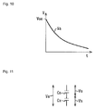
- FIG. 10 shows an explanatory graph of the method for calculating unknown capacitance of the capacitor
- FIG. 11 shows an explanatory diagram of the method for calculating unknown capacitance of the capacitor
- FIG. 12 shows an explanatory graph of the method for calculating unknown capacitance of the capacitor
- FIG. 13 shows an explanatory diagram of another constitution of the touch sensor
- FIG. 14 shows an explanatory diagram of a constitution of the touch sensor having the circuit constitution of FIG. 13 ;
- FIG. 15 shows an explanatory diagram of functions which are realized by a microcomputer of FIG. 14 ;
- FIG. 16 shows an explanatory flowchart of measurement processing by the touch sensor of FIG. 14 ;
- FIG. 17 shows an explanatory table of the measurement processing by the touch sensor of FIG. 14 ;
- FIG. 18 shows an explanatory timing chart of the measurement processing by the touch sensor of FIG. 14 ;
- FIG. 19 shows an explanatory diagram of another constitution of the touch sensor
- FIG. 20 shows an explanatory chart of operations of the touch sensor of FIG. 19 ;
- FIG. 21 shows an explanatory diagram of still another constitution of the touch sensor
- FIG. 22 shows an explanatory diagram of still another constitution of the touch sensor
- FIG. 23 shows an explanatory diagram of still another constitution of the touch sensor
- FIG. 24 shows an explanatory diagram of even another constitution of the touch sensor
- FIG. 25 shows an explanatory diagram of even another constitution of the touch sensor
- FIG. 26 shows an explanatory diagram even another constitution of the touch sensor
- FIG. 27 shows an explanatory diagram of functions which are realized by a microcomputer of FIG. 26 ;
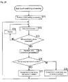
- FIG. 28 shows an explanatory flowchart of touch switching processing by the touch sensor of FIG. 26 ;
- FIG. 29 shows an explanatory flowchart of measurement processing by the touch sensor of FIG. 26 ;
- FIG. 30 shows an explanatory diagram of a constitution of a general purpose personal computer.
- a sensing apparatus includes a measurement section (for example, a measurement section 113 in FIG. 27 ) that measures capacitance of each of a plurality of first electric capacitors having unknown capacitance (for example, capacitors Cx 1 through Cx 4 in FIG. 26 ), a plurality of contact sections (for example, electrodes E 1 through E 4 in FIG. 26 ) that are electrically connected to the plurality of first electric capacitors and that a human body disposed proximally touches directly or indirectly through an insulator, a determination section (for example, a control section 112 in FIG.
- a storage section for example, a storage section 112 a in FIG. 27 ) that cumulatively stores a result of measurement for each of the plurality of first electric capacitors, which is a result of measurement by the measurement section
- a reference capacitance calculation section for example, a reference value calculation section 112 b in FIG.
- a difference calculation section (for example, a difference calculation section 112 c in FIG. 27 ) that calculates an absolute difference value between the reference capacitance for each of the plurality of first electric capacitors and the result of measurement for each of the plurality of first electric capacitors performed by the measurement section, and an adjustment section (for example, a threshold value adjustment section 112 d ) that adjusts the threshold value for each of the plurality of first electric capacitors based on a sum of the absolute difference value for each of the first electric capacitors calculated by the difference calculation section other than the absolute difference value of each of the first electric capacitors.
- the sensing apparatus can further include a third electric capacitor (for example, a capacitor Ca in FIG. 26 ) whose first end is connected to a second end of a circuit whose first end is grounded and which connects in series a second electric capacitor (for example, a capacitor Cs 11 in FIG. 26 ) having known capacitance and the first electric capacitors (for example, capacitors Cx 1 through Cx 4 in FIG. 26 ) and whose second end is grounded, to apply its own charging voltage to the second end of the circuit, thereby charging the first electric capacitors and the plurality of second electric capacitors having the known capacitance and respectively corresponding to the first electric capacitors, a first discharge section (for example, a switch SW 2 in FIG.
- a third electric capacitor for example, a capacitor Ca in FIG. 26
- a second discharge section for example, a switch SW 3 in FIG. 2
- a counter section for example, a counter 112 a in FIG. 27
- a comparison section for example, a comparison section 113 b in FIG.
- the measurement section (for example, a measurement section 113 in FIG. 27 ) can calculate the capacitance of the first electric capacitors based on the current number of times of discharge measured by the counter section, thereby measuring the capacitance of the first electric capacitors.
- the first discharge section can discharge the third electric capacitor (for example, the capacitor Ca in FIG. 26 ) which has been charged for a predetermined period of time (for example, from (time t(i+1) to time ti) after time t 1 in FIG. 7 ) through a resistor connected in series to the third electric capacitor, thereby discharging the third electric capacitor partly.
- a predetermined period of time for example, from (time t(i+1) to time ti) after time t 1 in FIG. 7 .
- a charge section that charges the third electric capacitor (for example, the capacitor Ca in FIG. 26 ) at a predetermined charging voltage can be further provided, wherein the charge section (for example, a power supply Vcc in FIG. 2 ) can charge the third electric capacitor directly.
- a charge section (for example, a power supply Vcc in FIG. 13 ) that charges the third electric capacitor at a predetermined charging voltage can be further provided, wherein the first discharge section has its first end grounded and its second end connected between the circuit and the resistor, and the charge section can charge the third electric capacitor from the same position as the second end of the first discharge section.
- a diode (for example, a diode D 21 in FIG. 26 ) can be provided in parallel with the resistor and in a forward direction toward the third electric capacitor.
- a switch section (for example, a switch section 101 in FIG. 27 ) can be further provided which switches one of the second electric capacitors having the known capacitance and the plurality of first electric capacitors in order to connect them in series.
- the adjustment section (the threshold value adjustment section 112 d in FIG. 27 ) can adjust the threshold value by subtracting from the threshold value for each of the first electric capacitors a value of the sum of the absolute difference value for each of the plurality of first electric capacitors calculated by the difference calculation section other than the absolute difference value of each of the first electric capacitors.
- a sensing method includes a measurement step (for example, step S 34 in FIG. 5 ) of measuring capacitance of each of a plurality of first electric capacitors having unknown capacitance, a determination step (for example, step S 75 and S 76 in FIG. 28 ) of determining whether a human body has touched the contact section either directly or indirectly based on a result of comparison between the capacitance of the plurality of first electric capacitors measured by the measurement section and a threshold value for each of the plurality of first electric capacitors, a storage step (for example, step S 91 in FIG.
- a reference capacitance calculation step for example, step S 92 in FIG. 29 ) of calculating reference capacitance for each of the plurality of first electric capacitors based on the result of measurement stored through processing of the storage section
- a difference calculation step for example, step S 93 in FIG. 29 ) of calculating an absolute difference value between the reference capacitance for each of the plurality of first electric capacitors and the result of measurement for each of the plurality of first electric capacitors performed through processing of the measurement step
- an adjustment step for example, step S 94 in FIG. 29 ) of adjusting the threshold value for each of the plurality of first electric capacitors based on a sum of the absolute difference value for each of the first electric capacitors calculated through processing of the difference calculation step other than the absolute difference value of each of the first electric capacitors.
- a sensing program is similar to the sensing method and so its description is not given.
- FIG. 1 shows an embodiment of a touch sensor to which the present invention is applied.
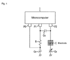
- a microcomputer 1 includes a central processing unit (CPU), a random access memory (RAM), a read only memory (ROM), and the like in such a configuration that the CPU may expand a predetermined program stored in the ROM in the RAM and executes it as required, thereby performing various kinds of processing. More specifically, by executing the program, the microcomputer 1 provides terminals P 0 to P 2 with a Hi signal or a Low signal as an output signal, to establish HiZ (high-impedance state, in which no input signal is received, thus resulting in the output signal being in neither the Hi state nor the Low state) and, as required, measures the input signal (a voltage at the terminal) and perform processing in accordance with a result of the measurement.
- CPU central processing unit
- RAM random access memory
- ROM read only memory
- the terminal P 0 is used to supply power with which a capacitor Ca is charged and, if regulated to the Hi state, applies a charging voltage to the capacitor Ca. It is to be noted that if regulated to the HiZ (high-impedance state), the terminal P 0 stops charging.
- the terminal P 1 is used to discharge the capacitor Ca through a resistor R and also discharges a capacitor Cs, and if regulated to the Low state, discharges the capacitors Ca and Cs, and if regulated to the HiZ state, stops discharging.
- the terminal P 2 is used to discharge a capacitor Cx and measures a charging voltage for the capacitor Cx, and if regulated to the Low state, discharges the capacitor Cx, and if regulated to the HiZ state, stops discharging the capacitor Cx, and if regulated to the Hi state, measures a charging voltage Vx for the capacitor Cx.
- the capacitor Ca is charged at a voltage applied from the terminal P 0 and discharged through the resistor R by the terminal P 1 .
- the capacitors Cs and Cx are connected in series and charged by the capacitor Ca.
- the capacitor Cx is an indication in a circuit configuration and indicates as an electric capacitor a target of measuring electrostatic capacitance such as a human body that touches an electrode E. Therefore, the capacitance of the capacitor Cx indicates electrostatic capacitance of a human body in a case where the human body has touched the electrode E and electrostatic capacitance in a non-contact condition in a case where a human body has not touched the electrode E.
- the electrode E may have such a constitution that a human body can touch it directly or touch it indirectly through an insulator.
- the electrode E used here is such a type that a human body can touch it indirectly through an insulator; however, of course, it is needless to say that the electrode may be such a type that a human body can touch it directly.
- a change in electrostatic capacitance difference in electrostatic capacitance of the capacitor Cx between the case of contact and the case of non-contact
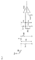
- FIG. 2 is an explanatory circuit diagram of the concept of the touch sensor of FIG. 1 .
- Switches SW 1 through SW 3 straightforwardly indicate the operating states of the terminals P 0 through P 2 respectively. That is, if the terminal P 0 is regulated to the Hi state, the switch SW 1 in the circuit of FIG. 2 turns ON, resulting in a power supply Vcc charging the capacitor Ca at a charging voltage Vcc. On the other hand, if the terminal P 0 is regulated to the HiZ state, the switch SW 0 turns OFF. Further, if the terminal P 1 is regulated to the Low state, the switch SW 2 in the circuit of the figure turns ON, and if regulated to the HiZ state, the switch SW 2 turns OFF.
- a comparator Comp compares a charging voltage Vx for the capacitor Cx to a reference voltage Vref and outputs a result of the comparison. It is to be noted that the comparator Comp is not an actual comparator circuit but is a function which is realized by the later-described microcomputer 1 .
- charging voltages for the capacitors Ca, Cs, and Cx will be indicated by Va, Vs, and Vx respectively.
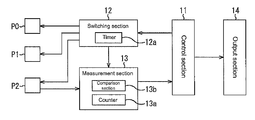
- a control section 11 controls the entire operation of the microcomputer 1 , and when instructed by an operation section (not shown), causes a switching section 12 to control the operations of the terminals P 0 through P 2 . Further, the control section 11 determines whether a human body came in contact based on a result of measurement of the electrostatic capacitance of the capacitor Cx by a measurement section 13 and controls an output section 14 including a cathode ray tube (CRT), a liquid crystal display (LCD), or a speaker so that the output section 13 presents a result of determination on whether the human body has come in contact or not.
- CTR cathode ray tube
- LCD liquid crystal display
- the terminal P 0 When supplied with a Hi-state signal from the switching section 12 , the terminal P 0 causes the power supply Vcc to charge the capacitor Ca at the charging voltage Vcc as in a case where the switch SW 1 of FIG. 2 is turned ON, which is not shown in FIG. 3 . Also, if regulated to the HiZ state by the switching section 12 , the terminal P 0 causes the power supply Vcc to stop supplying power to the capacitor Ca as in a case where the switch SW 1 in FIG. 2 is turned OFF.
- the terminal P 1 turns ON the switch SW 2 in FIG. 2 to gradually discharge the capacitor Ca through the resistor R from the grounding point and instantaneously discharges the capacitor Cs totally from the grounding point. Further, if regulated to the HiZ state by the switching section 12 , the terminal P 1 turns OFF the switch SW 2 in FIG. 2 to connect the capacitor Ca and a combined capacitor of the capacitors Cs and Cx in parallel.
- the terminal P 2 If regulated to the Low state by the switching section 12 , the terminal P 2 turns ON the switch SW 3 in FIG. 2 to discharge the capacitor Cx. Also, if regulated to the HiZ state by the switching section 12 , the terminal P 2 turns OFF the switch SW 3 to hold the capacitor Cx in a charged condition. Further, if regulated to the Hi state by the switching section 12 , the terminal P 2 measures a charging voltage of the capacitor Cx.
- the switching section 12 controls the operations of the terminals P 0 through P 2 at predetermined intervals by referencing a built-in timer 12 a . More specifically, at predetermined intervals, the switching section 12 periodically switches the terminals P 0 through P 2 to the Hi, HiZ, or Low state in a predetermined pattern. Further, each time one cycle of the operations repeated in the predetermined pattern ends, the switching section 12 supplies the measurement section 13 with a signal to that effect.
- the measurement section 13 measures the charging voltage Vx for the capacitor Cx supplied from the terminal P 2 and compares it to the reference voltage Vref, and if it agrees with the reference voltage Vref or smaller than it, measures electrostatic capacitance based on the current processing count n stored in a counter 13 a , electrostatic capacitance of the capacitors Ca and Cs, resistance of the resistor R, and the charging voltage Vcc of the power supply Vcc.
- the counter 13 a of the measurement section 13 counts cycle count (number of times of repetitive processing) n based on a signal supplied from the switching section 12 each time the operations are repeated in the predetermined pattern, and to average the processing counts n, counts calculated count m of the processing count n and a total sum N of m number of times of processing count n.
- a comparison section 13 b which corresponds in constitution to the comparator Comp in FIG. 2 , compares the charging voltage Vx supplied from the terminal P 2 to the reference voltage Vref, and if the charging voltage Vx agrees with the reference voltage Vref or smaller than it, calculates electrostatic capacitance of the capacitor Cx based on the current processing count n stored in the counter 13 a , electrostatic capacitance of the capacitors Ca and Cs, resistance of the resistor R, and the charging voltage Vcc of the power supply Vcc and outputs it to the control section 11 as a measurement result for the capacitor Cx.
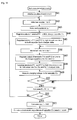
- step S 1 the control section 11 initializes the operation states of the switching section 12 and the measurement section 13 .
- step S 2 the control section 11 causes the switching section 12 to perform switching so that the measurement section 13 measures electrostatic capacitance of the capacitor Cx.
- step S 21 the measurement section 13 initializes the counters m and N of the counter 13 a to 0.
- step S 22 the measurement section 13 initializes the counter n of the counter 13 a to 0.
- step S 23 the counter 13 a of the measurement section 13 increments the counter m by 1.
- step S 26 the counter 13 a of the measurement section 13 increments the counter n by 1.
- step S 27 the switching section 12 regulates the terminal P 0 to HiZ and the terminals P 1 and P 2 to Low for a predetermined period of time based on the timer 12 a , thereby discharging the capacitors Ca, Cs, and Cx.
- the capacitors Cs and Cx are discharged through the ground instantaneously, whereas the capacitor Ca is discharged by the SW 2 through the resistor R to the ground gradually and therefore, will be discharged only partly within a predetermined time t.
- step S 28 the switching section 12 regulates the terminals P 0 through P 2 to the HiZ state for a predetermined time t based on the timer 12 a to transfer charge in the capacitor Ca (charge left in a condition where it is partly discharged by the processing in step S 27 ) to the capacitors Cs and Cx, thereby holding the capacitors Ca, Cs, and Cx in a charged state.
- the charging voltage Va for the capacitor Ca will be equal to a sum of the charging voltages Vs and Vx for the capacitors Cs and Cx respectively.
- the ratio between the charging voltages Vs and Vx for the capacitors Cs and Cx will be a ratio between reciprocals of capacitance values of the capacitors Cs and Cx.
- step S 29 the switching section 12 regulates the terminal P 2 to the Hi state for the predetermined time t based on the timer 12 a so that the measurement section 13 measures a charging voltage Vx for the capacitor Cx through the terminal P 2 for the predetermined time t, thereby acquiring the charging voltage for the capacitor Cx.
- step S 30 the comparison section 13 b of the measurement section 13 determines whether a measured value of the charging voltage Vx for the capacitor Cx is smaller than the reference voltage Vref. For example, if it is determined that the charging voltage Vx is not smaller than the reference voltage Vref, the process returns to step S 26 . That is, until it is determined in step S 30 that the charging voltage Vx is smaller than the reference voltage Vref, processing of steps 26 to 30 will be repeated, and the value of the counter n is incremented each time the processing is repeated.
- step S 30 If it is determined in step S 30 that the charging voltage Vx is smaller than the reference voltage Vref, in step S 31 , the measurement section 13 adds a freshly obtained processing count n to the total sum N of the number of times the processing of steps S 26 to S 30 is repeated.
- step S 32 the measurement section 13 determines whether a value of repetitive processing count n obtained by the counter m is at least a predetermined upper limit value M of the counter m, and if it is determined that the counter m is less than the upper limit value M, the process returns to step S 22 . That is, until the value of the counter m is at least the upper limit value M, the processing of steps S 22 to S 32 will be repeated.
- step S 33 the measurement section 13 obtains as count an average value of M number of times of the processing counts n through the processing of steps S 26 to S 30 repeated until the charging voltage Vx for the capacitor Cx falls to the reference voltage Vref.
- step S 33 the measurement section 13 calculates an electrostatic capacitance value of the capacitor Cx based on an average value count of the processing counts n, capacitance values of the capacitors Ca and Cs, predetermined times t for which the processing of steps S 25 , S 27 , and S 28 are performed, the charging voltage Vcc of the power supply Vcc, and the reference voltage Vref and outputs the electrostatic capacitance value of the capacitor Cx to the control section 11 , thus ending the measurement processing.
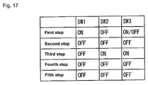
- step S 24 the processing of the first step of FIG. 6 is performed, that is, the switch SW 1 of FIG. 2 is turned ON.
- This processing merely charges the capacitor Ca, and therefore the switches SW 2 and SW 3 may be in the ON state or the OFF state.
- the switches SW 2 and SW 3 are in the ON state (with the terminals P 1 and P 2 at Low)
- a bold solid line indicates the charging voltage Va for the capacitor Ca and a dotted line indicates the charging voltage Vx for the capacitor Cx.
- the operation state of the terminal P 2 is shown for measuring (the charging voltage Vx) for the capacitor Cx by the measurement section 13 through the terminal P 2 , in which HiZ indicates a high-impedance state, that is, a state where the terminal P 2 is providing no output, and OUT_L indicates a state where it is set to Low.
- the operation state of the terminal P 1 is shown, in which HiZ indicates a high-impedance state, that is, a state where the terminal P 1 is providing no output and OUT_L indicates a state where it is set to Low.
- the operation state of the terminal P 0 is shown, in which HiZ indicates a high-impedance state, that is, a state where the terminal P 0 is providing no output, and OUT_L indicates a state where it is set to Low.
- the operation states of the switches SW 3 to SW 1 are shown respectively.
- the switch SW 1 operates in conjunction with the terminal P 0 such that the switch SW 1 is turned ON only when the terminal P 0 is set to Hi and, otherwise, in the OFF state.
- the switches SW 2 and SW 3 operate in conjunction with the terminals P 1 and P 2 such that the switches SW 2 and SW 3 are turned ON only when the terminals P 1 and P 2 are set to Low and, otherwise, in the OFF state respectively
- various processing timings shown in FIG. 7 for example, even the same timing in FIG. 7 may fluctuate temporally through a processing procedure depending on a program installed in the microcomputer 1 ; however, the fluctuation can be ignored sufficiently in terms of the whole operations.
- step S 25 the processing of the second step of FIG. 6 is performed, that is, the switches SW 1 to SW 3 of FIG. 2 are turned OFF.
- step S 27 the processing of the third step of FIG. 6 is performed, that is, the switch SW 1 of FIG. 2 is turned OFF and the switches SW 2 and SW 3 are turned ON.
- the terminals P 1 and P 2 are regulated to Low to turn ON the switches SW 2 and SW 3 of FIG. 2 , thereby discharging the capacitors Cx and Cs totally and gradually discharging the capacitor Ca through the resistor R only partly.
- step S 28 the processing of the fourth step of FIG. 6 is performed, that is, the switches SW 1 to SW 3 of FIG. 2 are turned OFF.
- the capacitor Ca is partly discharged through the resistor R between time t 2 and time t 3 (for a time t), and then charges still left on the capacitor Ca causes the capacitors Ca, Cs, and Cx to be held in a charged state. That is, as the capacitor Ca is partly discharged between time t 2 and time t 3 , the charging voltage Va for the capacitor Ca decreases as shown in FIG. 7 .
- the charging voltage Vx applied on the capacitor Cx is also reduced correspondingly below an initial value of the charging voltage V_hi.
- the ratio between the respective charging voltages Vs and Vx for the capacitors Cs and Cx is kept constant.
- step S 29 the processing of the fifth step of FIG. 6 is performed, that is, unless a value of the charging voltage Vx for the capacitor Cx measured by the measurement section 13 through the terminal P 2 at time t 4 in a condition where the switches SW 1 to SW 3 of FIG. 2 remain in the OFF state is smaller than the reference voltage Vref, the processing of steps S 26 to S 30 , that is, the processing of the third through fifth steps of FIG. 6 will be repeated.
- the charging voltage Vx for the capacitor Cx since the sum of the charging voltage Vx for the capacitor Cx and the charging voltage Vs for the capacitor Cs is equal to the charging voltage Va for the capacitor Ca, when the charging voltage Va for the capacitor Ca is decreased as the processing of the third through fifth steps is repeated, the charging voltage Vx for the capacitor Cx will also continue to decrease in a condition where its ratio with respect to the charging voltage Va for the capacitor Ca is kept constant.
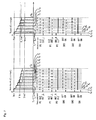
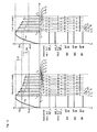
- a thin line indicates the charging voltage Va for the capacitor Ca
- a bold line indicates a change in the charging voltage Vx in a case where the electrostatic capacitance of the capacitor Cx is 10 pF
- a dotted line indicates a change in the charging voltage Vx in a case where the electrostatic capacitance of the capacitor Cx is 11 pF.
- the capacitor Cs has electrostatic capacitance of 12 pF
- the resistor R has resistance of 10 k ⁇
- the capacitor Ca has electrostatic capacitance of 0.1 ⁇ F
- the electrostatic capacitance of the capacitor Cx is obtained from the number of times of repetitive processing count of the processing of the third through fifth steps of the above-described FIG. 6 .
- Vx VCC ((1/ Cx )/((1/ Cx )+(1/ Cs )) ⁇ e ⁇ ( ⁇ (count ⁇ 3 t )/( Ca ⁇ R )) (3)
- V ref Vcc ((1/ Cx )/((1/ Cx )+(1/ Cs )) ⁇ e ⁇ ( ⁇ (count ⁇ 3 t )/( Ca ⁇ R )) (4)
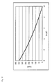
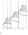
- a relationship between the capacitor Cx and the number of times of processing count will be such as shown in FIG. 12 when, for example, the capacitor Cs has electrostatic capacitance of 10 pF, the resistor R has resistance of 10 k ⁇ , the capacitor Ca has electrostatic capacitance of 0.1 ⁇ F, and the time t is 2 ⁇ s.
- the electrostatic capacitance of the capacitor Cx is in the vicinity of 8 pF, electrostatic capacitance Cx is obtained at a resolution/pF of about 20 as referred to the number of times of processing count.
- the electrostatic capacitance of the capacitor Cx is obtained from the above Equation (5) on a condition that the charging voltage Vx for the capacitor Cx is lowered through the repetitive processing so as to agree with the reference voltage Vref, so that it is assumed that the charging voltage Vx for the capacitor Cx at an initial charging should be larger than the reference voltage Vref. Therefore, the reference voltage Vref needs to satisfy the following Equation (6): V ref/ Vcc ⁇ (1/ Cs )/((1/ Cx )+(1/ Cs )) (6)
- the number of times of processing can be reduced and, by that much, the time t can be decreased to enhance the resolution.
- processing of steps S 31 to S 33 in the flowchart of FIG. 5 is used to obtain an average value of M number of times of processing count n as the number of processing count, so that even if, for example, ripple noise occurs in one measurement, the processing count can be obtained accurately. It is to be noted that if no ripple noise is found in ripple noise occurrence detection, the processing speed may be increased by decreasing the number of times of repeating the processing required to obtain an average value by setting M to 1.
- step S 3 the control section 11 determines whether a human body has touched the electrode E based on unknown electrostatic capacitance of the capacitor Cx supplied from the measurement section 13 . More specifically, since the electrostatic capacitance of the human body is in the vicinity of 11 pF, the control section 11 can determine whether the human body has touched the electrode E by determining whether the electrostatic capacitance of the capacitor Cx supplied from the measurement section 13 is at a threshold value Cxth in the vicinity of 11 pF.
- the control section 11 determines that the human body has come in contact when the electrostatic capacitance Cx of the capacitor Cx is equal to Cxth, i.e., (11 ⁇ 0.95) pF ⁇ Cxth ⁇ (11 ⁇ 1.05) pF, and otherwise, determines that the human body has not come in contact.
- step S 4 the control section 11 controls the output section 14 to indicate contact of the human body and the process returns to step S 2 .
- step S 5 the control section 11 controls the output section 14 to indicate non-contact of the human body, and the process returns to step S 2 to repeat the subsequent processing.
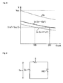
- the touch sensor of FIG. 1 has such a circuit configuration that the switches SW 1 and SW 2 sandwich the resistor R as shown in FIG. 2 , so that they cannot be controlled with the same terminal.
- the switch SW 1 is connected at an opposite position with respect to the resistor R as shown in FIG. 13 , the switches SW 1 and SW 2 can be controlled with one terminal.
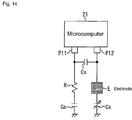
- FIG. 14 shows such a configuration of the touch sensor that the switches SW 1 and SW 2 can be controlled with one terminal.
- a microcomputer 21 has two terminals P 11 and P 12 .
- the terminal P 12 has the same functions as the terminal P 2 of the microcomputer 1 of FIG. 1
- the terminal P 11 in FIG. 14 has combined functions of both the terminals P 0 and P 1 in FIG. 1 . It is to be noted that the same components of FIG. 14 as those of FIG. 1 are indicated by the same symbols and description thereof will not be given as appropriate.
- the terminal P 11 turns ON a switch SW 1 of FIG. 13 , thus charging a capacitor Ca at a supply voltage Vcc of a power supply Vcc. If set to the HiZ state by the switching section 31 , the terminal P 11 turns OFF switches SW 1 and SW 2 of FIG. 13 as well as the SW 2 of FIG. 2 , thus connecting the capacitor Ca and a combined capacitor of capacitors Cs and Cx in parallel. Further, if set to the Low state by the switching section 31 , the terminal P 11 turns ON the switch SW 2 of FIG. 13 , thus gradually discharging the capacitor Ca through a resistor R from the grounding point and instantaneously discharging the capacitor Cs totally. It is to be noted that the terminal P 12 is similar to the terminal P 2 of FIG. 1 and its description will not be given.
- the switching section 31 basically has the same functions as the switching section 12 of FIG. 3 in that it will control the operations of the terminals P 11 and P 12 at predetermined intervals by referencing a built-in timer 31 a . More specifically, the switching section 31 repetitively switches the operating states of the terminals P 11 and P 12 in a predetermined pattern cyclically at the predetermined intervals. Further, each time one cycle of the operations repeated in the predetermined pattern ends, the switching section 31 supplies the measurement section 13 with a signal to that effect.
- step S 2 by the touch sensor of FIG. 14 will be described with reference to the flowchart of FIG. 16 because only the measurement processing is different from that in the processing described with reference to the flowchart of FIG. 4 .
- steps S 41 to S 43 and steps S 49 to S 54 in the flowchart of FIG. 16 is the same as that of steps S 21 to S 23 and steps S 29 to S 34 described with reference to the flowchart of FIG. 5 and description thereof will not be given.
- step S 44 the switching section 31 regulates the output of the terminal P 11 to Hi, thus charging the capacitor Ca with the power supply Vcc. That is, by regulating the output of the terminal P 11 to Hi, the switch SW 1 shown in FIG. 13 is turned ON to supply the capacitor Ca with power through the resistor R from the power supply Vcc so that the capacitor Ca is gradually charged up to the charging voltage Vcc finally.
- step S 46 the counter 13 a of the measurement section 13 increments a counter n by 1.
- step S 47 the switching section 31 regulates the terminals P 11 and P 12 to Low for a predetermined time t based on the timer 31 a , thereby discharging the capacitors Ca, Cs, and Cx.
- the capacitors Cs and Cx are discharged through the ground instantaneously, whereas the capacitor Ca is discharged by the switch SW 2 through the resistor R to the ground gradually, and therefore, will be discharged only partly within a predetermined time t.
- step S 48 the switching section 31 regulates the terminals P 11 and P 12 to the HiZ state for a predetermined time t based on the timer 31 a to transfer charges in the capacitor Ca (charges left in a condition where the charges are partly discharged by the processing of step S 47 ) to the capacitors Cs and Cx, thereby holding the capacitors Ca, Cs, and Cx in a charged state.
- the charging voltage Va for the capacitor Ca is equal to a sum of the charging voltages Vs and Vx for each capacitor Cs and Cx.
- the ratio between the charging voltages Vs and Vx for the capacitors Cs and Cx is that between the reciprocals of capacitance values of the capacitors Cs and Cx.
- step S 44 the first step processing in FIG. 17 is performed, that is, the switch SW 1 in FIG. 13 is turned ON.
- This processing only charges the capacitor Ca, so that the switch SW 2 is turned OFF and the switch SW 3 may be either turned ON or OFF.
- FIG. 7 in the touch sensor of FIG.
- the charging voltage Va for the capacitor Ca reaches Vcc at the same time as the switch SW 1 is turned ON, whereas in the touch sensor in FIG. 14 , as shown in FIG. 18 , power of the power supply Vcc is supplied to the capacitor Ca through the resistor R, so that it takes some time to charge the capacitor.
- a bold solid line indicates the charging voltage Va for the capacitor Ca
- a dotted line indicates the charging voltage for the capacitor Cx.
- the operation state of the terminal P 12 is shown for measuring the capacitor Cx by the measurement section 13 through the terminal P 12 , in which HiZ indicates a high-impedance state, that is, a state where the terminal P 12 is providing no output and OUT_L indicates a state where it is set to Low.
- Hi indicates a state where the capacitor Ca is supplied with power through the terminal P 11 from the power supply Vcc and being charged at the charging voltage Vcc.
- HiZ indicates a high-impedance state, that is, a state where the terminal P 11 is providing no output, and OUT_L indicates a state where it is set to Low.
- the operation states of the switches SW 3 to SW 1 are shown respectively.
- the switch SW 1 operates in conjunction with the terminal P 11 such that the switch SW 1 is turned ON when the terminal P 11 is set to Hi, and that the switch SW 1 is turned OFF when the terminal P 11 is in the HiZ state, and when the terminal P 11 is set to Low, the switch SW 2 is turned ON. It is thus possible to control the switches SW 1 and SW 2 by using only the terminal P 11 .
- the switch SW 3 operates in conjunction with the terminal P 12 such that the switch SW 3 is turned ON only when the terminal P 12 is set to Low, and otherwise, in the OFF state.
- step S 45 the processing of the second step of FIG. 17 is performed, that is, the switches SW 1 and SW 2 of FIG. 13 are turned OFF.
- step S 47 the processing of the third step of FIG. 17 is performed, that is, the switch SW 1 of FIG. 13 is turned OFF and the switches SW 2 and SW 3 are turned ON.
- the terminal P 11 is regulated to Low to turn ON the switches SW 2 and SW 3 of FIG. 13 , thereby discharging the capacitors Cx and Cs totally and gradually discharging the capacitor Ca through the resistor R.
- step S 48 the processing of the fourth step of FIG. 17 is performed, that is, the switches SW 1 to SW 3 of FIG. 13 are turned OFF.
- step S 49 the processing of the fifth step of FIG. 17 is performed. That is, if a value of the charging voltage Vx for the capacitor Cx measured by the measurement section 13 through the terminal P 12 at time t 4 in a condition where the switches SW 1 to SW 3 of FIG. 13 are in the OFF state is not smaller than a reference voltage Vref, the processing of steps S 46 to S 50 , that is, the processing of the third through fifth steps of FIG. 17 will be repeated.
- the touch sensor of FIG. 14 not only can detect contact/non-contact of a human body speedily and accurately but also has only two terminals to be controlled by the microcomputer 21 , thereby reducing the manufacturing costs.
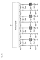
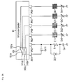
- a plurality of configurations of the touch sensor in FIG. 14 may be provided so that contact/non-contact of a human body may be detected at a plurality of positions by using a plurality of electrodes.
- capacitors Ca 1 to Ca 4 correspond to the capacitor Ca in FIG. 14
- capacitors Cs 1 to Cs 4 correspond to the capacitor Cs in FIG. 14
- capacitors Cx 1 to Cx 4 correspond to the capacitor Cx in FIG. 14
- resistors R 1 to R 4 correspond to the resistor R in FIG. 14
- electrodes E 1 to E 4 correspond to the electrode E in FIG. 14 , which are identical to each other respectively.
- the corresponding microcomputer 51 is provided with eight terminals of terminals P 21 to P 28 , of which terminals P 21 , P 23 , P 25 , and P 27 correspond to the terminal 11 , and terminals P 22 , P 24 , P 26 , and P 28 correspond to the terminal 12 , which are identical to each other respectively.
- the microcomputer 51 measures contact/non-contact of a human body on the electrode E 1 by using the terminals P 21 and P 22 , on the electrode E 2 by using the terminals P 23 and P 24 , on the electrode E 3 by using the terminals P 25 and P 26 , and on the electrode E 4 by using the terminals P 27 and P 28 .
- the microcomputer 51 does not simultaneously measure the charging voltages Vx 1 to Vc 4 for the capacitors Cx 1 to Cx 4 at the terminals P 22 , P 24 , P 26 , and P 28 respectively, but, for example, measures contact/non-contact of a human body on the electrode E 1 by using the terminals P 21 and P 22 , on the electrode E 2 by using the terminals P 23 and P 24 , on the electrode E 3 by using the terminals P 25 and P 26 , and on the electrode E 4 by using the terminals P 27 and P 28 in this order.
- contact/non-contact of a human body on the electrodes E 1 to E 4 is detected sequentially.
- the capacitors Ca 1 to Ca 4 take a longer time to be charged owing to the respective resistors R 1 to R 4 , so that if they start to be charged after their capacitance values are obtained, a charge waiting time occurs, thus possibly taking too long processing time.
- the capacitor Ca whose electrostatic capacitance is to be calculated next may start to be charged. That is, for example, as shown in an upper part of FIG. 20 , the microcomputer 51 charges the capacitor Ca 1 using the terminals P 21 and P 22 between times T 0 and T 100 and starts processing to repeat the processing of the third through fifth steps in FIG. 17 at time T 100 . In this case, after time t 100 , immediately after starting the processing to repeat the processing of the third through fifth steps in FIG. 17 , to obtain electrostatic capacitance of the capacitor Cx 2 as shown by a middle part of FIG.
- the microcomputer 51 starts charging the capacitor Ca 2 using the terminals P 23 and P 24 at, for example, time t 200 . Then, the capacitor Ca 2 has been charged completely at time t 210 when electrostatic capacitance of the capacitor Cx 1 was obtained, so that the microcomputer 51 starts the processing to repeat the processing of the third through fifth steps in FIG. 17 to obtain electrostatic capacitance of the capacitor Cx 2 . Similarly, immediately after starting the processing to repeat the processing of the third through fifth steps in FIG. 17 , to obtain electrostatic capacitance of the capacitor Cx 3 , the microcomputer 51 starts charging the capacitor Ca 3 using the terminals P 25 and P 26 at, for example, time t 300 .
- the capacitor Ca 3 has been charged completely at time t 310 when electrostatic capacitance of the capacitor Cx 2 was obtained, so that the microcomputer 51 starts the processing to repeat the processing of the third through fifth steps in FIG. 17 to obtain electrostatic capacitance of the capacitor Cx 3 .
- the capacitors Ca 1 to Ca 4 corresponding to the electrodes to be processed next are charged to reduce the waiting time due to charging, thereby speedily detecting contact/non-contact of a human body with high accuracy even in the case of the detection of the human body contact/non-contact at a plurality of positions.
- the microcomputer does not perform processing by use of three terminals or more at a time.
- the capacitor Ca and the resistor R are only charged first and then discharged by the repetitive processing, so that they may be connected in parallel with a plurality of capacitors Cs and Cx and the electrode E. Therefore, for example, as shown in FIG.
- each of terminal P 31 including a capacitors Cs 1 and Cx 1 to detect human body contact/non-contact at an electrode E 1 and terminal P 33 including capacitors Cs 2 and Cx 2 to detect human body contact/non-contact at an electrode E 2 may be connected in parallel
- each of terminal P 34 including capacitors Cs 3 and Cx 3 to detect human body contact/non-contact at an electrode E 3 and terminal P 36 including capacitors Cs 4 and Cx 4 to detect human body contact/non-contact at an electrode E 4 may be connected in parallel.
- a microcomputer 61 measures human body contact/non-contact on the electrode E 1 by controlling the terminals P 31 and P 32 , on the electrode E 2 by controlling the terminals P 32 and P 33 , on the electrode E 3 by controlling the terminals P 34 and P 35 , and on the electrode E 4 by controlling the terminals P 35 and P 36 .
- the microcomputer 61 can control a touch sensor that detects human body contact/non-contact at four positions by using six terminals, thus reducing the costs for manufacturing the touch sensor.
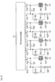
- a touch sensor of FIG. 22 includes a terminal P 41 that corresponds to the terminal P 0 in FIG. 1 , a terminal 42 that corresponds to the terminal P 1 in FIG. 1 , a resistor R, and a capacitor Ca in such a configuration that four terminals each corresponding to the terminal P 2 are disposed in parallel.
- a terminal P 43 To a terminal P 43 are connected capacitors Cs 1 and Cx 1 to detect human body contact/non-contact on an electrode E 1 , to a terminal P 44 are connected capacitors Cs 2 and Cx 2 to detect human body contact/non-contact on an electrode E 2 , to a terminal P 45 are connected capacitors Cs 3 and Cx 3 to detect human body contact/non-contact on an electrode E 3 , and to a terminal P 46 are connected capacitors Cs 4 and Cx 4 to detect human body contact/non-contact on an electrode E 4 .
- a microcomputer 71 measures human body contact/non-contact on the electrode E 1 by controlling the terminals P 41 to P 43 , on the electrode E 2 by controlling the terminals P 41 , P 42 , and P 44 , on the electrode E 3 by controlling the terminals P 41 , P 42 , and P 45 , and on the electrode E 4 by controlling the terminals P 41 , P 42 , and P 46 .
- the microcomputer 71 can control a touch sensor that detects human body contact/non-contact at four positions by using six terminals.
- a charging time is delayed due to charging through the resistors R 1 to R 4 .
- such a configuration may be provided as to charge the capacitors Ca 1 to Ca 4 not through the resistors R 1 to R 4 , thereby reducing the charging time.
- the charging time for the capacitors Ca 1 and Ca 2 may be reduced.
- the touch sensor of FIG. 22 will take such a touch sensor configuration as shown in FIG. 25 .
- the touch sensor of FIG. 25 is different from that of FIG. 22 in that a microcomputer 81 is substituted for the microcomputer 71 , and that the diode D 21 is disposed in parallel with the resistor R.
- the touch sensor of FIG. 25 the necessity of the terminal P 41 is eliminated in contrast to the case of FIG. 22 , so that the microcomputer 81 can measure capacitance of capacitors Cx 1 to Cx 4 by using five terminals of P 51 to P 55 . It is to be noted that processing to measure the capacitance of each of the capacitors Cx 1 to Cx 4 by using the touch sensor of FIG. 25 only repeats measurement processing by the touch sensor of FIG. 14 four times, and the description of its operations will not be given.
- Such a touch sensor as shown in FIG. 25 can reduce the charging time and so speedily measure the capacitance of the capacitors Cx 1 to Cx 4 and also decrease the number of components by decreasing the number of the terminals, thereby reducing the costs for manufacturing.
- capacitors Cs 1 to Cs 4 having known capacitance are provided to measure the capacitance of the capacitors Cx 1 to Cx 4 , measurement processing is performed on the capacitors Cx 1 to Cx 4 independently of each other, so that a common capacitor with known capacitance may be provided and used by switching it at the timing of the measurement processing of each of the capacitors Cx 1 to Cx 4 .
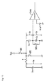
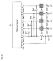
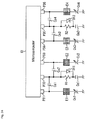
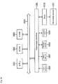
- FIG. 26 shows a configuration example of an embodiment of the touch sensor in which a common capacitor with known capacitance is provided and used by switching it at the timing of measurement processing of each of capacitors Cx 1 to Cx 4 . It is to be noted that in the touch sensor of FIG. 26 , components similar to those of the touch sensor of FIG. 25 are indicated by the same symbols, and description thereof will not be given as appropriate.
- the touch sensor of FIG. 26 is different from that of FIG. 25 in that a microcomputer 91 is substituted for the microcomputer 81 , a capacitor Cs 11 is substituted for the capacitors Cs 1 to Cs 4 , and the microcomputer 91 realizes a switch section 101 .
- the switch section 101 has a first end thereof connected to a terminal 101 a connected to a terminal P 61 and a second end thereof switched to any of terminals 101 b to 101 e .
- the terminals 101 b to 101 e of the switch section 101 are connected to terminals P 63 to P 66 of the microcomputer 91 respectively.
- the capacitor Cs 11 has a first end thereof connected to the terminal P 61 and a second end thereof connected to a terminal P 62 . It is to be noted that the switch section 101 is a function realized by the microcomputer 91 and not actually provided as hardware.
- the microcomputer 91 when measuring electrostatic capacitance of the capacitor Cx 1 , the microcomputer 91 connects the switch section 101 to the terminal 101 b to use the capacitor Cs 11 in place of the capacitor Cs 1 in FIG. 25 , thereby measuring the electrostatic capacitance of the capacitor Cx 1 . Also, similarly when measuring electrostatic capacitance of the capacitors Cx 2 to Cs 4 , the microcomputer 91 connects the switch section 101 to the terminals 101 c to 101 e to use the capacitor Cs 11 in place of the capacitor Cs 2 to Cs 4 in FIG. 25 , thereby measuring the electrostatic capacitance of the capacitors Cx 2 to Cx 4 , respectively.
- any number of target capacitors including the capacitors Cx 1 to Cx 4 can be measured as long as there is one capacitor Cs having known capacitance, to decrease the number of components, thereby reducing the costs.
- erroneous detection may be reduced by adjusting threshold values Cx 1 th to Cx 4 th over which human body contact on the electrodes E 1 to E 4 is detected, based on the electrostatic capacitance of the plurality of capacitors Cx 1 to Cx 4 , respectively.
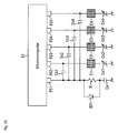
- FIG. 27 shows a constitution example of functions which are realized by the microcomputer 91 in the touch sensor of FIG. 26 in which the threshold values Cx 1 th to Cx 4 th over which human body contact on the electrodes E 1 to E 4 is detected are adjusted based on the electrostatic capacitance of the plurality of capacitors Cx 1 to Cx 4 , respectively. It is to be noted that in FIG. 27 , the functions similar to those shown in FIG. 15 are indicated by the same symbols and description thereof will not be given as appropriate.
- FIG. 27 is different from FIG. 15 in that a switching section 111 , a control section 112 , and a measurement section 113 are substituted for the control section 11 , the measurement section 13 , and the switching section 31 .
- the switching section 111 switches the operations of terminals P 61 to P 66 in accordance with the operations of a timer 111 a and also controls the operations of a switch section 101 .
- the measurement section 113 which realizes substantially the same functions as the measurement section 13 , measures electrostatic capacitance values of the respective capacitors Cx 1 to Cx 4 corresponding to the electrodes E 1 to E 4 based on output signals from the terminals P 61 and P 63 to P 66 and supplies results of the measurement to the control section 112 .
- the control section 112 realizes basically the same functions as the control section 11 , including a storage section 112 a , a reference value calculation section 112 b , a difference calculation section 112 c , and a threshold value adjustment section 112 d .
- the control section 112 detects human body contact/non-contact on the electrodes E 1 to E 4 based on the capacitors Cx 1 to Cx 4 supplied from the measurement section 113 and the corresponding threshold values Cx 1 th to Cx 4 th respectively and adjusts the threshold values Cx 1 th to Cx 4 th based on the capacitors Cx 1 to Cx 4 respectively.
- the storage section 112 a stores a predetermined number of immediately previous measurement results out of those of the capacitors Cx 1 to Cx 4 .
- the reference value calculation section 112 b obtains an average value of the predetermined number of immediately previous measurement results of the capacitors Cx 1 to Cx 4 stored in the storage section 112 a as reference values Cx 1 ave through Cx 4 ave of the capacitors Cx 1 to Cx 4 .
- the difference calculation section 112 c obtains absolute difference values ⁇ Cx 1 through ⁇ Cx 4 between the reference values Cx 1 ave through Cx 4 ave and the electrostatic capacitance values Cx 1 to Cx 4 of the capacitors Cx 1 to Cx 4 , which are the latest measurement results, respectively.
- the threshold value adjustment section 112 d adjusts the threshold values Cx 1 th through Cx 4 th based on the absolute difference values ⁇ Cx 1 to ⁇ Cx 4 respectively.
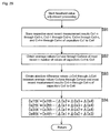
- step S 72 the control section 112 determines in step S 73 whether the measurement processing is finished for all of the capacitors Cx 1 to Cx 4 , and if determines that the measurement processing has not been finished for all of them, controls the switching section 111 in step S 74 to connect the switch section 101 to any one of terminals 101 c to 101 e , and the processing returns to step S 72 . That is, the switch section 101 is switched to the terminals 101 b to 101 e sequentially until electrostatic capacitance of each of the capacitors Cx 1 to Cx 4 is obtained through the measurement processing, thus repeating the processing of steps S 72 to S 74 .
- step S 75 when the measurement section 113 obtains electrostatic capacitance of each of the capacitors Cx 1 to Cx 4 and supplies the value to the control section 112 in step S 73 , threshold value adjustment processing is performed in step S 75 .
- step S 91 the control section 112 adds to the storage section 112 a the respective most recent measurement results Cx 1 - n through Cx 4 - n of the capacitors Cx 1 to Cx 4 supplied from the measurement section 113 , so that, for example, n number of measurement results are stored as a predetermined number of immediately previous values. That is, the storage section 112 a stores n number of immediately previous measurement results of Cx 1 - n . . . Cx 1 - 1 , Cx 2 - n . . . Cx 2 - 1 , Cx 3 - n . . . Cx 3 - 1 , Cx 4 - n . . .
- Cx 4 - 1 are stored for each of the capacitors Cx 1 to Cx 4 . It is to be noted that “-” is a sign to distinguish between electrostatic capacitance values, which are n number of measurement results, and the closer to n the value is, the more recent the measurement result is.
- step S 93 the control section 112 controls the difference calculation section 112 c to calculate absolute difference values between Cx 1 ave through Cx 4 ave of the capacitors Cx 1 to Cx 4 and the most recent measurement results (Cx 1 - n ) through Cx 4 - n ) respectively.
- ), ⁇ Cx 2 (
- ), ⁇ Cx 3 (
- ), and ⁇ Cx 4 (
- Cx 1 th′ through Cx 4 th′ indicate post-adjustment threshold values
- Cx 1 th through Cx 4 th indicate pre-adjustment threshold values (i.e., threshold values in a case where simultaneous operations are not prohibited). That is, the threshold values Cx 1 th′ through Cx 4 th′ indicate threshold values that are adjusted with respect to the measurement results Cx 1 - n through Cx 4 - n of the n-th capacitors Cx 1 through Cx 4
- the threshold values Cx 1 th through Cx 4 th indicate the threshold values before the adjustment.
- the post-adjustment threshold values Cx 1 th′ through Cx 4 th′ are decreased from the pre-adjustment threshold values Cx 1 th through Cx 4 th by absolute difference values between the electrostatic capacitance values of the other electrodes and a reference value. Therefore, if electrostatic capacitance is detected on a plurality of electrodes, each of the electrodes has its threshold value decreased, so that sensitivity at which human body contact is sensed is lowered, whereby erroneous detection is reduced.
- step S 76 human body contact/non-contact on the electrodes E 1 to E 4 is sensed on the basis of measurement results of the capacitors Cx 1 to Cx 4 and the post-adjustment threshold values Cx 1 th′ through Cx 4 th′.
- threshold value for the varied electrostatic capacitance itself does not change despite fluctuations in threshold values for the other electrostatic capacitance values, thereby determining contact/non-contact with ordinary sensitivity.
- the threshold values Cx 2 th′ through Cx 4 th′ of the capacitors the Cx 2 to Cx 4 other than the capacitor Cx 1 decrease from the threshold values Cx 2 th through Cx 4 th by a difference ⁇ Cx 1 of the measurement value of the capacitance Cx 1 respectively, so that when human body contact is sensed by the capacitor Cx 1 previously, the other capacitors Cx 2 to Cx 4 have worse sensitivity for a human body to make it difficult to sense human body contact; therefore, proper contact on a target electrode can be detected properly while reducing erroneous detection when an electrode to be operated is contacted properly.
- any other electrode for example, the electrode E 2 is contacted, that is, if only the capacitor Cx 1 has such electrostatic capacitance as in the case of human body contact, the capacitor Cx 1 senses human body contact with ordinary sensitivity, but if in a condition where the capacitor Cx 1 continues to sense human body contact, the other capacitors Cx 2 to Cx 4 have reduced sensitivity and are difficult to sense human body contact, if any, on the other electrodes E 2 -E 4 .
- the threshold value Cx 1 th′ of the capacitor Cx 1 corresponding to the electrode E 1 is kept to the threshold value Cx 1 th′ at the time of human body contact, so that even if the human body subsequently touches any other electrodes E 2 to E 4 , the threshold value Cx 1 th′ of the capacitor Cx 1 does not change; therefore, unless contact on the electrode E 1 is released, human body contact will be sensed properly based on an effect of measurement results of the capacitors Cx 2 to Cx 4 corresponding to the other electrodes E 2 to E 4 .
- the electrodes E 1 to E 4 are touched by a human body, all of the capacitors Cx 1 to Cx 4 are influenced by the respective differences ⁇ Cx 1 through ⁇ Cx 4 until the human body contact is sensed by all the capacitors Cx 1 to Cx 4 , so that the threshold values Cx 1 th′ through Cx 4 th′ all become smaller than the threshold values Cx 1 th through Cx 4 th respectively. Therefore, the electrodes E 1 to E 4 all deteriorate in sensitivity for contact and are difficult to sense human body contact.
- the threshold value Cx 1 th′ of the capacitor Cx 1 becomes smaller than the threshold value Cx 1 th by a sum of absolute difference values ( ⁇ Cx 2 + ⁇ Cx 3 + ⁇ Cx 4 ) of the measurement values of the capacitors Cx 2 to Cx 4 , so that the more electrodes are touched simultaneously, the more the thresholds change toward lowered sensitivity, thus making it difficult to sense human body contact.
- the threshold value Cx 1 th′ of the capacitor Cx 1 has decreased, so that if the electrode E 1 is contacted again, the human contact is not easily sensed for the electrode E 1 .
- the threshold value Cx 1 th′ of the capacitor Cx 1 returns to its original value, so that the electrode E 1 senses human body contact when the threshold value Cx 1 th′ of the capacitor Cx 1 is exceeded, although none of the electrodes senses human body contact when they are touched simultaneously.
- the sensitivity is only lowered and the detection of human body contact is not completely disabled, so that if a plurality of electrodes are touched simultaneously, the electrodes all may possibly sense the human body contact.
- a priority of the electrodes may be set beforehand, so that if the electrodes sense human body contact, the human body contact can be sensed using the electrode having higher priority.
- a ratio between absolute difference values may be obtained to multiply a threshold value by that ratio for adjustment, thereby reducing the difference in sensitivity by, for example, at most twice.
- the present invention may be applied to any other measurement apparatuses as long as contact/non-contact can be measured on the basis of a change in electrostatic capacitance; for example, such a pressure sensor may be constituted as to measure pressure by measuring electrostatic capacitance by providing a configuration that the electrostatic capacitance may change as a distance between electrodes changes in accordance with pressure.
- the above-described series of processing can be performed also by software as well as by hardware.
- programs of the software are installed from a recording medium into a computer incorporated into dedicated hardware or, for example, a general purpose personal computer capable of performing various functions when various programs are installed in it.
- FIG. 30 shows a constitution of one embodiment of a personal computer in a case where software is used to realize internal electrical configurations of the microcomputers 1 , 21 , 51 , 61 , 71 , 81 , and 91 of FIGS. 1 , 14 , 19 , 21 , 22 , 25 , and 26 respectively.
- a CPU 1001 of the personal computer controls the overall operations of the personal computer. When a command is inputted by a user from an input section 1006 such as a keyboard or a mouse through a bus 1004 and an input/output interface 1005 , the CPU 1001 executes the corresponding program stored in a read only memory (ROM) 1002 .
- ROM read only memory
- the CPU 1001 loads into a random access memory (RAM) 1003 and executes a program read from a removable medium 1011 , such as a magnetic disk, an optical disk, a magneto-optical disk, or a semiconductor memory connected to a drive 1010 and installed in a storage section 1008 .
- a removable medium 1011 such as a magnetic disk, an optical disk, a magneto-optical disk, or a semiconductor memory connected to a drive 1010 and installed in a storage section 1008 .
- the respective functions of the above-described microcomputers 1 , 21 , 51 , 61 , 71 , 81 , and 91 of FIGS. 1 , 14 , 19 , 21 , 22 , 25 , and 26 are realized by software.
- the CPU 1001 controls a communication section 1009 to communicate with the outside, thereby receiving and transmitting data.
- a recording medium in which the programs are recorded is not only constituted of the removable medium 1011 such as a magnetic disk (including a flexible disk), an optical disk (including a compact disk-read only memory (CD-ROM) and a digital versatile disk (DVD)), a magneto-optical disk (including a mini-disc (MD)), or a semiconductor memory storing the programs that is distributed in order to provide the programs to the user independently of the computer, but also constituted of a ROM 1002 or a hard disk in the storage section 1008 which stores the programs and provided to the user in a condition where it is incorporated in the computer beforehand.
- the removable medium 1011 such as a magnetic disk (including a flexible disk), an optical disk (including a compact disk-read only memory (CD-ROM) and a digital versatile disk (DVD)), a magneto-optical disk (including a mini-disc (MD)), or a semiconductor memory storing the programs that is distributed in order to provide the programs to the user independently of the computer, but also constituted of a
- steps describing a program recorded in a recording medium and performed in a time sequence in the described order in the present specification may of course include, besides time-sequential processes, concurrently or individually performed processes.
Applications Claiming Priority (2)
| Application Number | Priority Date | Filing Date | Title |
|---|---|---|---|
| JP2007239844A JP5104150B2 (ja) | 2007-09-14 | 2007-09-14 | 検知装置および方法、並びにプログラム |
| JP2007-239844 | 2007-09-14 |
Publications (2)
| Publication Number | Publication Date |
|---|---|
| US20090073140A1 US20090073140A1 (en) | 2009-03-19 |
| US8106893B2 true US8106893B2 (en) | 2012-01-31 |
Family
ID=40289353
Family Applications (1)
| Application Number | Title | Priority Date | Filing Date |
|---|---|---|---|
| US12/206,409 Active 2030-08-30 US8106893B2 (en) | 2007-09-14 | 2008-09-08 | Sensing apparatus and method, and program therefor |
Country Status (4)
| Country | Link |
|---|---|
| US (1) | US8106893B2 (ja) |
| EP (1) | EP2037582A3 (ja) |
| JP (1) | JP5104150B2 (ja) |
| CN (1) | CN101387669B (ja) |
Cited By (4)
| Publication number | Priority date | Publication date | Assignee | Title |
|---|---|---|---|---|
| US20130135087A1 (en) * | 2008-10-01 | 2013-05-30 | Canon Kabushiki Kaisha | Information processing apparatus and information processing method |
| US8872411B2 (en) | 2011-07-05 | 2014-10-28 | E.G.O. Elektro-Geraetebau Gmbh | Method for operating a piezoceramic sensor and circuit for carrying out the method |
| US9563319B2 (en) | 2014-12-18 | 2017-02-07 | Synaptics Incorporated | Capacitive sensing without a baseline |
| US10788380B2 (en) | 2017-01-18 | 2020-09-29 | Shenzhen GOODIX Technology Co., Ltd. | Apparatus for detecting capacitance, electronic device and apparatus for detecting force |
Families Citing this family (39)
| Publication number | Priority date | Publication date | Assignee | Title |
|---|---|---|---|---|
| CN101150309B (zh) * | 2007-10-31 | 2010-12-08 | 启攀微电子(上海)有限公司 | 一种自适应电容触摸传感控制电路 |
| JP5079565B2 (ja) * | 2008-03-27 | 2012-11-21 | 株式会社ディーアンドエムホールディングス | 再生装置及び再生方法 |
| JP5067763B2 (ja) * | 2008-10-08 | 2012-11-07 | 株式会社ジャパンディスプレイウェスト | 接触検出装置、表示装置および接触検出方法 |
| JP4888743B2 (ja) * | 2009-07-09 | 2012-02-29 | アイシン精機株式会社 | 静電容量検出装置 |
| CN101943759B (zh) * | 2009-07-10 | 2013-05-01 | 嘉纳尔科技(北京)有限公司 | 一种非接触式物体探测用传感器 |
| CN102043096A (zh) * | 2009-10-15 | 2011-05-04 | 瑞鼎科技股份有限公司 | 电容值测量电路与电容值测量方法 |
| DE102009045968A1 (de) * | 2009-10-23 | 2011-05-05 | BSH Bosch und Siemens Hausgeräte GmbH | Haushaltsgerät und Verfahren zum Betreiben eines Haushaltsgeräts |
| JP2011133964A (ja) * | 2009-12-22 | 2011-07-07 | Sanyo Electric Co Ltd | 容量判別回路、容量判別回路を備えたタッチスイッチ |
| CN102193693B (zh) * | 2010-03-17 | 2014-03-19 | 群康科技(深圳)有限公司 | 触控面板及其差动辨识方法 |
| US8773146B1 (en) | 2010-04-16 | 2014-07-08 | Cypress Semiconductor Corporation | Waterproof scanning of a capacitive sense array |
| CN102253772B (zh) * | 2010-05-18 | 2013-10-16 | 联咏科技股份有限公司 | 触碰侦测方法及相关触控装置 |
| JP5517251B2 (ja) * | 2010-06-07 | 2014-06-11 | トヨタ紡織株式会社 | タッチセンサ及びタッチ検出方法 |
| CN101866252B (zh) * | 2010-07-09 | 2012-07-25 | 苏州瀚瑞微电子有限公司 | 电容式触摸装置的防水方法 |
| FR2963682B1 (fr) | 2010-08-04 | 2012-09-21 | St Microelectronics Rousset | Procede de detection d'objet au moyen d'un capteur de proximite |
| WO2012027003A1 (en) | 2010-08-23 | 2012-03-01 | Cypress Semiconductor Corporation | Capacitance scanning proximity detection |
| DE102010040434B4 (de) * | 2010-09-08 | 2020-01-30 | BSH Hausgeräte GmbH | Kapazitive Bedieneinrichtung für ein Haushaltsgerät, Haushaltsgerät und Verfahren zum Betreiben einer kapazitiven Bedieneinrichtung in einem Haushaltsgerät |
| JP2012098828A (ja) * | 2010-10-29 | 2012-05-24 | Minebea Co Ltd | 電子機器の入力装置及び入力制御方法 |
| CN102169398A (zh) * | 2010-11-19 | 2011-08-31 | 苏州瀚瑞微电子有限公司 | 自动识别校正触摸屏的方法 |
| CN102169396A (zh) * | 2010-11-19 | 2011-08-31 | 苏州瀚瑞微电子有限公司 | 图像处理侦测触摸位置的方法 |
| JP5617581B2 (ja) | 2010-12-08 | 2014-11-05 | オムロン株式会社 | ジェスチャ認識装置、ジェスチャ認識方法、制御プログラム、および、記録媒体 |
| JP2012198089A (ja) * | 2011-03-22 | 2012-10-18 | Tokai Rika Co Ltd | 静電容量検出装置 |
| US9151789B2 (en) * | 2011-09-15 | 2015-10-06 | Atmel Corporation | Low power capacitive touch detector |
| US20130093719A1 (en) * | 2011-10-17 | 2013-04-18 | Sony Mobile Communications Japan, Inc. | Information processing apparatus |
| DE102012201300A1 (de) * | 2012-01-31 | 2013-08-01 | E.G.O. Elektro-Gerätebau GmbH | Verfahren zum Bestimmen des Betätigungszustands eines kapazitiven Sensors und Sensorschaltung |
| DE102012211935A1 (de) * | 2012-07-09 | 2014-01-09 | Preh Gmbh | Berührungsempfindliche Bedieneinheit mit rotierender Berührschicht |
| TW201426478A (zh) * | 2012-12-28 | 2014-07-01 | Wintek Corp | 電容式觸控裝置及其觸控感測方法 |
| CN103970376B (zh) * | 2013-01-30 | 2017-06-06 | 联胜(中国)科技有限公司 | 电容式触控装置及其触控感测方法 |
| US9646657B2 (en) * | 2015-09-04 | 2017-05-09 | Intel Corporation | Power loss capacitor test using voltage ripple |
| JP6558216B2 (ja) * | 2015-10-30 | 2019-08-14 | アイシン精機株式会社 | 静電容量検出装置 |
| TWI597624B (zh) * | 2016-06-03 | 2017-09-01 | 凌通科技股份有限公司 | 電容感測暨通訊整合電路以及使用其之互動系統 |
| JP6822029B2 (ja) * | 2016-09-16 | 2021-01-27 | アイシン精機株式会社 | 静電容量センサ |
| US10755066B2 (en) | 2017-01-11 | 2020-08-25 | Egis Technology Inc. | Method and electronic device for detecting finger-on or finger-off |
| JP6555666B2 (ja) * | 2017-02-08 | 2019-08-07 | パナソニックIpマネジメント株式会社 | 静電容量センサおよびグリップセンサ |
| CN108696271B (zh) * | 2018-05-28 | 2022-02-25 | 珠海慧联科技有限公司 | 一种基于电容触摸按键的滑动手势识别方法及系统 |
| CN113167563B (zh) * | 2018-12-10 | 2023-05-23 | 株式会社爱信 | 静电电容传感器 |
| US11293961B2 (en) * | 2019-03-13 | 2022-04-05 | Aisin Corporation | Capacitance detection device |
| JP7298366B2 (ja) * | 2019-03-13 | 2023-06-27 | 株式会社アイシン | 静電容量検出装置 |
| CN111025402B (zh) * | 2019-11-22 | 2022-03-18 | 兰州大学 | 一种规避残留电荷及输入电压自动调节的高密度电法勘探装置 |
| CN111578439A (zh) * | 2020-05-27 | 2020-08-25 | 珠海格力电器股份有限公司 | 触摸按键的湿手检测装置、线控器及空调 |
Citations (14)
| Publication number | Priority date | Publication date | Assignee | Title |
|---|---|---|---|---|
| US3564581A (en) * | 1965-01-11 | 1971-02-16 | Frederick L Winterburn | Ignition system |
| US4039940A (en) * | 1976-07-30 | 1977-08-02 | General Electric Company | Capacitance sensor |
| JPH06162888A (ja) | 1992-11-25 | 1994-06-10 | Matsushita Electric Works Ltd | 非接触式スイッチ |
| US5933102A (en) * | 1997-09-24 | 1999-08-03 | Tanisys Technology, Inc. | Capacitive sensitive switch method and system |
| US6456952B1 (en) * | 2000-03-29 | 2002-09-24 | Ncr Coporation | System and method for touch screen environmental calibration |
| US6661239B1 (en) * | 2001-01-02 | 2003-12-09 | Irobot Corporation | Capacitive sensor systems and methods with increased resolution and automatic calibration |
| US7205776B2 (en) * | 2004-09-08 | 2007-04-17 | Omron Corporation | Capacitance measuring apparatus and method, and program |
| JP2007141541A (ja) | 2005-11-16 | 2007-06-07 | Matsushita Electric Ind Co Ltd | 加熱調理器 |
| US20070176609A1 (en) * | 2005-06-03 | 2007-08-02 | David Ely | Methods and systems for detecting a capacitance using switched charge transfer techniques |
| US20080088323A1 (en) * | 2006-10-16 | 2008-04-17 | Emerson Electric Co. | Control and method for a capacitive sensor system |
| US20080158182A1 (en) * | 2007-01-03 | 2008-07-03 | Apple Inc. | Periodic sensor panel baseline adjustment |
| US7504833B1 (en) * | 2005-04-01 | 2009-03-17 | Cypress Semiconductor Corporation | Automatically balanced sensing device and method for multiple capacitive sensors |
| US7567240B2 (en) * | 2005-05-31 | 2009-07-28 | 3M Innovative Properties Company | Detection of and compensation for stray capacitance in capacitive touch sensors |
| US7692639B2 (en) * | 2006-02-10 | 2010-04-06 | Microsoft Corporation | Uniquely identifiable inking instruments |
Family Cites Families (10)
| Publication number | Priority date | Publication date | Assignee | Title |
|---|---|---|---|---|
| JPS5254879U (ja) * | 1975-10-19 | 1977-04-20 | ||
| JP3548881B2 (ja) * | 1997-09-30 | 2004-07-28 | オムロン株式会社 | 検知装置及びその閾値設定方法 |
| GB9825435D0 (en) * | 1998-11-20 | 1999-01-13 | Philipp Harald | Charge transfer capacitance measurement circuit |
| JP2001027655A (ja) * | 1999-07-13 | 2001-01-30 | Horiba Ltd | 容量型センサの信号処理回路 |
| JP4347505B2 (ja) * | 2000-08-18 | 2009-10-21 | Dxアンテナ株式会社 | 物体検知装置 |
| JP4356003B2 (ja) * | 2003-09-30 | 2009-11-04 | アイシン精機株式会社 | 静電容量検出装置 |
| JP4310695B2 (ja) * | 2004-03-30 | 2009-08-12 | アイシン精機株式会社 | 静電容量変化検出装置 |
| JP2006347215A (ja) * | 2005-06-13 | 2006-12-28 | Toyota Motor Corp | タッチスイッチ |
| JP4730898B2 (ja) * | 2005-11-16 | 2011-07-20 | 株式会社キーエンス | 光電センサ |
| TWI303775B (en) * | 2005-11-30 | 2008-12-01 | Sunplus Technology Co Ltd | Motion detection system and motion detection method |
-
2007
- 2007-09-14 JP JP2007239844A patent/JP5104150B2/ja active Active
-
2008
- 2008-07-03 EP EP08159581.1A patent/EP2037582A3/en not_active Withdrawn
- 2008-07-14 CN CN2008101357862A patent/CN101387669B/zh active Active
- 2008-09-08 US US12/206,409 patent/US8106893B2/en active Active
Patent Citations (15)
| Publication number | Priority date | Publication date | Assignee | Title |
|---|---|---|---|---|
| US3564581A (en) * | 1965-01-11 | 1971-02-16 | Frederick L Winterburn | Ignition system |
| US4039940A (en) * | 1976-07-30 | 1977-08-02 | General Electric Company | Capacitance sensor |
| JPH06162888A (ja) | 1992-11-25 | 1994-06-10 | Matsushita Electric Works Ltd | 非接触式スイッチ |
| US5933102A (en) * | 1997-09-24 | 1999-08-03 | Tanisys Technology, Inc. | Capacitive sensitive switch method and system |
| US6456952B1 (en) * | 2000-03-29 | 2002-09-24 | Ncr Coporation | System and method for touch screen environmental calibration |
| US6940291B1 (en) * | 2001-01-02 | 2005-09-06 | Irobot Corporation | Capacitive sensor systems and methods with increased resolution and automatic calibration |
| US6661239B1 (en) * | 2001-01-02 | 2003-12-09 | Irobot Corporation | Capacitive sensor systems and methods with increased resolution and automatic calibration |
| US7205776B2 (en) * | 2004-09-08 | 2007-04-17 | Omron Corporation | Capacitance measuring apparatus and method, and program |
| US7504833B1 (en) * | 2005-04-01 | 2009-03-17 | Cypress Semiconductor Corporation | Automatically balanced sensing device and method for multiple capacitive sensors |
| US7567240B2 (en) * | 2005-05-31 | 2009-07-28 | 3M Innovative Properties Company | Detection of and compensation for stray capacitance in capacitive touch sensors |
| US20070176609A1 (en) * | 2005-06-03 | 2007-08-02 | David Ely | Methods and systems for detecting a capacitance using switched charge transfer techniques |
| JP2007141541A (ja) | 2005-11-16 | 2007-06-07 | Matsushita Electric Ind Co Ltd | 加熱調理器 |
| US7692639B2 (en) * | 2006-02-10 | 2010-04-06 | Microsoft Corporation | Uniquely identifiable inking instruments |
| US20080088323A1 (en) * | 2006-10-16 | 2008-04-17 | Emerson Electric Co. | Control and method for a capacitive sensor system |
| US20080158182A1 (en) * | 2007-01-03 | 2008-07-03 | Apple Inc. | Periodic sensor panel baseline adjustment |
Cited By (5)
| Publication number | Priority date | Publication date | Assignee | Title |
|---|---|---|---|---|
| US20130135087A1 (en) * | 2008-10-01 | 2013-05-30 | Canon Kabushiki Kaisha | Information processing apparatus and information processing method |
| US8841991B2 (en) * | 2008-10-01 | 2014-09-23 | Canon Kabushiki Kaisha | Information processing apparatus and information processing method |
| US8872411B2 (en) | 2011-07-05 | 2014-10-28 | E.G.O. Elektro-Geraetebau Gmbh | Method for operating a piezoceramic sensor and circuit for carrying out the method |
| US9563319B2 (en) | 2014-12-18 | 2017-02-07 | Synaptics Incorporated | Capacitive sensing without a baseline |
| US10788380B2 (en) | 2017-01-18 | 2020-09-29 | Shenzhen GOODIX Technology Co., Ltd. | Apparatus for detecting capacitance, electronic device and apparatus for detecting force |
Also Published As
| Publication number | Publication date |
|---|---|
| JP5104150B2 (ja) | 2012-12-19 |
| EP2037582A3 (en) | 2014-03-12 |
| US20090073140A1 (en) | 2009-03-19 |
| JP2009071708A (ja) | 2009-04-02 |
| CN101387669A (zh) | 2009-03-18 |
| CN101387669B (zh) | 2011-02-09 |
| EP2037582A2 (en) | 2009-03-18 |
Similar Documents
| Publication | Publication Date | Title |
|---|---|---|
| US8106893B2 (en) | Sensing apparatus and method, and program therefor | |
| US7205776B2 (en) | Capacitance measuring apparatus and method, and program | |
| JP5669850B2 (ja) | 静電容量式タッチセンサデバイス設定システムおよび方法 | |
| US9702914B2 (en) | Capacitance measurement device and electronic device thereof | |
| US8125232B2 (en) | Capacitive sensing device and method | |
| US5777607A (en) | Low-cost resistive tablet with touch and stylus functionality | |
| US8552994B2 (en) | Method and apparatus to measure self-capacitance using a single pin | |
| US11409393B2 (en) | Capacitive proximity detection system and method | |
| US8350823B2 (en) | Coordinate position detecting device | |
| US8624852B2 (en) | Semiconductor device for determining whether touch electrode is touched by human body, and touch sensor using the semiconductor device | |
| CN111208914B (zh) | 触摸检测电路、输入装置、电子机器 | |
| US20100090746A1 (en) | Switch circuit | |
| US8917101B2 (en) | Touch detection method and related touch control device | |
| US10466286B2 (en) | Capacitive sensing | |
| US7755614B2 (en) | Motion detection system and motion detection method | |
| US9658724B2 (en) | Touch sensing circuit and method thereof | |
| JP2018060502A (ja) | 入力装置 | |
| TW201405439A (zh) | 自學習校正觸摸按鍵電路 | |
| JP5774555B2 (ja) | 入力装置 | |
| US20220404942A1 (en) | Sensing method, touch panel driving device, and touch panel device | |
| JP2010210499A (ja) | 容量計測装置、容量計測方法、およびプログラム | |
| US20190250736A1 (en) | Capacitive sensing apparatus, event detection method for measurement environment of capacitive sensing apparatus, and method for determining correction timing of capacitive sensing apparatus |
Legal Events
| Date | Code | Title | Description |
|---|---|---|---|
| AS | Assignment |
Owner name: OMRON CORPORATION, JAPAN Free format text: ASSIGNMENT OF ASSIGNORS INTEREST;ASSIGNORS:FUJITA, HIROYUKI;KINOSHITA, MASAHIRO;HORIUCHI, TAKESHI;AND OTHERS;REEL/FRAME:021496/0805 Effective date: 20080728 |
|
| FEPP | Fee payment procedure |
Free format text: PAYOR NUMBER ASSIGNED (ORIGINAL EVENT CODE: ASPN); ENTITY STATUS OF PATENT OWNER: LARGE ENTITY |
|
| STCF | Information on status: patent grant |
Free format text: PATENTED CASE |
|
| FPAY | Fee payment |
Year of fee payment: 4 |
|
| MAFP | Maintenance fee payment |
Free format text: PAYMENT OF MAINTENANCE FEE, 8TH YEAR, LARGE ENTITY (ORIGINAL EVENT CODE: M1552); ENTITY STATUS OF PATENT OWNER: LARGE ENTITY Year of fee payment: 8 |
|
| MAFP | Maintenance fee payment |
Free format text: PAYMENT OF MAINTENANCE FEE, 12TH YEAR, LARGE ENTITY (ORIGINAL EVENT CODE: M1553); ENTITY STATUS OF PATENT OWNER: LARGE ENTITY Year of fee payment: 12 |