US8098362B2 - Detection device, movable body apparatus, pattern formation apparatus and pattern formation method, exposure apparatus and exposure method, and device manufacturing method - Google Patents
Detection device, movable body apparatus, pattern formation apparatus and pattern formation method, exposure apparatus and exposure method, and device manufacturing method Download PDFInfo
- Publication number
- US8098362B2 US8098362B2 US12/128,036 US12803608A US8098362B2 US 8098362 B2 US8098362 B2 US 8098362B2 US 12803608 A US12803608 A US 12803608A US 8098362 B2 US8098362 B2 US 8098362B2
- Authority
- US
- United States
- Prior art keywords
- measurement
- movable body
- detection
- exposure
- foreign substance
- Prior art date
- Legal status (The legal status is an assumption and is not a legal conclusion. Google has not performed a legal analysis and makes no representation as to the accuracy of the status listed.)
- Expired - Fee Related, expires
Links
- 238000001514 detection method Methods 0.000 title claims abstract description 223
- 238000000034 method Methods 0.000 title claims description 95
- 230000007261 regionalization Effects 0.000 title description 20
- 238000004519 manufacturing process Methods 0.000 title description 9
- 239000000126 substance Substances 0.000 claims abstract description 126
- 238000005259 measurement Methods 0.000 claims description 301
- 230000003287 optical effect Effects 0.000 claims description 101
- 239000007788 liquid Substances 0.000 claims description 97
- 238000007654 immersion Methods 0.000 claims description 35
- 230000008569 process Effects 0.000 claims description 35
- 230000001678 irradiating effect Effects 0.000 abstract description 5
- 235000012431 wafers Nutrition 0.000 description 265
- XLYOFNOQVPJJNP-UHFFFAOYSA-N water Substances O XLYOFNOQVPJJNP-UHFFFAOYSA-N 0.000 description 64
- 230000002940 repellent Effects 0.000 description 48
- 239000005871 repellent Substances 0.000 description 48
- 238000005286 illumination Methods 0.000 description 27
- 238000011084 recovery Methods 0.000 description 15
- 230000010287 polarization Effects 0.000 description 14
- 238000004140 cleaning Methods 0.000 description 13
- 238000007689 inspection Methods 0.000 description 13
- 238000006073 displacement reaction Methods 0.000 description 10
- 239000004065 semiconductor Substances 0.000 description 10
- 238000013507 mapping Methods 0.000 description 7
- 239000000463 material Substances 0.000 description 7
- 239000010408 film Substances 0.000 description 6
- 238000001459 lithography Methods 0.000 description 6
- 230000006866 deterioration Effects 0.000 description 5
- 239000011521 glass Substances 0.000 description 5
- 230000000737 periodic effect Effects 0.000 description 5
- 239000011347 resin Substances 0.000 description 5
- 229920005989 resin Polymers 0.000 description 5
- 230000004075 alteration Effects 0.000 description 4
- 238000003384 imaging method Methods 0.000 description 4
- 230000002829 reductive effect Effects 0.000 description 4
- 239000000758 substrate Substances 0.000 description 4
- 238000012546 transfer Methods 0.000 description 4
- 239000000919 ceramic Substances 0.000 description 3
- 238000013461 design Methods 0.000 description 3
- 238000004090 dissolution Methods 0.000 description 3
- 238000005530 etching Methods 0.000 description 3
- 230000006870 function Effects 0.000 description 3
- 238000010438 heat treatment Methods 0.000 description 3
- 239000004973 liquid crystal related substance Substances 0.000 description 3
- 238000012545 processing Methods 0.000 description 3
- 238000005096 rolling process Methods 0.000 description 3
- 239000010409 thin film Substances 0.000 description 3
- 229910052691 Erbium Inorganic materials 0.000 description 2
- 244000046052 Phaseolus vulgaris Species 0.000 description 2
- 235000010627 Phaseolus vulgaris Nutrition 0.000 description 2
- XUIMIQQOPSSXEZ-UHFFFAOYSA-N Silicon Chemical compound [Si] XUIMIQQOPSSXEZ-UHFFFAOYSA-N 0.000 description 2
- 239000006094 Zerodur Substances 0.000 description 2
- 238000007792 addition Methods 0.000 description 2
- 230000008859 change Effects 0.000 description 2
- 230000007547 defect Effects 0.000 description 2
- 239000000428 dust Substances 0.000 description 2
- 238000010894 electron beam technology Methods 0.000 description 2
- UYAHIZSMUZPPFV-UHFFFAOYSA-N erbium Chemical compound [Er] UYAHIZSMUZPPFV-UHFFFAOYSA-N 0.000 description 2
- 239000000835 fiber Substances 0.000 description 2
- 238000012986 modification Methods 0.000 description 2
- 230000004048 modification Effects 0.000 description 2
- 239000002245 particle Substances 0.000 description 2
- 230000009467 reduction Effects 0.000 description 2
- 238000005070 sampling Methods 0.000 description 2
- 238000000926 separation method Methods 0.000 description 2
- 239000010703 silicon Substances 0.000 description 2
- 229910052710 silicon Inorganic materials 0.000 description 2
- 230000003068 static effect Effects 0.000 description 2
- 238000006467 substitution reaction Methods 0.000 description 2
- 238000013519 translation Methods 0.000 description 2
- 238000002834 transmittance Methods 0.000 description 2
- 235000016795 Cola Nutrition 0.000 description 1
- 244000228088 Cola acuminata Species 0.000 description 1
- 235000011824 Cola pachycarpa Nutrition 0.000 description 1
- 238000000018 DNA microarray Methods 0.000 description 1
- YCKRFDGAMUMZLT-UHFFFAOYSA-N Fluorine atom Chemical compound [F] YCKRFDGAMUMZLT-UHFFFAOYSA-N 0.000 description 1
- MHAJPDPJQMAIIY-UHFFFAOYSA-N Hydrogen peroxide Chemical compound OO MHAJPDPJQMAIIY-UHFFFAOYSA-N 0.000 description 1
- 229920006362 Teflon® Polymers 0.000 description 1
- 230000002159 abnormal effect Effects 0.000 description 1
- NIXOWILDQLNWCW-UHFFFAOYSA-N acrylic acid group Chemical group C(C=C)(=O)O NIXOWILDQLNWCW-UHFFFAOYSA-N 0.000 description 1
- 230000003213 activating effect Effects 0.000 description 1
- PNEYBMLMFCGWSK-UHFFFAOYSA-N aluminium oxide Inorganic materials [O-2].[O-2].[O-2].[Al+3].[Al+3] PNEYBMLMFCGWSK-UHFFFAOYSA-N 0.000 description 1
- 238000003491 array Methods 0.000 description 1
- QVGXLLKOCUKJST-UHFFFAOYSA-N atomic oxygen Chemical compound [O] QVGXLLKOCUKJST-UHFFFAOYSA-N 0.000 description 1
- 230000008901 benefit Effects 0.000 description 1
- 230000015572 biosynthetic process Effects 0.000 description 1
- WUKWITHWXAAZEY-UHFFFAOYSA-L calcium difluoride Chemical compound [F-].[F-].[Ca+2] WUKWITHWXAAZEY-UHFFFAOYSA-L 0.000 description 1
- 238000001444 catalytic combustion detection Methods 0.000 description 1
- 238000006243 chemical reaction Methods 0.000 description 1
- 239000003795 chemical substances by application Substances 0.000 description 1
- 230000003749 cleanliness Effects 0.000 description 1
- 230000001427 coherent effect Effects 0.000 description 1
- 239000000470 constituent Substances 0.000 description 1
- 238000012937 correction Methods 0.000 description 1
- 229910052593 corundum Inorganic materials 0.000 description 1
- 239000013078 crystal Substances 0.000 description 1
- 238000007872 degassing Methods 0.000 description 1
- 238000011161 development Methods 0.000 description 1
- 230000018109 developmental process Effects 0.000 description 1
- 238000010586 diagram Methods 0.000 description 1
- 230000000694 effects Effects 0.000 description 1
- 238000005516 engineering process Methods 0.000 description 1
- 150000002221 fluorine Chemical class 0.000 description 1
- 229910052731 fluorine Inorganic materials 0.000 description 1
- 239000011737 fluorine Substances 0.000 description 1
- 239000010436 fluorite Substances 0.000 description 1
- 239000007789 gas Substances 0.000 description 1
- 230000012447 hatching Effects 0.000 description 1
- 230000002706 hydrostatic effect Effects 0.000 description 1
- 239000012535 impurity Substances 0.000 description 1
- 230000010354 integration Effects 0.000 description 1
- 238000010884 ion-beam technique Methods 0.000 description 1
- 150000002500 ions Chemical class 0.000 description 1
- 238000002955 isolation Methods 0.000 description 1
- 230000007774 longterm Effects 0.000 description 1
- 238000012423 maintenance Methods 0.000 description 1
- 230000000873 masking effect Effects 0.000 description 1
- 239000011159 matrix material Substances 0.000 description 1
- 230000007246 mechanism Effects 0.000 description 1
- QSHDDOUJBYECFT-UHFFFAOYSA-N mercury Chemical compound [Hg] QSHDDOUJBYECFT-UHFFFAOYSA-N 0.000 description 1
- 229910052753 mercury Inorganic materials 0.000 description 1
- 238000012544 monitoring process Methods 0.000 description 1
- 239000005304 optical glass Substances 0.000 description 1
- 238000010525 oxidative degradation reaction Methods 0.000 description 1
- 239000001301 oxygen Substances 0.000 description 1
- 229910052760 oxygen Inorganic materials 0.000 description 1
- 238000012858 packaging process Methods 0.000 description 1
- 230000036961 partial effect Effects 0.000 description 1
- -1 polytetrafluoroethylene Polymers 0.000 description 1
- 229920001343 polytetrafluoroethylene Polymers 0.000 description 1
- 239000004810 polytetrafluoroethylene Substances 0.000 description 1
- 230000036316 preload Effects 0.000 description 1
- 238000003672 processing method Methods 0.000 description 1
- 230000001681 protective effect Effects 0.000 description 1
- 239000010453 quartz Substances 0.000 description 1
- 235000002020 sage Nutrition 0.000 description 1
- 235000015067 sauces Nutrition 0.000 description 1
- 210000002966 serum Anatomy 0.000 description 1
- 150000003376 silicon Chemical class 0.000 description 1
- VYPSYNLAJGMNEJ-UHFFFAOYSA-N silicon dioxide Inorganic materials O=[Si]=O VYPSYNLAJGMNEJ-UHFFFAOYSA-N 0.000 description 1
- 238000004506 ultrasonic cleaning Methods 0.000 description 1
- 229910001845 yogo sapphire Inorganic materials 0.000 description 1
Images


Classifications
-
- G—PHYSICS
- G03—PHOTOGRAPHY; CINEMATOGRAPHY; ANALOGOUS TECHNIQUES USING WAVES OTHER THAN OPTICAL WAVES; ELECTROGRAPHY; HOLOGRAPHY
- G03F—PHOTOMECHANICAL PRODUCTION OF TEXTURED OR PATTERNED SURFACES, e.g. FOR PRINTING, FOR PROCESSING OF SEMICONDUCTOR DEVICES; MATERIALS THEREFOR; ORIGINALS THEREFOR; APPARATUS SPECIALLY ADAPTED THEREFOR
- G03F7/00—Photomechanical, e.g. photolithographic, production of textured or patterned surfaces, e.g. printing surfaces; Materials therefor, e.g. comprising photoresists; Apparatus specially adapted therefor
- G03F7/70—Microphotolithographic exposure; Apparatus therefor
- G03F7/708—Construction of apparatus, e.g. environment aspects, hygiene aspects or materials
- G03F7/70908—Hygiene, e.g. preventing apparatus pollution, mitigating effect of pollution or removing pollutants from apparatus
- G03F7/70925—Cleaning, i.e. actively freeing apparatus from pollutants, e.g. using plasma cleaning
-
- G—PHYSICS
- G03—PHOTOGRAPHY; CINEMATOGRAPHY; ANALOGOUS TECHNIQUES USING WAVES OTHER THAN OPTICAL WAVES; ELECTROGRAPHY; HOLOGRAPHY
- G03F—PHOTOMECHANICAL PRODUCTION OF TEXTURED OR PATTERNED SURFACES, e.g. FOR PRINTING, FOR PROCESSING OF SEMICONDUCTOR DEVICES; MATERIALS THEREFOR; ORIGINALS THEREFOR; APPARATUS SPECIALLY ADAPTED THEREFOR
- G03F7/00—Photomechanical, e.g. photolithographic, production of textured or patterned surfaces, e.g. printing surfaces; Materials therefor, e.g. comprising photoresists; Apparatus specially adapted therefor
- G03F7/70—Microphotolithographic exposure; Apparatus therefor
- G03F7/70216—Mask projection systems
- G03F7/70341—Details of immersion lithography aspects, e.g. exposure media or control of immersion liquid supply
-
- G—PHYSICS
- G03—PHOTOGRAPHY; CINEMATOGRAPHY; ANALOGOUS TECHNIQUES USING WAVES OTHER THAN OPTICAL WAVES; ELECTROGRAPHY; HOLOGRAPHY
- G03F—PHOTOMECHANICAL PRODUCTION OF TEXTURED OR PATTERNED SURFACES, e.g. FOR PRINTING, FOR PROCESSING OF SEMICONDUCTOR DEVICES; MATERIALS THEREFOR; ORIGINALS THEREFOR; APPARATUS SPECIALLY ADAPTED THEREFOR
- G03F7/00—Photomechanical, e.g. photolithographic, production of textured or patterned surfaces, e.g. printing surfaces; Materials therefor, e.g. comprising photoresists; Apparatus specially adapted therefor
- G03F7/70—Microphotolithographic exposure; Apparatus therefor
- G03F7/70483—Information management; Active and passive control; Testing; Wafer monitoring, e.g. pattern monitoring
- G03F7/70605—Workpiece metrology
- G03F7/70616—Monitoring the printed patterns
-
- G—PHYSICS
- G03—PHOTOGRAPHY; CINEMATOGRAPHY; ANALOGOUS TECHNIQUES USING WAVES OTHER THAN OPTICAL WAVES; ELECTROGRAPHY; HOLOGRAPHY
- G03F—PHOTOMECHANICAL PRODUCTION OF TEXTURED OR PATTERNED SURFACES, e.g. FOR PRINTING, FOR PROCESSING OF SEMICONDUCTOR DEVICES; MATERIALS THEREFOR; ORIGINALS THEREFOR; APPARATUS SPECIALLY ADAPTED THEREFOR
- G03F7/00—Photomechanical, e.g. photolithographic, production of textured or patterned surfaces, e.g. printing surfaces; Materials therefor, e.g. comprising photoresists; Apparatus specially adapted therefor
- G03F7/70—Microphotolithographic exposure; Apparatus therefor
- G03F7/70691—Handling of masks or workpieces
- G03F7/70716—Stages
- G03F7/70725—Stages control
-
- G—PHYSICS
- G03—PHOTOGRAPHY; CINEMATOGRAPHY; ANALOGOUS TECHNIQUES USING WAVES OTHER THAN OPTICAL WAVES; ELECTROGRAPHY; HOLOGRAPHY
- G03F—PHOTOMECHANICAL PRODUCTION OF TEXTURED OR PATTERNED SURFACES, e.g. FOR PRINTING, FOR PROCESSING OF SEMICONDUCTOR DEVICES; MATERIALS THEREFOR; ORIGINALS THEREFOR; APPARATUS SPECIALLY ADAPTED THEREFOR
- G03F7/00—Photomechanical, e.g. photolithographic, production of textured or patterned surfaces, e.g. printing surfaces; Materials therefor, e.g. comprising photoresists; Apparatus specially adapted therefor
- G03F7/70—Microphotolithographic exposure; Apparatus therefor
- G03F7/70691—Handling of masks or workpieces
- G03F7/70775—Position control, e.g. interferometers or encoders for determining the stage position
-
- G—PHYSICS
- G03—PHOTOGRAPHY; CINEMATOGRAPHY; ANALOGOUS TECHNIQUES USING WAVES OTHER THAN OPTICAL WAVES; ELECTROGRAPHY; HOLOGRAPHY
- G03F—PHOTOMECHANICAL PRODUCTION OF TEXTURED OR PATTERNED SURFACES, e.g. FOR PRINTING, FOR PROCESSING OF SEMICONDUCTOR DEVICES; MATERIALS THEREFOR; ORIGINALS THEREFOR; APPARATUS SPECIALLY ADAPTED THEREFOR
- G03F7/00—Photomechanical, e.g. photolithographic, production of textured or patterned surfaces, e.g. printing surfaces; Materials therefor, e.g. comprising photoresists; Apparatus specially adapted therefor
- G03F7/70—Microphotolithographic exposure; Apparatus therefor
- G03F7/708—Construction of apparatus, e.g. environment aspects, hygiene aspects or materials
- G03F7/7085—Detection arrangement, e.g. detectors of apparatus alignment possibly mounted on wafers, exposure dose, photo-cleaning flux, stray light, thermal load
-
- G—PHYSICS
- G03—PHOTOGRAPHY; CINEMATOGRAPHY; ANALOGOUS TECHNIQUES USING WAVES OTHER THAN OPTICAL WAVES; ELECTROGRAPHY; HOLOGRAPHY
- G03F—PHOTOMECHANICAL PRODUCTION OF TEXTURED OR PATTERNED SURFACES, e.g. FOR PRINTING, FOR PROCESSING OF SEMICONDUCTOR DEVICES; MATERIALS THEREFOR; ORIGINALS THEREFOR; APPARATUS SPECIALLY ADAPTED THEREFOR
- G03F7/00—Photomechanical, e.g. photolithographic, production of textured or patterned surfaces, e.g. printing surfaces; Materials therefor, e.g. comprising photoresists; Apparatus specially adapted therefor
- G03F7/70—Microphotolithographic exposure; Apparatus therefor
- G03F7/708—Construction of apparatus, e.g. environment aspects, hygiene aspects or materials
- G03F7/70908—Hygiene, e.g. preventing apparatus pollution, mitigating effect of pollution or removing pollutants from apparatus
- G03F7/70916—Pollution mitigation, i.e. mitigating effect of contamination or debris, e.g. foil traps
Definitions
- the present invention relates to detection devices, movable body apparatuses, pattern formation apparatuses and pattern formation methods, exposure apparatuses and exposure methods, and device manufacturing methods, and more particularly to a detection device that detects a surface state of a measurement member, a movable body apparatus that is equipped with the detection device, a pattern formation apparatus that is equipped with the movable body apparatus, a pattern formation method of forming a pattern on an object held by a movable body, and an exposure apparatus and an exposure method that expose the object with an energy beam, and a device manufacturing method that uses the pattern formation method described above.
- exposure apparatuses such as a projection exposure apparatus based on a step-and-repeat method (a so-called stepper) and a projection exposure apparatus based on a step-and-scan method (a so-called scanning stepper (which is also called a scanner) are mainly used.
- a first exposure apparatus that exposes an object held by a movable body with an energy beam
- the apparatus comprising: an encoder system of which one of a measurement member and a head member is arranged on the movable body and the other of the members is arranged facing the movable body, and which measures positional information of the movable body using a plurality of heads of the head member that faces the measurement member; and a detection device that detects information on a surface state of the measurement member.
- detection device detects information on a surface state of the measurement member, deterioration in measurement accuracy of the encoder system caused by the surface state can be suppressed by taking into consideration the surface state (such as the adherence state of foreign substance) of the measurement member. Accordingly, measurement of positional information of the movable body can be performed with high accuracy, and high-precision exposure to an object held on the movable body can be performed.
- an exposure method of exposing an object held by a movable body with an energy beam comprising: a measurement process of measuring positional information of the movable body, using an encoder system of which one of a measurement member and a head member is arranged on the movable body and the other of the members is arranged facing the movable body, and which measures the positional information using a plurality of heads of the head member that faces the measurement member; and a detection process of detecting information on a surface state of the measurement member using a detection device.
- a detection device that detects a surface state of a measurement member which is arranged on a movable body and to which a measurement beam used for measurement of positional information of the movable body in a predetermined direction is irradiated, the detection device comprising: an irradiation system that irradiates a light beam to the measurement member; and a detection system that detects the light beam via the measurement member.
- a first movable body apparatus comprising: a movable body on which a measurement member is arranged; a measurement device that has a head facing the measurement member and measures positional information of the movable body in the predetermined direction by the head; and the detection device of the present invention that detects a surface state of the measurement member.
- the detection device detects the surface state of the measurement member contactlessly with respect to the measurement member, a detection operation of the detection device does not hinder movement of the movable body. Further, by taking into consideration the surface state (such as the adherence state of foreign substance) of the measurement member, deterioration in measurement accuracy of the measurement device due to the surface state can be suppressed, which makes it possible to perform high-precision movement control of the movable body.
- a first pattern formation apparatus comprising: the first movable body apparatus of the present invention in which the movable body holds an object; and a pattern generation device that generates a pattern on the object.
- position control of the movable body position control of an object
- the pattern generation device generating a pattern on the object held by the movable body, high-precision pattern generation can be performed on the object.
- a second movable body apparatus comprising: a movable body on which a measurement member is arranged; a measurement device that has a head that irradiates a measurement beam to the measurement member when facing the measurement member and receives the measurement beam via the measurement member, and measures positional information of the movable body in a predetermined direction by the head; and a detection device that detects a surface state of the measurement member.
- the detection device detects the surface state of the measurement member, and therefore, by taking into consideration the surface state (such as the adherence state of foreign substance) of the measurement member, deterioration in measurement accuracy of the measurement device due to the surface state can be suppressed. Accordingly, high-precision movement control of the movable body can be performed.
- position control of the movable body position control of an object
- the pattern generation device generating a pattern on the object held by the movable body, high-precision pattern generation can be performed on the object.
- a third movable body apparatus comprising: a movable body that moves within a predetermined plane, holding an object mounted on the movable body; a measurement device that has a head that faces one surface of the movable body on which the object is mounted and which is parallel to the plane, and measures positional information of the movable body in a predetermined direction by the head irradiating a measurement beam to an area other than a mounting area of the object on the one surface of the movable body; and a detection device that detects a surface state of the area other than the mounting area of the object on the one surface of the movable body.
- the detection device detects the surface state of an area other than a mounting area of an object on one surface of the movable body, and therefore, by taking into consideration the surface state (such as the adherence state of foreign substance) of the area other than the mounting area of the object on the one surface of the movable body to which a detection beam from the measurement device is irradiated, deterioration in measurement accuracy of the measurement device due to the surface state can be suppressed.
- This makes it possible to perform high-precision movement control of the movable body in a predetermined direction.
- a third pattern formation apparatus comprising: the third movable body apparatus of the present invention; and a pattern generation device that generates a pattern on an object mounted on the movable body.
- a first pattern formation method comprising: a pattern formation process of forming a pattern on an object held by a movable body; and a detection process of detecting a surface state of a measurement member which is arranged on the movable body and to which a measurement beam used for measurement of positional information of the movable body in a predetermined direction is irradiated.
- pattern generation on the object can be performed with high precision in a state where the influence by the surface state (such as the adherence state of foreign substance) of the measurement member is avoided.
- a first device manufacturing method comprising: a process of forming a pattern on an object by the first pattern formation method of the present invention; and a process of applying processing to the object on which the pattern is formed.
- a second pattern formation method comprising: a pattern formation process of forming a pattern on an object held by a movable body; and a foreign substance removal process of removing a foreign substance existing on a surface of a measurement member which is arranged on the movable body and to which a measurement beam used for measurement of positional information of the movable body in a predetermined direction is irradiated.
- a second device manufacturing method comprising: a process of forming a pattern on an object by the second pattern formation method of the present invention; and a process of applying processing to the object on which the pattern is formed.
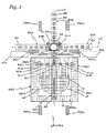
- FIG. 1 is a schematic view showing an exposure apparatus related to an embodiment
- FIG. 2 is a plan view showing a stage device in FIG. 1 ;
- FIG. 3 is a plan view showing the placement of various measurement devices (such as encoders, alignment systems, and a multipoint AF system) that are equipped in the exposure apparatus in FIG. 1 ;
- various measurement devices such as encoders, alignment systems, and a multipoint AF system
- FIG. 4A is a perspective view showing a configuration of a detection device in FIG. 3
- FIG. 4B is a view showing an incident state of a detection beam emitted from a light-transmitting system in FIG. 4 with respect to a scale;
- FIG. 5 is a block diagram showing a main configuration of a control system of the exposure apparatus related to the embodiment
- FIGS. 6A and 6B are views used to explain position measurement of a wafer stage within an XY plane by a plurality of encoders each including a plurality of heads placed in the array arrangement, and carryover of measurement values between the heads;
- FIG. 7A is a view showing an example of a configuration of an encoder
- FIG. 7B is a view showing the case where a laser beam LB having a sectional shape that is elongated in a periodic direction of a grating RG is used as a detection light;
- FIG. 8 is a view showing a state of the wafer stage and a measurement stage when exposure based on a step-and-scan method is being performed to a wafer on the wafer stage;
- FIG. 9 is a view showing a state of the wafer stage and the measurement stage when exposure to the wafer ends on the side of the wafer stage;
- FIG. 10 is a view showing a state of the wafer stage and the measurement stage immediately after the state of both stages goes from a state of separation to a state of coming into contact with each other;
- FIG. 11 is a view showing a state of the wafer stage and the measurement stage when the measurement stage moves to a ⁇ Y direction and the wafer stage moves toward an unloading position while keeping the positional relation between both stages in a Y-axis direction;
- FIG. 12 is a view showing a state of the wafer stage and the measurement stage when the measurement stage reaches a position where Sec-BCHK (interval) is performed;
- FIG. 13 is a view showing a state of the wafer stage and the measurement stage when the wafer stage moves from the unloading position to a loading position in parallel with the Sec-BCHK (interval) being performed;
- FIG. 14 is a view showing a state of the wafer stage and the measurement stage when the measurement stage moves to an optimal scrum waiting position and a wafer is loaded on the wafer stage;
- FIG. 15 is a view showing a state of the wafer stage and the measurement stage when the wafer stage moves to a position where the former process of Pri-BCHK is performed while the measurement stage is waiting at the optimal serum waiting position;
- FIG. 16 is a view showing a state of the wafer stage and the measurement stage when alignment marks arranged in three first alignment shot areas are simultaneously being detected using alignment system AL 1 , AL 2 2 and AL 2 3 ;
- FIG. 17 is a view showing a state of the wafer stage and the measurement stage when alignment marks arranged in five second alignment shot areas are simultaneously being detected using alignment system AL 1 , and AL 2 1 to AL 2 4 ;
- FIG. 18 is a view showing a state of the wafer stage and the measurement stage when alignment marks arranged in five third alignment shot areas are simultaneously being detected using alignment system AL 1 , and AL 2 2 , to AL 2 4 ;
- FIG. 19 is a view showing a state of the wafer stage and the measurement stage when alignment marks arranged in three fourth alignment shot areas are simultaneously being detected using alignment system AL 1 , AL 2 2 and AL 2 3 ;
- FIG. 20 is a view showing a state of the wafer stage and the measurement stage when focus mapping ends.
- FIG. 21 is a view showing a state of the wafer stage and the measurement stage during an exposure operation.
- FIG. 1 schematically shows a configuration of an exposure apparatus 100 related to the embodiment.
- Exposure apparatus 100 is a projection exposure apparatus based on a step-and-scan method, that is, a scanner.
- a projection optical system PL is arranged, and the following description will be made assuming that a direction parallel to an optical axis AX of projection optical system PL is a Z-axis direction, a direction in which a reticle and a wafer are relatively scanned within a plane orthogonal to the Z-axis direction is a Y-axis direction and a direction that is orthogonal to a Z-axis and a Y-axis is an X-axis direction, and rotation (tilt) directions around the X-axis, the Y-axis and the Z-axis are ⁇ x, ⁇ y and ⁇ z directions respectively.
- Exposure apparatus 100 is equipped with an illumination system 10 , a reticle stage RST that holds a reticle R that is illuminated by an illumination light for exposure (hereinafter, referred to as an “illumination light” or an “exposure light”) IL from illumination system 10 , a projection unit PU that includes projection optical system PL that projects illumination light IL emitted from reticle R on a wafer W, a stage device 50 that has a wafer stage WST and a measurement stage MST, their control system, and the like. On wafer stage WST, wafer W is mounted.
- Illumination system 10 includes a light source and an illumination optical system that has an illuminance uniformity optical system containing an optical integrator and the like, and a reticle blind and the like (none of which are shown), as is disclosed in, for example, Kokai (Japanese Unexamined Patent Application Publication) No. 2001-313250 (the corresponding U.S. Patent Application Publication No. 2003/0025890) and the like.
- illumination system 10 a slit-shaped illumination area IAR that is defined by the reticle blind (the masking system) on reticle R is illuminated by illumination light (exposure light) IL with substantially uniform illuminance.
- illumination light IL an ArF excimer laser light (wavelength: 193 nm) is used as an example.
- optical integrator for example, a fly-eye lens, a rod integrator (an internal reflection type integrator), a diffraction optical element or the like can be used.
- Reticle stage RST On reticle stage RST, reticle R having a pattern surface (the lower surface in FIG. 1 ) on which a circuit pattern and the like are formed is fixed by, for example, vacuum suction.
- Reticle stage RST is finely drivable within an XY plane and also drivable at designated scanning velocity in a scanning direction (which is the Y-axis direction being a lateral direction of the page surface of FIG. 1 ), by a reticle stage drive system 11 (not shown in FIG. 1 , refer to FIG. 5 ) including, for example, a linear motor or the like.
- Positional information of reticle stage RST is constantly measured by a reticle interferometer 116 .
- Projection unit PU is placed below reticle stage RST in FIG. 1 .
- Projection unit PU includes a barrel 40 and projection optical system PL having a plurality of optical elements that are held in a predetermined positional relation within barrel 40 .
- projection optical system PL for example, a dioptric system that is composed of a plurality of lenses (lens elements) that are disposed along optical axis AX direction parallel to the Z-axis direction is used.
- Projection optical system PL is, for example, both-side telecentric and has a predetermined projection magnification (e.g. one-quarter, one-fifth one-eighth times, or the like).
- illumination area IAR when illumination area IAR is illuminated by illumination light IL from illumination system 10 , illumination light IL having passed through reticle R whose pattern surface is placed substantially coincidentally with a first surface (an object plane) of projection optical system PL forms a reduced image of a circuit pattern (a reduced image of part of a circuit pattern) of reticle R within illumination area TAR on an area (hereinafter, also referred to as an “exposure area”) IA that is conjugate with illumination area IAR, on wafer W, which is placed on the second surface (the image plane) side of projection optical system PL and whose surface is coated with a resist (a photosensitive agent), via projection optical system PL (projection unit PU).
- exposure area an area that is conjugate with illumination area IAR, on wafer W, which is placed on the second surface (the image plane) side of projection optical system PL and whose surface is coated with a resist (a photosensitive agent), via projection optical system PL (projection unit PU).
- projection unit PU is mounted on a barrel platform that is supported by three support columns via a vibration isolation mechanism.
- the present invention is not limited thereto, and as is disclosed in, for example, the pamphlet of International Publication No. 2006/038952, projection unit PU may also be supported in a suspended state with respect to a main frame member (not shown) that is placed above projection unit PU, or a base member on which reticle stage RST is placed, or the like.
- a catadioptric system containing mirrors and lenses may also be used, in order to satisfy the Petzval condition and also avoid the increase in size of the projection optical system.
- a nozzle unit 32 that constitutes part of a local liquid immersion device 8 is arranged so as to enclose the periphery of the lower end portion of barrel 40 that holds an optical element closest to the image plane side (the wafer W side) that constitutes projection optical system PL, which is a lens (hereinafter, also referred to a “tip lens”) 191 in this case.
- the lower end surface of nozzle unit 32 is set substantially flush with the lower end surface of tip lens 191 .
- nozzle unit 32 is equipped with a supply opening and a recovery opening of a liquid Lq, a lower surface to which wafer W is placed opposing and at which the recovery opening is arranged, and a supply flow channel and a recovery flow channel that are connected to a liquid supply pipe 31 A and a liquid recovery pipe 31 B respectively.
- the liquid is supplied from a liquid supply device 5 (not shown in FIG. 1 , refer to FIG. 5 ) to the space between tip lens 191 and wafer W via liquid supply pipe 31 A, the supply flow channel and the supply opening, and the liquid is recovered from the space between tip lens 191 and wafer W by a liquid recovery device 6 (not shown in FIG. 1 , refer to FIG. 5 ) via the recovery opening, the recovery flow channel and liquid recovery pipe 31 B, so that a constant quantity of liquid Lq (refer to FIG. 2 ) is held in the space between tip lens 191 and wafer W. In this case, liquid Lq held in the space between tip lens 191 and wafer W is constantly replaced.
- pure water that transmits the ArF excimer laser light (the light with a wavelength of 193 nm) is to be used.
- Retractive index n of the water with respect to the ArF excimer laser light is around 1.44.
- the wavelength of illumination light IL is 193 nm ⁇ 1/n, shorted to around 134 nm.
- local liquid immersion device 8 is configured including nozzle unit 32 , liquid supply device 5 , liquid recovery device 6 , liquid supply pipe 31 A and liquid recovery pipe 31 S, and the like.
- part of local liquid immersion device 8 for example, at least nozzle unit 32 may also be supported in a suspended state by a main frame (including the barrel platform described above) that holds projection unit PU, or may also be arranged at another frame member that is separate from the main frame.
- nozzle unit 32 may also be supported in a suspended state integrally with projection unit PU, but in the embodiment, nozzle unit 32 is arranged at a measurement frame that is supported in a suspended state independently from projection unit PU. In this case, projection unit PU does not have to be supported in a suspended state
- the space between the measurement stage (to be described later) and tip lens 191 can be filled with water in the similar manner to the above-described manner.
- stage device 50 is equipped with wafer stage WST and measurement stage MST that are placed on a base board 12 , an interferometer system 118 (refer to FIG. 5 ) including Y-axis interferometers 16 and 18 that measure positional information of stages WST and MST, an encoder system 200 (refer to FIG. 5 ) that is used to measure positional information of wafer stage WST on exposure or the like, a stage drive system 124 (refer to FIG. 5 ) that drives stages WST and MST, detection devices PDX 1 to PDX 4 , PDY 1 and PDY 2 (to be described later, refer to the drawings such as FIGS. 3 and 5 ) and the like.
- an interferometer system 118 including Y-axis interferometers 16 and 18 that measure positional information of stages WST and MST
- an encoder system 200 (refer to FIG. 5 ) that is used to measure positional information of wafer stage WST on exposure or the like
- a stage drive system 124 (refer to
- a noncontact bearing (not shown), for example, a vacuum preload type hydrostatic air bearing (hereinafter, referred to as an “air pad”) is arranged at a plurality of positions.
- Wafer stage WST and measurement stage MST are supported in a noncontact manner via a clearance of around several ⁇ m above base board 12 , by static pressure of pressurized air that is blown out from the air pad toward the upper surface of base board 12 .
- stages WST and MST are drivable independently from each other at least in the Y-axis direction and the X-axis direction by stage drive system 124 .
- a wafer holder (not shown) that holds wafer W by vacuum suction or the like is arranged on wafer stage WST.
- the wafer holder may also be formed integrally with wafer stage WST, but in the embodiment, the wafer holder and wafer stage WST are separately configured, and the wafer holder is fixed inside a recessed portion of wafer stage WST, for example, by vacuum suction or the like.
- a plate (liquid repellent plate) 28 is arranged, which has the surface (the liquid repellent surface) substantially flush with the surface of a wafer mounted on the wafer holder to which liquid repellent treatment with respect to liquid Lq is applied, has a rectangular outer shape (contour), and has a circular opening that is formed in the center portion and is slightly larger than the wafer holder (a mounting area of the wafer).
- Plate 28 is made of materials with a low coefficient of thermal expansion, for example, glasses or ceramics (such as Zerodur (the brand name) of Schott AG, Al 2 O 3 , or TiC), and on the surface of plate 28 , a liquid repellent film is formed by, for example, fluorine resin materials, fluorine series resin materials such as polytetrafluoroethylene (Teflon®), acrylic series resin materials, silicon series resin materials, or the like. Further, as is shown in FIG.
- glasses or ceramics such as Zerodur (the brand name) of Schott AG, Al 2 O 3 , or TiC
- a liquid repellent film is formed by, for example, fluorine resin materials, fluorine series resin materials such as polytetrafluoroethylene (Teflon®), acrylic series resin materials, silicon series resin materials, or the like.
- plate 28 has a first liquid repellent area 28 a whose outer shape (contour) is rectangular enclosing the circular opening, and a second liquid repellent area 28 b that has a rectangular frame (loop) shape placed on the periphery of first liquid repellent area 28 a .
- first liquid repellent area 28 a for example, when an exposure operation is performed, at least part of a liquid immersion area 14 (e.g. refer to FIG. 3 ) protruding from the surface of the wafer is formed, and on second liquid repellent area 28 b , scales for the encoder system (to be described later) are formed.
- plate 28 does not have to be flush with the surface of the wafer, that is, may be different in height from the surface of the wafer.
- plate 28 may be a single plate, but in the embodiment, plate 28 is configured by combining a plurality of plates, for example, first and second liquid repellent plates that correspond to first liquid repellent area 28 a and second liquid repellent area 28 b respectively.
- first liquid repellent area 28 a and second liquid repellent area 28 b are also referred to as first water repellent plate 28 a and second water repellent plate 28 b respectively.
- exposure light IL is irradiated to first water repellent plate 28 a on the inner side, while exposure light IL is hardly irradiated to second water repellent plate 28 b on the outer side.
- a first water repellent area to which water repellent coat having sufficient resistance to exposure light IL (a light in a vacuum ultraviolet region, in this case) is applied is formed on the surface of first water repellent plate 28 a
- a second water repellent area to which water repellent coat having resistance to exposure light IL inferior to the first water repellent area is applied is formed on the surface of second water repellent plate 28 b .
- first water repellent plate 28 a and second water repellent plate 28 b On the periphery thereof.
- the present invention is not limited thereto, and two types of water repellent coat that have different resistance to exposure light IL may also be applied on the upper surface of the same plate in order to form the first water repellent area and the second water repellent area. Further, the same kind of water repellent coat may be applied to the first and second water repellent areas. For example, only one water repellent area may also be formed on the same plate.
- a rectangular cutout is formed in the center portion in the X-axis direction, and a measurement plate 30 is embedded inside the rectangular space (inside the cutout) that is enclosed by the cutout and second water repellent plate 28 b .
- a fiducial mark EM is formed in the center in the longitudinal direction of measurement plate 30 (on a centerline LL of wafer stage WST), and a pair of aerial image measurement slit patterns SL (slit-shaped measurement patterns) are formed in the symmetrical placement with respect to the center of fiducial mark FM on one side and the other side in the X-axis direction of fiducial mark FM.
- aerial image measurement slit patterns St an L-shaped slit pattern having sides along the Y-axis direction and X-axis direction, or two linear slit patterns extending in the X-axis direction and the Y-axis direction respectively can be used, as an example.
- an optical system and the like that constitute an aerial image measurement device 45 together with slit patterns SL are arranged.
- second water repellent plate 28 b is formed by two plate-shaped members 29 a and 29 b being stuck together.
- Y scales 39 Y 1 and 39 Y 2 are formed respectively.
- Each of Y scales 39 Y 1 and 39 Y 2 is configured of, for example, a reflective grating (e.g. a diffraction grating) having a periodic direction in the Y-axis direction, in which the grating lines having the longitudinal directions in the X-axis direction are formed in a predetermined pitch along a direction parallel to the Y-axis (the Y-axis direction).
- a reflective grating e.g. a diffraction grating
- the grating lines having the longitudinal directions in the X-axis direction are formed in a predetermined pitch along a direction parallel to the Y-axis (the Y-axis direction).
- X scales 39 X 1 and 39 X 2 are formed respectively.
- Each of X scales 39 X 1 and 39 X 2 is configured of, for example, a reflective grating (e.g. a diffraction grating) having a periodic direction in the X-axis direction, in which the grating lines having the longitudinal di reactions in the Y-axis direction are formed in a predetermined pitch along a direction parallel to the X-axis (the X-axis direction) in the embodiment, damage or the like of diffraction grating RG can be prevented because second water repellent plate 28 b is constituted by two plate-shaped members 29 a and 29 b as is described above and plate-shaped member 29 a on the upper side covers diffraction grating RG.
- the pitch of the grating is shown much wider in FIG. 2 than the actual pitch, for the sake of convenience. The same is true also in other drawings.
- Mirror finish is severally applied to the ⁇ Y end surface and the ⁇ X end surface of wafer stage WST, and a reflection surface 17 a and a reflection surface 17 b shown in FIG. 2 are formed.
- an interferometer beam (a measurement beam)
- Y-axis interferometer 16 and an X-axis interferometer 126 X-axis interferometer 126 is not shown in FIG. 1 , refer to FIG. 2 ) of interferometer system 118 (refer to FIG.
- Y-axis interferometer 16 and X-axis interferometer 126 a multiaxial interferometer having a plurality of measurement axes is used. Based on the measurement values of Y-axis interferometer 16 and X-axis interferometer 126 , main controller 20 can also measure rotational information in the ⁇ x direction (i.e. pitching), rotational information in the ⁇ y direction (i.e.
- positional information of wafer stage WST within the XY plane is mainly measured by each encoder of the encoder system (to be described later) that uses the Y scales and the X scales described above.
- the measurement values of interferometers 16 and 126 are secondarily used in the cases such as when long-term fluctuation of the measurement values of each encoder (e.g. due to deformation of the scales due to time passage, or the like) is corrected (calibrated).
- Y-axis interferometer 16 is used to measure the Y-position of wafer stage WST and the like in the vicinity of an unloading position and a loading position (to be described later) for wafer exchange. Further, also for movement of wafer stage WST, for example, between a loading operation and an alignment operation and/or between an exposure operation and an unloading operation, measurement information of interferometer system 118 , that is, at least one of positional information in directions of five degrees of freedom (the X-axis, Y-axis, ⁇ x, ⁇ y and ⁇ z directions) is used. Incidentally, at least part of interferometer system 118 (e.g.
- an optical system or the like may be arranged at the main frame that holds projection unit PU, or may also be arranged integrally with projection unit PU that is supported in a suspended state as is described above, but, in the embodiment, interferometer system 118 is to be arranged at the measurement frame described above.
- wafer stage WST a single stage that is movable in directions of six degrees of freedom is employed, but as wafer stage WST, a configuration may also be employed, which includes a stage main section that is freely movable within the XY plane and a water table that is mounted on the stage main section and is finely drivable in the Z-axis direction, the ⁇ x direction and ⁇ y direction relative to the stage main section. Further, instead of reflection surface 17 a and reflection surface 17 b , a movable mirror composed of a planar mirror may also be arranged at wafer stage WST.
- positional information of wafer stage WST is to be measured with a reflection surface of the fixed mirror arranged at projection unit PU serving as a reference surface, but the position where the reference surface is placed is not limited to projection unit PU, and positional information of wafer stage WST does not necessarily have to be measured using the fixed mirror.
- positional information of wafer stage WST measured by interferometer system 118 is not used in the exposure operation or the alignment operation (to be described later) but is to be used mainly in the calibration operation (i.e. calibration of measurement values) of each encoder or the like, but measurement information of interferometer system 118 (i.e. at least one of positional information in directions of five degrees of freedom) may also be used in, for example, the operations such as the exposure operation and/or the alignment operation.
- the encoder system measures positional information of wafer stage WST in directions of three degrees of freedom, that is, positional information in the X-axis, Y-axis and ⁇ z directions, using at least three encoders.
- Measurement stage MST has various types of measurement members and is drivable in directions of six degrees of freedom.
- the measurement members for example, as is shown in FIG. 2 , an uneven illuminance measuring sensor 94 that has a pinhole-shaped light-receiving section that receives illumination light IL on an image plane of projection optical system PL, an aerial image measuring instrument 96 that measures an aerial image (a projected image) of a pattern that is projected by projection optical system PL, and a wavefront aberration measuring instrument 98 based on the Shack-Hartman method that is disclosed in, for example, the pamphlet of International Publication No. 03/065428 and the like are employed.
- wavefront aberration measuring instrument 98 the one disclosed in, for example, the pamphlet of International Publication No. 99/60361 (the corresponding European Patent Application Publication No. 1 079 223) can also be used.
- measurement members are to be arranged at measurement stage MST in the embodiment, however, the types and/or the number of measurement members are/is not limited to them.
- measurement members for example, measurement members such as a transmittance measuring instrument that measures a transmittance of projection optical system PL, and/or a measuring instrument that observes local liquid immersion device 8 , for example, nozzle unit 32 (or tip lens 191 ) or the like may also be used.
- members different from the measurement members such as a cleaning member that cleans nozzle unit 32 , tip lens 191 or the like may also be mounted on measurement stage MST.
- an illuminance monitor that has a light-receiving section having a predetermined area size that receives illumination light IL on the image plane of projection optical system PL may also be employed, which is disclosed in, for example, Kokai (Japanese Unexamined Patent Application Publication) No. 11-016816 (the corresponding U.S. Patent Application Publication No. 2002/0061469) and the like, and this illuminance monitor is also preferably placed on the centerline.
- liquid immersion exposure is performed in which wafer W is exposed with exposure light (illumination light) IL via projection optical system PL and liquid (water) Lq, and accordingly uneven illuminance measuring sensor 94 (and the illuminance monitor), aerial image measuring instrument 96 and wavefront aberration measuring instrument 98 that are used in measurement using illumination light IL receive illumination light IL via projection optical system PL and water.
- uneven illuminance measuring sensor 94 and the illuminance monitor
- aerial image measuring instrument 96 and wavefront aberration measuring instrument 98 that are used in measurement using illumination light IL receive illumination light IL via projection optical system PL and water.
- the optical system or the like may be mounted on measurement stage MST, or the entire sensor may be placed on measurement stage MST.
- a plurality of reference marks M are formed as is shown in FIG. 2 .
- the plurality of reference marks M are formed in three-row arrays in the Y-axis direction in the same pitch, and the array of each row is formed being shifted from each other by a predetermined distance in the X-axis direction.
- a two-dimensional mark having a size that can be detected by the primary alignment system and secondary alignment systems (to be described later) is used.
- Reference mark M may also be different in shape (constitution) from fiducial mark FM described earlier, but in the embodiment, reference mark M and fiducial mark FM have the same constitution and also they have the same constitution with that of the alignment mark on wafer W.
- the surface of CD bar 46 and the surface of measurement stage MST (which may include the measurement members described above) are also covered with a liquid repellent film (a water repellent film) severally.
- secondary alignment systems AL 2 1 and AL 2 2 , and AL 2 3 and AL 2 4 whose detection centers are substantially symmetrically placed with respect to straight line LV are respectively arranged.
- five alignment systems AL 1 and AL 2 1 to AL 2 4 are fixed to the lower surface of the main frame that holds projection unit PU.
- the present invention is not limited thereto, and five alignment systems AL 1 and AL 2 1 to AL 2 4 may also be arranged, for example, at the measurement frame described above.
- Head units 62 A and 62 C are placed on the +X side and the ⁇ X side of projection unit PU respectively having the longitudinal direction in the X-axis direction, and also symmetrically with respect to optical axis AX of projection optical system PL at the same distance spaced apart from optical axis AX. Further, head units 62 B and 62 D are placed on the +Y side and the ⁇ Y side of projection unit PU respectively having the longitudinal direction in the Y-axis direction, and also at the same distance spaced apart from optical axis AX of projection optical system PL.
- each of head units 62 A and 62 C is equipped with a plurality (six in this case) of Y heads 64 that are placed at a predetermined distance on straight line LH that passes through optical axis AX of projection optical system PL along the X-axis direction and also is parallel with the X-axis.
- Head unit 62 A constitutes a multiple-lens (six-lens in this case) Y linear encoder (hereinafter, shortly referred to as a “Y encoder” or an “encoder” as needed) 70 A (refer to FIG. 5 ) that measures the position in the Y-axis direction (the Y-position) of wafer stage WST using Y scale 39 Y 1 described above.
- head unit 62 C constitutes a multiple-lens (six-lens in this case) Y linear encoder 70 C (refer to FIG. 5 ) that measures the Y-position of wafer stage WST using Y scale 39 Y 2 described above.
- a distance between adjacent Y heads 64 i.e. the measurement beams
- head units 62 A and 62 C is set shorter than a width of Y scales 39 Y 1 and 39 Y 2 described above in the X-axis direction (to be more preciser the length of the grating line).
- Head units 62 A and 62 C are equipped with six Z sensors 76 1 to 76 6 and 74 1 to 74 6 (not shown in FIG. 3 , refer to FIG. 5 ) respectively, which are arranged at the same X-positions as Y heads 64 equipped in head units 62 A and 62 C respectively but whose Y-positions are apart from Y heads 64 at a predetermined distance to the +Y side.
- Z sensors 74 1 to 74 6 and 76 1 to 76 6 are connected to main controller 20 via a processor (not shown).
- Z sensors 72 a to 72 d are also connected to main controller 20 via the processor.
- each Z sensor is equipped with a focus sensor, a sensor main section that houses the focus sensor and a drive section that drives the sensor main section in the Z-axis direction, and a measurement section that measures the displacement of the sensor main section in the Z-axis direction, and the like (none of which are shown).
- the focus sensor As the focus sensor, a displacement sensor based on an optical method similar to the optical pickup that optically reads the displacement of the surface subject to measurement by irradiating a detection beam to the surface subject to measurement and receiving the reflected light is used.
- the output signal of the focus sensor (which is also called focus error) is sent to the drive section.
- the drive section drives the sensor main section in the Z-axis direction so as to keep a distance between the sensor main section and the surface subject to measurement constant (to be more precise, so as to keep the surface subject to measurement at the best focus position of an optical system of the focus sensor). With this operation, the sensor main section follows the displacement of the surface subject to measurement in the Z-axis direction and the focus-lock state is maintained.
- the sensor main section in the focus-lock state, the sensor main section is displaced in the Z-axis direction so that a distance between the sensor main section and the surface subject to measurement is kept constant. Accordingly, by the encoder head of the measurement section measuring the displacement of the sensor main section in the Z-axis direction, the surface position (the Z-position) of the surface subject to measurement is measured.
- the measurement values of the encoder head of the measurement section are supplied to main controller 20 via the processor described above as the measurement values of the Z sensor.
- head unit 62 B is equipped with a plurality (seven in this case) of X heads 66 that are placed on straight line LV at a predetermined distance along the Y-axis direction.
- head unit 62 D is equipped with a plurality (eleven in this case, out of eleven X heads, however, three X heads that overlap primary alignment system AL 1 are not shown in FIG. 3 ) of X heads 66 that are placed on straight line LV at a predetermined distance.
- Head unit 623 constitutes a multiple-lens (seven-lens, in this case) X linear encoder (hereinafter, shortly referred to as an “X encoder” or an “encoder” as needed) 70 B (refer to FIG.
- X scale 39 X 1 and X head 66 facing X scale 39 X 1 may be used.
- X scale 39 X 2 and X head 66 facing X scale 39 X 2 may be used.
- X linear encoder 70 D is constituted by the X head 66 of head unit 62 D facing the X scale.
- a distance between adjacent X heads 66 i.e. measurement beams
- a distance between adjacent X heads 66 is set shorter than a width in the Y-axis direction of X scales 39 X 1 and 39 X 2 described above (to be more precise, the length of the grating line).
- X head 66 located innermost out of a plurality of X heads 66 that are equipped in each of head units 62 B and 62 D is fixed to the lower end portion of the barrel of projection optical system PL (to be more precise, to the side of nozzle unit 32 enclosing tip lens 191 ) so as to be placed as close as possible to the optical axis of projection optical system PL.
- Y heads 64 y 1 and 64 y 2 are respectively arranged, whose detection points are placed on a straight line parallel to the X-axis that passes through the detection center of primary alignment system AL 1 and are substantially symmetrically placed with respect to the detection center.
- the distance between Y heads 64 y 1 and 64 y 2 is set substantially equal to the distance between a pair of reference gratings 52 on CD bar 46 described previously.
- Y heads 64 y 1 and 64 y 2 face Y scales 39 y 2 and 39 y 1 respectively in the state show in FIG. 3 where the center of wafer W on wafer stage WST is on straight line LV.
- Y heads 64 y 1 and 64 y 2 face a pair of reference gratings 52 of CD bar 46 respectively, and the Y-position of CD bar 46 is measured at the position of each of reference gratings 52 by Y heads 64 y 1 and 64 y 2 facing the pair of reference gratings 52 .
- encoders that are constituted by Y heads 64 y 1 and 64 y 2 facing reference gratings 52 respectively are referred to as Y-axis linear encoders 70 E 2 and 70 F 2 .
- Y encoders 70 E 1 and 70 F 3 the Y encoders that are constituted by Y heads 64 y 1 and 64 y 2 that face Y scales 39 Y 2 and 39 Y 1 are referred to as Y encoders 70 E 1 and 70 F 3 .
- the measurement values of linear encoders 70 A to 70 F described above are supplied to main controller 20 , and main controller 20 controls the position of wafer stage WST within the XY plane based on the measurement values of linear encoders 70 A to 70 D, and also controls the rotation of CD bar 46 in the ⁇ z direction based on the measurement values of linear encoders 70 E and 70 F.
- FIG. 3 at exposure apparatus 100 (stage device 50 ) of the embodiment, six detection devices PDX 1 to PDX 4 , PDY 1 and PDY 2 (the hatching are drawn in FIG. 3 ) are arranged that are used to detect the surface state (e.g. the existence state of foreign substance or the like) of scales 39 X 1 , 39 X 2 , 39 Y 1 and 39 Y 2 , and a pair of reference gratings 52 on CD bar 46 .
- the surface state e.g. the existence state of foreign substance or the like
- Detection devices PDX 1 to PDX 4 , PDY 1 and PDY 2 may be supported in a suspended state by the main frame (including the barrel platform described above) that holds projection unit PU, or may be fixed to another frame member that is separate from the main frame.
- detection device PDX 1 is arranged at a position that is on the +Y side and on the ⁇ X side of projection unit PU
- detection device PDX 2 is arranged at a position that is on the +Y side and on the +X side of projection unit PU and is bilaterally-symmetric with detection device PDX 1 with reference to straight line LV
- detection device PDX 3 is arranged at a position that is on the ⁇ Y side and on the ⁇ X side of projection unit PU
- detection device PDX 1 is arranged at a position that is bilaterally-symmetric with detection device PDX 3 with reference to straight line LV.
- detection device PDY 1 is placed at a position that is on the ⁇ Y side of head unit 62 C and on the +Y side of an irradiation system 90 a (to be described later) r and detection device PDY 2 is placed at a position that is on the ⁇ Y side of head unit 62 A and on the +Y side of a photodetection system 90 b (to be described later) and is bilaterally-symmetric with detection device PDY 1 with reference to straight line LV.
- Detection device PDY 1 includes an irradiation system 69 A that irradiates a detection beam to the surface of scale 39 Y 2 and a photodetection system 69 B that receives the detection beam scattered at the surface of scale 39 Y 2 , as is shown in FIG. 4A .
- Irradiation system 69 A includes a light-transmitting section 61 including, for example, a laser light source, a collimator lens, an irradiation light adjusting member, an anomorphic prism, a diaphragm and the like, and a mirror 63 .
- the laser light source is a semiconductor laser that emits a detection beam having a wavelength of, for example, around 780 nm.
- the detection beam emitted from light-transmitting section 61 is reflected off mirror 63 and is incident on the surface of scale 39 Y 2 at an incident angle close to 90 degrees (89 degrees in FIG. 4 ). That is, the detection beam is incident substantially parallel to the surface of scale 39 Y 2 , and therefore, as is shown in FIG. 4B , the detection beam is irradiated to a band-shaped irradiation area BA that extends on the substantially entire area in the X-axis direction of the surface of scale 39 Y 2 . Then, in the case where a foreign substance (a particle) 11 exists on the surface of scale 39 Y 2 as is shown in FIG. 4A , the detection beam irradiated to foreign substance 11 is scattered
- Photodetection system 69 B includes a photodetection lens 65 and an image sensor 67 as is shown in FIG. 4A .
- image sensor 67 for example, a photoelectric detector such as a one-dimensional CCD (Charge-Coupled Device) or the like is used.
- CCD Charge-Coupled Device
- the detection beam from the detection device is irradiated to scales 39 X 1 , 39 X 2 , 39 Y 1 and 39 Y 2 and reference gratings 52 of CD bar 46 , there is the possibility that the diffracted light at the diffraction gratings of scales 39 X 1 , 39 X 2 , 39 Y 1 and 39 Y 2 and reference gratings 52 of CD bar 46 is received by photodetection system 69 S.
- a plurality of detection points of the multipoint AF system ( 90 a , 90 b ) are placed at a predetermined distance along the X-axis direction on the surface to be detected.
- the plurality of detection points are placed, for example, in the matrix arrangement having one row and M columns (M is a total number of detection points) or having two rows and N colas (N is a half of a total number of detection points).
- M is a total number of detection points
- N is a half of a total number of detection points.
- the plurality of detection points to which a detection beam is severally irradiated are not individually shown, but are shown as an elongate detection area AF that extends in the X-axis direction between irradiation system 90 a and photodetection system 90 b .
- the plurality of detection points are to be placed in one row and M columns, or two rows and N columns, but the number (s) of rows and/or columns is/are not limited to these numbers.
- the positions in the X-axis direction of detection points are preferably made to be different even between the different rows.
- the plurality of detection points are to be placed along the X-axis direction.
- the present invention is not limited to this, and all of or some of the plurality of detection points may also be placed at different positions in the Y-axis direction.
- the plurality of detection points may also be placed along a direction that intersects both of the X-axis and the Y-axis.
- X head 66 that measures the position in the X-axis direction of wafer stage WST is sequentially switched to adjacent X head 66 (e.g. X head 66 circled by a solid line is switched to X head 66 circled by a dotted line), and the measurement values are carried over before and after the switching.
- FIG. 7A shows one Y head 64 of head unit 62 A that irradiates a detection light (a measurement beam) to Y scale 39 Y 1 .
- Y head 64 is mainly configured of three sections, which are an irradiation system 64 a , an optical system 64 b and a photodetection system 64 c.
- Optical system 64 b is equipped with a polarization beam splitter PBS whose separation plane is parallel to an XZ plane, a pair of reflection mirrors: R 1 a and R 1 b , lenses L 2 a and L 2 b , quarter wavelength plates (hereinafter, referred to as ⁇ /4 plates) WP 1 a and WP 1 b , reflection mirrors R 2 a and R 2 b , and the like.
- Each of the polarization directions of the two beams that have reached polarization beam splitter PBS is rotated at an angle of 90 degrees with respect to the original direction. Therefore, the first-order diffracted beam of beam LB 1 that was previously transmitted through polarization beam splitter PBS is reflected off polarization beam splitter PBS and is incident on photodetection system 64 c , and also the first-order diffracted beam of beam LB 2 that was previously reflected off polarization beam splitter PBS is transmitted through polarization beam splitter PBS and is synthesized concentrically with the first-order diffracted beam of beam LB 1 and is incident on photodetection system 64 c.
- Y encoder 70 A since the optical path lengths of two beams to be interfered are extremely short and also are almost equal to each other, the influence by air fluctuations can mostly be ignored. Then, when Y scale 39 Y 1 (i.e. wafer stage WST) moves in the measurement direction (the Y-axis direction, in this case), the phase of each of the two beams changes and thus the intensity of the interference light changes. This change in the intensity of the interference light is detected by photodetection system 64 c , and positional information in accordance with the intensity change is output as the measurement value of Y encoder 70 A.
- Other encoders 70 B, 70 C, 70 D and the like are also configured similar to encoder 70 A.
- FIG. 8 shows a state where exposure based on a step-and-scan method is being performed to wafer W (in this case, to be a mid water of a certain lot (one lot containing 25 or 50 wafers), as an example) on wafer stage WST.
- main controller 20 controls the position within the XY plane (including the ⁇ z rotation) of wafer stage WST, based on the measurement values of at least three encoders out of two X heads 66 (X encoders 70 B and 70 D) indicated by being circled in FIG. 8 that face X scales 39 X 1 and 39 X 2 respectively and two Y heads 64 (Y encoders 70 A and 70 C) indicated by being circled in FIG.
- the Z sensors are placed also in the Y-axis direction inside or in the vicinity of head units 62 A and 62 C, and the position in the Z-axis direction, the ⁇ y rotation (rolling) and the ⁇ x rotation (pitching) of wafer stage WST may be controlled based on the measurement values of a plurality of the Z sensors. In either case, the control of the position in the Z-axis direction, the ⁇ y rotation and the ⁇ x rotation of wafer stage WST (focus leveling control of wafer W) during the exposure is performed based on the results of the focus mapping (to be described later) that was performed beforehand.
- the foregoing exposure operation is performed by main controller 20 repeating an inter-shot moving operation in which wafer stage WST is moved to a scanning starting position (accelerating starting position) for exposure of each shot area on wafer W based on the result of wafer alignment performed beforehand, for example, Enhanced Global Alignment (EGA which will be described later), the latest baselines of alignment systems AL 1 and AL 2 1 to AL 2 4 , and the like, and a scanning exposure operation in which a pattern formed on reticle R is transferred to each shot area by a scanning exposure method.
- EGA Enhanced Global Alignment
- the exposure operation described above is performed in a state where water is held in the space between tip lens 191 and wafer W.
- the exposure operation is performed in the order from the shot area located on the ⁇ Y side to the shot area located on the +Y side in FIG. 8 .
- Kokai Japanese Unexamined Patent Application Publication
- No. 61-044429 the corresponding U.S. Pat. No. 4,780,617
- some e.g.
- main controller 20 drives wafer stage WST and measurement stage MST simultaneously as is described above, water that is held in the space between tip lens 191 of projection unit PU and wafer W (water in liquid immersion area 14 ) sequentially moves from wafer W to plate 28 , CD bar 46 , and measurement stage MST, according to movement of wafer stage WST and measurement stage MST to the ⁇ Y side.
- the contact state (or proximity state) of wafer stage WST and measurement stage MST is maintained.
- FIG. 11 shows a state right before water in liquid immersion area 14 is delivered from plate 28 to CD bar 46 .
- main controller 20 switches the control of the Y-position and the ⁇ z rotation of wafer stage WST from the control based on the measurement values of Y encoders 70 A and 70 C to the control based on the measurement values of Y-axis interferometer 16 . Then, after a predetermined period of time, as is shown in FIG.
- main controller 20 stops measurement stage MST at this position, and also drives further wafer stage WST toward unloading position UP while measuring the X-position of wafer stage WST by X head 66 indicated by being circled in FIG. 12 that faces X scale 39 X 1 (X-linear encoder 703 B) and measuring the Y-position, the ⁇ z rotation and the like by Y-axis interferometer 16 , and stops wafer stage WST at unloading position UP.
- X head 66 indicated by being circled in FIG. 12 that faces X scale 39 X 1 (X-linear encoder 703 B) and measuring the Y-position, the ⁇ z rotation and the like by Y-axis interferometer 16 , and stops wafer stage WST at unloading position UP.
- water is held in the space between measurement stage MST and tip lens 191 .
- main controller 20 measures the relative positional relation (the baseline) of (the detection center of) secondary alignment system AL 2 n with reference to (the detection center of) primary alignment system AL 1 , using reference marks M of CD bar 46 .
- the baseline measurement in this case is performed at intervals of each wafer exchange, and thus hereinafter the baseline measurement is also described as “Sec-BCHK (interval)”.
- main controller 20 adjusts the ⁇ z rotation of CD bar 46 based on the measurement values of Y heads 64 y 1 and 64 y 2 that face a pair of reference gratings 52 on CD bar 46 respectively (Y-axis linear encoders 70 E 2 and 70 F 2 ), and also adjusts the XY-position of CD bar 46 using, for example, the measurement value of the interferometer, based on the measurement value of primary alignment system AL 1 that detects reference mark M that is located on centerline CL of measurement stage MST or in the vicinity thereof.
- main controller 20 obtains each of the baselines of four secondary alignment systems AL 2 1 to AL 2 4 by simultaneously measuring reference marks M on CD bar 46 within the fields of the respective secondary alignment systems using four secondary alignment systems AL 2 1 to AL 2 4 . And, when performing the subsequent process, drift of the baselines of four secondary alignment systems AL 2 1 to AL 2 4 are corrected by using the newly measured baselines.
- main controller 20 gives the command and makes a drive system of an unload arm (not shown) unload wafer W on wafer stage WST that stops at unloading position UP, and also drives wafer stage WST to the +X direction to move it to loading position LP.
- unload arm not shown
- main controller 20 moves measurement stage MST to an optimal waiting position (hereinafter, referred to as an “optimal scrum waiting position”) used to shift a state of measurement stage MST from a state of being away from wafer stage WST to the contact state (or proximity state) with wafer stage WST described previously.
- main controller 20 gives the command and makes a drive system of a load arm (not shown) load new wafer W onto wafer stage WST.
- FIG. 14 shows a state where wafer W is loaded on wafer stage WST.
- the above-described optimal scrum waiting position of measurement stage MST is appropriately set in accordance with the Y-coordinates of the alignment marks arranged in the alignment shot areas on the wafer.
- an operation of moving measurement stage MST to the optimal scrum waiting position that is needed on the sift to the contact state (or proximity state) described above becomes unnecessary, and therefore the number of movement of measurement stage MST can be reduced by one, compared with the case where measurement stage MST is made to wait at a position away from the optimal scrum waiting position.
- the optimal scrum waiting position is determined so that the shift to the contact state (or proximity state) described above can be performed at a position where wafer stage WST stops for the wafer alignment described earlier.
- main controller 20 moves wafer stage WST to the position shown in FIG. 15 .
- main controller 20 swatches control of the position of wafer stage WST within the XY plane from the control based on the measurement value of encoder 70 B regarding the X-axis direction and the measurement value of Y-axis interferometer 16 regarding the Y-axis direction and the ⁇ z rotation, to the control based on the measurement values of three encoders, which are either of two X heads 66 indicated by being circled in FIG. 15 that face X scales 39 X 1 and 39 X 2 (encoder 70 D) and two Y heads 64 y 2 and 64 y 1 indicated by being circled in FIG. 15 that face Y scales 39 Y 1 and 39 Y 2 (encoders 70 F 1 and 70 E 1 ).
- main controller 20 starts movement of wafer stage WST to the +Y direction, while controlling the position of wafer stage WST based on the measurement values of the three encoders described above. Then, when wafer stage WST reaches the position shown in FIG. 16 , main controller 20 makes wafer stage WST and measurement stage MST come into contact with each other (or be close to each other at a distance of around 300 ⁇ m), and immediately stops wafer stage WST.
- main controller 20 After the stop of wafer stage WST, main controller 20 almost simultaneously and individually detects the alignment marks (refer to star-shaped marks in FIG. 16 ) arranged in three shot areas (hereinafter, referred to as “first alignment shot areas”) using primary alignment system AL 1 and secondary alignment systems AL 2 2 and AL 2 3 , and links the detection results of three alignment systems AL 1 , AL 2 2 and AL 2 3 and the measurement values of the three encoders described above at the time of the detection and stores them in a memory (not shown).
- first alignment shot areas three shot areas
- the simultaneous detection of the alignment marks arranged in the three first alignment shot areas in this case is performed while changing the relative positional relation in the Z-axis direction (the focus direction) between a plurality of alignment systems AL 1 and AL 2 1 to AL 2 4 and wafer W mounted on wafer stage WST by changing the Z-position of wafer stage WST.
- the shift to the contact state (or proximity state) of measurement stage MST and wafer stage WST is completed at the position where detection of the alignment marks in the first alignment shot areas is performed, and from the position, the movement to the +Y direction of both stages WST and MST in the contact state (or proximity state) is started by main controller 20 .
- main controller 20 Prior to the start of the movement to the +Y direction of both stages WST and MST, as is shown in FIG. 16 , main controller 20 starts irradiation of detection beams from the multipoint AF system ( 90 a , 90 b ) to wafer stage WST. With this operation, the detection area of the multipoint AF system is formed on wafer stage WST.
- liquid immersion area 14 is formed near the boundary between CD bar 46 and wafer stage WST. That is, water in liquid immersion area 14 is in a state just before being delivered from CD bar 46 to wafer stage WST.
- main controller 20 almost simultaneously and individually detects the alignment marks (refer to star-shaped marks in FIG. 17 ) arranged in five shot areas (hereinafter, referred to as “second alignment shot areas”) located at positions that face alignment systems AL 1 and AL 2 1 to AL 2 4 respectively in FIG. 17 , using five alignment systems AL 1 and AL 2 1 to AL 2 4 , and links the detection results of five alignment systems AL 1 and AL 2 1 to AL 2 4 and the measurement values of the three encoders described above at the time of the detection, and then stores them in the memory (not shown).
- the simultaneous detection of the alignment marks arranged in the five second alignment shot areas in this case is also performed while changing the Z-position of wafer stage WST, similar to the detection of the first alignment shot areas.
- main controller 20 controls the position of wafer stage WST within the XY plane based on the measurement values of X head 66 that faces X scale 39 X 2 (X linear encoder 70 D) and Y linear encoders 70 E 1 and 70 F 1 .
- main controller 20 obtains the scaling (the shot magnification) of wafer W by, for example, performing a statistical computation based on the EGA method described above using the positional information, and based on the computed shot magnification main controller 20 may also adjust optical characteristics of projection optical system PL, for example, the projection magnification.
- optical characteristics of projection optical system PL are adjusted by controlling an adjustment device 68 (refer to FIG.
- main controller 20 may control adjustment device 68 so as to make adjustment device 68 adjust optical characteristics of projection optical system PL based on the detection results.
- the number of marks is not limited to eight, or to a half of the total number of marks subject to detection, but may be, for example, the number that is more than or equal to the number required for computation of the scaling of the wafer or the like.
- main controller 20 starts again movement to the +Y direction of both stages WST and MST in the contact state (or proximity state), and at the same time, starts the focus mapping (detection of positional information (surface position information) of the wafer W surface related to the Z-axis direction) using the multipoint AF system ( 90 a , 90 b )
- main controller 20 controls the position of wafer stage WST within the XY plane based on X head 66 that faces X scale 39 X 2 (X linear encoder 70 D) and two Y heads 64 y 2 and 64 y 1 that face Y scales 39 Y 1 and 39 Y 2 respectively (Y linear encoders 70 F 1 and 70 E 1 ).
- main controller 20 loads positional information (surface position information) of the wafer stage WST surface (the surface of plate 28 ) related to the Z-axis direction measured by the surface position sensor and positional information (surface position information) of the wafer W surface related to the Z-axis direction at a plurality of detection points detected by the multipoint AF system ( 90 a , 90 b ) at predetermined sampling intervals, while wafer stage WST proceeds to the +Y direction, and makes three pieces of information, which are two kinds of the loaded surface position information and the measurement values of Y linear encoders 70 F 1 and 70 E 1 at the time of each samplings correspond to one another and sequentially stores them in the memory (not shown).
- main controller 20 stops wafer stage WST at that position, and continues the movement of measurement stage MST to the +Y direction without stopping it.
- measurement stage MST reaches an exposure start waiting position where measurement stage MST waits until exposure is started on the side of wafer stage WST
- main controller 20 stops measurement stage MST at that position. Then, main controller 20 almost simultaneously and individually detects the alignment marks (refer to star-shaped marks in FIG.
- third alignment shot areas five shot areas (hereinafter, referred to as “third alignment shot areas”) that exist at positions that face alignment systems AL 1 and AL 2 1 to AL 2 4 in FIG. 18 , using five alignment systems AL 1 and AL 2 1 to AL 2 4 , links the detection results of five alignment systems AL 1 and AL 2 1 and AL 2 4 and the measurement values of three encoders 70 D, 70 F 1 and 70 E 1 at the time of the detection and stores them in the memory (not shown).
- the simultaneous detection of the alignment marks arranged in the five third alignment shot areas in this case is also performed while changing the Z-position of wafer stage WST, as is described above.
- main controller 20 starts movement of wafer stage WST to the +Y direction. Then, when wafer stage WST reaches the position shown in FIG. 19 , main controller 20 immediately stops wafer stage WST, and almost simultaneously and individually detects the alignment marks (refer to star-shaped marks in FIG. 19 ) arranged in three shot areas (hereinafter, referred to as “fourth alignment shot areas”) that f ace primary alignment system AL 1 and secondary alignment systems AL 2 2 and AL 2 3 respectively in the state of FIG. 19 , links the detection results of three alignment systems AL 1 , AL 2 2 and AL 2 3 and the measurement values of the three encoders described above at the time of the detection, and stores them in the memory (not shown).
- fourth alignment shot areas that f ace primary alignment system AL 1 and secondary alignment systems AL 2 2 and AL 2 3 respectively in the state of FIG. 19 , links the detection results of three alignment systems AL 1 , AL 2 2 and AL 2 3 and the measurement values of the three encoders described above at the time of the detection, and stores them in the memory
- the simultaneous detection of the alignment marks arranged in the three fourth alignment shot areas in this case is also performed while changing the Z-position of wafer stage WST, as is described above.
- the focus mapping is being continued.
- measurement stage MST is still waiting at the exposure start waiting position described above.
- main controller 20 performs a statistical computation, for example, based on the EGA method described above using the detection results of the 16 alignment marks in total obtained as described above and the corresponding measurement values of the four encoders, and computes alignment information (coordinate values) of all the shot areas on wafer W in an XY coordinate system that is defined by measurement axes of the four encoders.
- main controller 20 continues the focus mapping while moving wafer stage WST to the +Y direction again. Then, when the detection beam from the multipoint AF system ( 90 a , 90 b ) begins to be away from the wafer W surface, as is shown in FIG. 20 , main controller 20 ends the focus mapping. At this point in time, main controller 20 converts the surf ace position information regarding each detection point of the multipoint AF system ( 90 a , 90 b ) into data with reference to the surface position information by the surface position sensor that has been simultaneously loaded.
- main controller 20 performs exposure based on a step-and-scan method in a liquid immersion exposure method and sequentially transfers a reticle pattern on a plurality of shot areas on wafer W. This state is shown in FIG. 21 . Afterwards, the similar operations are repeatedly performed to the remaining wafers within the lot.
- the detection beam from irradiation system 69 A of detection device PDY 1 is irradiated at least once to the entire area in the Y-axis direction of scale 39 Y 2 . Accordingly, in the case where the scattered light is received by image sensor 67 that constitutes detection device PDY 1 , main controller 20 judges that a foreign substance exists on scale 39 Y 2 , and from the measurement result of encoder 70 C at the time of the detection, detects the Y-axis direction position (coordinate) of the foreign substance. Further, based on the detection result by image sensor 67 and the measurement result of encoder 70 B or 70 D, main controller 20 detects the position (coordinate) of the foreign substance on scale 39 Y 2 .
- the detection beam of detection device PDY 2 is also irradiated at least once to the entire area in the Y-axis direction of scale 39 Y 1 during the exposure operation similarly to the case of detection device PDY 1 , and therefore, in the case where the scattered light is received by image sensor 67 that constitutes detection device PDY 2 , main controller 20 judges that a foreign substance exists on scale 39 Y 1 , and from the measurement result of encoder 70 A at the time of the detection, detects the position (coordinate) of the foreign substance.
- main controller 20 executes judgment as to whether a foreign substance exists or not, and detection of the position (coordinate) of the foreign substance on scale 39 Y 1 .
- detection device PDX 1 or PDX 2 faces scale 39 X 1 , and during the exposure operation, the detection beam of detection device PDX 1 or PDX 2 is irradiated at least once to the entire surface area of scale 39 X 1 . Accordingly, main controller 20 executes judgment as to whether a foreign substance exists or not, and detection of the position (coordinate) of the foreign substance on scale 39 X 9 in the manner similar to the manner described above, using encoders 70 B and 70 A or 70 C and detection devices PDX 1 and PDX 2 .
- detection device PDX 3 or PDX 4 faces scale 39 X 2 , and either of the detection beam of detection device PDX 3 or the detection beam of detection device PDX 4 is irradiated at least once to the entire surface area of scale 39 X 2 , and therefore main controller 20 executes judgment as to whether a foreign substance exists or not, and detection of the position (coordinate) of the foreign substance on scale 39 X 2 using detection device PDX 3 or PDX 4 and encoders 70 D and Y-axis interferometer 16 .
- main controller 20 moves measurement stage MST to a position where reference grating 52 on CD bar 46 faces detection device PDX 1 or PDX 2 , and executes judgment as to whether a foreign substance exists on reference grating 52 or not, and detection of the position (coordinate) of the foreign substance on reference grating 52 using detection device PDX 1 or PDX 2 .
- the detection beam of detection device PDY 1 (PDY 2 ) is irradiated to the entire area of scale 39 Y 2 ( 39 Y 1 ) r and therefore, detection (inspection) of foreign substance on the upper sauce of scale 39 Y 2 ( 39 Y 1 ) may also be performed using detection device PDY 1 (PDY 2 ) during these operations. That is, the foreign substance detection operation may be carried out at least partially in parallel with another operation that is different from the exposure operation. Incidentally, the foreign substance detection operation may be carried out at least partially by itself. In this case, the placement and/or the number of the detection devices for foreign substance may be different from that/those in FIG. 3 .
- main controller 20 judges whether to perform cleaning (or replacement) of the scale or to continue the exposure operation (including the alignment operation and the like) in accordance with, for example, the operation status or the like, and in the case where the exposure operation (including the alignment operation and the like) is continued, the heads are selected avoiding the foreign substance so that the head that faces the foreign substance is not used during the operation.
- the heads that do not face the foreign substance are used by, for example, selecting the heads of three head units that do not face the foreign substance out of the four head units, or by changing the switching timing of heads in each head unit.
- an area where the foreign substance exists on the scale is identified as a non-measurement area to which measurement by encoder system 200 cannot be performed or with which measurement value becomes abnormal. Furthermore, in an operation in which position measurement of wafer stage WST by encoder system 200 is performed, for example, in the exposure operation, while selecting three encoder heads that do not face the non-measurement area according to the position of wafer stage WST, the position of wafer stage WST is controlled using the selected three encoder heads. Then, for example, at this stage, wafer stage WST is moved via stage drive system 124 , so that a portion where the foreign substance of the scale exits is located immediately below projection unit PU when exposure to wafer W mounted on wafer stage WST ends.
- main controller 20 returns wafer stage WST to the previous position and executes the continuation of the operation that has been performed partway.
- wafer stage WST is moved to unloading position UP to perform wafer exchange, and the exposure sequence is continued.
- the foreign substance removal is to be performed immediately after exposure of wafer W ends, but for example, when the exposure sequence ends, the foreign substance removal sequence may be carried out, that is, the foreign substance removal operation can be started.
- the non-measurement area of the scale identified from the foreign substance detection result may be only an area where the foreign substance exists but may also be an area larger than the foreign substance.
- main controller 20 immediately discontinues the exposure operation and performs the necessary process.
- the necessary process may be started when exposure of wafer W ends, without immediately stopping the exposure operation.
- whether or not the exposure operation can be carried out may be judged based on the foreign substance detection result.
- the judgment is made that the exposure operation can be carried out.
- the surface state of the scales (the existence state of foreign substance) is detected by irradiating the detection beam from irradiation system 69 A of detection devices PDX 1 to PDX 4 , PDY 1 and PDY 2 to scales 39 X 1 , 39 X 2 , 39 Y 1 and 39 Y 2 that are used to measure the position of wafer stage WST, and detecting the detection beam via scales 39 X 1 , 39 X 2 , 39 Y 1 and 39 Y 2 (scattered on scales 39 X 1 , 39 X 2 , 39 Y 1 and 39 Y 2 ) by photodetection system 69 B, and therefore detection of the surface state can be performed contactlessly with respect to the scales.
- the detection device can detect the surface state of the scales (the existence state of foreign substance), and therefore by performing position measurement of wafer stage WST using the scales taking the surface state into consideration, the highly precise position control of wafer stage WST can be performed.
- the detection device in the case where a foreign substance is found as a result of the detection of the detection device, the exposure operation is to be performed after the foreign substance is removed, and thus the highly precise position control of wafer stage WST can be performed without being affected by the foreign substance.
- the detection device also detects the surface state (the existence state of foreign substance) of reference gratings 52 on CD bar 46 , and therefore, the relative positional relation of (the detection center of) secondary alignment system AL 2 n with reference to (the detection center of) primary alignment system AL 1 can be detected with high accuracy, by performing the Sec-BCHK (interval) taking the surface state into consideration (such as removing the foreign substance). Besides, by performing exposure using this result, exposure with high precision can be achieved.
- the encoder system that includes encoders 70 A to 70 D and the like having good short term stability of measurement measures positional information of wafer stage WST within the XY plane, the measurement can be performed with high precision without being affected by air fluctuations or the like.
- the detection (the inspection) of foreign substance on the scale surface is to be performed in parallel with operations of exposure apparatus 100 such as the exposure operation, the alignment operation, or the wafer exchange operation being performed, but the present invention is not limited thereto.
- the foreign substance inspection of the scale surface may also be performed by moving wafer stage WST so that the detection beam of the detection device is irradiated to the entire area of the scale surface.
- the timing of the foreign substance inspection is not limited to each time when exposing one wafer as in the embodiment described above, but the foreign substance inspection may also be performed at each predetermined interval, such as each time when exposing a predetermined number of wafers or each time when a predetermined period of time lapses, or the foreign substance inspection may also be performed only when the instruction by a worker is made (when the entry to an input device (e.g. an inspection start button) of exposure apparatus 100 is made).
- the sequence may also be employed in which the detection (the inspection) of foreign substance is performed at each predetermined interval and the detection (the inspection) of foreign substance is also performed when the instruction by a worker is made.
- the sequence may also be employed in which the foreign substance inspection of part of the scales is performed when exposure to one wafer is performed and the foreign substance inspection of the reaming part of the scales is performed when exposure to the subsequent wafers is performed.
- the foreign substance in the case where a foreign substance exists on the scale surface, the foreign substance is to be removed (cleaned) using the liquid (the liquid used for liquid immersion exposure) of local liquid immersion device 8 , but the present invention is not limited thereto, and for example, the foreign substance may also be removed (cleaned) by supplying another liquid (cleaning liquid), which is different from the liquid used for liquid immersion exposure, from local liquid immersion device 8 and using another liquid.
- the cleaning liquid for example, a liquid having a higher oxygen concentration than liquid Lq (e.g. a liquid to which degassing treatment is not applied) may also be used.
- the cleaning may also be performed using, for example, a hydrogen peroxide solution.
- a hydrogen peroxide solution for example, optical cleaning by exposure light IL and/or ultrasonic cleaning may also be used in combination.
- a device similar to local liquid immersion device 8 is arranged at exposure apparatus 100 and by using such a device, the foreign substance on the scale may be removed. That is, a cleaning device (a foreign substance removal device) that is at least partially different from local liquid immersion device 8 may be arranged at another position that is separate from projection optical system PL (nozzle unit 32 ), for example, in a movement route of wafer stage WST between the exposure position where exposure light IL is irradiated via projection optical system PL and the water exchange position.
- a cleaning device a foreign substance removal device
- the present invention is not limited to the case where the foreign substance is removed using liquid, but an air-blow device that blows out air is arranged in exposure apparatus 100 and by using the air blown out from the air-blow device, the foreign substance on the scale surface may be removed. Further, a heating device that removes the foreign substance by heating it is arranged in exposure apparatus 100 , and by using the heating device, the foreign substance on the scale may be removed.
- main controller 20 may only issue a warning to a worker (an operator).
- the worker the operator
- the exposure apparatus may stop the exposure apparatus to perform the maintenance operation.
- the foreign substance removal operation may be performed (or the warning may be issued).
- the foreign substance removal operation may be performed or the warning may be issued.
- the present invention is not limited thereto, and the number of the detection devices may be any number as far as the detection beam can be irradiated to the entire areas of the scales.
- the placement of the detection devices is not limited to the placement of the embodiment described above as far as the detection beam can be irradiated to the entire area of the scales.
- an area to which foreign substance detection is performed may be the entire surface of the scale or may be only an area that is needed for position measurement of wafer stage WST.
- the foreign substance on the scale is dust or a water drop
- the foreign substance subject to detection of the detection devices is not limited to dust or a water drop.
- the encoder based on a diffraction interference method in which the light from the light source is branched by an optical element such as the beam splitter and which is equipped with two reflection mirrors that reflect the lights after being branched is to be used as encoders 70 A to 70 F, but the present invention is not limited thereto.
- head units 62 A to 62 D are to have a plurality of heads placed at a predetermined distance, but the present invention is not limited thereto, and a single head may also be employed that is equipped with a light source that emits a light beam to an area elongated in the pitch direction of the Y scale or the X scale, and many photodetection elements densely disposed in the pitch direction of the Y scale or the X scale that receive a reflected light (a diffracted light) of the light beam from (the diffraction grating of) the Y scale or the X scale.
- the X heads and the Y heads that is, one-dimensional heads are used as the encoder heads, but the present invention is not limited thereto, and a two-dimensional head (a 2D head) whose measurement directions are two orthogonal axes directions may also be used.
- a head integral with the Z sensor may be used as the encoder head. In the case of the integral head, a simple combination of the Z sensor and the encoder head may be employed, but a single sensor equipped with functions of the Z sensor and the encoder head may also be used as the encoder head.
- second water repellent plate 28 b is formed by two plate-shaped members 29 a and 29 b stuck together, but the present invention is not limited thereto, and second water repellent plate 28 b is composed of one plate-shaped member and the diffraction grating may be directly formed on its upper surface. Further, the diffraction grating is formed on the upper surface of second water repellent plate 28 b , and a protective member (e.g. a thin film) that can transmit the detection light from head units 62 A to 62 D is arranged on the upper surface of water repellent plate 28 b , so that damage of the diffraction grating may be prevented.
- a protective member e.g. a thin film
- the diffraction grating is directly formed on the wafer stage WST surface, and second water repellent plate 28 b may be arranged so as to cover the diffraction grating.
- a diffraction grating having narrow slits or grooves that are mechanically graved may also be employed, or for example, a diffraction grating that is created by exposing interference fringes on a photosensitive resin may also be employed.
- a reflective diffraction grating is to be arranged on the upper surface of wafer stage WST that is substantially parallel to the XY plane, but for example, the reflective diffraction grating may be arranged on the lower surface of wafer stage WST.
- head units 62 A to 62 D are placed on, for example, a base plate which the lower surface of wafer stage WST faces.
- an encoder system in which encoder heads are arranged on wafer stage WST and scales are arranged above wafer stage WST so as to face the encoder heads, may also be employed.
- Z sensors may also be placed on wafer stage WST and a predetermined surface (e.g. the surface) of the scale may be used also as a reflection surface that reflects measurement beams from the Z sensors.
- the detection devices described above are arranged at a movable body that is placed on base board 12 , and while moving the movable body, the foreign substance detection may be performed to the entire surface of the scale.
- the foreign substance removal device described above is also arranged at the movable body, and the foreign substance of the scale may be removed based on the foreign substance detection result.
- the movable body may be measurement stage MST, or may be provided separately from wafer stage WST and measurement stage MST.
- the detection devices and the foreign substance removal device described above may be mounted on different movable bodies.
- wafer stage WST is to be moved within a horizontal plane, but wafer stage WST may also be moved within a plane (e.g. a ZX plane) that intersects the horizontal plane. Further, the position of reticle stage RST may be measured by the encoder system.
- an encoder system having a configuration similar to the encoder system described above may also be arranged to measure positional information of reticle stage RST.
- the detection devices described above may also be used in order to detect a foreign substance on the scale (the diffraction grating) arranged on reticle stage RST. In either case, it is possible to detect a foreign substance on the scale by arranging the detection devices of the embodiment described above at the position facing the diffraction grating (the scale).
- a configuration of the detection device that detects a foreign substance is not limited to the configuration in the embodiment described above ( FIG. 4A ), but other configurations may also be employed as far as a detection device detects a foreign substance by irradiating the detection bean to the scale and receiving the detection beam via the scale.
- the multipoint AF system described above may also be used as the detection device, and in this case, the detection devices described above do not have to be provided separately from the multipoint AF system.
- the detection device may detect a foreign substance not only on the scale but also on the surface (the measurement surface) of the areas other than the area where wafer W is mounted on the upper surface of wafer stage WST.
- a foreign substance on the measurement surface can be detected by a detection device that is the same as or different from each of the detection devices of the embodiment described above, similarly to the case where a foreign substance on the scale is detected by each of the detection devices in the embodiment described above, which makes it possible to gain the effect equivalent to the embodiment described above.
- the lower surface of nozzle unit 32 and the lower end surface of the tip optical element of projection optical system PL are to be substantially flush.
- the present invention is not limited to thereto, and for example, the lower surface of nozzle unit 32 may also be placed closer to the image plane of projection optical system PL (i.e. to the wafer) than the outgoing surface of the tip optical element.
- the constitution of local liquid immersion device 8 is not limited to the above-described constitution, and the constitutions can be used, which are described in, for example, European Patent Application Publication No. 1 420 298, the pamphlet of International Publication No. 2004/055803, the pamphlet of International Publication No. 2004/057590, the pamphlet of International Publication No.
- the optical path on the object plane side of the tip optical element may also be filled with liquid, in addition to the optical path on the image plane side of the tip optical element.
- a thin film that is lyophilic and/or has dissolution preventing function may also be formed on the partial surface (including at least a contact surface with liquid) or the entire surface of the tip optical element.
- quartz has a high affinity for liquid, and also needs no dissolution preventing film, while in the case of fluorite, at least a dissolution preventing film is preferably formed.
- the recovered liquid may be reused, and in this case, a filter that removes impurities from the recovered liquid is preferably arranged in a liquid recovery device, a recovery pipe or the like.
- the exposure apparatus is a liquid immersion type exposure apparatus, but the present invention is not limited thereto and can also be employed in a dry type exposure apparatus that performs exposure of wafer W without liquid (water).
- the present invention is applied to the exposure apparatus that is equipped with all of water stage WST (a movable body), measurement sage MST (another movable body), the alignment systems (AL 1 , AL 2 1 to AL 2 4 ), the multipoint AF system ( 90 a , 90 b ), interferometer system 118 , encoder system 200 and the like, but the present invention is not limited thereto.
- the present invention can also be applied to an exposure apparatus in which measurement stage MST or the like is not arranged.
- both of the interferometer system and the encoder system do not always have to be arranged. That is, only the encoder system may be arranged.
- an alignment sensor which irradiates a coherent detection light to a subject mark and detects a scattered light or a diffracted light generated from the subject mark or makes two diffracted lights (e.g. diffracted lights of the same order or diffracted lights being diffracted in the same direction) generated from the subject mark interfere and detects an interference light, can naturally be used by itself or in combination as needed.
- alignment systems AL 1 and AL 2 1 to AL 2 4 are to be arranged in the embodiment described above, but the number of alignment systems is not limited to five, and may be the number more than or equal to two and less than or equal to four, or may be the number more than or equal to six, or may be the even number, not the odd number.
- one alignment system may be arranged, and alignment system (s) may be either movable or fixed.
- the present invention is applied to a scanning exposure apparatus based on a step-and-scan method or the like, but the present invention is not limited thereto, and may also be applied to a static exposure apparatus such as a stepper. Even with the stepper or the like, by measuring the position of a stage on which an object subject to exposure is mounted using encoders, occurrence of position measurement error caused by air fluctuations can substantially be nulled likewise.
- the present invention can also be applied to a reduced projection exposure apparatus based on a step-and-stitch method that synthesizes a shot area and a shot area, an exposure apparatus based on a proximity method, a mirror projection aligner, or the like.
- the present invention can also be applied to a multi-stage type exposure apparatus equipped with a plurality of wafer stages, as is disclosed in, for example, Kokai (Japanese Unexamined Patent Application Publications) No. 10-163099 and No. 10-214783 (the corresponding U.S. Pat. No. 6,590,634), Kohyo (published Japanese translation of International Publication for Patent Application) No. 2000-505958 (the corresponding U.S. Pat. No. 5,969,441), the U.S. Pat. No. 6,206,407, and the like.
- magnification of the projection optical system in the exposure apparatus in the embodiment described above is not only a reduction system, but also may be either an equal magnifying system or a magnifying system
- projection optical system PL is not only a dioptric system, but also may be either a catoptric system or a catadioptric system, and in addition, the projected image may be either an inverted image or an upright image.
- exposure area IA to which illumination light IL is irradiated via projection optical system PL is an on-axis area that includes optical axis AX within the field of projection optical system PL.
- the exposure area may also be an off-axis area that does not include optical axis AX, similar to a so-called inline type catadioptric system, in part of which an optical system (a catoptric system or a catadioptric system) that has a plurality of reflection surfaces and forms an intermediate image at least once is arranged, and which has a single optical axis.
- the illumination area and exposure area described above are to have a rectangular shape, but the shape is not limited to rectangular, and may also be circular arc, trapezoidal, parallelogram or the like.
- the light source of the exposure apparatus in the embodiment described above is not limited to the ArF excimer laser, but a pulsed laser light source such as a KrF excimer laser (output wavelength: 248 nm), an F 2 laser (output wavelength: 157 nm) an Ar 2 laser (output wavelength: 126 nm) or a Kr 2 laser (output wavelength: 146 nm), or an extra-high pressure mercury lamp that generates an emission line such as a g-line (wavelength: 436 nm) or an i-line (wavelength: 365 nm) can also be used. Further, a harmonic wave generation device of a YAG laser or the like can also be used.
- a pulsed laser light source such as a KrF excimer laser (output wavelength: 248 nm), an F 2 laser (output wavelength: 157 nm) an Ar 2 laser (output wavelength: 126 nm) or a Kr 2 laser (output wavelength: 146
- a harmonic wave which is obtained by amplifying a single-wavelength laser beam in the infrared or visible range emitted by a DFB semiconductor laser or fiber laser as vacuum ultraviolet light, with a fiber amplifier doped with, for example, erbium (or both erbium and ytteribium), and by converting the wavelength into ultraviolet light using a nonlinear optical crystal, may also be used.
- illumination light IL of the exposure apparatus is not limited to the light having a wavelength more than or equal to 100 nm, and it is needless to say that the light having a wavelength less than 100 nm may be used.
- an EUV exposure apparatus that makes an SOR or a plasma laser as a light source generate an EUV (Extreme Ultraviolet) light in a soft X-ray range (e.g. a wavelength range from 5 to 15 nm), and uses a total reflection reduction optical system designed under the exposure wavelength (e.g. 13.5 nm) and the reflective mask has been developed.
- EUV Extreme Ultraviolet
- the present invention can also be suitably applied to such an exposure apparatus.
- the present invention can also be applied to an exposure apparatus that uses charged particle beams such as an electron beam or an ion beam.
- a transmissive type mask which is a transmissive substrate on which a predetermined light shielding pattern (or a phase pattern or a light attenuation pattern) is formed, is used.
- a transmissive type mask which is a transmissive substrate on which a predetermined light shielding pattern (or a phase pattern or a light attenuation pattern) is formed.
- an electron mask which is also called a variable shaped mask, an active mask or an image generator, and includes, for example, a DMD (Digital Micromirror Device) that is a type of a non-emission type image display device (a spatial light modulator) or the like) on which a light-transmitting pattern, a reflection pattern, or an emission pattern is formed according to electronic data of the pattern that is to be exposed may also be used.
- a DMD Digital Micromirror Device
- a non-emission type image display device a spatial light modulator
- the present invention can also be applied to an exposure apparatus that synthesizes two reticle patterns on a wafer via a projection optical system and almost simultaneously performs double exposure of one shot area on the wafer by one scanning exposure, as is disclosed in, for example, Kohyo (published Japanese translation of International Publication for Patent Application) No. 2004-519850 (the corresponding U.S. Pat. No. 6,611,316).
- an apparatus that forms a pattern on an object is not limited to the exposure apparatus (the lithography system) described above, and for example, the present invention can also be applied to an apparatus that forms a pattern on an object based on an ink-jet method.
- an object or which a pattern should be formed is not limited to a wafer, but may be other objects such as a glass plate, a ceramic substrate, a film member, or a mask blank.
- the usage of the exposure apparatus is not limited to the exposure apparatus used for manufacturing semiconductor devices, but the present invention can be widely applied also to, for example, an exposure apparatus for manufacturing liquid crystal display devices which transfers a liquid crystal display device pattern onto a square-shaped glass plate, and to an exposure apparatus for manufacturing organic ELs, thin-film magnetic heads, imaging devices (such as CCDs), micromachines, DNA chips or the like. Further, the present invention can also be applied to an exposure apparatus that transfers a circuit pattern onto a glass substrate or a silicon wafer not only when producing microdevices such as semiconductor devices, but also when producing a reticle or a mask used in an exposure apparatus such as an optical exposure apparatus, an EUV exposure apparatus, an X-ray exposure apparatus, and an electron beam exposure apparatus.
- the exposure apparatus (the pattern formation apparatus) in the embodiment described above is manufactured by assembling various subsystems, which include the respective constituents that are recited in the claims of the present application, so as to keep predetermined mechanical accuracy, electrical accuracy and optical accuracy.
- a process of assembling various subsystems into the exposure apparatus includes mechanical connection, wiring connection of electric circuits, piping connection of pressure circuits, and the like among various types of subsystems. Needless to say, an assembly process of individual subsystem is performed before the process of assembling the various subsystems into the exposure apparatus.
- the making of the exposure apparatus is preferably performed in a clean room where the temperature, the degree of cleanliness and the like are controlled.
- Electron devices such as semiconductor devices are manufactured through the following steps: a step where the function/performance design of a device is performed; a step where a reticle based on the design step is manufactured; a step where a wafer is manufactured using materials such as silicon; a lithography step where a pattern of the mask (the reticle) is transferred onto the wafer by the exposure apparatus (the pattern formation apparatus) of the embodiment described above; a development step where the exposed wafer is developed; an etching step where an exposed member of an area other than the area where resist remains is removed by etching; a resist removing step where the resist that is no longer necessary when the etching is completed is removed; a device assembly step (including a dicing process, a bonding process, and a packaging process); an inspection step; and the like.
- the exposure method described above is executed using the exposure apparatus (the pattern formation apparatus) of the embodiment described above and device patterns are formed on the wafer, and therefore, highly-integrated devices can be manufactured
Landscapes
- Physics & Mathematics (AREA)
- General Physics & Mathematics (AREA)
- Epidemiology (AREA)
- Health & Medical Sciences (AREA)
- Public Health (AREA)
- Engineering & Computer Science (AREA)
- Environmental & Geological Engineering (AREA)
- Life Sciences & Earth Sciences (AREA)
- Atmospheric Sciences (AREA)
- Plasma & Fusion (AREA)
- Exposure And Positioning Against Photoresist Photosensitive Materials (AREA)
- Investigating Materials By The Use Of Optical Means Adapted For Particular Applications (AREA)
- Container, Conveyance, Adherence, Positioning, Of Wafer (AREA)
- Exposure Of Semiconductors, Excluding Electron Or Ion Beam Exposure (AREA)
- Length Measuring Devices By Optical Means (AREA)
Priority Applications (7)
| Application Number | Priority Date | Filing Date | Title |
|---|---|---|---|
| US12/128,036 US8098362B2 (en) | 2007-05-30 | 2008-05-28 | Detection device, movable body apparatus, pattern formation apparatus and pattern formation method, exposure apparatus and exposure method, and device manufacturing method |
| PCT/JP2008/060323 WO2008149913A1 (en) | 2007-05-30 | 2008-05-29 | Detection device, movable body apparatus, pattern formation apparatus and pattern formation method, exposure apparatus and exposure method, and device manufacturing method |
| KR1020097015554A KR20100028015A (ko) | 2007-05-30 | 2008-05-29 | 검출 디바이스, 이동체 장치, 패턴 형성 장치 및 패턴 형성 방법, 노광 장치 및 노광 방법, 및 디바이스 제조 방법 |
| JP2008140826A JP5169492B2 (ja) | 2007-05-30 | 2008-05-29 | 露光装置及び露光方法、並びにデバイス製造方法 |
| TW097120189A TWI413870B (zh) | 2007-05-30 | 2008-05-30 | Detection device, moving body device, pattern forming device and pattern forming method, exposure device and exposure method, and device manufacturing method |
| US13/324,334 US20120086927A1 (en) | 2007-05-30 | 2011-12-13 | Detection device, movable body apparatus, pattern formation apparatus and pattern formation method, exposure apparatus and exposure method, and device manufacturing method |
| JP2012183144A JP2012248888A (ja) | 2007-05-30 | 2012-08-22 | 検出装置、移動体装置、パターン形成装置及びパターン形成方法、露光装置、及びデバイス製造方法 |
Applications Claiming Priority (2)
| Application Number | Priority Date | Filing Date | Title |
|---|---|---|---|
| US92473607P | 2007-05-30 | 2007-05-30 | |
| US12/128,036 US8098362B2 (en) | 2007-05-30 | 2008-05-28 | Detection device, movable body apparatus, pattern formation apparatus and pattern formation method, exposure apparatus and exposure method, and device manufacturing method |
Related Child Applications (1)
| Application Number | Title | Priority Date | Filing Date |
|---|---|---|---|
| US13/324,334 Division US20120086927A1 (en) | 2007-05-30 | 2011-12-13 | Detection device, movable body apparatus, pattern formation apparatus and pattern formation method, exposure apparatus and exposure method, and device manufacturing method |
Publications (2)
| Publication Number | Publication Date |
|---|---|
| US20090004580A1 US20090004580A1 (en) | 2009-01-01 |
| US8098362B2 true US8098362B2 (en) | 2012-01-17 |
Family
ID=39720487
Family Applications (2)
| Application Number | Title | Priority Date | Filing Date |
|---|---|---|---|
| US12/128,036 Expired - Fee Related US8098362B2 (en) | 2007-05-30 | 2008-05-28 | Detection device, movable body apparatus, pattern formation apparatus and pattern formation method, exposure apparatus and exposure method, and device manufacturing method |
| US13/324,334 Abandoned US20120086927A1 (en) | 2007-05-30 | 2011-12-13 | Detection device, movable body apparatus, pattern formation apparatus and pattern formation method, exposure apparatus and exposure method, and device manufacturing method |
Family Applications After (1)
| Application Number | Title | Priority Date | Filing Date |
|---|---|---|---|
| US13/324,334 Abandoned US20120086927A1 (en) | 2007-05-30 | 2011-12-13 | Detection device, movable body apparatus, pattern formation apparatus and pattern formation method, exposure apparatus and exposure method, and device manufacturing method |
Country Status (5)
| Country | Link |
|---|---|
| US (2) | US8098362B2 (ja) |
| JP (1) | JP2012248888A (ja) |
| KR (1) | KR20100028015A (ja) |
| TW (1) | TWI413870B (ja) |
| WO (1) | WO2008149913A1 (ja) |
Cited By (2)
| Publication number | Priority date | Publication date | Assignee | Title |
|---|---|---|---|---|
| US9057485B2 (en) | 2009-05-01 | 2015-06-16 | Xtralis Technologies Ltd | Particle detectors |
| US9267884B2 (en) | 2008-06-10 | 2016-02-23 | Xtralis Technologies Ltd | Particle detection |
Families Citing this family (32)
| Publication number | Priority date | Publication date | Assignee | Title |
|---|---|---|---|---|
| US8237919B2 (en) * | 2007-08-24 | 2012-08-07 | Nikon Corporation | Movable body drive method and movable body drive system, pattern formation method and apparatus, exposure method and apparatus, and device manufacturing method for continuous position measurement of movable body before and after switching between sensor heads |
| SG183058A1 (en) * | 2007-12-17 | 2012-08-30 | Nikon Corp | Exposure apparatus, exposure method and device manufacturing method |
| NL1036618A1 (nl) * | 2008-03-24 | 2009-09-25 | Asml Netherlands Bv | Encoder-type measurement system, lithograpic apparatus and method to detect an error on or in a grid or grating of an encoder-type measurement system. |
| US8817236B2 (en) | 2008-05-13 | 2014-08-26 | Nikon Corporation | Movable body system, movable body drive method, pattern formation apparatus, pattern formation method, exposure apparatus, exposure method, and device manufacturing method |
| US8228482B2 (en) * | 2008-05-13 | 2012-07-24 | Nikon Corporation | Exposure apparatus, exposure method, and device manufacturing method |
| US8786829B2 (en) * | 2008-05-13 | 2014-07-22 | Nikon Corporation | Exposure apparatus, exposure method, and device manufacturing method |
| NL2003638A (en) * | 2008-12-03 | 2010-06-07 | Asml Netherlands Bv | Lithographic apparatus and device manufacturing method. |
| US8902402B2 (en) | 2008-12-19 | 2014-12-02 | Nikon Corporation | Movable body apparatus, exposure apparatus, exposure method, and device manufacturing method |
| US8773635B2 (en) * | 2008-12-19 | 2014-07-08 | Nikon Corporation | Exposure apparatus, exposure method, and device manufacturing method |
| US8760629B2 (en) | 2008-12-19 | 2014-06-24 | Nikon Corporation | Exposure apparatus including positional measurement system of movable body, exposure method of exposing object including measuring positional information of movable body, and device manufacturing method that includes exposure method of exposing object, including measuring positional information of movable body |
| US8599359B2 (en) | 2008-12-19 | 2013-12-03 | Nikon Corporation | Exposure apparatus, exposure method, device manufacturing method, and carrier method |
| NL2003845A (en) * | 2008-12-19 | 2010-06-22 | Asml Netherlands Bv | Lithographic apparatus, and patterning device for use in a lithographic process. |
| US8488109B2 (en) | 2009-08-25 | 2013-07-16 | Nikon Corporation | Exposure method, exposure apparatus, and device manufacturing method |
| US20110102761A1 (en) * | 2009-09-28 | 2011-05-05 | Nikon Corporation | Stage apparatus, exposure apparatus, and device fabricating method |
| US20110096312A1 (en) * | 2009-09-28 | 2011-04-28 | Nikon Corporation | Exposure apparatus and device fabricating method |
| US20110096306A1 (en) * | 2009-09-28 | 2011-04-28 | Nikon Corporation | Stage apparatus, exposure apparatus, driving method, exposing method, and device fabricating method |
| US20110096318A1 (en) * | 2009-09-28 | 2011-04-28 | Nikon Corporation | Exposure apparatus and device fabricating method |
| US20110123913A1 (en) * | 2009-11-19 | 2011-05-26 | Nikon Corporation | Exposure apparatus, exposing method, and device fabricating method |
| US20110128523A1 (en) * | 2009-11-19 | 2011-06-02 | Nikon Corporation | Stage apparatus, exposure apparatus, driving method, exposing method, and device fabricating method |
| US8488106B2 (en) * | 2009-12-28 | 2013-07-16 | Nikon Corporation | Movable body drive method, movable body apparatus, exposure method, exposure apparatus, and device manufacturing method |
| NL2006127A (en) * | 2010-02-17 | 2011-08-18 | Asml Netherlands Bv | A substrate table, a lithographic apparatus and a method for manufacturing a device using a lithographic apparatus. |
| US9207549B2 (en) | 2011-12-29 | 2015-12-08 | Nikon Corporation | Exposure apparatus and exposure method, and device manufacturing method with encoder of higher reliability for position measurement |
| RU2495372C1 (ru) * | 2012-03-21 | 2013-10-10 | Федеральное государственное бюджетное образовательное учреждение высшего профессионального образования "Московский государственный технологический университет "СТАНКИН" (ФГБОУ ВПО МГТУ "СТАНКИН") | Устройство для получения изображения микрорельефа объекта |
| JP6562707B2 (ja) * | 2015-05-13 | 2019-08-21 | キヤノン株式会社 | インプリント装置、インプリント方法及び物品の製造方法 |
| TWI582428B (zh) * | 2015-10-05 | 2017-05-11 | Pre - scan based track correction focusing leveling device and method | |
| CN105891215B (zh) * | 2016-03-31 | 2019-01-29 | 浙江工业大学 | 基于卷积神经网络的焊接视觉检测方法及装置 |
| JP7081490B2 (ja) * | 2016-09-27 | 2022-06-07 | 株式会社ニコン | レイアウト情報提供方法、レイアウト情報、決定方法、プログラム、並びに情報記録媒体 |
| JP6927690B2 (ja) * | 2016-11-04 | 2021-09-01 | 浜松ホトニクス株式会社 | 半導体デバイス検査装置及び半導体デバイス検査方法 |
| JP6517309B1 (ja) * | 2017-11-24 | 2019-05-22 | 浜松ホトニクス株式会社 | 異物除去方法、及び光検出装置の製造方法 |
| WO2020090075A1 (ja) * | 2018-10-31 | 2020-05-07 | 株式会社ニコン | 加工システム、及び、加工方法 |
| KR102221447B1 (ko) * | 2019-09-24 | 2021-03-02 | 주식회사 커미조아 | 판재결함 검출방법 및 장치 |
| CN113109349B (zh) * | 2021-03-23 | 2023-12-26 | 深圳中科飞测科技股份有限公司 | 检测方法、系统、设备及计算机可读存储介质 |
Citations (47)
| Publication number | Priority date | Publication date | Assignee | Title |
|---|---|---|---|---|
| JPS57117238A (en) | 1981-01-14 | 1982-07-21 | Nippon Kogaku Kk <Nikon> | Exposing and baking device for manufacturing integrated circuit with illuminometer |
| JPS6144429A (ja) | 1984-08-09 | 1986-03-04 | Nippon Kogaku Kk <Nikon> | 位置合わせ方法、及び位置合せ装置 |
| US4780617A (en) | 1984-08-09 | 1988-10-25 | Nippon Kogaku K.K. | Method for successive alignment of chip patterns on a substrate |
| JPH06283403A (ja) | 1993-03-26 | 1994-10-07 | Nikon Corp | 面位置設定装置 |
| US5448332A (en) | 1992-12-25 | 1995-09-05 | Nikon Corporation | Exposure method and apparatus |
| US5610715A (en) * | 1994-03-30 | 1997-03-11 | Canon Kabushiki Kaisha | Displacement detecting system, an expose apparatus, and a device manufacturing method employing a scale whose displacement is detected by a selected detection head |
| JPH10163099A (ja) | 1996-11-28 | 1998-06-19 | Nikon Corp | 露光方法及び露光装置 |
| JPH10214783A (ja) | 1996-11-28 | 1998-08-11 | Nikon Corp | 投影露光装置及び投影露光方法 |
| JPH1116816A (ja) | 1997-06-25 | 1999-01-22 | Nikon Corp | 投影露光装置、該装置を用いた露光方法、及び該装置を用いた回路デバイスの製造方法 |
| WO1999046835A1 (fr) | 1998-03-11 | 1999-09-16 | Nikon Corporation | Dispositif a laser ultraviolet et appareil d'exposition comportant un tel dispositif a laser ultraviolet |
| US5969441A (en) | 1996-12-24 | 1999-10-19 | Asm Lithography Bv | Two-dimensionally balanced positioning device with two object holders, and lithographic device provided with such a positioning device |
| WO1999060361A1 (fr) | 1998-05-19 | 1999-11-25 | Nikon Corporation | Instrument et procede de mesure d'aberrations, appareil et procede de sensibilisation par projection incorporant cet instrument, et procede de fabrication de dispositifs associe |
| US6208407B1 (en) | 1997-12-22 | 2001-03-27 | Asm Lithography B.V. | Method and apparatus for repetitively projecting a mask pattern on a substrate, using a time-saving height measurement |
| WO2001035168A1 (en) | 1999-11-10 | 2001-05-17 | Massachusetts Institute Of Technology | Interference lithography utilizing phase-locked scanning beams |
| JP2001313250A (ja) | 2000-02-25 | 2001-11-09 | Nikon Corp | 露光装置、その調整方法、及び前記露光装置を用いるデバイス製造方法 |
| JP2002014005A (ja) | 2000-04-25 | 2002-01-18 | Nikon Corp | 空間像計測方法、結像特性計測方法、空間像計測装置及び露光装置 |
| US20020041377A1 (en) | 2000-04-25 | 2002-04-11 | Nikon Corporation | Aerial image measurement method and unit, optical properties measurement method and unit, adjustment method of projection optical system, exposure method and apparatus, making method of exposure apparatus, and device manufacturing method |
| JP2003028673A (ja) | 2001-07-10 | 2003-01-29 | Canon Inc | 光学式エンコーダ、半導体製造装置、デバイス製造方法、半導体製造工場および半導体製造装置の保守方法 |
| US20030025890A1 (en) | 2000-02-25 | 2003-02-06 | Nikon Corporation | Exposure apparatus and exposure method capable of controlling illumination distribution |
| US6590634B1 (en) | 1996-11-28 | 2003-07-08 | Nikon Corporation | Exposure apparatus and method |
| WO2003065428A1 (fr) | 2002-01-29 | 2003-08-07 | Nikon Corporation | Systeme de reglage d'etat de formation d'images, procede d'insolation, appareil d'exposition, programme, et support d'enregistrement d'information |
| US6611316B2 (en) | 2001-02-27 | 2003-08-26 | Asml Holding N.V. | Method and system for dual reticle image exposure |
| US6639686B1 (en) | 2000-04-13 | 2003-10-28 | Nanowave, Inc. | Method of and apparatus for real-time continual nanometer scale position measurement by beam probing as by laser beams and the like of atomic and other undulating surfaces such as gratings or the like relatively moving with respect to the probing beams |
| WO2004019128A2 (en) | 2002-08-23 | 2004-03-04 | Nikon Corporation | Projection optical system and method for photolithography and exposure apparatus and method using same |
| EP1420298A2 (en) | 2002-11-12 | 2004-05-19 | ASML Netherlands B.V. | Immersion lithographic apparatus and device manufacturing method |
| WO2004055801A1 (ja) | 2002-12-17 | 2004-07-01 | Matsushita Electric Industrial Co., Ltd. | 光記録媒体および光記録方法 |
| WO2004057590A1 (en) | 2002-12-19 | 2004-07-08 | Koninklijke Philips Electronics N.V. | Method and device for irradiating spots on a layer |
| US6778257B2 (en) | 2001-07-24 | 2004-08-17 | Asml Netherlands B.V. | Imaging apparatus |
| WO2004086468A1 (ja) | 2003-02-26 | 2004-10-07 | Nikon Corporation | 露光装置、露光方法及びデバイス製造方法 |
| JP2004289126A (ja) | 2002-11-12 | 2004-10-14 | Asml Netherlands Bv | リソグラフィ装置およびデバイス製造方法 |
| WO2004107011A1 (ja) | 2003-05-06 | 2004-12-09 | Nikon Corporation | 投影光学系、露光装置及び露光方法 |
| WO2005029559A1 (ja) | 2003-09-19 | 2005-03-31 | Nikon Corporation | 露光装置及びデバイス製造方法 |
| JP2005114406A (ja) | 2003-10-03 | 2005-04-28 | Sendai Nikon:Kk | 光学式エンコーダ |
| US20050168714A1 (en) | 2004-02-03 | 2005-08-04 | Asml Netherlands B. V. | Lithographic apparatus, measurement system, and device manufacturing method |
| US20050206887A1 (en) * | 1991-04-02 | 2005-09-22 | Hiroshi Morioka | Method and apparatus for analyzing the state of generation of foreign particles in semiconductor fabrication process |
| US20060007419A1 (en) | 2004-07-07 | 2006-01-12 | Asml Netherlands B.V. | Lithographic apparatus and device manufacturing method |
| WO2006038952A2 (en) | 2004-09-30 | 2006-04-13 | Nikon Corporation | Projection optical device and exposure apparatus |
| US20060227309A1 (en) | 2005-04-08 | 2006-10-12 | Asml Netherlands B.V. | Lithographic apparatus and device manufacturing method |
| US20070052976A1 (en) | 2005-09-02 | 2007-03-08 | Asml Netherlands B.V. | Position measurement system and lithographic apparatus |
| EP1783822A1 (en) | 2004-06-21 | 2007-05-09 | Nikon Corporation | Exposure device, exposure device member cleaning method, exposure device maintenance method, maintenance device, and device manufacturing method |
| WO2007097379A1 (ja) | 2006-02-21 | 2007-08-30 | Nikon Corporation | パターン形成装置、マーク検出装置、露光装置、パターン形成方法、露光方法及びデバイス製造方法 |
| US20070263191A1 (en) | 2006-02-21 | 2007-11-15 | Nikon Corporation | Pattern forming apparatus and pattern forming method, movable member drive system and movable member drive method, exposure apparatus and exposure method, and device manufacturing method |
| US20070263197A1 (en) | 2006-05-09 | 2007-11-15 | Asml Nethlerlands B.V. | Displacement measurement system, lithographic apparatus, displacement measurement method and device manufacturing method |
| US20070285631A1 (en) * | 2006-05-22 | 2007-12-13 | Asml Netherland B.V | Lithographic apparatus and lithographic apparatus cleaning method |
| US20070288121A1 (en) | 2006-01-19 | 2007-12-13 | Nikon Corporation | Movable body drive method, movable body drive system, pattern formation method, pattern forming apparatus, exposure method, exposure apparatus, and device manufacturing method |
| US20080008843A1 (en) | 2006-03-02 | 2008-01-10 | Fred Ratel | Method for Production of Metal Oxide Coatings |
| US20080043212A1 (en) | 2006-02-21 | 2008-02-21 | Nikon Corporation | Measuring apparatus and method, processing apparatus and method, pattern forming apparatus and method, exposure apparatus and method, and device manufacturing method |
Family Cites Families (8)
| Publication number | Priority date | Publication date | Assignee | Title |
|---|---|---|---|---|
| JP3339856B2 (ja) * | 1990-04-02 | 2002-10-28 | 株式会社日立製作所 | 異物検出方法及びそれを用いた半導体装置製造方法 |
| JP3050431B2 (ja) * | 1990-10-02 | 2000-06-12 | 日立電子エンジニアリング株式会社 | 面板異物検査装置 |
| JP3126546B2 (ja) * | 1992-04-27 | 2001-01-22 | キヤノン株式会社 | 検査装置と検査方法、並びにこれを用いたシステム |
| US5877897A (en) * | 1993-02-26 | 1999-03-02 | Donnelly Corporation | Automatic rearview mirror, vehicle lighting control and vehicle interior monitoring system using a photosensor array |
| JPH11344361A (ja) * | 1998-06-03 | 1999-12-14 | Olympus Optical Co Ltd | 光学式エンコーダ |
| US7317504B2 (en) * | 2004-04-08 | 2008-01-08 | Asml Netherlands B.V. | Lithographic apparatus and device manufacturing method |
| JP4677833B2 (ja) * | 2004-06-21 | 2011-04-27 | 株式会社ニコン | 露光装置、及びその部材の洗浄方法、露光装置のメンテナンス方法、メンテナンス機器、並びにデバイス製造方法 |
| JP5353005B2 (ja) * | 2005-07-11 | 2013-11-27 | 株式会社ニコン | 露光装置、露光方法、及びデバイス製造方法 |
-
2008
- 2008-05-28 US US12/128,036 patent/US8098362B2/en not_active Expired - Fee Related
- 2008-05-29 KR KR1020097015554A patent/KR20100028015A/ko not_active Application Discontinuation
- 2008-05-29 WO PCT/JP2008/060323 patent/WO2008149913A1/en active Application Filing
- 2008-05-30 TW TW097120189A patent/TWI413870B/zh not_active IP Right Cessation
-
2011
- 2011-12-13 US US13/324,334 patent/US20120086927A1/en not_active Abandoned
-
2012
- 2012-08-22 JP JP2012183144A patent/JP2012248888A/ja active Pending
Patent Citations (59)
| Publication number | Priority date | Publication date | Assignee | Title |
|---|---|---|---|---|
| JPS57117238A (en) | 1981-01-14 | 1982-07-21 | Nippon Kogaku Kk <Nikon> | Exposing and baking device for manufacturing integrated circuit with illuminometer |
| US4465368A (en) | 1981-01-14 | 1984-08-14 | Nippon Kogaku K.K. | Exposure apparatus for production of integrated circuit |
| JPS6144429A (ja) | 1984-08-09 | 1986-03-04 | Nippon Kogaku Kk <Nikon> | 位置合わせ方法、及び位置合せ装置 |
| US4780617A (en) | 1984-08-09 | 1988-10-25 | Nippon Kogaku K.K. | Method for successive alignment of chip patterns on a substrate |
| US20050206887A1 (en) * | 1991-04-02 | 2005-09-22 | Hiroshi Morioka | Method and apparatus for analyzing the state of generation of foreign particles in semiconductor fabrication process |
| US5448332A (en) | 1992-12-25 | 1995-09-05 | Nikon Corporation | Exposure method and apparatus |
| JPH06283403A (ja) | 1993-03-26 | 1994-10-07 | Nikon Corp | 面位置設定装置 |
| US5610715A (en) * | 1994-03-30 | 1997-03-11 | Canon Kabushiki Kaisha | Displacement detecting system, an expose apparatus, and a device manufacturing method employing a scale whose displacement is detected by a selected detection head |
| JPH10214783A (ja) | 1996-11-28 | 1998-08-11 | Nikon Corp | 投影露光装置及び投影露光方法 |
| US6590634B1 (en) | 1996-11-28 | 2003-07-08 | Nikon Corporation | Exposure apparatus and method |
| JPH10163099A (ja) | 1996-11-28 | 1998-06-19 | Nikon Corp | 露光方法及び露光装置 |
| US5969441A (en) | 1996-12-24 | 1999-10-19 | Asm Lithography Bv | Two-dimensionally balanced positioning device with two object holders, and lithographic device provided with such a positioning device |
| JP2000505958A (ja) | 1996-12-24 | 2000-05-16 | コーニンクレッカ フィリップス エレクトロニクス エヌ ヴィ | 2個の物品ホルダを有する二次元バランス位置決め装置及びこの位置決め装置を有するリソグラフ装置 |
| JPH1116816A (ja) | 1997-06-25 | 1999-01-22 | Nikon Corp | 投影露光装置、該装置を用いた露光方法、及び該装置を用いた回路デバイスの製造方法 |
| US20020061469A1 (en) | 1997-06-25 | 2002-05-23 | Nikon Corporation | Projection apparatus, method of manufacturing the apparatus,method of exposure using the apparatus, and method of manufacturing circuit devices by using the apparatus |
| US6208407B1 (en) | 1997-12-22 | 2001-03-27 | Asm Lithography B.V. | Method and apparatus for repetitively projecting a mask pattern on a substrate, using a time-saving height measurement |
| US7023610B2 (en) | 1998-03-11 | 2006-04-04 | Nikon Corporation | Ultraviolet laser apparatus and exposure apparatus using same |
| WO1999046835A1 (fr) | 1998-03-11 | 1999-09-16 | Nikon Corporation | Dispositif a laser ultraviolet et appareil d'exposition comportant un tel dispositif a laser ultraviolet |
| EP1079223A1 (en) | 1998-05-19 | 2001-02-28 | Nikon Corporation | Aberration measuring instrument and measuring method, projection exposure apparatus provided with the instrument and device-manufacturing method using the measuring method, and exposure method |
| WO1999060361A1 (fr) | 1998-05-19 | 1999-11-25 | Nikon Corporation | Instrument et procede de mesure d'aberrations, appareil et procede de sensibilisation par projection incorporant cet instrument, et procede de fabrication de dispositifs associe |
| WO2001035168A1 (en) | 1999-11-10 | 2001-05-17 | Massachusetts Institute Of Technology | Interference lithography utilizing phase-locked scanning beams |
| US20030025890A1 (en) | 2000-02-25 | 2003-02-06 | Nikon Corporation | Exposure apparatus and exposure method capable of controlling illumination distribution |
| JP2001313250A (ja) | 2000-02-25 | 2001-11-09 | Nikon Corp | 露光装置、その調整方法、及び前記露光装置を用いるデバイス製造方法 |
| US6639686B1 (en) | 2000-04-13 | 2003-10-28 | Nanowave, Inc. | Method of and apparatus for real-time continual nanometer scale position measurement by beam probing as by laser beams and the like of atomic and other undulating surfaces such as gratings or the like relatively moving with respect to the probing beams |
| US20020041377A1 (en) | 2000-04-25 | 2002-04-11 | Nikon Corporation | Aerial image measurement method and unit, optical properties measurement method and unit, adjustment method of projection optical system, exposure method and apparatus, making method of exposure apparatus, and device manufacturing method |
| JP2002014005A (ja) | 2000-04-25 | 2002-01-18 | Nikon Corp | 空間像計測方法、結像特性計測方法、空間像計測装置及び露光装置 |
| US6611316B2 (en) | 2001-02-27 | 2003-08-26 | Asml Holding N.V. | Method and system for dual reticle image exposure |
| JP2004519850A (ja) | 2001-02-27 | 2004-07-02 | エイエスエムエル ユーエス, インコーポレイテッド | デュアルレチクルイメージを露光する方法および装置 |
| JP2003028673A (ja) | 2001-07-10 | 2003-01-29 | Canon Inc | 光学式エンコーダ、半導体製造装置、デバイス製造方法、半導体製造工場および半導体製造装置の保守方法 |
| US6778257B2 (en) | 2001-07-24 | 2004-08-17 | Asml Netherlands B.V. | Imaging apparatus |
| WO2003065428A1 (fr) | 2002-01-29 | 2003-08-07 | Nikon Corporation | Systeme de reglage d'etat de formation d'images, procede d'insolation, appareil d'exposition, programme, et support d'enregistrement d'information |
| WO2004019128A2 (en) | 2002-08-23 | 2004-03-04 | Nikon Corporation | Projection optical system and method for photolithography and exposure apparatus and method using same |
| US20050248856A1 (en) | 2002-08-23 | 2005-11-10 | Nikon Corporation | Projection optical system and method for photolithography and exposure apparatus and method using same |
| EP1420298A2 (en) | 2002-11-12 | 2004-05-19 | ASML Netherlands B.V. | Immersion lithographic apparatus and device manufacturing method |
| JP2004289126A (ja) | 2002-11-12 | 2004-10-14 | Asml Netherlands Bv | リソグラフィ装置およびデバイス製造方法 |
| US6952253B2 (en) | 2002-11-12 | 2005-10-04 | Asml Netherlands B.V. | Lithographic apparatus and device manufacturing method |
| WO2004055801A1 (ja) | 2002-12-17 | 2004-07-01 | Matsushita Electric Industrial Co., Ltd. | 光記録媒体および光記録方法 |
| WO2004057590A1 (en) | 2002-12-19 | 2004-07-08 | Koninklijke Philips Electronics N.V. | Method and device for irradiating spots on a layer |
| WO2004086468A1 (ja) | 2003-02-26 | 2004-10-07 | Nikon Corporation | 露光装置、露光方法及びデバイス製造方法 |
| US20050280791A1 (en) | 2003-02-26 | 2005-12-22 | Nikon Corporation | Exposure apparatus, exposure method, and method for producing device |
| EP1630585A1 (en) | 2003-05-06 | 2006-03-01 | Nikon Corporation | Projection optical system, and exposure apparatus and exposure method |
| WO2004107011A1 (ja) | 2003-05-06 | 2004-12-09 | Nikon Corporation | 投影光学系、露光装置及び露光方法 |
| WO2005029559A1 (ja) | 2003-09-19 | 2005-03-31 | Nikon Corporation | 露光装置及びデバイス製造方法 |
| US20060231206A1 (en) | 2003-09-19 | 2006-10-19 | Nikon Corporation | Exposure apparatus and device manufacturing method |
| JP2005114406A (ja) | 2003-10-03 | 2005-04-28 | Sendai Nikon:Kk | 光学式エンコーダ |
| US20050168714A1 (en) | 2004-02-03 | 2005-08-04 | Asml Netherlands B. V. | Lithographic apparatus, measurement system, and device manufacturing method |
| EP1783822A1 (en) | 2004-06-21 | 2007-05-09 | Nikon Corporation | Exposure device, exposure device member cleaning method, exposure device maintenance method, maintenance device, and device manufacturing method |
| US20060007419A1 (en) | 2004-07-07 | 2006-01-12 | Asml Netherlands B.V. | Lithographic apparatus and device manufacturing method |
| WO2006038952A2 (en) | 2004-09-30 | 2006-04-13 | Nikon Corporation | Projection optical device and exposure apparatus |
| US20060227309A1 (en) | 2005-04-08 | 2006-10-12 | Asml Netherlands B.V. | Lithographic apparatus and device manufacturing method |
| US20070052976A1 (en) | 2005-09-02 | 2007-03-08 | Asml Netherlands B.V. | Position measurement system and lithographic apparatus |
| US20070288121A1 (en) | 2006-01-19 | 2007-12-13 | Nikon Corporation | Movable body drive method, movable body drive system, pattern formation method, pattern forming apparatus, exposure method, exposure apparatus, and device manufacturing method |
| WO2007097379A1 (ja) | 2006-02-21 | 2007-08-30 | Nikon Corporation | パターン形成装置、マーク検出装置、露光装置、パターン形成方法、露光方法及びデバイス製造方法 |
| US20070263191A1 (en) | 2006-02-21 | 2007-11-15 | Nikon Corporation | Pattern forming apparatus and pattern forming method, movable member drive system and movable member drive method, exposure apparatus and exposure method, and device manufacturing method |
| US20080043212A1 (en) | 2006-02-21 | 2008-02-21 | Nikon Corporation | Measuring apparatus and method, processing apparatus and method, pattern forming apparatus and method, exposure apparatus and method, and device manufacturing method |
| US20080088843A1 (en) | 2006-02-21 | 2008-04-17 | Nikon Corporation | Pattern forming apparatus, mark detecting apparatus, exposure apparatus, pattern forming method, exposure method, and device manufacturing method |
| US20080008843A1 (en) | 2006-03-02 | 2008-01-10 | Fred Ratel | Method for Production of Metal Oxide Coatings |
| US20070263197A1 (en) | 2006-05-09 | 2007-11-15 | Asml Nethlerlands B.V. | Displacement measurement system, lithographic apparatus, displacement measurement method and device manufacturing method |
| US20070285631A1 (en) * | 2006-05-22 | 2007-12-13 | Asml Netherland B.V | Lithographic apparatus and lithographic apparatus cleaning method |
Non-Patent Citations (2)
| Title |
|---|
| English translation of WO 03-065428. |
| Written Opinion issued in Application No. PCT/JP2008/060323 on Nov. 30, 2009. |
Cited By (7)
| Publication number | Priority date | Publication date | Assignee | Title |
|---|---|---|---|---|
| US9267884B2 (en) | 2008-06-10 | 2016-02-23 | Xtralis Technologies Ltd | Particle detection |
| US9645081B2 (en) | 2008-06-10 | 2017-05-09 | Xtralis Technologies Ltd | Particle detection |
| US10309898B2 (en) | 2008-06-10 | 2019-06-04 | Garrett Thermal Systems Limited | Particle detection |
| US9057485B2 (en) | 2009-05-01 | 2015-06-16 | Xtralis Technologies Ltd | Particle detectors |
| US9448168B2 (en) | 2009-05-01 | 2016-09-20 | Xtralis Technologies Ltd | Particle detectors |
| US10094777B2 (en) | 2009-05-01 | 2018-10-09 | Garrett Thermal Systems Limited | Particle detectors |
| US10971611B2 (en) | 2009-05-01 | 2021-04-06 | Honeywell International Inc. | Particle detectors |
Also Published As
| Publication number | Publication date |
|---|---|
| US20090004580A1 (en) | 2009-01-01 |
| US20120086927A1 (en) | 2012-04-12 |
| TWI413870B (zh) | 2013-11-01 |
| TW200915010A (en) | 2009-04-01 |
| WO2008149913A1 (en) | 2008-12-11 |
| JP2012248888A (ja) | 2012-12-13 |
| KR20100028015A (ko) | 2010-03-11 |
Similar Documents
| Publication | Publication Date | Title |
|---|---|---|
| US8098362B2 (en) | Detection device, movable body apparatus, pattern formation apparatus and pattern formation method, exposure apparatus and exposure method, and device manufacturing method | |
| US10345121B2 (en) | Measuring apparatus and method, processing apparatus and method, pattern forming apparatus and method, exposure apparatus and method, and device manufacturing method | |
| US10073359B2 (en) | Movable body drive system and movable body drive method, pattern formation apparatus and method, exposure apparatus and method, device manufacturing method, and decision-making method | |
| US9857697B2 (en) | Pattern forming apparatus, mark detecting apparatus, exposure apparatus, pattern forming method, exposure method, and device manufacturing method | |
| US20190049863A1 (en) | Movable body drive method and system, pattern formation method and apparatus, exposure method and apparatus for driving movable body based on measurement value of encoder and information on flatness of scale, and device manufacturing method | |
| US9690205B2 (en) | Exposure apparatus, movable body drive system, pattern formation apparatus, exposure method, and device manufacturing method | |
| US20090190104A1 (en) | Movable body drive method and apparatus, exposure method and apparatus, pattern formation method and apparatus, and device manufacturing method | |
| JP5169492B2 (ja) | 露光装置及び露光方法、並びにデバイス製造方法 |
Legal Events
| Date | Code | Title | Description |
|---|---|---|---|
| AS | Assignment |
Owner name: NIKON CORPORATION, JAPAN Free format text: ASSIGNMENT OF ASSIGNORS INTEREST;ASSIGNOR:KANAYA, YUHO;REEL/FRAME:021011/0944 Effective date: 20080521 |
|
| ZAAA | Notice of allowance and fees due |
Free format text: ORIGINAL CODE: NOA |
|
| ZAAB | Notice of allowance mailed |
Free format text: ORIGINAL CODE: MN/=. |
|
| STCF | Information on status: patent grant |
Free format text: PATENTED CASE |
|
| CC | Certificate of correction | ||
| FEPP | Fee payment procedure |
Free format text: PAYOR NUMBER ASSIGNED (ORIGINAL EVENT CODE: ASPN); ENTITY STATUS OF PATENT OWNER: LARGE ENTITY |
|
| FPAY | Fee payment |
Year of fee payment: 4 |
|
| MAFP | Maintenance fee payment |
Free format text: PAYMENT OF MAINTENANCE FEE, 8TH YEAR, LARGE ENTITY (ORIGINAL EVENT CODE: M1552); ENTITY STATUS OF PATENT OWNER: LARGE ENTITY Year of fee payment: 8 |
|
| FEPP | Fee payment procedure |
Free format text: MAINTENANCE FEE REMINDER MAILED (ORIGINAL EVENT CODE: REM.); ENTITY STATUS OF PATENT OWNER: LARGE ENTITY |
|
| LAPS | Lapse for failure to pay maintenance fees |
Free format text: PATENT EXPIRED FOR FAILURE TO PAY MAINTENANCE FEES (ORIGINAL EVENT CODE: EXP.); ENTITY STATUS OF PATENT OWNER: LARGE ENTITY |
|
| STCH | Information on status: patent discontinuation |
Free format text: PATENT EXPIRED DUE TO NONPAYMENT OF MAINTENANCE FEES UNDER 37 CFR 1.362 |
|
| FP | Lapsed due to failure to pay maintenance fee |
Effective date: 20240117 |